US7750283B2 - Microprocessor based automatically dimmable eye protection device with interruption prevention - Google Patents
Microprocessor based automatically dimmable eye protection device with interruption preventionDownload PDFInfo
- Publication number
- US7750283B2 US7750283B2US12/138,999US13899908AUS7750283B2US 7750283 B2US7750283 B2US 7750283B2US 13899908 AUS13899908 AUS 13899908AUS 7750283 B2US7750283 B2US 7750283B2
- Authority
- US
- United States
- Prior art keywords
- circuit
- light sensor
- shutter assembly
- output
- amplifier
- Prior art date
- Legal status (The legal status is an assumption and is not a legal conclusion. Google has not performed a legal analysis and makes no representation as to the accuracy of the status listed.)
- Expired - Fee Related, expires
Links
Images


Classifications
- A—HUMAN NECESSITIES
- A61—MEDICAL OR VETERINARY SCIENCE; HYGIENE
- A61F—FILTERS IMPLANTABLE INTO BLOOD VESSELS; PROSTHESES; DEVICES PROVIDING PATENCY TO, OR PREVENTING COLLAPSING OF, TUBULAR STRUCTURES OF THE BODY, e.g. STENTS; ORTHOPAEDIC, NURSING OR CONTRACEPTIVE DEVICES; FOMENTATION; TREATMENT OR PROTECTION OF EYES OR EARS; BANDAGES, DRESSINGS OR ABSORBENT PADS; FIRST-AID KITS
- A61F9/00—Methods or devices for treatment of the eyes; Devices for putting in contact-lenses; Devices to correct squinting; Apparatus to guide the blind; Protective devices for the eyes, carried on the body or in the hand
- A61F9/04—Eye-masks ; Devices to be worn on the face, not intended for looking through; Eye-pads for sunbathing
- A61F9/06—Masks, shields or hoods for welders
- A61F9/065—Masks, shields or hoods for welders use of particular optical filters
- A61F9/067—Masks, shields or hoods for welders use of particular optical filters with variable transmission
Definitions
- FIG. 1is a block diagram of an eye protection device constructed in accordance with the present invention.
- FIGS. 2A-2Hare a schematic diagram of a control circuit of the eye protection device depicted in FIG. 1 .
- FIGS. 3-13are flow diagrams illustrating the logic flow of one preferred embodiment of the present invention.
- FIG. 14is front perspective view of the eye protection device.
- FIG. 15is a rear elevational view of the eye protection device depicted in FIG. 14 .
- FIG. 16is a flow diagram illustrating the logic flow of one preferred embodiment of the present invention.
- FIG. 17is a front perspective view of another embodiment of the eye protection device.
- FIG. 18is a cross-sectional view of the eye protection device depicted in FIG. 14 .
- FIG. 19is a cross-sectional view of another embodiment of the eye protection device.
- FIG. 20is a cross-sectional view of another embodiment of the eye protection device.
- FIG. 21is a cross-sectional view of another embodiment of the eye protection device.
- the eye protection device 10is provided with a control circuit 12 , and a shutter assembly 14 .
- the shutter assembly 14is an auto-darkening filter capable of being driven between a “clear state” and a “dark state”. In the clear state, an individual can see through the shutter assembly 14 under ambient light conditions. In the dark state, the shutter assembly 14 typically becomes opaque so that the individual can only see through the shutter assembly 14 in the presence of an intense light, such as a welding arc. As will be discussed in more detail below, the opacity of the shutter assembly 14 can be varied.
- the switching speed of the eye protection device 10is an important performance attribute of the eye protection device 10 .
- the switching speedis the time period for switching the shutter assembly 14 from the clear state to the dark state.
- a “dark state” drive signal having a high voltage pulsee.g. 30-45 V, is provided to the shutter assembly 14 to enhance the switching speed of the shutter assembly 14 .
- the shutter assembly 14is preferably a liquid crystal display, such as a twisted nematic liquid crystal display or a pi-cell liquid crystal display.
- the control circuit 12senses the intense light and outputs the “dark state” drive signal to the shutter assembly 14 to cause the shutter assembly 14 to switch from the clear state to the dark state. If the control circuit 12 senses that no welding arc is present, the control circuit 12 will cause a “clear state” drive signal to be delivered to the shutter assembly 14 .
- the control circuit 12includes a sensor circuit 16 , a weld detect circuit 18 , a microcontroller 20 , a user interface 22 , a display 24 , a power supply 26 , a voltage regulator 28 , a shade control 30 , a dark/light control 32 , a driver 34 , a variable high voltage regulator 36 , a low voltage regulator 38 , and a high voltage control 40 .
- the control circuit 12provides a variety of useful features not available in analog control circuits. That is, the microcontroller 20 can learn, and store information so as to provide features such as automatic light sensitivity, automatic shade control, memory presets, and selectable torch shade settings.
- the microcontroller 20can be implemented as a microcontroller, a microprocessor having internal or external circuitry to function as a microcontroller, or a microcontroller/ASIC having internal or external circuitry to function as a microcontroller.
- the power supply 26includes a battery power supply 50 , and a solar power supply 54 .
- the battery power supply 50 and the solar power supply 54provide electrical power to the voltage regulator 28 via a power line 56 .
- the battery power supply 50can be provided with any suitable voltage so as to supply power to the control circuit 12 and the shutter assembly 14 .
- the battery power supply 50can be provided with a voltage in a range from about 2.0 V to about 6.5 V. In a preferred embodiment depicted in FIG. 2 , the battery power supply 50 has about 6 Volts.
- the voltage regulator 28receives the power generated by the battery power supply 50 and the solar power supply 54 . In response thereto, the voltage regulator 28 regulates the power to provide a stable voltage of preferably about 5 Volts. The voltage regulator 28 provides electrical power to all of the components in the control circuit 12 .
- the sensor circuit 16includes a plurality of sensors 60 for detecting the presence of light and outputting a sensor output signal representative of the level of light detected.
- the sensors 60are preferably phototransistors. However, photodiodes or other types of light sensors could be used.
- the sensor output signalsare output to a plurality of signal filters 64 via signal paths 68 .
- the signal filters 64are in series with the comparators 70 .
- the signal filters 64are preferably high pass filters tuned at about 100-120 Hz so as to block ambient light signals formed by 50/60 Hz lighting.
- each of the signal filters 64preferably include a resistor, positioned in parallel with the high pass filter so as to permit the signal filters 64 to pass at least some DC bias generated by the sensors 60 .
- Each of the high pass filterscan be formed by a capacitor resistor circuit.
- the high pass filtersallow AC signals to pass to a detection circuit, e.g., the comparator 70 , and thus the weld detect circuit 18 during AC welding.
- the high pass filtersalso provides the signal in the initial start of the weld because of the quick change in the light.
- the high pass filtersrely on the signal caused by variations in the light while welding. During DC welding, the light is very smooth and little AC components are generated. Therefore, the resistor is added to allow DC biasing to affect the sensitivity. The brighter the light into the sensors 60 , the higher the DC component. Some of this bias is then passed to the detection circuit, e.g. the comparator 70 , via the resistor to increase the sensitivity and aid in the detection of the smooth weld.
- the outputs of the signal filters 64are fed to a plurality of comparators 70 via signal paths 72 to determine if the outputs of the signal filters 64 are above a predetermined threshold.
- the predetermined thresholdwill depend on the biasing level of the comparators 70 during ambient light conditions.
- the sensitivity thresholdcan be in a range from about +0.5 V to about +1.75 V.
- the DC ambient bias level(from the resistor) can be in a range from about 0 V to about 0.5 V above the AC ambient bias level, e.g. +0.0 V to about +1.25 V of the comparators 70 .
- the comparator 70will output a signal causing the shutter assembly 14 to go dark.
- the outputs of the comparators 70are ORed together.
- a signalis transmitted to the weld detect circuit 18 via signal paths 74 to cause a dark state drive signal to be delivered to the shutter assembly 14 .
- the weld detect circuit 18will cause a “clear state” drive signal to be delivered to the shutter assembly 14 .
- the weld detect circuit 18includes an electronic switch circuit, such as a transistor circuit, receiving the signal from the sensor circuit 16 .
- the electronic switch circuitincludes an electronic switch, such as a transistor.
- a capacitoris connected in parallel with the electronic switch to increase the switching speed of the electronic switch circuit.
- the electronic switchcan be a transistor, and the capacitor can be connected between the collector of the transistor and ground.
- the electronic switchcan be any suitable switching component, such as a transistor, a JFET, a MOSFET, or the like.
- the capacitor 65When the electronic switch circuit receives the signal indicative of the welding arc from the sensor circuit 16 , the capacitor 65 provides an initial high current spike to quickly change the state of the electronic switch. This initial high current spike increases the switching speed of the electronic switch so as to increase the switching speed of the eye protection device 10 .
- the dark state drive signalis continuously generated by the variable high voltage regulator 36 .
- the clear state drive signalis continuously generated by the low voltage regulator 38 .
- the low voltage regulator 38can be omitted.
- the driver 34simultaneously receives the dark state drive signal and the clear state drive signal and selectively passes the dark state drive signal or the clear state drive signal to the shutter assembly 14 so as to regulate the opacity of the shutter assembly 14 .
- the dark/light control 32transmits signals to the driver 34 which controls passage of the clear state drive signal or the dark state drive signal through the driver 34 .
- the driver 34periodically switches the polarity of the clear state drive signal and the dark state drive signal so that the clear state and dark state drive signals transmitted to the shutter assembly 14 oscillate at any desired frequency.
- the frequency of oscillationwill be between about 35 and 60 Hz. That is, if the oscillation of the clear state and dark state drive signals is below about 35 Hz, then the shutter assembly 14 may appear to flicker, which can be annoying for the user. If the oscillation of the clear state and dark state drive signals is above about 60 Hz, then the shutter assembly 14 will draw more power. If the shutter assembly 14 is a twisted nematic type of liquid crystal device, a desirable frequency of oscillation is about 35 to about 42 Hz.
- the frequency of oscillation for the twisted nematic type of liquid crystal devicecan be as low as about 0.1 Hz. If the shutter assembly 14 is a Pi-cell type of liquid crystal device, a desirable frequency of oscillation is about 40 Hz to about 55 Hz.
- the dark state drive signalis provided with two components; a HV pulse immediately followed by a constant voltage.
- the HV pulseis provided with a relatively high voltage in a range from about 30 V to about 120 V so as to quickly drive the shutter assembly 14 from the clear state to the dark state.
- the constant voltagehas a reduced voltage preferably in a range from about 5 V to about 20 V to maintain the shutter assembly 14 in the dark state.
- the HV pulsepreferably has a voltage in a range from about 15 V to about 120 V and a time period from about 10 microseconds to about 100 milliseconds. In general, the voltage of the HV pulse will depend on the maximum voltage ratings of the components utilized to implement the control circuit 12 .
- the voltage of the HV pulseis about 30-45 V, and the time period of the HV pulse is about 1-3 ms.
- the constant voltagecan be in the range from about 5 V to about 20 V.
- variable high voltage regulator 36continuously generates a first signal and a second signal having different voltages.
- the first signalis passed to the driver 34 for a selected time period to form the HV pulse, at the end of which the second signal is passed to the driver 34 to form the constant voltage.
- the HV control 40communicates with the variable high voltage regulator 36 so as to control the switching of the first and second signals to form the HV pulse followed by the constant voltage.
- the HV control 40can be formed by an RC circuit with the time constant of the RC circuit determining the time period of the HV pulse.
- the microcontroller 20communicates with the HV control 40 when the eye protection device 10 is turned on so as to initialize the shutter assembly 14 . During initialization, the shutter assembly 14 is enabled to the dark state for a predetermined time period. In the preferred embodiment depicted in FIG. 2 , the microcontroller 20 only communicates with the HV control 40 to initialize the shutter assembly 14 .
- the shade control 30adjusts the voltage level of the second signal so as to adjust the opacity of the shutter assembly 14 in the dark state.
- the shade control 30can be formed by a digital potentiometer positioned in a voltage divider circuit.
- the weld detect circuit 18In use, when the eye protection device 10 is in a weld mode and the sensor output signal indicates to the weld detect circuit 18 that an intense light, such as a welding arc is present, the weld detect circuit 18 outputs a signal to the HV control 40 and the dark/light control 32 via signal paths 80 and 84 to simultaneously cause the variable high voltage regulator 36 to output the dark state drive signal, and the dark/light control 32 to switch the driver 34 to pass the dark state drive signal to the shutter assembly 14 . When the sensor output signal indicates to the weld detect circuit 18 that the intense light is no longer present, the weld detect circuit 18 outputs a signal to the dark/light control 32 to cause the dark/light control 32 to switch the driver 34 to pass the clear state drive signal to the shutter assembly 14 . As will be discussed in more detail below, the microcontroller 20 maintains the dark/light control 32 in the dark state for a predetermined delay period after the weld detect circuit 18 outputs the signal to the dark/light control 32 .
- the microcontroller 20receives user input from the user interface 22 .
- the user interface 22can be any device capable of receiving user input, such as a keypad, microphone or the like.
- the user interface 22is provided with a keypad having a mode button 90 and an up/down button 94 .
- the mode button 90permits selection of predetermined modes of operation, such as a sensitivity adjustment, a delay adjustment, a shade adjustment and a “3n1” adjustment.
- the up/down button 94permits adjustment of selections in each of the modes.
- the mode button 90can be implemented as a switch, or a knob, for example.
- the up/down button 94can be implemented as a switch, a knob, two different buttons, an encoder or a toggle switch, for example.
- the display 24shows various information relating to the modes and selections in each of the modes.
- the sensitivity adjustmentpermits manual selection of the sensitivity of the sensor circuit 16 . More particularly, the sensitivity of the sensor circuit 16 can be regulated by the microcontroller 20 by varying the predetermined threshold of the comparators 70 , as indicated by a signal path 96 .
- the delay adjustmentdelays the passage of the clear state drive signal through the driver 34 for a selected time, thus preventing the shutter assembly 14 from switching to a clear state during brief “off” periods in the weld pulsations that exist with various weld types. Further, once the welding arc is extinguished, the work piece which is being welded may glow brightly for several milliseconds thereafter.
- the delay adjustmentdelays the clear state drive signal for the selected time so as to protect the individual's eyes from the glow of the work piece.
- the selected timeis desirably between about 0.1 seconds to about 1 seconds.
- the selected time period for the delaycan be set by a user utilizing the user interface 22 .
- the microcontroller 20delays the passage of the clear state drive signal by controlling the dark/light control 32 and thereby delaying the passage of the clear state drive signal to the shutter assembly 14 .
- the shade adjustmentpermits adjustment of the opacity of the shutter assembly 14 in the dark state.
- the shade adjustmentis implemented by the microcontroller 20 controlling the shade control 30 .
- the shade control 30is a digital potentiometer, which functions as a voltage divider to control the voltage of the variable high voltage regulator 36 .
- the “3n1” adjustmentpermits selection of one of a plurality of modes referred to herein as a “torch mode”, a “grind mode” and a “weld mode”.
- the microprocessorIn the “torch mode” the microprocessor outputs a signal to the dark/light control 32 to maintain the shutter assembly 14 in the dark state regardless of the sensor output signal. In addition, in the “torch mode” the microprocessor outputs a signal to the shade control 30 to set the shade of the shutter assembly 14 to an opacity of about 5, 6, 7 or 8 so that the individual can see through the shutter assembly 14 when using a torch while still providing an adequate level of protection for the individual.
- the level of the shade control 30 in the torch modecan be predetermined and unchangeable by the user, or could be manually set by the user. For example, the level of the shade control 30 in the torch mode could be predetermined as a 5 or a 6. In this case, the user could not vary the level of the shade control 30 .
- the microcontroller 20could be programmed to permit the user to manually set the level of the shade control 30 in the torch mode.
- the microcontroller 20In the “grind mode”, the microcontroller 20 outputs a signal to the dark/light control 32 to maintain the shutter assembly 14 in the clear state regardless of the sensor output signal. In other words, in the grind mode, intense light caused by sparks, for example, will not switch the shutter assembly 14 to the dark state because the microcontroller 20 maintains the shutter assembly 14 in the clear state.
- the weld detect circuit 18controls the dark/light control 32 as discussed above so as to immediately switch the shutter assembly 14 to the dark state when an intense light is sensed without the aid or help of the microcontroller 20 .
- the microcontroller 20can learn, and store information so as to provide other modes such as automatic light sensitivity, automatic shade control, memory presets, and selectable torch shade settings. These other modes can be selected via the mode button 90 or other input devices such as an external key.
- the microcontroller 20continuously averages the light levels sensed by the sensor circuit 16 .
- the light sensitivitycan be implemented in at least two manners. In the first manner, when the microcontroller 20 senses a jump in the light levels, then the microcontroller 20 outputs a signal to the dark/light control 32 to cause the shutter assembly 14 to switch to the dark state, and a signal to the HV control 40 to cause the HV pulse to be generated, as discussed above. In the second manner, the microcontroller 20 continuously averages the light levels sensed by the sensor circuit 16 , and automatically varies the bias level of the comparators 70 to change the sensitivity of the weld detect circuit 18 .
- the microcontroller 20continuously monitors the intensity of the light once the shutter assembly 14 is switched to the dark state. The microcontroller 20 then controls the shade control 30 and varies the opacity of the shutter assembly 14 as the sensed light levels change so as to maintain a substantially constant amount of light passing through the shutter assembly 14 .
- the microcontroller 20can also be programmed to provide for a plurality of memory presets with each memory preset having at least one predetermined setting. For example, if two users were going to use the same eye protection device 10 , each user could have their own memory preset so that such users could select their memory preset before using the eye protection device 10 . In this case, the memory presets would reduce the amount of time spent on manually changing the settings.
- the microcontroller 20could store a plurality of memory presets for one user. For example, the user could have one memory preset for TIG welding, and another memory preset for MIG welding.
- the microcontroller 20can also be programmed to monitor and store various parameters relating to historical use of the eye protection device 10 .
- the parameterscould be 1) unit on time, 2) unit dark time, and 3) average dark time.
- the stored parameterscould be downloaded or viewed as an aid for monitoring working habits of the user, warranty returns, or troubleshooting.
- the eye protection device 10can also be provided with a communication device (not shown) for communicating with a computer, such as a personal computer, mini computer, mainframe computer, palm computer or personal data assistant.
- the communication devicecan be a wireless communication device, such as an optical link, or another type of communication device, such as a modem.
- the communication devicecan be used for downloading various parameters or data stored in the eye protection device 10 to the computer so that such parameters or data can be reviewed or used for other applications.
- the communication devicecould be used to upload new programming, or settings to the eye protection device 10 .
- the new programming or settingscould be used to upgrade the eye protection device 10 to provide new modes or functions.
- the new programming or settingscould be used to provide new settings based on such factors as type of lighting.
- the microcontroller 20can be programmed to provide a self-test mode, and to display an indication of expected battery life on the display 24 .
- the microcontroller 20would run tests on various components of the eye protection device 10 , such as the display 24 , the power supply 26 or the shutter assembly 14 . If any of the components are not working properly, an error code can be displayed by the display 24 .
- the expected battery lifecan be determined by monitoring the length of time that a battery has been installed (“actual length of time”) in the eye protection device 10 . By subtracting the actual length of time from a predetermined expected battery life, an estimated remaining battery life can be determined. The estimated remaining battery life is then displayed on the display 24 so as to communicate the estimated remaining battery life to the user.
- the estimated remaining battery lifecan also be determined by placing a predetermined load on the battery and then monitoring the decrease of the battery voltage during the load time. This is a well known method for measuring battery life. Thus, no further comments are deemed necessary to teach one skilled in the art how to use this method to estimate the remaining battery life.
- the microcontroller 20is programmed with a sleep mode so as to reduce the amount of energy utilized when the microcontroller 20 is not in use.
- the microcontroller 20continuously runs the programming for the sleep mode.
- the microcontroller 20is programmed to go to sleep when idle and wake up upon detection of certain predetermined events.
- the predetermined eventscan be 1) the detection of a weld, as discussed above, 2) the polarity of the dark state drive signal or the clear state drive signal needing to be switched, 3) the display 24 needing to be updated, and 4) the reception of a signal from the user interface 22 .
- the sleep modecauses the microcontroller 20 to “wake up” at least about 70 to about 120 times per second (depending on the frequency of oscillation for the clear state and dark state drive signals), i.e., when needed to output a signal to the driver 34 and thereby switch the polarity of the dark state drive signal or the clear state drive signal.
- control circuit 12 and the shutter assembly 14are positioned in a same housing 102
- the control circuit 12 and the shutter assembly 14could also be positioned in different housings.
- the control circuit 12could be supported on the user's belt, while the shutter assembly 14 could be supported by the welding helmet.
- a cablecould extend from the control circuit 12 to the shutter assembly 14 to transmit the dark state drive signal and the clear state drive signal to the shutter assembly 14 .
- the input or controls for the control circuit 12could be supported on the outside of the user's welding mask or helmet.
- FIG. 2A-2CShown in FIG. 2A-2C is one embodiment of the control circuit 12 .
- the control circuit 12will now be described in more detail.
- the sensor circuit 16includes the plurality of sensors 60 for detecting the presence of light and outputting a sensor output signal representative of the level of light detected.
- the sensors 60include one or more phototransistor D 2 with the output of the phototransistor D 2 coupled to feedback circuits 206 .
- the output of phototransistor D 10is sent to line 68 .
- a load resistor R 1is connected between line 68 and ground.
- the signal filter 64couples line 68 to line 72 .
- Line 72is connected to the noninverting input of amplifier 210 .
- Amplifier 210is preferably configured as closed loop noninverting amplifier. The gain, and thus the sensitivity of the amplifier 210 is controlled via the line 96 and the feedback resistor R 2 .
- the output of amplifier 210 on line 74serves as the sensor circuit output. Line 74 is connected to the input of the weld detect circuit 28 .
- the feedback circuit 206 for the phototransistor D 2comprises a resistor capacitor circuit 216 connected between the emitter of the phototransistor D 2 and ground, and a feedback transistor Q 4 having a base coupled to line 218 of the resistor capacitor circuit 216 , a collector coupled to the base of the phototransistor D 2 , and an emitter coupled to the ground via resistor R 3 .
- Phototransistor D 2serves as the weld sensor. It receives an input of incident light 220 and produces an output on line 68 representative of the intensity of the incident light.
- the phototransistor D 2 used in the present inventionis preferably a planar phototransistor configured for a surface mount.
- the planar phototransistoris smaller than conventional metal can phototransistors, thus allowing a reduction in size of the unit in which the sensor circuit is implemented. While the metal can phototransistors used in the sensor circuits of the prior art had a thickness of about 1 ⁇ 2 inch, the planar phototransistors with a surface mount used in the present invention have a thickness of only about 1 ⁇ 4 inch. This reduction is thickness allows the sensor circuit to be implemented into a smaller and sleeker unit.
- the surface mount configuration of the phototransistor D 2allows the phototransistor to be easily affixed to a circuit board.
- the inventor hereinhas found that the TEMT4700 silicon npn phototransistor manufactured by Vishay-Telefunken is an excellent phototransistor for the present invention as it has a smaller size than conventional metal can phototransistors and allows the sensor circuit to maintain a constant signal level without excessive loading or the drawing of excessive current.
- the resistor capacitor circuit 216 and the feedback transistor Q 4 in the phototransistor feedback circuit 206function to adjust the sensitivity of the phototransistor D 2 .
- the resistors R 4 and R 5 and capacitor C 1are chosen to be of a size to provide a relatively large time constant, and therefore a relatively slow response to changes in voltage on line 68 . The delay exists because of the time it takes for the voltage on line 218 to charge to an amount sufficiently large to activate Q 4 .
- Exemplary values for R 5 and R 4are 1 MW and 2 MW respectively.
- An exemplary value for C 1is 0.1 mF.
- the signal on line 68is fed into the amplifier 210 .
- the signalis first passed through the high pass circuit (signal filter 64 ) formed by capacitor C 2 to block the DC component of the detected signal.
- Line 72contains the DC blocked detected signal.
- the current on line 72is diverted to ground via resistor R 6 .
- the sensor circuit 16operates in the presence of both AC welds and DC welds.
- an AC weldalso known as a MIG weld
- the welding lightis pulsating.
- the phototransistor D 2will detect a pulsating light signal.
- the frequency of the pulsationsis often 120 Hz.
- a DC weldalso known as a TIG weld
- the welding lightis substantially continuous, with the exception of a small AC component.
- the phototransistor D 2will produce a pulsating output on line 68 .
- the variations in the voltage signal due to the pulseswill be passed through the capacitor C 2 to line 72 and fed into the amplifier 210 .
- the amplifier 210will then provide gain for the signal on line 74 which is sufficient to trigger the delivery of the “dark state” drive signal to the shutter assembly 14 .
- the phototransistor D 2When a DC weld is present, the phototransistor D 2 will quickly produce an output on line 68 catching the rising edge of the DC weld. This sudden rise in voltage on line 68 will be passed through to the amplifier 210 causing a signal on line 74 sufficient to trigger the delivery of a “dark state” drive signal to the shutter assembly 14 . Thereafter, capacitor C 2 will block the DC component of the DC weld, allowing only the AC variations in the DC weld to pass through to the amplifier 210 .
- a non-reactive elemente.g., resistor R 7 , is positioned in parallel with the high-pass filter circuit formed by the capacitor C 2 .
- the non-reactive elementprovides a DC bias to the input of the amplifier 210 to aid in the detection of the DC weld. That is, the brighter the light being generated from the weld becomes, the more sensitive the sensor circuit 16 becomes.
- R 7can have a value of 4.3 M ohm.
- the amplifier 210can be a closed loop, noninverting amplifier.
- the weld detect circuit 18includes an electronic switch 250 , resistors R 10 , R 11 and R 12 , and capacitors C 5 and C 6 .
- the electronic switch 250is activated through the resistor R 11 .
- the capacitor C 5 connected to the base of the electronic switch 250discharges when the weld is detected and thereby enhances the switching speed of the electronic switch 250 .
- the capacitor C 6discharges thereby causing a logical “low” to be transmitted.
- the capacitor C 6 and the resistor R 12form an RC circuit having a time constant which causes the capacitor C 6 to charge at a predetermined rate.
- the signals received by the electronic switch 250are typically in the form of short spikes caused by the sputtering of the weld.
- the time constant of the RC circuitshould be tuned so that the output of the electronic switch 250 remains low between the spikes.
- the time constantcan vary widely, however, a suitable time constant has been found to be between 1 and 100 milliseconds.
- a signalis transmitted to the microcontroller 20 via a line 252 , and to the dark/light control 32 via a line A.
- the signal received by the microcontroller 20interrupts the microcontroller 20 to wake up the microcontroller 20 .
- the microcontroller 20then outputs a signal to the dark/light control 32 via a line 254 .
- either the weld detect circuit 18 or the microcontroller 20can cause the dark/light control 32 to switch the shutter assembly to the dark state.
- the low signalis output by the weld detect circuit 18 to one input of a nor gate 256 .
- the other input of the nor gate 256is held high.
- the output of the nor gate 256is fed to an input of a nor gate 258 .
- the nor gate 258has at least two inputs. One of the inputs is connected to the microcontroller 20 and the other input receives the output of the nor gate 256 as discussed above.
- the input of the nor gate 258 connected to the microcontroller 20can be characterized as a hold dark, delay/torch line in that a high signal on such input will maintain the output of the nor gate 258 low, which in effect maintains the shutter assembly in the dark state.
- the high signal provided to the nor gate 258 by the nor gate 256causes the output of the nor gate 258 to go low.
- the low signalis provided to an inverter (formed by a nor gate 260 having both inputs tied together) which provides a high signal to a “high voltage in line” of the driver 34 . This causes the driver 34 to pass the dark state drive signal to the shutter assembly, rather than the clear state drive signal.
- the output of the nor gate 260is also provided to a capacitor C 8 of the HV control 40 .
- the HV control 40communicates with the variable high voltage regulator 36 so as to control the switching of the first and second signals to form the HV pulse followed by the constant voltage.
- the HV control 40can be formed by an RC circuit (shown as resistor R 14 and capacitor C 8 ) with the time constant of the RC circuit determining the time period of the HV pulse.
- the microcontroller 20communicates with the HV control 40 via lines 270 and 272 ) when the eye protection device 10 is turned on so as to initialize the shutter assembly 14 .
- the shutter assembly 14is enabled to the dark state for a predetermined time period.
- the microcontroller 20only communicates with the HV control 40 to initialize the shutter assembly 14 .
- the shade control 30adjusts the voltage level of the second signal (shown as the line 274 ) so as to adjust the opacity of the shutter assembly 14 in the dark state.
- the shade control 30can be formed by a digital potentiometer 276 positioned in a voltage divider circuit formed with a resistor R 16 .
- FIGS. 3-13The logic flow of the microcontroller 20 of the eye protection device 10 is shown in FIGS. 3-13 .
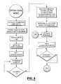
- FIG. 3shows a startup routine for initialization of the ports and determining whether to branch into an operational mode or a test mode.
- FIG. 4shows the logic for the operational mode of the microcontroller 20 .
- FIG. 5shows the logic for a decision making routine following the receipt of an interrupt.
- FIG. 6shows the logic flow when an interrupt occurred and such interrupt was not caused by the sensor circuit.
- FIGS. 7 , and 9show the logic flow to determine whether the up button, down button or function button was pressed and the action needed to be performed.
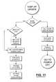
- FIG. 10shows the logic flow for a timer routine for toggling the shutter assembly 14 and the display at a periodic rate.
- FIG. 11shows the logic flow for updating information to the display.
- FIG. 12shows the logic flow of a power off routine.
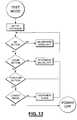
- FIG. 13shows the logic flow for the test mode for calibrating the initial shade values.
- microcontroller 20 utilized to implement the control circuit 12may be affected by non-user activities, such as radiated electromagnetic fields produced during the welding process, such interferences with the operation of the microcontroller 20 can be compensated for within the logic flow of the microcontroller 20 of the eye protection device 10 .
- FIG. 16shown therein is a logic flow for a startup routine for the microcontroller 20 . Determination of whether the startup of the microcontroller 20 was caused by user power-up (e.g. was caused by the on/mode button 90 , or another function key, being pressed), or was not caused by user power-up (e.g.
- occurrences which may trigger a startup which are not a user power-upcan include a reset of a CPU, loss of data, looping in a sub-routine, or loss of timing.
- the logicbranches to a plurality of initialization and calibration routines for the eye protection device 10 . If the startup was not caused by user power-up, then the initialization and calibration routines are bypassed and the logic branches to the main program for the operational mode of the microcontroller 20 , where the main program will run using the stored settings and parameters in use, or previously saved, prior to the startup of the microcontroller 20 .
- the microcontroller 20will not perform the initialization and calibration routines and will instead operate under the same settings and parameters as before the startup caused by the electromagnetic field interruption.
- any customized settings or parameters set by the userwill not be initialized back to default values or have to be reentered by the user, and the shutter assembly 14 will not be initialized and will continue operation from its current state.
- the usersince such an interruption and startup will be essentially instantaneous, the user will typically not detect such an interruption has occurred during use of the eye protection device 10 during the welding process.
- Interference with the operation of the control circuit 12 from electromagnetic fieldscan also be reduced by providing a protective casing for at least a portion of the control circuit 12 .
- a protective casingfor at least a portion of the control circuit 12 .
- the eye protection deviceprovided with a protective casing 304 disposed generally about the control circuit 12 to substantially prevent electromagnetic fields from a weld or from the welding equipment from interfering with the operation of the control circuit 12 .
- the protective casing 304comprises a non-conductive material 312 , wherein the non-conductive material 312 has a first surface 320 and a second surface 324 .
- a conductive material 316is disposed on or in the non-conductive material 312 .
- the conductive material 316may be disposed on the first surface 320 of the non-conductive material 312 , on the second surface 324 of the non-conductive material 312 , between the first surface 320 and the second surface 324 of the non-conductive material 312 , or combinations thereof.
- the non-conductive material 312may be any non-conductive material, or combinations of non-conductive materials, such as for example FR4, plastic, or combinations thereof.
- the conductive material 316is preferably ungrounded and can be any conductive material, or combination of conductive materials, capable of impeding the transmission of electromagnetic fields.
- the conductive material 316can be chrome, nickel, copper, silver, tin, copper tape, conductive paint, or combinations thereof.
- the protective coveringis disposed generally about the control circuit 12 and/or the microcontroller 20 so as to provide a Faraday cage generally about the control circuit 12 and/or the microcontroller 20 .
- the non-conductive material 312can be a non-conductive portion of the housing 102 .
- the non-conductive material 312is the housing 102 and the conductive material 316 is a chrome or nickel plating formed on the first surface 320 of the housing 102 .
- the platingcan be formed from any suitable process, such as electroplating or glueing or molding conductive tape to the housing 102 .
- the protective casing 304comprises copper tape 328 disposed on portions of the second surface of the housing 102 generally adjacent the microcontroller 20 . Further, the protective casing 304 can also include copper tape 328 wrapped around at least one covered wire 414 of the control circuit 12 .
- the conductive material 316 of the protective casing 304includes the copper tape 328
- the non-conductive material 312includes a non-conductive jacket (not shown) of the covered wire 414 of the control circuit 12 .
- the protective casing 304is depicted in FIGS. 17-19 as including the housing 102 as at least a portion of the non-conductive material 312 , it should be understood that the non-conductive material 312 can include non-conductive material that is independent of the housing 102 .
- the non-conductive material 312 of the protective casing 304can be a separate housing disposed generally about at least a portion of the control circuit 12 , including the microcontroller 20 , and/or the user interface circuitry such as the keypad within the housing 102 .
- the non-conductive material 312 of the protective casing 304can be disposed generally about at least a portion of the control circuit 12 , including the microcontroller 20 , outside the housing 102 when at least a portion of the control circuit 12 is disposed outside the housing 102 , such as shown for example in FIG. 21 .
- the conductive material 316could be embedded within the housing 102 or separate from the housing 102 and applied.
Landscapes
- Health & Medical Sciences (AREA)
- Ophthalmology & Optometry (AREA)
- Engineering & Computer Science (AREA)
- Biomedical Technology (AREA)
- Heart & Thoracic Surgery (AREA)
- Vascular Medicine (AREA)
- Life Sciences & Earth Sciences (AREA)
- Animal Behavior & Ethology (AREA)
- General Health & Medical Sciences (AREA)
- Public Health (AREA)
- Veterinary Medicine (AREA)
- Arc Welding Control (AREA)
- Photometry And Measurement Of Optical Pulse Characteristics (AREA)
Abstract
Description
Claims (15)
Priority Applications (1)
| Application Number | Priority Date | Filing Date | Title |
|---|---|---|---|
| US12/138,999US7750283B2 (en) | 2001-05-05 | 2008-06-13 | Microprocessor based automatically dimmable eye protection device with interruption prevention |
Applications Claiming Priority (6)
| Application Number | Priority Date | Filing Date | Title |
|---|---|---|---|
| US28875901P | 2001-05-05 | 2001-05-05 | |
| US10/140,049US6881939B1 (en) | 2001-05-05 | 2002-05-03 | Microprocessor based automatically dimmable eye protection device |
| US10/741,622US6884987B2 (en) | 2001-05-05 | 2003-12-19 | Microprocessor based automatically dimmable eye protection device with interruption prevention |
| US11/089,930US7232988B2 (en) | 2001-05-05 | 2005-05-05 | Microprocessor based automatically dimmable eye protection device with interruption prevention |
| US11/820,059US7755019B1 (en) | 2001-05-05 | 2007-06-18 | Microprocessor based automatically dimmable eye protection device with interruption prevention |
| US12/138,999US7750283B2 (en) | 2001-05-05 | 2008-06-13 | Microprocessor based automatically dimmable eye protection device with interruption prevention |
Related Parent Applications (1)
| Application Number | Title | Priority Date | Filing Date |
|---|---|---|---|
| US11/820,059ContinuationUS7755019B1 (en) | 2001-05-05 | 2007-06-18 | Microprocessor based automatically dimmable eye protection device with interruption prevention |
Publications (2)
| Publication Number | Publication Date |
|---|---|
| US20080308714A1 US20080308714A1 (en) | 2008-12-18 |
| US7750283B2true US7750283B2 (en) | 2010-07-06 |
Family
ID=32965186
Family Applications (6)
| Application Number | Title | Priority Date | Filing Date |
|---|---|---|---|
| US10/140,049Expired - LifetimeUS6881939B1 (en) | 2001-05-05 | 2002-05-03 | Microprocessor based automatically dimmable eye protection device |
| US10/741,622Expired - LifetimeUS6884987B2 (en) | 2001-05-05 | 2003-12-19 | Microprocessor based automatically dimmable eye protection device with interruption prevention |
| US11/089,930Expired - LifetimeUS7232988B2 (en) | 2001-05-05 | 2005-05-05 | Microprocessor based automatically dimmable eye protection device with interruption prevention |
| US11/820,059Expired - Fee RelatedUS7755019B1 (en) | 2001-05-05 | 2007-06-18 | Microprocessor based automatically dimmable eye protection device with interruption prevention |
| US12/138,999Expired - Fee RelatedUS7750283B2 (en) | 2001-05-05 | 2008-06-13 | Microprocessor based automatically dimmable eye protection device with interruption prevention |
| US12/834,594Expired - Fee RelatedUS8119974B2 (en) | 2001-05-05 | 2010-07-12 | Microprocessor based automatically dimmable eye protection device with interruption prevention |
Family Applications Before (4)
| Application Number | Title | Priority Date | Filing Date |
|---|---|---|---|
| US10/140,049Expired - LifetimeUS6881939B1 (en) | 2001-05-05 | 2002-05-03 | Microprocessor based automatically dimmable eye protection device |
| US10/741,622Expired - LifetimeUS6884987B2 (en) | 2001-05-05 | 2003-12-19 | Microprocessor based automatically dimmable eye protection device with interruption prevention |
| US11/089,930Expired - LifetimeUS7232988B2 (en) | 2001-05-05 | 2005-05-05 | Microprocessor based automatically dimmable eye protection device with interruption prevention |
| US11/820,059Expired - Fee RelatedUS7755019B1 (en) | 2001-05-05 | 2007-06-18 | Microprocessor based automatically dimmable eye protection device with interruption prevention |
Family Applications After (1)
| Application Number | Title | Priority Date | Filing Date |
|---|---|---|---|
| US12/834,594Expired - Fee RelatedUS8119974B2 (en) | 2001-05-05 | 2010-07-12 | Microprocessor based automatically dimmable eye protection device with interruption prevention |
Country Status (1)
| Country | Link |
|---|---|
| US (6) | US6881939B1 (en) |
Cited By (1)
| Publication number | Priority date | Publication date | Assignee | Title |
|---|---|---|---|---|
| US20100309156A1 (en)* | 2009-06-03 | 2010-12-09 | Chimei Innolux Corporation | Sensing devices and electronic apparatuses using the same |
Families Citing this family (44)
| Publication number | Priority date | Publication date | Assignee | Title |
|---|---|---|---|---|
| US6881939B1 (en) | 2001-05-05 | 2005-04-19 | Jackson Products, Inc. | Microprocessor based automatically dimmable eye protection device |
| US9495676B2 (en) | 2002-02-05 | 2016-11-15 | Square, Inc. | Method of transmitting information from a power efficient card to a mobile device |
| US9262777B2 (en) | 2002-02-05 | 2016-02-16 | Square, Inc. | Card reader with power efficient architecture that includes a wake-up circuit |
| US9305314B2 (en) | 2002-02-05 | 2016-04-05 | Square, Inc. | Methods of transmitting information to mobile devices using cost effective card readers |
| US9286635B2 (en) | 2002-02-05 | 2016-03-15 | Square, Inc. | Method of transmitting information from efficient communication protocol card readers to mobile devices |
| US9224142B2 (en) | 2002-02-05 | 2015-12-29 | Square, Inc. | Card reader with power efficient architecture that includes a power supply and a wake up circuit |
| WO2005002480A1 (en)* | 2003-07-03 | 2005-01-13 | Lightswitch Safety Systems, Inc. | Multi-stage sensor for an auto-darkening lens for use in welding and method |
| US8181270B2 (en)* | 2005-09-09 | 2012-05-22 | Optrel Ag | Anti-glare protection device |
| KR100737240B1 (en)* | 2005-12-14 | 2007-07-09 | 오토스테크 주식회사 | Control method of glare prevention device for welding light detection |
| US8040309B2 (en)* | 2006-01-31 | 2011-10-18 | Chimei Innolux Corproation | Display panel with image sticking elimination circuit and driving circuit with the same |
| US20080055731A1 (en)* | 2006-08-31 | 2008-03-06 | The Boeing Company | Airplane window control |
| EP2209449B1 (en) | 2007-10-05 | 2014-07-23 | 3M Innovative Properties Company | Automatic darkening filter apparatus and method |
| US20090094721A1 (en)* | 2007-10-11 | 2009-04-16 | Illinois Tool Works Inc. | Automated sensitivity setting for an auto-darkening lens in a welding helmet |
| US20090213283A1 (en)* | 2008-02-27 | 2009-08-27 | Burlingame Robert G | Apparatus and method for adjustable variable transmissivity polarized eye glasses |
| US8115152B1 (en) | 2008-06-03 | 2012-02-14 | ADIC, Inc. | Method of operating a photoconductor in an imaging system, and read-out circuit employing an AC-biased photoconductor |
| US8071935B2 (en)* | 2008-06-30 | 2011-12-06 | Nellcor Puritan Bennett Llc | Optical detector with an overmolded faraday shield |
| KR100943878B1 (en)* | 2008-07-11 | 2010-02-24 | 오토스테크 주식회사 | Digital anti-glare device and control method |
| CN101785725B (en)* | 2010-02-09 | 2013-07-03 | 北京极光安防护科技有限公司 | Auto-darkening welding filter capable of automatically setting shade number |
| US20120256080A9 (en)* | 2010-05-10 | 2012-10-11 | Toyota Motor Engineering & Manufacturing North America, Inc. | Selectively translucent window |
| US8264265B2 (en)* | 2010-09-30 | 2012-09-11 | Kimberly-Clark Worldwide, Inc. | Automatic darkening filter (ADF) eye protection device with improved drive circuitry |
| USD683906S1 (en) | 2010-10-26 | 2013-06-04 | Kimberly-Clark Worldwide, Inc. | Welding auto-darkening filter |
| USD683502S1 (en) | 2010-10-26 | 2013-05-28 | Kimberly-Clark Worldwide, Inc. | Welding auto-darkening filter |
| USD678619S1 (en) | 2010-10-26 | 2013-03-19 | Kimberly-Clark Worldwide, Inc. | Welding auto-darkening filter assembly |
| US9576159B1 (en) | 2011-01-24 | 2017-02-21 | Square, Inc. | Multiple payment card reader system |
| KR101244167B1 (en)* | 2011-03-18 | 2013-03-25 | 주식회사 오토스윙 | Apparatus for preventing from dazzling having self test mode |
| KR20120117121A (en)* | 2011-04-14 | 2012-10-24 | 주식회사 오토스윙 | Apparatus for preventing from dazzling having multi function |
| US10475024B1 (en) | 2012-10-15 | 2019-11-12 | Square, Inc. | Secure smart card transactions |
| US10251786B2 (en) | 2013-11-21 | 2019-04-09 | Optrel Holding AG | Method and apparatus for controlling opening of an auto-darkening filter in an eye protection device |
| US9633236B1 (en) | 2013-12-11 | 2017-04-25 | Square, Inc. | Power harvesting in reader devices |
| CN103713574A (en)* | 2013-12-27 | 2014-04-09 | 上海汇众萨克斯减振器有限公司 | Circuit and control method for automatic four-station bottom cover press fitting and slit bonding special machine |
| US10304043B1 (en) | 2014-05-21 | 2019-05-28 | Square, Inc. | Multi-peripheral host device |
| US9760740B1 (en) | 2014-06-23 | 2017-09-12 | Square, Inc. | Terminal case with integrated dual reader stack |
| US10285864B2 (en) | 2014-07-25 | 2019-05-14 | Snap-On Incorporated | Auto-darkening welding helmet |
| US9799025B2 (en) | 2014-08-19 | 2017-10-24 | Square, Inc. | Energy harvesting bidirectional audio interface |
| US9922460B2 (en) | 2014-11-04 | 2018-03-20 | Illinois Tool Works Inc. | Stereoscopic helmet display |
| US10032388B2 (en) | 2014-12-05 | 2018-07-24 | Illinois Tool Works Inc. | Augmented and mediated reality welding helmet systems |
| US10753982B2 (en) | 2014-12-09 | 2020-08-25 | Square, Inc. | Monitoring battery health of a battery used in a device |
| US9355285B1 (en)* | 2015-02-12 | 2016-05-31 | Square, Inc. | Tone-based wake up circuit for card reader |
| USD816746S1 (en)* | 2015-12-03 | 2018-05-01 | Antra Technologies Co., Ltd. | Auto-darkening welding filter |
| CN108904130B (en)* | 2018-07-13 | 2023-12-19 | 上海东软载波微电子有限公司 | Electric welding mirror |
| US20200114456A1 (en)* | 2018-10-10 | 2020-04-16 | Lincoln Global, Inc. | Systems and methods including a head-mounted device for use in arc welding |
| EP3749266B1 (en) | 2018-10-23 | 2023-06-07 | Tecmen Electronics Co., Ltd | Auto-darkening welding helmet |
| FR3117905B1 (en)* | 2020-12-17 | 2023-04-21 | Gys | TIG-type tacking process for two sheets or parts, corresponding welding process and welding station |
| US20240285440A1 (en) | 2021-09-21 | 2024-08-29 | 3M Innovative Properties Company | Welding protection device with haptic sensing |
Citations (70)
| Publication number | Priority date | Publication date | Assignee | Title |
|---|---|---|---|---|
| GB325586A (en) | 1928-11-22 | 1930-02-24 | British Thomson Houston Co Ltd | Improvements relating to devices for protecting a person from the radiations of an electric arc |
| US2423320A (en) | 1944-07-29 | 1947-07-01 | Jr Samuel C Hurley | Welder's helmet |
| US2548230A (en) | 1946-06-27 | 1951-04-10 | Molyneux & Aspinwall Inc | Welding mask |
| US2761046A (en) | 1953-02-16 | 1956-08-28 | Herrick James Elder | Automatic arc welding viewing mechanism |
| US3137784A (en) | 1961-02-27 | 1964-06-16 | Kasemann Erwin | Device for protecting the eyes of welders |
| US3159844A (en) | 1962-11-09 | 1964-12-08 | Samuel C Halpert | Electromagnetically controlled hood device for welding and cutting |
| US3245315A (en) | 1962-09-05 | 1966-04-12 | Alvin M Marks | Electro-optic responsive flashblindness controlling device |
| US3575491A (en) | 1968-10-16 | 1971-04-20 | Rca Corp | Decreasing response time of liquid crystals |
| US3731986A (en) | 1971-04-22 | 1973-05-08 | Int Liquid Xtal Co | Display devices utilizing liquid crystal light modulation |
| DE2315308A1 (en) | 1972-03-27 | 1973-10-11 | Aga Ab | DEVICE FOR PROTECTING THE HUMAN EYE AGAINST RADIATION |
| US3873804A (en) | 1972-04-14 | 1975-03-25 | Mack Gordon | Welding helmet with eye piece control |
| US3881808A (en) | 1973-12-07 | 1975-05-06 | Motorola Inc | Liquid crystal light control device having a high transmission efficiency |
| US3881809A (en) | 1972-03-10 | 1975-05-06 | Hoffmann La Roche | Reflection system for liquid crystal displays |
| US3890628A (en) | 1973-10-23 | 1975-06-17 | Motorola Inc | Liquid crystal light control device and circuit |
| US3918796A (en) | 1971-02-09 | 1975-11-11 | Hoffmann La Roche | Liquid-crystal non-linear light modulators using electric and magnetic fields |
| US3967881A (en) | 1974-04-04 | 1976-07-06 | Matsushita Electric Industrial Co., Ltd. | Liquid crystal display |
| SE394755B (en) | 1972-09-19 | 1977-07-04 | Sharp Kk | LIQUID CRYSTAL INDICATOR |
| US4039803A (en) | 1976-04-08 | 1977-08-02 | Mack Gordon | Electro-optic welding helmet lens assembly |
| SE7608690L (en) | 1975-03-07 | 1978-02-04 | Hornell Ake | OPTICAL FILTER |
| US4071912A (en) | 1974-12-02 | 1978-02-07 | Revue Thommen Ag | Light filter for welder's mask |
| USRE29684E (en) | 1973-12-26 | 1978-06-27 | Welding helmet with eye piece control | |
| US4155122A (en) | 1975-12-02 | 1979-05-22 | Revue Thommen Ag | Light shield for welder's mask |
| JPS5592276A (en) | 1978-12-28 | 1980-07-12 | Susumu Nishikawa | Protector for arc welding |
| US4237557A (en) | 1979-07-30 | 1980-12-09 | Mack Gordon | Control system for welding helmet liquid crystal light shutter |
| US4240709A (en) | 1978-04-24 | 1980-12-23 | Esab Aktiebolag | Multiple layer protective glass, particularly a protective glass for a welding shield |
| US4279474A (en) | 1980-03-25 | 1981-07-21 | Belgorod Barry M | Spectacle lens having continuously variable controlled density and fast response time |
| US4328490A (en) | 1979-06-29 | 1982-05-04 | Tokyo Shibaura Denki Kabushiki Kaisha | Liquid crystal display device with low battery indication |
| US4385806A (en) | 1978-06-08 | 1983-05-31 | Fergason James L | Liquid crystal display with improved angle of view and response times |
| FR2530039A1 (en) | 1982-07-06 | 1984-01-13 | Cuvelier Antoine | Safety (protective) glasses having automatically adjustable transmission using liquid crystals |
| US4435047A (en) | 1981-09-16 | 1984-03-06 | Manchester R & D Partnership | Encapsulated liquid crystal and method |
| US4436376A (en) | 1980-02-13 | 1984-03-13 | Fergason James L | Light modulator, demodulator and method of communication employing the same |
| JPS59111102A (en) | 1982-12-16 | 1984-06-27 | Nippon Denso Co Ltd | Glare shielding type reflecting mirror |
| US4540243A (en) | 1981-02-17 | 1985-09-10 | Fergason James L | Method and apparatus for converting phase-modulated light to amplitude-modulated light and communication method and apparatus employing the same |
| EP0157744A1 (en) | 1984-02-24 | 1985-10-09 | Peter Toth | Optical filter for protective welding lens assemblies |
| US4556289A (en) | 1983-03-21 | 1985-12-03 | Manchester R & D Partnership | Low birefringence encapsulated liquid crystal and optical shutter using same |
| US4560239A (en) | 1984-02-29 | 1985-12-24 | Amnon Katz | Liquid crystal active light shield |
| US4582396A (en) | 1983-05-09 | 1986-04-15 | Tektronix, Inc. | Field sequential color display system using optical retardation |
| USRE32521E (en) | 1978-06-08 | 1987-10-13 | Fergason James L | Light demodulator and method of communication employing the same |
| US4710694A (en) | 1986-06-02 | 1987-12-01 | Acme Electric Corporation | Microprocessor controlled battery charger |
| US4759608A (en) | 1985-12-31 | 1988-07-26 | Yang Jong P | Automatic liquid crystal light-shutter |
| US4813766A (en) | 1988-03-02 | 1989-03-21 | Raytheon Company | Optical time delay apparatus |
| US4821292A (en) | 1987-06-03 | 1989-04-11 | General Electric Company | Adaptive limiter/detector which changes time constant upon detection of dotting pattern |
| US4863244A (en) | 1988-03-11 | 1989-09-05 | Optrel Ag | Electro-optic welding lens assembly |
| EP0335056A1 (en) | 1986-10-09 | 1989-10-04 | Optrel Ag | Light filter with automatic optical transmission control |
| US4877310A (en) | 1988-08-04 | 1989-10-31 | Xerox Corporation | Electronically variable MTF filter for image sensor arrays |
| EP0349665A1 (en) | 1988-07-07 | 1990-01-10 | Optrel Ag | An electro-optic welding lens assembly |
| US4901074A (en) | 1987-12-31 | 1990-02-13 | Whirlpool Corporation | Glass membrane keyboard switch assembly for domestic appliance |
| US4928181A (en) | 1988-11-21 | 1990-05-22 | Philip Morris Incorporated | Methods and apparatus for optically enhancing selected features in an input image |
| WO1990014809A1 (en) | 1989-06-05 | 1990-12-13 | Hörnell Elektrooptik Ab | A welder's helmet |
| US5015086A (en) | 1989-04-17 | 1991-05-14 | Seiko Epson Corporation | Electronic sunglasses |
| US5074647A (en) | 1989-12-07 | 1991-12-24 | Optical Shields, Inc. | Liquid crystal lens assembly for eye protection |
| US5113270A (en) | 1988-10-19 | 1992-05-12 | Fergason James L | Variable density light control apparatus |
| US5184156A (en) | 1991-11-12 | 1993-02-02 | Reliant Laser Corporation | Glasses with color-switchable, multi-layered lenses |
| US5208688A (en) | 1991-02-08 | 1993-05-04 | Osd Envizion Company | Eye protection device for welding helmets |
| US5248880A (en) | 1991-03-25 | 1993-09-28 | Osd Envizion Company | Detector system for detecting the occurrence of welding |
| US5252817A (en) | 1991-03-25 | 1993-10-12 | Osd Envizion Company | Detector system for detecting the occurrence of welding using detector feedback |
| US5347383A (en) | 1989-06-12 | 1994-09-13 | Osd Envizion Company | High speed, low power driving circuit for liquid crystal shutter |
| US5377032A (en) | 1993-02-05 | 1994-12-27 | Osd Envizion Company | Electro-optic light shutter and frame assembly with integrated switching mechanism |
| US5420502A (en) | 1992-12-21 | 1995-05-30 | Schweitzer, Jr.; Edmund O. | Fault indicator with optically-isolated remote readout circuit |
| US5519522A (en) | 1993-08-11 | 1996-05-21 | Fergason; Jeffrey K. | Eye protection device for welding helmets and the like with hot mirror and indium tin oxide layer |
| US5671035A (en) | 1995-06-07 | 1997-09-23 | Barnes; Elwood E. | Light intensity reduction apparatus and method |
| US5751258A (en) | 1991-03-25 | 1998-05-12 | Osd Envizion, Inc. | Liquid crystal lens driver electronics for eye protection, high speed shuttering with consistent performance |
| US6067129A (en) | 1996-03-15 | 2000-05-23 | Osd Envizion, Inc. | Welding lens with integrated display and method |
| US6070264A (en) | 1999-04-09 | 2000-06-06 | Jackson Products, Inc. | Welding helmet having auto-darkening and manually adjustable lens shade control |
| US6483090B1 (en) | 1998-12-29 | 2002-11-19 | Otos Co., Ltd. | Glare protecting device and method of controlling thereof |
| US6552316B1 (en) | 1998-12-29 | 2003-04-22 | Otos Co., Ltd. | Glare protecting device utilizing both optical and non-optical detectors and method of controlling thereof |
| US6614409B1 (en) | 1999-11-23 | 2003-09-02 | Otos Co., Ltd. | Glare shielding device of welding helmet and method of controlling the same |
| US6796652B1 (en) | 1999-09-29 | 2004-09-28 | Optrel Ag | Glare-protection device with a screened evaluation circuit |
| US6815652B1 (en) | 2000-09-11 | 2004-11-09 | Jackson Products, Inc. | Low power phototransistor-based welding helmet providing reduced sensitivity to low intensity light and sharp phototransistor response to high intensity light |
| US6841772B1 (en) | 2001-05-05 | 2005-01-11 | Jackson Products, Inc. | Eye-protection device having dual high voltage switching |
Family Cites Families (11)
| Publication number | Priority date | Publication date | Assignee | Title |
|---|---|---|---|---|
| US29684A (en)* | 1860-08-21 | Coupling for belts | ||
| US2761048A (en) | 1953-06-25 | 1956-08-28 | Ohio Crankshaft Co | High-frequency inductor |
| US3697881A (en)* | 1969-07-10 | 1972-10-10 | Kokusai Denshin Denwa Co Ltd | Phase detection system for at least one digital phase-modulated wave |
| JPS4910017A (en)* | 1972-05-24 | 1974-01-29 | ||
| US3873801A (en)* | 1973-06-15 | 1975-03-25 | Iv Thomas B Hutchins | Assembly of electrical-deflection-sensitive transducer |
| JPS5992276A (en) | 1982-11-17 | 1984-05-28 | 川崎重工業株式会社 | Motorcycle cowling mounting structure |
| JPH0738309B2 (en)* | 1986-09-30 | 1995-04-26 | ヒロセ電機株式会社 | Electric connector and its connection method |
| DE4445125A1 (en)* | 1994-12-17 | 1996-06-20 | Wabco Gmbh | Housing for an electrical component |
| US6444942B1 (en)* | 1999-08-03 | 2002-09-03 | Nadex Co. Ltd | Welding control systems |
| US6881939B1 (en) | 2001-05-05 | 2005-04-19 | Jackson Products, Inc. | Microprocessor based automatically dimmable eye protection device |
| WO2005017636A2 (en)* | 2003-08-11 | 2005-02-24 | Hamilton Thomas J | Eye-protection device having dual high voltage switching |
- 2002
- 2002-05-03USUS10/140,049patent/US6881939B1/ennot_activeExpired - Lifetime
- 2003
- 2003-12-19USUS10/741,622patent/US6884987B2/ennot_activeExpired - Lifetime
- 2005
- 2005-05-05USUS11/089,930patent/US7232988B2/ennot_activeExpired - Lifetime
- 2007
- 2007-06-18USUS11/820,059patent/US7755019B1/ennot_activeExpired - Fee Related
- 2008
- 2008-06-13USUS12/138,999patent/US7750283B2/ennot_activeExpired - Fee Related
- 2010
- 2010-07-12USUS12/834,594patent/US8119974B2/ennot_activeExpired - Fee Related
Patent Citations (75)
| Publication number | Priority date | Publication date | Assignee | Title |
|---|---|---|---|---|
| GB325586A (en) | 1928-11-22 | 1930-02-24 | British Thomson Houston Co Ltd | Improvements relating to devices for protecting a person from the radiations of an electric arc |
| US2423320A (en) | 1944-07-29 | 1947-07-01 | Jr Samuel C Hurley | Welder's helmet |
| US2548230A (en) | 1946-06-27 | 1951-04-10 | Molyneux & Aspinwall Inc | Welding mask |
| US2761046A (en) | 1953-02-16 | 1956-08-28 | Herrick James Elder | Automatic arc welding viewing mechanism |
| US3137784A (en) | 1961-02-27 | 1964-06-16 | Kasemann Erwin | Device for protecting the eyes of welders |
| US3245315A (en) | 1962-09-05 | 1966-04-12 | Alvin M Marks | Electro-optic responsive flashblindness controlling device |
| US3159844A (en) | 1962-11-09 | 1964-12-08 | Samuel C Halpert | Electromagnetically controlled hood device for welding and cutting |
| US3575491A (en) | 1968-10-16 | 1971-04-20 | Rca Corp | Decreasing response time of liquid crystals |
| US3918796A (en) | 1971-02-09 | 1975-11-11 | Hoffmann La Roche | Liquid-crystal non-linear light modulators using electric and magnetic fields |
| US3731986A (en) | 1971-04-22 | 1973-05-08 | Int Liquid Xtal Co | Display devices utilizing liquid crystal light modulation |
| US3881809A (en) | 1972-03-10 | 1975-05-06 | Hoffmann La Roche | Reflection system for liquid crystal displays |
| DE2315308A1 (en) | 1972-03-27 | 1973-10-11 | Aga Ab | DEVICE FOR PROTECTING THE HUMAN EYE AGAINST RADIATION |
| US3873804A (en) | 1972-04-14 | 1975-03-25 | Mack Gordon | Welding helmet with eye piece control |
| SE394755B (en) | 1972-09-19 | 1977-07-04 | Sharp Kk | LIQUID CRYSTAL INDICATOR |
| US3890628A (en) | 1973-10-23 | 1975-06-17 | Motorola Inc | Liquid crystal light control device and circuit |
| US3881808A (en) | 1973-12-07 | 1975-05-06 | Motorola Inc | Liquid crystal light control device having a high transmission efficiency |
| USRE29684E (en) | 1973-12-26 | 1978-06-27 | Welding helmet with eye piece control | |
| US3967881A (en) | 1974-04-04 | 1976-07-06 | Matsushita Electric Industrial Co., Ltd. | Liquid crystal display |
| US4071912A (en) | 1974-12-02 | 1978-02-07 | Revue Thommen Ag | Light filter for welder's mask |
| SE7608690L (en) | 1975-03-07 | 1978-02-04 | Hornell Ake | OPTICAL FILTER |
| US4155122A (en) | 1975-12-02 | 1979-05-22 | Revue Thommen Ag | Light shield for welder's mask |
| US4039803A (en) | 1976-04-08 | 1977-08-02 | Mack Gordon | Electro-optic welding helmet lens assembly |
| US4240709A (en) | 1978-04-24 | 1980-12-23 | Esab Aktiebolag | Multiple layer protective glass, particularly a protective glass for a welding shield |
| USRE32521E (en) | 1978-06-08 | 1987-10-13 | Fergason James L | Light demodulator and method of communication employing the same |
| US4385806A (en) | 1978-06-08 | 1983-05-31 | Fergason James L | Liquid crystal display with improved angle of view and response times |
| USRE32521F1 (en) | 1978-06-08 | 1990-09-18 | James L Fergason | Light modulator demodulator and method of communication employing the same |
| JPS5592276A (en) | 1978-12-28 | 1980-07-12 | Susumu Nishikawa | Protector for arc welding |
| US4328490A (en) | 1979-06-29 | 1982-05-04 | Tokyo Shibaura Denki Kabushiki Kaisha | Liquid crystal display device with low battery indication |
| US4237557A (en) | 1979-07-30 | 1980-12-09 | Mack Gordon | Control system for welding helmet liquid crystal light shutter |
| US4436376A (en) | 1980-02-13 | 1984-03-13 | Fergason James L | Light modulator, demodulator and method of communication employing the same |
| US4279474A (en) | 1980-03-25 | 1981-07-21 | Belgorod Barry M | Spectacle lens having continuously variable controlled density and fast response time |
| US4540243A (en) | 1981-02-17 | 1985-09-10 | Fergason James L | Method and apparatus for converting phase-modulated light to amplitude-modulated light and communication method and apparatus employing the same |
| US4540243B1 (en) | 1981-02-17 | 1990-09-18 | James L Fergason | |
| US4435047A (en) | 1981-09-16 | 1984-03-06 | Manchester R & D Partnership | Encapsulated liquid crystal and method |
| FR2530039A1 (en) | 1982-07-06 | 1984-01-13 | Cuvelier Antoine | Safety (protective) glasses having automatically adjustable transmission using liquid crystals |
| JPS59111102A (en) | 1982-12-16 | 1984-06-27 | Nippon Denso Co Ltd | Glare shielding type reflecting mirror |
| US4664479A (en) | 1982-12-16 | 1987-05-12 | Nippondenso Co., Ltd. | Dynamic scattering, guest host, non-glaring reflector |
| US4556289A (en) | 1983-03-21 | 1985-12-03 | Manchester R & D Partnership | Low birefringence encapsulated liquid crystal and optical shutter using same |
| US4582396A (en) | 1983-05-09 | 1986-04-15 | Tektronix, Inc. | Field sequential color display system using optical retardation |
| US4728173A (en) | 1984-02-24 | 1988-03-01 | Peter Toth | Optical filter for protective welding lens assemblies |
| EP0157744A1 (en) | 1984-02-24 | 1985-10-09 | Peter Toth | Optical filter for protective welding lens assemblies |
| US4560239A (en) | 1984-02-29 | 1985-12-24 | Amnon Katz | Liquid crystal active light shield |
| US4759608A (en) | 1985-12-31 | 1988-07-26 | Yang Jong P | Automatic liquid crystal light-shutter |
| US4710694A (en) | 1986-06-02 | 1987-12-01 | Acme Electric Corporation | Microprocessor controlled battery charger |
| EP0335056A1 (en) | 1986-10-09 | 1989-10-04 | Optrel Ag | Light filter with automatic optical transmission control |
| US4821292A (en) | 1987-06-03 | 1989-04-11 | General Electric Company | Adaptive limiter/detector which changes time constant upon detection of dotting pattern |
| US4901074A (en) | 1987-12-31 | 1990-02-13 | Whirlpool Corporation | Glass membrane keyboard switch assembly for domestic appliance |
| US4813766A (en) | 1988-03-02 | 1989-03-21 | Raytheon Company | Optical time delay apparatus |
| US4863244A (en) | 1988-03-11 | 1989-09-05 | Optrel Ag | Electro-optic welding lens assembly |
| EP0349665A1 (en) | 1988-07-07 | 1990-01-10 | Optrel Ag | An electro-optic welding lens assembly |
| US4877310A (en) | 1988-08-04 | 1989-10-31 | Xerox Corporation | Electronically variable MTF filter for image sensor arrays |
| US5113270A (en) | 1988-10-19 | 1992-05-12 | Fergason James L | Variable density light control apparatus |
| US4928181A (en) | 1988-11-21 | 1990-05-22 | Philip Morris Incorporated | Methods and apparatus for optically enhancing selected features in an input image |
| US5015086A (en) | 1989-04-17 | 1991-05-14 | Seiko Epson Corporation | Electronic sunglasses |
| WO1990014809A1 (en) | 1989-06-05 | 1990-12-13 | Hörnell Elektrooptik Ab | A welder's helmet |
| US5347383A (en) | 1989-06-12 | 1994-09-13 | Osd Envizion Company | High speed, low power driving circuit for liquid crystal shutter |
| US5074647A (en) | 1989-12-07 | 1991-12-24 | Optical Shields, Inc. | Liquid crystal lens assembly for eye protection |
| US5208688A (en) | 1991-02-08 | 1993-05-04 | Osd Envizion Company | Eye protection device for welding helmets |
| US5248880A (en) | 1991-03-25 | 1993-09-28 | Osd Envizion Company | Detector system for detecting the occurrence of welding |
| US5252817A (en) | 1991-03-25 | 1993-10-12 | Osd Envizion Company | Detector system for detecting the occurrence of welding using detector feedback |
| US5751258A (en) | 1991-03-25 | 1998-05-12 | Osd Envizion, Inc. | Liquid crystal lens driver electronics for eye protection, high speed shuttering with consistent performance |
| US5184156A (en) | 1991-11-12 | 1993-02-02 | Reliant Laser Corporation | Glasses with color-switchable, multi-layered lenses |
| US5420502A (en) | 1992-12-21 | 1995-05-30 | Schweitzer, Jr.; Edmund O. | Fault indicator with optically-isolated remote readout circuit |
| US5377032A (en) | 1993-02-05 | 1994-12-27 | Osd Envizion Company | Electro-optic light shutter and frame assembly with integrated switching mechanism |
| US5519522A (en) | 1993-08-11 | 1996-05-21 | Fergason; Jeffrey K. | Eye protection device for welding helmets and the like with hot mirror and indium tin oxide layer |
| US5671035A (en) | 1995-06-07 | 1997-09-23 | Barnes; Elwood E. | Light intensity reduction apparatus and method |
| US6067129A (en) | 1996-03-15 | 2000-05-23 | Osd Envizion, Inc. | Welding lens with integrated display and method |
| US6483090B1 (en) | 1998-12-29 | 2002-11-19 | Otos Co., Ltd. | Glare protecting device and method of controlling thereof |
| US6552316B1 (en) | 1998-12-29 | 2003-04-22 | Otos Co., Ltd. | Glare protecting device utilizing both optical and non-optical detectors and method of controlling thereof |
| US6070264A (en) | 1999-04-09 | 2000-06-06 | Jackson Products, Inc. | Welding helmet having auto-darkening and manually adjustable lens shade control |
| US6796652B1 (en) | 1999-09-29 | 2004-09-28 | Optrel Ag | Glare-protection device with a screened evaluation circuit |
| US6614409B1 (en) | 1999-11-23 | 2003-09-02 | Otos Co., Ltd. | Glare shielding device of welding helmet and method of controlling the same |
| US6815652B1 (en) | 2000-09-11 | 2004-11-09 | Jackson Products, Inc. | Low power phototransistor-based welding helmet providing reduced sensitivity to low intensity light and sharp phototransistor response to high intensity light |
| US6841772B1 (en) | 2001-05-05 | 2005-01-11 | Jackson Products, Inc. | Eye-protection device having dual high voltage switching |
| US20070145234A1 (en)* | 2001-05-05 | 2007-06-28 | Hamilton Thomas J | Eye-protection device having dual high voltage switching |
Cited By (2)
| Publication number | Priority date | Publication date | Assignee | Title |
|---|---|---|---|---|
| US20100309156A1 (en)* | 2009-06-03 | 2010-12-09 | Chimei Innolux Corporation | Sensing devices and electronic apparatuses using the same |
| US8575535B2 (en)* | 2009-06-03 | 2013-11-05 | Chimei Innolux Corporation | Sensing devices and electronic apparatuses using the same |
Also Published As
| Publication number | Publication date |
|---|---|
| US20080308714A1 (en) | 2008-12-18 |
| US7232988B2 (en) | 2007-06-19 |
| US6884987B2 (en) | 2005-04-26 |
| US7755019B1 (en) | 2010-07-13 |
| US20110122473A1 (en) | 2011-05-26 |
| US20050253057A1 (en) | 2005-11-17 |
| US20040178326A1 (en) | 2004-09-16 |
| US8119974B2 (en) | 2012-02-21 |
| US6881939B1 (en) | 2005-04-19 |
Similar Documents
| Publication | Publication Date | Title |
|---|---|---|
| US7750283B2 (en) | Microprocessor based automatically dimmable eye protection device with interruption prevention | |
| US4863244A (en) | Electro-optic welding lens assembly | |
| US7659495B2 (en) | Auto darkening eye protection device having a regulated solar power supply | |
| US5248880A (en) | Detector system for detecting the occurrence of welding | |
| US6070264A (en) | Welding helmet having auto-darkening and manually adjustable lens shade control | |
| US7868278B2 (en) | Eye-protection device having dual high voltage switching | |
| US8955162B2 (en) | Welding helmet including anti-blinding device to selectively and conveniently control welding operation and grinding operation | |
| US6614409B1 (en) | Glare shielding device of welding helmet and method of controlling the same | |
| US20090094721A1 (en) | Automated sensitivity setting for an auto-darkening lens in a welding helmet | |
| US4620322A (en) | Electro-optic welding lens assembly | |
| US8049151B2 (en) | Digital type anti-glare device using touch and method of controlling the same | |
| USRE45677E1 (en) | Anti-glare protection device | |
| EP0349665A1 (en) | An electro-optic welding lens assembly | |
| US7462806B2 (en) | Dazzle prevention device having electro magnetic wave detection function and detection mode selection | |
| US6815652B1 (en) | Low power phototransistor-based welding helmet providing reduced sensitivity to low intensity light and sharp phototransistor response to high intensity light | |
| KR100611935B1 (en) | Device for preventing from dazzling with detecting microwave | |
| JPH1174957A (en) | LED control circuit and control method for light-emitting button type telephone | |
| KR100480062B1 (en) | Backlight control method for mobile communication device |
Legal Events
| Date | Code | Title | Description |
|---|---|---|---|
| AS | Assignment | Owner name:KIMBERLY-CLARK CORPORATION,TEXAS Free format text:MERGER;ASSIGNOR:JACKSON PRODUCTS, INC.;REEL/FRAME:023905/0370 Effective date:20091231 Owner name:KIMBERLY-CLARK CORPORATION, TEXAS Free format text:MERGER;ASSIGNOR:JACKSON PRODUCTS, INC.;REEL/FRAME:023905/0370 Effective date:20091231 | |
| AS | Assignment | Owner name:KIMBERLY-CLARK WORLDWIDE, INC.,WISCONSIN Free format text:DECREE OF DISTRIBUTION;ASSIGNOR:KIMBERLY-CLARK CORPORATION;REEL/FRAME:023963/0123 Effective date:20091231 Owner name:KIMBERLY-CLARK WORLDWIDE, INC., WISCONSIN Free format text:DECREE OF DISTRIBUTION;ASSIGNOR:KIMBERLY-CLARK CORPORATION;REEL/FRAME:023963/0123 Effective date:20091231 | |
| STCF | Information on status: patent grant | Free format text:PATENTED CASE | |
| FPAY | Fee payment | Year of fee payment:4 | |
| AS | Assignment | Owner name:KIMBERLY-CLARK WORLDWIDE, INC., WISCONSIN Free format text:NAME CHANGE;ASSIGNOR:KIMBERLY-CLARK WORLDWIDE, INC.;REEL/FRAME:034880/0704 Effective date:20150101 | |
| MAFP | Maintenance fee payment | Free format text:PAYMENT OF MAINTENANCE FEE, 8TH YEAR, LARGE ENTITY (ORIGINAL EVENT CODE: M1552) Year of fee payment:8 | |
| FEPP | Fee payment procedure | Free format text:MAINTENANCE FEE REMINDER MAILED (ORIGINAL EVENT CODE: REM.); ENTITY STATUS OF PATENT OWNER: LARGE ENTITY | |
| LAPS | Lapse for failure to pay maintenance fees | Free format text:PATENT EXPIRED FOR FAILURE TO PAY MAINTENANCE FEES (ORIGINAL EVENT CODE: EXP.); ENTITY STATUS OF PATENT OWNER: LARGE ENTITY | |
| STCH | Information on status: patent discontinuation | Free format text:PATENT EXPIRED DUE TO NONPAYMENT OF MAINTENANCE FEES UNDER 37 CFR 1.362 | |
| FP | Lapsed due to failure to pay maintenance fee | Effective date:20220706 |