US7748912B2 - Double mold optocouplers - Google Patents
Double mold optocouplersDownload PDFInfo
- Publication number
- US7748912B2 US7748912B2US11/205,730US20573005AUS7748912B2US 7748912 B2US7748912 B2US 7748912B2US 20573005 AUS20573005 AUS 20573005AUS 7748912 B2US7748912 B2US 7748912B2
- Authority
- US
- United States
- Prior art keywords
- light
- emitter
- encapsulate
- photodetector
- lens
- Prior art date
- Legal status (The legal status is an assumption and is not a legal conclusion. Google has not performed a legal analysis and makes no representation as to the accuracy of the status listed.)
- Expired - Fee Related, expires
Links
Images


Classifications
- H—ELECTRICITY
- H10—SEMICONDUCTOR DEVICES; ELECTRIC SOLID-STATE DEVICES NOT OTHERWISE PROVIDED FOR
- H10F—INORGANIC SEMICONDUCTOR DEVICES SENSITIVE TO INFRARED RADIATION, LIGHT, ELECTROMAGNETIC RADIATION OF SHORTER WAVELENGTH OR CORPUSCULAR RADIATION
- H10F55/00—Radiation-sensitive semiconductor devices covered by groups H10F10/00, H10F19/00 or H10F30/00 being structurally associated with electric light sources and electrically or optically coupled thereto
- H10F55/18—Radiation-sensitive semiconductor devices covered by groups H10F10/00, H10F19/00 or H10F30/00 being structurally associated with electric light sources and electrically or optically coupled thereto wherein the radiation-sensitive semiconductor devices and the electric light source share a common body having dual-functionality of light emission and light detection
- G—PHYSICS
- G02—OPTICS
- G02B—OPTICAL ELEMENTS, SYSTEMS OR APPARATUS
- G02B6/00—Light guides; Structural details of arrangements comprising light guides and other optical elements, e.g. couplings
- G02B6/24—Coupling light guides
- G02B6/42—Coupling light guides with opto-electronic elements
- G02B6/4201—Packages, e.g. shape, construction, internal or external details
- G02B6/4204—Packages, e.g. shape, construction, internal or external details the coupling comprising intermediate optical elements, e.g. lenses, holograms
- G—PHYSICS
- G02—OPTICS
- G02B—OPTICAL ELEMENTS, SYSTEMS OR APPARATUS
- G02B6/00—Light guides; Structural details of arrangements comprising light guides and other optical elements, e.g. couplings
- G02B6/24—Coupling light guides
- G02B6/42—Coupling light guides with opto-electronic elements
- G02B6/4201—Packages, e.g. shape, construction, internal or external details
- G02B6/4246—Bidirectionally operating package structures
- G—PHYSICS
- G02—OPTICS
- G02B—OPTICAL ELEMENTS, SYSTEMS OR APPARATUS
- G02B6/00—Light guides; Structural details of arrangements comprising light guides and other optical elements, e.g. couplings
- G02B6/24—Coupling light guides
- G02B6/42—Coupling light guides with opto-electronic elements
- G02B6/4201—Packages, e.g. shape, construction, internal or external details
- G02B6/4251—Sealed packages
- G02B6/4253—Sealed packages by embedding housing components in an adhesive or a polymer material
- G—PHYSICS
- G02—OPTICS
- G02B—OPTICAL ELEMENTS, SYSTEMS OR APPARATUS
- G02B6/00—Light guides; Structural details of arrangements comprising light guides and other optical elements, e.g. couplings
- G02B6/24—Coupling light guides
- G02B6/42—Coupling light guides with opto-electronic elements
- G02B6/4201—Packages, e.g. shape, construction, internal or external details
- G02B6/4274—Electrical aspects
- G02B6/428—Electrical aspects containing printed circuit boards [PCB]
Definitions
- the present inventionis generally related to optoelectronic devices and specifically to double mold optocouplers.
- Optocouplersare often used to provide galvanic isolation between different voltage sources in an electronic circuit. Functions of optocouplers include providing high voltage package isolation and isolating noise of a main signal from a resulting signal. In an electronic circuit, an optocoupler ensures electric isolation.
- optocouplersare used in applications such as telecommunications equipment, programmable controllers, direct current (DC) to DC converters, switch-mode power supplies, alternating current (AC) to DC converters and battery chargers.
- Optocouplersare disclosed and discussed in Vishay Telefunken, “General Description Basic Function”; Vishay “Optoelectronics”; Mikami et al., U.S. Pat. No. 4,614,958; Brown, U.S. Pat. No. 5,150,438; and Gempe et al., U.S. Pat. No. 6,013,251, the disclosures of each of which are hereby incorporated herein by reference.
- An optocouplermay be considered comparable to a transformer or relay in some cases. However, optocouplers are typically smaller, ensure considerably shorter switching times, eliminate contact bounce, eliminate interference caused by arcs, and do not experience mechanical wear. Thus, optocouplers are particularly well suited for circuits used in microelectronics and also in data processing and telecommunication systems. Optocouplers are also used to promote component safety, such as in switch-mode power supplies.
- a control circuit or the likeis typically located on one side of the optocoupler, for example the emitter side, while a load circuit is located on the other side, the detector side in this example.
- the circuitsare electrically isolated from each other by the optocoupler. Signals from the control circuit are transmitted optically to the load circuit, and are therefore free of reciprocal effects.
- optical transmission by an optocoupleremploys light beams with wavelengths spanning from the red to infrared range.
- the bandwidth of signals transmitted by an optocouplertypically range from a DC voltage signal to frequencies in the MHz band, although signal frequencies in the GHz range are possible.
- FIG. 1shows an optocoupler configuration representative of the majority of optocoupler packages found today.
- optocoupler package 100defines light emitting device or diode (LED) 102 directly above detector 104 separated by generally transparent insulating material 109 .
- lead 103coupled to LED 102 and lead 106 coupled to detector 104 by bond wire 105 .
- Leads 103 and 106provide signal communication between components of optocoupler package 100 and those external thereto.
- the package heightis limited by at least the sum of the device heights (height of LED 102 plus the height of detector 104 ), with additional material such as transparent insulating material 109 and mold compound 107 required to complete the package adding to the package height.
- additional materialsuch as transparent insulating material 109 and mold compound 107 required to complete the package adding to the package height.
- FIG. 2shows an optocoupler package configuration representative of those described in U.S. Pat. Nos. 5,150,438 and 6,031,251, referenced above.
- FIG. 2shows an in-line or coplanar arrangement for a wide body optocoupler package 200 , providing a reduced optocoupler profile or height (although this configuration may have a larger substrate footprint than optocoupler package 100 ).
- Such coplanar optocoupler packagestypically employs a transparent insulation material 209 , such as silicone, surrounding LED 202 and detector 204 .
- a reflective material 211such as a white coating may coat transparent material 209 .
- Mold compound 207encapsulates the components of optocoupler package 200 . Also shown in FIG.
- Leads 203 and 206provide signal communication between components of optocoupler package 200 and those external thereto, such as devices disposed upon printed circuit board 201 .
- Typical processes of creating both the clear insulation 209 and reflective layer 211are cumbersome, slow and expensive, as the entire clear silicone insulate must be enclosed to restrict the LED light from escaping into mold compound 207 .
- the shape of the optocoupler's profile, especially the clear silicone insulate,is crucial to performance, as this affects the light coupling efficiency of the optocoupler.
- typical methods of dispensing or depositing the siliconedo not produce an accurate reproducible shape. With this process limitation, limits the number of optocouplers that may be integrated within a package, rendering the production of multichannel optocouplers problematic.
- indirect or reflective light couplingalso results in inefficiencies in the reflection of the light.
- Prior attempts to address these issueshave had unsatisfactory results. For example, prior attempts have be made to increase the output of a white coating by increasing a matrix design of the leadframe. Other prior attempts to maximize output have called for use of a spray painting processes to apply the white reflective layer. While these methods have, to some degree, improve the output of devices and reduced cost, other problems have resulted. For example, a complicated leadframe matrix results in a inconsistent disposition of the reflective coating and a spray paint process often produces inconsistent coverage, which degrades the high voltage performance of an optocoupler.
- An embodiment of an optoelectronic devicecomprises a light source, a generally coplanarly disposed detector, the detector receiving light from the light source, a light conductive inner encapsulate molded around the light source and the detector, an opaque light reflective outer encapsulate molded around and interfaced with a surface of the light conductive inner encapsulate, and a lens disposed above, and in a light path between, the light source and the detector.
- An embodiment of a multichannel optocouplercomprises a plurality of light emitters, a plurality of photodetectors, each of the photodetectors disposed generally coplanarly with a corresponding one of the light emitters providing an emitter and photodetector set, each of the photodetectors receiving light from the corresponding one of the light emitters, a light conductive inner encapsulate molded to encapsulate the light emitters and the photodetectors, and an opaque light reflective outer encapsulate molded to encapsulate the light conductive encapsulate and to interface with a surface of the light conductive, the outer encapsulate and inner encapsulate defining a plurality of walls, each of the walls disposed between each emitter and photodetector set.
- An embodiment of a method for providing double molded optocouplerscomprises molding a transparent inner encapsulate about at least one emitter and at least one generally coplanar photodetector, curing the inner encapsulate, and molding an opaque reflective outer encapsulate over the inner encapsulate.
- FIG. 1is a partially fragmented side view of a prior art optocoupler
- FIG. 2is a partially fragmented side view of a prior art linear optocoupler
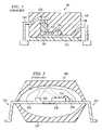
- FIG. 3is a partially fragmented side view of an embodiment of a double mold optocoupler in accordance with the present systems and methods;
- FIG. 4is a partially fragmented end view of the an embodiment of a double mold multichannel optocoupler in accordance with the present systems and methods.
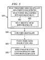
- FIG. 5is a flow chart of an embodiment of a method for forming a double mold optocoupler in accordance with the present systems and methods.
- the present systems and methodsprovide an optical device such as and optocoupler in which a clear epoxy or silicone encapsulate surrounding the LED and photodetector integrated circuit (IC) is molded or cast, rather than dispensed or deposited as is typical in the art. Casting or molding can profile the shape of the clear insulate dome more accurately, in a repeatable manner. Additionally, a lens may be fashioned or formed in the transparent encapsulate immediately above the LED and photodetector IC to maximize light coupling efficiency.
- the encapsulated componentsmay in turn be encapsulated, such as with an opaque epoxy.
- the final encapsulation epoxycan be of a reflective color, such as white, to reflect stray light from leaving the clear inner encapsulate.
- Embodiments of the present systems and methodsresult in improved light coupling between the LED and photodetector IC. As a result, not only may lower cost dimmer LEDs be used in the present optocouplers, but production yield loss due to insufficient light coupling in finished optocouplers may be decreased.
- Embodiments of the present optocouplersmay include multi-channel optocouplers, in which the inner encapsulate is molded or cast to create “walls” between LED/detector pairs to provide separate signal channels.
- Emitter 302such as may comprise any suitable light source including a LED, LASER, and the like
- detector 304such as may comprise any suitable photoelectric receiver including a photo diode, photo transistor, and the like
- leads 303 and 306extend from emitter 302 and detector 304 , respectively.
- Bond wire 305may couple detector 304 to lead 306 .
- lead configurationsmay be utilized according to the present systems and methods.
- coplanar configurations of the present systems and methodsare intended to encompass a generally coplanar configuration wherein the emitter and detector are somewhat out of the same plane in the profile, such as where one of emitter 302 and detector 304 are disposed directly upon a substrate, printed circuit board (PCB), or the like, and the other one of emitter 302 and detector 304 are disposed upon a corresponding one of leads 303 and 306 .
- PCBprinted circuit board
- double encapsulationis used to trap the light emissions from emitter 302 within light conductive or transparent inner encapsulate 309 .
- inner encapsulate 309is preferably molded around emitter 302 and detector 304 in a predetermined, repeatable shape.
- Outer opaque encapsulate 307is preferably molded around inner transparent encapsulate 309 .
- Outer opaque encapsulate 307is also preferably a reflective color, such as white.
- inner encapsulate 309may comprise an epoxy resin or silicone compound that has good optical properties, such as high Transmittance.
- embodiments of the present systems and methodsmay utilize any suitable inner encapsulate material, such as plastics, glass, various resin compounds, and the like, providing sufficient light transmittance.
- the resin comprising outer encapsulate 307is preferably comprised of an opaque lightproof resin, or the like to thereby provide protection with respect to light noise as well as physical protection of the various components of optocoupler 300 . Additionally, outer encapsulate 307 is also preferably a color which will provide reflectance within clear inner encapsulate 309 .
- outer encapsulate 307may comprise an epoxy resin having an opacifier therein which will render the outer encapsulate white.
- other materials moldablemay be utilized in providing outer encapsulate 307 , such as plastics, metals, various resin compounds, and the like, and other colors that sufficiently reflect the light of emitter 302 .
- lens 312may be used.
- an ellipsoidal optical lensmay be cast into the top surface of the inner encapsulate 309 , such as to provide a concave lens surface facing the emitter and/or detector of the optocoupler.
- Optical lens 312may be configured to maximize the reflected incidence of light and reduce the angle of incidence light (as shown by dashed lines in FIG. 3 ), achieving greater efficiencies with respect to the coupling of light between emitter and detector, and/or facilitating a lower package profile for optocoupler 300 .
- lens 312may be defined in inner encapsulate 309 using molding or casting techniques when encapsulating emitter 302 and detector 304 in inner encapsulate 309 . Additionally or alternatively, lens 312 may be formed using post-forming techniques, such as grinding, milling, polishing, et cetera, with respect to inner encapsulate 309 . Lens 312 is preferably sized and positioned to be placed in juxtaposition with the top of emitter 302 and detector 304 . Use of different ICs and different emitter/detectors in different optocoupler products may result in different lens positions and/or configurations. In short, the lens position may be dependent upon the optical characteristics of the emitter and/or the detector.
- Lens 312preferably has an ellipsoidal shape that may be determined through computer simulation studies for different optocoupler applications and emitter/detector parings or through empirical study. However, other lens shapes and configurations may be utilized, such as circular, cylindrical, anamorphic, aspheric, Fresnel, hemispheric, parabolic, spiral, et cetera, as well as combinations of any of the foregoing.
- emitter 302 and detector 304are preferably positioned on ellipse centers of lens 312 so as to make use of the particular angles of lens 312 to transmit more light to detector 304 and, thereby, improve the light coupling efficiency of optocoupler 300 .
- emitter 302 and photo diode 304are preferably positioned at equal distance from an absolute center of lens 312 .
- embodiments of the present optocouplersmay include multi-channel optocouplers 400 .
- Optocoupler 400may have a similar side view appearance in cross section as optocoupler 300 of FIG. 3 .
- multichannel optocoupler 400includes a molded inner encapsulate ( 409 ), in turn encapsulated by an opaque, preferably reflective, molded outer encapsulate ( 407 ).
- Each channelincludes a light source emitter 402 or 402 ′, such as may comprise any suitable light source including a LED, LASER, and the like, and detector 404 or 404 ′, such as may comprise any suitable photoelectric receiver including a photo diode, photo transistor, and the like, are positioned coplanar on leadframe 401 , or the like.
- This coplanar or linear configurationmay provide a relatively low profile multichannel optocoupler.
- leads 406 and 406 ′can be seen extending from detectors 404 and 404 ′, respectively. Leads from emitters 402 and 402 ′ cannot be seen in FIG.
- FIG. 4illustrates a 2-channel optocoupler, multichannel optocouplers having any number of channels are anticipated by the present systems and methods.
- lenses 412 and 412 ′may be used to optimize the coupling of light between corresponding emitter 402 and detector 404 , and/or emitter 402 ′ and detector 404 ′.
- ellipsoidal optical lenses 412 and 412 ′may be cast into the top surface of the inner encapsulate 409 , such as to provide concave lens surfaces facing the respective emitter and detector set of the multichannel optocoupler.
- lens 412 and 412 ′may be defined in inner encapsulate 409 using mold casting techniques when encapsulating emitters 402 , 402 ′ and detectors 404 , 404 ′ in inner encapsulate 409 .
- lens 412 and 412 ′may be formed using post-forming techniques, such as grinding, milling, polishing, et cetera, with respect to inner encapsulate 409 .
- Lenses 412 and 412 ′each preferably have an ellipsoidal shape.
- other lens shapes and configurationsmay be utilized, such as circular, cylindrical, anamorphic, aspheric, Fresnel, hemispheric, parabolic, spiral, et cetera, as well as combinations of any of the foregoing.
- the corresponding emitter and detector setare preferably positioned on ellipse centers of the corresponding lens so as to make use of the particular angles of the corresponding lens to focus and transmit more light to the corresponding detector and, thereby, improve the light coupling efficiency of that channel of the optocoupler and to possibly reduce light scatter to neighboring channels of the multichannel optocoupler.
- wall 415is used to isolate channels one and two.
- a wallmay be disposed between each channel emitter and detector set of a multichannel optocoupler.
- Wall 415may be formed by molding a “reverse” shape for the walls into inner encapsulate 409 , which will be filed when inner encapsulate is encapsulated by outer encapsulate 407 .
- the outer encapsulateis preferably a reflective, opaque material, wall 415 blocks light from one channel from affecting operation of a neighboring channel.
- focusing of reflected light by lenses 412 and 412 ′may enhance the isolation provided by wall(s) 415 . Isolation may be further enhanced by the shape of the walls.
- the wall length and/or thicknessmay be selected such that the shadow cast by the wall will further enhance the desired isolation.
- TIRtotal internal reflection
- a medium outside of the optical medium of the inner encapsulate 309 or 409in which an emitter and detector of an optocoupler are disposed, may be employed that has a lower index of reflection than the inner encapsulate medium.
- an air gapmay be defined between inner encapsulate 309 (or 409 ) and outer encapsulate 307 (or 407 ).
- the height of the inner encapsulate, and correspondingly the profile of the package configurationmay be established at least in part as a function of the critical angle. Synergistically, as the packaging profile is shortened, the angle of incidence becomes more acute (less than the critical angle) as desired for implementation of the TIR phenomenon. Also, mediums of various densities and other attributes may be utilized in achieving the TIR phenomenon according to the present systems and methods. For example, a medium of lesser density than air, such as helium or nitrogen, may be utilized in selecting a desired critical angle and/or to accommodate the use of an inner encapsulate medium having a density providing a reflective index of 1.0 or less.
- the critical anglemay be selected or adjusted through manipulation of the media density differences (e.g. utilizing a more dense optical media and/or utilizing a less dense medium outside the optical medium). Accordingly, optical medium height, optical medium density, and density of the medium outside of the optical medium may all be selected to provide desired optocoupler package attributes.
- the present optocoupleris formed using molding processes.
- a transparent inner encapsulateis molded about at least one emitter and at least one generally coplanar detector.
- a multichannel optocouplersuch as shown in FIG. 4 a plurality of emitter and detector sets or pairs are encapsulated at 502 and a reverse shape for a wall is molded into the inner encapsulate between each of the emitter and detector sets at 502 .
- the mold used to form the inner encapsulate at 501might also form a lens into the upper surface of the inner encapsulate above the emitter and the detector (above each of the emitter and detector sets in a multichannel optocoupler) at 503 .
- the inner encapsulateis cured and a lens may be formed into, or attached to, the inner encapsulate if not molded into the inner encapsulate at 501 .
- a lens formed into the inner encapsulate at 501may be polished or otherwise finished after curing at 505 .
- an opaque, reflective outer encapsulateis molded over the inner encapsulate.
- the outer encapsulate materialfills the reverse wall shapes of the inner encapsulate during molding at 506 , forming walls, such as wall 415 of FIG. 4 .
- the optocoupler formed light emitted from a light sourceis reflected by the reflective outer encapsulate to the corresponding detector.
Landscapes
- Physics & Mathematics (AREA)
- General Physics & Mathematics (AREA)
- Optics & Photonics (AREA)
- Photo Coupler, Interrupter, Optical-To-Optical Conversion Devices (AREA)
Abstract
Description
Claims (19)
Priority Applications (1)
| Application Number | Priority Date | Filing Date | Title |
|---|---|---|---|
| US11/205,730US7748912B2 (en) | 2002-10-29 | 2005-08-17 | Double mold optocouplers |
Applications Claiming Priority (2)
| Application Number | Priority Date | Filing Date | Title |
|---|---|---|---|
| US10/282,341US7021839B2 (en) | 2002-10-29 | 2002-10-29 | Low profile optocouplers |
| US11/205,730US7748912B2 (en) | 2002-10-29 | 2005-08-17 | Double mold optocouplers |
Related Parent Applications (1)
| Application Number | Title | Priority Date | Filing Date |
|---|---|---|---|
| US10/282,341Continuation-In-PartUS7021839B2 (en) | 2002-10-29 | 2002-10-29 | Low profile optocouplers |
Publications (2)
| Publication Number | Publication Date |
|---|---|
| US20050286840A1 US20050286840A1 (en) | 2005-12-29 |
| US7748912B2true US7748912B2 (en) | 2010-07-06 |
Family
ID=46304954
Family Applications (1)
| Application Number | Title | Priority Date | Filing Date |
|---|---|---|---|
| US11/205,730Expired - Fee RelatedUS7748912B2 (en) | 2002-10-29 | 2005-08-17 | Double mold optocouplers |
Country Status (1)
| Country | Link |
|---|---|
| US (1) | US7748912B2 (en) |
Cited By (9)
| Publication number | Priority date | Publication date | Assignee | Title |
|---|---|---|---|---|
| US20100171127A1 (en)* | 2009-01-08 | 2010-07-08 | Nec Electronics Corporation | Optically coupled device and method of manufacturing the same |
| US20110211790A1 (en)* | 2010-03-01 | 2011-09-01 | Omron Corporation | Optical coupler and producing method thereof |
| US20110235975A1 (en)* | 2010-03-23 | 2011-09-29 | Avago Technologies Ecbu Ip (Singapore) Pte. Ltd. | Optocoupler with light guide defining element |
| US20110235974A1 (en)* | 2010-03-23 | 2011-09-29 | Thiam Siew Gary Tay | Optocoupler |
| CN103065983A (en)* | 2011-10-24 | 2013-04-24 | 安华高科技Ecbuip(新加坡)私人有限公司 | Simultaneous silicone dispension on coupler |
| US8577190B2 (en) | 2010-03-23 | 2013-11-05 | Avago Technologies General Ip (Singapore) Pte. Ltd. | Optocoupler |
| US20140119691A1 (en)* | 2012-10-29 | 2014-05-01 | Avago Technologies General Ip (Singapore) Pte. Ltd. | Opto-coupler with light guide |
| US20190035966A1 (en)* | 2017-07-26 | 2019-01-31 | Anpec Electronics Corporation | Optocoupler device and frame module thereof |
| RU2752615C1 (en)* | 2021-02-01 | 2021-07-29 | федеральное государственное бюджетное образовательное учреждение высшего образования «Оренбургский государственный университет» | Optic coupler with semiconductor laser |
Families Citing this family (14)
| Publication number | Priority date | Publication date | Assignee | Title |
|---|---|---|---|---|
| DE10250540B3 (en)* | 2002-10-29 | 2004-07-15 | Infineon Technologies Ag | Process for producing an optoelectronic component |
| JP4359201B2 (en)* | 2004-07-26 | 2009-11-04 | シャープ株式会社 | Optical semiconductor device, optical connector and electronic device |
| US7909482B2 (en) | 2006-08-21 | 2011-03-22 | Innotec Corporation | Electrical device having boardless electrical component mounting arrangement |
| US7712933B2 (en) | 2007-03-19 | 2010-05-11 | Interlum, Llc | Light for vehicles |
| US8408773B2 (en) | 2007-03-19 | 2013-04-02 | Innotec Corporation | Light for vehicles |
| WO2009076579A2 (en) | 2007-12-12 | 2009-06-18 | Innotec Corporation | Overmolded circuit board and method |
| CN102401945A (en)* | 2010-09-13 | 2012-04-04 | 沈震强 | Packaging structure for improving internal transmission efficiency of photoelectric coupler |
| CN102914832A (en)* | 2011-08-05 | 2013-02-06 | 快捷半导体(苏州)有限公司 | Wafer-level molded optical coupler |
| US20130119282A1 (en) | 2011-11-14 | 2013-05-16 | Stmicroelectronics Pte Ltd. | Wafer level packaging, optical detection sensor and method of forming same |
| DE112013002944T5 (en) | 2012-06-13 | 2015-02-19 | Innotec, Corp. | Flexible hollow fiber optic cable |
| US20140161468A1 (en)* | 2012-12-07 | 2014-06-12 | General Electric Company | Optical isolation system and assembly |
| CN104465640A (en)* | 2013-09-24 | 2015-03-25 | 兆龙国际股份有限公司 | Optical coupler |
| US11038077B2 (en)* | 2018-03-05 | 2021-06-15 | Xintec Inc. | Chip package and manufacturing method thereof |
| EP3584171B1 (en) | 2018-06-19 | 2023-07-26 | Goodrich Lighting Systems GmbH | Aircraft beacon light and aircraft comprising an aircraft beacon light |
Citations (12)
| Publication number | Priority date | Publication date | Assignee | Title |
|---|---|---|---|---|
| US4614958A (en) | 1981-02-23 | 1986-09-30 | Omron Tateisi Electronics Co. | Light emitting and receiving device |
| US5056922A (en) | 1988-02-26 | 1991-10-15 | Canadian Patents And Development Limited/Societe Canadienne Des Brevets Et D'exploitation Limitee | Method and apparatus for monitoring the surface profile of a moving workpiece |
| US5150438A (en) | 1991-07-29 | 1992-09-22 | Motorola, Inc. | Optocoupler apparatus with reflective overcoat |
| US5296715A (en) | 1992-12-21 | 1994-03-22 | The United States Of America As Represented By The Department Of Energy | Optically isolated signal coupler with linear response |
| US5702775A (en) | 1995-12-26 | 1997-12-30 | Motorola, Inc. | Microelectronic device package and method |
| US5751009A (en)* | 1996-04-25 | 1998-05-12 | Motorola, Inc. | Optical isolator having leadframe with non-planar mounting portions |
| US6031251A (en) | 1993-06-07 | 2000-02-29 | Motorola, Inc. | Linear integrated optocoupler and method for forming the same |
| US6246123B1 (en)* | 1998-05-04 | 2001-06-12 | Motorola, Inc. | Transparent compound and applications for its use |
| US6306688B1 (en)* | 1999-04-28 | 2001-10-23 | Teravicta Technologies, Inc. | Method of reworkably removing a fluorinated polymer encapsulant |
| US6525386B1 (en) | 1998-03-10 | 2003-02-25 | Masimo Corporation | Non-protruding optoelectronic lens |
| US6754407B2 (en)* | 2001-06-26 | 2004-06-22 | Intel Corporation | Flip-chip package integrating optical and electrical devices and coupling to a waveguide on a board |
| US7021839B2 (en)* | 2002-10-29 | 2006-04-04 | Dominique Ho | Low profile optocouplers |
- 2005
- 2005-08-17USUS11/205,730patent/US7748912B2/ennot_activeExpired - Fee Related
Patent Citations (12)
| Publication number | Priority date | Publication date | Assignee | Title |
|---|---|---|---|---|
| US4614958A (en) | 1981-02-23 | 1986-09-30 | Omron Tateisi Electronics Co. | Light emitting and receiving device |
| US5056922A (en) | 1988-02-26 | 1991-10-15 | Canadian Patents And Development Limited/Societe Canadienne Des Brevets Et D'exploitation Limitee | Method and apparatus for monitoring the surface profile of a moving workpiece |
| US5150438A (en) | 1991-07-29 | 1992-09-22 | Motorola, Inc. | Optocoupler apparatus with reflective overcoat |
| US5296715A (en) | 1992-12-21 | 1994-03-22 | The United States Of America As Represented By The Department Of Energy | Optically isolated signal coupler with linear response |
| US6031251A (en) | 1993-06-07 | 2000-02-29 | Motorola, Inc. | Linear integrated optocoupler and method for forming the same |
| US5702775A (en) | 1995-12-26 | 1997-12-30 | Motorola, Inc. | Microelectronic device package and method |
| US5751009A (en)* | 1996-04-25 | 1998-05-12 | Motorola, Inc. | Optical isolator having leadframe with non-planar mounting portions |
| US6525386B1 (en) | 1998-03-10 | 2003-02-25 | Masimo Corporation | Non-protruding optoelectronic lens |
| US6246123B1 (en)* | 1998-05-04 | 2001-06-12 | Motorola, Inc. | Transparent compound and applications for its use |
| US6306688B1 (en)* | 1999-04-28 | 2001-10-23 | Teravicta Technologies, Inc. | Method of reworkably removing a fluorinated polymer encapsulant |
| US6754407B2 (en)* | 2001-06-26 | 2004-06-22 | Intel Corporation | Flip-chip package integrating optical and electrical devices and coupling to a waveguide on a board |
| US7021839B2 (en)* | 2002-10-29 | 2006-04-04 | Dominique Ho | Low profile optocouplers |
Non-Patent Citations (1)
| Title |
|---|
| Vishay Telefunken, "Optocouplers", Website Retrieved from: www.vishay.com/products/optoelectronics/opc.html Retrieved on: Oct. 29, 2002, 1-3. |
Cited By (15)
| Publication number | Priority date | Publication date | Assignee | Title |
|---|---|---|---|---|
| US8288183B2 (en) | 2009-01-08 | 2012-10-16 | Renesas Electronics Corporation | Method of manufacturing an optically coupled device |
| US20100171127A1 (en)* | 2009-01-08 | 2010-07-08 | Nec Electronics Corporation | Optically coupled device and method of manufacturing the same |
| US8143637B2 (en)* | 2009-01-08 | 2012-03-27 | Renesas Electronics Corporation | Optically coupled device with an optical waveguide |
| US20110211790A1 (en)* | 2010-03-01 | 2011-09-01 | Omron Corporation | Optical coupler and producing method thereof |
| US8346033B2 (en)* | 2010-03-01 | 2013-01-01 | Omron Corporation | Optical coupler and producing method thereof |
| US20110235974A1 (en)* | 2010-03-23 | 2011-09-29 | Thiam Siew Gary Tay | Optocoupler |
| US20110235975A1 (en)* | 2010-03-23 | 2011-09-29 | Avago Technologies Ecbu Ip (Singapore) Pte. Ltd. | Optocoupler with light guide defining element |
| US8412006B2 (en) | 2010-03-23 | 2013-04-02 | Avago Technologies Ecbu Ip (Singapore) Pte. Ltd. | Optocoupler |
| US8571360B2 (en)* | 2010-03-23 | 2013-10-29 | Avago Technologies General Ip (Singapore) Pte. Ltd. | Optocoupler with light guide defining element |
| US8577190B2 (en) | 2010-03-23 | 2013-11-05 | Avago Technologies General Ip (Singapore) Pte. Ltd. | Optocoupler |
| CN103065983A (en)* | 2011-10-24 | 2013-04-24 | 安华高科技Ecbuip(新加坡)私人有限公司 | Simultaneous silicone dispension on coupler |
| US20140119691A1 (en)* | 2012-10-29 | 2014-05-01 | Avago Technologies General Ip (Singapore) Pte. Ltd. | Opto-coupler with light guide |
| US20190035966A1 (en)* | 2017-07-26 | 2019-01-31 | Anpec Electronics Corporation | Optocoupler device and frame module thereof |
| US10446708B2 (en)* | 2017-07-26 | 2019-10-15 | Anpec Electronics Corporation | Optocoupler device and frame module thereof |
| RU2752615C1 (en)* | 2021-02-01 | 2021-07-29 | федеральное государственное бюджетное образовательное учреждение высшего образования «Оренбургский государственный университет» | Optic coupler with semiconductor laser |
Also Published As
| Publication number | Publication date |
|---|---|
| US20050286840A1 (en) | 2005-12-29 |
Similar Documents
| Publication | Publication Date | Title |
|---|---|---|
| US7748912B2 (en) | Double mold optocouplers | |
| US7021839B2 (en) | Low profile optocouplers | |
| US9425360B2 (en) | Light emitting device package | |
| CN100568553C (en) | Device with double curvature lens and method of designing and manufacturing the same | |
| US8089089B2 (en) | Side-emitting LED package and manufacturing method of the same | |
| KR101488448B1 (en) | LED package and manufacturing method thereof | |
| US20180212118A1 (en) | Beveled chip reflector for chip-scale packaging light-emitting device and manufacturing method of the same | |
| US8860047B2 (en) | Semiconductor light-emitting device | |
| US20090279279A1 (en) | Light emitting device and a manufacturing method thereof | |
| US8288183B2 (en) | Method of manufacturing an optically coupled device | |
| KR20130028160A (en) | Optoelectronic component with a wireless contacting | |
| CN101521194A (en) | High-speed photoelectric subassembly and flip chip structure thereof | |
| CN102859729A (en) | Optoelectronic component and method for producing an optoelectronic component | |
| US7358535B2 (en) | Photo-coupler semiconductor device and production method therefor | |
| US8757833B2 (en) | Light emitting device package | |
| CN108271423A (en) | The method of optical package and production optical package | |
| US20180182739A1 (en) | Light-emitting diode arrangement and method for the production thereof | |
| US8664681B2 (en) | Parallel plate slot emission array | |
| US20140004631A1 (en) | Method for manufcturing light emitting diode package | |
| US20150041687A1 (en) | Optical coupling device and method of manufacturing optical coupling device | |
| KR20090073598A (en) | LED Package | |
| US20150198294A1 (en) | Light bar, backlight device, and manufacturing methods thereof | |
| TW202024697A (en) | Photocoupler | |
| CN212967699U (en) | Optical sensor | |
| WO2025147842A1 (en) | Light emmitting diode package with improved light quality |
Legal Events
| Date | Code | Title | Description |
|---|---|---|---|
| AS | Assignment | Owner name:AGILENT TECHNOLOGIES, INC., COLORADO Free format text:ASSIGNMENT OF ASSIGNORS INTEREST;ASSIGNORS:HO, SOO KIANG;SIA, CHIN HIAN;TAY, THIAM SIEW GARY;AND OTHERS;REEL/FRAME:016502/0692 Effective date:20050810 | |
| AS | Assignment | Owner name:AVAGO TECHNOLOGIES GENERAL IP PTE. LTD.,SINGAPORE Free format text:ASSIGNMENT OF ASSIGNORS INTEREST;ASSIGNOR:AGILENT TECHNOLOGIES, INC.;REEL/FRAME:017206/0666 Effective date:20051201 Owner name:AVAGO TECHNOLOGIES GENERAL IP PTE. LTD., SINGAPORE Free format text:ASSIGNMENT OF ASSIGNORS INTEREST;ASSIGNOR:AGILENT TECHNOLOGIES, INC.;REEL/FRAME:017206/0666 Effective date:20051201 | |
| AS | Assignment | Owner name:AVAGO TECHNOLOGIES ECBU IP (SINGAPORE) PTE. LTD.,S Free format text:ASSIGNMENT OF ASSIGNORS INTEREST;ASSIGNOR:AVAGO TECHNOLOGIES GENERAL IP (SINGAPORE) PTE. LTD.;REEL/FRAME:017675/0626 Effective date:20051201 Owner name:AVAGO TECHNOLOGIES ECBU IP (SINGAPORE) PTE. LTD., Free format text:ASSIGNMENT OF ASSIGNORS INTEREST;ASSIGNOR:AVAGO TECHNOLOGIES GENERAL IP (SINGAPORE) PTE. LTD.;REEL/FRAME:017675/0626 Effective date:20051201 | |
| STCF | Information on status: patent grant | Free format text:PATENTED CASE | |
| FPAY | Fee payment | Year of fee payment:4 | |
| AS | Assignment | Owner name:DEUTSCHE BANK AG NEW YORK BRANCH, AS COLLATERAL AGENT, NEW YORK Free format text:PATENT SECURITY AGREEMENT;ASSIGNOR:AVAGO TECHNOLOGIES GENERAL IP (SINGAPORE) PTE. LTD.;REEL/FRAME:032851/0001 Effective date:20140506 Owner name:DEUTSCHE BANK AG NEW YORK BRANCH, AS COLLATERAL AG Free format text:PATENT SECURITY AGREEMENT;ASSIGNOR:AVAGO TECHNOLOGIES GENERAL IP (SINGAPORE) PTE. LTD.;REEL/FRAME:032851/0001 Effective date:20140506 | |
| AS | Assignment | Owner name:AVAGO TECHNOLOGIES GENERAL IP (SINGAPORE) PTE. LTD., SINGAPORE Free format text:TERMINATION AND RELEASE OF SECURITY INTEREST IN PATENT RIGHTS (RELEASES RF 032851-0001);ASSIGNOR:DEUTSCHE BANK AG NEW YORK BRANCH, AS COLLATERAL AGENT;REEL/FRAME:037689/0001 Effective date:20160201 Owner name:AVAGO TECHNOLOGIES GENERAL IP (SINGAPORE) PTE. LTD Free format text:TERMINATION AND RELEASE OF SECURITY INTEREST IN PATENT RIGHTS (RELEASES RF 032851-0001);ASSIGNOR:DEUTSCHE BANK AG NEW YORK BRANCH, AS COLLATERAL AGENT;REEL/FRAME:037689/0001 Effective date:20160201 | |
| AS | Assignment | Owner name:BANK OF AMERICA, N.A., AS COLLATERAL AGENT, NORTH CAROLINA Free format text:PATENT SECURITY AGREEMENT;ASSIGNOR:AVAGO TECHNOLOGIES GENERAL IP (SINGAPORE) PTE. LTD.;REEL/FRAME:037808/0001 Effective date:20160201 Owner name:BANK OF AMERICA, N.A., AS COLLATERAL AGENT, NORTH Free format text:PATENT SECURITY AGREEMENT;ASSIGNOR:AVAGO TECHNOLOGIES GENERAL IP (SINGAPORE) PTE. LTD.;REEL/FRAME:037808/0001 Effective date:20160201 | |
| AS | Assignment | Owner name:AVAGO TECHNOLOGIES GENERAL IP (SINGAPORE) PTE. LTD Free format text:CORRECTIVE ASSIGNMENT TO CORRECT THE ASSIGNEE NAME PREVIOUSLY RECORDED AT REEL: 017206 FRAME: 0666. ASSIGNOR(S) HEREBY CONFIRMS THE ASSIGNMENT;ASSIGNOR:AGILENT TECHNOLOGIES, INC.;REEL/FRAME:038632/0662 Effective date:20051201 | |
| AS | Assignment | Owner name:AVAGO TECHNOLOGIES GENERAL IP (SINGAPORE) PTE. LTD., SINGAPORE Free format text:TERMINATION AND RELEASE OF SECURITY INTEREST IN PATENTS;ASSIGNOR:BANK OF AMERICA, N.A., AS COLLATERAL AGENT;REEL/FRAME:041710/0001 Effective date:20170119 Owner name:AVAGO TECHNOLOGIES GENERAL IP (SINGAPORE) PTE. LTD Free format text:TERMINATION AND RELEASE OF SECURITY INTEREST IN PATENTS;ASSIGNOR:BANK OF AMERICA, N.A., AS COLLATERAL AGENT;REEL/FRAME:041710/0001 Effective date:20170119 | |
| MAFP | Maintenance fee payment | Free format text:PAYMENT OF MAINTENANCE FEE, 8TH YEAR, LARGE ENTITY (ORIGINAL EVENT CODE: M1552) Year of fee payment:8 | |
| AS | Assignment | Owner name:AVAGO TECHNOLOGIES INTERNATIONAL SALES PTE. LIMITE Free format text:MERGER;ASSIGNOR:AVAGO TECHNOLOGIES GENERAL IP (SINGAPORE) PTE. LTD.;REEL/FRAME:047196/0687 Effective date:20180509 | |
| AS | Assignment | Owner name:AVAGO TECHNOLOGIES INTERNATIONAL SALES PTE. LIMITE Free format text:CORRECTIVE ASSIGNMENT TO CORRECT THE EFFECTIVE DATE OF MERGER TO 9/5/2018 PREVIOUSLY RECORDED AT REEL: 047196 FRAME: 0687. ASSIGNOR(S) HEREBY CONFIRMS THE MERGER;ASSIGNOR:AVAGO TECHNOLOGIES GENERAL IP (SINGAPORE) PTE. LTD.;REEL/FRAME:047630/0344 Effective date:20180905 | |
| AS | Assignment | Owner name:AVAGO TECHNOLOGIES INTERNATIONAL SALES PTE. LIMITE Free format text:CORRECTIVE ASSIGNMENT TO CORRECT THE PROPERTY NUMBERS PREVIOUSLY RECORDED AT REEL: 47630 FRAME: 344. ASSIGNOR(S) HEREBY CONFIRMS THE ASSIGNMENT;ASSIGNOR:AVAGO TECHNOLOGIES GENERAL IP (SINGAPORE) PTE. LTD.;REEL/FRAME:048883/0267 Effective date:20180905 | |
| FEPP | Fee payment procedure | Free format text:MAINTENANCE FEE REMINDER MAILED (ORIGINAL EVENT CODE: REM.); ENTITY STATUS OF PATENT OWNER: LARGE ENTITY | |
| LAPS | Lapse for failure to pay maintenance fees | Free format text:PATENT EXPIRED FOR FAILURE TO PAY MAINTENANCE FEES (ORIGINAL EVENT CODE: EXP.); ENTITY STATUS OF PATENT OWNER: LARGE ENTITY | |
| STCH | Information on status: patent discontinuation | Free format text:PATENT EXPIRED DUE TO NONPAYMENT OF MAINTENANCE FEES UNDER 37 CFR 1.362 | |
| STCH | Information on status: patent discontinuation | Free format text:PATENT EXPIRED DUE TO NONPAYMENT OF MAINTENANCE FEES UNDER 37 CFR 1.362 | |
| FP | Lapsed due to failure to pay maintenance fee | Effective date:20220706 |