US7747903B2 - Error correction for memory - Google Patents
Error correction for memoryDownload PDFInfo
- Publication number
- US7747903B2 US7747903B2US11/774,825US77482507AUS7747903B2US 7747903 B2US7747903 B2US 7747903B2US 77482507 AUS77482507 AUS 77482507AUS 7747903 B2US7747903 B2US 7747903B2
- Authority
- US
- United States
- Prior art keywords
- page
- data
- memory
- error correction
- cells
- Prior art date
- Legal status (The legal status is an assumption and is not a legal conclusion. Google has not performed a legal analysis and makes no representation as to the accuracy of the status listed.)
- Active, expires
Links
Images


Classifications
- G—PHYSICS
- G06—COMPUTING OR CALCULATING; COUNTING
- G06F—ELECTRIC DIGITAL DATA PROCESSING
- G06F11/00—Error detection; Error correction; Monitoring
- G06F11/07—Responding to the occurrence of a fault, e.g. fault tolerance
- G06F11/08—Error detection or correction by redundancy in data representation, e.g. by using checking codes
- G06F11/10—Adding special bits or symbols to the coded information, e.g. parity check, casting out 9's or 11's
- G06F11/1008—Adding special bits or symbols to the coded information, e.g. parity check, casting out 9's or 11's in individual solid state devices
- G06F11/1072—Adding special bits or symbols to the coded information, e.g. parity check, casting out 9's or 11's in individual solid state devices in multilevel memories
- G—PHYSICS
- G11—INFORMATION STORAGE
- G11C—STATIC STORES
- G11C11/00—Digital stores characterised by the use of particular electric or magnetic storage elements; Storage elements therefor
- G11C11/56—Digital stores characterised by the use of particular electric or magnetic storage elements; Storage elements therefor using storage elements with more than two stable states represented by steps, e.g. of voltage, current, phase, frequency
Definitions
- Embodiments of this disclosuremay relate generally to memory devices including non-volatile memory.
- RAMrandom-access memory
- ROMread-only memory
- DRAMdynamic random access memory
- SDRAMsynchronous dynamic random access memory
- non-volatile memorynon-volatile memory
- flash memorynon-volatile memory
- Flash memory devicesmay utilize one-transistor memory cells which allow for high memory density, high reliability and low power consumption. Flash memory devices are made in two forms: NOR flash and NAND flash. NAND flash can be either of single-level cell (SLC) or multi-level cell (MLC). Memory devices can be categorized further into two broad areas as volatile and non-volatile. Volatile memory devices require power to maintain data, while non volatile memories are capable of maintaining data in the absence of a power supply. An example of a non-volatile memory is a flash memory that stores information on a semiconductor structure without the need for power to maintain the information in the chip. MLC non-volatile memory allows for higher density memory because it allows storage of two or more data bits in each memory cell.
- SLCsingle-level cell
- MLCmulti-level cell
- Memory devicescan be organized into blocks that are divided up into pages, having smaller segments, named sectors. Each sector comprises bits of information, the number of bits is determined by the density of the memory device. Memory devices may further include error correction codes to correct for data errors. Examples of error correction in memory devices can be found in U.S. Patent Application Publication Nos. 2005/0172207 and 2005/0268203, which are assigned to the present assignee and incorporated by reference.
- FIG. 1is a block diagram of a memory system, according to various embodiments of the invention.
- FIG. 2is a block diagram showing the organization of arrays of memory cells in a NAND flash memory, according to various embodiments of the invention.
- FIG. 3is a schematic diagram of a NAND flash memory array, according to various embodiments of the present invention.
- FIG. 4is a diagram showing the distribution of threshold voltages of a multi-level cell array of FIG. 3 , according to various embodiments of the present invention.
- FIG. 5is a block diagram of example data in a non volatile memory according to various embodiments of the present invention.
- FIG. 6is a flow chart of a method for determining error correction in non volatile memory according to various embodiments of the invention.
- FIG. 7is a flow chart of a method for storing error correction in non volatile memory according to various embodiments of the invention.
- FIG. 8is a flow chart of a method for reading error correction in non volatile memory according to various embodiments of the invention.
- FIG. 9is a block diagram of a system according to various embodiments of the invention.
- Error analysiscan include detection and analysis, and combinations thereof.
- Other embodimentsprovide memory structures, apparatus and/or systems with error correction.
- error correction datais stored in a memory area associated with a specific page of data to which the error correction data relate.
- multilevel cellswhich can store more than one data bit, the different bits may not have the have the same likelihood that an error will occur.
- the number of cells devoted to error correction data for the more error prone bitscan be increased and the number of cells devoted to error correction of the less error prone bits is reduced.
- FIG. 1is a simplified block diagram of a memory system 100 , according to various embodiments of the present invention.
- memory system 100includes an integrated circuit 102 having an array of non-volatile memory cells 104 , address circuitry 106 , look up table 108 , and input/output (I/O) circuitry 110 .
- Memory cells 104may be floating gate memory cells. Memory cells 104 may also be referred to as flash memory because blocks of memory cells 104 may be erased concurrently in a flash operation.
- the memory cells 104are multi-level memory cells. Multi-level memory cells store more than one bit of data per cell.
- Memory controller 114includes a processor 116 .
- the processor 116is connected to control lines 112 that communicate with the memory array 104 via integrated circuit 102 .
- Access to the memory array 104includes one or more targeted or specified memory cells linked by addressing via the control lines 112 .
- datamay be written to or read from the memory cells.
- an allocation request associated with a read requestis sent by the processor 116 , such an operation may include accessing multiple rows or pages of data to allow identification of related data contained within the memory array 104 .
- the look up table 108can translate logical addresses into physical addresses such that the bad cells or words can be readdressed and the memory array will store a certain quantity of data.
- the look up tableis in the controller 114 .
- FIG. 2is a schematic diagram showing the organization architecture of arrays of memory cells in a NAND flash memory 200 , according to various embodiments of the present invention.
- Memory 200is structured to include a plurality of blocks, e.g., block 202 , which may be representative of a portion of memory in an array similar to memory array 104 .
- a blockis composed of a plurality of pages.
- the memory 200further includes a data register 204 , a cache register 206 , a data area 208 , a spare area 210 , I/O ports 212 and a plane 214 . Data is transferred to and from the NAND flash memory 200 , byte-by-byte through the data register 204 and the cache register 206 .
- the cache register 206can be closest to I/O control circuitry, such as I/O circuitry 110 shown in FIG. 1 , and act as a data buffer for the I/O data, whereas the data register 204 can be closest to the memory array, such as memory array 104 , and act as a data buffer for the NAND flash memory array operation.
- NAND flash memoryis programmed and read in page-based operations and is erased in block-based operations.
- the data register 204 and cache register 206are tied together and act as a single register.
- the data register 204 and cache register 206operate independently to increase data throughput.
- NAND flash memory shown in FIG. 2includes blocks 202 of pages. Each block 202 is usually composed of 16, 32, or 64 pages. In an embodiment, a NAND Flash block is 128 KB. Erasing a block sets all bits to “1” (and all bytes to FFh). Programming is necessary to change erased bits from “1” to “0.” The smallest entity that can be programmed is a page. In various embodiments, each page may comprise 512 bytes (256 words) in data area 208 and an extra 16 bytes (8 words) in spare area 210 . In various embodiments, each page may have 2048 bytes (1024 words) in data area 208 and 64 bytes (32 words) in spare area 210 .
- Spare area 210may store bits used for erase block management functions, marking invalid blocks during the production process, may store logical address information used to reference partial page cache entries associated with multiple full page blocks, or store error correction data.
- the example of FIG. 2shows the I/O ports 212 as having a range of bits zero to seven (or 8 bits total) but this may vary as described with respect to page sizes above.
- the length of data area 208 and spare area 210is defined as a “page.”
- the spare area 210has significantly fewer memory cells than the data area 208 .
- the spare area 208has sixty four bytes and the data area has two kilobytes of data area. Stated another way the spare area is about three percent (3.125%) the size of the data area.
- the data area for each row of memory cellscan be divided into four sectors and the spare area includes four separate error correction data segments, one for each data sector. Accordingly, there can be up to 16 bytes in the spare area per 512-byte sector in the data area.
- a multilevel cell operationcan include two passes to program the multilevel cell.
- An allocation request associated with a read or write operation to transfer informationtakes place on a page basis (e.g., 528 bytes at a time, as opposed to a byte or word basis that is performed in a NOR flash.) Additionally, the erase operation takes place on a block basis.
- a page of 528 bytesis transferred from memory into the data register 204 .
- a page write operationa page of 528 bytes is written into the data register 204 and then programmed into the memory array 104 , such as within the space comprising data area 208 .
- a block erase operationa group of consecutive pages is erased in a single operation.
- FIG. 3is a schematic diagram of a non-volatile flash memory array 300 , according to various embodiments of the present invention.
- An example, of non-volatile memoryis NAND flash memory.
- Memory array 300shows that the number of bit lines (BL 1 , BL 2 -BL n ) within a block determines the size of a page. The size of a memory chip is determined by the number of strings allocated to each bit line, i.e., the number of blocks determines the size of a memory chips.
- the memory array 300includes an array of floating gate memory cells 321 - 326 arranged in series string 320 . Each floating gate memory cell is to store an energy level that represents more than one bit for a multilevel cell application.
- Each of the floating gate memory cells 321 - 326is connected drain to source, in a series string, such that the drain of the first floating gate memory cell 321 attaches to first bit line BL 1 through first drain select gate 327 .
- the state of the first drain select gate 327is controlled by drain select gate control line SG(D) 319 .
- the arrangement of the series string 320includes the last floating gate memory cell 326 attached to the first bit line BL 1 through first source select gate 328 and controlled by source select gate control line SG(S) 329 .
- a similar arrangementoccurs in the second series string 330 and final series string 340 such that the final series string 340 may determine the memory density of the array. As such, similar elements are labeled in a similar manner.
- the second series string 330includes an array of floating gate memory cells 331 - 336 , connected drain to source, having the first drain memory cell 331 attached to second bit line BL 2 through second drain select gate 337 , and is controlled by drain select gate control line SG(D) 319 .
- the last memory cell 336 of the second series string 330attaches to the second bit line BL 2 through second source select gate 338 , and is controlled by source select gate control line SG(S) 329 .
- Word-linesthat span across multiple series strings 320 , 330 and 340 may be coupled to the control gates of every floating gate memory cell in a given row to control their operation.
- the first word line WL 0 350couples to each first floating gate memory cell 321 , 331 and 341 of bit lines BL 1 , BL 2 and BL n .
- Each bit line BL 1 -BL neventually couples to sense amplifiers (not shown) that detect the state of each cell.
- WL 0 -WL 31may select the individual floating gate memory cells in the series strings 320 , 330 and 340 to be written to or read from and operate the remaining floating gate memory cells in each series string 320 , 330 and 340 in a pass-through mode.
- Each floating gate memory cellcan be programmed using a single bit per cell or multiple bits per cell.
- Single-level cellsallow programming a single bit per cell.
- Multi-levelallow for programming multiple bits per cell. In an example, one bit is programmed per pass and thus programming multilevel cells can have an equal number of programming passes as the number of bits that can be programmed.
- Each floating gate memory cell's threshold voltagedetermines the data that is stored in the cell. For example, in a single bit per cell architecture, a V t of 1V might indicate a programmed cell while a V t of ⁇ 1V might indicate an erased cell.
- the multi-level cellshave more than two V t values that each indicates a different state.
- V t valuesare the center of a distribution or range of values that can represent data stored in the multi-level cell. In an example, this distribution may be +/ ⁇ 0.1 V about V t .
- Multilevel floating gate memory cellstake advantage of the analog nature of a traditional flash cell by assigning a bit pattern to a specific voltage range stored on the cell. This technology permits the storage of two or more bits per cell, depending on the number of voltage ranges assigned to the cell.
- a floating gate memory cellmay be assigned four different voltage V t distributions having a width of approximately 200 milivolts (mV).
- mVmilivolts
- a separation of 0.3V to 0.5Vis assigned between each V t distribution as well. This separation zone between the V t distributions may reduce the chance that the multiple V t distributions do not overlap, which can lead to logic errors and/or data errors.
- Programming of selected floating gate memory cells within a selected WLmay be accomplished by sinking the BL to 0V. This results in a potential formed across the channel, and the WL will cause the floating gate memory cell to program. The V t will increase as higher programming pulses are applied. Between each programming pulse, a verification phase is performed in which the selected WL is lowered to 0V, the unselected WLs are lowered to 5V and the state of the selected WL is detected. If the floating gate memory cell contains a V t sufficient to prevent conduction of the device with 0V on the WL, it is deemed to be programmed, otherwise it is deemed to be still erased and the programming pulse height is increased by 0.5V and again applied to the selected WL. This process is repeated until all selected WLs are detected as being programmed.
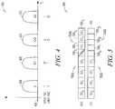
- FIG. 4is a diagram showing the distribution of threshold voltages of a multi-level cell array of FIG. 3 , according to various embodiments of the present invention.
- the X-axis 404represents threshold voltages (V t ) from lowest threshold 406 to intermediate thresholds 408 , 410 to highest threshold 412 .
- programmingbegins with the highest threshold 412 performed first on the associated WL in decreasing order of threshold voltages, as the lowest threshold 406 represents an erased state.
- the erased state, or lowest threshold 406indicates a logical “11” since both bits of the multi-layer cell are in a “1” state when erased. It should be noted that, alternatively, some memory devices may indicate an erased state with a logical “0” on each bit.
- the highest threshold 412is the first programmed threshold. This places the highest voltage on the WL prior to all lower multi-level distributions being programmed, which reduces the chance of disturb conditions with other cells on the same WL that are planned to be programmed at lower V t distributions.
- all the cells in a page that may need to be programmed with bits having the highest threshold 412are programmed first.
- the next highest threshold 410may be programmed next, followed by the next to lowest threshold 408 , and then the lowest threshold 406 . These programming operations may be accomplished with consecutive programming and verification pulses where two verification pulses with two different levels are applied (i.e., 2V for “01,” and 1.3V for “00”) between every increasing programming pulse. This procedure may repeat for each data bit within each sector of a page when attempting to fill a data block.
- the bits in a blockare all erased to the lowest state, e.g., state 406 “11” as shown in FIG. 4 .
- Program operationsare performed to shift the cells where the most significant bit, i.e., upper page bit, are shifted to zero—states 408 and 410 in FIG. 4 .
- the least significant biti.e., the lower page bit, can be programmed into the appropriate cells.
- the statechanged from lowest state 406 to highest state 412 if the upper page bit remains a “1” or the state changes from state 408 to 410 if the upper page bit is a “0.”
- These programming operationsare performed by a series of charge pulses addressed to the appropriate cell, followed by verify operations.
- the data stored in multi-level cellsis not read sequentially cell-by-cell. Instead, the cells in a row are read with the digit placement representing a page of data. That is, the most significant bits in the row of cells represent a page of data and the least significant bits in the row of cells represent a different page of data. If the multi-level cells store more than two bits, then the intermediate digit positions would represent their own pages of data. Referring again to FIG. 4 , and assuming that sequential cells store the thresholds as shown, then the most significant bit page (upper page) is 0110 and the least significant bit page (lower page) is 0011.
- the most significant bit (upper) pageis more likely to have errors than the least significant bit (lower) page.
- the upper page bittransitions state between thresholds 406 and 408 .
- the upper page bitalso transitions state between thresholds 410 and 412 .
- the lower pageonly transitions state between thresholds 408 and 410 . As a result, it is twice as likely to have an error in the upper page. It would be more effective for error correction if an increased quantity of error correction was applied to the more likely error.
- FIG. 5is a block diagram of a data structure 500 that can be stored in a row of a multi-level memory cell memory.
- data structure 500is one row of the data area 208 shown in FIG. 2 .
- Data structure 500shows a memory storage area 502 A, 502 B and a spare area 504 A, 504 B for each of the most significant bit (MSB) page (suffix A) and the least significant bit (LSB) page (suffix B).
- Memory storage areas 502 A and 502 Bare to store data for an application.
- the datamay be processed or sensed data, such as image sensed data from a processor, e.g., processor 116 of FIG. 1 .
- the storage areas 502 A and 502 Binclude a plurality of sectors SEC 0 , SEC 1 , SEC 2 , SEC 3 , which respectively include a plurality of memory cells to store bits. While shown as four sectors, it will be understood that other even numbers of sectors may be used.
- the stored energy level in an individual multilevel memory cellrepresents a most significant bit (MSB) and a least significant bit (LSB). It will be recognized that the present description is extendable to numbers of bits greater than two. However, the present description discusses a two bit multi-level memory for ease of description and understanding.
- the sectorsare consecutive in the memory area.
- the sectors SEC 0 , SEC 1 , SEC 2 , SEC 3are formed by the same number of cells in each sector.
- each sectorincludes a same number of memory cells and bits for both the most significant bit and least significant bit levels of the data.
- the sectorsare an even division of the number of memory storage cells in a row.
- An example size of the sectorsis 512 kbytes.
- the spare areas 504 A and 504 Bare appended to the respective memory storage area 502 A and 502 B and provide memory storage for so called housekeeping functions associated with the memory.
- the spare areas 504 A and 504 Bcan be positioned at the beginning of a row, i.e., the “0” position or at the end of a row “N” position. Some housekeeping functions include error correction and block management.
- the spare areas 504 A and 504 Bare smaller than the data storage areas 502 A and 502 B.
- the spare area 504 A corresponding to the upper pageis evenly divided into four segments 505 0 , 505 1 , 505 2 , and 505 3 .
- the MSB pageincludes error correction data ECC 0 , ECC 1 , ECC 3 , ECC 4 that respectively corresponds to sectors SEC 0 , SEC 1 , SEC 2 , SEC 3 in the MSB page.
- the lower (LSB) page as shownincludes more than four segments 506 0 , 506 1 , 506 2 , 506 3 , and 508 .
- the LSB pageincludes error correction data in each of segments 506 0 , 506 1 , 506 2 , 506 3 that corresponds to a respective sector SEC 0 , SEC 1 , SEC 2 , SEC 3 in the LSB page.
- the number of memory cells used for each of the segments 505 of MSB pageis larger than the number of memory cells used for each of the segments 506 and 508 of the LSB page.
- the error correction data segments 505 0 , 505 1 , 505 2 , and 505 3include more bits than the error correction code segments 506 0 , 506 1 , 506 2 , 506 3 . This, in some embodiments, is based on a determination that the most significant bit page is more likely to have an error than the least significant bit page.
- the MSB pageincludes more bytes for error correction in the error correction data ECC 0 , ECC 1 , ECC 3 , ECC 4 than the corresponding error correction data ECC 0 , ECC 1 , ECC 3 , ECC 4 for the LSB level.
- the spare area 504 B for the LSB pagefurther includes block management data segment 508 .
- the MSB page error correctionuses the entirety of its spare area for only error correction in an embodiment.
- Segment 508can store memory management data, such as erase block management data, wear-leveling data, and/or logic-to-physical block mapping data.
- each row of a memory arrayhas 64 bytes in the spare area.
- For the page that is determined to have the most likely chance at error, its spare areais dedicated entirely to error correction.
- the spare area corresponding to the other pageincludes both error correction data and the block management data.
- the data in the spare areacan be set as follows. The most error prone page is set to have four sectors. Then this page includes 16 bytes of error correction data for each of the four sectors for a total of 64 bytes.
- the less error prone pagealso stores the block management data in its spare area so it can not mirror the layout of the most error prone page.
- a set number of bytesis dedicated to the block management. The remaining bytes are divided by the number of sectors.
- the block management for both pagescan be set at 16 bytes and stored in the spare area of the less error prone page, leaving 48 bytes remaining for error correction for the less error prone page.
- each of the four sectorsis associated with 12 bytes of error correction data in the spare area.
- additional error correction datacan be stored for the more error prone page. This may increase at least one of reliability and error correction of the data stored in the multi-level memory.
- the spare areacan further be set so that some error correction data, such as check data, for one page is stored in the adjacent page.
- some error correction datasuch as check data
- the less error prone pagestores error correction data for both itself and its more error prone companion page. Both pages would be read to acquire the error correction data, such as error correction codes, for the more error prone page.
- the more error-prone pageincludes a 16-bytes per sector of error correction data, such as check data, while the less error-prone page has 12-bytes per sector of error correction data. If analysis of the flash failure mechanisms leads one to believe that that this allocation is not appropriate, for example, some of the 48 bytes on the less error-prone page can be use for more error-prone page error correction data.
- Each sector on the more error-prone pagecould, as an example, be assigned an 18-bytes per sector error correction utilizing some of the bytes in the spare area corresponding to the less error-prone page to provide one of the segments, leaving the less error-prone page would then be left with 10-bytes per sector segment for its error correction data.
- the error correction data stored in the ECC of the spare areamay be coded in accordance with various error correction codes, which can also be referred to as “check bytes”.
- error correction codeswhich can also be referred to as “check bytes”.
- One exampleis Reed-Solomon code data.
- Another exampleis BCH code data.
- Other types of error correction datainclude, but are not limited to Hamming code, Reed-Muller code, and forward error correction code.
- FIG. 6is a flow chart of a method for setting the error correction arrangement for a non-volatile memory, 600 .
- a determinationis made as to the likelihood of an error occurring in each page of data stored in a single row of multi-level memory cells. This can be based at least partly on the assignment of bit patterns to a respective threshold voltage range. The bit pattern may require that the most significant bit change state more than the least significant bit. One example of this bit pattern is shown in FIG. 4 . In another embodiment, the least significant bit may change value more than the most significant bit.
- the less error prone pageis determined, then the less error prone page is flagged to store the block management data, 604 .
- the error correction data size for each pageis set.
- the spare area for the more error prone pagecan be completely dedicated to error correction data.
- the spare area of the less error prone pagealso includes error correction data but has a fewer number of bits allocated for this than the more error prone page.
- the spare area of the less error prone pagereserves a set number of bits, for example, at the end of the spare area, for the block management data, 608 . The remaining spare area is then used for error correction of the less error prone page.
- FIG. 7is a flow chart of a method for programming for a non-volatile memory, 700 .
- the data to be storedis received, 702 .
- an ECC unitwhich can be part of a controller 114 or a processor 116 , calculates the ECC data based on the received data to be stored in the sector, 702 .
- Writeable blocks of data including the error correction dataare formatted or built, 706 . Only error correction data is to be written in the spare area of the more error prone page. Both error correction data and management data are to be written to the spare area of the less error prone page.
- the ECC data for each data pageis then written to the corresponding spare area along with actual data being written to the data area, 708 . Examples of building data for writing to a non-volatile memory are described in application Ser. Nos. 11/698,456; 11/698,455; and 11/672,076, each of which is incorporated by reference for any purpose.
- FIG. 8is a flow chart of a method for reading data from a multi-level memory, 800 .
- datais read from the multi-level memory.
- the read dataincludes both pages of data, error correction data and the block management data stored within the row of multi-level cells.
- the upper page data and the lower page dataare separated, 804 .
- the error correction datais read for each of the lower page and upper page, which data will have a different number of bits for each page. The more error prone page will have a greater number of error correction bits.
- the block management datais separated from the error correction data of the less error prone page.
- the ECC datais also read out, accordingly, an error correction operation is applied to check that the data is correct, 810 .
- an ECC algorithmcan correct data errors and apply different error correction strengths to each page based on the relative error likelihood between the pages.
- the number of data errors that can be correcteddepends on the correction strength of the algorithm used.
- the ECC algorithmcan be implanted in hardware or software. Simple Hamming codes provide the easiest hardware implementation. However, they can correct only single-bit errors. Hamming typically requires 13 bits per sector. Reed-Solomon codes can provide more robust error correction capability. Reed-Solomon require multiples of 18 bits per sector to perform error correction. BCH codes can provide error correction with improved efficiency over Reed-Solomon codes. BCH requires multiples of 13 bits to perform error correction.
- FIG. 9is a block diagram of a system 900 according to various embodiments of the invention.
- the system 900includes one or more apparatus, which may be similar to or identical to that of memory system 100 in FIG. 1 .
- the system 900in some embodiments, includes a processor 916 coupled to a display 918 and/or a wireless transceiver 920 .
- the memory system 100 included in the apparatus 900 and comprising a plurality of memory cellsmay also be operatively coupled to the processor 916 .
- the system 900includes a camera 922 with including a lens 924 and an imaging plane 926 coupled to the processor 916 .
- the imaging plane 926receives light rays 928 captured by the lens 924 .
- the system 900includes an audio and or a video media player 930 , including a set of media playback controls 932 , coupled to the processor 916 .
- the system 900includes a modem 934 , a DRAM device 936 , and a non-volatile flash memory device 940 , all coupled to the processor 916 .
- the size of memory arrays, page blocks, pages and sectorsmay vary as defined by the memory device. Further, the available bytes in a spare area also vary depending on the particular memory device. Accordingly, the present disclosure is not limited to a specific size of memory unless so claimed.
- the present disclosuredescribed structures and methods to compensate for different levels of defect rates in multi-level cell memories.
- the more error prone or “at-risk” pageis subject to a more powerful error correction through the application of a greater amount of error correction data.
- the block management informationis moved to the less error prone page.
- the error correction codescan be varied to potentially be more effective.
- inventive subject mattermay be referred to herein individually or collectively by the term “invention” merely for convenience and without intending to voluntarily limit the scope of this application to any single invention or inventive concept, if more than one is in fact disclosed.
- inventive conceptany arrangement calculated to achieve the same purpose may be substituted for the specific embodiments shown.
- This disclosureis intended to cover any and all adaptations or variations of various embodiments.
Landscapes
- Engineering & Computer Science (AREA)
- Theoretical Computer Science (AREA)
- Quality & Reliability (AREA)
- Physics & Mathematics (AREA)
- General Engineering & Computer Science (AREA)
- General Physics & Mathematics (AREA)
- Computer Hardware Design (AREA)
- Read Only Memory (AREA)
- Techniques For Improving Reliability Of Storages (AREA)
- For Increasing The Reliability Of Semiconductor Memories (AREA)
Abstract
Description
Claims (28)
Priority Applications (6)
| Application Number | Priority Date | Filing Date | Title |
|---|---|---|---|
| US11/774,825US7747903B2 (en) | 2007-07-09 | 2007-07-09 | Error correction for memory |
| TW097126019ATWI394167B (en) | 2007-07-09 | 2008-07-09 | Error correction for memory |
| PCT/US2008/008436WO2009009076A2 (en) | 2007-07-09 | 2008-07-09 | Error correction for memory |
| KR1020107002788AKR101371830B1 (en) | 2007-07-09 | 2008-07-09 | Error correction for memory |
| CN200880102644.4ACN101779194B (en) | 2007-07-09 | 2008-07-09 | Error correction for memory |
| US12/823,716US7996727B2 (en) | 2007-07-09 | 2010-06-25 | Error correction for memory |
Applications Claiming Priority (1)
| Application Number | Priority Date | Filing Date | Title |
|---|---|---|---|
| US11/774,825US7747903B2 (en) | 2007-07-09 | 2007-07-09 | Error correction for memory |
Related Child Applications (1)
| Application Number | Title | Priority Date | Filing Date |
|---|---|---|---|
| US12/823,716ContinuationUS7996727B2 (en) | 2007-07-09 | 2010-06-25 | Error correction for memory |
Publications (2)
| Publication Number | Publication Date |
|---|---|
| US20090019321A1 US20090019321A1 (en) | 2009-01-15 |
| US7747903B2true US7747903B2 (en) | 2010-06-29 |
Family
ID=40229346
Family Applications (2)
| Application Number | Title | Priority Date | Filing Date |
|---|---|---|---|
| US11/774,825Active2028-06-14US7747903B2 (en) | 2007-07-09 | 2007-07-09 | Error correction for memory |
| US12/823,716ActiveUS7996727B2 (en) | 2007-07-09 | 2010-06-25 | Error correction for memory |
Family Applications After (1)
| Application Number | Title | Priority Date | Filing Date |
|---|---|---|---|
| US12/823,716ActiveUS7996727B2 (en) | 2007-07-09 | 2010-06-25 | Error correction for memory |
Country Status (5)
| Country | Link |
|---|---|
| US (2) | US7747903B2 (en) |
| KR (1) | KR101371830B1 (en) |
| CN (1) | CN101779194B (en) |
| TW (1) | TWI394167B (en) |
| WO (1) | WO2009009076A2 (en) |
Cited By (7)
| Publication number | Priority date | Publication date | Assignee | Title |
|---|---|---|---|---|
| US20090013223A1 (en)* | 2007-07-02 | 2009-01-08 | Lam Chung H | Multi-bit error correction scheme in multi-level memory storage system |
| US20110078541A1 (en)* | 2009-09-25 | 2011-03-31 | A-Data Technology (Suzhou) Co., Ltd. | Storage device and data process method |
| US7979774B1 (en)* | 2006-05-08 | 2011-07-12 | Marvell International, Ltd. | Error correction coding for varying quality channels |
| US7996727B2 (en) | 2007-07-09 | 2011-08-09 | Micron Technology, Inc. | Error correction for memory |
| US8209580B1 (en) | 2006-05-08 | 2012-06-26 | Marvell International Ltd. | Error correction coding for varying signal-to-noise ratio channels |
| WO2012106255A1 (en)* | 2011-01-31 | 2012-08-09 | Marvell World Trade Ltd. | Mapping data to non-volatile memory |
| US8806297B2 (en)* | 2011-02-08 | 2014-08-12 | Sandisk Technologies Inc. | Data recovery using additional error correction coding data |
Families Citing this family (79)
| Publication number | Priority date | Publication date | Assignee | Title |
|---|---|---|---|---|
| EP2003569B1 (en)* | 2006-03-13 | 2010-06-02 | Panasonic Corporation | Flash memory controller |
| TWI382422B (en)* | 2008-07-11 | 2013-01-11 | Genesys Logic Inc | Storage device for refreshing data pages of flash memory based on error correction code and method for the same |
| KR20100012605A (en)* | 2008-07-29 | 2010-02-08 | 삼성전자주식회사 | Non-volatile memory device and method for program using ecc |
| US8555143B2 (en)* | 2008-12-22 | 2013-10-08 | Industrial Technology Research Institute | Flash memory controller and the method thereof |
| US8386883B2 (en)* | 2009-02-24 | 2013-02-26 | International Business Machines Corporation | Lengthening life of a limited life memory |
| US20110035540A1 (en)* | 2009-08-10 | 2011-02-10 | Adtron, Inc. | Flash blade system architecture and method |
| US8077515B2 (en) | 2009-08-25 | 2011-12-13 | Micron Technology, Inc. | Methods, devices, and systems for dealing with threshold voltage change in memory devices |
| US8271697B2 (en) | 2009-09-29 | 2012-09-18 | Micron Technology, Inc. | State change in systems having devices coupled in a chained configuration |
| US8589766B2 (en)* | 2010-02-24 | 2013-11-19 | Apple Inc. | Codeword remapping schemes for non-volatile memories |
| JP5017407B2 (en) | 2010-03-24 | 2012-09-05 | 株式会社東芝 | Semiconductor memory device |
| US8429391B2 (en) | 2010-04-16 | 2013-04-23 | Micron Technology, Inc. | Boot partitions in memory devices and systems |
| US8451664B2 (en) | 2010-05-12 | 2013-05-28 | Micron Technology, Inc. | Determining and using soft data in memory devices and systems |
| US8990660B2 (en)* | 2010-09-13 | 2015-03-24 | Freescale Semiconductor, Inc. | Data processing system having end-to-end error correction and method therefor |
| CN102419734B (en)* | 2010-09-27 | 2016-05-11 | 北京中星微电子有限公司 | A kind of method of data storage and device |
| US8909851B2 (en) | 2011-02-08 | 2014-12-09 | SMART Storage Systems, Inc. | Storage control system with change logging mechanism and method of operation thereof |
| US8935466B2 (en)* | 2011-03-28 | 2015-01-13 | SMART Storage Systems, Inc. | Data storage system with non-volatile memory and method of operation thereof |
| CN102279803A (en)* | 2011-04-13 | 2011-12-14 | 西安交通大学 | Spare area distribution method for enhancing storage reliability of multilayer unit NAND-Flash |
| US8732557B2 (en) | 2011-05-31 | 2014-05-20 | Micron Technology, Inc. | Data protection across multiple memory blocks |
| US8990657B2 (en) | 2011-06-14 | 2015-03-24 | Freescale Semiconductor, Inc. | Selective masking for error correction |
| US9098399B2 (en) | 2011-08-31 | 2015-08-04 | SMART Storage Systems, Inc. | Electronic system with storage management mechanism and method of operation thereof |
| US9063844B2 (en) | 2011-09-02 | 2015-06-23 | SMART Storage Systems, Inc. | Non-volatile memory management system with time measure mechanism and method of operation thereof |
| US9021319B2 (en) | 2011-09-02 | 2015-04-28 | SMART Storage Systems, Inc. | Non-volatile memory management system with load leveling and method of operation thereof |
| US9021231B2 (en) | 2011-09-02 | 2015-04-28 | SMART Storage Systems, Inc. | Storage control system with write amplification control mechanism and method of operation thereof |
| US9588883B2 (en)* | 2011-09-23 | 2017-03-07 | Conversant Intellectual Property Management Inc. | Flash memory system |
| US9239781B2 (en) | 2012-02-07 | 2016-01-19 | SMART Storage Systems, Inc. | Storage control system with erase block mechanism and method of operation thereof |
| US8954825B2 (en) | 2012-03-06 | 2015-02-10 | Micron Technology, Inc. | Apparatuses and methods including error correction code organization |
| US9298252B2 (en) | 2012-04-17 | 2016-03-29 | SMART Storage Systems, Inc. | Storage control system with power down mechanism and method of operation thereof |
| CN104246898B (en)* | 2012-05-31 | 2017-03-22 | 慧与发展有限责任合伙企业 | local error detection and global error correction |
| US8949689B2 (en) | 2012-06-11 | 2015-02-03 | SMART Storage Systems, Inc. | Storage control system with data management mechanism and method of operation thereof |
| KR101979734B1 (en) | 2012-08-07 | 2019-05-17 | 삼성전자 주식회사 | Method for controlling a read voltage of memory device and data read operating method using method thereof |
| KR101419335B1 (en)* | 2012-11-23 | 2014-07-16 | 한양대학교 산학협력단 | Apparatus and method for page unit clustering of multi level cell flash memory |
| US9671962B2 (en) | 2012-11-30 | 2017-06-06 | Sandisk Technologies Llc | Storage control system with data management mechanism of parity and method of operation thereof |
| US9059736B2 (en) | 2012-12-03 | 2015-06-16 | Western Digital Technologies, Inc. | Methods, solid state drive controllers and data storage devices having a runtime variable raid protection scheme |
| US9123445B2 (en) | 2013-01-22 | 2015-09-01 | SMART Storage Systems, Inc. | Storage control system with data management mechanism and method of operation thereof |
| CN105103235B (en) | 2013-01-31 | 2020-03-10 | 慧与发展有限责任合伙企业 | Non-volatile multi-level cell memory with decoupled bits for higher performance and energy efficiency |
| US9214965B2 (en) | 2013-02-20 | 2015-12-15 | Sandisk Enterprise Ip Llc | Method and system for improving data integrity in non-volatile storage |
| US9329928B2 (en) | 2013-02-20 | 2016-05-03 | Sandisk Enterprise IP LLC. | Bandwidth optimization in a non-volatile memory system |
| US9183137B2 (en) | 2013-02-27 | 2015-11-10 | SMART Storage Systems, Inc. | Storage control system with data management mechanism and method of operation thereof |
| US9470720B2 (en) | 2013-03-08 | 2016-10-18 | Sandisk Technologies Llc | Test system with localized heating and method of manufacture thereof |
| US9043780B2 (en) | 2013-03-27 | 2015-05-26 | SMART Storage Systems, Inc. | Electronic system with system modification control mechanism and method of operation thereof |
| US10049037B2 (en) | 2013-04-05 | 2018-08-14 | Sandisk Enterprise Ip Llc | Data management in a storage system |
| US9170941B2 (en) | 2013-04-05 | 2015-10-27 | Sandisk Enterprises IP LLC | Data hardening in a storage system |
| US9543025B2 (en) | 2013-04-11 | 2017-01-10 | Sandisk Technologies Llc | Storage control system with power-off time estimation mechanism and method of operation thereof |
| US10546648B2 (en) | 2013-04-12 | 2020-01-28 | Sandisk Technologies Llc | Storage control system with data management mechanism and method of operation thereof |
| TWI502601B (en)* | 2013-04-24 | 2015-10-01 | Ind Tech Res Inst | Hybrid error repair method and memory apparatus thereof |
| US9898056B2 (en) | 2013-06-19 | 2018-02-20 | Sandisk Technologies Llc | Electronic assembly with thermal channel and method of manufacture thereof |
| US9313874B2 (en) | 2013-06-19 | 2016-04-12 | SMART Storage Systems, Inc. | Electronic system with heat extraction and method of manufacture thereof |
| US9244519B1 (en) | 2013-06-25 | 2016-01-26 | Smart Storage Systems. Inc. | Storage system with data transfer rate adjustment for power throttling |
| US9367353B1 (en) | 2013-06-25 | 2016-06-14 | Sandisk Technologies Inc. | Storage control system with power throttling mechanism and method of operation thereof |
| US9146850B2 (en) | 2013-08-01 | 2015-09-29 | SMART Storage Systems, Inc. | Data storage system with dynamic read threshold mechanism and method of operation thereof |
| US9361222B2 (en) | 2013-08-07 | 2016-06-07 | SMART Storage Systems, Inc. | Electronic system with storage drive life estimation mechanism and method of operation thereof |
| US9431113B2 (en) | 2013-08-07 | 2016-08-30 | Sandisk Technologies Llc | Data storage system with dynamic erase block grouping mechanism and method of operation thereof |
| US9448946B2 (en) | 2013-08-07 | 2016-09-20 | Sandisk Technologies Llc | Data storage system with stale data mechanism and method of operation thereof |
| US9152555B2 (en) | 2013-11-15 | 2015-10-06 | Sandisk Enterprise IP LLC. | Data management with modular erase in a data storage system |
| US20150161001A1 (en)* | 2013-12-06 | 2015-06-11 | Western Digital Technologies, Inc. | Misprogramming prevention in solid-state memory |
| US10417090B2 (en)* | 2013-12-23 | 2019-09-17 | Cnex Labs, Inc. | Computing system with data protection mechanism and method of operation thereof |
| CN106104491A (en)* | 2014-03-01 | 2016-11-09 | 希耐克斯实验室公司 | There is calculating system and the operational approach thereof of data protection schemes |
| US9405624B2 (en)* | 2014-06-19 | 2016-08-02 | Seagate Technology Llc | On-die error detection and correction during multi-step programming |
| US9213602B1 (en) | 2014-06-23 | 2015-12-15 | Seagate Technology Llc | Write mapping to mitigate hard errors via soft-decision decoding |
| US9558066B2 (en)* | 2014-09-26 | 2017-01-31 | Intel Corporation | Exchanging ECC metadata between memory and host system |
| TWI556254B (en)* | 2014-10-14 | 2016-11-01 | 慧榮科技股份有限公司 | Data storage device and data accessing method thereof |
| TWI555028B (en)* | 2015-02-12 | 2016-10-21 | 慧榮科技股份有限公司 | Data storage device and error correction method |
| US9786386B2 (en)* | 2015-02-27 | 2017-10-10 | Microsoft Technology Licensing, Llc | Dynamic approximate storage for custom applications |
| US9690656B2 (en)* | 2015-02-27 | 2017-06-27 | Microsoft Technology Licensing, Llc | Data encoding on single-level and variable multi-level cell storage |
| WO2016144291A1 (en)* | 2015-03-06 | 2016-09-15 | Hewlett Packard Enterprise Development Lp | Data write to subset of memory devices |
| CN106297881B (en)* | 2015-05-27 | 2020-09-11 | 旺宏电子股份有限公司 | Health management of non-volatile memory |
| US9679661B1 (en) | 2016-06-28 | 2017-06-13 | Sandisk Technologies Llc | Non-volatile storage system with self-test for read performance enhancement feature setup |
| DE102016115272A1 (en) | 2016-08-17 | 2018-02-22 | Infineon Technologies Ag | MEMORY WITH DIFFERENT RELIABILITIES |
| US9672940B1 (en) | 2016-08-18 | 2017-06-06 | Sandisk Technologies Llc | Non-volatile memory with fast read process |
| US10613924B2 (en) | 2017-05-17 | 2020-04-07 | Rambus Inc. | Energy-efficient error-correction-detection storage |
| GB201710839D0 (en)* | 2017-07-05 | 2017-08-16 | Irdeto Bv | Data protection |
| US10719398B1 (en)* | 2017-07-18 | 2020-07-21 | EMC IP Holding Company LLC | Resilience of data storage systems by managing partial failures of solid state drives |
| US10269422B2 (en)* | 2017-09-08 | 2019-04-23 | Cnex Labs, Inc. | Storage system with data reliability mechanism and method of operation thereof |
| US11190217B2 (en) | 2018-08-23 | 2021-11-30 | Phison Electronics Corp. | Data writing method, memory controlling circuit unit and memory storage device |
| TWI658463B (en)* | 2018-08-23 | 2019-05-01 | 群聯電子股份有限公司 | Data access method,memory control circuit unit and memory storage device |
| CN109446157B (en)* | 2018-10-18 | 2021-10-29 | 武汉虹旭信息技术有限责任公司 | A data format checking system and method based on formatted data |
| DE102020120719A1 (en) | 2020-08-05 | 2022-02-10 | Infineon Technologies Ag | ACCESSING A STORAGE |
| US11798647B2 (en) | 2022-02-28 | 2023-10-24 | Micron Technology, Inc. | Apparatus and methods for determining memory cell data states |
| CN119068968B (en)* | 2024-11-05 | 2025-01-17 | 湖北长江万润半导体技术有限公司 | A method for quickly testing flash memory using flash memory weak pages and their distribution types |
Citations (33)
| Publication number | Priority date | Publication date | Assignee | Title |
|---|---|---|---|---|
| US4701884A (en) | 1985-08-16 | 1987-10-20 | Hitachi, Ltd. | Semiconductor memory for serial data access |
| US4716566A (en) | 1984-08-20 | 1987-12-29 | Nec Corporation | Error correcting system |
| US5043940A (en) | 1988-06-08 | 1991-08-27 | Eliyahou Harari | Flash EEPROM memory systems having multistate storage cells |
| US5233610A (en) | 1989-08-30 | 1993-08-03 | Mitsubishi Denki Kabushiki Kaisha | Semiconductor memory device having error correcting function |
| US5276834A (en) | 1990-12-04 | 1994-01-04 | Micron Technology, Inc. | Spare memory arrangement |
| US5394362A (en) | 1991-02-08 | 1995-02-28 | Banks; Gerald J. | Electrically alterable non-voltatile memory with N-bits per memory cell |
| US5450354A (en) | 1992-08-31 | 1995-09-12 | Nippon Steel Corporation | Non-volatile semiconductor memory device detachable deterioration of memory cells |
| US5450363A (en) | 1994-06-02 | 1995-09-12 | Intel Corporation | Gray coding for a multilevel cell memory system |
| US5475693A (en) | 1994-12-27 | 1995-12-12 | Intel Corporation | Error management processes for flash EEPROM memory arrays |
| US5513192A (en) | 1992-08-28 | 1996-04-30 | Sun Microsystems, Inc. | Fault tolerant disk drive system with error detection and correction |
| US5513137A (en) | 1995-02-23 | 1996-04-30 | Micron Technology, Inc. | Flash memory having transistor redundancy |
| US5524096A (en) | 1995-06-29 | 1996-06-04 | Micron Quantum Devices, Inc. | Circuit for generating a delayed standby signal in response to an external standby command |
| US5557576A (en) | 1995-07-28 | 1996-09-17 | Micron Quantum Devices, Inc. | Method and apparatus for monitoring illegal conditions in a nonvolatile memory circuit |
| US5559742A (en) | 1995-02-23 | 1996-09-24 | Micron Technology, Inc. | Flash memory having transistor redundancy |
| US5621682A (en) | 1993-12-28 | 1997-04-15 | Kabushiki Kaisha Toshiba | Memory system |
| US5729489A (en) | 1995-12-14 | 1998-03-17 | Intel Corporation | Programming flash memory using predictive learning methods |
| US5754567A (en) | 1996-10-15 | 1998-05-19 | Micron Quantum Devices, Inc. | Write reduction in flash memory systems through ECC usage |
| US5864569A (en) | 1996-10-18 | 1999-01-26 | Micron Technology, Inc. | Method and apparatus for performing error correction on data read from a multistate memory |
| US20020048202A1 (en) | 2000-10-25 | 2002-04-25 | Fujitsu Limited | Method of managing a defect in a flash memory |
| US6741253B2 (en) | 2001-10-09 | 2004-05-25 | Micron Technology, Inc. | Embedded memory system and method including data error correction |
| US6784889B1 (en) | 2000-12-13 | 2004-08-31 | Micron Technology, Inc. | Memory system and method for improved utilization of read and write bandwidth of a graphics processing system |
| US20050172207A1 (en) | 2004-01-30 | 2005-08-04 | Radke William H. | Error detection and correction scheme for a memory device |
| US20050201151A1 (en)* | 2003-09-09 | 2005-09-15 | Tran Hieu V. | Unified multilevel cell memory |
| US20050268203A1 (en) | 2004-05-26 | 2005-12-01 | Micron Technology, Inc. | Erasure pointer error correction |
| WO2006013529A1 (en) | 2004-08-02 | 2006-02-09 | Koninklijke Philips Electronics N.V. | Data storage and replay apparatus |
| US7023735B2 (en)* | 2003-06-17 | 2006-04-04 | Ramot At Tel-Aviv University Ltd. | Methods of increasing the reliability of a flash memory |
| US7099221B2 (en) | 2004-05-06 | 2006-08-29 | Micron Technology, Inc. | Memory controller method and system compensating for memory cell data losses |
| WO2007043042A2 (en) | 2005-10-13 | 2007-04-19 | Ramot At Tel-Aviv University Ltd. | Method of error correction in mbc flash memory |
| US20080086588A1 (en)* | 2006-10-05 | 2008-04-10 | Metaram, Inc. | System and Method for Increasing Capacity, Performance, and Flexibility of Flash Storage |
| US20080109702A1 (en)* | 2006-11-03 | 2008-05-08 | Yigal Brandman | Methods of Modulating Error Correction Coding |
| US20080244370A1 (en)* | 2007-03-30 | 2008-10-02 | Chung Hon Lam | Multi-bit memory error detection and correction system and method |
| WO2009009076A2 (en) | 2007-07-09 | 2009-01-15 | Micron Technology, Inc. | Error correction for memory |
| US20090168516A1 (en)* | 2006-04-11 | 2009-07-02 | Mark Murin | Method for Generating Soft Bits in Flash Memories |
Family Cites Families (4)
| Publication number | Priority date | Publication date | Assignee | Title |
|---|---|---|---|---|
| US5452473A (en) | 1994-02-28 | 1995-09-19 | Qualcomm Incorporated | Reverse link, transmit power correction and limitation in a radiotelephone system |
| KR100690227B1 (en)* | 1998-12-10 | 2007-03-20 | 에이제토 엘렉토로닉 마티리알즈 가부시키가이샤 | Positive photosensitive resin composition |
| US8412879B2 (en)* | 2002-10-28 | 2013-04-02 | Sandisk Technologies Inc. | Hybrid implementation for error correction codes within a non-volatile memory system |
| JP4457041B2 (en)* | 2005-05-20 | 2010-04-28 | 株式会社日立製作所 | Verify processing method and optical disc apparatus |
- 2007
- 2007-07-09USUS11/774,825patent/US7747903B2/enactiveActive
- 2008
- 2008-07-09CNCN200880102644.4Apatent/CN101779194B/enactiveActive
- 2008-07-09TWTW097126019Apatent/TWI394167B/enactive
- 2008-07-09WOPCT/US2008/008436patent/WO2009009076A2/enactiveApplication Filing
- 2008-07-09KRKR1020107002788Apatent/KR101371830B1/enactiveActive
- 2010
- 2010-06-25USUS12/823,716patent/US7996727B2/enactiveActive
Patent Citations (36)
| Publication number | Priority date | Publication date | Assignee | Title |
|---|---|---|---|---|
| US4716566A (en) | 1984-08-20 | 1987-12-29 | Nec Corporation | Error correcting system |
| US4701884A (en) | 1985-08-16 | 1987-10-20 | Hitachi, Ltd. | Semiconductor memory for serial data access |
| US5043940A (en) | 1988-06-08 | 1991-08-27 | Eliyahou Harari | Flash EEPROM memory systems having multistate storage cells |
| US5233610A (en) | 1989-08-30 | 1993-08-03 | Mitsubishi Denki Kabushiki Kaisha | Semiconductor memory device having error correcting function |
| US5276834A (en) | 1990-12-04 | 1994-01-04 | Micron Technology, Inc. | Spare memory arrangement |
| US5394362A (en) | 1991-02-08 | 1995-02-28 | Banks; Gerald J. | Electrically alterable non-voltatile memory with N-bits per memory cell |
| US5513192A (en) | 1992-08-28 | 1996-04-30 | Sun Microsystems, Inc. | Fault tolerant disk drive system with error detection and correction |
| US5450354A (en) | 1992-08-31 | 1995-09-12 | Nippon Steel Corporation | Non-volatile semiconductor memory device detachable deterioration of memory cells |
| US5621682A (en) | 1993-12-28 | 1997-04-15 | Kabushiki Kaisha Toshiba | Memory system |
| US5450363A (en) | 1994-06-02 | 1995-09-12 | Intel Corporation | Gray coding for a multilevel cell memory system |
| US5475693A (en) | 1994-12-27 | 1995-12-12 | Intel Corporation | Error management processes for flash EEPROM memory arrays |
| US5559742A (en) | 1995-02-23 | 1996-09-24 | Micron Technology, Inc. | Flash memory having transistor redundancy |
| US5513137A (en) | 1995-02-23 | 1996-04-30 | Micron Technology, Inc. | Flash memory having transistor redundancy |
| US5524096A (en) | 1995-06-29 | 1996-06-04 | Micron Quantum Devices, Inc. | Circuit for generating a delayed standby signal in response to an external standby command |
| US5557576A (en) | 1995-07-28 | 1996-09-17 | Micron Quantum Devices, Inc. | Method and apparatus for monitoring illegal conditions in a nonvolatile memory circuit |
| US5729489A (en) | 1995-12-14 | 1998-03-17 | Intel Corporation | Programming flash memory using predictive learning methods |
| US5754567A (en) | 1996-10-15 | 1998-05-19 | Micron Quantum Devices, Inc. | Write reduction in flash memory systems through ECC usage |
| US6601211B1 (en) | 1996-10-15 | 2003-07-29 | Micron Technology, Inc. | Write reduction in flash memory systems through ECC usage |
| US5864569A (en) | 1996-10-18 | 1999-01-26 | Micron Technology, Inc. | Method and apparatus for performing error correction on data read from a multistate memory |
| US20020048202A1 (en) | 2000-10-25 | 2002-04-25 | Fujitsu Limited | Method of managing a defect in a flash memory |
| US6784889B1 (en) | 2000-12-13 | 2004-08-31 | Micron Technology, Inc. | Memory system and method for improved utilization of read and write bandwidth of a graphics processing system |
| US6956577B2 (en) | 2001-10-09 | 2005-10-18 | Micron Technology, Inc. | Embedded memory system and method including data error correction |
| US6741253B2 (en) | 2001-10-09 | 2004-05-25 | Micron Technology, Inc. | Embedded memory system and method including data error correction |
| US7023735B2 (en)* | 2003-06-17 | 2006-04-04 | Ramot At Tel-Aviv University Ltd. | Methods of increasing the reliability of a flash memory |
| US20050201151A1 (en)* | 2003-09-09 | 2005-09-15 | Tran Hieu V. | Unified multilevel cell memory |
| US20050172207A1 (en) | 2004-01-30 | 2005-08-04 | Radke William H. | Error detection and correction scheme for a memory device |
| US7099221B2 (en) | 2004-05-06 | 2006-08-29 | Micron Technology, Inc. | Memory controller method and system compensating for memory cell data losses |
| US20050268203A1 (en) | 2004-05-26 | 2005-12-01 | Micron Technology, Inc. | Erasure pointer error correction |
| WO2006013529A1 (en) | 2004-08-02 | 2006-02-09 | Koninklijke Philips Electronics N.V. | Data storage and replay apparatus |
| WO2007043042A2 (en) | 2005-10-13 | 2007-04-19 | Ramot At Tel-Aviv University Ltd. | Method of error correction in mbc flash memory |
| US20090168516A1 (en)* | 2006-04-11 | 2009-07-02 | Mark Murin | Method for Generating Soft Bits in Flash Memories |
| US20080086588A1 (en)* | 2006-10-05 | 2008-04-10 | Metaram, Inc. | System and Method for Increasing Capacity, Performance, and Flexibility of Flash Storage |
| US20080109702A1 (en)* | 2006-11-03 | 2008-05-08 | Yigal Brandman | Methods of Modulating Error Correction Coding |
| US20080244370A1 (en)* | 2007-03-30 | 2008-10-02 | Chung Hon Lam | Multi-bit memory error detection and correction system and method |
| WO2009009076A2 (en) | 2007-07-09 | 2009-01-15 | Micron Technology, Inc. | Error correction for memory |
| WO2009009076A3 (en) | 2007-07-09 | 2009-07-16 | Micron Technology Inc | Error correction for memory |
Non-Patent Citations (7)
| Title |
|---|
| "International Application Serial No. PCT/US2008/008436 Partial Search Report", 5 pgs, Mar. 19, 2009. |
| "International Application Serial No. PCT/US2008/008436 Partial Search Report", 5 pgs. |
| "International application serial No. PCT/US2008/008436 search report mailed Apr. 6, 2009", 20 pgs. |
| "International application serial no. PCT/US2008/008436 Written Opinion mailed Apr. 6, 2009", 20 pgs. |
| Ly, Viet , et al., "Flash Storage Partial p. Caching", U.S. Appl. No. 11/698,456, filed Jan. 26, 2007. |
| Murray, Michael , "MLC Selected Multi-Program for System Management", U.S. Appl. No. 11/672,076, filed Feb. 7, 2007. |
| Murray, Michael , et al., "Programming Management Data for Nand Memories", U.S. Appl. No. 11/698,455, filed Jan. 26. 2007. |
Cited By (12)
| Publication number | Priority date | Publication date | Assignee | Title |
|---|---|---|---|---|
| US7979774B1 (en)* | 2006-05-08 | 2011-07-12 | Marvell International, Ltd. | Error correction coding for varying quality channels |
| US8209580B1 (en) | 2006-05-08 | 2012-06-26 | Marvell International Ltd. | Error correction coding for varying signal-to-noise ratio channels |
| US8683274B1 (en) | 2006-05-08 | 2014-03-25 | Marvell International Ltd. | Error correction coding for varying signal-to-noise ratio channels |
| US20090013223A1 (en)* | 2007-07-02 | 2009-01-08 | Lam Chung H | Multi-bit error correction scheme in multi-level memory storage system |
| US7966547B2 (en)* | 2007-07-02 | 2011-06-21 | International Business Machines Corporation | Multi-bit error correction scheme in multi-level memory storage system |
| US7996727B2 (en) | 2007-07-09 | 2011-08-09 | Micron Technology, Inc. | Error correction for memory |
| US20110078541A1 (en)* | 2009-09-25 | 2011-03-31 | A-Data Technology (Suzhou) Co., Ltd. | Storage device and data process method |
| US8327218B2 (en)* | 2009-09-25 | 2012-12-04 | A-Data Technology (Suzhou) Co., Ltd. | Storage device with improved read/write speed and corresponding data process method |
| WO2012106255A1 (en)* | 2011-01-31 | 2012-08-09 | Marvell World Trade Ltd. | Mapping data to non-volatile memory |
| US8825945B2 (en) | 2011-01-31 | 2014-09-02 | Marvell World Trade Ltd. | Mapping different portions of data to different pages of multi-level non-volatile memory |
| US9152558B2 (en) | 2011-01-31 | 2015-10-06 | Marvell World Trade Ltd. | Mapping different portions of data to different pages of multi-level non-volatile memory |
| US8806297B2 (en)* | 2011-02-08 | 2014-08-12 | Sandisk Technologies Inc. | Data recovery using additional error correction coding data |
Also Published As
| Publication number | Publication date |
|---|---|
| TWI394167B (en) | 2013-04-21 |
| CN101779194A (en) | 2010-07-14 |
| US20100262890A1 (en) | 2010-10-14 |
| KR101371830B1 (en) | 2014-03-07 |
| US20090019321A1 (en) | 2009-01-15 |
| CN101779194B (en) | 2013-06-05 |
| US7996727B2 (en) | 2011-08-09 |
| WO2009009076A3 (en) | 2009-07-16 |
| WO2009009076A2 (en) | 2009-01-15 |
| WO2009009076A9 (en) | 2010-02-25 |
| KR20100046178A (en) | 2010-05-06 |
| TW200907989A (en) | 2009-02-16 |
Similar Documents
| Publication | Publication Date | Title |
|---|---|---|
| US7747903B2 (en) | Error correction for memory | |
| US8943387B2 (en) | Programming management data for a memory | |
| US10891188B2 (en) | Memory devices having differently configured blocks of memory cells | |
| US7333364B2 (en) | Cell-downgrading and reference-voltage adjustment for a multi-bit-cell flash memory | |
| US8862860B2 (en) | Flash storage partial page caching | |
| US8707112B2 (en) | Refresh of non-volatile memory cells based on fatigue conditions | |
| CN102099864B (en) | Multiple bits per cell (MBC) nonvolatile memory device and system with polarity control and programming method thereof | |
| US20110289387A1 (en) | Programming error correction code into a solid state memory device with varying bits per cell | |
| US10007465B2 (en) | Remapping in a memory device | |
| US20080189473A1 (en) | Mlc selected multi-program for system management | |
| US20100241929A1 (en) | Semiconductor Memory Device for Performing Additional ECC Correction According to Cell Pattern and Electronic System Including the Same | |
| US20240411641A1 (en) | Storage device including a read reclaim module and a reclaim operation method thereof | |
| US20250226053A1 (en) | Memory device using data latch |
Legal Events
| Date | Code | Title | Description |
|---|---|---|---|
| AS | Assignment | Owner name:MICRON TECHNOLOGY, INC., IDAHO Free format text:LIEN;ASSIGNOR:RADKE, WILLIAM HENRY;REEL/FRAME:019686/0773 Effective date:20070628 Owner name:MICRON TECHNOLOGY, INC.,IDAHO Free format text:LIEN;ASSIGNOR:RADKE, WILLIAM HENRY;REEL/FRAME:019686/0773 Effective date:20070628 | |
| FEPP | Fee payment procedure | Free format text:PAYOR NUMBER ASSIGNED (ORIGINAL EVENT CODE: ASPN); ENTITY STATUS OF PATENT OWNER: LARGE ENTITY | |
| STCF | Information on status: patent grant | Free format text:PATENTED CASE | |
| FPAY | Fee payment | Year of fee payment:4 | |
| AS | Assignment | Owner name:U.S. BANK NATIONAL ASSOCIATION, AS COLLATERAL AGENT, CALIFORNIA Free format text:SECURITY INTEREST;ASSIGNOR:MICRON TECHNOLOGY, INC.;REEL/FRAME:038669/0001 Effective date:20160426 Owner name:U.S. BANK NATIONAL ASSOCIATION, AS COLLATERAL AGEN Free format text:SECURITY INTEREST;ASSIGNOR:MICRON TECHNOLOGY, INC.;REEL/FRAME:038669/0001 Effective date:20160426 | |
| AS | Assignment | Owner name:MORGAN STANLEY SENIOR FUNDING, INC., AS COLLATERAL AGENT, MARYLAND Free format text:PATENT SECURITY AGREEMENT;ASSIGNOR:MICRON TECHNOLOGY, INC.;REEL/FRAME:038954/0001 Effective date:20160426 Owner name:MORGAN STANLEY SENIOR FUNDING, INC., AS COLLATERAL Free format text:PATENT SECURITY AGREEMENT;ASSIGNOR:MICRON TECHNOLOGY, INC.;REEL/FRAME:038954/0001 Effective date:20160426 | |
| AS | Assignment | Owner name:U.S. BANK NATIONAL ASSOCIATION, AS COLLATERAL AGENT, CALIFORNIA Free format text:CORRECTIVE ASSIGNMENT TO CORRECT THE REPLACE ERRONEOUSLY FILED PATENT #7358718 WITH THE CORRECT PATENT #7358178 PREVIOUSLY RECORDED ON REEL 038669 FRAME 0001. ASSIGNOR(S) HEREBY CONFIRMS THE SECURITY INTEREST;ASSIGNOR:MICRON TECHNOLOGY, INC.;REEL/FRAME:043079/0001 Effective date:20160426 Owner name:U.S. BANK NATIONAL ASSOCIATION, AS COLLATERAL AGEN Free format text:CORRECTIVE ASSIGNMENT TO CORRECT THE REPLACE ERRONEOUSLY FILED PATENT #7358718 WITH THE CORRECT PATENT #7358178 PREVIOUSLY RECORDED ON REEL 038669 FRAME 0001. ASSIGNOR(S) HEREBY CONFIRMS THE SECURITY INTEREST;ASSIGNOR:MICRON TECHNOLOGY, INC.;REEL/FRAME:043079/0001 Effective date:20160426 | |
| MAFP | Maintenance fee payment | Free format text:PAYMENT OF MAINTENANCE FEE, 8TH YEAR, LARGE ENTITY (ORIGINAL EVENT CODE: M1552) Year of fee payment:8 | |
| AS | Assignment | Owner name:JPMORGAN CHASE BANK, N.A., AS COLLATERAL AGENT, ILLINOIS Free format text:SECURITY INTEREST;ASSIGNORS:MICRON TECHNOLOGY, INC.;MICRON SEMICONDUCTOR PRODUCTS, INC.;REEL/FRAME:047540/0001 Effective date:20180703 Owner name:JPMORGAN CHASE BANK, N.A., AS COLLATERAL AGENT, IL Free format text:SECURITY INTEREST;ASSIGNORS:MICRON TECHNOLOGY, INC.;MICRON SEMICONDUCTOR PRODUCTS, INC.;REEL/FRAME:047540/0001 Effective date:20180703 | |
| AS | Assignment | Owner name:MICRON TECHNOLOGY, INC., IDAHO Free format text:RELEASE BY SECURED PARTY;ASSIGNOR:U.S. BANK NATIONAL ASSOCIATION, AS COLLATERAL AGENT;REEL/FRAME:047243/0001 Effective date:20180629 | |
| AS | Assignment | Owner name:MICRON TECHNOLOGY, INC., IDAHO Free format text:RELEASE BY SECURED PARTY;ASSIGNOR:MORGAN STANLEY SENIOR FUNDING, INC., AS COLLATERAL AGENT;REEL/FRAME:050937/0001 Effective date:20190731 | |
| AS | Assignment | Owner name:MICRON TECHNOLOGY, INC., IDAHO Free format text:RELEASE BY SECURED PARTY;ASSIGNOR:JPMORGAN CHASE BANK, N.A., AS COLLATERAL AGENT;REEL/FRAME:051028/0001 Effective date:20190731 Owner name:MICRON SEMICONDUCTOR PRODUCTS, INC., IDAHO Free format text:RELEASE BY SECURED PARTY;ASSIGNOR:JPMORGAN CHASE BANK, N.A., AS COLLATERAL AGENT;REEL/FRAME:051028/0001 Effective date:20190731 | |
| MAFP | Maintenance fee payment | Free format text:PAYMENT OF MAINTENANCE FEE, 12TH YEAR, LARGE ENTITY (ORIGINAL EVENT CODE: M1553); ENTITY STATUS OF PATENT OWNER: LARGE ENTITY Year of fee payment:12 |