US7747817B2 - Performing data operations using non-volatile third dimension memory - Google Patents
Performing data operations using non-volatile third dimension memoryDownload PDFInfo
- Publication number
- US7747817B2 US7747817B2US11/478,163US47816306AUS7747817B2US 7747817 B2US7747817 B2US 7747817B2US 47816306 AUS47816306 AUS 47816306AUS 7747817 B2US7747817 B2US 7747817B2
- Authority
- US
- United States
- Prior art keywords
- volatile
- storage system
- data
- memory array
- memory
- Prior art date
- Legal status (The legal status is an assumption and is not a legal conclusion. Google has not performed a legal analysis and makes no representation as to the accuracy of the status listed.)
- Expired - Fee Related, expires
Links
Images


Classifications
- G—PHYSICS
- G06—COMPUTING OR CALCULATING; COUNTING
- G06F—ELECTRIC DIGITAL DATA PROCESSING
- G06F12/00—Accessing, addressing or allocating within memory systems or architectures
- G06F12/02—Addressing or allocation; Relocation
- G06F12/0223—User address space allocation, e.g. contiguous or non contiguous base addressing
- G06F12/0292—User address space allocation, e.g. contiguous or non contiguous base addressing using tables or multilevel address translation means
- G—PHYSICS
- G06—COMPUTING OR CALCULATING; COUNTING
- G06F—ELECTRIC DIGITAL DATA PROCESSING
- G06F3/00—Input arrangements for transferring data to be processed into a form capable of being handled by the computer; Output arrangements for transferring data from processing unit to output unit, e.g. interface arrangements
- G06F3/06—Digital input from, or digital output to, record carriers, e.g. RAID, emulated record carriers or networked record carriers
- G06F3/0601—Interfaces specially adapted for storage systems
- G06F3/0602—Interfaces specially adapted for storage systems specifically adapted to achieve a particular effect
- G06F3/061—Improving I/O performance
- G—PHYSICS
- G06—COMPUTING OR CALCULATING; COUNTING
- G06F—ELECTRIC DIGITAL DATA PROCESSING
- G06F3/00—Input arrangements for transferring data to be processed into a form capable of being handled by the computer; Output arrangements for transferring data from processing unit to output unit, e.g. interface arrangements
- G06F3/06—Digital input from, or digital output to, record carriers, e.g. RAID, emulated record carriers or networked record carriers
- G06F3/0601—Interfaces specially adapted for storage systems
- G06F3/0628—Interfaces specially adapted for storage systems making use of a particular technique
- G06F3/0655—Vertical data movement, i.e. input-output transfer; data movement between one or more hosts and one or more storage devices
- G06F3/0659—Command handling arrangements, e.g. command buffers, queues, command scheduling
- G—PHYSICS
- G06—COMPUTING OR CALCULATING; COUNTING
- G06F—ELECTRIC DIGITAL DATA PROCESSING
- G06F3/00—Input arrangements for transferring data to be processed into a form capable of being handled by the computer; Output arrangements for transferring data from processing unit to output unit, e.g. interface arrangements
- G06F3/06—Digital input from, or digital output to, record carriers, e.g. RAID, emulated record carriers or networked record carriers
- G06F3/0601—Interfaces specially adapted for storage systems
- G06F3/0628—Interfaces specially adapted for storage systems making use of a particular technique
- G06F3/0662—Virtualisation aspects
- G06F3/0664—Virtualisation aspects at device level, e.g. emulation of a storage device or system
- G—PHYSICS
- G06—COMPUTING OR CALCULATING; COUNTING
- G06F—ELECTRIC DIGITAL DATA PROCESSING
- G06F3/00—Input arrangements for transferring data to be processed into a form capable of being handled by the computer; Output arrangements for transferring data from processing unit to output unit, e.g. interface arrangements
- G06F3/06—Digital input from, or digital output to, record carriers, e.g. RAID, emulated record carriers or networked record carriers
- G06F3/0601—Interfaces specially adapted for storage systems
- G06F3/0668—Interfaces specially adapted for storage systems adopting a particular infrastructure
- G06F3/0671—In-line storage system
- G06F3/0683—Plurality of storage devices
- G—PHYSICS
- G06—COMPUTING OR CALCULATING; COUNTING
- G06F—ELECTRIC DIGITAL DATA PROCESSING
- G06F2212/00—Indexing scheme relating to accessing, addressing or allocation within memory systems or architectures
- G06F2212/20—Employing a main memory using a specific memory technology
- G06F2212/202—Non-volatile memory
- G06F2212/2022—Flash memory
Definitions
- the present inventionrelates generally to semiconductors. More specifically, performing data operations is described.
- Memory systemsinclude memory interfaces that enable data to be read and written from a memory device.
- Conventional memory systemse.g., hard disk, disk drive, disk array, and the like
- data operationse.g., read, write
- Disk interfacesenable other devices to access and use binary data stored in memory cells.
- Conventional memory systemsuse electromechanical systems to perform data operations (e.g., read, write), but are often restricted by the physical dimensions, configuration, and movement of various components.
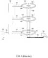
- FIG. 1illustrates a conventional disk drive system 100 .
- Conventional disk drive system 100includes servo tower 102 , servo motor 104 , servo drive apparatus 106 , head arms 108 - 112 , heads 114 - 118 , platters 120 - 124 , spindle shaft 126 , spin motor 128 , spin motor arm 130 , and spin drive apparatus 132 .
- Each of platters 120 - 124stores data on rings called “cylinders,” which extend vertically across platters 120 - 124 .
- Each platteris divided into n cylinders, including cylinder 0 (e.g., 134 - 138 ) and cylinder n (e.g., 140 ).
- Each platteris read and written separately by heads 114 - 118 , each of which accesses data from platters 120 - 124 , respectively.
- Heads 114 - 118electromechanically access the same cylinder simultaneously.
- Servo motor 104moves servo tower 102 , which moves heads 114 - 118 simultaneously across cylinders 134 - 140 .
- the mechanical operation of servo tower 102 , servo motor 104 , and servo drive apparatus 106is controlled by a processor that sends electrical signals to direct forward or backward motion of head arms 108 - 112 and heads 114 - 118 across cylinders 120 - 124 .
- conventional disk drive system 100is limited by latencies incurred by size and the movement of various electromechanical/mechanical components.
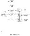
- FIG. 2illustrates a block diagram of a conventional disk drive configuration.
- Conventional implementation 200includes processor 202 , read only memory (ROM) 204 , static random access memory (SRAM) 206 , disk controller 208 , disk interface (I/F) 210 , dynamic random access memory (DRAM) 212 , analog read/write servo power drivers 214 , servo power drivers 216 , and spin motor power drivers 218 .
- SRAMis a type of memory technology that is fast, does not degrade over time, but is volatile (requires a power source to maintain stored data).
- Flash memoryis another type of memory that is non-volatile (i.e., maintains data stored in memory when removed from a power source), but has limited endurance (i.e., gradually loses its stored data in memory over time when operations (e.g., read, write) are “cycled” (i.e., performing a read operation followed by a write operation or vice versa), especially in environments requiring large numbers of accesses.
- Flashalso requires erasing its memory before performing a write operation, which in turn requires a Flash operating system (i.e., a separate application or program) to manage data operations. Additionally, a “shadow” memory (e.g., SRAM) would also be required as a temporary store for data to be erased prior to performing a write operation. When data is erased prior to a write operation, some of the original data may need to be re-written to the Flash memory, which can create erase and write times that are longer than those for a hard disk drive.
- Conventional implementation 200is used with conventional disk drive system 100 described above in connection with FIG. 1 .
- a command signalis sent from a host (not shown) through disk interface 210 to disk controller 208 .
- Processor 202evaluates the command signal and determines the cylinder or set of cylinders where the desired data is located. Once a location has been determined, processor 202 initiates movement of servo tower 102 and positions heads 114 - 118 over the desired cylinder. After mechanically positioning heads 114 - 118 , a data operation is performed to read or write data from/to the selected cylinder. Data is then transferred from the cylinder through disk interface 210 to disk controller 208 , which sends data to DRAM 212 for performing ECC checks and corrections before sending the data over disk interface 210 .
- Conventional systemsalso use operating systems (e.g., Windows®, UNIX®) to manage (e.g., data produced from read, write operations) information.
- an operating systemWhen a file is stored, an operating system records the file name in a directory file.
- the directory fileis typically stored on the first cylinder of a platter and points to a file allocation table (FAT), which contains the location of the desired data file.
- FATsinclude pointers (i.e., cylinder, head sector) to locations for data blocks (i.e., a file may be stored in data blocks in different locations on a platter) of a file.
- FATsare continuously accessed by an operating system, which is typically located on the first cylinders of a platter (e.g., cylinders 134 - 138 ).
- FIG. 1illustrates a conventional disk drive system
- FIG. 2illustrates a block diagram of a conventional disk drive configuration
- FIG. 3illustrates an exemplary system for performing data operations using non-volatile third dimension memory
- FIG. 4illustrates an alternative exemplary system for performing data operations using non-volatile third dimension memory
- FIG. 5illustrates another alternative exemplary system for performing data operations using non-volatile third dimension memory with an integrated controller
- FIG. 6illustrates an exemplary diagram of an integrated controller configured to perform data operations using non-volatile third dimension memory
- FIG. 7illustrates an exemplary controller configured to perform data operations using non-volatile third dimension memory
- FIG. 8illustrates a flow chart of an exemplary process for performing data operations using non-volatile third dimension memory
- FIG. 9is a block diagram illustrating an exemplary computer system suitable for performing data operations using non-volatile third dimension memory.
- the inventioncan be implemented in numerous ways, including as a system, a process, an apparatus, or a computer readable medium such as a computer readable storage medium or a computer network wherein program instructions are sent over optical or electronic communication links.
- a computer readable mediumsuch as a computer readable storage medium or a computer network wherein program instructions are sent over optical or electronic communication links.
- the steps of disclosed processesmay be performed in an arbitrary order, unless otherwise provided in the claims.
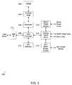
- FIG. 3illustrates an exemplary system for performing data operations using non-volatile third dimension memory.
- system 300includes processor 302 , ROM 304 , SRAM 306 , disk controller 308 , disk interface (I/F) 310 , non-volatile third dimension memory array 312 , analog read/write servo power drivers 314 , servo power drivers 316 , and spin motor power drivers 318 .
- System 300is a memory system configured to perform various data operations with improved (i.e., decreased latencies resulting from mechanical action of disk drive components). In other examples, system 300 may include more or fewer components.
- non-volatile third dimension memory array 312may be used to replace various memory components of system 300 (including DRAM, SRAM, and Flash components) to reduce mechanical action within a disk drive. While primary data blocks for various files may be retrieved using a mechanical disk drive, some components (e.g., directory, FAT) may be accessed using non-volatile third dimension memory array 312 instead.
- non-volatile third dimension memory array 312may be used as a cache or temporary store for data read from or written to a particular memory location (e.g., DRAM).
- non-volatile third dimension memory array 312may be implemented as a DRAM cache in system 300 .
- non-volatile third dimension memory array 312may be implemented and configured differently to achieve fast write operations and high write endurance.
- non-volatile third dimension memory array 312may be implemented internally or externally to disk controller 308 .
- various materials, designs, and fabrication techniquesmay be used and are not limited to the examples described. For example, perovskites and other crystalline materials may be used to implement a memory with desirable characteristics.
- the applicationdescribes a two terminal memory element that changes conductivity when exposed to an appropriate voltage drop across the two terminals.
- the memory elementincludes an electrolytic tunnel barrier and a mixed valence conductive oxide. A voltage drop across the electrolytic tunnel barrier causes an electrical field within the mixed valence conductive oxide that is strong enough to move oxygen ions out of the mixed valence conductive oxides and into the electrolytic tunnel barrier.
- Oxygen depletioncauses the mixed valence conductive oxide to change its valence, which causes a change in conductivity.
- Both the electrolytic tunnel barrier and the mixed valence conductive oxidedo not need to operate in a silicon substrate, and, therefore, can be fabricated above circuitry being used for other purposes (such as selection circuitry).
- a memoryis “third dimension memory” when it is fabricated above other circuitry components, the components usually including a silicon substrate, polysilicon layers and, typically, metallization layers.
- the two-terminal memory elementscan be arranged in a cross point array such that one terminal is electrically coupled with an x-direction line and the other terminal is electrically coupled with a y-direction line.
- a stacked cross point arrayconsists of multiple cross point arrays stacked upon one another, sometimes sharing x-direction and y-direction lines between layers, and sometimes having isolated lines.
- V W2When a second write voltage V W2 is applied across the memory element, (typically by applying 1 ⁇ 2 V W2 to the x-direction line and 1 ⁇ 2-V W2 to the y-direction line) it switches to a high resistive state.
- V W1When a second write voltage V W2 is applied across the memory element, (typically by applying 1 ⁇ 2 V W2 to the x-direction line and 1 ⁇ 2-V W2 to the y-direction line) it switches to a high resistive state.
- V W1typically, memory elements using electrolytic tunnel barriers and mixed valence conductive oxides require V W1 to be opposite in polarity from V W2 .
- non-volatile third dimension memory array 312may be included or embedded with disk controller 308 .
- a read or write commandmay be sent to the first few cylinders of a disk drive.
- the datais instead accessed and taken from non-volatile third dimension memory array 312 and sent to a host (not shown).
- non-volatile third dimension memory array 312stores data (e.g., FAT data, cylinder-head-sector (CHS) values, and the like) that has addresses configured as aliases for addresses assigned to a disk drive.
- datae.g., FAT data, cylinder-head-sector (CHS) values, and the like
- the commandsis interpreted by disk controller 308 to determine a corresponding aliased address in non-volatile third dimension memory array 312 . If the command identifies an address that is included in an aliasing range, a corresponding alias address is used to retrieve data from non-volatile third dimension memory array 312 . Once determined, data stored at the aliased address in non-volatile third dimension memory array 312 is retrieved and sent to the host. The host may use this data to perform other data operations.
- processor 302fetches data from non-volatile third dimension memory array 312 (which is mapped to the FAT and provides aliases identifying locations in non-volatile third dimension memory array 312 ), providing the location of the destination file. This eliminates the need, as in conventional memory systems, to move and settle mechanical servo components over the first few cylinders of a platter where FAT is stored.
- non-volatile third dimension memory array 312By using non-volatile third dimension memory array 312 to replicate FAT data, the additional mechanical action (i.e., movement), access times, rotational latency, head settling delays, disk drive size limitations, the number of “seeks” or data lookups from the FAT, and power requirements are reduced.
- non-volatile third dimension memory array 312may be mapped to an associated disk. Mapping enables non-volatile third dimension memory array 312 to duplicate the image of the first few cylinders of a platter.
- processor 302retrieves data from a disk drive, which is mapped to non-volatile third dimension memory array 312 using cylinder, head, and sector parameters provided in a read or write command.
- Processor 302translates addresses into memory addresses and sequentially fetches the requested data blocks. If a directory or FAT is written to a memory address, the data to be written may be retrieved from a holding buffer within controller 308 . The directory or FAT data may then be sequentially written to non-volatile third dimension memory array 312 using a direct memory access (DMA) sequence orchestrated by the controller. DMA is described below in connection with FIG. 7 .
- DMAdirect memory access
- Non-volatile third dimension memory array 312may be used in various implementations.
- non-volatile third dimension memory array 312may be used to replace DRAM typically used to store the data and command packets as shown in FIG. 2 .
- DRAM interfaceBy using a DRAM interface (not shown), non-volatile third dimension memory array 312 may be used to replace DRAM, as shown in this example.
- non-volatile third dimension memory arraymay be used to replace Flash/ROM 304 used with processor 302 .
- FIG. 4illustrates an alternative exemplary system for performing data operations using non-volatile third dimension memory.
- system 400includes processor 402 , non-volatile third dimension memory array 404 , disk controller 406 , disk interface (I/F) 408 , DRAM 410 , analog read/write servo power drivers 412 , servo power drivers 414 , and spin motor power drivers 416 .
- System 400is storage or memory system that may be used as a replacement, complement, or supplement to a disk drive (e.g., hard disk drive, RAID, and the like). In other examples, system 400 may include more or fewer components.
- non-volatile third dimension memory array 404may be used to replace a Flash or ROM component to system 400 .
- Non-volatile third dimension memory array 404may be used to replace Flash or ROM technologies by combining program memory with cylinder cache tables (e.g., FAT).
- processor 402detects an access request (i.e., command signal) for a cylinder corresponding to FAT, data is accessed, read, or written from disk controller 406 .
- Flash or ROM memorymay be replaced by mapping data stored on non-volatile third dimension memory array 404 to an address or location on a cylinder. Instead of retrieving data from Flash or ROM, non-volatile third dimension memory array 404 provides the requested data in response to the access request without requiring additional mechanical action.
- non-volatile third dimension memory array 404may be used to replace other components of a storage or memory system.
- FIG. 5illustrates another alternative exemplary system for performing data operations using non-volatile third dimension memory with an integrated controller.
- system 500includes integrated controller 502 , disk interface (I/F) 504 , analog read/write servo power drivers 506 , servo power drivers 508 , and spin motor power drivers 510 .
- integrated controller 502combines several functions, including those provided by a disk controller, processor, and, in some examples, various memory devices, systems, or stores (e.g., SRAM, DRAM, Flash, ROM, and the like).
- a non-volatile third dimension memory arrayis included (i.e., integrated, embedded) with integrated controller 502 , which also includes a processor and disk controller.
- Flash/ROM and SRAMare external to integrated controller 502 . In other examples, Flash/ROM and SRAM are included with integrated controller 502 . By combining several functions within integrated controller 502 , die sizes, mechanical action, power requirements, and other limiting factors in conventional disk drives may be reduced. Additionally, by combining multiple functions into integrated controller 502 may be vertically configured, as described in greater detail below in connection with FIG. 6 .
- FIG. 6illustrates an exemplary diagram of an integrated controller configured to perform data operations using non-volatile third dimension memory.
- an integrated controllere.g., integrated controller 502 of FIG. 5
- an integrated controllermay be implemented by using a vertical chip configuration.
- “Chip”may refer to a semiconductor system, integrated circuit, application-specific integrated circuit, or other circuit design embedded on a wafer or substrate.
- chip 600includes processor 602 and disk controller 604 formed on a substrate (not shown) or another supportive layer. Layered on top of processor 602 and disk controller 604 are data/DRAM replacement memory 606 , Flash/SRAM replacement memory 608 , and cylinder cache (e.g., Flash/ROM) 610 .
- data/DRAM replacement memory 606 , Flash/SRAM replacement memory 608 , and cylinder cache (e.g., Flash/ROM) 610are layers that may be replaced using a non-volatile third dimension memory array such as that described above in connection with FIG. 3 .
- the die size of chip 600may be reduced by vertically configuring various memory systems to reduce the overall die size.
- the die size of chip 600is determined by the die size of an included disk controller included, which may allow large blocks or planes of memory to be vertically disposed (e.g., on top of, underneath, stacked) relative to the disk controller.
- a non-volatile third dimension memory planemay be used to replace Flash/ROM memory.
- a non-volatile third dimension memory planemay replace SRAM memory.
- Another non-volatile third dimension memory planemay be used to replace DRAM used for data passing and the cylinder cache.
- individual non-volatile third dimension memory planesmay be used to implement data passing and cylinder caching functions independently.
- non-volatile third dimension memory planesmay be shared. For example, SRAM and Flash memory may be replaced by a single memory plane, a set of sub-planes, or divided blocks on a plane.
- FIG. 7illustrates an exemplary controller configured to perform data operations using non-volatile third dimension memory.
- Disk controller 700may be used as a component in a system configured to perform data operations using non-volatile third dimension memory, such as those described above in connection with FIGS. 3 , 4 , and 5 .
- Disk controller 700may be fabricated using memory systems that enable data to be read or written from/to various memory locations.
- disk controller 700includes processor 702 , SRAM memory 703 , read only memory (ROM) 704 , random access memory (RAM) 706 , memory controller 708 , host interface (I/F) block 710 , direct memory access (DMA) block 712 , buffer memories 714 - 716 , error correction code (which may also be referred to as error checking and correction or ECC) 718 , defect management block 720 , disk interface 722 , and interface (I/F) state machine (SM) 724 .
- buffer memories 714 - 716may be small buffers used for speed matching between host I/F block 710 and disk I/F 722 , which transfers driving and receiving signals between controller 700 and a disk in a storage system (not shown).
- Buffer memories 714 - 716may be implemented as a first-in, first-out (FIFO)-type buffer. In other examples, buffer memories 714 - 716 may be implemented differently. Memory in disk controller 700 may be implemented as RAM, ROM, dynamic random access memory (DRAM), static/dynamic random access memory (SDRAM), or other technologies. Buffer memories 714 - 716 may also be implemented to temporarily store and access data while disk controller 700 is operating (i.e., receiving power) enabling faster data processing. Other components are described, including logic for controlling operations that access memory locations throughout disk controller 700 .
- disk controller 700Components may be referred to as “blocks” or “modules.”
- the various blocks included in disk controller 700may be used to implement functionality for a storage system that interfaces with various internal memory systems (hereafter “memory”) and external devices that are either requesting or storing data in disk controller 700 .
- External devicesmay include other software or hardware that, through I/F Drv/Rec 722 , interfaces with disk controller 700 to retrieve or store data.
- more or fewer blocksmay be included in disk controller 700 . Further, different blocks may be used to implement various types of functionality beyond that described above.
- processor 702provides logic configured to provide controller functions.
- Software code written in languages such as Cmay provide instruction sets on how disk controller 700 (i.e., processor 702 and memory controller 708 ) processes requests to either retrieve or store data from various memory locations in system 702 .
- Other functions performed by processor 702may include initializing controller logic when power is applied (i.e., “on” voltage is applied), performing diagnostic checks, interpreting commands for memory functions, memory management, ECC-related functions, and others.
- Processor 702also interprets commands from host I/F block 710 to establish data flow control using DMA block 712 .
- Host I/F block 710may be used to implement complex functionality that enables disk controller 700 to integrate with other systems, for example, in a computer.
- host I/F block 710Some functions that may be performed by host I/F block 710 include encoding/decoding (e.g., 8-bit/10-bit), scrambling (to reduce electromagnetic interference (EMI)), parity/cyclic redundancy check (CRC)/ECC checking, disparity generation and checking, interface state machine functions, data buffer (e.g., first-in, first-out (FIFO)) buffer, alignment and primitive check and generation (e.g., checks performed on serial interfaces), and others. Some of these functions may also be implemented using other blocks in disk controller 700 .
- encoding/decodinge.g., 8-bit/10-bit
- scramblingto reduce electromagnetic interference (EMI)
- CRCparity/cyclic redundancy check
- CRCparity/cyclic redundancy check
- disparity generation and checkinginterface state machine functions
- data buffere.g., first-in, first-out (FIFO) buffer
- alignment and primitive check and generatione.g., checks performed on serial interfaces
- disk controller 700may be implemented as a memory card, including memory storage and controller logic.
- a memory cardmay be connected to host interface block 710 using an interface connector (not shown).
- a chip using disk controller 700may be configured to receive electrical signals from external devices through an interface connector. The electrical signals are interpreted and acted upon depending upon an interface standard (e.g., IEEE) used for command and data passing. Electrical signals may be sent and received to pass data to and from memory 706 via host I/F block 710 and memory controller 708 .
- Host I/F block 710sends commands and data to memory 706 via DMA 112 and memory controller 708 .
- memory controller 708may be implemented as a DRAM controller, which may be used to access, retrieve, and store data in memory 706 while power is being supplied. Memory controller 708 also determines addresses for data stored in memory 706 . Addresses may be referenced, for example, based on a row and column reference for a particular cell in a given memory array. By selectively applying voltages to terminals connected to row and column leads, the resistive states of various materials (e.g., ferroelectric, perovskite, and others) used in memory cells may be changed.
- various materialse.g., ferroelectric, perovskite, and others
- the resistive states of memory cellsmay be changed to store data bits (e.g., whether a cell's resistive state indicates a “0” or “1” or, in the case of a four level multi-level memory cell, whether a cell's resistive state indicates a “00” “01” “10” or “11”).
- blocks within disk controller 700may be vertically configured as third dimension memory.
- memory 704 or memory 706may be vertically configured relative to the other blocks of disk controller 700 .
- additional memory controllers or memory locationsmay be layered in a vertical configuration.
- Disk controller 700may use multiple memory controllers to enable faster data retrieval and storage from various memory locations.
- DRAM technologymay be used to implement memory 706 and memory controller 708 .
- DRAMuses a “pulse” or refresh voltage in order to retain data in memory while power is on.
- Memory controller 708may be implemented using logic that processes data stored in and retrieved from memory 706 .
- multiple DRAM-based memory controllersmay be used in order to increase processing times.
- multiple memory layers of third dimension memorymay be used to increase storage capacity.
- Third dimension memoriesmay include vertically-stacked, cross-point, two or three-terminal memory arrays fabricated and configured for high-density and fast operation (e.g., read, write) performance.
- Disk controller 700may also include logic that determines how data is shared with external devices.
- I/F SM 724may be configured to send or receive data from an external device indicated by addresses in electrical signals.
- a “handshake”may be performed with the indicated external device through a I/F Dev/Rec module 722 , which acts as a memory interface bus to establish a connection.
- I/F Dev/Rec module 722works in conjunction with I/F SM 724 , which performs handshaking and data flow handling to external devices using data in memory 704 or 706 controlled by disk controller 700 .
- I/F SM 724may also include other functionality to support interfaces between disk controller 700 and external devices. Devices may also include other processes, logic, circuits, components, or functionality included in an IC.
- Memory 704 or 706may be implemented as third dimension memories to reduce die size. Multiple memory layers may be vertically stacked in order to increase storage capacity of chips without increasing die sizes. Memory 704 and/or 706 and memory controller 708 may be configured to occupy the same die area, but are vertically stacked in layers or “planes.” A vertical configuration thereby reduces overall die size, reduces manufacturing and test costs, and increases capacity. This configuration allows multiple planes of memory to be placed on top of or below memory controller 708 .
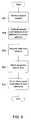
- FIG. 8illustrates a flow chart of an exemplary process for performing data operations using non-volatile third dimension memory.
- a processore.g., processor 302 or 402 and integrated controller 502
- an access requestis received, which may include a drive address (i.e., an address on a disk drive for a specific data value or set of values) ( 802 ).
- An access requestmay be a command sent from a host over a disk interface to a processor in order to perform a data operation (e.g., read or write data from a particular file stored in memory).
- the access requestis interpreted and a drive address is translated into a memory address ( 804 ).
- data indicating the address, sequence of data blocks, cylinder, sectors, and other parameters of the requested datais requested and provided from the non-volatile third dimension memory array, instead of from the first few cylinders of a platter ( 806 ). This enables the reduction of mechanical action (i.e., movement), access times, rotational latency, head settling delays, disk drive size limitations, the number of “seeks” or data lookups from the FAT, and power requirements.
- the datais sent to the host ( 808 ). Subsequently, the host signals or commands the performance of a desired data operation and the necessary signals are sent to the various drivers (e.g., analog read/write servo power drivers, servo power drivers, and spin motor power drivers, and the like).
- the processorthen enters an idle state and waits for the next command ( 810 ).
- the above-described processmay be varied in such ways that more or fewer sub-processes may be implemented. Further, the process is not limited to the implementation example shown. In some examples, the process shown may be implemented as a set of instructions executed in hardware, software, circuitry, or a combination thereof. An exemplary processor configured to execute the described process is described in connection with FIG. 9 .
- FIG. 9is a block diagram illustrating an exemplary computer system suitable for performing data operations using non-volatile third dimension memory.
- computer system 900may be used to implement computer programs, applications, methods, or other software to perform the above-described techniques for fabricating storage systems such as those described above.
- Computer system 900includes a bus 902 or other communication mechanism for communicating information, which interconnects subsystems and devices, such as processor 904 , system memory 906 (e.g., RAM), storage device 908 (e.g., ROM), disk drive 910 (e.g., magnetic or optical), communication interface 912 (e.g., modem or Ethernet card), display 914 (e.g., CRT or LCD), input device 916 (e.g., keyboard), and cursor control 918 (e.g., mouse or trackball).
- processor 904system memory 906 (e.g., RAM), storage device 908 (e.g., ROM), disk drive 910 (e.g., magnetic or optical), communication interface 912 (e.g., modem or Ethernet card), display 914 (e.g., CRT or LCD), input device 916 (e.g., keyboard), and cursor control 918 (e.g., mouse or trackball).
- system memory 906e.g., RAM
- computer system 900performs specific operations by processor 904 executing one or more sequences of one or more instructions stored in system memory 906 .
- Such instructionsmay be read into system memory 906 from another computer readable medium, such as static storage device 908 or disk drive 910 .
- static storage device 908 or disk drive 910may be used in place of or in combination with software instructions to implement the invention.
- Non-volatile mediaincludes, for example, optical or magnetic disks, such as disk drive 910 .
- Transmission mediaincludes coaxial cables, copper wire, and fiber optics, including wires that comprise bus 902 . Transmission media can also take the form of acoustic or light waves, such as those generated during radio wave and infrared data communications.
- Computer readable mediaincludes, for example, floppy disk, flexible disk, hard disk, magnetic tape, any other magnetic medium, CD-ROM, any other optical medium, punch cards, paper tape, any other physical medium with patterns of holes, RAM, PROM, EPROM, FLASH-EPROM, any other memory chip or cartridge, carrier wave, or any other medium from which a computer can read.
- Computer system 900may transmit and receive messages, data, and instructions, including program, i.e., application code, through communication link 920 and communication interface 912 .
- Received program codemay be executed by processor 904 as it is received, and/or stored in disk drive 910 , or other non-volatile storage for later execution.
Landscapes
- Engineering & Computer Science (AREA)
- Theoretical Computer Science (AREA)
- Physics & Mathematics (AREA)
- General Engineering & Computer Science (AREA)
- General Physics & Mathematics (AREA)
- Human Computer Interaction (AREA)
- Signal Processing For Digital Recording And Reproducing (AREA)
- Techniques For Improving Reliability Of Storages (AREA)
Abstract
Description
Claims (28)
Priority Applications (4)
| Application Number | Priority Date | Filing Date | Title |
|---|---|---|---|
| US11/478,163US7747817B2 (en) | 2006-06-28 | 2006-06-28 | Performing data operations using non-volatile third dimension memory |
| US12/803,542US7870333B2 (en) | 2006-06-28 | 2010-06-29 | Performing data operations using non-volatile third dimension memory |
| US12/930,628US8065478B2 (en) | 2006-06-28 | 2011-01-11 | Performing data operations using non-volatile third dimension memory |
| US13/303,009US20120063191A1 (en) | 2006-06-28 | 2011-11-22 | Performing Data Operations Using Non Volatile Third Dimension Memory |
Applications Claiming Priority (1)
| Application Number | Priority Date | Filing Date | Title |
|---|---|---|---|
| US11/478,163US7747817B2 (en) | 2006-06-28 | 2006-06-28 | Performing data operations using non-volatile third dimension memory |
Related Child Applications (1)
| Application Number | Title | Priority Date | Filing Date |
|---|---|---|---|
| US12/803,542ContinuationUS7870333B2 (en) | 2006-06-28 | 2010-06-29 | Performing data operations using non-volatile third dimension memory |
Publications (2)
| Publication Number | Publication Date |
|---|---|
| US20080005459A1 US20080005459A1 (en) | 2008-01-03 |
| US7747817B2true US7747817B2 (en) | 2010-06-29 |
Family
ID=38878213
Family Applications (4)
| Application Number | Title | Priority Date | Filing Date |
|---|---|---|---|
| US11/478,163Expired - Fee RelatedUS7747817B2 (en) | 2006-06-28 | 2006-06-28 | Performing data operations using non-volatile third dimension memory |
| US12/803,542Expired - Fee RelatedUS7870333B2 (en) | 2006-06-28 | 2010-06-29 | Performing data operations using non-volatile third dimension memory |
| US12/930,628Expired - Fee RelatedUS8065478B2 (en) | 2006-06-28 | 2011-01-11 | Performing data operations using non-volatile third dimension memory |
| US13/303,009AbandonedUS20120063191A1 (en) | 2006-06-28 | 2011-11-22 | Performing Data Operations Using Non Volatile Third Dimension Memory |
Family Applications After (3)
| Application Number | Title | Priority Date | Filing Date |
|---|---|---|---|
| US12/803,542Expired - Fee RelatedUS7870333B2 (en) | 2006-06-28 | 2010-06-29 | Performing data operations using non-volatile third dimension memory |
| US12/930,628Expired - Fee RelatedUS8065478B2 (en) | 2006-06-28 | 2011-01-11 | Performing data operations using non-volatile third dimension memory |
| US13/303,009AbandonedUS20120063191A1 (en) | 2006-06-28 | 2011-11-22 | Performing Data Operations Using Non Volatile Third Dimension Memory |
Country Status (1)
| Country | Link |
|---|---|
| US (4) | US7747817B2 (en) |
Cited By (5)
| Publication number | Priority date | Publication date | Assignee | Title |
|---|---|---|---|---|
| US20100195363A1 (en)* | 2009-01-30 | 2010-08-05 | Unity Semiconductor Corporation | Multiple layers of memory implemented as different memory technology |
| US20110107001A1 (en)* | 2006-06-28 | 2011-05-05 | Unity Semiconductor Corporation | Performing data operations using non-volatile third dimension memory |
| US8141021B2 (en)* | 2004-02-06 | 2012-03-20 | Unity Semiconductor Corporation | Combined memories in integrated circuits |
| US10371761B2 (en)* | 2013-12-31 | 2019-08-06 | MultiDimension Technology Co., Ltd. | Low profile magnetoresistive imaging sensor array |
| US12090803B2 (en) | 2020-06-18 | 2024-09-17 | Bazooka-Farmstar, LLC | Amphibious vehicle |
Families Citing this family (48)
| Publication number | Priority date | Publication date | Assignee | Title |
|---|---|---|---|---|
| US20130082232A1 (en) | 2011-09-30 | 2013-04-04 | Unity Semiconductor Corporation | Multi Layered Conductive Metal Oxide Structures And Methods For Facilitating Enhanced Performance Characteristics Of Two Terminal Memory Cells |
| US8111572B2 (en)* | 2007-12-12 | 2012-02-07 | Unity Semiconductor Corporation | Disturb control circuits and methods to control memory disturbs among multiple layers of memory |
| US9058300B2 (en)* | 2005-03-30 | 2015-06-16 | Unity Semiconductor Corporation | Integrated circuits and methods to control access to multiple layers of memory |
| US7889571B2 (en) | 2008-01-09 | 2011-02-15 | Unity Semiconductor Corporation | Buffering systems methods for accessing multiple layers of memory in integrated circuits |
| US7649788B2 (en)* | 2006-01-30 | 2010-01-19 | Unity Semiconductor Corporation | Buffering systems for accessing multiple layers of memory in integrated circuits |
| DE102007001537A1 (en)* | 2007-01-10 | 2008-07-17 | Siemens Audiologische Technik Gmbh | Influenzladevorrichtung and corresponding method |
| US8533847B2 (en)* | 2007-05-24 | 2013-09-10 | Sandisk Il Ltd. | Apparatus and method for screening new data without impacting download speed |
| US7715250B2 (en)* | 2007-08-16 | 2010-05-11 | Unity Semiconductor Corporation | Circuitry and method for indicating a memory |
| US8165621B2 (en)* | 2007-10-10 | 2012-04-24 | Unity Semiconductor Corporation | Memory emulation in a cellular telephone |
| US7593284B2 (en)* | 2007-10-17 | 2009-09-22 | Unity Semiconductor Corporation | Memory emulation using resistivity-sensitive memory |
| US7796451B2 (en)* | 2007-12-10 | 2010-09-14 | Unity Semiconductor Corporation | Integrated circuits and methods to compensate for defective memory in multiple layers of memory |
| US7822913B2 (en)* | 2007-12-20 | 2010-10-26 | Unity Semiconductor Corporation | Emulation of a NAND memory system |
| US7751221B2 (en)* | 2007-12-21 | 2010-07-06 | Unity Semiconductor Corporation | Media player with non-volatile memory |
| US7877541B2 (en)* | 2007-12-22 | 2011-01-25 | Unity Semiconductor Corporation | Method and system for accessing non-volatile memory |
| US20090164203A1 (en)* | 2007-12-23 | 2009-06-25 | Unity Semiconductor Corporation | Non-volatile memory compiler |
| US20090164744A1 (en)* | 2007-12-24 | 2009-06-25 | Unity Semiconductor Corporation | Memory access protection |
| US20090171650A1 (en)* | 2007-12-27 | 2009-07-02 | Unity Semiconductor Corporation | Non-Volatile memories in interactive entertainment systems |
| US20090172350A1 (en)* | 2007-12-28 | 2009-07-02 | Unity Semiconductor Corporation | Non-volatile processor register |
| US7652502B2 (en) | 2007-12-29 | 2010-01-26 | Unity Semiconductor Corporation | Field programmable gate arrays using resistivity sensitive memories |
| US7834660B2 (en)* | 2007-12-30 | 2010-11-16 | Unity Semiconductor Corporation | State machines using resistivity-sensitive memories |
| US20090167496A1 (en)* | 2007-12-31 | 2009-07-02 | Unity Semiconductor Corporation | Radio frequency identification transponder memory |
| US7652501B2 (en) | 2008-01-07 | 2010-01-26 | Unity Semiconductor Corporation | Programmable logic device structure using third dimensional memory |
| US7818523B2 (en)* | 2008-01-10 | 2010-10-19 | Unity Semiconductor Corporation | Securing data in memory device |
| US7715244B2 (en)* | 2008-02-05 | 2010-05-11 | Unity Semiconductor Corporation | Non-volatile register having a memory element and register logic vertically configured on a substrate |
| US7990762B2 (en) | 2008-02-06 | 2011-08-02 | Unity Semiconductor Corporation | Integrated circuits to control access to multiple layers of memory |
| US20090193980A1 (en)* | 2008-02-06 | 2009-08-06 | Man-Yan Chan | Popcorn cooking and dispensing appliance |
| US9548108B2 (en)* | 2008-06-18 | 2017-01-17 | Super Talent Technology, Corp. | Virtual memory device (VMD) application/driver for enhanced flash endurance |
| US9547589B2 (en)* | 2008-06-18 | 2017-01-17 | Super Talent Technology, Corp. | Endurance translation layer (ETL) and diversion of temp files for reduced flash wear of a super-endurance solid-state drive |
| US8959280B2 (en)* | 2008-06-18 | 2015-02-17 | Super Talent Technology, Corp. | Super-endurance solid-state drive with endurance translation layer (ETL) and diversion of temp files for reduced flash wear |
| US8281074B2 (en) | 2008-10-07 | 2012-10-02 | Micron Technology, Inc. | Interface device for memory in a stack, storage devices and a processor |
| US9015209B2 (en)* | 2008-12-16 | 2015-04-21 | Sandisk Il Ltd. | Download management of discardable files |
| US20100153474A1 (en)* | 2008-12-16 | 2010-06-17 | Sandisk Il Ltd. | Discardable files |
| US9020993B2 (en) | 2008-12-16 | 2015-04-28 | Sandisk Il Ltd. | Download management of discardable files |
| US9104686B2 (en) | 2008-12-16 | 2015-08-11 | Sandisk Technologies Inc. | System and method for host management of discardable objects |
| US8375192B2 (en)* | 2008-12-16 | 2013-02-12 | Sandisk Il Ltd. | Discardable files |
| US8849856B2 (en) | 2008-12-16 | 2014-09-30 | Sandisk Il Ltd. | Discardable files |
| US8205060B2 (en)* | 2008-12-16 | 2012-06-19 | Sandisk Il Ltd. | Discardable files |
| US20100185816A1 (en)* | 2009-01-21 | 2010-07-22 | Sauber William F | Multiple Cache Line Size |
| US20100235329A1 (en)* | 2009-03-10 | 2010-09-16 | Sandisk Il Ltd. | System and method of embedding second content in first content |
| US20100333155A1 (en)* | 2009-06-30 | 2010-12-30 | Philip David Royall | Selectively using local non-volatile storage in conjunction with transmission of content |
| US8463802B2 (en) | 2010-08-19 | 2013-06-11 | Sandisk Il Ltd. | Card-based management of discardable files |
| US8549229B2 (en) | 2010-08-19 | 2013-10-01 | Sandisk Il Ltd. | Systems and methods for managing an upload of files in a shared cache storage system |
| US8788849B2 (en) | 2011-02-28 | 2014-07-22 | Sandisk Technologies Inc. | Method and apparatus for protecting cached streams |
| US10127150B2 (en) | 2012-11-09 | 2018-11-13 | Sandisk Technologies Llc | Key value addressed storage drive using NAND flash based content addressable memory |
| US9075424B2 (en) | 2013-03-06 | 2015-07-07 | Sandisk Technologies Inc. | Compensation scheme to improve the stability of the operational amplifiers |
| US9678689B2 (en)* | 2013-05-29 | 2017-06-13 | Microsoft Technology Licensing, Llc | Storage systems and aliased memory |
| US11074151B2 (en) | 2018-03-30 | 2021-07-27 | Intel Corporation | Processor having embedded non-volatile random access memory to support processor monitoring software |
| US10691466B2 (en)* | 2018-04-02 | 2020-06-23 | Intel Corporation | Booting a computing system using embedded non-volatile memory |
Citations (24)
| Publication number | Priority date | Publication date | Assignee | Title |
|---|---|---|---|---|
| US3886577A (en) | 1973-09-12 | 1975-05-27 | Energy Conversion Devices Inc | Filament-type memory semiconductor device and method of making the same |
| US5296716A (en) | 1991-01-18 | 1994-03-22 | Energy Conversion Devices, Inc. | Electrically erasable, directly overwritable, multibit single cell memory elements and arrays fabricated therefrom |
| US5526507A (en)* | 1992-01-06 | 1996-06-11 | Hill; Andrew J. W. | Computer memory array control for accessing different memory banks simullaneously |
| US6034882A (en)* | 1998-11-16 | 2000-03-07 | Matrix Semiconductor, Inc. | Vertically stacked field programmable nonvolatile memory and method of fabrication |
| US6204139B1 (en) | 1998-08-25 | 2001-03-20 | University Of Houston | Method for switching the properties of perovskite materials used in thin film resistors |
| US6473332B1 (en) | 2001-04-04 | 2002-10-29 | The University Of Houston System | Electrically variable multi-state resistance computing |
| US6487106B1 (en) | 1999-01-12 | 2002-11-26 | Arizona Board Of Regents | Programmable microelectronic devices and method of forming and programming same |
| US6531371B2 (en) | 2001-06-28 | 2003-03-11 | Sharp Laboratories Of America, Inc. | Electrically programmable resistance cross point memory |
| US6545891B1 (en)* | 2000-08-14 | 2003-04-08 | Matrix Semiconductor, Inc. | Modular memory device |
| US20030132456A1 (en) | 1998-09-08 | 2003-07-17 | Yoichi Miyai | Method of forming cross point type DRAM cell |
| US6657888B1 (en) | 2001-05-11 | 2003-12-02 | Board Of Regents Of The University Of Nebraska | Application of high spin polarization materials in two terminal non-volatile bistable memory devices |
| US6731528B2 (en) | 2002-05-03 | 2004-05-04 | Micron Technology, Inc. | Dual write cycle programmable conductor memory system and method of operation |
| US6753561B1 (en) | 2002-08-02 | 2004-06-22 | Unity Semiconductor Corporation | Cross point memory array using multiple thin films |
| US20040141369A1 (en) | 2003-01-20 | 2004-07-22 | Oki Electric Industry Co., Ltd. | Semiconductor integrated circuit |
| US6807088B2 (en) | 2003-02-17 | 2004-10-19 | Kabushiki Kaisha Toshiba | Magnetic random access memory and reading method thereof |
| US6825489B2 (en) | 2001-04-06 | 2004-11-30 | Axon Technologies Corporation | Microelectronic device, structure, and system, including a memory structure having a variable programmable property and method of forming the same |
| US6836421B2 (en) | 2002-08-02 | 2004-12-28 | Unity Semiconductor Corporation | Line drivers that fit within a specified line pitch |
| US6856536B2 (en) | 2002-08-02 | 2005-02-15 | Unity Semiconductor Corporation | Non-volatile memory with a single transistor and resistive memory element |
| US20050135148A1 (en) | 2003-12-22 | 2005-06-23 | Unity Semiconductor Corporation | Conductive memory array having page mode and burst mode read capability |
| US20050151156A1 (en) | 2004-01-13 | 2005-07-14 | Wu Naijuan | Switchable resistive perovskite microelectronic device with multi-layer thin film structure |
| US7002197B2 (en) | 2004-01-23 | 2006-02-21 | Hewlett-Packard Development Company, L.P. | Cross point resistive memory array |
| US20060050598A1 (en) | 2004-09-03 | 2006-03-09 | Darrell Rinerson | Memory using variable tunnel barrier widths |
| US20060164882A1 (en) | 2004-12-23 | 2006-07-27 | Robert Norman | Storage controller using vertical memory |
| US20060171200A1 (en)* | 2004-02-06 | 2006-08-03 | Unity Semiconductor Corporation | Memory using mixed valence conductive oxides |
Family Cites Families (1)
| Publication number | Priority date | Publication date | Assignee | Title |
|---|---|---|---|---|
| US7747817B2 (en)* | 2006-06-28 | 2010-06-29 | Unity Semiconductor Corporation | Performing data operations using non-volatile third dimension memory |
- 2006
- 2006-06-28USUS11/478,163patent/US7747817B2/ennot_activeExpired - Fee Related
- 2010
- 2010-06-29USUS12/803,542patent/US7870333B2/ennot_activeExpired - Fee Related
- 2011
- 2011-01-11USUS12/930,628patent/US8065478B2/ennot_activeExpired - Fee Related
- 2011-11-22USUS13/303,009patent/US20120063191A1/ennot_activeAbandoned
Patent Citations (24)
| Publication number | Priority date | Publication date | Assignee | Title |
|---|---|---|---|---|
| US3886577A (en) | 1973-09-12 | 1975-05-27 | Energy Conversion Devices Inc | Filament-type memory semiconductor device and method of making the same |
| US5296716A (en) | 1991-01-18 | 1994-03-22 | Energy Conversion Devices, Inc. | Electrically erasable, directly overwritable, multibit single cell memory elements and arrays fabricated therefrom |
| US5526507A (en)* | 1992-01-06 | 1996-06-11 | Hill; Andrew J. W. | Computer memory array control for accessing different memory banks simullaneously |
| US6204139B1 (en) | 1998-08-25 | 2001-03-20 | University Of Houston | Method for switching the properties of perovskite materials used in thin film resistors |
| US20030132456A1 (en) | 1998-09-08 | 2003-07-17 | Yoichi Miyai | Method of forming cross point type DRAM cell |
| US6034882A (en)* | 1998-11-16 | 2000-03-07 | Matrix Semiconductor, Inc. | Vertically stacked field programmable nonvolatile memory and method of fabrication |
| US6487106B1 (en) | 1999-01-12 | 2002-11-26 | Arizona Board Of Regents | Programmable microelectronic devices and method of forming and programming same |
| US6545891B1 (en)* | 2000-08-14 | 2003-04-08 | Matrix Semiconductor, Inc. | Modular memory device |
| US6473332B1 (en) | 2001-04-04 | 2002-10-29 | The University Of Houston System | Electrically variable multi-state resistance computing |
| US6825489B2 (en) | 2001-04-06 | 2004-11-30 | Axon Technologies Corporation | Microelectronic device, structure, and system, including a memory structure having a variable programmable property and method of forming the same |
| US6657888B1 (en) | 2001-05-11 | 2003-12-02 | Board Of Regents Of The University Of Nebraska | Application of high spin polarization materials in two terminal non-volatile bistable memory devices |
| US6531371B2 (en) | 2001-06-28 | 2003-03-11 | Sharp Laboratories Of America, Inc. | Electrically programmable resistance cross point memory |
| US6731528B2 (en) | 2002-05-03 | 2004-05-04 | Micron Technology, Inc. | Dual write cycle programmable conductor memory system and method of operation |
| US6753561B1 (en) | 2002-08-02 | 2004-06-22 | Unity Semiconductor Corporation | Cross point memory array using multiple thin films |
| US6836421B2 (en) | 2002-08-02 | 2004-12-28 | Unity Semiconductor Corporation | Line drivers that fit within a specified line pitch |
| US6856536B2 (en) | 2002-08-02 | 2005-02-15 | Unity Semiconductor Corporation | Non-volatile memory with a single transistor and resistive memory element |
| US20040141369A1 (en) | 2003-01-20 | 2004-07-22 | Oki Electric Industry Co., Ltd. | Semiconductor integrated circuit |
| US6807088B2 (en) | 2003-02-17 | 2004-10-19 | Kabushiki Kaisha Toshiba | Magnetic random access memory and reading method thereof |
| US20050135148A1 (en) | 2003-12-22 | 2005-06-23 | Unity Semiconductor Corporation | Conductive memory array having page mode and burst mode read capability |
| US20050151156A1 (en) | 2004-01-13 | 2005-07-14 | Wu Naijuan | Switchable resistive perovskite microelectronic device with multi-layer thin film structure |
| US7002197B2 (en) | 2004-01-23 | 2006-02-21 | Hewlett-Packard Development Company, L.P. | Cross point resistive memory array |
| US20060171200A1 (en)* | 2004-02-06 | 2006-08-03 | Unity Semiconductor Corporation | Memory using mixed valence conductive oxides |
| US20060050598A1 (en) | 2004-09-03 | 2006-03-09 | Darrell Rinerson | Memory using variable tunnel barrier widths |
| US20060164882A1 (en) | 2004-12-23 | 2006-07-27 | Robert Norman | Storage controller using vertical memory |
Non-Patent Citations (20)
| Title |
|---|
| A. Beck, J. Bednorz, A. Bietsch, Ch. Gerber, C. Rossel, D. Widmer, "Reproducible switching effect in thin oxide films for memory applications," Applied Physics Letters, vol. 77, No. 1, Jul. 3, 2000, pp. 139-141. |
| A. J. Millis, "Cooperative Jahn-Teller effect and electron-phonon coupling in La1-xAxMnO3," Phys. Rev. B 53, 8434-8441 (1996). |
| A. Reller, J. M. Thomas, D. A. Jefferson, M. K. Uppal, "Superstructures Formed by the Ordering of Vacancies in a Selective Oxidation Catalyst: Grossly Defective CaMnO3," Proceedings of the Royal Society of London, vol. 394, No. 1807 Aug. 1984, pp. 223-241. |
| A. Sawa, et al, "Hysteretic current-volyage characteristics and resisitance switching at a rectifying Ti/Pr0.7Ca0.3MnO3 interface" Applied Physics Letters, vol. 85, No. 18, Nov. 1, 2004, pp. 4073-4075. |
| A.Baikalov, et al, "Field -driven hysteretic and reversible resistive switch at the Ag-Pr0.7Ca0.3MnO3 interface" Applied Physics Letters, vol. 83, No. 5, Aug. 4, 2003, pp. 957-959. |
| B. C. H. Steele, A. Heinzel, "Materials for Fuel-Cell Technologies," Nature 414, Nov. 2001, pp. 345-352. |
| C. Rossel, G.I. Meijer, D. Brémaud, D. Widmer, "Electrical current distribution across a metal-insulator-metal structure during bistable switching," Journal of Applied Physics, vol. 90, No. 6, Sep. 15, 2001, pp. 2892-2898. |
| David Oxley, "Memory Effects in Oxide Films" in Oxides and Oxide Films, vol. 6, pp. 251-325 (Chapter 4) (Ashok. K. Vijh ed., Marcel Drekker) (1981). |
| J. Mizusaki J, Y. Yonemura, H. Kamata, K. Ohyama, N. Mori, H. Takai, H. Tagawa, M. Dokiya, K. Naraya, T. Sasamoto, H. Inaba, T. Hashimoto, "Electronic conductivity, Seebeck coefficient, defect and electronic structure of nonstoichimetric La1-xSrxMnO3," Solid State Ionics 132, 167 (2000). |
| J. R. Stetter, W. R. Penrose, S. Yao, "Sensors, Chemical Sensors, Electrochemical Sensors, and ECS," Journal of The Electrochemical Society, 150 (2), S11-S16 (2003). |
| J.G. Simmons and R.R. Verderber, "New Conduction and Reversible Memory Phenomena in Thin Insulating Films," Proc. Roy. Soc. A., 301 (1967), pp. 77-102. |
| Liu et al., "A New Concept for Non-Volatile Memory: The Electric-Pulse Induced Resistive Change Effect in Colossal Magnetoresistive Thin Films," Non-Volatile Memory Technology Symposium, Nov. 7, 2001, pp. 1-7. |
| Liu et al., "Electric-pulse-induced reversible resistance change effect in magnetoresistive films," Applied Physics Letters, vol. 76, No. 19, May 8, 2000, pp. 2749-2751. |
| R. Oligschlaeger, R. Waser, R. Meyer, S. Karthäuser, R. Dittmann, "Resistive switching and data reliability of epitaxial (Ba,Sr)TiO thin films," Applied Physics Letters, 88 (2006), 042901. |
| R.E. Thurstans and D.P. Oxley, "The Electroformed metal-insulator-metal structure: A comprehensive model," J. Phys. D.: Appl. Phys. 35 (2002), Apr. 2, 2002, pp. 802-809. |
| S. Lai, T. Lowrey, "OUM-A 180 nm nonvolatile memory cell element technology for standalone and embedded applications," IEEE International Electron Device Meeting, Technical Digest, 803 (2001). |
| U.S. Appl. No. 11/449,105, filed Jun. 8, 2006, Robert Norman. |
| U.S. Appl. No. 60/536,115, filed Jan. 13, 2004, Wu et al. |
| Y. Watanabe, J.G. Bednorz, A. Bietsch, Ch. Gerber, D. Widmer, A. Beck, "Current-driven insulator-conductor transition and nonvolatile memory in chromium-doped SrTiO3 single crystals," Applied Physics Letters, vol. 78, No. 23, Jun. 4, 2001, pp. 3738-3740. |
| Zhao Y. G. ; Rajeswari M. ; Srivastava R. C. ; Biswas A. ; Ogale S. B. ; Kang D. J. ; Prellier W. ; Zhiyun Chen ; Greene R. L. ; Venkatesan T., "Effect of oxygen content on the structural, transport, and magnetic properties of La1-deltaMn1-deltaO3 thin films," Journal of Applied Physics, vol. 86, No. 11, Dec. 1999, pp. 6327-6330. |
Cited By (11)
| Publication number | Priority date | Publication date | Assignee | Title |
|---|---|---|---|---|
| US8141021B2 (en)* | 2004-02-06 | 2012-03-20 | Unity Semiconductor Corporation | Combined memories in integrated circuits |
| US20120176840A1 (en)* | 2004-02-06 | 2012-07-12 | Unity Semiconductor Corporation | Combined Memories In Integrated Circuits |
| US8347254B2 (en)* | 2004-02-06 | 2013-01-01 | Unity Semiconductor Corporation | Combined memories in integrated circuits |
| US20110107001A1 (en)* | 2006-06-28 | 2011-05-05 | Unity Semiconductor Corporation | Performing data operations using non-volatile third dimension memory |
| US8065478B2 (en)* | 2006-06-28 | 2011-11-22 | Unity Semiconductor Corporation | Performing data operations using non-volatile third dimension memory |
| US20120063191A1 (en)* | 2006-06-28 | 2012-03-15 | Unity Semiconductor Corporation | Performing Data Operations Using Non Volatile Third Dimension Memory |
| US20100195363A1 (en)* | 2009-01-30 | 2010-08-05 | Unity Semiconductor Corporation | Multiple layers of memory implemented as different memory technology |
| US8456880B2 (en)* | 2009-01-30 | 2013-06-04 | Unity Semiconductor Corporation | Multiple layers of memory implemented as different memory technology |
| US10371761B2 (en)* | 2013-12-31 | 2019-08-06 | MultiDimension Technology Co., Ltd. | Low profile magnetoresistive imaging sensor array |
| US12090803B2 (en) | 2020-06-18 | 2024-09-17 | Bazooka-Farmstar, LLC | Amphibious vehicle |
| US12214636B2 (en) | 2020-06-18 | 2025-02-04 | Bazooka-Farmstar, LLC | Amphibious vehicle |
Also Published As
| Publication number | Publication date |
|---|---|
| US20080005459A1 (en) | 2008-01-03 |
| US20120063191A1 (en) | 2012-03-15 |
| US8065478B2 (en) | 2011-11-22 |
| US7870333B2 (en) | 2011-01-11 |
| US20100274968A1 (en) | 2010-10-28 |
| US20110107001A1 (en) | 2011-05-05 |
Similar Documents
| Publication | Publication Date | Title |
|---|---|---|
| US7747817B2 (en) | Performing data operations using non-volatile third dimension memory | |
| US7619945B2 (en) | Memory power management | |
| US11294827B2 (en) | Non-sequential zoned namespaces | |
| US7327600B2 (en) | Storage controller for multiple configurations of vertical memory | |
| US10115440B2 (en) | Word line contact regions for three-dimensional non-volatile memory | |
| US8164970B2 (en) | Third dimensional memory with compress engine | |
| US7945752B1 (en) | Method and apparatus for achieving consistent read latency from an array of solid-state storage devices | |
| US8621146B1 (en) | Network storage system including non-volatile solid-state memory controlled by external data layout engine | |
| US8331123B2 (en) | High performance solid-state drives and methods therefor | |
| KR20190090635A (en) | Data storage device and operating method thereof | |
| US8244975B2 (en) | Command queue ordering by flipping active write zones | |
| US10908838B2 (en) | Column replacement with non-dedicated replacement columns | |
| US12229451B2 (en) | Truth table extension for stacked memory systems | |
| US12125534B2 (en) | Storage device using wafer-to-wafer bonding and method of manufacturing the same | |
| US12373110B2 (en) | Memory controller for a high capacity memory circuit using virtual bank addressing | |
| US20220269437A1 (en) | Data Storage Device and Method for Predetermined Transformations for Faster Retrieval | |
| US11698738B2 (en) | Multi-namespace storage device, electronic system including the storage device, and method of operating the storage device | |
| EP4465353A1 (en) | Die, semiconductor package structure, enable pin configuration method and memory | |
| CN114093909B (en) | Memory system and method for manufacturing the same | |
| US12417020B2 (en) | Memory device, memory system, and method for data calculation with the memory device | |
| US12001701B2 (en) | Storage biasing for solid state drive accelerators | |
| US20250138942A1 (en) | Storage device, media interface device of the storage device, and operating method of the media interface device | |
| US20250190348A1 (en) | Processor and electronic device including the same | |
| US20250173275A1 (en) | Storage controller, storage device, and storage system |
Legal Events
| Date | Code | Title | Description |
|---|---|---|---|
| AS | Assignment | Owner name:UNITY SEMICONDUCTOR CORPORATION, CALIFORNIA Free format text:ASSIGNMENT OF ASSIGNORS INTEREST;ASSIGNOR:NORMAN, ROBERT;REEL/FRAME:017961/0693 Effective date:20060627 Owner name:UNITY SEMICONDUCTOR CORPORATION,CALIFORNIA Free format text:ASSIGNMENT OF ASSIGNORS INTEREST;ASSIGNOR:NORMAN, ROBERT;REEL/FRAME:017961/0693 Effective date:20060627 | |
| AS | Assignment | Owner name:GOLD HILL CAPITAL, CALIFORNIA Free format text:SECURITY AGREEMENT;ASSIGNOR:UNITY SEMICONDUCTOR CORPORATION;REEL/FRAME:023129/0669 Effective date:20090407 Owner name:GOLD HILL CAPITAL,CALIFORNIA Free format text:SECURITY AGREEMENT;ASSIGNOR:UNITY SEMICONDUCTOR CORPORATION;REEL/FRAME:023129/0669 Effective date:20090407 | |
| FEPP | Fee payment procedure | Free format text:PAYOR NUMBER ASSIGNED (ORIGINAL EVENT CODE: ASPN); ENTITY STATUS OF PATENT OWNER: LARGE ENTITY | |
| FEPP | Fee payment procedure | Free format text:PAYER NUMBER DE-ASSIGNED (ORIGINAL EVENT CODE: RMPN); ENTITY STATUS OF PATENT OWNER: LARGE ENTITY Free format text:PAYOR NUMBER ASSIGNED (ORIGINAL EVENT CODE: ASPN); ENTITY STATUS OF PATENT OWNER: LARGE ENTITY Free format text:PAT HOLDER NO LONGER CLAIMS SMALL ENTITY STATUS, ENTITY STATUS SET TO UNDISCOUNTED (ORIGINAL EVENT CODE: STOL); ENTITY STATUS OF PATENT OWNER: LARGE ENTITY | |
| FEPP | Fee payment procedure | Free format text:PAYOR NUMBER ASSIGNED (ORIGINAL EVENT CODE: ASPN); ENTITY STATUS OF PATENT OWNER: LARGE ENTITY Free format text:PAYER NUMBER DE-ASSIGNED (ORIGINAL EVENT CODE: RMPN); ENTITY STATUS OF PATENT OWNER: LARGE ENTITY | |
| AS | Assignment | Owner name:UNITY SEMICONDUCTOR, INC., CALIFORNIA Free format text:RELEASE;ASSIGNORS:SILICON VALLEY BANK;GOLD HILL CAPITAL;REEL/FRAME:028132/0675 Effective date:20120315 | |
| REMI | Maintenance fee reminder mailed | ||
| LAPS | Lapse for failure to pay maintenance fees | ||
| STCH | Information on status: patent discontinuation | Free format text:PATENT EXPIRED DUE TO NONPAYMENT OF MAINTENANCE FEES UNDER 37 CFR 1.362 | |
| FP | Lapsed due to failure to pay maintenance fee | Effective date:20140629 |