US7747813B2 - Multi-memory device system and method for managing a lifetime thereof - Google Patents
Multi-memory device system and method for managing a lifetime thereofDownload PDFInfo
- Publication number
- US7747813B2 US7747813B2US11/852,117US85211707AUS7747813B2US 7747813 B2US7747813 B2US 7747813B2US 85211707 AUS85211707 AUS 85211707AUS 7747813 B2US7747813 B2US 7747813B2
- Authority
- US
- United States
- Prior art keywords
- lifetime
- memory device
- memory
- data
- operations
- Prior art date
- Legal status (The legal status is an assumption and is not a legal conclusion. Google has not performed a legal analysis and makes no representation as to the accuracy of the status listed.)
- Expired - Fee Related, expires
Links
Images


Classifications
- G—PHYSICS
- G06—COMPUTING OR CALCULATING; COUNTING
- G06F—ELECTRIC DIGITAL DATA PROCESSING
- G06F12/00—Accessing, addressing or allocating within memory systems or architectures
- G06F12/02—Addressing or allocation; Relocation
- G06F12/0223—User address space allocation, e.g. contiguous or non contiguous base addressing
- G06F12/023—Free address space management
- G06F12/0238—Memory management in non-volatile memory, e.g. resistive RAM or ferroelectric memory
- G06F12/0246—Memory management in non-volatile memory, e.g. resistive RAM or ferroelectric memory in block erasable memory, e.g. flash memory
- G—PHYSICS
- G06—COMPUTING OR CALCULATING; COUNTING
- G06F—ELECTRIC DIGITAL DATA PROCESSING
- G06F2212/00—Indexing scheme relating to accessing, addressing or allocation within memory systems or architectures
- G06F2212/10—Providing a specific technical effect
- G06F2212/1032—Reliability improvement, data loss prevention, degraded operation etc
- G06F2212/1036—Life time enhancement
- G—PHYSICS
- G06—COMPUTING OR CALCULATING; COUNTING
- G06F—ELECTRIC DIGITAL DATA PROCESSING
- G06F2212/00—Indexing scheme relating to accessing, addressing or allocation within memory systems or architectures
- G06F2212/72—Details relating to flash memory management
- G06F2212/7208—Multiple device management, e.g. distributing data over multiple flash devices
- G—PHYSICS
- G06—COMPUTING OR CALCULATING; COUNTING
- G06F—ELECTRIC DIGITAL DATA PROCESSING
- G06F2212/00—Indexing scheme relating to accessing, addressing or allocation within memory systems or architectures
- G06F2212/72—Details relating to flash memory management
- G06F2212/7211—Wear leveling
Definitions
- the present embodimentrelates to memory, and more particularly to memory having a finite lifetime.
- Memoryis one of the most limiting aspects of performance of modern enterprise computing systems.
- One limiting aspect of memoryis the fact that many types of memory exhibit a limited lifetime. For example, a lifetime of non-volatile memory such as flash is reduced, albeit a small amount, each time it is erased and re-written. Over time and thousands of erasures and re-writes, such flash memory may become less and less reliable.
- flash memory manufacturersare often expected to provide a limited warrant for a specified amount of time. While such warranty may be sufficient for light to typical use of the flash memory, it may require the return and replacement of the flash memory in instances of heavy use (e.g. in an enterprise application, etc.).
- An apparatus, method, and computer program productare provided for identifying at least one aspect associated with a lifetime of each of a plurality of memory devices. Further, data is moved between the plurality of memory devices, based on the at least one aspect.
- FIG. 1shows a method for delaying operations that reduce a lifetime of memory, in accordance with one embodiment.
- FIG. 2shows a technique for delaying operations that reduce a lifetime of memory, in accordance with another embodiment.
- FIG. 3shows a time interval-based technique for delaying operations that reduce a lifetime of memory, in accordance with yet another embodiment.
- FIG. 4shows an integration-based technique for delaying operations that reduce a lifetime of memory, in accordance with still yet another embodiment.
- FIG. 5illustrates a system for delaying operations that reduce a lifetime of memory, if a desired lifetime duration exceeds an estimated lifetime duration, in accordance with another embodiment.
- FIG. 6illustrates a method for delaying operations that reduce a lifetime of memory, if a desired lifetime duration exceeds an estimated lifetime duration, in accordance with another embodiment.
- FIG. 7shows a graphical user interface for gauging a lifetime of memory, in accordance with another embodiment.
- FIG. 8shows a method for reducing write operations in memory, utilizing difference information, in accordance with another embodiment.
- FIG. 9illustrates a system for reducing write operations in memory, in accordance with another embodiment.
- FIG. 10illustrates a method for reading memory using difference information, in accordance with one embodiment.
- FIG. 11illustrates a method for writing memory using difference information, in accordance with one embodiment.
- FIG. 12illustrates an embodiment using a processor-based system.
- various operations that reduce a lifetime of memorymay be controlled for the purpose of prolonging such lifetime.
- such operationsmay refer to a write operation, an erase operation, a program operation, and/or any other operation that is capable of reducing the aforementioned lifetime.
- FIG. 1shows a method 100 for delaying operations that reduce a lifetime of memory, in accordance with one embodiment. As shown, at least one aspect associated with a lifetime of memory is identified. See operation 102 .
- the lifetime of the memorymay include any duration during which the memory exhibits any desired degree of usability.
- such lifetimemay include, but is certainly not limited to a desired lifetime, an actual lifetime, an estimated lifetime, etc.
- the degree of usabilitymay refer to any usability-related parameter such as a percentage of components (e.g. blocks, cells, etc.) that are still operational, a reliability of the memory or components thereof, and/or any other parameter for that matter.
- the aspect associated with the lifetime that is identified in operation 102may, in various embodiments, include a period of time, a rate of the operations that reduce the lifetime of the memory, a total permitted number of the operations that reduce the lifetime of the memory, a duration of the lifetime, etc.
- a maximum average rate of operations in units of number of operations per time periodcan be directly calculated, in one illustrative embodiment.
- such exemplary aspectsare set forth for illustrative purposes only as absolutely any other aspect of the lifetime may be identified, for reasons that will soon become apparent.
- At least one operation that reduces the lifetime of the memoryis delayed, based on the aspect. See operation 104 .
- Such delaymay thus be performed in any manner that is at least a partial function of the aspect of the memory lifetime identified in operation 102 .
- the aforementioned delay of the operationis deemed to be inclusive of situations where only a portion of the operation is delayed. For example, in situations where an operation may include multiple components, such delay may be applied to one or more (or all) parts of such operation.
- the operationmay be delayed by delaying a command that initiates the operation. For example, in response to the identification of a write or erase command, execution of such command may be delayed. Of course, in other embodiments, the operation itself may simply be delayed. By this design, such delay of one or more operations that would otherwise reduce the lifetime of the memory results in a decrease in such reduction, at least in part.
- the delaymay be administered in a variety of different ways using a myriad of different techniques, examples of which will now be set forth. It should be strongly noted that the following information is set forth for illustrative purposes and should not be construed as limiting in any manner. Any of the following features may be optionally incorporated with or without the exclusion of other features described.
- FIG. 2shows a technique 200 for delaying operations that reduce a lifetime of memory, in accordance with another embodiment.
- the present technique 200may be implemented to carry out the method 100 of FIG. 1 .
- the technique 200may be implemented in any desired environment. It should also be noted that the aforementioned definitions may apply during the present description.
- the technique 200takes into account a total number of operations 202 that result in the memory exhibiting a minimal degree of usability, as well as a minimum desired lifetime 204 of the memory. From such data points, a maximum average operation rate 206 may be calculated that achieves the minimum desired lifetime 204 .
- a number of lifetime-reducing operationsmay be monitored as time progresses. If at any time, a number of such operations over time exceeds the maximum average operation rate 206 , in the manner shown, any excess operations (that contribute to exceeding the rate) may be delayed by a calculated amount, by a predetermined amount of time, or adaptively based on prior or predicted rates of lifetime-reducing operations. Such predetermined amount of time may, in one embodiment, be a time that results in the maximum average operation rate 206 not being exceeded.
- the determination as to which operations are to be subjected to the delaymay be based on a variety of factors.
- the delayingmay be based on an application that initiates the operation.
- operations initiated by applications with a lower prioritymay be subject to the delay, while operations initiated by applications with a higher priority may not necessarily be subject to the delay (when possible).
- the delayis administered across operations in an application-independent manner.
- the delaymay be applied to all operations of a certain type (e.g. an erase operation, etc.) irrespective of the originating application.
- a certain typee.g. an erase operation, etc.
- embodiments involving a hybrid approachare also contemplated.
- the delayed operationmay include an operation or a pattern of operations causing an unusual reduction in lifetime.
- only these patternsmay be delayed.
- virus or rough application operation patternsmay be detected, and only operations from such patterns may be delayed.
- FIG. 3shows a time interval-based technique 300 for delaying operations that reduce a lifetime of memory, in accordance with yet another embodiment.
- the present technique 300may be implemented to carry out the method 100 of FIG. 1 and/or further in the context of the technique 200 of FIG. 2 .
- the technique 300may be implemented in any desired environment.
- the aforementioned definitionsmay apply during the present description.
- the technique 300takes into account a total number of operations 302 that result in the memory exhibiting a minimal degree of usability, as well as a minimum desired lifetime 304 of the memory. From such data points, a maximum average operation rate 306 may be calculated that achieves the minimum desired lifetime 304 . In use, a number of lifetime-reducing operations may be monitored as time progresses.
- any excess operationsare not necessarily delayed in an unconditional manner (like the technique 200 of FIG. 2 ). Instead, such excess operations may be conditionally delayed based on a time interval during which the operation is initiated.
- time intervalmay include, but is not limited to a time of the day, a day of the week, a month of the year, etc.
- the time intervalmay be adaptively and dynamically adjusted to an optimal period. For example, such adaptive and dynamic adjustment may be based on histograms of frequencies of lifetime-reducing operations over subintervals of an interval, etc.
- an excess number of operationsis identified on a Monday, Tuesday, Wednesday, Thursday, etc. in the manner shown, it may be recognized (e.g. anticipated) that the number of operations likely to be identified during the subsequent Friday, Saturday, and Sunday will be less. Thus, instead of unconditionally delaying such excess number operations, they may be performed immediately, relying upon the likelihood that the average operation rate (when taken over the week) will not exceed the maximum average operation rate 306 . Of course, if this does not turn out to be the case, some delaying may occur during a subsequent week, etc. While the foregoing example has been set forth in the context of days during a week, other more “macro” embodiments are contemplated that take into account fluctuations of memory use over weeks of the month, months of the year, etc.
- conditional delaying of the operationsmay be generalized so as not to be necessarily interval-based, but instead be based on historical use of the memory, and/or even predicted use of the memory.
- any desired statistical analysismay be performed using historical data for the purpose of predicting future use, more accurately identifying situations where delaying excess operations need not necessarily occur, etc.
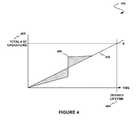
- FIG. 4shows an integration-based technique 400 for delaying operations that reduce a lifetime of memory, in accordance with still yet another embodiment.
- the present technique 400may be implemented to carry out the method 100 of FIG. 1 and/or further in the context of the techniques 200 and 300 of FIGS. 2-3 .
- the technique 400may be implemented in any desired environment.
- the aforementioned definitionsmay apply during the present description.
- the technique 400takes into account a total number of operations 402 that result in the memory exhibiting a minimal degree of usability, as well as a minimum desired lifetime 404 of the memory. From such data points, a maximum average operation rate 406 may be calculated that achieves the minimum desired lifetime 404 . In use, a number of lifetime-reducing operations may be monitored as time progresses.
- any excess operationsare not necessarily delayed in an unconditional manner (like the technique 200 of FIG. 2 ). Instead, such excess operations may be conditionally delayed based on an integral function reflecting use of the memory.
- an integral of a difference between the overall rate of lifetime-reducing operations over time, and the maximum average operation rate 406may be calculated on an on-going basis. To this end, if such, integration indicates that such operations may exceed maximum average operation rate 406 , the aforementioned delaying need not necessarily occur.
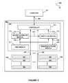
- FIG. 5illustrates a system 500 for delaying operations that reduce a lifetime of memory, if a desired lifetime duration exceeds an estimated lifetime duration, in accordance with another embodiment.
- the present system 500may be implemented to carry out the method 100 of FIG. 1 and/or further optionally incorporate any of the techniques of FIGS. 2-4 .
- the system 500may be used in any desired manner.
- a storage system 503that comprises a plurality of storage devices 530 , 540 .
- At least one storage bus 502couples at least one controller 511 with at least one computer 501 .
- the storage bus 502may include, but is not limited to a serial advanced technology attachment (SATA) bus, serial attached SCSI (SAS) bus, fiber channel bus, memory bus interface, flash memory bus, NAND flash bus, integrated drive electronics (IDE) bus, advanced technology attachment (ATA) bus, consumer electronics (CE) bus, universal serial bus (USB) bus, smart card bus, multimedia card (MMC) bus, etc.
- the controller 511is capable of being coupled between a system (e.g. computer 501 ) and secondary storage (such as at least one of the storage devices 530 , 540 ).
- at least one apparatus 510for prolonging a lifetime of memory associated with the storage devices 530 , 540 .
- the apparatus 510includes a controller 511 coupled to the storage devices 530 , 540 via a plurality of corresponding buses 521 , 522 , respectively.
- the controller 511uses a plurality of buses 521 , 522 to control and exchange data with a plurality of storage devices 530 , 540 in order to execute commands received from the computer 501 via the storage bus 502 .
- the storage devices 530 , 540each include at least one module or block 531 , 532 , 533 , 541 , 542 , 543 for storing data.
- At least a portion of the aforementioned commandsare lifetime-reducing commands that have a negative impact on at least one module or block 531 , 532 , 533 , 541 , 542 , 543 .
- the apparatus 510serves for prolonging the lifetime of the storage devices 530 , 540 , despite such lifetime-reducing commands.
- the controller 511is coupled to a lifetime estimator module 514 via a corresponding bus 512 .
- the apparatus 510further includes a time module 517 coupled to the lifetime estimator module 514 via a bus 518 , for providing a current time.
- the lifetime estimator module 514serves to receive commands communicated to the controller 511 from the computer 501 via the storage bus 502 . Further, the lifetime estimator module 514 computes an estimated lifetime assuming mat the command(s) received through the bus 512 was executed.
- the lifetime estimator module 514is coupled to a throttling module 516 via a bus 515 .
- the lifetime estimator module 514uses the bus 515 to pass to the throttling module 516 the estimated lifetime for a command currently executed by the controller 511 .
- the currently executed commandmay, in one embodiment, be the same as that received by the lifetime estimator module 514 via the bus 512 and may further be the same as that received by the controller 511 from the computer 501 via the storage bus 502 .
- the current time module 517is also coupled to the throttling module 516 via the bus 518 .
- the current time from the current time module 517may be passed to the throttling module 516 as well.
- the current time module 517may be implemented, for example, as a simple counter incrementing at a constant time interval, etc.
- the throttling module 516is former coupled with a required lifetime module 520 via a bus 519 , as well as to the controller 511 via a bus 513 .
- the required lifetime module 520is adapted for storing a desired lifetime.
- the throttling module 516maybe configured to pass information to the controller 511 via the bus 513 to instruct the controller 511 to delay the execution of the current command.
- the throttling module 516 of the apparatus 510may operate such that the execution of the current command is delayed until the effects of the execution on the lifetime is such that the estimated lifetime is longer or the same as the required lifetime stored in the required lifetime module 520 .
- the functionality of the throttling module 516may, in one embodiment, be as simple as providing a delay signal to the controller 511 , if the estimated lifetime received via the bus 515 is shorter than the required lifetime received via the bus 519 .
- the above-described functions of the controller 511 , the lifetime estimator module 514 , and the throttling module 516may be applied to a group of commands received in predefined time intervals. Such arrangement may allow the system 500 to meet the required lifetime without unnecessarily throttling short bursts of commands that would otherwise reduce lifetime.
- the time intervalfor example, as being one day, such a technique allows the system 500 to provide higher instantaneous performance for lifetime-reducing commands because, during some period of the day (e.g. nighttime, etc.), there may be intervals of time where there is a reduced frequency of lifetime-reducing commands compared to an average frequency of lifetime-reducing commands.
- coherencymay be maintained over time.
- lifetime-reducing command Ais delayed, then all commands (lifetime-reducing or not) that depend on the data of A or the values resulting from the execution of the command A are also delayed.
- timemay be replaced with various approximations of time, such as time that a disk is being powered up.
- the computer 501 , a RAID controller, and/or other devicemay provide additional information to increase precision of time tracked.
- the time counteris not counting. Since real time is advancing, this may unnecessarily reduce performance.
- the computer 501 , software, and/or a controllermay provide information about the time when the system 500 is turned off, for addressing such issue.
- the system 500may be equipped with an intra-storage device redundancy capability for reducing cost and improving performance.
- datamay be moved between the individual storage devices 530 , 540 , based on any aspect associated with a lifetime thereof (e.g. see, for example, operation 102 of FIG. 1 , etc.). For instance, a situation may involve a first one of the storage devices 530 including a set of data that is more frequently overwritten with respect to the data of a second one of the storage devices 540 .
- such datamay be moved from the first storage device 530 to the second storage device 540 , and henceforth the first storage device 530 or one or more blocks/modules 531 , 532 , 533 thereof may be used to store less-frequently written data or retired from further use.
- storage device wearmay be distributed appropriately to avoid one storage device from failing at a point in time that is vastly premature with respect to other storage devices of the group.
- the present techniquemay be applied not only among different storage devices, but also portions thereof.
- the lifetime of any memory componentsmay be managed in such a manner.
- the controller 511may thus be equipped for reducing and/or distributing writes. By this feature, a lifetime of the appropriate storage devices 530 , 540 may be prolonged.
- One exemplary method for carrying out such techniquewill now be set forth during the description of FIG. 6 .
- FIG. 6illustrates a method 600 for delaying operations that reduce a lifetime of memory, if a desired lifetime duration exceeds an estimated lifetime duration, in accordance with another embodiment.
- the present method 600may be carried out using the system 500 of FIG. 5 and/or further optionally incorporate any of the techniques of FIGS. 1-4 .
- the method 600may be used in any desired manner. Still yet, the aforementioned definitions may apply during the present description.
- the method 600continues by a controller (e.g. controller 511 of FIG. 5 , etc.) awaits a command 602 issued by a computer (e.g. computer 501 , etc.) to at least one storage device (e.g. storage device 530 , 540 , etc.).
- a controllere.g. controller 511 of FIG. 5 , etc.
- the methodproceeds to decision 603 , when the controller determines if the command accepted in operation 602 is a lifetime-reducing command (e.g. an erase operation, a write operation, etc.). If it is determined in decision 603 that the currently received command is not lifetime-reducing, such command may be simply processed per operation 607 .
- a lifetime-reducing commande.g. an erase operation, a write operation, etc.
- an estimated lifetimeis computed by a lifetime estimator module (e.g. lifetime estimator module 514 , etc.) based on the command received in operation 602 , a previous lifetime, and a current time (e.g. via time module 517 , etc.). See operation 604 .
- the previous lifetimemay represent a previous state of the lifetime estimator module.
- the previous lifetimemay be obtained by measuring one or more properties of at least one storage device.
- the lifetime estimated by such lifetime estimator moduleis then provided to a throttling module (e.g. throttling module 516 , etc.).
- a throttling modulee.g. throttling module 516 , etc.
- the throttling moduledetermines that throttling is necessary if the estimated lifetime received from the lifetime estimator is shorter than the required lifetime sent to the throttling module. If throttling is necessary, the method 600 proceeds in operation 606 by delaying (e.g. throttling, etc.) the lifetime-reducing command. However, if the estimated lifetime is not shorter than the required lifetime, the method 600 proceeds in operation 607 , as set forth above.
- the throttling modulemay throttle execution of the lifetime-reducing commands using the controller.
- such throttlingmay be implemented by delaying execution of the lifetime-reducing command using the controller, until the lifetime estimated by the lifetime estimator is longer or the same as the required lifetime.
- the throttlingmay be determined in predetermined periods of time and applied to commands in a subsequent predetermined time period.
- a limitmay be applied as to how much lifetime may be shortened within a predetermined time interval.
- a limit as to how much a lifetime may be shortened within a time intervalmay be determined in one or more previous time intervals.
- the throttlingmay be determined based on an analysis of a plurality of pending operations, allowing non-lifetime-reducing operations to be performed ahead of lifetime-reducing operations or operations that depend on such lifetime-reducing operations.
- a data storage systemmay be provided that controls lifetime-reducing operations to guarantee a required minimal lifetime.
- the impact of lifetime-reducing operations on such minimal required lifetimemay thus be estimated, and a frequency of the lifetime-reducing operations may be adaptively constrained.
- FIG. 7shows a graphical user interface 700 for gauging a lifetime of memory, in accordance with another embodiment.
- the present graphical user interface 700may be implemented in the context of the functionality and architecture of FIGS. 1-6 .
- the graphical user interface 700may be used in any desired environment.
- the aforementioned definitionsmay apply during the present description.
- various indiciamay be displayed reflecting at least one aspect associated with a lifetime of memory.
- such aspectmay be that identified in operation 102 of FIG. 1 .
- this lifetime-related aspectmay include any desired aspect that is at least partially related to the lifetime of the memory.
- the aspectmay be retrieved by the controller 511 from any of the modules shown for being processed and/or simply passed to the computer 501 which may, in turn, display associated indicia under the control of a software application program (e.g. plug-in, etc.).
- the aforementioned indiciamay, in one embodiment, include a gauge 702 for indicating an amount of lifetime remaining for one or more memories.
- the gauge 702may indicate an amount of total memory lifetime remaining as a function of the number of lifetime-reducing operations that have been performed over time.
- the aforementioned indiciamay include a estimation 705 for indicating a lifetime based on extrapolation of prior usage and assuming suspension of throttling operations.
- the aforementioned indiciamay include a warning 704 for indicating that a minimum amount of lifetime remains for one or more memories. Such lifetime may be estimated, for example, based on historical memory usage data. By this design, a user may he warned of a situation where memory should be replaced within a predetermined amount of time, etc. Of course, other embodiments are contemplated where any desired indicia is used to report various information in association with a lifetime of memory.
- FIG. 8shows a method 800 for reducing write operations in memory, utilizing difference information, in accordance with another embodiment.
- the present method 800may or may not be carried out in conjunction with the functionality and architecture of FIGS. 1-7 .
- the method 800may be carried out in any desired environment. It should also be noted that the aforementioned definitions may apply during the present description.
- write operations to be performed on data stored in memoryare identified. See operation 802 .
- write operationsmay include any operations that result in the data stored in the memory being modified.
- write operationsmay be identified in any desired manner by intercepting write commands associated such operations, the write operations themselves, etc.
- a differenceis then determined between results of the write operations and the data stored in the memory.
- the aforementioned differencemay reflect, at least in part, any difference between a first state of the data stored in the memory, and a second state that would result from the foregoing write operations.
- a differencemay be determined between any data stored in the memory. For example, a new modified version of a file may be created and written to a new location in the memory, such that a difference in data from different locations in the memory may be determined. As an option, the location of the data may be identified based on a hash, bloom filters, etc. To this end, in one exemplary embodiment where different instances of the same data are written to different locations in the memory, the determined difference may include the location of the data, and not necessarily the data itself.
- difference information associated with the differencemay be stored in the memory (e.g. the same memory in which the data is stored, etc.). In another embodiment, the difference information may also be stored in a separate buffer, in a manner that will be elaborated upon later during the description of a different embodiment. It should be noted that the difference information may include any information that describes, at least in part, the difference determined in operation 804 . As will soon become apparent during the discussion of a later described embodiment, the difference information may, in one embodiment, be stored utilizing an instruction set. As also described below, such instruction set may adaptively change and/or dynamically expand, in various embodiments.
- the write operationsmay be reduced, utilizing the difference information. See operation 806 .
- reduction in write operationsmay optionally result in a prolonged lifetime of the memory.
- FIG. 9illustrates a system 900 for reducing write operations in memory, in accordance with another embodiment.
- the present system 900may be implemented to carry out the method 800 of FIG. 8 and/or further optionally incorporate any of the methods or techniques of FIGS. 1-7 .
- the system 900may be used in any desired manner. Yet again, the aforementioned definitions may apply during the present description.
- the system 900includes a computer 901 coupled to a storage device 930 via an input/output (I/O) bus 902 , in a manner that will soon be set forth.
- the I/O bus 902includes a read path 903 and a write path 904 .
- the storage device 930includes a plurality of storage blocks 931 , 932 , 933 .
- the storage blocks 931 , 932 , 933are written and read by the computer 901 .
- a predetermined portion 934 of each of the storage blocks 931 , 932 , 933may be allocated to store difference information that reflects any changes made to data stored in the remaining portion 935 of the corresponding storage block 931 , 932 , 933 by the computer 901 .
- a size of the predetermined portion 934may be user configured.
- the difference information stored thereinmay take any form.
- Table 1illustrates one possible format for representing an instance of difference information (a plurality of which may be stored in each predetermined portion 934 of the storage blocks 931 , 932 , 933 ).
- the operation codemay represent an operation to be performed on the data stored in the remaining portion 935 of the corresponding storage block 931 , 932 , 933 .
- operationsmay include, but are not limited to end, replace, move up, move down, delete, insert, and/or any other operation, for that matter.
- the source starting address and sizemay point to and indicate the size (respectively) of the data stored in the remaining portion 935 of the corresponding storage block 931 , 932 , 933 which is to be the subject of the operation.
- dataitself may be stored as a component of the difference information.
- a compression algorithmmay be applied to the difference information for more efficient storage.
- a source location of the datamay be designated, and not necessarily the data itself, since such data is contained in an original storage block.
- new operationsmay be adaptively created. For example, repeating sequences of a first operation may be replaced by a new second operation. Such new second operation may optionally describe a sequence of the first operation. In this way, new operations may be adaptively created such that the system 900 may optimally adapt itself to new applications.
- Table 1is set forth for illustrative purposes only and should not be construed as limiting in any manner whatsoever.
- an instance of difference informationmay simply include the data to be replaced (without any complex commands, etc.).
- Such apparatus 910includes a coalescing memory 920 including a plurality of coalescing buffers 921 , 922 , 923 .
- a size of each of the coalescing buffers 921 , 922 , 923may be of a predetermined size (e.g. 4 Kb, etc.) that may correlate with a minimum block portion that may be written to each of the storage blocks 931 , 932 , 933 in a single operation.
- the coalescing buffers 921may include on-chip storage, external memory, DRAM, SRAM, etc.
- the coalescing memory buffers 921 , 922 , 923each hold an instance of difference information (e.g. see Table 1, for example) for the corresponding storage blocks 931 , 932 , and 933 .
- a first one of the coalescing memory buffers 921holds an instance of difference information for a first one of the storage blocks 931
- a second one of the coalescing memory buffers 922holds an instance of difference information for a second one of the storage blocks 932
- a third one of the coalescing memory buffers 923holds an instance of difference information for a third one of the storage blocks 933 , and so on.
- the apparatus 910further includes an update module 912 coupled to the coalescing memory 920 via a bus 914 for writing the difference information stored in the coalescing memory buffers 921 , 922 , 923 to the corresponding storage blocks 931 , 932 , and 933 .
- such writemay be initiated upon one of the coalescing memory buffers 921 , 922 , 923 being filled with at least one instance of difference information (and thus constituting a minimum write size to the appropriate one of the storage blocks 931 , 932 , and 933 ).
- the update module 912is coupled to the storage device 930 via a bus 915 .
- an output of the update module 912is coupled to the I/O bus 902 via the read path 903 .
- a difference computation module 911is coupled to the update module 912 via the read path bus 903 , coupled to the I/O bus 902 via the write path bus 904 , and further coupled to the coalescing memory 920 via a bus 913 .
- the difference computation module 911is capable of reading data from the storage device 938 and further reconstructing a current state of such data using the difference information from the associated storage block 931 , 932 , and 933 ; and/or coalescing memory buffers 921 , 922 , 923 .
- the difference computation module 911is further capable of writing data to the storage device 930 by first reconstructing a current state of such data (similar to the read operation above), identifying a difference between such current state and a state that would result after a write operation (initiated by the computer 901 ), and populating the coalescing memory buffers 921 , 922 , 923 with one or more instances of difference information to be used to update the associated storage block 931 , 932 , and 933 , as appropriate. More information regarding such read and write operations will now be set forth during the description of FIGS. 10 and 11 .
- the difference computation module 911may employ any desired technique for identifying the aforementioned difference(s). For example, various string matching algorithms, data motion estimation techniques, etc. may be utilized, for example. In still additional embodiments, the differences may be determined on a byte-by-byte basis.
- computation of the differencemay involve any one or more of the following: finding what byte strings are inserted, finding what byte strings are deleted, finding what byte strings are replaced, finding what byte strings are copied, determining if byte strings are updated by adding values, finding copies of storage blocks and creating references to them, finding block splits, finding block merges, etc.
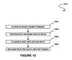
- FIG. 10illustrates a method 1000 for reading memory using difference information, in accordance with one embodiment.
- the present method 1000may be carried out using the system 900 of FIG. 9 and/or further optionally incorporate any of the techniques of FIGS. 1-8 , as desired.
- the method 1000may be used in any desired manner. Still yet, the aforementioned definitions may apply during the present description.
- the method 1000may begin in operation 1001 by reading blocks (e.g. blocks 931 , 932 , 933 of FIG. 9 , etc.) from storage (e.g. storage device 930 , etc.), as requested by a computer (e.g. computer 901 , etc.).
- the read storage blocks dataare then sent to an update module (e.g. update module 912 , etc.).
- difference informationis read from coalescing buffers (e.g. coalescing buffers 921 , 922 , 923 , etc.) corresponding to the storage blocks (associated with the computer request), and/or from the storage blocks themselves. See operation 1002 .
- the appropriate source of the difference informationmay depend on whether the required information has been written from the coalescing buffers to the corresponding storage blocks at the time of the read request.
- the difference informationmay be interspersed between data in flash.
- differences relating to particular datamay be grouped into one or more groups.
- the update moduleapplies the differences reflected in the difference information from operation 1002 on corresponding blocks read in operation 1001 .
- the data reconstructed in operation 1003may be sent to the computer via a read path (e.g. read path 903 , etc.). See operation 1004 .
- the foregoing data read operationmay involve mapping from a logical storage block number to a physical storage block number. Still yet, the method 1000 may further provide error detection and error correction in conjunction with the read. Such error detection and correction of read data may further include a re-read operation in an attempt to recover data, and relocate the recovered data to another storage location. For example, such relocation of recovered data may involve logical storage block translation and/or be based on error rate information of candidate storage blocks.
- FIG. 11illustrates a method 1100 for writing memory using difference information, in accordance with one embodiment.
- the present method 1100may be carried out using the system 900 of FIG. 9 and/or further optionally incorporate any of the techniques of FIGS. 1-8 , 10 , as desired.
- the method 1100may be used in any desired manner. Still yet, the aforementioned definitions may apply during the present description.
- the method 1100may begin in operation 1101 by reading blocks (e.g. blocks 931 , 932 , 933 of FIG. 9 , etc.) from storage (e.g. storage device 930 , etc.), which are subject to a write request by a computer (e.g. computer 901 , etc.).
- the read storage blocks dataare then sent to an update module (e.g. update module 912 , etc.).
- update modulee.g. update module 912 , etc.
- difference informationis read from the coalescing buffers (e.g. coalescing buffers 921 , 922 , 923 , etc.) corresponding to the storage blocks (associated with the computer request), and/or from the storage blocks themselves.
- the update moduleapplies the differences reflected in the difference information from operation 1102 on corresponding blocks read in operation 1101 , to reconstruct the data to be read or written.
- the data reconstructed in operation 1103may be sent to a difference computation module (e.g. difference computation module 911 , etc.) and compared with a state of the data that would result from execution of the write operation requested by the computer. See operation 1104 .
- a difference between the reconstructed data and the state of the data that would result from execution of the write operationis identified.
- such differencemay be caused by an application (running on the computer) for updating the data.
- Such updatesmay include, but are not limited to replacing a string of bytes, inserting a string of bytes, deleting a string of bytes, copying a string of bytes, etc.
- difference information associated with the differences computed in operation 1104may be appended to the appropriate coalescing buffers corresponding to blocks for which there is at least one difference computed in operation 1104 .
- Such appendingmay be accomplished writing to the end of the coalesce buffers in the coalescing memory.
- such appendingmay further include decompressing a coalesce buffer, appending the data, and recompressing the appropriate coalesce buffer.
- coalescing buffer memorymay be reallocated to the coalescing buffers on demand.
- the difference informationmay be stored as operations describing functions (e.g. writes, etc.) performed on the data.
- the difference informationmay reflect changes resultant from operations performed in a B-Tree and may thus represent differences with respect to such operations.
- B-Treesmay optionally be utilized by databases, mail-servers, file systems, etc.
- coalesce buffersare tested to determine whether they are full. If no coalesce buffer is full, the method 1100 proceeds to operation 1110 . If, on the other hand, at least one coalesce buffer is full, the method 1100 proceeds to operation 1107 . In operation 1107 , any full coalesce buffers are appended to the difference information. In addition, such full coalesce buffers are emptied (for reuse, etc.), as shown in operation 1112 .
- the method 1100proceeds to operation 1110 if it is determined that difference information is not full. However, in response to a determination that the difference information is full, changes from the difference information are applied on the data. Note operation 1116 . Moreover, the block of data with the applied changes is written and old data is discarded, as shown in operation 1118 . Still yet, as shown in operation 1120 , the difference information is emptied.
- a data storage systemmay be provided which uses differences between written and existing data to reduce writes and to distribute writes across memory blocks to improve reliability of block based storage.
- the memory mentioned in the foregoing embodimentsmay include a mechanical storage device (e.g. a disk drive including a SATA disk drive, a SAS disk drive, a fiber channel disk drive, IDE disk drive, ATA disk drive, CE disk drive, USB disk drive, smart card disk drive, MMC disk drive, etc.) and/or a non-mechanical storage device (e.g. semiconductor-based, etc.).
- a mechanical storage devicee.g. a disk drive including a SATA disk drive, a SAS disk drive, a fiber channel disk drive, IDE disk drive, ATA disk drive, CE disk drive, USB disk drive, smart card disk drive, MMC disk drive, etc.
- non-mechanical storage devicee.g. semiconductor-based, etc.
- Such non-mechanical memorymay, for example, include volatile or non-volatile memory.
- the nonvolatile memory devicemay include flash memory (e.g.
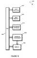
- FIG. 12illustrates an exemplary system 1200 in which the various architecture and/or functionality of the various previous embodiments may be implemented.
- the exemplary system 1200may represent the computer set forth in some of the previous embodiments.
- the various apparatuses set forth abovemay even be a component of the system 1200 .
- a system 1200including at least one host processor 1201 which is connected to a communication bus 1202 .
- the system 1200also includes a main memory 1204 .
- Control logic (software) and dataare stored in the main memory 1204 which may take the form of random access memory (RAM).
- RAMrandom access memory
- the system 1200also includes a graphics processor 1206 and a display 1208 , i.e. a computer monitor.
- the system 1200may also include a secondary storage 1210 .
- the secondary storage 1210includes, for example, a hard disk drive and/or a removable storage drive, representing a floppy disk drive, a magnetic tape drive, a compact disk drive, etc.
- the removable storage drivereads from and/or writes to a removable storage module in a well known manner.
- Computer programs, or computer control logic algorithmsmay be stored in the main memory 1204 and/or the secondary storage 1210 . Such computer programs, when executed, enable the system 1200 to perform various functions. Memory 1204 , storage 1210 and/or any other storage are possible examples of computer-readable media.
- the architecture and/or functionality of the various previous figuresmay be implemented in the context of the host processor 1201 , graphics processor 1206 , secondary storage 1210 , an integrated circuit (not shown) that is capable of at least a portion of the capabilities of both the host processor 1201 and the graphics processor 1206 , a chipset (i.e. a group of integrated circuits designed to work and be sold as a module for performing related functions, etc.), and/or any other integrated circuit for that matter.
- a chipseti.e. a group of integrated circuits designed to work and be sold as a module for performing related functions, etc.
- the architecture and/or functionality of the various previous figuresmay be implemented in the context of a general computer system, a circuit board system, a game console system dedicated for entertainment purposes, an application-specific system, and/or any other desired system.
- the system 1200may take the form of a desktop computer, lap-top computer, and/or any other type of logic.
- the system 1200may take the form of various other devices including, but not limited to a personal digital assistant (PDA) device, a mobile phone device, a television, etc.
- PDApersonal digital assistant
- system 1200may be coupled to a network [e.g. a telecommunications network, local area network (LAN), wireless network, wide area network (WAN) such as the Internet, peer-to-peer network, cable network, etc.] for communication purposes.
- a networke.g. a telecommunications network, local area network (LAN), wireless network, wide area network (WAN) such as the Internet, peer-to-peer network, cable network, etc.
Landscapes
- Engineering & Computer Science (AREA)
- Theoretical Computer Science (AREA)
- Physics & Mathematics (AREA)
- General Engineering & Computer Science (AREA)
- General Physics & Mathematics (AREA)
- Techniques For Improving Reliability Of Storages (AREA)
Abstract
Description
| TABLE 1 | |||
| Operation | Source Starting | ||
| Code | Address | Size | Data |
| END | N/A | N/A | N/A |
| Replace | <address> | <byte length> | <replacement data> |
| Move Up | <address> | <byte length> | <address from where data |
| is to be moved> | |||
| Move | <address> | <byte length> | <address from where |
| Down | data is to be moved> | ||
| Insert | <address> | <byte length> | <data to be inserted> |
| Delete | <address> | <byte length> | N/A |
Claims (19)
Priority Applications (9)
| Application Number | Priority Date | Filing Date | Title |
|---|---|---|---|
| US11/852,117US7747813B2 (en) | 2006-11-24 | 2007-09-07 | Multi-memory device system and method for managing a lifetime thereof |
| CN200780043176.3ACN101578587B (en) | 2006-11-24 | 2007-11-21 | Operation for delaying the reduction of lifetime of memory |
| JP2009538408AJP5171840B2 (en) | 2006-11-24 | 2007-11-21 | Method and storage system for delaying operation to shorten memory life |
| PCT/US2007/024295WO2008063647A2 (en) | 2006-11-24 | 2007-11-21 | Delaying an operation that reduces a lifetime of memory |
| TW096144306ATWI475569B (en) | 2006-11-24 | 2007-11-22 | System, method, and computer program product for delaying an operation that reduces a lifetime of memory |
| US12/822,442US8230164B2 (en) | 2006-11-24 | 2010-06-24 | Techniques for multi-memory device lifetime management |
| JP2012243564AJP5448013B2 (en) | 2006-11-24 | 2012-11-05 | System, method, and computer program product for delaying operations that reduce memory life |
| JP2013261095AJP5814335B2 (en) | 2006-11-24 | 2013-12-18 | Reduction of writing and estimation and display of remaining life of nonvolatile memory |
| JP2013261097AJP2014078262A (en) | 2006-11-24 | 2013-12-18 | Techniques for multi-memory device lifetime management |
Applications Claiming Priority (3)
| Application Number | Priority Date | Filing Date | Title |
|---|---|---|---|
| US86084306P | 2006-11-24 | 2006-11-24 | |
| US87824207P | 2007-01-03 | 2007-01-03 | |
| US11/852,117US7747813B2 (en) | 2006-11-24 | 2007-09-07 | Multi-memory device system and method for managing a lifetime thereof |
Related Child Applications (1)
| Application Number | Title | Priority Date | Filing Date |
|---|---|---|---|
| US12/822,442ContinuationUS8230164B2 (en) | 2006-11-24 | 2010-06-24 | Techniques for multi-memory device lifetime management |
Publications (2)
| Publication Number | Publication Date |
|---|---|
| US20080126720A1 US20080126720A1 (en) | 2008-05-29 |
| US7747813B2true US7747813B2 (en) | 2010-06-29 |
Family
ID=39465153
Family Applications (2)
| Application Number | Title | Priority Date | Filing Date |
|---|---|---|---|
| US11/852,117Expired - Fee RelatedUS7747813B2 (en) | 2006-11-24 | 2007-09-07 | Multi-memory device system and method for managing a lifetime thereof |
| US12/822,442Expired - Fee RelatedUS8230164B2 (en) | 2006-11-24 | 2010-06-24 | Techniques for multi-memory device lifetime management |
Family Applications After (1)
| Application Number | Title | Priority Date | Filing Date |
|---|---|---|---|
| US12/822,442Expired - Fee RelatedUS8230164B2 (en) | 2006-11-24 | 2010-06-24 | Techniques for multi-memory device lifetime management |
Country Status (1)
| Country | Link |
|---|---|
| US (2) | US7747813B2 (en) |
Cited By (15)
| Publication number | Priority date | Publication date | Assignee | Title |
|---|---|---|---|---|
| US20100146187A1 (en)* | 2008-12-05 | 2010-06-10 | Grimsrud Knut S | Endurance management technique |
| US20100325340A1 (en)* | 2009-06-23 | 2010-12-23 | Seagate Technology Llc | Memory Wear Control |
| US20110016233A1 (en)* | 2009-07-17 | 2011-01-20 | Ross John Stenfort | System, method, and computer program product for inserting a gap in information sent from a drive to a host device |
| US8516166B2 (en) | 2009-07-20 | 2013-08-20 | Lsi Corporation | System, method, and computer program product for reducing a rate of data transfer to at least a portion of memory |
| US20140136771A1 (en)* | 2007-04-25 | 2014-05-15 | Apple Inc. | Initiating Memory Wear Leveling |
| US8904093B1 (en) | 2012-06-15 | 2014-12-02 | Juniper Networks, Inc. | Managing lifetime of limited usage storage devices in a caching system |
| US8954689B2 (en) | 2011-06-30 | 2015-02-10 | Seagate Technology Llc | Limiting activity rates that impact life of a data storage media |
| US9372628B1 (en) | 2015-01-23 | 2016-06-21 | International Business Machines Corporation | Deduplication tracking for accurate lifespan prediction |
| US9934174B2 (en) | 2015-09-18 | 2018-04-03 | Seagate Technology Llc | Selectively enable data transfer based on accrued data credits |
| US11347639B1 (en)* | 2013-01-28 | 2022-05-31 | Radian Memory Systems, Inc. | Nonvolatile memory controller with host targeted erase and data copying based upon wear |
| US11416413B1 (en) | 2014-09-09 | 2022-08-16 | Radian Memory Systems, Inc. | Storage system with division based addressing and cooperative flash management |
| US11487656B1 (en) | 2013-01-28 | 2022-11-01 | Radian Memory Systems, Inc. | Storage device with multiplane segments and cooperative flash management |
| US11740801B1 (en) | 2013-01-28 | 2023-08-29 | Radian Memory Systems, Inc. | Cooperative flash management of storage device subdivisions |
| US12292792B1 (en) | 2019-12-09 | 2025-05-06 | Radian Memory Systems, LLC | Erasure coding techniques for flash memory |
| US12367138B1 (en) | 2024-01-10 | 2025-07-22 | Sandisk Technologies Inc. | Method to extend the lifespan of a data storage device by repurposing blocks from burst pool |
Families Citing this family (40)
| Publication number | Priority date | Publication date | Assignee | Title |
|---|---|---|---|---|
| US7809900B2 (en)* | 2006-11-24 | 2010-10-05 | Sandforce, Inc. | System, method, and computer program product for delaying an operation that reduces a lifetime of memory |
| US7904619B2 (en) | 2006-11-24 | 2011-03-08 | Sandforce, Inc. | System, method, and computer program product for reducing memory write operations using difference information |
| US7747813B2 (en)* | 2006-11-24 | 2010-06-29 | Sandforce, Inc. | Multi-memory device system and method for managing a lifetime thereof |
| US7903486B2 (en) | 2007-11-19 | 2011-03-08 | Sandforce, Inc. | System, method, and computer program product for increasing a lifetime of a plurality of blocks of memory |
| US8554983B2 (en)* | 2008-05-27 | 2013-10-08 | Micron Technology, Inc. | Devices and methods for operating a solid state drive |
| JP2010238124A (en)* | 2009-03-31 | 2010-10-21 | Fujitsu Ltd | Data management program, data management apparatus, and data management method |
| US8725931B1 (en) | 2010-03-26 | 2014-05-13 | Western Digital Technologies, Inc. | System and method for managing the execution of memory commands in a solid-state memory |
| US8782327B1 (en) | 2010-05-11 | 2014-07-15 | Western Digital Technologies, Inc. | System and method for managing execution of internal commands and host commands in a solid-state memory |
| US9026716B2 (en) | 2010-05-12 | 2015-05-05 | Western Digital Technologies, Inc. | System and method for managing garbage collection in solid-state memory |
| US8862806B2 (en) | 2010-08-20 | 2014-10-14 | Samsung Electronics Co., Ltd | Semiconductor storage device and method of throttling performance of the same |
| US9037778B2 (en)* | 2010-08-20 | 2015-05-19 | Samsung Electronics Co., Ltd. | Method and apparatus to interface semiconductor storage device and host to provide performance throttling of semiconductor storage device |
| KR101702392B1 (en) | 2010-08-20 | 2017-02-06 | 삼성전자주식회사 | Semiconductor storage device and method for throttling performance of the semiconductor storage device |
| US9021192B1 (en) | 2010-09-21 | 2015-04-28 | Western Digital Technologies, Inc. | System and method for enhancing processing of memory access requests |
| US9164886B1 (en) | 2010-09-21 | 2015-10-20 | Western Digital Technologies, Inc. | System and method for multistage processing in a memory storage subsystem |
| WO2012157029A1 (en)* | 2011-05-19 | 2012-11-22 | Hitachi, Ltd. | Storage control apparatus and management method for semiconductor-type storage device |
| US9098399B2 (en) | 2011-08-31 | 2015-08-04 | SMART Storage Systems, Inc. | Electronic system with storage management mechanism and method of operation thereof |
| US9063844B2 (en) | 2011-09-02 | 2015-06-23 | SMART Storage Systems, Inc. | Non-volatile memory management system with time measure mechanism and method of operation thereof |
| US9021319B2 (en) | 2011-09-02 | 2015-04-28 | SMART Storage Systems, Inc. | Non-volatile memory management system with load leveling and method of operation thereof |
| US9239781B2 (en) | 2012-02-07 | 2016-01-19 | SMART Storage Systems, Inc. | Storage control system with erase block mechanism and method of operation thereof |
| US9671962B2 (en) | 2012-11-30 | 2017-06-06 | Sandisk Technologies Llc | Storage control system with data management mechanism of parity and method of operation thereof |
| US9123445B2 (en) | 2013-01-22 | 2015-09-01 | SMART Storage Systems, Inc. | Storage control system with data management mechanism and method of operation thereof |
| US9329928B2 (en) | 2013-02-20 | 2016-05-03 | Sandisk Enterprise IP LLC. | Bandwidth optimization in a non-volatile memory system |
| US9214965B2 (en) | 2013-02-20 | 2015-12-15 | Sandisk Enterprise Ip Llc | Method and system for improving data integrity in non-volatile storage |
| US9183137B2 (en)* | 2013-02-27 | 2015-11-10 | SMART Storage Systems, Inc. | Storage control system with data management mechanism and method of operation thereof |
| JP6005566B2 (en) | 2013-03-18 | 2016-10-12 | 株式会社東芝 | Information processing system, control program, and information processing apparatus |
| US9170941B2 (en) | 2013-04-05 | 2015-10-27 | Sandisk Enterprises IP LLC | Data hardening in a storage system |
| US10049037B2 (en) | 2013-04-05 | 2018-08-14 | Sandisk Enterprise Ip Llc | Data management in a storage system |
| US9543025B2 (en) | 2013-04-11 | 2017-01-10 | Sandisk Technologies Llc | Storage control system with power-off time estimation mechanism and method of operation thereof |
| US10546648B2 (en) | 2013-04-12 | 2020-01-28 | Sandisk Technologies Llc | Storage control system with data management mechanism and method of operation thereof |
| US9367353B1 (en) | 2013-06-25 | 2016-06-14 | Sandisk Technologies Inc. | Storage control system with power throttling mechanism and method of operation thereof |
| US9244519B1 (en) | 2013-06-25 | 2016-01-26 | Smart Storage Systems. Inc. | Storage system with data transfer rate adjustment for power throttling |
| US9146850B2 (en) | 2013-08-01 | 2015-09-29 | SMART Storage Systems, Inc. | Data storage system with dynamic read threshold mechanism and method of operation thereof |
| US9431113B2 (en) | 2013-08-07 | 2016-08-30 | Sandisk Technologies Llc | Data storage system with dynamic erase block grouping mechanism and method of operation thereof |
| US9448946B2 (en) | 2013-08-07 | 2016-09-20 | Sandisk Technologies Llc | Data storage system with stale data mechanism and method of operation thereof |
| US9361222B2 (en) | 2013-08-07 | 2016-06-07 | SMART Storage Systems, Inc. | Electronic system with storage drive life estimation mechanism and method of operation thereof |
| US9152555B2 (en) | 2013-11-15 | 2015-10-06 | Sandisk Enterprise IP LLC. | Data management with modular erase in a data storage system |
| US9348520B2 (en) | 2014-03-24 | 2016-05-24 | Western Digital Technologies, Inc. | Lifetime extension of non-volatile semiconductor memory for data storage device |
| US9690696B1 (en) | 2014-05-14 | 2017-06-27 | Western Digital Technologies, Inc. | Lifetime extension of memory for data storage system |
| US9785374B2 (en) | 2014-09-25 | 2017-10-10 | Microsoft Technology Licensing, Llc | Storage device management in computing systems |
| US20170131947A1 (en)* | 2015-11-06 | 2017-05-11 | Pho Hoang | Data and collection methods to analyze life acceleration of SSD with real usages |
Citations (30)
| Publication number | Priority date | Publication date | Assignee | Title |
|---|---|---|---|---|
| US5485595A (en) | 1993-03-26 | 1996-01-16 | Cirrus Logic, Inc. | Flash memory mass storage architecture incorporating wear leveling technique without using cam cells |
| US5544356A (en) | 1990-12-31 | 1996-08-06 | Intel Corporation | Block-erasable non-volatile semiconductor memory which tracks and stores the total number of write/erase cycles for each block |
| US5568626A (en) | 1990-02-27 | 1996-10-22 | Nec Corporation | Method and system for rewriting data in a non-volatile memory a predetermined large number of times |
| US5568423A (en) | 1995-04-14 | 1996-10-22 | Unisys Corporation | Flash memory wear leveling system providing immediate direct access to microprocessor |
| US5621687A (en) | 1995-05-31 | 1997-04-15 | Intel Corporation | Programmable erasure and programming time for a flash memory |
| US5819307A (en) | 1994-10-20 | 1998-10-06 | Fujitsu Limited | Control method in which frequency of data erasures is limited |
| US5835935A (en) | 1995-09-13 | 1998-11-10 | Lexar Media, Inc. | Method of and architecture for controlling system data with automatic wear leveling in a semiconductor non-volatile mass storage memory |
| US5881229A (en) | 1995-04-26 | 1999-03-09 | Shiva Corporation | Method and product for enchancing performance of computer networks including shared storage objects |
| US5956473A (en) | 1996-11-25 | 1999-09-21 | Macronix International Co., Ltd. | Method and system for managing a flash memory mass storage system |
| US5963970A (en) | 1996-12-20 | 1999-10-05 | Intel Corporation | Method and apparatus for tracking erase cycles utilizing active and inactive wear bar blocks having first and second count fields |
| US6000006A (en) | 1997-08-25 | 1999-12-07 | Bit Microsystems, Inc. | Unified re-map and cache-index table with dual write-counters for wear-leveling of non-volatile flash RAM mass storage |
| US6154808A (en) | 1997-10-31 | 2000-11-28 | Fujitsu Limited | Method and apparatus for controlling data erase operations of a non-volatile memory device |
| US6230233B1 (en) | 1991-09-13 | 2001-05-08 | Sandisk Corporation | Wear leveling techniques for flash EEPROM systems |
| US6405295B1 (en) | 1999-09-07 | 2002-06-11 | Oki Electric Industry, Co., Ltd. | Data storage apparatus for efficient utilization of limited cycle memory material |
| US6539453B1 (en) | 1998-12-22 | 2003-03-25 | Gemplus | Storage system including means for management of a memory with anti-attrition, and process of anti-attrition management of a memory |
| US6694402B1 (en) | 1998-09-04 | 2004-02-17 | Hyperstone Ag | Access control for a memory having a limited erasure frequency |
| US6732221B2 (en) | 2001-06-01 | 2004-05-04 | M-Systems Flash Disk Pioneers Ltd | Wear leveling of static areas in flash memory |
| US6831865B2 (en) | 2002-10-28 | 2004-12-14 | Sandisk Corporation | Maintaining erase counts in non-volatile storage systems |
| US6914853B2 (en) | 2001-09-27 | 2005-07-05 | Intel Corporation | Mechanism for efficient wearout counters in destructive readout memory |
| US6925523B2 (en) | 2003-03-03 | 2005-08-02 | Agilent Technologies, Inc. | Managing monotonically increasing counter values to minimize impact on non-volatile storage |
| US6948026B2 (en) | 2001-08-24 | 2005-09-20 | Micron Technology, Inc. | Erase block management |
| US6973531B1 (en) | 2002-10-28 | 2005-12-06 | Sandisk Corporation | Tracking the most frequently erased blocks in non-volatile memory systems |
| US6985992B1 (en) | 2002-10-28 | 2006-01-10 | Sandisk Corporation | Wear-leveling in non-volatile storage systems |
| US7000063B2 (en) | 2001-10-05 | 2006-02-14 | Matrix Semiconductor, Inc. | Write-many memory device and method for limiting a number of writes to the write-many memory device |
| US7032087B1 (en) | 2003-10-28 | 2006-04-18 | Sandisk Corporation | Erase count differential table within a non-volatile memory system |
| US7035967B2 (en) | 2002-10-28 | 2006-04-25 | Sandisk Corporation | Maintaining an average erase count in a non-volatile storage system |
| US7096313B1 (en) | 2002-10-28 | 2006-08-22 | Sandisk Corporation | Tracking the least frequently erased blocks in non-volatile memory systems |
| US7103732B1 (en) | 2002-10-28 | 2006-09-05 | Sandisk Corporation | Method and apparatus for managing an erase count block |
| US7120729B2 (en) | 2002-10-28 | 2006-10-10 | Sandisk Corporation | Automated wear leveling in non-volatile storage systems |
| US7555575B2 (en)* | 2006-07-27 | 2009-06-30 | Hitachi, Ltd. | Method and apparatus for migrating data between storage volumes of different data pattern |
Family Cites Families (72)
| Publication number | Priority date | Publication date | Assignee | Title |
|---|---|---|---|---|
| US563970A (en)* | 1896-07-14 | keyes | ||
| US5768182A (en)* | 1991-05-21 | 1998-06-16 | The Regents Of The University Of California | Ferroelectric nonvolatile dynamic random access memory device |
| TW261687B (en)* | 1991-11-26 | 1995-11-01 | Hitachi Seisakusyo Kk | |
| US6347051B2 (en)* | 1991-11-26 | 2002-02-12 | Hitachi, Ltd. | Storage device employing a flash memory |
| JP2610737B2 (en)* | 1991-12-20 | 1997-05-14 | シャープ株式会社 | Recording and playback device |
| US5592415A (en)* | 1992-07-06 | 1997-01-07 | Hitachi, Ltd. | Non-volatile semiconductor memory |
| JP3641280B2 (en)* | 1992-10-30 | 2005-04-20 | インテル・コーポレーション | Method for determining blocks to be cleaned up in a flash EEPROM array |
| US5337275A (en)* | 1992-10-30 | 1994-08-09 | Intel Corporation | Method for releasing space in flash EEPROM memory array to allow the storage of compressed data |
| US6085248A (en)* | 1997-02-11 | 2000-07-04 | Xaqtu Corporation | Media access control transmitter and parallel network management system |
| US6305014B1 (en)* | 1998-06-18 | 2001-10-16 | International Business Machines Corporation | Lifetime-sensitive instruction scheduling mechanism and method |
| US6145069A (en)* | 1999-01-29 | 2000-11-07 | Interactive Silicon, Inc. | Parallel decompression and compression system and method for improving storage density and access speed for non-volatile memory and embedded memory devices |
| US6314026B1 (en)* | 1999-02-08 | 2001-11-06 | Kabushiki Kaisha Toshiba | Nonvolatile semiconductor device using local self boost technique |
| US7628622B2 (en)* | 1999-08-04 | 2009-12-08 | Super Talent Electronics, Inc. | Multi-level cell (MLC) slide flash memory |
| US7130807B1 (en)* | 1999-11-22 | 2006-10-31 | Accenture Llp | Technology sharing during demand and supply planning in a network-based supply chain environment |
| US6484228B2 (en)* | 2000-04-19 | 2002-11-19 | Motorola, Inc. | Method and apparatus for data compression and decompression for a data processor system |
| JP2001306543A (en)* | 2000-04-19 | 2001-11-02 | Nec Corp | Microcomputer, and data reloading method for flash memory |
| US6256232B1 (en)* | 2000-07-07 | 2001-07-03 | Institute For Information Industry | Data access method capable of reducing the number of erasing to flash memory and data patch and access device using the same |
| TW520514B (en)* | 2001-08-02 | 2003-02-11 | Macronix Int Co Ltd | Circuit and method of qualification test for non-volatile memory |
| US20030120841A1 (en)* | 2001-12-21 | 2003-06-26 | Chang Matthew C.T. | System and method of data logging |
| US6735673B2 (en)* | 2002-01-10 | 2004-05-11 | Hewlett-Packard Development Company, L.P. | Apparatus and methods for cache line compression |
| US6640283B2 (en)* | 2002-01-16 | 2003-10-28 | Hewlett-Packard Development Company, L.P. | Apparatus for cache compression engine for data compression of on-chip caches to increase effective cache size |
| US6606273B1 (en)* | 2002-04-11 | 2003-08-12 | Advanced Micro Devices, Inc. | Methods and systems for flash memory tunnel oxide reliability testing |
| US6775751B2 (en)* | 2002-08-06 | 2004-08-10 | International Business Machines Corporation | System and method for using a compressed main memory based on degree of compressibility |
| NZ520786A (en)* | 2002-08-14 | 2005-06-24 | Daniel James Oaeconnell | Method of booting a computer system using a memory image of the post boot content of the system RAM memory |
| KR100484485B1 (en)* | 2002-10-01 | 2005-04-20 | 한국전자통신연구원 | Method for storing data in non-volatile memory and apparatus therefor |
| US6910106B2 (en)* | 2002-10-04 | 2005-06-21 | Microsoft Corporation | Methods and mechanisms for proactive memory management |
| US20040135903A1 (en)* | 2002-10-11 | 2004-07-15 | Brooks Lane C. | In-stream lossless compression of digital image sensor data |
| CA2408979A1 (en)* | 2002-10-18 | 2004-04-18 | Richard Egon Schauble | Tamper-evident use-indicating odometer and engine-timer |
| US7320100B2 (en)* | 2003-05-20 | 2008-01-15 | Cray Inc. | Apparatus and method for memory with bit swapping on the fly and testing |
| US7143238B2 (en)* | 2003-09-30 | 2006-11-28 | Intel Corporation | Mechanism to compress data in a cache |
| US20070067366A1 (en)* | 2003-10-08 | 2007-03-22 | Landis John A | Scalable partition memory mapping system |
| US7480760B2 (en)* | 2003-12-17 | 2009-01-20 | Wegener Communications, Inc. | Rotational use of memory to minimize write cycles |
| JP4357304B2 (en)* | 2004-01-09 | 2009-11-04 | 株式会社バッファロー | External storage device |
| US7222214B2 (en)* | 2004-03-25 | 2007-05-22 | Lucent Technologies Inc. | Device-level address translation within a programmable non-volatile memory device |
| US7595796B2 (en)* | 2004-04-23 | 2009-09-29 | Hewlett-Packard Development Company, L.P. | Optimizing lifetime of a display |
| US7316563B2 (en) | 2004-07-30 | 2008-01-08 | Marshall Daniel S | Combustor with integrated counter-flow heat exchanger |
| US7664796B2 (en)* | 2004-10-13 | 2010-02-16 | Microsoft Corporation | Electronic labeling for offline management of storage devices |
| US20060112113A1 (en)* | 2004-11-08 | 2006-05-25 | Jinsheng Gu | Static file system differencing and updating |
| US7433994B2 (en)* | 2004-12-07 | 2008-10-07 | Ocz Technology Group, Inc. | On-device data compression to increase speed and capacity of flash memory-based mass storage devices |
| US7224604B2 (en)* | 2005-03-14 | 2007-05-29 | Sandisk Il Ltd. | Method of achieving wear leveling in flash memory using relative grades |
| US20060209684A1 (en)* | 2005-03-18 | 2006-09-21 | Via Technologies, Inc. | Data rate controller, and method of control thereof |
| US7206230B2 (en)* | 2005-04-01 | 2007-04-17 | Sandisk Corporation | Use of data latches in cache operations of non-volatile memories |
| US7457178B2 (en)* | 2006-01-12 | 2008-11-25 | Sandisk Corporation | Trimming of analog voltages in flash memory devices |
| US20070180186A1 (en)* | 2006-01-27 | 2007-08-02 | Cornwell Michael J | Non-volatile memory management |
| US8848789B2 (en)* | 2006-03-27 | 2014-09-30 | Qualcomm Incorporated | Method and system for coding and decoding information associated with video compression |
| US7653778B2 (en)* | 2006-05-08 | 2010-01-26 | Siliconsystems, Inc. | Systems and methods for measuring the useful life of solid-state storage devices |
| US8412682B2 (en)* | 2006-06-29 | 2013-04-02 | Netapp, Inc. | System and method for retrieving and using block fingerprints for data deduplication |
| US7561482B2 (en)* | 2006-09-07 | 2009-07-14 | Sandisk Corporation | Defective block isolation in a non-volatile memory system |
| US7904764B2 (en)* | 2006-11-24 | 2011-03-08 | Sandforce, Inc. | Memory lifetime gauging system, method and computer program product |
| WO2008063647A2 (en) | 2006-11-24 | 2008-05-29 | Sandforce Inc. | Delaying an operation that reduces a lifetime of memory |
| US7747813B2 (en)* | 2006-11-24 | 2010-06-29 | Sandforce, Inc. | Multi-memory device system and method for managing a lifetime thereof |
| US20080126685A1 (en)* | 2006-11-24 | 2008-05-29 | Radoslav Danilak | System, method, and computer program product for reducing memory write operations using an instruction set |
| US7809900B2 (en)* | 2006-11-24 | 2010-10-05 | Sandforce, Inc. | System, method, and computer program product for delaying an operation that reduces a lifetime of memory |
| US7904619B2 (en)* | 2006-11-24 | 2011-03-08 | Sandforce, Inc. | System, method, and computer program product for reducing memory write operations using difference information |
| US8090980B2 (en)* | 2006-12-08 | 2012-01-03 | Sandforce, Inc. | System, method, and computer program product for providing data redundancy in a plurality of storage devices |
| US7904672B2 (en)* | 2006-12-08 | 2011-03-08 | Sandforce, Inc. | System and method for providing data redundancy after reducing memory writes |
| KR20080090021A (en) | 2007-04-03 | 2008-10-08 | 삼성테크윈 주식회사 | Data storage module having interfaces with different data rates and data transmission method thereof |
| US20080294813A1 (en)* | 2007-05-24 | 2008-11-27 | Sergey Anatolievich Gorobets | Managing Housekeeping Operations in Flash Memory |
| TW200917123A (en)* | 2007-10-03 | 2009-04-16 | Guo-Lang Zhang | USB flash disk for computer boot up and method of loading programs in the USB flash disk |
| TWI373772B (en)* | 2007-10-04 | 2012-10-01 | Phison Electronics Corp | Wear leveling method and controller using the same |
| US20090125645A1 (en)* | 2007-11-12 | 2009-05-14 | Gemalto Inc | System and method for supporting multiple tokens having a smart card to control parameters of a flash memory device |
| US7903486B2 (en)* | 2007-11-19 | 2011-03-08 | Sandforce, Inc. | System, method, and computer program product for increasing a lifetime of a plurality of blocks of memory |
| US7849275B2 (en) | 2007-11-19 | 2010-12-07 | Sandforce, Inc. | System, method and a computer program product for writing data to different storage devices based on write frequency |
| US7870105B2 (en)* | 2007-11-20 | 2011-01-11 | Hitachi, Ltd. | Methods and apparatus for deduplication in storage system |
| US9183133B2 (en) | 2007-11-28 | 2015-11-10 | Seagate Technology Llc | System, method, and computer program product for increasing spare space in memory to extend a lifetime of the memory |
| US8321625B2 (en)* | 2007-12-05 | 2012-11-27 | Densbits Technologies Ltd. | Flash memory device with physical cell value deterioration accommodation and methods useful in conjunction therewith |
| US7827320B1 (en)* | 2008-03-28 | 2010-11-02 | Western Digital Technologies, Inc. | Serial ATA device implementing intra-command processing by detecting XRDY primitive while in the XRDY state |
| US7970978B2 (en)* | 2008-05-27 | 2011-06-28 | Initio Corporation | SSD with SATA and USB interfaces |
| US20100017650A1 (en)* | 2008-07-19 | 2010-01-21 | Nanostar Corporation, U.S.A | Non-volatile memory data storage system with reliability management |
| US8140739B2 (en)* | 2008-08-08 | 2012-03-20 | Imation Corp. | Flash memory based storage devices utilizing magnetoresistive random access memory (MRAM) to store files having logical block addresses stored in a write frequency file buffer table |
| US8291131B2 (en)* | 2009-07-06 | 2012-10-16 | Micron Technology, Inc. | Data transfer management |
| US8516166B2 (en) | 2009-07-20 | 2013-08-20 | Lsi Corporation | System, method, and computer program product for reducing a rate of data transfer to at least a portion of memory |
- 2007
- 2007-09-07USUS11/852,117patent/US7747813B2/ennot_activeExpired - Fee Related
- 2010
- 2010-06-24USUS12/822,442patent/US8230164B2/ennot_activeExpired - Fee Related
Patent Citations (30)
| Publication number | Priority date | Publication date | Assignee | Title |
|---|---|---|---|---|
| US5568626A (en) | 1990-02-27 | 1996-10-22 | Nec Corporation | Method and system for rewriting data in a non-volatile memory a predetermined large number of times |
| US5544356A (en) | 1990-12-31 | 1996-08-06 | Intel Corporation | Block-erasable non-volatile semiconductor memory which tracks and stores the total number of write/erase cycles for each block |
| US6230233B1 (en) | 1991-09-13 | 2001-05-08 | Sandisk Corporation | Wear leveling techniques for flash EEPROM systems |
| US5485595A (en) | 1993-03-26 | 1996-01-16 | Cirrus Logic, Inc. | Flash memory mass storage architecture incorporating wear leveling technique without using cam cells |
| US5819307A (en) | 1994-10-20 | 1998-10-06 | Fujitsu Limited | Control method in which frequency of data erasures is limited |
| US5568423A (en) | 1995-04-14 | 1996-10-22 | Unisys Corporation | Flash memory wear leveling system providing immediate direct access to microprocessor |
| US5881229A (en) | 1995-04-26 | 1999-03-09 | Shiva Corporation | Method and product for enchancing performance of computer networks including shared storage objects |
| US5621687A (en) | 1995-05-31 | 1997-04-15 | Intel Corporation | Programmable erasure and programming time for a flash memory |
| US5835935A (en) | 1995-09-13 | 1998-11-10 | Lexar Media, Inc. | Method of and architecture for controlling system data with automatic wear leveling in a semiconductor non-volatile mass storage memory |
| US5956473A (en) | 1996-11-25 | 1999-09-21 | Macronix International Co., Ltd. | Method and system for managing a flash memory mass storage system |
| US5963970A (en) | 1996-12-20 | 1999-10-05 | Intel Corporation | Method and apparatus for tracking erase cycles utilizing active and inactive wear bar blocks having first and second count fields |
| US6000006A (en) | 1997-08-25 | 1999-12-07 | Bit Microsystems, Inc. | Unified re-map and cache-index table with dual write-counters for wear-leveling of non-volatile flash RAM mass storage |
| US6154808A (en) | 1997-10-31 | 2000-11-28 | Fujitsu Limited | Method and apparatus for controlling data erase operations of a non-volatile memory device |
| US6694402B1 (en) | 1998-09-04 | 2004-02-17 | Hyperstone Ag | Access control for a memory having a limited erasure frequency |
| US6539453B1 (en) | 1998-12-22 | 2003-03-25 | Gemplus | Storage system including means for management of a memory with anti-attrition, and process of anti-attrition management of a memory |
| US6405295B1 (en) | 1999-09-07 | 2002-06-11 | Oki Electric Industry, Co., Ltd. | Data storage apparatus for efficient utilization of limited cycle memory material |
| US6732221B2 (en) | 2001-06-01 | 2004-05-04 | M-Systems Flash Disk Pioneers Ltd | Wear leveling of static areas in flash memory |
| US6948026B2 (en) | 2001-08-24 | 2005-09-20 | Micron Technology, Inc. | Erase block management |
| US6914853B2 (en) | 2001-09-27 | 2005-07-05 | Intel Corporation | Mechanism for efficient wearout counters in destructive readout memory |
| US7000063B2 (en) | 2001-10-05 | 2006-02-14 | Matrix Semiconductor, Inc. | Write-many memory device and method for limiting a number of writes to the write-many memory device |
| US6973531B1 (en) | 2002-10-28 | 2005-12-06 | Sandisk Corporation | Tracking the most frequently erased blocks in non-volatile memory systems |
| US6985992B1 (en) | 2002-10-28 | 2006-01-10 | Sandisk Corporation | Wear-leveling in non-volatile storage systems |
| US6831865B2 (en) | 2002-10-28 | 2004-12-14 | Sandisk Corporation | Maintaining erase counts in non-volatile storage systems |
| US7035967B2 (en) | 2002-10-28 | 2006-04-25 | Sandisk Corporation | Maintaining an average erase count in a non-volatile storage system |
| US7096313B1 (en) | 2002-10-28 | 2006-08-22 | Sandisk Corporation | Tracking the least frequently erased blocks in non-volatile memory systems |
| US7103732B1 (en) | 2002-10-28 | 2006-09-05 | Sandisk Corporation | Method and apparatus for managing an erase count block |
| US7120729B2 (en) | 2002-10-28 | 2006-10-10 | Sandisk Corporation | Automated wear leveling in non-volatile storage systems |
| US6925523B2 (en) | 2003-03-03 | 2005-08-02 | Agilent Technologies, Inc. | Managing monotonically increasing counter values to minimize impact on non-volatile storage |
| US7032087B1 (en) | 2003-10-28 | 2006-04-18 | Sandisk Corporation | Erase count differential table within a non-volatile memory system |
| US7555575B2 (en)* | 2006-07-27 | 2009-06-30 | Hitachi, Ltd. | Method and apparatus for migrating data between storage volumes of different data pattern |
Non-Patent Citations (4)
| Title |
|---|
| U.S. Appl. No. 11/852,082, filed Sep. 7, 2007. |
| U.S. Appl. No. 11/852,104, filed Sep. 7, 2007. |
| U.S. Appl. No. 11/852,129, filed Sep. 7, 2007. |
| U.S. Appl. No. 11/852,138, filed Sep. 7, 2007. |
Cited By (39)
| Publication number | Priority date | Publication date | Assignee | Title |
|---|---|---|---|---|
| US20140136771A1 (en)* | 2007-04-25 | 2014-05-15 | Apple Inc. | Initiating Memory Wear Leveling |
| US9110787B2 (en)* | 2007-04-25 | 2015-08-18 | Apple Inc. | Initiating memory wear leveling |
| US20100146187A1 (en)* | 2008-12-05 | 2010-06-10 | Grimsrud Knut S | Endurance management technique |
| US20100325340A1 (en)* | 2009-06-23 | 2010-12-23 | Seagate Technology Llc | Memory Wear Control |
| US8732389B2 (en) | 2009-06-23 | 2014-05-20 | Seagate Technology Llc | Memory wear control |
| US9274712B2 (en) | 2009-06-23 | 2016-03-01 | Seagate Technology Llc | Memory wear control |
| US20110016233A1 (en)* | 2009-07-17 | 2011-01-20 | Ross John Stenfort | System, method, and computer program product for inserting a gap in information sent from a drive to a host device |
| US8140712B2 (en) | 2009-07-17 | 2012-03-20 | Sandforce, Inc. | System, method, and computer program product for inserting a gap in information sent from a drive to a host device |
| US8516166B2 (en) | 2009-07-20 | 2013-08-20 | Lsi Corporation | System, method, and computer program product for reducing a rate of data transfer to at least a portion of memory |
| US8954689B2 (en) | 2011-06-30 | 2015-02-10 | Seagate Technology Llc | Limiting activity rates that impact life of a data storage media |
| US8904093B1 (en) | 2012-06-15 | 2014-12-02 | Juniper Networks, Inc. | Managing lifetime of limited usage storage devices in a caching system |
| US11740801B1 (en) | 2013-01-28 | 2023-08-29 | Radian Memory Systems, Inc. | Cooperative flash management of storage device subdivisions |
| US11868247B1 (en) | 2013-01-28 | 2024-01-09 | Radian Memory Systems, Inc. | Storage system with multiplane segments and cooperative flash management |
| US12164421B1 (en) | 2013-01-28 | 2024-12-10 | Radian Memory Systems, LLC | Storage device with erase units written using a common page offset |
| US11347639B1 (en)* | 2013-01-28 | 2022-05-31 | Radian Memory Systems, Inc. | Nonvolatile memory controller with host targeted erase and data copying based upon wear |
| US11347638B1 (en)* | 2013-01-28 | 2022-05-31 | Radian Memory Systems, Inc. | Nonvolatile memory controller with data relocation and host-triggered erase |
| US11354234B1 (en)* | 2013-01-28 | 2022-06-07 | Radian Memory Systems, Inc. | Memory controller for nonvolatile memory with targeted erase from host and write destination selection based on wear |
| US11354235B1 (en)* | 2013-01-28 | 2022-06-07 | Radian Memory Systems, Inc. | Memory controller for nonvolatile memory that tracks data write age and fulfills maintenance requests targeted to host-selected memory space subset |
| US12147335B1 (en) | 2013-01-28 | 2024-11-19 | Radian Memory Systems, LLC | Cooperative storage device for managing logical subdivisions |
| US12093533B1 (en) | 2013-01-28 | 2024-09-17 | Radian Memory Systems, Inc. | Memory management of nonvolatile discrete namespaces |
| US11487656B1 (en) | 2013-01-28 | 2022-11-01 | Radian Memory Systems, Inc. | Storage device with multiplane segments and cooperative flash management |
| US11487657B1 (en) | 2013-01-28 | 2022-11-01 | Radian Memory Systems, Inc. | Storage system with multiplane segments and cooperative flash management |
| US11899575B1 (en) | 2013-01-28 | 2024-02-13 | Radian Memory Systems, Inc. | Flash memory system with address-based subdivision selection by host and metadata management in storage drive |
| US11544183B1 (en)* | 2013-01-28 | 2023-01-03 | Radian Memory Systems, Inc. | Nonvolatile memory controller host-issued address delimited erasure and memory controller remapping of host-address space for bad blocks |
| US11640355B1 (en) | 2013-01-28 | 2023-05-02 | Radian Memory Systems, Inc. | Storage device with multiplane segments, cooperative erasure, metadata and flash management |
| US11681614B1 (en) | 2013-01-28 | 2023-06-20 | Radian Memory Systems, Inc. | Storage device with subdivisions, subdivision query, and write operations |
| US11704237B1 (en) | 2013-01-28 | 2023-07-18 | Radian Memory Systems, Inc. | Storage system with multiplane segments and query based cooperative flash management |
| US11762766B1 (en) | 2013-01-28 | 2023-09-19 | Radian Memory Systems, Inc. | Storage device with erase unit level address mapping |
| US11748257B1 (en) | 2013-01-28 | 2023-09-05 | Radian Memory Systems, Inc. | Host, storage system, and methods with subdivisions and query based write operations |
| US11537528B1 (en) | 2014-09-09 | 2022-12-27 | Radian Memory Systems, Inc. | Storage system with division based addressing and query based cooperative flash management |
| US11914523B1 (en) | 2014-09-09 | 2024-02-27 | Radian Memory Systems, Inc. | Hierarchical storage device with host controlled subdivisions |
| US11449436B1 (en) | 2014-09-09 | 2022-09-20 | Radian Memory Systems, Inc. | Storage system with division based addressing and cooperative flash management |
| US11416413B1 (en) | 2014-09-09 | 2022-08-16 | Radian Memory Systems, Inc. | Storage system with division based addressing and cooperative flash management |
| US12306766B1 (en) | 2014-09-09 | 2025-05-20 | Radian Memory Systems, ILLC | Hierarchical storage device with host controlled subdivisions |
| US9372628B1 (en) | 2015-01-23 | 2016-06-21 | International Business Machines Corporation | Deduplication tracking for accurate lifespan prediction |
| US9495106B2 (en) | 2015-01-23 | 2016-11-15 | International Business Machines Corporation | Deduplication tracking for accurate lifespan prediction |
| US9934174B2 (en) | 2015-09-18 | 2018-04-03 | Seagate Technology Llc | Selectively enable data transfer based on accrued data credits |
| US12292792B1 (en) | 2019-12-09 | 2025-05-06 | Radian Memory Systems, LLC | Erasure coding techniques for flash memory |
| US12367138B1 (en) | 2024-01-10 | 2025-07-22 | Sandisk Technologies Inc. | Method to extend the lifespan of a data storage device by repurposing blocks from burst pool |
Also Published As
| Publication number | Publication date |
|---|---|
| US8230164B2 (en) | 2012-07-24 |
| US20080126720A1 (en) | 2008-05-29 |
| US20110125956A1 (en) | 2011-05-26 |
Similar Documents
| Publication | Publication Date | Title |
|---|---|---|
| US10732857B2 (en) | Techniques for reducing memory write operations using coalescing memory buffers and difference information | |
| US7747813B2 (en) | Multi-memory device system and method for managing a lifetime thereof | |
| US7809900B2 (en) | System, method, and computer program product for delaying an operation that reduces a lifetime of memory | |
| US8171356B2 (en) | Reducing writes, and estimating and displaying estimated remaining lifetime of non-volatile memories | |
| US10318181B2 (en) | System, method, and computer program product for increasing spare space in memory to extend a lifetime of the memory | |
| US20080126685A1 (en) | System, method, and computer program product for reducing memory write operations using an instruction set | |
| WO2008063647A9 (en) | Delaying an operation that reduces a lifetime of memory | |
| US10282127B2 (en) | Managing data in a storage system | |
| HK1151365A (en) | Increasing spare space in memory to extend a lifetime of the memory |
Legal Events
| Date | Code | Title | Description |
|---|---|---|---|
| AS | Assignment | Owner name:SANDFORCE, INC., CALIFORNIA Free format text:ASSIGNMENT OF ASSIGNORS INTEREST;ASSIGNOR:DANILAK, RADOSLAV;REEL/FRAME:019808/0717 Effective date:20070906 Owner name:SANDFORCE, INC.,CALIFORNIA Free format text:ASSIGNMENT OF ASSIGNORS INTEREST;ASSIGNOR:DANILAK, RADOSLAV;REEL/FRAME:019808/0717 Effective date:20070906 | |
| STCF | Information on status: patent grant | Free format text:PATENTED CASE | |
| AS | Assignment | Owner name:LSI CORPORATION, CALIFORNIA Free format text:ASSIGNMENT OF ASSIGNORS INTEREST;ASSIGNOR:SANDFORCE, INC.;REEL/FRAME:028434/0200 Effective date:20120104 | |
| FEPP | Fee payment procedure | Free format text:PAT HOLDER NO LONGER CLAIMS SMALL ENTITY STATUS, ENTITY STATUS SET TO UNDISCOUNTED (ORIGINAL EVENT CODE: STOL); ENTITY STATUS OF PATENT OWNER: LARGE ENTITY | |
| FPAY | Fee payment | Year of fee payment:4 | |
| AS | Assignment | Owner name:DEUTSCHE BANK AG NEW YORK BRANCH, AS COLLATERAL AG Free format text:PATENT SECURITY AGREEMENT;ASSIGNORS:LSI CORPORATION;AGERE SYSTEMS LLC;REEL/FRAME:032856/0031 Effective date:20140506 | |
| AS | Assignment | Owner name:AGERE SYSTEMS LLC, PENNSYLVANIA Free format text:TERMINATION AND RELEASE OF SECURITY INTEREST IN CERTAIN PATENTS INCLUDED IN SECURITY INTEREST PREVIOUSLY RECORDED AT REEL/FRAME (032856/0031);ASSIGNOR:DEUTSCHE BANK AG NEW YORK BRANCH, AS COLLATERAL AGENT;REEL/FRAME:034177/0257 Effective date:20140902 Owner name:LSI CORPORATION, CALIFORNIA Free format text:TERMINATION AND RELEASE OF SECURITY INTEREST IN CERTAIN PATENTS INCLUDED IN SECURITY INTEREST PREVIOUSLY RECORDED AT REEL/FRAME (032856/0031);ASSIGNOR:DEUTSCHE BANK AG NEW YORK BRANCH, AS COLLATERAL AGENT;REEL/FRAME:034177/0257 Effective date:20140902 | |
| AS | Assignment | Owner name:SEAGATE TECHNOLOGY LLC, CALIFORNIA Free format text:ASSIGNMENT OF ASSIGNORS INTEREST;ASSIGNOR:LSI CORPORATION;REEL/FRAME:034775/0777 Effective date:20140902 | |
| AS | Assignment | Owner name:AGERE SYSTEMS LLC, PENNSYLVANIA Free format text:TERMINATION AND RELEASE OF SECURITY INTEREST IN PATENT RIGHTS (RELEASES RF 032856-0031);ASSIGNOR:DEUTSCHE BANK AG NEW YORK BRANCH, AS COLLATERAL AGENT;REEL/FRAME:037684/0039 Effective date:20160201 Owner name:LSI CORPORATION, CALIFORNIA Free format text:TERMINATION AND RELEASE OF SECURITY INTEREST IN PATENT RIGHTS (RELEASES RF 032856-0031);ASSIGNOR:DEUTSCHE BANK AG NEW YORK BRANCH, AS COLLATERAL AGENT;REEL/FRAME:037684/0039 Effective date:20160201 | |
| MAFP | Maintenance fee payment | Free format text:PAYMENT OF MAINTENANCE FEE, 8TH YEAR, LARGE ENTITY (ORIGINAL EVENT CODE: M1552) Year of fee payment:8 | |
| FEPP | Fee payment procedure | Free format text:MAINTENANCE FEE REMINDER MAILED (ORIGINAL EVENT CODE: REM.); ENTITY STATUS OF PATENT OWNER: LARGE ENTITY | |
| LAPS | Lapse for failure to pay maintenance fees | Free format text:PATENT EXPIRED FOR FAILURE TO PAY MAINTENANCE FEES (ORIGINAL EVENT CODE: EXP.); ENTITY STATUS OF PATENT OWNER: LARGE ENTITY | |
| STCH | Information on status: patent discontinuation | Free format text:PATENT EXPIRED DUE TO NONPAYMENT OF MAINTENANCE FEES UNDER 37 CFR 1.362 | |
| FP | Lapsed due to failure to pay maintenance fee | Effective date:20220629 |