US7745934B2 - Integrated circuit and seed layers - Google Patents
Integrated circuit and seed layersDownload PDFInfo
- Publication number
- US7745934B2 US7745934B2US12/145,382US14538208AUS7745934B2US 7745934 B2US7745934 B2US 7745934B2US 14538208 AUS14538208 AUS 14538208AUS 7745934 B2US7745934 B2US 7745934B2
- Authority
- US
- United States
- Prior art keywords
- layer
- barrier
- adhesion layer
- adhesion
- conductive
- Prior art date
- Legal status (The legal status is an assumption and is not a legal conclusion. Google has not performed a legal analysis and makes no representation as to the accuracy of the status listed.)
- Expired - Fee Related
Links
Images


Classifications
- H—ELECTRICITY
- H01—ELECTRIC ELEMENTS
- H01L—SEMICONDUCTOR DEVICES NOT COVERED BY CLASS H10
- H01L21/00—Processes or apparatus adapted for the manufacture or treatment of semiconductor or solid state devices or of parts thereof
- H01L21/70—Manufacture or treatment of devices consisting of a plurality of solid state components formed in or on a common substrate or of parts thereof; Manufacture of integrated circuit devices or of parts thereof
- H01L21/71—Manufacture of specific parts of devices defined in group H01L21/70
- H01L21/768—Applying interconnections to be used for carrying current between separate components within a device comprising conductors and dielectrics
- H01L21/76838—Applying interconnections to be used for carrying current between separate components within a device comprising conductors and dielectrics characterised by the formation and the after-treatment of the conductors
- H01L21/76841—Barrier, adhesion or liner layers
- H01L21/76843—Barrier, adhesion or liner layers formed in openings in a dielectric
- H01L21/76846—Layer combinations
- H—ELECTRICITY
- H01—ELECTRIC ELEMENTS
- H01L—SEMICONDUCTOR DEVICES NOT COVERED BY CLASS H10
- H01L21/00—Processes or apparatus adapted for the manufacture or treatment of semiconductor or solid state devices or of parts thereof
- H01L21/70—Manufacture or treatment of devices consisting of a plurality of solid state components formed in or on a common substrate or of parts thereof; Manufacture of integrated circuit devices or of parts thereof
- H01L21/71—Manufacture of specific parts of devices defined in group H01L21/70
- H01L21/768—Applying interconnections to be used for carrying current between separate components within a device comprising conductors and dielectrics
- H01L21/76838—Applying interconnections to be used for carrying current between separate components within a device comprising conductors and dielectrics characterised by the formation and the after-treatment of the conductors
- H01L21/76841—Barrier, adhesion or liner layers
- H01L21/76843—Barrier, adhesion or liner layers formed in openings in a dielectric
- H01L21/76849—Barrier, adhesion or liner layers formed in openings in a dielectric the layer being positioned on top of the main fill metal
- H—ELECTRICITY
- H01—ELECTRIC ELEMENTS
- H01L—SEMICONDUCTOR DEVICES NOT COVERED BY CLASS H10
- H01L21/00—Processes or apparatus adapted for the manufacture or treatment of semiconductor or solid state devices or of parts thereof
- H01L21/70—Manufacture or treatment of devices consisting of a plurality of solid state components formed in or on a common substrate or of parts thereof; Manufacture of integrated circuit devices or of parts thereof
- H01L21/71—Manufacture of specific parts of devices defined in group H01L21/70
- H01L21/768—Applying interconnections to be used for carrying current between separate components within a device comprising conductors and dielectrics
- H01L21/76838—Applying interconnections to be used for carrying current between separate components within a device comprising conductors and dielectrics characterised by the formation and the after-treatment of the conductors
- H01L21/76841—Barrier, adhesion or liner layers
- H01L21/76853—Barrier, adhesion or liner layers characterized by particular after-treatment steps
- H01L21/76855—After-treatment introducing at least one additional element into the layer
- H01L21/76859—After-treatment introducing at least one additional element into the layer by ion implantation
- H—ELECTRICITY
- H01—ELECTRIC ELEMENTS
- H01L—SEMICONDUCTOR DEVICES NOT COVERED BY CLASS H10
- H01L21/00—Processes or apparatus adapted for the manufacture or treatment of semiconductor or solid state devices or of parts thereof
- H01L21/70—Manufacture or treatment of devices consisting of a plurality of solid state components formed in or on a common substrate or of parts thereof; Manufacture of integrated circuit devices or of parts thereof
- H01L21/71—Manufacture of specific parts of devices defined in group H01L21/70
- H01L21/768—Applying interconnections to be used for carrying current between separate components within a device comprising conductors and dielectrics
- H01L21/76838—Applying interconnections to be used for carrying current between separate components within a device comprising conductors and dielectrics characterised by the formation and the after-treatment of the conductors
- H01L21/76841—Barrier, adhesion or liner layers
- H01L21/76867—Barrier, adhesion or liner layers characterized by methods of formation other than PVD, CVD or deposition from a liquids
- H—ELECTRICITY
- H01—ELECTRIC ELEMENTS
- H01L—SEMICONDUCTOR DEVICES NOT COVERED BY CLASS H10
- H01L21/00—Processes or apparatus adapted for the manufacture or treatment of semiconductor or solid state devices or of parts thereof
- H01L21/70—Manufacture or treatment of devices consisting of a plurality of solid state components formed in or on a common substrate or of parts thereof; Manufacture of integrated circuit devices or of parts thereof
- H01L21/71—Manufacture of specific parts of devices defined in group H01L21/70
- H01L21/768—Applying interconnections to be used for carrying current between separate components within a device comprising conductors and dielectrics
- H01L21/76838—Applying interconnections to be used for carrying current between separate components within a device comprising conductors and dielectrics characterised by the formation and the after-treatment of the conductors
- H01L21/76841—Barrier, adhesion or liner layers
- H01L21/76871—Layers specifically deposited to enhance or enable the nucleation of further layers, i.e. seed layers
- H01L21/76874—Layers specifically deposited to enhance or enable the nucleation of further layers, i.e. seed layers for electroless plating
- H—ELECTRICITY
- H01—ELECTRIC ELEMENTS
- H01L—SEMICONDUCTOR DEVICES NOT COVERED BY CLASS H10
- H01L21/00—Processes or apparatus adapted for the manufacture or treatment of semiconductor or solid state devices or of parts thereof
- H01L21/70—Manufacture or treatment of devices consisting of a plurality of solid state components formed in or on a common substrate or of parts thereof; Manufacture of integrated circuit devices or of parts thereof
- H01L21/71—Manufacture of specific parts of devices defined in group H01L21/70
- H01L21/768—Applying interconnections to be used for carrying current between separate components within a device comprising conductors and dielectrics
- H01L21/76838—Applying interconnections to be used for carrying current between separate components within a device comprising conductors and dielectrics characterised by the formation and the after-treatment of the conductors
- H01L21/76885—By forming conductive members before deposition of protective insulating material, e.g. pillars, studs
- H—ELECTRICITY
- H01—ELECTRIC ELEMENTS
- H01L—SEMICONDUCTOR DEVICES NOT COVERED BY CLASS H10
- H01L2221/00—Processes or apparatus adapted for the manufacture or treatment of semiconductor or solid state devices or of parts thereof covered by H01L21/00
- H01L2221/10—Applying interconnections to be used for carrying current between separate components within a device
- H01L2221/1068—Formation and after-treatment of conductors
- H01L2221/1073—Barrier, adhesion or liner layers
- H01L2221/1084—Layers specifically deposited to enhance or enable the nucleation of further layers, i.e. seed layers
- H01L2221/1089—Stacks of seed layers
Definitions
- the present inventionrelates generally to integrated circuits. More particularly, it pertains to structures and methods for providing seed layers for integrated circuit metallurgy.
- 09/032,197which proposes a method using ionized sputtering to form the underlayer, then forming a low wetting layer on the areas where no copper is desired using jet vapor deposition.
- the copperis deposited with ionized Magnetron sputtering followed by hydrogen annealing. The excess copper is then removed by CMP as in the aforementioned application.
- FIG. 1A-1Killustrate one embodiment of the various processing steps for forming vias and metal lines according to the teachings of the present invention
- FIG. 2A-2Killustrate another embodiment of the various processing steps for forming vias and metal lines according to the teachings of the present invention
- FIG. 3A-3Killustrate another embodiment of the various processing steps for forming vias and metal lines according to the teachings of the present invention
- FIG. 4A-4Lillustrate another embodiment of the various processing steps for forming vias and metal lines according to the teachings of the present invention
- FIG. 5is an illustration of an integrated circuit formed according to the teachings of the present invention.
- FIG. 6illustrates an embodiment of a system including a portion of an integrated circuit formed according to any of the embodiments described in the present application.
- wafer and substrate used in the following descriptioninclude any structure having an exposed surface with which to form the integrated circuit (IC) structure of the invention.
- substrateis understood to include semiconductor wafers.
- substrateis also used to refer to semiconductor structures during processing, and may include other layers that have been fabricated thereupon.
- Substrateinclude doped and undoped semiconductors, epitaxial semiconductor layers supported by a base semiconductor or insulator, as well as other semiconductor structures well known to one skilled in the art.
- insulatoris defined to include any material that is less electrically conductive than the materials generally referred to as conductors by those skilled in the art. The following detailed description is, therefore, not to be taken in a limiting sense.
- the present inventionrequires only one complete CMP planarizing coupled with the formation of the first level vias, no matter how many levels of metallurgy are used. What are essentially cleanup CMP steps on each metal level are used in one process sequence.
- This processcan be used with an aluminum, copper, silver, gold or any other material which can subsequently be electrolessly plated or deposited by selective CVD or any other selective deposition process.
- a polyimide, other polymer or foam polymercan be used as an insulator. It can also be used with an oxide or other inorganic insulating structure if the insulating stack is compatible with the metal being used. It can also be used to form air bridge structures as well.
- the processuses low energy ion implantation to deposit both the adhesion and/or barrier layer along with the seed layer. This is coupled with using the resist layer which defines the damascene trench as the blocking layer to define the implant areas. Low energy implantation allows the placing of distinct layers of both barrier/adhesion and seed layers. The use of the same resist layers to define both the trench and seed layers allows a low cost implementation of the process.
- the structures and methods of embodiments of the present inventioninclude a diffusion barrier and a seed layer in an integrated circuit both formed using a low energy ion implantation followed by a selective deposition of metal lines for the integrated circuit.
- the selective deposition of the metal linesavoids the need for multiple chemical mechanical planarization (CMP) steps.
- CMPchemical mechanical planarization
- the low energy ion implantation of the present inventionallows for the distinct placement of both the diffusion barrier and the seed layer.
- a residual resistcan be used to remove the diffusion barrier and the seed layer from unwanted areas on a wafer surface.
- one illustrative embodiment of the present inventionincludes a method of making a diffusion barrier and a seed layer in an integrated circuit.
- the methodincludes patterning an insulator material to define a number of trenches in the insulator layer opening to a number of first level vias in a planarized surface.
- a barrier/adhesion layeris deposited in the number of trenches using a low energy ion implantation, e.g. a 100 to 800 electron volt (eV) ion implantation.
- a seed layeris deposited on the barrier/adhesion layer in the number of trenches also using the low energy ion implantation.
- This novel methodologyfurther accommodates the formation of aluminum, copper, gold, and/or silver metal interconnects.
- FIGS. 1A-1Killustrate a novel methodology for the formation of metal interconnects and/or a wiring structure in an integrated circuit according to the teachings of the present invention.
- the novel methodologyincludes the novel formation of a barrier/adhesion layer and a seed layer in an integrated circuit using a low energy ion implantation.
- the novel methodologyalso encompasses a novel method of making copper, silver, aluminum, or gold interconnect for an integrated circuit.
- FIG. 1Aillustrates a portion of an integrated circuit structure, namely an integrated circuit having a number of semiconductor devices formed in a substrate.
- FIG. 1illustrates the structure after a device structure is formed in the substrate and the contact structure to the device structure is in place.
- a number of semiconductor structurese.g. transistors
- FIG. 1Aillustrates the structure after a number of device structures, e.g. transistor 101 A and 101 B are formed in the substrate 100 .
- An insulator layer 102is deposited over the number of semiconductors 101 A and 101 B.
- the deposition of the insulator layer 102can include depositing a layer of Si 3 N 4 having a thickness in the range of 100 to 500 Angstroms ( ⁇ ). This insulator layer will also serve as an additional barrier to impurities coming from subsequent processing steps.
- Contact holes 105 A and 105 Bare opened to the number of device structures 101 A and 101 B using a photolithography technique.
- a photolithography techniqueOne of ordinary skill in the are will understand, upon reading this disclosure, the manner in which a photolithography technique can be used to create contact holes 105 A and 105 B.
- a titanium silicide liner 106 A and 106 Bis placed in the contact holes 105 A and 105 B, such a through a process such as chemical vapor deposition (CVD).
- CVDchemical vapor deposition
- tungsten vias 107 A and 107 Bcan be deposited in the contact holes 105 A and 105 B.
- the tungsten vias 107 A and 107 Bcan be deposited in the contact holes using any suitable technique such as using a CVD process.
- the excess tungstenis then removed from the wafer surface by chemical mechanical planarization (CMP) or other suitable processes to form a planarized surface 109 .
- CMPchemical mechanical planarization
- a first polymer layer 108is deposited over the wafer surface.
- the first polymer layer 108may be deposited using, for example, the process and material described in co-pending and commonly assigned application U.S. Ser. No. 09/128,859, entitled “Copper Metallurgy in Integrated Circuits,” which is hereby incorporated by reference.
- depositing a first polymer layer 108includes depositing a foamed polymer layer 108 .
- the first layer of polyimide 108is deposited and cured, forming a 5000 ⁇ thick layer of polymer 108 after curing.
- first layer of polyimide 108may also be deposited as suited for forming a first level metal pattern, the invention is not so limited.
- the first layer of polyimide 108 , or first insulator layer/material 108is patterned to define a number of trenches 110 in the first insulator layer 108 opening to a number of first level vias, e.g. tungsten vias 107 A and 107 B in planarized surface 109 .
- a first level metal pattern 110is defined in a mask layer of photoresist 112 and then the first layer of polyimide 108 is etched, using any suitable process, e.g. reactive ion etching (RIE), such that the first level metal pattern 110 is defined in the polyimide.
- RIEreactive ion etching
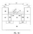
- a residual photoresist layer 112is left in place on the first insulator layer 108 in a number of region 113 outside of the number trenches 110 .
- FIG. 1BThe structure is now as appears in FIG. 1B .
- a first barrier/adhesion layer 114is deposited in the number of trenches 110 using a low energy ion implantation.
- depositing the barrier/adhesion layer 114includes depositing a layer of zirconium 114 having a thickness of approximately 5 to 100 ⁇ .
- depositing the barrier/adhesion layer 114includes depositing a barrier/adhesion layer 114 of titanium and/or hafnium.
- depositing the depositing a layer of zirconium 114includes depositing a layer of zirconium 114 having a thickness of approximately 50 ⁇ .
- the layer of zirconium 114is implanted at 100 electron volts (eV) into the surface of the trenches 110 in the polymer layer 108 using a varying angle implant ( ⁇ ), as represented by arrows 111 , where the angle of implantation is changed from normal to the wafer surface to 15 degrees off normal.
- eVelectron volts
- a first seed layer 116is deposited on the first barrier/adhesion layer 114 using a low energy ion implantation.
- depositing the seed layer 116 on the barrier/adhesion layer 114includes depositing a seed layer 116 selected from the group consisting of aluminum, copper, silver, and gold.
- depositing the seed layer 116includes depositing a layer of copper 116 having a thickness of approximately a 100 ⁇ . This can be achieved using an 8 ⁇ 10 16 ion implant of copper.
- using a low energy ion implantationincludes implanting the layer of copper 116 at 100 electron volts (eV) into the surface of the trenches 110 in the polymer layer. Also the layer of copper 116 is implanted at an angle normal to the wafer's surface, as shown by arrows 115 . As one of ordinary skill in the art will understand upon reading this disclosure, implanting the layer of copper 116 at an angle normal to the planarized surface results in the seed layer of copper 116 remaining on a bottom surface 118 in the number of trenches 110 and to a much lesser extent on the side surfaces 117 of the number of trenches 110 .
- eVelectron volts
- an optional layer of aluminum 121is deposited over the copper seed layer 116 again using a low energy ion implantation of 100 electron volts (eV).
- the optional layer of aluminum 121is deposited to have a thickness of approximately a 50 ⁇ . This can be achieved using a 3 ⁇ 10 16 ion implant of aluminum normal to the wafer surface.
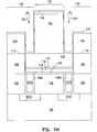
- the layer of aluminum 121is used to protect the copper seed layer 116 from oxidation prior to subsequent processing steps. The structure is now as shown in FIG. 1D .
- FIG. 1Eillustrates the structure after the next sequence of process steps.
- the residual photoresist layer 112has served as a blocking layer to define the implant areas for the barrier/adhesion layer 114 , the seed layer 116 , and the layer of aluminum 121 .
- the residual photoresist layer 112is now removed using a wet strip process, as the same will be understood by one of ordinary skill in the art upon reading this disclosure.
- removing the residual photoresist layer 112includes removing the unwanted aluminum layer 121 , the unwanted seed layer 116 , and the unwanted barrier/adhesion layer 114 from other areas of the wafer's surface, e.g., from over a number of regions 113 outside of the trenches 110 on a top surface 119 of the first insulator layer 108 .
- the structureis now as shown in FIG. 1E .
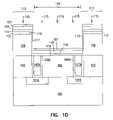
- a metallic conductor 120is deposited over the seed layer 116 in the number of trenches 110 .
- metallic conductor 120is selected from the group consisting of aluminum, copper, silver, and gold depending on the type of seed layer 116 which was deposited.
- the metallic conductor 120 , or number of first level metal lines 120are selectively formed on the copper seed layer 116 such that the number of copper metal lines 120 , or first level copper metal lines 120 are not formed on the top surface 119 of the first insulator layer 108 .
- the metallic conductor 120is deposited using a selective CVD process.
- depositing a metallic conductor 120 , or number of first level metal lines 120 , over the seed layer 116includes depositing a metallic conductor 120 using electroless plating. Electroless copper plating is used to deposit sufficient copper to fill the number of trenches 110 to the top surface 119 of the first insulator layer 108 .
- FIG. 1Gillustrates the structure after the next sequence of processing steps.
- a dual damascene processis used to define and fill a first to a second level of vias and a second level metallurgy.
- a second polymer layer 124or second layer of polyimide 124 , is deposited over the wafer surface, e.g. the metallic conductor 120 , or number of first level metal lines 120 , and the first polymer layer 108 .
- the second polymer layer 124may similarly be deposited using, for example, the process and material described in co-pending and commonly assigned application U.S. Ser.
- depositing a second polymer layer 124includes depositing a foamed second polymer layer 124 .
- the second polymer layer 124is deposited and cured, forming a 10,000 ⁇ thick second polymer layer 124 after curing.
- suitable thickness for the second polymer layer 124 , or second insulator layer/material 124may also be deposited as suited for forming a first to a second level of vias, e.g. second level vias, and a number of second level metal lines, the invention is not so limited.
- the second polymer layer 124 , or second insulator layer/material 124is patterned to define a second level of vias and a number of second level metal lines in the second insulator layer/material 124 opening to the metallic conductor 120 , or number of first level metal lines 120 .
- a second level of viasis defined in a second mask layer of photoresist 126 and then the second polymer layer 124 is etched, using any suitable process, e.g. reactive ion etching (RIE), such that a second level of via openings 128 are defined in the polyimide.
- RIEreactive ion etching
- a number of second level metal linesare also defined in a second mask layer of photoresist 126 and the second polymer layer 124 is again etched, using any suitable process, e.g. reactive ion etching (RIE), such that a second level of metal line trenches 130 are defined in the polyimide.
- RIEreactive ion etching
- a residual photoresist layer 126is left in place on the second insulator layer/material 124 in a number of regions 132 outside of the second level of metal line trenches 130 .
- a suitable plasma and/or wet cleaning processis used to remove any contaminates from the second level of via openings 128 and a second level of metal line trenches 130 , as the same will be understood by one of ordinary skill in the art upon reading this disclosure.
- the structureis now as appears in FIG. 1G .
- FIG. 1Hillustrates the structure 100 after the next sequence of processing steps.
- a second barrier/adhesion layer 134is deposited in the second level of via openings 128 and a second level of metal line trenches 130 using a low energy ion implantation.
- depositing the second barrier/adhesion layer 134includes depositing a layer of zirconium 134 having a thickness of approximately 5 to 100 ⁇ .
- depositing the second barrier/adhesion layer 134includes depositing a barrier/adhesion layer 134 of titanium and/or hafnium.
- depositing the layer of zirconium 134includes depositing a layer of zirconium 134 having a thickness of approximately 50 ⁇ . In one embodiment, this is achieved using a 10 17 ion implant of zirconium. According to the teachings of the present invention, the layer of zirconium 134 is implanted at 100 electron volts (eV) into the surface of the second level of via openings 128 and a second level of metal line trenches 130 in the second polymer layer 124 using a varying angle, as shown by arrows 125 , implant where the angle of implantation is changed from normal to the wafer surface to 15 degrees off normal.
- eVelectron volts
- FIG. 1Iillustrates the structure 100 after the next sequence of processing steps.
- a second seed layer 136is deposited on the second barrier/adhesion layer 134 using a low energy ion implantation.
- depositing the second seed layer 136 on the second barrier/adhesion layer 114includes depositing a second seed layer 136 selected from the group consisting of aluminum, copper, silver, and gold.
- depositing the second seed layer 136includes depositing a second layer of copper 136 having a thickness of approximately a 100 ⁇ . In one embodiment, this is achieved using an 8 ⁇ 10 16 ion implant of copper.
- using a low energy ion implantationincludes implanting the layer of copper 136 at 100 electron volts (eV) into the surfaces of the second level of via openings 128 and the polymer layer. Also the layer of copper 136 is implanted at an angle normal to the wafer's surface as shown by arrows 137 .
- eVelectron volts
- implanting the layer of copper 136 at an angle normal to the planarized surfaceresults in the second seed layer of copper 136 remaining on a bottom surface 138 in the second level of via openings 128 and second level of metal line trenches 130 and to a much lesser extent on the side surfaces 140 of the second level of via openings 128 and a second level of metal line trenches 130 .
- an optional layer of aluminum 141is deposited over the second copper seed layer 136 again using a low energy ion implantation of 100 electron volts (eV).
- the optional layer of aluminumis deposited to have a thickness of approximately a 50 ⁇ .
- thisis achieved using a 3 ⁇ 10 16 ion implant of aluminum normal to the wafer surface.
- the layer of aluminum 141is used to protect the second copper seed layer 136 from oxidation prior to subsequent processing steps.
- FIG. 1Jillustrates the structure after the next sequence of processing steps.
- the residual photoresist layer 126has served as a blocking layer to define the implant areas for the second barrier/adhesion layer 134 , the second seed layer 136 , and the aluminum layer 141 .
- the residual photoresist layer 126is now removed using a wet strip process, as the same will be understood by one of ordinary skill in the art upon reading this disclosure.
- removing the residual photoresist layer 126includes removing the unwanted aluminum layer 141 , the unwanted seed layer 136 , and the unwanted barrier/adhesion layer 134 from other areas of the wafer's surface, e.g. from over a number of regions 132 outside of second level of metal line trenches 130 on a top surface 142 of the second insulator layer 124 .
- the structureis now as shown in FIG. 1J .
- a second metallic conductor 144is deposited over or formed on the second seed layer 136 and within the second barrier/adhesion layer 134 in the second level of via openings 128 and the second level of metal line trenches 130 in the polymer layer.
- the second metallic conductor 144is copper, but in other embodiments of the present invention can be selected from the group consisting of aluminum, silver, and gold.
- the second metallic conductor 144 , or second core conductor 144is deposited using a selective CVD process such that the second metallic conductor 144 , or second core conductor 144 is not formed on a top surface 142 of the second insulator layer 124 .
- depositing a second metallic conductor 144 , or second core conductor 144 , over on the second seed layer 136 and within the second barrier/adhesion layer 134includes depositing a second metallic conductor 144 , or second core conductor 144 , using electroless plating.
- Electroless copper platingis used to deposit sufficient copper to fill the second level of via openings 128 and the second level of metal line trenches 130 to the top surface 142 of the second insulator layer 124 .
- the second barrier/adhesion layer 134 , the second seed layer 136 , and the second metallic conductor 144 , or second core conductor 144constitute a second number of conductive structures which includes a number of second level vias and a number of second level metal lines which are formed over and connect to a first number of conductive structures, e.g. the first level metal lines 120 .
- FIGS. 2A-2Killustrate a novel methodology for the formation of metal interconnects and/or a wiring structure in an integrated circuit according to the teachings of the present invention.
- the novel methodologyincludes the novel formation of a barrier/adhesion layer and a seed layer in an integrated circuit using a low energy ion implantation.
- the novel methodologyalso encompasses a novel method of making copper, silver, aluminum, or gold interconnect for an integrated circuit.
- FIG. 2Aillustrates a portion of an integrated circuit structure, namely an integrated circuit having a number of semiconductor devices formed in a substrate as described above in connection with FIG. 1A . That is, FIG. 2A illustrates the structure after a device structure is formed in the substrate and the contact structure to the device structure is in place. Like FIG. 1A , FIG. 2A illustrates the structure after a number of device structures, e.g. transistor 201 A and 201 B are formed in the substrate 200 . An insulator layer 202 is deposited over the number of semiconductors 201 A and 201 B. The deposition of the insulator layer 202 can include depositing a layer of Si 3 N 4 having a thickness in the range of 100 to 500 Angstroms ( ⁇ ).
- Contact holes 205 A and 205 Bare opened to the number of device structures 201 A and 201 B using a photolithography technique.
- a photolithography techniquecan be used to create contact holes 205 A and 205 B.
- a titanium silicide liner 206 A and 206 Bis placed in the contact holes 205 A and 205 B, such a through a process such as chemical vapor deposition (CVD).
- CVDchemical vapor deposition
- tungsten vias 207 A and 207 Bcan be deposited in the contact holes 205 A and 205 B.
- the tungsten vias 207 A and 207 Bcan be deposited in the contact holes using any suitable technique such as using a CVD process.
- the excess tungstenis then removed from the wafer surface by chemical mechanical planarization (CMP) or other suitable processes to form a planarized surface 209 .
- CMPchemical mechanical planarization
- a first oxide layer 208e.g. a silicon dioxide layer (SiO 2 ), is deposited over the wafer surface.
- depositing a first oxide layer 208includes depositing a fluorinated silicon oxide layer 208 .
- the first oxide layer 208may be deposited using any suitable technique, such as, for example, using a CVD process.
- depositing a first oxide layer 208 having a thickness of approximately 5000 ⁇may also be deposited as suited for forming a first level metal pattern, the invention is not so limited.
- the first oxide layer 208is patterned to define a number of trenches 210 in the first oxide layer 208 opening to a number of first level vias, e.g. tungsten vias 207 A and 207 B in planarized surface 209 .
- a first level metal pattern 210is defined in a mask layer of photoresist 212 and then the first oxide layer 208 is etched, using any suitable process, e.g. reactive ion etching (RIE), such that the first level metal pattern 210 is defined in the first oxide layer 208 .
- RIEreactive ion etching
- any desired first level metal pattern 210can be created using a photolithography technique.
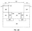
- a residual photoresist layer 212is left in place on the first oxide layer 208 in a number of region 213 outside of the number trenches 210 .
- the structureis now as appears in FIG. 2B .
- a first barrier/adhesion layer 214is deposited in the number of trenches 210 using a low energy ion implantation.
- depositing the barrier/adhesion layer 214includes depositing a layer of zirconium 214 having a thickness of approximately 5 to 100 ⁇ .
- depositing the barrier/adhesion layer 214includes depositing a barrier/adhesion layer 214 of titanium and/or hafnium.
- depositing the depositing a layer of zirconium 214includes depositing a layer of zirconium 214 having a thickness of approximately 50 ⁇ .
- the layer of zirconium 214is implanted at 100 electron volts (eV) into the surface of the trenches 210 in the first oxide layer 208 using a varying angle implant ( ⁇ ), as represented by arrows 211 , where the angle of implantation is changed from normal to the wafer surface to 15 degrees off normal.
- a varying angle implantwhere an angle of implantation ( ⁇ ) is changed from normal to the wafer's surface to approximately 15 degrees off normal deposits the barrier/adhesion layer 214 on all surfaces in the number of trenches 210 .
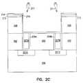
- FIG. 2CThe structure is now as appears in FIG. 2C .
- a first seed layer 216is deposited on the first barrier/adhesion layer 214 using a low energy ion implantation.
- depositing the seed layer 216 on the barrier/adhesion layer 214includes depositing a first seed layer 216 selected from the group consisting of aluminum, copper, silver, and gold.
- depositing the seed layer 216includes depositing a layer of an aluminum copper alloy 216 having a thickness of approximately 110 ⁇ .
- a layer of copper 282is then deposited on the first layer of aluminum 281 to a thickness of approximately 10 ⁇ using a low energy ion implantation of approximately 100 eV.
- a second layer of aluminum 283is then deposited on the layer of copper 282 to a thickness of approximately 50 ⁇ using a low energy ion implantation of approximately 100 eV.
- the first seed layer 216is implanted at an angle normal to the planarized surface, as shown by arrows 215 .
- implanting the first seed layer 216 at an angle normal to the planarized surfaceresults in the first seed layer 216 remaining on a bottom surface 218 in the number of trenches 210 and to a much lesser extent on the side surfaces 217 of the number of trenches 210 .
- FIG. 2Eillustrates the structure after the next sequence of processing steps.
- the residual photoresist layer 212has served as a blocking layer to define the implant areas for the barrier/adhesion layer 214 and the seed layer 216 .
- the residual photoresist layer 212is now removed using a wet strip process, as the same will be understood by one of ordinary skill in the art upon reading this disclosure.
- removing the residual photoresist layer 212includes removing the unwanted seed layer 216 and the unwanted barrier/adhesion layer 214 from other areas of the wafer's surface, e.g. from over a number of regions 213 outside of the trenches 210 on a top surface 219 of the first insulator layer 208 .
- the structureis now as shown in FIG. 2E .
- a metallic conductor 220is deposited over the first seed layer 216 and within the first barrier/adhesion layer 214 in the number of trenches 210 .
- the metallic conductor 220is aluminum, but in other embodiments of the present invention the metallic conductor 220 , or number of first level metal lines 220 , is selected from the group consisting of copper, silver, and gold depending on the type of seed layer 216 which was deposited.
- the metallic conductor 220 , or number of first level metal lines 220is deposited using a selective CVD process.
- depositing a metallic conductor 220 , or number of first level metal lines 220 , over the seed layer 216includes depositing a metallic conductor 220 using electroless plating.
- the number of first level aluminum metal lines 220is deposited to fill the number of trenches 210 to the top surface 219 of the first oxide layer 208 .
- the first level aluminum metal lines 220 , the first seed layer 216 , and the first barrier/adhesion layer 214 in the number of trenches 210constitute a first number of conductive structures.
- the copper composition of the first seed layer 216can be adjusted to give the appropriate percentage of copper in the completed first number of conductive structures.
- the layer thicknesses of the aluminum copper sandwichwas designed to give a 0.7 weight percent of copper in the first number of conductive structures.
- FIG. 2Gillustrates the structure after the next sequence of processing steps.
- a dual damascene processis used to define and fill a first to a second level of vias and a second level metallurgy.
- a second oxide layer 224is deposited over the wafer surface, e.g. the metallic conductor 220 , or number of first level metal lines 220 , and the first oxide layer 208 .
- depositing a second oxide layer 224includes depositing a second fluorinated silicon oxide layer 224 .
- the second oxide layer 224is formed to have a thickness of approximately 10,000 ⁇ .
- suitable thickness for the second oxide layer 224may also be deposited as suited for forming a first to a second level of vias, e.g. second level vias, and a number of second level metal lines, the invention is not so limited.
- the second oxide layer 224is patterned to define a second level of vias and a number of second level metal lines in the second oxide layer 224 opening to the metallic conductor 220 , or number of first level metal lines 220 .
- a second level of viasis defined in a second mask layer of photoresist 226 and then the second oxide layer 224 is etched, using any suitable process, e.g. reactive ion etching (RIE), such that a second level of via openings 228 are defined in the polyimide.
- RIEreactive ion etching
- a number of second level metal linesare also defined in a second mask layer of photoresist 226 and the second oxide layer 224 is again etched, using any suitable process, e.g. reactive ion etching (RIE), such that a second level of metal line trenches 230 are defined in the second oxide layer 224 .
- RIEreactive ion etching
- a photoresist layer 226can be mask, exposed, and developed using a dual damascene process to pattern a second level of via openings 228 and a second level of metal line trenches 230 in the second oxide layer 224 .
- a residual photoresist layer 226is left in place on the second oxide layer 224 in a number of regions 232 outside of the second level of metal line trenches 230 .
- a suitable plasma and/or wet cleaning processis used to remove any contaminates from the second level of via openings 228 and a second level of metal line trenches 230 , as the same will be understood by one of ordinary skill in the art upon reading this disclosure.
- the structureis now as appears in FIG. 2G .
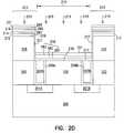
- FIG. 2Hillustrates the structure after the next sequence of processing steps.
- a second barrier/adhesion layer 234is deposited in the second level of via openings 228 and a second level of metal line trenches 230 using a low energy ion implantation.
- depositing the second barrier/adhesion layer 234includes depositing a layer of zirconium 234 having a thickness of approximately 5 to 100 ⁇ .
- depositing the second barrier/adhesion layer 234includes depositing a barrier/adhesion layer 234 of titanium and/or hafnium.
- depositing the layer of zirconium 234includes depositing a layer of zirconium 234 having a thickness of approximately 50 ⁇ . In one embodiment, this is achieved using a 10 17 ion implant of zirconium (that is 10 17 ions per square centimeter). According to the teachings of the present invention, the layer of zirconium 234 is implanted at 100 electron volts (eV) into the surface of the second level of via openings 228 and a second level of metal line trenches 230 in the second polymer layer 224 using a varying angle implant ( ⁇ ), as shown by arrows 225 where the angle of implantation is changed from normal to the wafer surface to 15 degrees off normal.
- eVelectron volts
- ⁇varying angle implant
- FIG. 2Iillustrates the structure after the next sequence of processing steps.
- a second seed layer 236is deposited on the second barrier/adhesion layer 234 using a low energy ion implantation.
- depositing the second seed layer 236 on the second barrier/adhesion layer 214includes depositing a second seed layer 236 selected from the group consisting of aluminum, copper, silver, and gold.
- depositing the seed layer 216includes depositing a layer of an aluminum copper alloy 216 having a thickness of approximately 110 ⁇ .
- first layer of aluminum 284on the barrier/adhesion layer 214 to a thickness of approximately 50 ⁇ using a low energy ion implantation of approximately 100 electron volts (eV).
- a layer of copper 285is then deposited on the first layer of aluminum 284 to a thickness of approximately 10 ⁇ using a low energy ion implantation of approximately 100 eV.
- a second layer of aluminum 286is then deposited on the layer of copper 285 to a thickness of approximately 50 ⁇ using a low energy ion implantation of approximately 100 eV.
- the first seed layer 216is implanted at an angle normal to the wafer's surface as shown by arrows 237 .
- implanting the layer of copper 236 at an angle normal to the planarized surfaceresults in the second seed layer of copper 236 remaining on a bottom surface 238 in the second level of via openings 228 and to a much lesser extent on the side surfaces 240 of the second level of via openings 228 and a second level of metal line trenches 230 .
- FIG. 2Jillustrates the structure following the next sequence of process steps.
- the residual photoresist layer 226has served as a blocking layer to define the implant areas for the second barrier/adhesion layer 234 and the second seed layer 236 .
- the residual photoresist layer 226is now removed using a wet strip process, as the same will be understood by one of ordinary skill in the art upon reading this disclosure.
- removing the residual photoresist layer 226includes removing the unwanted barrier/adhesion layer 234 and the unwanted second seed layer 236 , from other areas of the wafer's surface, e.g. from over a number of regions 232 outside of second level of metal line trenches 230 on a top surface 242 of the second oxide layer 224 .
- the structureis now as shown in FIG. 2J .
- a second metallic conductor 244is deposited over or formed on the second seed layer 236 and within the second barrier/adhesion layer 234 in the second level of via openings 228 and the second level of metal line trenches 230 in the polymer layer.
- the second metallic conductor 244 , or second core conductor 244is aluminum, but in other embodiments of the present invention the second metallic conductor 244 , or second core conductor 244 , can be selected from the group consisting of copper, silver, and gold.
- the second metallic conductor 244 , or second core conductor 244is deposited using a selective CVD process.
- depositing a second metallic conductor 244 , or second core conductor 244 , over on the second seed layer 236 and within the second barrier/adhesion layer 234includes depositing a second metallic conductor 244 , or second core conductor 244 , using electroless plating.
- the second aluminum conductor 244 , or second core conductor 244is deposited to fill the second level of via openings 228 and the second level of metal line trenches 230 to the top surface 242 of the second insulator layer 224 .
- the second barrier/adhesion layer 234 , the second seed layer 236 , and the second metallic conductor 244 , or second core conductor 244constitute a second number of conductive structures which includes a number of second level vias and a number of second level metal lines which are formed over and connect to a first number of conductive structures, e.g. the first level of vias 207 A and 207 B.
- FIGS. 3A-3Killustrate a novel methodology for the formation of metal interconnects and/or a wiring structure in an integrated circuit according to the teachings of the present invention.
- the novel methodologyincludes the novel formation of a barrier/adhesion layer and a seed layer in an integrated circuit using a low energy ion implantation.
- the novel methodologyalso encompasses a novel method of making copper, silver, aluminum, or gold interconnect for an integrated circuit.
- FIG. 3Aillustrates a portion of an integrated circuit structure, namely an integrated circuit having a number of semiconductor devices formed in a substrate.
- FIG. 3illustrates the structure after a device structure is formed in the substrate and the contact structure to the device structure is in place.
- a number of semiconductor structurese.g. transistors
- FIG. 3Aillustrates the structure after a number of device structures, e.g. transistor 301 A and 301 B are formed in the substrate 300 .
- An insulator layer 302is deposited over the number of semiconductors 301 A and 301 B.
- the deposition of the insulator layer 302can include depositing a layer of Si 3 N 4 having a thickness in the range of 100 to 500 Angstroms ( ⁇ ). This insulator layer will also serve as an additional barrier to impurities coming from subsequent processing steps.
- Contact holes 305 A and 305 Bare opened to the number of device structures 301 A and 301 B using a photolithography technique.
- a photolithography techniqueOne of ordinary skill in the are will understand, upon reading this disclosure, the manner in which a photolithography technique can be used to create contact holes 305 A and 305 B.
- a titanium silicide liner 306 A and 306 Bis placed in the contact holes 305 A and 305 B, such a through a process such as chemical vapor deposition (CVD).
- CVDchemical vapor deposition
- tungsten vias 306 A and 306 Bcan be deposited in the contact holes 305 A and 305 B.
- the tungsten vias 307 A and 307 Bcan be deposited in the contact holes using any suitable technique such as using a CVD process.
- the excess tungstenis then removed from the wafer surface by chemical mechanical planarization (CMP) or other suitable processes to form a planarized surface 309 .
- CMPchemical mechanical planarization
- a first polymer layer 308is deposited over the wafer surface.
- the first oxide layer 308may be deposited using any suitable technique such as, for example, a CVD process.
- depositing a first oxide layer 308includes depositing a fluorinated silicon oxide layer 308 .
- the first oxide layer 308is deposited to have a thickness of approximately 5000 ⁇ . As one of ordinary skill in the art will understand, upon reading this disclosure, other suitable thickness for the first oxide layer 308 may also be deposited as suited for forming a first level metal pattern, the invention is not so limited.
- the first oxide layer 308is patterned to define a number of trenches 310 in the first oxide layer 308 opening to a number of first level vias, e.g. tungsten vias 307 A and 307 B in planarized surface 309 .
- a first level metal pattern 310is defined in a mask layer of photoresist 312 and then the first oxide layer 308 is etched, using any suitable process, e.g. reactive ion etching (RIE), such that the first level metal pattern 310 is defined in the first oxide layer 308 .
- RIEreactive ion etching
- a residual photoresist layer 312is left in place on the first oxide layer 308 in a number of region 313 outside of the number trenches 310 .
- the structureis now as appears in FIG. 3B .
- a first barrier/adhesion layer 314is deposited in the number of trenches 310 using a low energy ion implantation.
- depositing the barrier/adhesion layer 314includes depositing a tantalum nitride layer 314 having a thickness of approximately 5 to 100 ⁇ .
- depositing the barrier/adhesion layer 314includes depositing a barrier/adhesion layer 314 of tantalum and/or CuTi.
- depositing the tantalum nitride layer 314includes first depositing a layer of tantalum 381 to have a thickness of approximately 100 ⁇ using a low energy ion implantation of approximately 100 electron volts (eV) at a varying angle implant ( ⁇ ), e.g. the angle of implantation ( ⁇ ) is changed from normal to the planarized surface 309 to approximately 15 degrees off normal as shown by arrows 311 . In one embodiment, this is achieved using a 10 17 ion implant of tantalum.
- a layer of nitrogen 382is implanted at 700 electron volts (eV) into the layer of tantalum 381 .
- thisis achieved using an 8 ⁇ 10 16 ion implant of nitrogen.
- an angle of implantationis changed from normal to the planarized surface 309 to approximately 15 degrees off normal deposits the barrier/adhesion layer 314 on all surfaces in the number of trenches 310 .
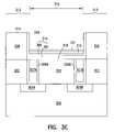
- the structureis now as appears in FIG. 3C .
- a first seed layer 316is deposited on the first barrier/adhesion layer 314 using a low energy ion implantation.
- depositing the seed layer 316 on the barrier/adhesion layer 314includes depositing a seed layer 316 selected from the group consisting of aluminum, copper, silver, and gold.
- depositing the seed layer 316includes depositing a layer of copper 316 having a thickness of approximately 50 ⁇ . This can be achieved using an 8 ⁇ 10 16 ion implant of copper.
- using a low energy ion implantationincludes implanting the layer of copper 316 at 100 electron volts (eV) into the first barrier/adhesion layer 314 . Also the layer of copper 316 is implanted at an angle normal to the planarized surface 309 as shown by arrows 315 . As one of ordinary skill in the art will understand upon reading this disclosure, implanting the layer of copper 316 at an angle normal to the planarized surface results in the seed layer of copper 316 remaining on a bottom surface 318 in the number of trenches 310 and to a much lesser extent on the side surfaces 320 of the number of trenches 310 .
- eVelectron volts
- an optional layer of aluminum 321is deposited over the copper seed layer 316 again using a low energy ion implantation of 100 electron volts (eV).
- the optional layer of aluminum 321is deposited to have a thickness of approximately a 50 ⁇ . This can be achieved using a 3 ⁇ 10 16 ion implant of aluminum normal to the wafer surface.
- the layer of aluminum 321is used to protect the copper seed layer 316 from oxidation prior to subsequent processing steps. The structure is now as appears in FIG. 3D .
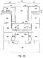
- FIG. 3Eillustrates the structure after the next sequence of processing steps.
- the residual photoresist layer 312has served as a blocking layer to define the implant areas for the barrier/adhesion layer 314 , the seed layer 316 , and the layer of aluminum 321 .
- the residual photoresist layer 312is now removed using a wet strip process, as the same will be understood by one of ordinary skill in the art upon reading this disclosure.
- removing the residual photoresist layer 312includes removing the unwanted aluminum layer 321 , the unwanted seed layer 316 , and the unwanted barrier/adhesion layer 314 from other areas of the wafer's surface, e.g. from over a number of regions outside of the trenches 310 on a top surface 319 of the first insulator layer 308 .
- the structureis now as shown in FIG. 3E .
- a metallic conductor 320is deposited over the seed layer 316 in the number of trenches 310 .
- the metallic conductor 320 , or number of first level metal lines 320is copper.
- the metallic conductor 320 , or number of first level metal lines 320is deposited using a selective CVD process.
- depositing a metallic conductor 320 , or number of first level metal lines 320 , over the seed layer 316includes depositing a metallic conductor 320 using electroless plating.
- Electroless copper platingis used to deposit sufficient copper to fill the number of trenches 310 to a level approximately 100 ⁇ below the top surface 319 of the first oxide layer 308 .
- a second layer of tantalum nitride 323is deposited to a thickness of approximately 100 ⁇ on the copper metallic conductor 320 , or number of first level copper lines 320 .
- a chemical mechanical planarization (CMP) cleanup processis then used to remove the tantalum nitride from the top surface 319 of the first oxide layer 308 .
- FIG. 3Gillustrates the structure after the next sequence of processing steps.
- a dual damascene processis used to define and fill a first to a second level of vias and a second level metallurgy.
- a second oxide layer 324is deposited over the wafer surface, e.g. the metallic conductor 320 , or number of first level metal lines 320 , and the first oxide layer 308 .
- the second oxide layer 324is again deposited using any suitable technique.
- depositing a second oxide layer 324includes depositing a fluorinated silicon oxide layer 324 .
- the second oxide layer 324is deposited to have a thickness of approximately 10,000 ⁇ . As one of ordinary skill in the art will understand, upon reading this disclosure, other suitable thickness for the second oxide layer 324 may also be deposited as suited for forming a first to a second level of vias, e.g. second level vias, and a number of second level metal lines, the invention is not so limited.
- the second oxide layer 324is patterned to define a second level of vias and a number of second level metal lines in the second oxide layer 324 opening to the metallic conductor 320 , or number of first level metal lines 320 .
- a second level of viasis defined in a second mask layer of photoresist 326 and then the second oxide layer 324 is etched, using any suitable process, e.g. reactive ion etching (RIE), such that a second level of via openings 328 are defined in the second oxide layer 324 .
- RIEreactive ion etching
- a number of second level metal linesare also defined in a second mask layer of photoresist 326 and the second oxide layer 324 is again etched, using any suitable process, e.g. reactive ion etching (RIE), such that a second level of metal line trenches 330 are defined in the oxide.
- a photoresist layer 326can be mask, exposed, and developed using a dual damascene process to pattern a second level of via openings 328 and a second level of metal line trenches 330 in the second oxide layer 324 .
- a residual photoresist layer 326is left in place on the second oxide layer 324 in a number of regions 332 outside of the second level of metal line trenches 330 .
- a suitable plasma and/or wet cleaning processis used to remove any contaminates from the second level of via openings 328 and a second level of metal line trenches 330 , as the same will be understood by one of ordinary skill in the art upon reading this disclosure.
- the structureis now as appears in FIG. 3G .
- FIG. 3Hillustrates the structure after the next sequence of processing steps.
- a second barrier/adhesion layer 334is deposited in the second level of via openings 328 and a second level of metal line trenches 330 using a low energy ion implantation.
- depositing the second barrier/adhesion layer 334includes depositing a tantalum nitride layer 334 having a thickness of approximately 5 to 100 ⁇ .
- depositing the second barrier/adhesion layer 334includes depositing a second barrier/adhesion layer 334 of tantalum and/or CuTi.
- depositing the tantalum nitride layer 334includes first depositing a layer of tantalum 383 to have a thickness of approximately 100 ⁇ using a low energy ion implantation of approximately 100 electron volts (eV) at a varying angle implant ( ⁇ ), e.g. the angle of implantation ( ⁇ ) is changed from normal to the wafer's surface to approximately 15 degrees off normal as shown by arrows 325 . In one embodiment, this is achieved using a 10 17 ion implant of tantalum.
- a layer of nitrogen 384is implanted at 700 electron volts (eV) into the layer of tantalum 383 .
- thisis achieved using an 8 ⁇ 10 16 ion implant of nitrogen.
- ⁇varying angle implant
- FIG. 3Iillustrates the structure after the next sequence of processing steps.
- a second seed layer 336is deposited on the second barrier/adhesion layer 334 using a low energy ion implantation.
- depositing the second seed layer 336 on the second barrier/adhesion layer 314includes depositing a second seed layer 336 selected from the group consisting of aluminum, copper, silver, and gold.
- depositing the second seed layer 336includes depositing a second layer of copper 336 having a thickness of approximately 50 ⁇ . In one embodiment, this is achieved using an 8 ⁇ 10 16 ion implant of copper.
- using a low energy ion implantationincludes implanting the layer of copper 336 at 100 electron volts (eV) into the surfaces of the second level of via openings 328 and the second level of metal line trenches 330 in the polymer layer. Also the layer of copper 336 is implanted at an angle normal to the wafer's surface as shown by arrows 337 .
- eVelectron volts
- implanting the layer of copper 336 at an angle normal to the wafer's surfaceresults in the second seed layer of copper 336 remaining on a bottom surface 338 in the second level of via openings 328 and to a much lesser extent on the side surfaces 340 of the second level of via openings 328 and a second level of metal line trenches 330 .
- an optional layer of aluminum 341is deposited over the second copper seed layer 336 again using a low energy ion implantation of 100 electron volts (eV).
- the optional layer of aluminumis deposited to have a thickness of approximately a 50 ⁇ . In one embodiment, this is achieved using a 3 ⁇ 10 16 ion implant of aluminum normal to the wafer surface.
- the layer of aluminum 341is used to protect the second copper seed layer 336 from oxidation prior to subsequent processing steps. The structure is now as shown in FIG. 3I .
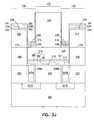
- FIG. 3Jillustrates the structure after the next sequence of processing steps.
- the residual photoresist layer 326has served as a blocking layer to define the implant areas for the second barrier/adhesion layer 334 , the second seed layer 336 , and the aluminum layer 341 .
- the residual photoresist layer 326is now removed using a wet strip process, as the same will be understood by one of ordinary skill in the art upon reading this disclosure.
- removing the residual photoresist layer 326includes removing the unwanted aluminum layer 341 , the unwanted seed layer 336 , and the unwanted barrier/adhesion layer 334 from other areas of the wafer's surface, e.g. from over a number of regions 332 outside of second level of metal line trenches 330 on a top surface 342 of the second insulator layer 324 .
- the structureis now as shown in FIG. 3J .
- a second metallic conductor 344is deposited over or formed on the second seed layer 336 and within the second barrier/adhesion layer 334 in the second level of via openings 328 and the second level of metal line trenches 330 in the polymer layer.
- the second metallic conductor 344 , or second core conductor 344is copper, but in other embodiments of the present invention the second metallic conductor 344 , or second core conductor 344 , can be selected from the group consisting of aluminum, silver, and gold.
- the second metallic conductor 344 , or second core conductor 344is deposited using a selective CVD process.
- depositing a second metallic conductor 344 , or second core conductor 344 , over on the second seed layer 336 and within the second barrier/adhesion layer 334includes depositing a second metallic conductor 344 , or second core conductor 344 , using electroless plating. Electroless copper plating is used to deposit sufficient copper to fill the second level of via openings 328 and the second level of metal line trenches 330 to level approximately 100 ⁇ below the top surface 342 of the second insulator layer 324 . At this point, a second layer of tantalum nitride 346 is deposited to a thickness of approximately 100 ⁇ on the second metallic conductor 344 , or second core conductor 344 .
- the second barrier/adhesion layer 334 , the second seed layer 336 , and the second metallic conductor 344 , or second core conductor 344constitute a second number of conductive structures which includes a number of second level vias and a number of second level metal lines which are formed over and connect to a first number of conductive structures, e.g. the metallic conductor 320 , or number of first level metal lines 320 .
- FIGS. 4A-4Lillustrate a novel methodology for the formation of metal interconnects and/or a wiring structure in an integrated circuit according to the teachings of the present invention.
- the novel methodologyincludes the novel formation of a barrier/adhesion layer and a seed layer in an integrated circuit using a low energy ion implantation.
- the novel methodologyalso encompasses a novel method of making copper, silver, aluminum, or gold interconnect for an integrated circuit.
- FIG. 4Aillustrates a portion of an integrated circuit structure, namely an integrated circuit having a number of semiconductor devices formed in a substrate.
- FIG. 4Aillustrates the structure after a device structure is formed in the substrate and the contact structure to the device structure is in place.
- a number of semiconductor structurese.g. transistors
- FIG. 4Aillustrates the structure after a number of device structures, e.g. transistor 401 A and 401 B are formed in the substrate 400 .
- An insulator layer 402is deposited over the number of semiconductors 401 A and 401 B.
- the deposition of the insulator layer 402can include depositing a layer of Si 3 N 4 having a thickness in the range of 100 to 500 Angstroms ( ⁇ ). This insulator layer will also serve as an additional barrier to impurities coming from subsequent processing steps.
- Contact holes 405 A and 405 Bare opened to the number of device structures 401 A and 401 B using a photolithography technique.
- a photolithography techniqueOne of ordinary skill in the are will understand, upon reading this disclosure, the manner in which a photolithography technique can be used to create contact holes 405 A and 405 B.
- a titanium silicide liner 406 A and 406 Bis placed in the contact holes 405 A and 405 B, such a through a process such as chemical vapor deposition (CVD).
- CVDchemical vapor deposition
- tungsten vias 407 A and 407 Bcan be deposited in the contact holes 405 A and 405 B.
- the tungsten vias 407 A and 407 Bcan be deposited in the contact holes using any suitable technique such as using a CVD process.
- the excess tungstenis then removed from the wafer surface by chemical mechanical planarization (CMP) or other suitable processes to form a planarized surface 409 .
- CMPchemical mechanical planarization
- a first polymer layer 408is deposited over the wafer surface.
- the first polymer layer 408may be deposited using, for example, the process and material described in co-pending and commonly assigned application U.S. Ser. No. 09/128,859, entitled “Copper Metallurgy in Integrated Circuits,” which is hereby incorporated by reference.
- depositing a first polymer layer 408includes depositing a foamed polymer layer 408 .
- the first layer of polyimide 408is deposited and cured, forming a 5000 ⁇ thick layer of polymer 408 after curing.
- first layer of polyimide 408may also be deposited as suited for forming a first level metal pattern, the invention is not so limited.
- the first layer of polyimide 408 , or first insulator layer/material 408is patterned to define a number of trenches 410 in the first insulator layer 408 opening to a number of first level vias, e.g. tungsten vias 407 A and 407 B in planarized surface 409 .
- a first level metal pattern 410is defined in a mask layer of photoresist 412 and then the first layer of polyimide 408 is etched, using any suitable process, e.g. reactive ion etching (RIE), such that the first level metal pattern 410 is defined in the polyimide.
- RIEreactive ion etching
- a residual photoresist layer 412is left in place on the first insulator layer 408 in a number of region 413 outside of the number trenches 410 .
- the structureis now as appears in FIG. 4B .
- a first barrier/adhesion layer 414is deposited in the number of trenches 410 using a low energy ion implantation.
- depositing the barrier/adhesion layer 414includes depositing a layer of zirconium 414 having a thickness of approximately 5 to 100 ⁇ .
- depositing the barrier/adhesion layer 414includes depositing a barrier/adhesion layer 414 of titanium and/or hafnium.
- depositing the depositing a layer of zirconium 414includes depositing a layer of zirconium 414 having a thickness of approximately 15 ⁇ .
- the layer of zirconium 414is implanted at 100 electron volts (eV) into the surface of the trenches 410 in the polymer layer 408 using an angle of implant normal to the wafer's surface as shown by arrows 411 .
- eVelectron volts
- a first seed layer 416is deposited on the first barrier/adhesion layer 414 using a low energy ion implantation.
- depositing the seed layer 416 on the barrier/adhesion layer 414includes depositing a seed layer 416 selected from the group consisting of aluminum, copper, silver, and gold.
- depositing the seed layer 416includes depositing a layer of copper 416 having a thickness of approximately a 50 ⁇ . This can be achieved using an 8 ⁇ 10 16 ion implant of copper.
- using a low energy ion implantationincludes implanting the layer of copper 416 at 100 electron volts (eV) into the surface of the trenches 410 in the polymer layer. Also the layer of copper 416 is implanted at an angle normal to the wafer's surface as shown by arrows 415 . As one of ordinary skill in the art will understand upon reading this disclosure, implanting the layer of copper 416 at an angle normal to the wafer's surface results in the seed layer of copper 416 remaining on a bottom surface 418 in the number of trenches 410 and to a much lesser extent on the side surfaces 420 of the number of trenches 410 .
- eVelectron volts
- an optional layer of aluminum 421is deposited over the copper seed layer 416 again using a low energy ion implantation of 100 electron volts (eV).
- the optional layer of aluminum 421is deposited to have a thickness of approximately a 50 ⁇ . This can be achieved using a 3 ⁇ 10 16 ion implant of aluminum normal to the wafer surface as shown by arrows 415 .
- the layer of aluminum 421is used to protect the copper seed layer 416 from oxidation prior to subsequent processing steps. The structure is now as appears in FIG. 4D .
- FIG. 4Eillustrates the structure after the next sequence of processing steps.
- the residual photoresist layer 412has served as a blocking layer to define the implant areas for the barrier/adhesion layer 414 , the seed layer 416 , and the layer of aluminum 421 .
- the residual photoresist layer 412is now removed using a wet strip process, as the same will be understood by one of ordinary skill in the art upon reading this disclosure.
- removing the residual photoresist layer 412includes removing the unwanted aluminum layer 421 , the unwanted seed layer 416 , and the unwanted barrier/adhesion layer 414 from other areas of the wafer's surface, e.g. from over a number of regions 413 outside of the trenches 410 on a top surface 419 of the first insulator layer 408 .
- the structureis now as shown in FIG. 4E .
- a metallic conductor 420is deposited over the seed layer 416 in the number of trenches 410 .
- the metallic conductor 420is selected from the group consisting of aluminum, copper, silver, and gold depending on the type of seed layer 416 which was deposited.
- a number of copper metal lines 420 , or first level copper metal lines 420are selectively formed on the copper seed layer 416 .
- the metallic conductor 420 , or number of first level metal lines 420is deposited using a selective CVD process.
- depositing a metallic conductor 420 , or number of first level metal lines 420 , over the seed layer 416includes depositing a metallic conductor 420 using electroless plating. Electroless copper plating is used to deposit sufficient copper to fill the number of trenches 410 to the top surface 419 of the first insulator layer 408 .
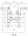
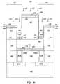
- FIG. 4Gillustrates the structure after the next sequence of processing steps.
- a dual damascene processis used to define and fill a first to a second level of vias and a second level metallurgy.
- a second polymer layer 424or second layer of polyimide 424 , is deposited over the wafer surface, e.g. the metallic conductor 420 , or number of first level metal lines 420 , and the first polymer layer 408 .
- the second polymer layer 424may similarly be deposited using, for example, the process and material described in co-pending and commonly assigned application U.S.
- depositing a second polymer layer 424includes depositing a foamed second polymer layer 424 .
- the second polymer layer 424is deposited and cured, forming a 10,000 ⁇ thick second polymer layer 424 after curing.
- suitable thickness for the second polymer layer 424 , or second insulator layer/material 424may also be deposited as suited for forming a first to a second level of vias, e.g. second level vias, and a number of second level metal lines, the invention is not so limited.
- the second polymer layer 424 , or second insulator layer/material 424is patterned to define a second level of vias and a number of second level metal lines in the second insulator layer/material 424 opening to the metallic conductor 420 , or number of first level metal lines 420 .
- a second level of viasis defined in a second mask layer of photoresist 426 and then the second polymer layer 424 is etched, using any suitable process, e.g. reactive ion etching (RIE), such that a second level of via openings 428 are defined in the polyimide.
- RIEreactive ion etching
- a number of second level metal linesare also defined in a second mask layer of photoresist 426 and the second polymer layer 424 is again etched, using any suitable process, e.g. reactive ion etching (RIE), such that a second level of metal line trenches 430 are defined in the polyimide.
- RIEreactive ion etching
- a residual photoresist layer 426is left in place on the second insulator layer/material 424 in a number of regions 432 outside of the second level of metal line trenches 430 .
- a suitable plasma and/or wet cleaning processis used to remove any contaminates from the second level of via openings 428 and a second level of metal line trenches 430 , as the same will be understood by one of ordinary skill in the art upon reading this disclosure.
- the structureis now as appears in FIG. 4G .
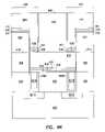
- FIG. 4Hillustrates the structure after the next sequence of processing steps.
- a second barrier/adhesion layer 434is deposited in the second level of via openings 428 and a second level of metal line trenches 430 using a low energy ion implantation.
- depositing the second barrier/adhesion layer 434includes depositing a layer of zirconium 434 having a thickness of approximately 5 to 100 ⁇ .
- depositing the second barrier/adhesion layer 434includes depositing a barrier/adhesion layer 434 of titanium and/or hafnium.
- depositing the layer of zirconium 434includes depositing a layer of zirconium 434 having a thickness of approximately 15 ⁇ . In one embodiment, this is achieved using a 10 17 ion implant of zirconium. According to the teachings of the present invention, the layer of zirconium 434 is implanted at 100 electron volts (eV) into the surface of the second level of via openings 428 and a second level of metal line trenches 430 in the second polymer layer 424 using an implant angle normal to the wafer's surface as shown by arrows 425 . The structure is now as appears in FIG. 4H .
- eVelectron volts
- FIG. 4Iillustrates the structure after the next sequence of processing steps.
- a second seed layer 436is deposited on the second barrier/adhesion layer 434 using a low energy ion implantation.
- depositing the second seed layer 436 on the second barrier/adhesion layer 414includes depositing a second seed layer 436 selected from the group consisting of aluminum, copper, silver, and gold.
- depositing the second seed layer 436includes depositing a second layer of copper 436 having a thickness of approximately a 50 ⁇ . In one embodiment, this is achieved using an 8 ⁇ 10 16 ion implant of copper.
- using a low energy ion implantationincludes implanting the layer of copper 436 at 100 electron volts (eV) into the second level of via openings 428 and the second level of metal line trenches 430 in the polymer layer. Also the layer of copper 436 is implanted at an angle normal to the wafer's surface as shown by arrows 437 .
- eVelectron volts
- implanting the layer of copper 436 at an angle normal to the wafer's surfaceresults in the second seed layer of copper 436 remaining on a bottom surface 438 in the second level of via openings 428 and to a much lesser extent on the side surfaces 440 of the second level of via openings 428 and a second level of metal line trenches 430 .
- an optional layer of aluminum 441is deposited over the second copper seed layer 436 again using a low energy ion implantation of 100 electron volts (eV).
- the optional layer of aluminumis deposited to have a thickness of approximately a 50 ⁇ . In one embodiment, this is achieved using a 3 ⁇ 10 16 ion implant of aluminum normal to the wafer surface.
- the layer of aluminum 441is used to protect the second copper seed layer 436 from oxidation prior to subsequent processing steps. The structure is now as appears in FIG. 4I .
- FIG. 4Jillustrates the structure after the next sequence of processing steps.
- the residual photoresist layer 426has served as a blocking layer to define the implant areas for the second barrier/adhesion layer 434 , the second seed layer 436 , and the aluminum layer 441 .
- the residual photoresist layer 426is now removed using a wet strip process, as the same will be understood by one of ordinary skill in the art upon reading this disclosure.
- removing the residual photoresist layer 426includes removing the unwanted aluminum layer 441 , the unwanted seed layer 436 , and the unwanted barrier/adhesion layer 434 from other areas of the wafer's surface, e.g. from over a number of regions 432 outside of second level of metal line trenches 430 on a top surface 442 of the second insulator layer 424 .
- the structureis now as shown in FIG. 4J .
- a second metallic conductor 444is deposited over or formed on the second seed layer 436 and within the second barrier/adhesion layer 434 in the second level of via openings 428 and the second level of metal line trenches 430 in the polymer layer.
- the second metallic conductor 444 , or second core conductor 444is copper, but in other embodiments of the present invention the second metallic conductor 444 , or second core conductor 444 , can be selected from the group consisting of aluminum, silver, and gold.
- the second metallic conductor 444 , or second core conductor 444is deposited using a selective CVD process.
- depositing a second metallic conductor 444 , or second core conductor 444 , over on the second seed layer 436 and within the second barrier/adhesion layer 434includes depositing a second metallic conductor 444 , or second core conductor 444 , using electroless plating. Electroless copper plating is used to deposit sufficient copper to fill the second level of via openings 428 and the second level of metal line trenches 430 to the top surface 442 of the second insulator layer 424 .
- the second barrier/adhesion layer 434 , the second seed layer 436 , and the second metallic conductor 444 , or second core conductor 444constitute a second number of conductive structures which includes a number of second level vias and a number of second level metal lines which are formed over and connect to a first number of conductive structures, e.g. the metallic conductor 420 , or number of first level metal lines 420 .
- FIG. 4Lillustrates the structure following the final sequence of processing steps.
- the entire polymer structuree.g. first polymer layer 408 and second polymer layer 424 , are removed using an O 2 plasma etch.
- the structureis now as appears in FIG. 4L .
- FIG. 5is an illustration of an embodiment of an integrated circuit formed according to the teachings of the present invention.
- the integrated circuitincludes a metal layer in an integrated circuit.
- the metal layer FIG. 5is an illustration of an embodiment of an integrated circuit 503 formed according to the teachings of the present invention.
- the integrated circuit 503includes a metal layer in an integrated circuit.
- the metal layerincludes a number of first level vias 507 A and 507 B connecting to a number of silicon devices 501 A and 501 B in a substrate 500 .
- a number of first level metal lines 520are formed above and connect to the number of first level vias 507 A and 507 B.
- a barrier/adhesion layer 514 having a thickness in the range of 5 to 150 Angstromsis formed on the number of first level vias 507 A and 507 B.
- a seed layer 516 having a thickness in the range of 5 to 150 Angstromsis formed at least between a portion of the barrier/adhesion layer 514 and the number of first level metal lines 520 .
- the barrier adhesion layer 514 having a thickness in the range of 5 to 150 Angstromsincludes a barrier/adhesion layer selected from the group consisting of titanium, zirconium, and hafnium.
- the number of first level vias 507 A and 507 B connecting to a number of silicon devices 501 A and 501 B in substrate 500are surrounded by an insulator layer 502 .
- the number of first level metal linesis selected from the group consisting of Aluminum, Copper, Silver, and Gold.
- the integrated circuit 503comprises a portion of an integrated memory circuit 503 .
- the number of silicon devices 501 A and 501 Bincludes one or more transistors 501 A and 501 B in the substrate 500 .
- any one of the embodiments as shown in FIGS. 1K , 2 K, 3 K, and/or 4 Lcan comprise a portion of an integrated circuit according to the teachings of the present invention.
- FIG. 6illustrates an embodiment of a system 600 including a portion of an integrated circuit formed according to any of the embodiments described in the present application.
- this system 600includes a processor 610 and an integrated circuit, or integrated memory circuit 630 coupled to the processor 610 .
- the processor 610can be coupled to the integrated memory circuit 630 via any suitable bus, as the same are known and understood by one of ordinary skill in the art.
- the processor 610 and integrated circuit 630are located on a single wafer or die.
- at least a portion of the integrated circuit 630includes a portion of an integrated circuit 603 as disclosed in the various embodiments provided herein.
- the structures and methodsinclude a diffusion barrier and a seed layer in an integrated circuit both formed using a low energy ion implantation followed by a selective deposition of metal lines for the integrated circuit.
- the selective deposition of the metal linesavoids the need for multiple chemical mechanical planarization (CMP) steps.
- CMPchemical mechanical planarization
- the low energy ion implantation of the present inventionallows for the distinct placement of both the diffusion barrier and the seed layer.
- a residual resistcan be used to remove the diffusion barrier and the seed layer from unwanted areas on a wafer surface.
- the structures formed by the described novel processesaccommodate aluminum, copper, gold, and silver metal interconnects.
Landscapes
- Engineering & Computer Science (AREA)
- Physics & Mathematics (AREA)
- Condensed Matter Physics & Semiconductors (AREA)
- General Physics & Mathematics (AREA)
- Manufacturing & Machinery (AREA)
- Computer Hardware Design (AREA)
- Microelectronics & Electronic Packaging (AREA)
- Power Engineering (AREA)
- Internal Circuitry In Semiconductor Integrated Circuit Devices (AREA)
Abstract
Description
Claims (25)
Priority Applications (1)
| Application Number | Priority Date | Filing Date | Title |
|---|---|---|---|
| US12/145,382US7745934B2 (en) | 2000-01-18 | 2008-06-24 | Integrated circuit and seed layers |
Applications Claiming Priority (4)
| Application Number | Priority Date | Filing Date | Title |
|---|---|---|---|
| US09/484,002US6376370B1 (en) | 2000-01-18 | 2000-01-18 | Process for providing seed layers for using aluminum, copper, gold and silver metallurgy process for providing seed layers for using aluminum, copper, gold and silver metallurgy |
| US10/117,041US7105914B2 (en) | 2000-01-18 | 2002-04-05 | Integrated circuit and seed layers |
| US10/789,882US7394157B2 (en) | 2000-01-18 | 2004-02-27 | Integrated circuit and seed layers |
| US12/145,382US7745934B2 (en) | 2000-01-18 | 2008-06-24 | Integrated circuit and seed layers |
Related Parent Applications (1)
| Application Number | Title | Priority Date | Filing Date |
|---|---|---|---|
| US10/789,882ContinuationUS7394157B2 (en) | 2000-01-18 | 2004-02-27 | Integrated circuit and seed layers |
Publications (2)
| Publication Number | Publication Date |
|---|---|
| US20090001586A1 US20090001586A1 (en) | 2009-01-01 |
| US7745934B2true US7745934B2 (en) | 2010-06-29 |
Family
ID=23922330
Family Applications (4)
| Application Number | Title | Priority Date | Filing Date |
|---|---|---|---|
| US09/484,002Expired - LifetimeUS6376370B1 (en) | 2000-01-18 | 2000-01-18 | Process for providing seed layers for using aluminum, copper, gold and silver metallurgy process for providing seed layers for using aluminum, copper, gold and silver metallurgy |
| US10/117,041Expired - LifetimeUS7105914B2 (en) | 2000-01-18 | 2002-04-05 | Integrated circuit and seed layers |
| US10/789,882Expired - LifetimeUS7394157B2 (en) | 2000-01-18 | 2004-02-27 | Integrated circuit and seed layers |
| US12/145,382Expired - Fee RelatedUS7745934B2 (en) | 2000-01-18 | 2008-06-24 | Integrated circuit and seed layers |
Family Applications Before (3)
| Application Number | Title | Priority Date | Filing Date |
|---|---|---|---|
| US09/484,002Expired - LifetimeUS6376370B1 (en) | 2000-01-18 | 2000-01-18 | Process for providing seed layers for using aluminum, copper, gold and silver metallurgy process for providing seed layers for using aluminum, copper, gold and silver metallurgy |
| US10/117,041Expired - LifetimeUS7105914B2 (en) | 2000-01-18 | 2002-04-05 | Integrated circuit and seed layers |
| US10/789,882Expired - LifetimeUS7394157B2 (en) | 2000-01-18 | 2004-02-27 | Integrated circuit and seed layers |
Country Status (6)
| Country | Link |
|---|---|
| US (4) | US6376370B1 (en) |
| JP (1) | JP2003520450A (en) |
| KR (1) | KR100491068B1 (en) |
| AU (1) | AU2001229584A1 (en) |
| DE (1) | DE10194958B4 (en) |
| WO (1) | WO2001054192A1 (en) |
Cited By (3)
| Publication number | Priority date | Publication date | Assignee | Title |
|---|---|---|---|---|
| US20130043591A1 (en)* | 2011-08-17 | 2013-02-21 | International Business Machines Corporation | Tungsten metallization: structure and fabrication of same |
| US8525339B2 (en) | 2011-07-27 | 2013-09-03 | International Business Machines Corporation | Hybrid copper interconnect structure and method of fabricating same |
| US8779596B2 (en) | 2000-01-18 | 2014-07-15 | Micron Technology, Inc. | Structures and methods to enhance copper metallization |
Families Citing this family (65)
| Publication number | Priority date | Publication date | Assignee | Title |
|---|---|---|---|---|
| US6429120B1 (en)* | 2000-01-18 | 2002-08-06 | Micron Technology, Inc. | Methods and apparatus for making integrated-circuit wiring from copper, silver, gold, and other metals |
| US6541858B1 (en)* | 1998-12-17 | 2003-04-01 | Micron Technology, Inc. | Interconnect alloys and methods and apparatus using same |
| US20020127845A1 (en)* | 1999-03-01 | 2002-09-12 | Paul A. Farrar | Conductive structures in integrated circuits |
| US7211512B1 (en)* | 2000-01-18 | 2007-05-01 | Micron Technology, Inc. | Selective electroless-plated copper metallization |
| US7262130B1 (en)* | 2000-01-18 | 2007-08-28 | Micron Technology, Inc. | Methods for making integrated-circuit wiring from copper, silver, gold, and other metals |
| US6376370B1 (en) | 2000-01-18 | 2002-04-23 | Micron Technology, Inc. | Process for providing seed layers for using aluminum, copper, gold and silver metallurgy process for providing seed layers for using aluminum, copper, gold and silver metallurgy |
| JP3548488B2 (en)* | 2000-03-13 | 2004-07-28 | 沖電気工業株式会社 | Method for manufacturing semiconductor device using ferroelectric substance |
| US6423629B1 (en)* | 2000-05-31 | 2002-07-23 | Kie Y. Ahn | Multilevel copper interconnects with low-k dielectrics and air gaps |
| US6674167B1 (en)* | 2000-05-31 | 2004-01-06 | Micron Technology, Inc. | Multilevel copper interconnect with double passivation |
| US6710452B1 (en)* | 2000-07-19 | 2004-03-23 | Advanced Micro Devices, Inc. | Coherent diffusion barriers for integrated circuit interconnects |
| US7224063B2 (en)* | 2001-06-01 | 2007-05-29 | International Business Machines Corporation | Dual-damascene metallization interconnection |
| US6900119B2 (en) | 2001-06-28 | 2005-05-31 | Micron Technology, Inc. | Agglomeration control using early transition metal alloys |
| JP2003100757A (en)* | 2001-09-27 | 2003-04-04 | Toshiba Corp | Semiconductor device and method of manufacturing the same |
| US6727177B1 (en)* | 2001-10-18 | 2004-04-27 | Lsi Logic Corporation | Multi-step process for forming a barrier film for use in copper layer formation |
| US6703307B2 (en)* | 2001-11-26 | 2004-03-09 | Advanced Micro Devices, Inc. | Method of implantation after copper seed deposition |
| US6703308B1 (en) | 2001-11-26 | 2004-03-09 | Advanced Micro Devices, Inc. | Method of inserting alloy elements to reduce copper diffusion and bulk diffusion |
| US6835655B1 (en) | 2001-11-26 | 2004-12-28 | Advanced Micro Devices, Inc. | Method of implanting copper barrier material to improve electrical performance |
| US7696092B2 (en)* | 2001-11-26 | 2010-04-13 | Globalfoundries Inc. | Method of using ternary copper alloy to obtain a low resistance and large grain size interconnect |
| US6861349B1 (en)* | 2002-05-15 | 2005-03-01 | Advanced Micro Devices, Inc. | Method of forming an adhesion layer with an element reactive with a barrier layer |
| US6727175B2 (en)* | 2002-08-02 | 2004-04-27 | Micron Technology, Inc. | Method of controlling metal formation processes using ion implantation, and system for performing same |
| US7494894B2 (en)* | 2002-08-29 | 2009-02-24 | Micron Technology, Inc. | Protection in integrated circuits |
| US6770559B1 (en)* | 2002-10-29 | 2004-08-03 | Advanced Micro Devices, Inc. | Method of forming wiring by implantation of seed layer material |
| US6852627B2 (en)* | 2003-03-05 | 2005-02-08 | Micron Technology, Inc. | Conductive through wafer vias |
| US7022579B2 (en)* | 2003-03-14 | 2006-04-04 | Micron Technology, Inc. | Method for filling via with metal |
| JP2011154380A (en)* | 2003-03-20 | 2011-08-11 | Toshiba Mobile Display Co Ltd | Method of forming display device |
| US6740392B1 (en) | 2003-04-15 | 2004-05-25 | Micron Technology, Inc. | Surface barriers for copper and silver interconnects produced by a damascene process |
| US20050006770A1 (en)* | 2003-07-08 | 2005-01-13 | Valeriy Sukharev | Copper-low-K dual damascene interconnect with improved reliability |
| US7220665B2 (en)* | 2003-08-05 | 2007-05-22 | Micron Technology, Inc. | H2 plasma treatment |
| JP3954998B2 (en)* | 2003-08-11 | 2007-08-08 | ローム株式会社 | Semiconductor device and manufacturing method thereof |
| US7169706B2 (en)* | 2003-10-16 | 2007-01-30 | Advanced Micro Devices, Inc. | Method of using an adhesion precursor layer for chemical vapor deposition (CVD) copper deposition |
| US7989956B1 (en)* | 2004-09-03 | 2011-08-02 | Advanced Micro Devices, Inc. | Interconnects with improved electromigration reliability |
| TWI267946B (en)* | 2005-08-22 | 2006-12-01 | Univ Nat Chiao Tung | Interconnection of group III-V semiconductor device and fabrication method for making the same |
| JP4548280B2 (en)* | 2005-08-31 | 2010-09-22 | ソニー株式会社 | Manufacturing method of semiconductor device |
| US7396750B2 (en)* | 2005-09-28 | 2008-07-08 | Northern Lights Semiconductor Corp. | Method and structure for contacting two adjacent GMR memory bit |
| US7968394B2 (en) | 2005-12-16 | 2011-06-28 | Freescale Semiconductor, Inc. | Transistor with immersed contacts and methods of forming thereof |
| KR100770541B1 (en)* | 2005-12-29 | 2007-10-25 | 동부일렉트로닉스 주식회사 | Semiconductor device and manufacturing method thereof |
| WO2007111518A1 (en)* | 2006-03-27 | 2007-10-04 | Nano Cluster Devices Limited | Filling of nanoscale and microscale structures |
| US20080157911A1 (en)* | 2006-12-29 | 2008-07-03 | Fajardo Arnel M | Soft magnetic layer for on-die inductively coupled wires with high electrical resistance |
| JP5010939B2 (en)* | 2007-02-19 | 2012-08-29 | 株式会社東芝 | Manufacturing method of semiconductor device |
| KR100847985B1 (en)* | 2007-06-25 | 2008-07-22 | 삼성전자주식회사 | How to Form Metal Wiring |
| DE102007031958A1 (en)* | 2007-07-10 | 2009-01-15 | Deutsche Cell Gmbh | Contact structure for a semiconductor device and method for producing the same |
| JP4836092B2 (en) | 2008-03-19 | 2011-12-14 | 国立大学法人東北大学 | Method for forming semiconductor device |
| CN102150278A (en)* | 2008-06-11 | 2011-08-10 | 因特瓦克公司 | Formation of solar cell-selective emitter using implant and anneal method |
| JP4441658B1 (en)* | 2008-12-19 | 2010-03-31 | 国立大学法人東北大学 | Copper wiring forming method, copper wiring, and semiconductor device |
| US8749053B2 (en) | 2009-06-23 | 2014-06-10 | Intevac, Inc. | Plasma grid implant system for use in solar cell fabrications |
| US8227708B2 (en)* | 2009-12-14 | 2012-07-24 | Qualcomm Incorporated | Via structure integrated in electronic substrate |
| CN102543671B (en)* | 2010-12-08 | 2015-02-11 | 中国科学院微电子研究所 | Method for manufacturing semiconductor wafer |
| US20120161319A1 (en)* | 2010-12-23 | 2012-06-28 | Stmicroelectronics Pte Ltd. | Ball grid array method and structure |
| US8962443B2 (en)* | 2011-01-31 | 2015-02-24 | Avago Technologies General Ip (Singapore) Pte. Ltd. | Semiconductor device having an airbridge and method of fabricating the same |
| SG11201402177XA (en) | 2011-11-08 | 2014-06-27 | Intevac Inc | Substrate processing system and method |
| US8791014B2 (en) | 2012-03-16 | 2014-07-29 | Globalfoundries Inc. | Methods of forming copper-based conductive structures on semiconductor devices |
| MY178951A (en) | 2012-12-19 | 2020-10-23 | Intevac Inc | Grid for plasma ion implant |
| US9312203B2 (en) | 2013-01-02 | 2016-04-12 | Globalfoundries Inc. | Dual damascene structure with liner |
| US9269668B2 (en)* | 2014-07-17 | 2016-02-23 | Taiwan Semiconductor Manufacturing Company, Ltd. | Interconnect having air gaps and polymer wrapped conductive lines |
| US9666514B2 (en)* | 2015-04-14 | 2017-05-30 | Invensas Corporation | High performance compliant substrate |
| US9704804B1 (en)* | 2015-12-18 | 2017-07-11 | Texas Instruments Incorporated | Oxidation resistant barrier metal process for semiconductor devices |
| CN108122820B (en)* | 2016-11-29 | 2020-06-02 | 中芯国际集成电路制造(上海)有限公司 | Interconnect structure and method of making the same |
| US10685869B2 (en)* | 2018-10-19 | 2020-06-16 | Taiwan Semiconductor Manufacturing Company Ltd. | Semiconductor device and method of forming the same |
| KR102202032B1 (en)* | 2019-03-19 | 2021-01-13 | 하이엔드테크놀로지(주) | Method for manufacturing semiconductor memory device |
| KR102785544B1 (en)* | 2020-04-10 | 2025-03-26 | 삼성전자주식회사 | Semiconductor devices including a seed structure and method of forming the same |
| US12051661B2 (en) | 2021-04-13 | 2024-07-30 | Semiconductor Components Industries, Llc | Oxidation and corrosion prevention in semiconductor devices and semiconductor device assemblies |
| USD961895S1 (en) | 2021-08-17 | 2022-08-30 | Nike, Inc. | Shoe |
| USD961898S1 (en) | 2021-08-17 | 2022-08-30 | Nike, Inc. | Shoe |
| USD961897S1 (en) | 2021-08-17 | 2022-08-30 | Nike, Inc. | Shoe |
| USD961899S1 (en) | 2021-08-17 | 2022-08-30 | Nike, Inc. | Shoe |
Citations (214)
| Publication number | Priority date | Publication date | Assignee | Title |
|---|---|---|---|---|
| US2842438A (en) | 1956-08-02 | 1958-07-08 | American Metal Climax Inc | Copper-zirconium alloys |
| US3515663A (en) | 1968-02-01 | 1970-06-02 | Hewlett Packard Co | Triode sputtering apparatus using an electron emitter |
| US3954570A (en) | 1974-11-11 | 1976-05-04 | Amp Incorporated | Sensitized polyimides and circuit elements thereof |
| US4213818A (en) | 1979-01-04 | 1980-07-22 | Signetics Corporation | Selective plasma vapor etching process |
| US4386116A (en) | 1981-12-24 | 1983-05-31 | International Business Machines Corporation | Process for making multilayer integrated circuit substrate |
| US4394223A (en) | 1981-10-06 | 1983-07-19 | The United States Of America As Represented By The Secretary Of The Air Force | Tin and gold plating process |
| US4423547A (en) | 1981-06-01 | 1984-01-03 | International Business Machines Corporation | Method for forming dense multilevel interconnection metallurgy for semiconductor devices |
| US4565157A (en) | 1983-03-29 | 1986-01-21 | Genus, Inc. | Method and apparatus for deposition of tungsten silicides |
| US4574095A (en) | 1984-11-19 | 1986-03-04 | International Business Machines Corporation | Selective deposition of copper |
| US4762728A (en) | 1985-04-09 | 1988-08-09 | Fairchild Semiconductor Corporation | Low temperature plasma nitridation process and applications of nitride films formed thereby |
| US4788082A (en) | 1984-02-13 | 1988-11-29 | Schmitt Jerome J | Method and apparatus for the deposition of solid films of a material from a jet stream entraining the gaseous phase of said material |
| US4847111A (en) | 1988-06-30 | 1989-07-11 | Hughes Aircraft Company | Plasma-nitridated self-aligned tungsten system for VLSI interconnections |
| US4931410A (en) | 1987-08-25 | 1990-06-05 | Hitachi, Ltd. | Process for producing semiconductor integrated circuit device having copper interconnections and/or wirings, and device produced |
| US4948459A (en) | 1988-01-20 | 1990-08-14 | U.S. Philips Corporation | Method of enabling electrical connection to a substructure forming part of an electronic device |
| US4962058A (en) | 1989-04-14 | 1990-10-09 | International Business Machines Corporation | Process for fabricating multi-level integrated circuit wiring structure from a single metal deposit |
| US4990229A (en) | 1989-06-13 | 1991-02-05 | Plasma & Materials Technologies, Inc. | High density plasma deposition and etching apparatus |
| US4996584A (en) | 1985-01-31 | 1991-02-26 | Gould, Inc. | Thin-film electrical connections for integrated circuits |
| US5019531A (en) | 1988-05-23 | 1991-05-28 | Nippon Telegraph And Telephone Corporation | Process for selectively growing thin metallic film of copper or gold |
| US5084412A (en) | 1989-10-02 | 1992-01-28 | Kabushiki Kaisha Toshiba | Method of manufacturing a semiconductor device with a copper wiring layer |
| US5100499A (en) | 1989-12-20 | 1992-03-31 | Texas Instruments Incorporated | Copper dry etch process using organic and amine radicals |
| US5130274A (en) | 1991-04-05 | 1992-07-14 | International Business Machines Corporation | Copper alloy metallurgies for VLSI interconnection structures |
| US5158986A (en) | 1991-04-05 | 1992-10-27 | Massachusetts Institute Of Technology | Microcellular thermoplastic foamed with supercritical fluid |
| US5171712A (en) | 1991-12-20 | 1992-12-15 | Vlsi Technology, Inc. | Method of constructing termination electrodes on yielded semiconductor die by visibly aligning the die pads through a transparent substrate |
| US5173442A (en) | 1990-07-23 | 1992-12-22 | Microelectronics And Computer Technology Corporation | Methods of forming channels and vias in insulating layers |
| US5231056A (en) | 1992-01-15 | 1993-07-27 | Micron Technology, Inc. | Tungsten silicide (WSix) deposition process for semiconductor manufacture |
| US5240878A (en) | 1991-04-26 | 1993-08-31 | International Business Machines Corporation | Method for forming patterned films on a substrate |
| US5243222A (en) | 1991-04-05 | 1993-09-07 | International Business Machines Corporation | Copper alloy metallurgies for VLSI interconnection structures |
| US5256205A (en) | 1990-05-09 | 1993-10-26 | Jet Process Corporation | Microwave plasma assisted supersonic gas jet deposition of thin film materials |
| US5348811A (en) | 1986-07-25 | 1994-09-20 | Fuji Photo Film Co., Ltd. | Recording medium and method of performing recording/producing on the recording medium |
| US5354712A (en) | 1992-11-12 | 1994-10-11 | Northern Telecom Limited | Method for forming interconnect structures for integrated circuits |
| US5371042A (en) | 1992-06-16 | 1994-12-06 | Applied Materials, Inc. | Method of filling contacts in semiconductor devices |
| US5384284A (en) | 1993-10-01 | 1995-01-24 | Micron Semiconductor, Inc. | Method to form a low resistant bond pad interconnect |
| US5401680A (en) | 1992-02-18 | 1995-03-28 | National Semiconductor Corporation | Method for forming a ceramic oxide capacitor having barrier layers |
| US5413687A (en) | 1991-11-27 | 1995-05-09 | Rogers Corporation | Method for metallizing fluoropolymer substrates |
| US5426330A (en) | 1992-02-26 | 1995-06-20 | International Business Machines Corporation | Refractory metal capped low resistivity metal conductor lines and vias |
| US5442237A (en) | 1991-10-21 | 1995-08-15 | Motorola Inc. | Semiconductor device having a low permittivity dielectric |
| US5447887A (en) | 1994-04-01 | 1995-09-05 | Motorola, Inc. | Method for capping copper in semiconductor devices |
| US5451804A (en) | 1994-05-11 | 1995-09-19 | United Microelectronics Corporation | VLSI device with global planarization |
| US5461243A (en) | 1993-10-29 | 1995-10-24 | International Business Machines Corporation | Substrate for tensilely strained semiconductor |
| US5470789A (en) | 1993-03-19 | 1995-11-28 | Fujitsu Limited | Process for fabricating integrated circuit devices |
| US5470801A (en) | 1993-06-28 | 1995-11-28 | Lsi Logic Corporation | Low dielectric constant insulation layer for integrated circuit structure and method of making same |
| US5506449A (en) | 1993-03-24 | 1996-04-09 | Kawasaki Steel Corporation | Interconnection structure for semiconductor integrated circuit and manufacture of the same |
| US5539060A (en) | 1993-07-30 | 1996-07-23 | Nippon Zeon Co., Ltd. | Method for hydrogenation of metathesis polymers |
| US5538922A (en) | 1991-06-03 | 1996-07-23 | Motorola, Inc. | Method for forming contact to a semiconductor device |
| US5595937A (en) | 1995-04-13 | 1997-01-21 | Nec Corporation | Method for fabricating semiconductor device with interconnections buried in trenches |
| US5609721A (en) | 1994-03-11 | 1997-03-11 | Fujitsu Limited | Semiconductor device manufacturing apparatus and its cleaning method |
| US5625233A (en) | 1995-01-13 | 1997-04-29 | Ibm Corporation | Thin film multi-layer oxygen diffusion barrier consisting of refractory metal, refractory metal aluminide, and aluminum oxide |
| US5633200A (en) | 1996-05-24 | 1997-05-27 | Micron Technology, Inc. | Process for manufacturing a large grain tungsten nitride film and process for manufacturing a lightly nitrided titanium salicide diffusion barrier with a large grain tungsten nitride cover layer |
| US5635423A (en) | 1994-10-11 | 1997-06-03 | Advanced Micro Devices, Inc. | Simplified dual damascene process for multi-level metallization and interconnection structure |
| US5635253A (en) | 1994-08-30 | 1997-06-03 | International Business Machines Corporation | Method of replenishing electroless gold plating baths |
| US5654245A (en) | 1993-03-23 | 1997-08-05 | Sharp Microelectronics Technology, Inc. | Implantation of nucleating species for selective metallization and products thereof |
| US5670420A (en) | 1994-12-05 | 1997-09-23 | Hyundai Electronics Industries Co., Ltd. | Method of forming metal interconnection layer of semiconductor device |
| US5674787A (en) | 1996-01-16 | 1997-10-07 | Sematech, Inc. | Selective electroless copper deposited interconnect plugs for ULSI applications |
| US5679608A (en) | 1994-12-21 | 1997-10-21 | Advanced Micro Devices, Inc. | Processing techniques for achieving production-worthy, low dielectric, low dielectric, low interconnect resistance and high performance IC |
| US5681441A (en) | 1992-12-22 | 1997-10-28 | Elf Technologies, Inc. | Method for electroplating a substrate containing an electroplateable pattern |
| EP0808915A2 (en) | 1996-05-23 | 1997-11-26 | Applied Materials, Inc. | Chemical vapor deposition and sputtering method and apparatus |
| US5695810A (en) | 1996-11-20 | 1997-12-09 | Cornell Research Foundation, Inc. | Use of cobalt tungsten phosphide as a barrier material for copper metallization |
| US5719089A (en) | 1996-06-21 | 1998-02-17 | Vanguard International Semiconductor Corporation | Method for etching polymer-assisted reduced small contacts for ultra large scale integration semiconductor devices |
| US5719410A (en) | 1993-12-28 | 1998-02-17 | Kabushiki Kaisha Toshiba | Semiconductor device wiring or electrode |
| US5739579A (en) | 1992-06-29 | 1998-04-14 | Intel Corporation | Method for forming interconnections for semiconductor fabrication and semiconductor device having such interconnections |
| US5763953A (en) | 1993-01-05 | 1998-06-09 | Kabushiki Kaisha Toshiba | Semiconductor device and method of manufacturing the same |
| US5780358A (en) | 1996-04-08 | 1998-07-14 | Chartered Semiconductor Manufacturing Ltd. | Method for chemical-mechanical polish (CMP) planarizing of cooper containing conductor layers |
| US5785570A (en) | 1994-07-26 | 1998-07-28 | Pixtech S.A. | Anode for a flat display screen |
| US5789264A (en) | 1996-03-27 | 1998-08-04 | Daewoo Electronics Co., Ltd. | Method for manufacturing a thin film actuated mirror having a flat light reflecting surface |
| US5792522A (en) | 1996-09-18 | 1998-08-11 | Intel Corporation | High density plasma physical vapor deposition |
| US5801098A (en) | 1996-09-03 | 1998-09-01 | Motorola, Inc. | Method of decreasing resistivity in an electrically conductive layer |
| US5814557A (en) | 1996-05-20 | 1998-09-29 | Motorola, Inc. | Method of forming an interconnect structure |
| US5821168A (en) | 1997-07-16 | 1998-10-13 | Motorola, Inc. | Process for forming a semiconductor device |
| US5824599A (en) | 1996-01-16 | 1998-10-20 | Cornell Research Foundation, Inc. | Protected encapsulation of catalytic layer for electroless copper interconnect |
| US5858877A (en) | 1992-07-28 | 1999-01-12 | Micron Technology, Inc. | Self-aligned process for making contacts to silicon substrates during the manufacture of integrated circuits therein |
| US5891797A (en) | 1997-10-20 | 1999-04-06 | Micron Technology, Inc. | Method of forming a support structure for air bridge wiring of an integrated circuit |
| US5891804A (en) | 1996-04-18 | 1999-04-06 | Texas Instruments Incorporated | Process for conductors with selective deposition |
| US5895740A (en) | 1996-11-13 | 1999-04-20 | Vanguard International Semiconductor Corp. | Method of forming contact holes of reduced dimensions by using in-situ formed polymeric sidewall spacers |
| US5897370A (en) | 1994-08-05 | 1999-04-27 | International Business Machines Corporation | High aspect ratio low resistivity lines/vias by surface diffusion |
| US5907772A (en) | 1996-02-26 | 1999-05-25 | Nec Corporation | Method of producing cylindrical storage node of stacked capacitor in memory cell |
| US5911113A (en) | 1997-03-18 | 1999-06-08 | Applied Materials, Inc. | Silicon-doped titanium wetting layer for aluminum plug |
| US5925930A (en) | 1996-05-21 | 1999-07-20 | Micron Technology, Inc. | IC contacts with palladium layer and flexible conductive epoxy bumps |
| US5930669A (en) | 1997-04-03 | 1999-07-27 | International Business Machines Corporation | Continuous highly conductive metal wiring structures and method for fabricating the same |
| US5932928A (en) | 1997-07-03 | 1999-08-03 | Micron Technology, Inc. | Semiconductor circuit interconnections and methods of making such interconnections |
| US5937320A (en) | 1998-04-08 | 1999-08-10 | International Business Machines Corporation | Barrier layers for electroplated SnPb eutectic solder joints |
| US5939771A (en) | 1995-10-30 | 1999-08-17 | Nec Corporation | Semiconductor device having an organic resin layer and silicon oxide layer containing fluorine for preventing crosstalk between metal lines and a method of manufacturing the same |
| US5940733A (en) | 1995-05-03 | 1999-08-17 | Applied Materials, Inc. | Method of making polysilicon/tungsten silicide multilayer composite on an integrated circuit structure |
| US5948467A (en) | 1998-07-24 | 1999-09-07 | Sharp Laboratories Of America, Inc. | Enhanced CVD copper adhesion by two-step deposition process |
| US5962923A (en) | 1995-08-07 | 1999-10-05 | Applied Materials, Inc. | Semiconductor device having a low thermal budget metal filling and planarization of contacts, vias and trenches |
| US5972179A (en) | 1997-09-30 | 1999-10-26 | Lucent Technologies Inc. | Silicon IC contacts using composite TiN barrier layer |
| US5972804A (en) | 1997-08-05 | 1999-10-26 | Motorola, Inc. | Process for forming a semiconductor device |
| US5976710A (en) | 1991-08-05 | 1999-11-02 | International Business Machines Corporation | Low TCE polyimides as improved insulator in multilayer interconnect structures |
| US5981350A (en) | 1998-05-29 | 1999-11-09 | Micron Technology, Inc. | Method for forming high capacitance memory cells |
| US5985762A (en) | 1997-05-19 | 1999-11-16 | International Business Machines Corporation | Method of forming a self-aligned copper diffusion barrier in vias |
| US5985759A (en) | 1998-02-24 | 1999-11-16 | Applied Materials, Inc. | Oxygen enhancement of ion metal plasma (IMP) sputter deposited barrier layers |
| US5989623A (en) | 1997-08-19 | 1999-11-23 | Applied Materials, Inc. | Dual damascene metallization |
| US6002175A (en) | 1995-10-05 | 1999-12-14 | Mitsubishi Denki Kabushiki Kaisha | Semiconductor device with improved connection hole for embedding an electrically conductive layer portion |
| US6001736A (en) | 1995-03-02 | 1999-12-14 | Kawasaki Steel Corporation | Method of manufacturing semiconductor device and an apparatus for manufacturing the same |
| US6008117A (en) | 1996-03-29 | 1999-12-28 | Texas Instruments Incorporated | Method of forming diffusion barriers encapsulating copper |
| US6016000A (en) | 1998-04-22 | 2000-01-18 | Cvc, Inc. | Ultra high-speed chip semiconductor integrated circuit interconnect structure and fabrication method using free-space dielectrics |
| US6015465A (en) | 1998-04-08 | 2000-01-18 | Applied Materials, Inc. | Temperature control system for semiconductor process chamber |
| US6017820A (en) | 1998-07-17 | 2000-01-25 | Cutek Research, Inc. | Integrated vacuum and plating cluster system |
| EP0304046B1 (en) | 1987-08-19 | 2000-01-26 | Fujitsu Limited | A method of stripping a resist mask |
| US6020243A (en) | 1997-07-24 | 2000-02-01 | Texas Instruments Incorporated | Zirconium and/or hafnium silicon-oxynitride gate dielectric |
| US6022802A (en) | 1999-03-18 | 2000-02-08 | Taiwan Semiconductor Manufacturing Company | Low dielectric constant intermetal dielectric (IMD) by formation of air gap between metal lines |
| US6030877A (en) | 1997-10-06 | 2000-02-29 | Industrial Technology Research Institute | Electroless gold plating method for forming inductor structures |
| US6037664A (en) | 1997-08-20 | 2000-03-14 | Sematech Inc | Dual damascene interconnect structure using low dielectric constant material for an inter-level dielectric layer |
| US6037248A (en) | 1997-06-13 | 2000-03-14 | Micron Technology, Inc. | Method of fabricating integrated circuit wiring with low RC time delay |
| US6051858A (en) | 1996-07-26 | 2000-04-18 | Symetrix Corporation | Ferroelectric/high dielectric constant integrated circuit and method of fabricating same |
| US6054398A (en) | 1999-05-14 | 2000-04-25 | Advanced Micro Devices, Inc. | Semiconductor interconnect barrier for fluorinated dielectrics |
| US6065424A (en) | 1995-12-19 | 2000-05-23 | Cornell Research Foundation, Inc. | Electroless deposition of metal films with spray processor |
| US6069068A (en) | 1997-05-30 | 2000-05-30 | International Business Machines Corporation | Sub-quarter-micron copper interconnections with improved electromigration resistance and reduced defect sensitivity |
| US6071810A (en) | 1996-12-24 | 2000-06-06 | Kabushiki Kaisha Toshiba | Method of filling contact holes and wiring grooves of a semiconductor device |
| US6090697A (en) | 1997-06-30 | 2000-07-18 | Texas Instruments Incorporated | Etchstop for integrated circuits |
| US6103320A (en) | 1998-03-05 | 2000-08-15 | Shincron Co., Ltd. | Method for forming a thin film of a metal compound by vacuum deposition |
| US6107186A (en) | 1999-01-27 | 2000-08-22 | Advanced Micro Devices, Inc. | High planarity high-density in-laid metallization patterns by damascene-CMP processing |
| US6117782A (en) | 1999-04-22 | 2000-09-12 | Advanced Micro Devices, Inc. | Optimized trench/via profile for damascene filling |
| US6117781A (en) | 1999-04-22 | 2000-09-12 | Advanced Micro Devices, Inc. | Optimized trench/via profile for damascene processing |
| US6121149A (en) | 1999-04-22 | 2000-09-19 | Advanced Micro Devices, Inc. | Optimized trench/via profile for damascene filling |
| US6120641A (en) | 1998-05-12 | 2000-09-19 | Semitool, Inc. | Process architecture and manufacturing tool sets employing hard mask patterning for use in the manufacture of one or more metallization levels on a workpiece |
| US6121150A (en) | 1999-04-22 | 2000-09-19 | Advanced Micro Devices, Inc. | Sputter-resistant hardmask for damascene trench/via formation |
| US6126989A (en) | 1997-08-22 | 2000-10-03 | Micron Technology, Inc. | Copper electroless deposition on a titanium-containing surface |
| US6130157A (en)* | 1999-07-16 | 2000-10-10 | Taiwan Semiconductor Manufacturing Company | Method to form an encapsulation layer over copper interconnects |
| US6130161A (en) | 1997-05-30 | 2000-10-10 | International Business Machines Corporation | Method of forming copper interconnections with enhanced electromigration resistance and reduced defect sensitivity |
| US6140234A (en) | 1998-01-20 | 2000-10-31 | International Business Machines Corporation | Method to selectively fill recesses with conductive metal |
| US6139699A (en) | 1997-05-27 | 2000-10-31 | Applied Materials, Inc. | Sputtering methods for depositing stress tunable tantalum and tantalum nitride films |
| US6140228A (en) | 1997-11-13 | 2000-10-31 | Cypress Semiconductor Corporation | Low temperature metallization process |
| US6143655A (en) | 1998-02-25 | 2000-11-07 | Micron Technology, Inc. | Methods and structures for silver interconnections in integrated circuits |
| US6143650A (en) | 1999-01-13 | 2000-11-07 | Advanced Micro Devices, Inc. | Semiconductor interconnect interface processing by pulse laser anneal |
| US6143671A (en) | 1997-11-21 | 2000-11-07 | Nec Corporation | Semiconductor device manufacturing method |
| US6143604A (en) | 1999-06-04 | 2000-11-07 | Taiwan Semiconductor Manufacturing Company | Method for fabricating small-size two-step contacts for word-line strapping on dynamic random access memory (DRAM) |
| US6143646A (en) | 1997-06-03 | 2000-11-07 | Motorola Inc. | Dual in-laid integrated circuit structure with selectively positioned low-K dielectric isolation and method of formation |
| US6150261A (en) | 1999-05-25 | 2000-11-21 | United Microelectronics Corp. | Method of fabricating semiconductor device for preventing antenna effect |
| US6153507A (en) | 1997-01-13 | 2000-11-28 | Nec Corporation | Method of fabricating semiconductor device providing effective resistance against metal layer oxidation and diffusion |
| US6162583A (en) | 1998-03-20 | 2000-12-19 | Industrial Technology Research Institute | Method for making intermetal dielectrics (IMD) on semiconductor integrated circuits using low dielectric constant spin-on polymers |
| US6169024B1 (en) | 1998-09-30 | 2001-01-02 | Intel Corporation | Process to manufacture continuous metal interconnects |
| US6171661B1 (en) | 1998-02-25 | 2001-01-09 | Applied Materials, Inc. | Deposition of copper with increased adhesion |
| US6174800B1 (en) | 1998-09-08 | 2001-01-16 | Taiwan Semiconductor Manufacturing Company | Via formation in a poly(arylene ether) inter metal dielectric layer |
| US6177350B1 (en) | 1998-04-14 | 2001-01-23 | Applied Materials, Inc. | Method for forming a multilayered aluminum-comprising structure on a substrate |
| US6181012B1 (en) | 1998-04-27 | 2001-01-30 | International Business Machines Corporation | Copper interconnection structure incorporating a metal seed layer |
| US6183564B1 (en) | 1998-11-12 | 2001-02-06 | Tokyo Electron Limited | Buffer chamber for integrating physical and chemical vapor deposition chambers together in a processing system |
| US6184121B1 (en) | 1997-07-10 | 2001-02-06 | International Business Machines Corporation | Chip interconnect wiring structure with low dielectric constant insulator and methods for fabricating the same |
| US6187656B1 (en) | 1997-10-07 | 2001-02-13 | Texas Instruments Incorporated | CVD-based process for manufacturing stable low-resistivity poly-metal gate electrodes |
| US6187248B1 (en) | 1998-11-19 | 2001-02-13 | Air Products And Chemicals, Inc. | Nanoporous polymer films for extreme low and interlayer dielectrics |
| US6190732B1 (en) | 1998-09-03 | 2001-02-20 | Cvc Products, Inc. | Method and system for dispensing process gas for fabricating a device on a substrate |
| US6194317B1 (en) | 1998-04-30 | 2001-02-27 | 3M Innovative Properties Company | Method of planarizing the upper surface of a semiconductor wafer |
| US6197688B1 (en) | 1998-02-12 | 2001-03-06 | Motorola Inc. | Interconnect structure in a semiconductor device and method of formation |
| US6197181B1 (en) | 1998-03-20 | 2001-03-06 | Semitool, Inc. | Apparatus and method for electrolytically depositing a metal on a microelectronic workpiece |
| US6204096B1 (en) | 1999-03-19 | 2001-03-20 | United Microelectronics Corp. | Method for reducing critical dimension of dual damascene process using spin-on-glass process |
| US6207553B1 (en) | 1999-01-26 | 2001-03-27 | Advanced Micro Devices, Inc. | Method of forming multiple levels of patterned metallization |
| US6207558B1 (en) | 1999-10-21 | 2001-03-27 | Applied Materials, Inc. | Barrier applications for aluminum planarization |
| US6208016B1 (en) | 1998-09-10 | 2001-03-27 | Micron Technology, Inc. | Forming submicron integrated-circuit wiring from gold, silver, copper and other metals |
| US6211073B1 (en) | 1998-02-27 | 2001-04-03 | Micron Technology, Inc. | Methods for making copper and other metal interconnections in integrated circuits |
| US6211071B1 (en) | 1999-04-22 | 2001-04-03 | Advanced Micro Devices, Inc. | Optimized trench/via profile for damascene filling |
| US6215186B1 (en) | 1998-01-12 | 2001-04-10 | Texas Instruments Incorporated | System and method of forming a tungstein plug |
| US6221763B1 (en) | 1999-04-05 | 2001-04-24 | Micron Technology, Inc. | Method of forming a metal seed layer for subsequent plating |
| US6224690B1 (en) | 1995-12-22 | 2001-05-01 | International Business Machines Corporation | Flip-Chip interconnections using lead-free solders |
| US6228754B1 (en) | 1999-01-05 | 2001-05-08 | Advanced Micro Devices, Inc. | Method for forming semiconductor seed layers by inert gas sputter etching |
| US6232230B1 (en) | 1999-01-05 | 2001-05-15 | Advanced Micro Devices, Inc. | Semiconductor interconnect interface processing by high temperature deposition |
| US6232219B1 (en) | 1998-05-20 | 2001-05-15 | Micron Technology, Inc. | Self-limiting method of reducing contamination in a contact opening, method of making contacts and semiconductor devices therewith, and resulting structures |
| US6239017B1 (en) | 1998-09-18 | 2001-05-29 | Industrial Technology Research Institute | Dual damascene CMP process with BPSG reflowed contact hole |
| US20010002333A1 (en) | 1999-03-05 | 2001-05-31 | Chao-Yuan Huang | Method of fabricating dual damascene structure |
| US6245662B1 (en) | 1998-07-23 | 2001-06-12 | Applied Materials, Inc. | Method of producing an interconnect structure for an integrated circuit |
| US6249056B1 (en) | 1997-08-16 | 2001-06-19 | Samsung Electronics Co., Ltd. | Low resistance interconnect for a semiconductor device and method of fabricating the same |
| US6251781B1 (en) | 1999-08-16 | 2001-06-26 | Chartered Semiconductor Manufacturing Ltd. | Method to deposit a platinum seed layer for use in selective copper plating |
| US6255217B1 (en) | 1999-01-04 | 2001-07-03 | International Business Machines Corporation | Plasma treatment to enhance inorganic dielectric adhesion to copper |
| US6258707B1 (en) | 1999-01-07 | 2001-07-10 | International Business Machines Corporation | Triple damascence tungsten-copper interconnect structure |
| US6262376B1 (en) | 1999-01-24 | 2001-07-17 | Amitec-Advanced Multilayer Interconnect Technoligies Ltd. | Chip carrier substrate |
| US6261946B1 (en) | 1999-01-05 | 2001-07-17 | Advanced Micro Devices, Inc. | Method for forming semiconductor seed layers by high bias deposition |
| US6265311B1 (en) | 1999-04-27 | 2001-07-24 | Tokyo Electron Limited | PECVD of TaN films from tantalum halide precursors |
| US6268289B1 (en) | 1998-05-18 | 2001-07-31 | Motorola Inc. | Method for protecting the edge exclusion of a semiconductor wafer from copper plating through use of an edge exclusion masking layer |
| US6277263B1 (en) | 1998-03-20 | 2001-08-21 | Semitool, Inc. | Apparatus and method for electrolytically depositing copper on a semiconductor workpiece |
| US6284656B1 (en) | 1998-08-04 | 2001-09-04 | Micron Technology, Inc. | Copper metallurgy in integrated circuits |
| US6288447B1 (en) | 1999-01-22 | 2001-09-11 | Mitsubishi Denki Kabushiki Kaisha | Semiconductor device including a plurality of interconnection layers |
| US6303498B1 (en) | 1999-08-20 | 2001-10-16 | Taiwan Semiconductor Manufacturing Company | Method for preventing seed layer oxidation for high aspect gap fill |
| US6313035B1 (en) | 1996-05-31 | 2001-11-06 | Micron Technology, Inc. | Chemical vapor deposition using organometallic precursors |
| US6319834B1 (en) | 1999-08-18 | 2001-11-20 | Advanced Micro Devices, Inc. | Method and apparatus for improved planarity metallization by electroplating and CMP |
| US6323553B1 (en) | 1997-02-03 | 2001-11-27 | Texas Instrument Incorporated | Reduced temperature contact/via filling |
| US6333255B1 (en) | 1997-08-21 | 2001-12-25 | Matsushita Electronics Corporation | Method for making semiconductor device containing low carbon film for interconnect structures |
| US20020014646A1 (en) | 1997-01-31 | 2002-02-07 | Robert Tsu | Integrated circuit capacitor |
| US6350687B1 (en) | 1999-03-18 | 2002-02-26 | Advanced Micro Devices, Inc. | Method of fabricating improved copper metallization including forming and removing passivation layer before forming capping film |
| US6350678B1 (en) | 1999-09-17 | 2002-02-26 | Advanced Micro Devices, Inc. | Chemical-mechanical polishing of semiconductors |
| US20020028552A1 (en) | 1998-10-17 | 2002-03-07 | Ki-Young Lee | Capacitor of semiconductor integrated circuit and its fabricating method |
| US6359328B1 (en) | 1998-12-31 | 2002-03-19 | Intel Corporation | Methods for making interconnects and diffusion barriers in integrated circuits |
| US6358849B1 (en)* | 1997-12-23 | 2002-03-19 | Texas Instruments Incorporated | Integrated circuit interconnect and method |
| US6361667B1 (en) | 1997-03-18 | 2002-03-26 | Anelva Corporation | Ionization sputtering apparatus |
| US6365511B1 (en) | 1999-06-03 | 2002-04-02 | Agere Systems Guardian Corp. | Tungsten silicide nitride as a barrier for high temperature anneals to improve hot carrier reliability |
| US6368965B1 (en) | 1999-03-26 | 2002-04-09 | Advanced Micro Devices, Inc. | Method for low stress plating of semiconductor vias and channels |
| US6368966B1 (en) | 1998-06-30 | 2002-04-09 | Semitool, Inc. | Metallization structures for microelectronic applications and process for forming the structures |
| US6372622B1 (en) | 1999-10-26 | 2002-04-16 | Motorola, Inc. | Fine pitch bumping with improved device standoff and bump volume |
| US6376370B1 (en) | 2000-01-18 | 2002-04-23 | Micron Technology, Inc. | Process for providing seed layers for using aluminum, copper, gold and silver metallurgy process for providing seed layers for using aluminum, copper, gold and silver metallurgy |
| US6376368B1 (en) | 1999-08-05 | 2002-04-23 | Samsung Electronics Co., Ltd. | Method of forming contact structure in a semiconductor device |
| US6387542B1 (en) | 2000-07-06 | 2002-05-14 | Honeywell International Inc. | Electroless silver plating |
| US6399489B1 (en) | 1999-11-01 | 2002-06-04 | Applied Materials, Inc. | Barrier layer deposition using HDP-CVD |
| US6403481B1 (en) | 1998-08-11 | 2002-06-11 | Kabushiki Kaisha Toshiba | Film formation method |
| US6410442B1 (en) | 1999-08-18 | 2002-06-25 | Advanced Micro Devices, Inc. | Mask-less differential etching and planarization of copper films |
| US6410418B1 (en) | 1999-08-18 | 2002-06-25 | Advanced Micro Devices, Inc. | Recess metallization via selective insulator formation on nucleation/seed layer |
| US6417094B1 (en) | 1998-12-31 | 2002-07-09 | Newport Fab, Llc | Dual-damascene interconnect structures and methods of fabricating same |
| US6420262B1 (en) | 2000-01-18 | 2002-07-16 | Micron Technology, Inc. | Structures and methods to enhance copper metallization |
| US20020096768A1 (en) | 1995-01-03 | 2002-07-25 | International Business Machines Corporation | Soft metal conductor and method of making |
| US6426289B1 (en) | 2000-03-24 | 2002-07-30 | Micron Technology, Inc. | Method of fabricating a barrier layer associated with a conductor layer in damascene structures |
| US6428673B1 (en) | 2000-07-08 | 2002-08-06 | Semitool, Inc. | Apparatus and method for electrochemical processing of a microelectronic workpiece, capable of modifying processing based on metrology |
| US6429120B1 (en) | 2000-01-18 | 2002-08-06 | Micron Technology, Inc. | Methods and apparatus for making integrated-circuit wiring from copper, silver, gold, and other metals |
| US20020115292A1 (en) | 1998-12-03 | 2002-08-22 | International Business Machines Corporation | Method for forming electromigration-resistant structures by doping |
| US20020167089A1 (en) | 2001-05-14 | 2002-11-14 | Micron Technology, Inc. | Copper dual damascene interconnect technology |
| US6492266B1 (en) | 1998-07-09 | 2002-12-10 | Advanced Micro Devices, Inc. | Method of forming reliable capped copper interconnects |
| US6508920B1 (en) | 1998-02-04 | 2003-01-21 | Semitool, Inc. | Apparatus for low-temperature annealing of metallization microstructures in the production of a microelectronic device |
| US6515323B1 (en) | 1998-06-20 | 2003-02-04 | Samsung Electronics Co., Ltd. | Ferroelectric memory device having improved ferroelectric characteristics |
| US6518173B1 (en) | 1999-08-18 | 2003-02-11 | Advanced Micro Devices, Inc. | Method for avoiding fluorine contamination of copper interconnects |
| US6562416B2 (en) | 2001-05-02 | 2003-05-13 | Advanced Micro Devices, Inc. | Method of forming low resistance vias |
| US6565729B2 (en) | 1998-03-20 | 2003-05-20 | Semitool, Inc. | Method for electrochemically depositing metal on a semiconductor workpiece |
| US6589863B1 (en) | 1998-12-25 | 2003-07-08 | Nec Electronics Corp. | Semiconductor device and manufacturing method thereof |
| US6664197B2 (en) | 1998-03-13 | 2003-12-16 | Semitool, Inc. | Process for etching thin-film layers of a workpiece used to form microelectronic circuits or components |
| US6686270B1 (en) | 2002-08-05 | 2004-02-03 | Advanced Micro Devices, Inc. | Dual damascene trench depth monitoring |
| US6710447B1 (en) | 1999-09-17 | 2004-03-23 | Advanced Micro Devices, Inc. | Integrated circuit chip with high-aspect ratio vias |
| US6740392B1 (en) | 2003-04-15 | 2004-05-25 | Micron Technology, Inc. | Surface barriers for copper and silver interconnects produced by a damascene process |
| US20050023697A1 (en) | 2000-01-18 | 2005-02-03 | Micron Technology, Inc. | Methods for making integrated-circuit wiring from copper, silver, gold, and other metals |
| US20050023699A1 (en) | 2000-01-18 | 2005-02-03 | Micron Technology, Inc. | Selective electroless-plated copper metallization |
| US20050032352A1 (en) | 2003-08-05 | 2005-02-10 | Micron Technology, Inc. | H2 plasma treatment |
Family Cites Families (17)
| Publication number | Priority date | Publication date | Assignee | Title |
|---|---|---|---|---|
| US158986A (en)* | 1875-01-19 | Improvement in toilet-stand bedsteads | ||
| JPS583221A (en)* | 1981-06-29 | 1983-01-10 | Fujitsu Ltd | Ion beam deposition method |
| JPH0778815B2 (en) | 1986-09-19 | 1995-08-23 | 富士通株式会社 | Voting ticket automatic refund machine |
| JPH02220464A (en) | 1989-02-22 | 1990-09-03 | Toshiba Corp | Semiconductor device and its manufacturing method |
| US4984459A (en)* | 1989-09-21 | 1991-01-15 | Shannon E Paul | Rate of turn indicator |
| JPH0613375A (en)* | 1989-12-13 | 1994-01-21 | Intel Corp | Method for forming interconnection level of very-large-scale integrated device |
| JP2900490B2 (en)* | 1990-03-28 | 1999-06-02 | 株式会社島津製作所 | Method for manufacturing MES field effect transistor |
| JP2552978B2 (en) | 1991-12-04 | 1996-11-13 | 三菱電機株式会社 | Frame synchronization method |
| JPH05267643A (en) | 1992-03-19 | 1993-10-15 | Fujitsu Ltd | Semiconductor device and manufacturing method thereof |
| JP3334159B2 (en) | 1992-04-17 | 2002-10-15 | ソニー株式会社 | Film forming method and film forming apparatus using electron cyclotron resonance |
| JPH0778869A (en)* | 1993-06-30 | 1995-03-20 | Kawasaki Steel Corp | Semiconductor device and manufacturing method thereof |
| JPH0778815A (en) | 1993-06-30 | 1995-03-20 | Kawasaki Steel Corp | Semiconductor device and manufacturing method thereof |
| JPH07321111A (en) | 1994-05-26 | 1995-12-08 | Meidensha Corp | Method of forming electroless plated interconnection for integrated circuit |
| JPH1187276A (en)* | 1997-09-12 | 1999-03-30 | Ebara Corp | Plating to substrate |
| JPH11312655A (en)* | 1998-04-30 | 1999-11-09 | Sony Corp | Formation of copper-alloy film and manufacture of semiconductor device |
| JP2000068264A (en)* | 1998-08-26 | 2000-03-03 | Sony Corp | Method for surface treating porous insulating film and manufacture of electronic device using the same |
| JP2000150510A (en)* | 1998-11-05 | 2000-05-30 | Sony Corp | Composite porous insulating film and formation method therefor, and, electronic device and manufacture thereof |
- 2000
- 2000-01-18USUS09/484,002patent/US6376370B1/ennot_activeExpired - Lifetime
- 2001
- 2001-01-18WOPCT/US2001/001634patent/WO2001054192A1/enactiveIP Right Grant
- 2001-01-18DEDE10194958Tpatent/DE10194958B4/ennot_activeExpired - Fee Related
- 2001-01-18KRKR10-2002-7009196Apatent/KR100491068B1/ennot_activeExpired - Fee Related
- 2001-01-18JPJP2001553582Apatent/JP2003520450A/enactivePending
- 2001-01-18AUAU2001229584Apatent/AU2001229584A1/ennot_activeAbandoned
- 2002
- 2002-04-05USUS10/117,041patent/US7105914B2/ennot_activeExpired - Lifetime
- 2004
- 2004-02-27USUS10/789,882patent/US7394157B2/ennot_activeExpired - Lifetime
- 2008
- 2008-06-24USUS12/145,382patent/US7745934B2/ennot_activeExpired - Fee Related
Patent Citations (256)
| Publication number | Priority date | Publication date | Assignee | Title |
|---|---|---|---|---|
| US2842438A (en) | 1956-08-02 | 1958-07-08 | American Metal Climax Inc | Copper-zirconium alloys |
| US3515663A (en) | 1968-02-01 | 1970-06-02 | Hewlett Packard Co | Triode sputtering apparatus using an electron emitter |
| US3954570A (en) | 1974-11-11 | 1976-05-04 | Amp Incorporated | Sensitized polyimides and circuit elements thereof |
| US4213818A (en) | 1979-01-04 | 1980-07-22 | Signetics Corporation | Selective plasma vapor etching process |
| US4423547A (en) | 1981-06-01 | 1984-01-03 | International Business Machines Corporation | Method for forming dense multilevel interconnection metallurgy for semiconductor devices |
| US4394223A (en) | 1981-10-06 | 1983-07-19 | The United States Of America As Represented By The Secretary Of The Air Force | Tin and gold plating process |
| US4386116A (en) | 1981-12-24 | 1983-05-31 | International Business Machines Corporation | Process for making multilayer integrated circuit substrate |
| US4565157A (en) | 1983-03-29 | 1986-01-21 | Genus, Inc. | Method and apparatus for deposition of tungsten silicides |
| US4788082A (en) | 1984-02-13 | 1988-11-29 | Schmitt Jerome J | Method and apparatus for the deposition of solid films of a material from a jet stream entraining the gaseous phase of said material |
| US4574095A (en) | 1984-11-19 | 1986-03-04 | International Business Machines Corporation | Selective deposition of copper |
| US4996584A (en) | 1985-01-31 | 1991-02-26 | Gould, Inc. | Thin-film electrical connections for integrated circuits |
| US4762728A (en) | 1985-04-09 | 1988-08-09 | Fairchild Semiconductor Corporation | Low temperature plasma nitridation process and applications of nitride films formed thereby |
| US5348811A (en) | 1986-07-25 | 1994-09-20 | Fuji Photo Film Co., Ltd. | Recording medium and method of performing recording/producing on the recording medium |
| EP0304046B1 (en) | 1987-08-19 | 2000-01-26 | Fujitsu Limited | A method of stripping a resist mask |
| US4931410A (en) | 1987-08-25 | 1990-06-05 | Hitachi, Ltd. | Process for producing semiconductor integrated circuit device having copper interconnections and/or wirings, and device produced |
| US4948459A (en) | 1988-01-20 | 1990-08-14 | U.S. Philips Corporation | Method of enabling electrical connection to a substructure forming part of an electronic device |
| US5019531A (en) | 1988-05-23 | 1991-05-28 | Nippon Telegraph And Telephone Corporation | Process for selectively growing thin metallic film of copper or gold |
| US4847111A (en) | 1988-06-30 | 1989-07-11 | Hughes Aircraft Company | Plasma-nitridated self-aligned tungsten system for VLSI interconnections |
| US4962058A (en) | 1989-04-14 | 1990-10-09 | International Business Machines Corporation | Process for fabricating multi-level integrated circuit wiring structure from a single metal deposit |
| US4990229A (en) | 1989-06-13 | 1991-02-05 | Plasma & Materials Technologies, Inc. | High density plasma deposition and etching apparatus |
| US5084412A (en) | 1989-10-02 | 1992-01-28 | Kabushiki Kaisha Toshiba | Method of manufacturing a semiconductor device with a copper wiring layer |
| US5100499A (en) | 1989-12-20 | 1992-03-31 | Texas Instruments Incorporated | Copper dry etch process using organic and amine radicals |
| US5256205A (en) | 1990-05-09 | 1993-10-26 | Jet Process Corporation | Microwave plasma assisted supersonic gas jet deposition of thin film materials |
| US5173442A (en) | 1990-07-23 | 1992-12-22 | Microelectronics And Computer Technology Corporation | Methods of forming channels and vias in insulating layers |
| US5243222A (en) | 1991-04-05 | 1993-09-07 | International Business Machines Corporation | Copper alloy metallurgies for VLSI interconnection structures |
| US5130274A (en) | 1991-04-05 | 1992-07-14 | International Business Machines Corporation | Copper alloy metallurgies for VLSI interconnection structures |
| US5334356A (en) | 1991-04-05 | 1994-08-02 | Massachusetts Institute Of Technology | Supermicrocellular foamed materials |
| US5158986A (en) | 1991-04-05 | 1992-10-27 | Massachusetts Institute Of Technology | Microcellular thermoplastic foamed with supercritical fluid |
| US5240878A (en) | 1991-04-26 | 1993-08-31 | International Business Machines Corporation | Method for forming patterned films on a substrate |
| US5538922A (en) | 1991-06-03 | 1996-07-23 | Motorola, Inc. | Method for forming contact to a semiconductor device |
| US5976710A (en) | 1991-08-05 | 1999-11-02 | International Business Machines Corporation | Low TCE polyimides as improved insulator in multilayer interconnect structures |
| US5442237A (en) | 1991-10-21 | 1995-08-15 | Motorola Inc. | Semiconductor device having a low permittivity dielectric |
| US5413687A (en) | 1991-11-27 | 1995-05-09 | Rogers Corporation | Method for metallizing fluoropolymer substrates |
| US5171712A (en) | 1991-12-20 | 1992-12-15 | Vlsi Technology, Inc. | Method of constructing termination electrodes on yielded semiconductor die by visibly aligning the die pads through a transparent substrate |
| US5231056A (en) | 1992-01-15 | 1993-07-27 | Micron Technology, Inc. | Tungsten silicide (WSix) deposition process for semiconductor manufacture |
| US5401680A (en) | 1992-02-18 | 1995-03-28 | National Semiconductor Corporation | Method for forming a ceramic oxide capacitor having barrier layers |
| US5426330A (en) | 1992-02-26 | 1995-06-20 | International Business Machines Corporation | Refractory metal capped low resistivity metal conductor lines and vias |
| US5371042A (en) | 1992-06-16 | 1994-12-06 | Applied Materials, Inc. | Method of filling contacts in semiconductor devices |
| US5739579A (en) | 1992-06-29 | 1998-04-14 | Intel Corporation | Method for forming interconnections for semiconductor fabrication and semiconductor device having such interconnections |
| US5858877A (en) | 1992-07-28 | 1999-01-12 | Micron Technology, Inc. | Self-aligned process for making contacts to silicon substrates during the manufacture of integrated circuits therein |
| US5354712A (en) | 1992-11-12 | 1994-10-11 | Northern Telecom Limited | Method for forming interconnect structures for integrated circuits |
| US5681441A (en) | 1992-12-22 | 1997-10-28 | Elf Technologies, Inc. | Method for electroplating a substrate containing an electroplateable pattern |
| US5763953A (en) | 1993-01-05 | 1998-06-09 | Kabushiki Kaisha Toshiba | Semiconductor device and method of manufacturing the same |
| US5470789A (en) | 1993-03-19 | 1995-11-28 | Fujitsu Limited | Process for fabricating integrated circuit devices |
| US5654245A (en) | 1993-03-23 | 1997-08-05 | Sharp Microelectronics Technology, Inc. | Implantation of nucleating species for selective metallization and products thereof |
| US5506449A (en) | 1993-03-24 | 1996-04-09 | Kawasaki Steel Corporation | Interconnection structure for semiconductor integrated circuit and manufacture of the same |
| US5470801A (en) | 1993-06-28 | 1995-11-28 | Lsi Logic Corporation | Low dielectric constant insulation layer for integrated circuit structure and method of making same |
| US5539060A (en) | 1993-07-30 | 1996-07-23 | Nippon Zeon Co., Ltd. | Method for hydrogenation of metathesis polymers |
| US5384284A (en) | 1993-10-01 | 1995-01-24 | Micron Semiconductor, Inc. | Method to form a low resistant bond pad interconnect |
| US5461243A (en) | 1993-10-29 | 1995-10-24 | International Business Machines Corporation | Substrate for tensilely strained semiconductor |
| US6100193A (en) | 1993-12-28 | 2000-08-08 | Kabushiki Kaisha Toshiba | Method of manufacturing a semiconductor device |
| US5719410A (en) | 1993-12-28 | 1998-02-17 | Kabushiki Kaisha Toshiba | Semiconductor device wiring or electrode |
| US5609721A (en) | 1994-03-11 | 1997-03-11 | Fujitsu Limited | Semiconductor device manufacturing apparatus and its cleaning method |
| US5447887A (en) | 1994-04-01 | 1995-09-05 | Motorola, Inc. | Method for capping copper in semiconductor devices |
| US5451804A (en) | 1994-05-11 | 1995-09-19 | United Microelectronics Corporation | VLSI device with global planarization |
| US5785570A (en) | 1994-07-26 | 1998-07-28 | Pixtech S.A. | Anode for a flat display screen |
| US5897370A (en) | 1994-08-05 | 1999-04-27 | International Business Machines Corporation | High aspect ratio low resistivity lines/vias by surface diffusion |
| US5635253A (en) | 1994-08-30 | 1997-06-03 | International Business Machines Corporation | Method of replenishing electroless gold plating baths |
| US5635423A (en) | 1994-10-11 | 1997-06-03 | Advanced Micro Devices, Inc. | Simplified dual damascene process for multi-level metallization and interconnection structure |
| US5670420A (en) | 1994-12-05 | 1997-09-23 | Hyundai Electronics Industries Co., Ltd. | Method of forming metal interconnection layer of semiconductor device |
| US5679608A (en) | 1994-12-21 | 1997-10-21 | Advanced Micro Devices, Inc. | Processing techniques for achieving production-worthy, low dielectric, low dielectric, low interconnect resistance and high performance IC |
| US20020096768A1 (en) | 1995-01-03 | 2002-07-25 | International Business Machines Corporation | Soft metal conductor and method of making |
| US5625233A (en) | 1995-01-13 | 1997-04-29 | Ibm Corporation | Thin film multi-layer oxygen diffusion barrier consisting of refractory metal, refractory metal aluminide, and aluminum oxide |
| US6001736A (en) | 1995-03-02 | 1999-12-14 | Kawasaki Steel Corporation | Method of manufacturing semiconductor device and an apparatus for manufacturing the same |
| US5595937A (en) | 1995-04-13 | 1997-01-21 | Nec Corporation | Method for fabricating semiconductor device with interconnections buried in trenches |
| US5940733A (en) | 1995-05-03 | 1999-08-17 | Applied Materials, Inc. | Method of making polysilicon/tungsten silicide multilayer composite on an integrated circuit structure |
| US5962923A (en) | 1995-08-07 | 1999-10-05 | Applied Materials, Inc. | Semiconductor device having a low thermal budget metal filling and planarization of contacts, vias and trenches |
| US6136095A (en) | 1995-08-07 | 2000-10-24 | Applied Materials, Inc. | Apparatus for filling apertures in a film layer on a semiconductor substrate |
| US6002175A (en) | 1995-10-05 | 1999-12-14 | Mitsubishi Denki Kabushiki Kaisha | Semiconductor device with improved connection hole for embedding an electrically conductive layer portion |
| US5939771A (en) | 1995-10-30 | 1999-08-17 | Nec Corporation | Semiconductor device having an organic resin layer and silicon oxide layer containing fluorine for preventing crosstalk between metal lines and a method of manufacturing the same |
| US6065424A (en) | 1995-12-19 | 2000-05-23 | Cornell Research Foundation, Inc. | Electroless deposition of metal films with spray processor |
| US6224690B1 (en) | 1995-12-22 | 2001-05-01 | International Business Machines Corporation | Flip-Chip interconnections using lead-free solders |
| US5674787A (en) | 1996-01-16 | 1997-10-07 | Sematech, Inc. | Selective electroless copper deposited interconnect plugs for ULSI applications |
| US5824599A (en) | 1996-01-16 | 1998-10-20 | Cornell Research Foundation, Inc. | Protected encapsulation of catalytic layer for electroless copper interconnect |
| US5907772A (en) | 1996-02-26 | 1999-05-25 | Nec Corporation | Method of producing cylindrical storage node of stacked capacitor in memory cell |
| US5789264A (en) | 1996-03-27 | 1998-08-04 | Daewoo Electronics Co., Ltd. | Method for manufacturing a thin film actuated mirror having a flat light reflecting surface |
| US6008117A (en) | 1996-03-29 | 1999-12-28 | Texas Instruments Incorporated | Method of forming diffusion barriers encapsulating copper |
| US5780358A (en) | 1996-04-08 | 1998-07-14 | Chartered Semiconductor Manufacturing Ltd. | Method for chemical-mechanical polish (CMP) planarizing of cooper containing conductor layers |
| US5891804A (en) | 1996-04-18 | 1999-04-06 | Texas Instruments Incorporated | Process for conductors with selective deposition |
| US5814557A (en) | 1996-05-20 | 1998-09-29 | Motorola, Inc. | Method of forming an interconnect structure |
| US6159769A (en) | 1996-05-21 | 2000-12-12 | Micron Technology, Inc. | Use of palladium in IC manufacturing |
| US5925930A (en) | 1996-05-21 | 1999-07-20 | Micron Technology, Inc. | IC contacts with palladium layer and flexible conductive epoxy bumps |
| EP0808915A2 (en) | 1996-05-23 | 1997-11-26 | Applied Materials, Inc. | Chemical vapor deposition and sputtering method and apparatus |
| US5633200A (en) | 1996-05-24 | 1997-05-27 | Micron Technology, Inc. | Process for manufacturing a large grain tungsten nitride film and process for manufacturing a lightly nitrided titanium salicide diffusion barrier with a large grain tungsten nitride cover layer |
| US6573182B2 (en) | 1996-05-31 | 2003-06-03 | Micron Technology, Inc. | Chemical vapor deposition using organometallic precursors |
| US6674169B2 (en) | 1996-05-31 | 2004-01-06 | Micron Technology, Inc. | Semiconductor device with titanium silicon oxide layer |
| US6313035B1 (en) | 1996-05-31 | 2001-11-06 | Micron Technology, Inc. | Chemical vapor deposition using organometallic precursors |
| US5719089A (en) | 1996-06-21 | 1998-02-17 | Vanguard International Semiconductor Corporation | Method for etching polymer-assisted reduced small contacts for ultra large scale integration semiconductor devices |
| US6051858A (en) | 1996-07-26 | 2000-04-18 | Symetrix Corporation | Ferroelectric/high dielectric constant integrated circuit and method of fabricating same |
| US5801098A (en) | 1996-09-03 | 1998-09-01 | Motorola, Inc. | Method of decreasing resistivity in an electrically conductive layer |
| US5792522A (en) | 1996-09-18 | 1998-08-11 | Intel Corporation | High density plasma physical vapor deposition |
| US5895740A (en) | 1996-11-13 | 1999-04-20 | Vanguard International Semiconductor Corp. | Method of forming contact holes of reduced dimensions by using in-situ formed polymeric sidewall spacers |
| US5695810A (en) | 1996-11-20 | 1997-12-09 | Cornell Research Foundation, Inc. | Use of cobalt tungsten phosphide as a barrier material for copper metallization |
| US6071810A (en) | 1996-12-24 | 2000-06-06 | Kabushiki Kaisha Toshiba | Method of filling contact holes and wiring grooves of a semiconductor device |
| US6153507A (en) | 1997-01-13 | 2000-11-28 | Nec Corporation | Method of fabricating semiconductor device providing effective resistance against metal layer oxidation and diffusion |
| US20020014646A1 (en) | 1997-01-31 | 2002-02-07 | Robert Tsu | Integrated circuit capacitor |
| US6323553B1 (en) | 1997-02-03 | 2001-11-27 | Texas Instrument Incorporated | Reduced temperature contact/via filling |
| US5911113A (en) | 1997-03-18 | 1999-06-08 | Applied Materials, Inc. | Silicon-doped titanium wetting layer for aluminum plug |
| US6361667B1 (en) | 1997-03-18 | 2002-03-26 | Anelva Corporation | Ionization sputtering apparatus |
| US5930669A (en) | 1997-04-03 | 1999-07-27 | International Business Machines Corporation | Continuous highly conductive metal wiring structures and method for fabricating the same |
| US5985762A (en) | 1997-05-19 | 1999-11-16 | International Business Machines Corporation | Method of forming a self-aligned copper diffusion barrier in vias |
| US6139699A (en) | 1997-05-27 | 2000-10-31 | Applied Materials, Inc. | Sputtering methods for depositing stress tunable tantalum and tantalum nitride films |
| US6069068A (en) | 1997-05-30 | 2000-05-30 | International Business Machines Corporation | Sub-quarter-micron copper interconnections with improved electromigration resistance and reduced defect sensitivity |
| US6130161A (en) | 1997-05-30 | 2000-10-10 | International Business Machines Corporation | Method of forming copper interconnections with enhanced electromigration resistance and reduced defect sensitivity |
| US6287954B1 (en) | 1997-05-30 | 2001-09-11 | International Business Machines Corporation | Method of forming copper interconnections with enhanced electromigration resistance and reduced defect sensitivity |
| US6143646A (en) | 1997-06-03 | 2000-11-07 | Motorola Inc. | Dual in-laid integrated circuit structure with selectively positioned low-K dielectric isolation and method of formation |
| US6037248A (en) | 1997-06-13 | 2000-03-14 | Micron Technology, Inc. | Method of fabricating integrated circuit wiring with low RC time delay |
| US6090697A (en) | 1997-06-30 | 2000-07-18 | Texas Instruments Incorporated | Etchstop for integrated circuits |
| US5932928A (en) | 1997-07-03 | 1999-08-03 | Micron Technology, Inc. | Semiconductor circuit interconnections and methods of making such interconnections |
| US6184121B1 (en) | 1997-07-10 | 2001-02-06 | International Business Machines Corporation | Chip interconnect wiring structure with low dielectric constant insulator and methods for fabricating the same |
| US5821168A (en) | 1997-07-16 | 1998-10-13 | Motorola, Inc. | Process for forming a semiconductor device |
| US6020243A (en) | 1997-07-24 | 2000-02-01 | Texas Instruments Incorporated | Zirconium and/or hafnium silicon-oxynitride gate dielectric |
| US5972804A (en) | 1997-08-05 | 1999-10-26 | Motorola, Inc. | Process for forming a semiconductor device |
| US6249056B1 (en) | 1997-08-16 | 2001-06-19 | Samsung Electronics Co., Ltd. | Low resistance interconnect for a semiconductor device and method of fabricating the same |
| US6207222B1 (en) | 1997-08-19 | 2001-03-27 | Applied Materials, Inc. | Dual damascene metallization |
| US5989623A (en) | 1997-08-19 | 1999-11-23 | Applied Materials, Inc. | Dual damascene metallization |
| US6037664A (en) | 1997-08-20 | 2000-03-14 | Sematech Inc | Dual damascene interconnect structure using low dielectric constant material for an inter-level dielectric layer |
| US6333255B1 (en) | 1997-08-21 | 2001-12-25 | Matsushita Electronics Corporation | Method for making semiconductor device containing low carbon film for interconnect structures |
| US6326303B1 (en) | 1997-08-22 | 2001-12-04 | Micron Technology, Inc. | Copper electroless deposition on a titanium-containing surface |
| US6126989A (en) | 1997-08-22 | 2000-10-03 | Micron Technology, Inc. | Copper electroless deposition on a titanium-containing surface |
| US5972179A (en) | 1997-09-30 | 1999-10-26 | Lucent Technologies Inc. | Silicon IC contacts using composite TiN barrier layer |
| US6030877A (en) | 1997-10-06 | 2000-02-29 | Industrial Technology Research Institute | Electroless gold plating method for forming inductor structures |
| US6187656B1 (en) | 1997-10-07 | 2001-02-13 | Texas Instruments Incorporated | CVD-based process for manufacturing stable low-resistivity poly-metal gate electrodes |
| US5891797A (en) | 1997-10-20 | 1999-04-06 | Micron Technology, Inc. | Method of forming a support structure for air bridge wiring of an integrated circuit |
| US5994777A (en) | 1997-10-20 | 1999-11-30 | Micron Technology, Inc. | Method and support structure for air bridge wiring of an integrated circuit |
| US6140228A (en) | 1997-11-13 | 2000-10-31 | Cypress Semiconductor Corporation | Low temperature metallization process |
| US6143671A (en) | 1997-11-21 | 2000-11-07 | Nec Corporation | Semiconductor device manufacturing method |
| US6358849B1 (en)* | 1997-12-23 | 2002-03-19 | Texas Instruments Incorporated | Integrated circuit interconnect and method |
| US6215186B1 (en) | 1998-01-12 | 2001-04-10 | Texas Instruments Incorporated | System and method of forming a tungstein plug |
| US6140234A (en) | 1998-01-20 | 2000-10-31 | International Business Machines Corporation | Method to selectively fill recesses with conductive metal |
| US6508920B1 (en) | 1998-02-04 | 2003-01-21 | Semitool, Inc. | Apparatus for low-temperature annealing of metallization microstructures in the production of a microelectronic device |
| US6197688B1 (en) | 1998-02-12 | 2001-03-06 | Motorola Inc. | Interconnect structure in a semiconductor device and method of formation |
| US6271592B1 (en) | 1998-02-24 | 2001-08-07 | Applied Materials, Inc. | Sputter deposited barrier layers |
| US5985759A (en) | 1998-02-24 | 1999-11-16 | Applied Materials, Inc. | Oxygen enhancement of ion metal plasma (IMP) sputter deposited barrier layers |
| US6171661B1 (en) | 1998-02-25 | 2001-01-09 | Applied Materials, Inc. | Deposition of copper with increased adhesion |
| US6143655A (en) | 1998-02-25 | 2000-11-07 | Micron Technology, Inc. | Methods and structures for silver interconnections in integrated circuits |
| US6211073B1 (en) | 1998-02-27 | 2001-04-03 | Micron Technology, Inc. | Methods for making copper and other metal interconnections in integrated circuits |
| US6103320A (en) | 1998-03-05 | 2000-08-15 | Shincron Co., Ltd. | Method for forming a thin film of a metal compound by vacuum deposition |
| US6664197B2 (en) | 1998-03-13 | 2003-12-16 | Semitool, Inc. | Process for etching thin-film layers of a workpiece used to form microelectronic circuits or components |
| US6162583A (en) | 1998-03-20 | 2000-12-19 | Industrial Technology Research Institute | Method for making intermetal dielectrics (IMD) on semiconductor integrated circuits using low dielectric constant spin-on polymers |
| US6565729B2 (en) | 1998-03-20 | 2003-05-20 | Semitool, Inc. | Method for electrochemically depositing metal on a semiconductor workpiece |
| US6277263B1 (en) | 1998-03-20 | 2001-08-21 | Semitool, Inc. | Apparatus and method for electrolytically depositing copper on a semiconductor workpiece |
| US6632345B1 (en) | 1998-03-20 | 2003-10-14 | Semitool, Inc. | Apparatus and method for electrolytically depositing a metal on a workpiece |
| US6290833B1 (en) | 1998-03-20 | 2001-09-18 | Semitool, Inc. | Method for electrolytically depositing copper on a semiconductor workpiece |
| US6638410B2 (en) | 1998-03-20 | 2003-10-28 | Semitool, Inc. | Apparatus and method for electrolytically depositing copper on a semiconductor workpiece |
| US6197181B1 (en) | 1998-03-20 | 2001-03-06 | Semitool, Inc. | Apparatus and method for electrolytically depositing a metal on a microelectronic workpiece |
| US6015465A (en) | 1998-04-08 | 2000-01-18 | Applied Materials, Inc. | Temperature control system for semiconductor process chamber |
| US5937320A (en) | 1998-04-08 | 1999-08-10 | International Business Machines Corporation | Barrier layers for electroplated SnPb eutectic solder joints |
| US6177350B1 (en) | 1998-04-14 | 2001-01-23 | Applied Materials, Inc. | Method for forming a multilayered aluminum-comprising structure on a substrate |
| US6016000A (en) | 1998-04-22 | 2000-01-18 | Cvc, Inc. | Ultra high-speed chip semiconductor integrated circuit interconnect structure and fabrication method using free-space dielectrics |
| US6181012B1 (en) | 1998-04-27 | 2001-01-30 | International Business Machines Corporation | Copper interconnection structure incorporating a metal seed layer |
| US6194317B1 (en) | 1998-04-30 | 2001-02-27 | 3M Innovative Properties Company | Method of planarizing the upper surface of a semiconductor wafer |
| US6120641A (en) | 1998-05-12 | 2000-09-19 | Semitool, Inc. | Process architecture and manufacturing tool sets employing hard mask patterning for use in the manufacture of one or more metallization levels on a workpiece |
| US6268289B1 (en) | 1998-05-18 | 2001-07-31 | Motorola Inc. | Method for protecting the edge exclusion of a semiconductor wafer from copper plating through use of an edge exclusion masking layer |
| US6232219B1 (en) | 1998-05-20 | 2001-05-15 | Micron Technology, Inc. | Self-limiting method of reducing contamination in a contact opening, method of making contacts and semiconductor devices therewith, and resulting structures |
| US5981350A (en) | 1998-05-29 | 1999-11-09 | Micron Technology, Inc. | Method for forming high capacitance memory cells |
| US6515323B1 (en) | 1998-06-20 | 2003-02-04 | Samsung Electronics Co., Ltd. | Ferroelectric memory device having improved ferroelectric characteristics |
| US6486533B2 (en) | 1998-06-30 | 2002-11-26 | Semitool, Inc. | Metallization structures for microelectronic applications and process for forming the structures |
| US6368966B1 (en) | 1998-06-30 | 2002-04-09 | Semitool, Inc. | Metallization structures for microelectronic applications and process for forming the structures |
| US6492266B1 (en) | 1998-07-09 | 2002-12-10 | Advanced Micro Devices, Inc. | Method of forming reliable capped copper interconnects |
| US6017820A (en) | 1998-07-17 | 2000-01-25 | Cutek Research, Inc. | Integrated vacuum and plating cluster system |
| US6245662B1 (en) | 1998-07-23 | 2001-06-12 | Applied Materials, Inc. | Method of producing an interconnect structure for an integrated circuit |
| US5948467A (en) | 1998-07-24 | 1999-09-07 | Sharp Laboratories Of America, Inc. | Enhanced CVD copper adhesion by two-step deposition process |
| US6284656B1 (en) | 1998-08-04 | 2001-09-04 | Micron Technology, Inc. | Copper metallurgy in integrated circuits |
| US6614099B2 (en) | 1998-08-04 | 2003-09-02 | Micron Technology, Inc. | Copper metallurgy in integrated circuits |
| US6403481B1 (en) | 1998-08-11 | 2002-06-11 | Kabushiki Kaisha Toshiba | Film formation method |
| US6190732B1 (en) | 1998-09-03 | 2001-02-20 | Cvc Products, Inc. | Method and system for dispensing process gas for fabricating a device on a substrate |
| US6174800B1 (en) | 1998-09-08 | 2001-01-16 | Taiwan Semiconductor Manufacturing Company | Via formation in a poly(arylene ether) inter metal dielectric layer |
| US6211049B1 (en) | 1998-09-10 | 2001-04-03 | Micron Technology, Inc. | Forming submicron integrated-circuit wiring from gold, silver, copper, and other metals |
| US6552432B2 (en) | 1998-09-10 | 2003-04-22 | Micron Technology, Inc. | Mask on a polymer having an opening width less than that of the opening in the polymer |
| US6208016B1 (en) | 1998-09-10 | 2001-03-27 | Micron Technology, Inc. | Forming submicron integrated-circuit wiring from gold, silver, copper and other metals |
| US6288442B1 (en) | 1998-09-10 | 2001-09-11 | Micron Technology, Inc. | Integrated circuit with oxidation-resistant polymeric layer |
| US6239017B1 (en) | 1998-09-18 | 2001-05-29 | Industrial Technology Research Institute | Dual damascene CMP process with BPSG reflowed contact hole |
| US6169024B1 (en) | 1998-09-30 | 2001-01-02 | Intel Corporation | Process to manufacture continuous metal interconnects |
| US20020028552A1 (en) | 1998-10-17 | 2002-03-07 | Ki-Young Lee | Capacitor of semiconductor integrated circuit and its fabricating method |
| US6183564B1 (en) | 1998-11-12 | 2001-02-06 | Tokyo Electron Limited | Buffer chamber for integrating physical and chemical vapor deposition chambers together in a processing system |
| US6187248B1 (en) | 1998-11-19 | 2001-02-13 | Air Products And Chemicals, Inc. | Nanoporous polymer films for extreme low and interlayer dielectrics |
| US20020115292A1 (en) | 1998-12-03 | 2002-08-22 | International Business Machines Corporation | Method for forming electromigration-resistant structures by doping |
| US6589863B1 (en) | 1998-12-25 | 2003-07-08 | Nec Electronics Corp. | Semiconductor device and manufacturing method thereof |
| US6359328B1 (en) | 1998-12-31 | 2002-03-19 | Intel Corporation | Methods for making interconnects and diffusion barriers in integrated circuits |
| US6417094B1 (en) | 1998-12-31 | 2002-07-09 | Newport Fab, Llc | Dual-damascene interconnect structures and methods of fabricating same |
| US6255217B1 (en) | 1999-01-04 | 2001-07-03 | International Business Machines Corporation | Plasma treatment to enhance inorganic dielectric adhesion to copper |
| US6261946B1 (en) | 1999-01-05 | 2001-07-17 | Advanced Micro Devices, Inc. | Method for forming semiconductor seed layers by high bias deposition |
| US6228754B1 (en) | 1999-01-05 | 2001-05-08 | Advanced Micro Devices, Inc. | Method for forming semiconductor seed layers by inert gas sputter etching |
| US6232230B1 (en) | 1999-01-05 | 2001-05-15 | Advanced Micro Devices, Inc. | Semiconductor interconnect interface processing by high temperature deposition |
| US6258707B1 (en) | 1999-01-07 | 2001-07-10 | International Business Machines Corporation | Triple damascence tungsten-copper interconnect structure |
| US6143650A (en) | 1999-01-13 | 2000-11-07 | Advanced Micro Devices, Inc. | Semiconductor interconnect interface processing by pulse laser anneal |
| US6288447B1 (en) | 1999-01-22 | 2001-09-11 | Mitsubishi Denki Kabushiki Kaisha | Semiconductor device including a plurality of interconnection layers |
| US6262376B1 (en) | 1999-01-24 | 2001-07-17 | Amitec-Advanced Multilayer Interconnect Technoligies Ltd. | Chip carrier substrate |
| US6280640B1 (en) | 1999-01-24 | 2001-08-28 | Amitec-Advanced Multilayer Interconnect Technologies Ltd. | Process for manufacturing a chip carrier substrate |
| US6207553B1 (en) | 1999-01-26 | 2001-03-27 | Advanced Micro Devices, Inc. | Method of forming multiple levels of patterned metallization |
| US6107186A (en) | 1999-01-27 | 2000-08-22 | Advanced Micro Devices, Inc. | High planarity high-density in-laid metallization patterns by damascene-CMP processing |
| US20010002333A1 (en) | 1999-03-05 | 2001-05-31 | Chao-Yuan Huang | Method of fabricating dual damascene structure |
| US6350687B1 (en) | 1999-03-18 | 2002-02-26 | Advanced Micro Devices, Inc. | Method of fabricating improved copper metallization including forming and removing passivation layer before forming capping film |
| US6022802A (en) | 1999-03-18 | 2000-02-08 | Taiwan Semiconductor Manufacturing Company | Low dielectric constant intermetal dielectric (IMD) by formation of air gap between metal lines |
| US6204096B1 (en) | 1999-03-19 | 2001-03-20 | United Microelectronics Corp. | Method for reducing critical dimension of dual damascene process using spin-on-glass process |
| US6368965B1 (en) | 1999-03-26 | 2002-04-09 | Advanced Micro Devices, Inc. | Method for low stress plating of semiconductor vias and channels |
| US6221763B1 (en) | 1999-04-05 | 2001-04-24 | Micron Technology, Inc. | Method of forming a metal seed layer for subsequent plating |
| US6211071B1 (en) | 1999-04-22 | 2001-04-03 | Advanced Micro Devices, Inc. | Optimized trench/via profile for damascene filling |
| US6121150A (en) | 1999-04-22 | 2000-09-19 | Advanced Micro Devices, Inc. | Sputter-resistant hardmask for damascene trench/via formation |
| US6121149A (en) | 1999-04-22 | 2000-09-19 | Advanced Micro Devices, Inc. | Optimized trench/via profile for damascene filling |
| US6117782A (en) | 1999-04-22 | 2000-09-12 | Advanced Micro Devices, Inc. | Optimized trench/via profile for damascene filling |
| US6117781A (en) | 1999-04-22 | 2000-09-12 | Advanced Micro Devices, Inc. | Optimized trench/via profile for damascene processing |
| US6265311B1 (en) | 1999-04-27 | 2001-07-24 | Tokyo Electron Limited | PECVD of TaN films from tantalum halide precursors |
| US6054398A (en) | 1999-05-14 | 2000-04-25 | Advanced Micro Devices, Inc. | Semiconductor interconnect barrier for fluorinated dielectrics |
| US6150261A (en) | 1999-05-25 | 2000-11-21 | United Microelectronics Corp. | Method of fabricating semiconductor device for preventing antenna effect |
| US6365511B1 (en) | 1999-06-03 | 2002-04-02 | Agere Systems Guardian Corp. | Tungsten silicide nitride as a barrier for high temperature anneals to improve hot carrier reliability |
| US6143604A (en) | 1999-06-04 | 2000-11-07 | Taiwan Semiconductor Manufacturing Company | Method for fabricating small-size two-step contacts for word-line strapping on dynamic random access memory (DRAM) |
| US6130157A (en)* | 1999-07-16 | 2000-10-10 | Taiwan Semiconductor Manufacturing Company | Method to form an encapsulation layer over copper interconnects |
| US6376368B1 (en) | 1999-08-05 | 2002-04-23 | Samsung Electronics Co., Ltd. | Method of forming contact structure in a semiconductor device |
| US6251781B1 (en) | 1999-08-16 | 2001-06-26 | Chartered Semiconductor Manufacturing Ltd. | Method to deposit a platinum seed layer for use in selective copper plating |
| US6410442B1 (en) | 1999-08-18 | 2002-06-25 | Advanced Micro Devices, Inc. | Mask-less differential etching and planarization of copper films |
| US6518173B1 (en) | 1999-08-18 | 2003-02-11 | Advanced Micro Devices, Inc. | Method for avoiding fluorine contamination of copper interconnects |
| US6319834B1 (en) | 1999-08-18 | 2001-11-20 | Advanced Micro Devices, Inc. | Method and apparatus for improved planarity metallization by electroplating and CMP |
| US6410418B1 (en) | 1999-08-18 | 2002-06-25 | Advanced Micro Devices, Inc. | Recess metallization via selective insulator formation on nucleation/seed layer |
| US6303498B1 (en) | 1999-08-20 | 2001-10-16 | Taiwan Semiconductor Manufacturing Company | Method for preventing seed layer oxidation for high aspect gap fill |
| US6710447B1 (en) | 1999-09-17 | 2004-03-23 | Advanced Micro Devices, Inc. | Integrated circuit chip with high-aspect ratio vias |
| US6350678B1 (en) | 1999-09-17 | 2002-02-26 | Advanced Micro Devices, Inc. | Chemical-mechanical polishing of semiconductors |
| US6207558B1 (en) | 1999-10-21 | 2001-03-27 | Applied Materials, Inc. | Barrier applications for aluminum planarization |
| US6372622B1 (en) | 1999-10-26 | 2002-04-16 | Motorola, Inc. | Fine pitch bumping with improved device standoff and bump volume |
| US6399489B1 (en) | 1999-11-01 | 2002-06-04 | Applied Materials, Inc. | Barrier layer deposition using HDP-CVD |
| US7262505B2 (en) | 2000-01-18 | 2007-08-28 | Micron Technology, Inc. | Selective electroless-plated copper metallization |
| US6743716B2 (en) | 2000-01-18 | 2004-06-01 | Micron Technology, Inc. | Structures and methods to enhance copper metallization |
| US6429120B1 (en) | 2000-01-18 | 2002-08-06 | Micron Technology, Inc. | Methods and apparatus for making integrated-circuit wiring from copper, silver, gold, and other metals |
| US7535103B2 (en) | 2000-01-18 | 2009-05-19 | Micron Technology, Inc. | Structures and methods to enhance copper metallization |
| US20020109233A1 (en) | 2000-01-18 | 2002-08-15 | Micron Technology, Inc. | Process for providing seed layers for integrated circuit metallurgy |
| US6420262B1 (en) | 2000-01-18 | 2002-07-16 | Micron Technology, Inc. | Structures and methods to enhance copper metallization |
| US7394157B2 (en)* | 2000-01-18 | 2008-07-01 | Micron Technology, Inc. | Integrated circuit and seed layers |
| US6376370B1 (en) | 2000-01-18 | 2002-04-23 | Micron Technology, Inc. | Process for providing seed layers for using aluminum, copper, gold and silver metallurgy process for providing seed layers for using aluminum, copper, gold and silver metallurgy |
| US20070141830A1 (en) | 2000-01-18 | 2007-06-21 | Micron Technology, Inc. | Methods for making integrated-circuit wiring from copper, silver, gold, and other metals |
| US20020177302A1 (en) | 2000-01-18 | 2002-11-28 | Micron Technology, Inc. | Structures and methods to enhance copper metallization |
| US20020182859A1 (en) | 2000-01-18 | 2002-12-05 | Micron Technology, Inc. | Structures and methods to enhance copper metallization |
| US20090243106A1 (en) | 2000-01-18 | 2009-10-01 | Farrar Paul A | Structures and methods to enhance copper metallization |
| US7262130B1 (en) | 2000-01-18 | 2007-08-28 | Micron Technology, Inc. | Methods for making integrated-circuit wiring from copper, silver, gold, and other metals |
| US7285196B2 (en) | 2000-01-18 | 2007-10-23 | Micron Technology, Inc. | Methods and apparatus for making integrated-circuit wiring from copper, silver, gold, and other metals |
| US6756298B2 (en) | 2000-01-18 | 2004-06-29 | Micron Technology, Inc. | Methods and apparatus for making integrated-circuit wiring from copper, silver, gold, and other metals |
| US20050023697A1 (en) | 2000-01-18 | 2005-02-03 | Micron Technology, Inc. | Methods for making integrated-circuit wiring from copper, silver, gold, and other metals |
| US20050023699A1 (en) | 2000-01-18 | 2005-02-03 | Micron Technology, Inc. | Selective electroless-plated copper metallization |
| US7253521B2 (en) | 2000-01-18 | 2007-08-07 | Micron Technology, Inc. | Methods for making integrated-circuit wiring from copper, silver, gold, and other metals |
| US7105914B2 (en)* | 2000-01-18 | 2006-09-12 | Micron Technology, Inc. | Integrated circuit and seed layers |
| US20060246733A1 (en) | 2000-01-18 | 2006-11-02 | Micron Technology, Inc. | Method for making integrated circuits |
| US20060255462A1 (en) | 2000-01-18 | 2006-11-16 | Micron Technology, Inc. | Structures and methods to enhance copper metallization |
| US20060292857A1 (en) | 2000-01-18 | 2006-12-28 | Micron Technology, Inc. | Methods for making integrated-circuit wiring from copper, silver, gold, and other metals |
| US20070085213A1 (en) | 2000-01-18 | 2007-04-19 | Micron Technology, Inc. | Selective electroless-plated copper metallization |
| US7211512B1 (en) | 2000-01-18 | 2007-05-01 | Micron Technology, Inc. | Selective electroless-plated copper metallization |
| US20070167005A1 (en) | 2000-01-18 | 2007-07-19 | Micron Technology, Inc. | Selective electroless-plated copper metallization |
| US6426289B1 (en) | 2000-03-24 | 2002-07-30 | Micron Technology, Inc. | Method of fabricating a barrier layer associated with a conductor layer in damascene structures |
| US6387542B1 (en) | 2000-07-06 | 2002-05-14 | Honeywell International Inc. | Electroless silver plating |
| US6428673B1 (en) | 2000-07-08 | 2002-08-06 | Semitool, Inc. | Apparatus and method for electrochemical processing of a microelectronic workpiece, capable of modifying processing based on metrology |
| US6562416B2 (en) | 2001-05-02 | 2003-05-13 | Advanced Micro Devices, Inc. | Method of forming low resistance vias |
| US20020167089A1 (en) | 2001-05-14 | 2002-11-14 | Micron Technology, Inc. | Copper dual damascene interconnect technology |
| US6686270B1 (en) | 2002-08-05 | 2004-02-03 | Advanced Micro Devices, Inc. | Dual damascene trench depth monitoring |
| US6740392B1 (en) | 2003-04-15 | 2004-05-25 | Micron Technology, Inc. | Surface barriers for copper and silver interconnects produced by a damascene process |
| US7220665B2 (en) | 2003-08-05 | 2007-05-22 | Micron Technology, Inc. | H2 plasma treatment |
| US20050032352A1 (en) | 2003-08-05 | 2005-02-10 | Micron Technology, Inc. | H2 plasma treatment |
| US7504674B2 (en) | 2003-08-05 | 2009-03-17 | Micron Technology, Inc. | Electronic apparatus having a core conductive structure within an insulating layer |
Non-Patent Citations (88)
| Title |
|---|
| "Brooks Model 5964 High Performance Metal Seal Mass Flow Controller (Introduced in 1991)", Brooks Instrument, http://www.frco.com/brooks/semiconductor/products1i.html, (1991), 1 page. |
| "Improved Metallurgy for Wiring Very Large Scale Integrated Circuits", International Technology Disclosures, 4, Abstract, (1986), 1 page. |
| Abe, K., et al., "Sub-half Micron Copper Interconnects Using Reflow of Sputtered Copper Films", VLSI Multilevel Interconnection Conference, (Jun. 25-27, 1995), 308-311. |
| American Society for Metals, "Metals Handbook", Properties and Selection: Nonferrous Alloys and Pure Metals, Ninth Edition, vol. 2, Metals Park, Ohio : American Society for Metals, (1989), 157, 395. |
| Andricacos, P. C., "Copper On-Chip Interconnections", The Electrochemical Society Interface, (1999), 32-37. |
| Anonymous, "Formation of Conductors at Variable Depths-Using Differential Photomask, Projecting Images into Insulator by Reactive Ion Etching, Selectively Filling Images with Conductor", Research Disclosure, Disclosure No. RD 291015, Abstract, (Jul. 10, 1988), 1 page. |
| Bae, Sanghoon, et al., "Low-Temperature Deposition Pathways to Silicon Nitride, Amorphous Silicon, Polycrystalline Silicon, and n type Amorphous Silicon Films Using a High Density Plasma System", IEEE Conference Records-Abstracts, International Conference on Plasma Science, (1997), 315. |
| Bai, G., "Copper Interconnection Deposition Techniques and Integration", 1996 Symposium on VLSI Technology, Digest of Technical Papers, (1996), 48-49. |
| Bernier, M., et al., "Laser processing of palladium for selective electroless copper plating", SPIE, 2045, (1994), 330-337. |
| Bhansali, S., et al., "A novel technique for fabrication of metallic structures on polymide by selective electroless copper plating using ion implantation", Thin Solid Films, 270, No. 1/02, (1995), 489-492. |
| Bhansali, S., et al., "Selective electroless copper plating on silicon seeded by copper ion implantation", Thin Solid Films, 253, (1994), 391-394. |
| Braud, F., "Ultra Thin Diffusion Barriers for Cu Interconnections at The Gigabit Generation and Beyond", VMIC Conference Proceedings, (1996), 174-179. |
| Cabrera, A. L., et al., "Oxidation protection for a variety of transition metals and copper via surface silicides formed with silane containing atmospheres", Journal of Materials Research, 6(1), (1991), 71-79. |
| Chang, J. Y. C., et al., "Large Suspended Inductors on Silicon and their use in a 2-um CMOS RF Amplifier", IEEE Electron Device Letters, 14(5), (May 1993), 246-248. |
| Craig, J. D., "Polymide Coatings", Packaging, Electronic Materials Handbook, vol. 1, ASM International Handbook Committee (eds.), ASM International, Materials Park, OH, (1989), 767-772. |
| De Felipe, T. S., et al., "Electrical Stability and Microstructural Evolution in Thin Films of High Conductivity Copper Alloys", Interconnect Technology, 1999. IEEE International Conference, (May 24-26, 1999), 293-295. |
| Ding, "Copper Barrier, Seed Layer and Planarization Technologies", VMIC Conference Proceedings, (1997), 87-92. |
| Dubin, V. M., et al., "Selective and Blanket Electroless Copper Deposition for Ultralarge Scale Integration", Journal of the Electrochemical Society, 144(3), (1997), 898-908. |
| Dushman, S., et al., "", Scientific Foundations of Vacuum Technique, 2nd Edition, John Wiley and Sons, (1962), 1-806. |
| Edelstein, D., "Full Copper Wiring in a Sub-0.25 micrometer CMOS ULSI Technology", Technical Digest., International Electron Devices Meeting, (Dec. 7-10, 1997), 773-776. |
| Eisenbraun, E. T., et al., "Selective and Blanket Low-Temperature Copper CVD for Multilevel Metallization in ULSI", Conference Proceedings ULSI-VII, (1992), 5 pages. |
| Eldridge, J. M., "New Approaches for Investigating Corrosion in Thin Film Devices", Electronic Packaging and Corrosion in Microelectronics, PRoceedinos of ASM's Third Conference on Electric Packaging: Materials and Processes & Corrosion in Microelectronics, Mpls, MN, (1987), 283-285. |
| Ernst, et al, "Growth Model for Metal Films on Oxide Surface: Cu on ZnO(0001)-O", Physical Review B, 47, (May 15, 1993), 13782-13796. |
| Fukuda, T., et al., "0.5 -micrometer-Pitch Copper-Dual-Damascene Metallization Using Organic SOG (k=2.9) for 0.18-micrometer CMOS Applications", Electron Devices Meeting, 1999. IEDM Technical Digest. International, (1999), 619-622. |
| Gladlfelter, W. L., et al., "Trimethylamine Complexes of Alane as Precursors for the Low-Pressure Chemical Vapor Deposition of Aluminum", Chemistry of Materials, 1, (1989), pp. 339-343. |
| Godbey, D. J., et al., "Copper Diffusion in Organic Polymer Resists and Inter-level Dielectrics", Thin Solid Films, 308-309, (1997), pp. 470-474. |
| Grimblot, J., et al., "II. Oxidation of Aluminum Films", Journal of the Electrochemical Society. 129(10), (1982), 2369-2372. |
| Hattangady, S. V., et al., "Integrated processing of silicon oxynitride films by combined plasma and rapid-thermal processing", J. Vac. Sci. Technol. A, 14(6), (1996), pp. 3017-3023. |
| Hirao, S., et al., "A Novel Copper Reflow Process Using Dual Wetting Layers", 1997 Symposium on VLSI Technology, Digest of Technical Papers, (1997), 57-58. |
| Hirao, S., et al., "A Novel Copper Reflow Process Using Dual Wetting Layers", Symposium on VLSI Technology, Digest of Technical Papers, (1997), 57-58. |
| Hirata, A., et al., "WSiN Diffusion Barrier Formed by ECR Plasma Nitridation for Copper Damascene Interconnection", 16th Solid State Devices and Materials, (1998), pp. 260-261. |
| Holloway, Karen, et al., "Tantalum as a diffusion barrier between copper and silicon", Applied Physics Letters, 57(17), (Oct. 1990), 1736-1738. |
| Hu, C. K., et al., "Extendibility of Cu Damascene to 0.1 micrometer Wide Interconnections", Mat. Res. Soc. Symp. Proc, 514, (1998), 287-292. |
| Hymes, S., et al., "Passivation of Copper by Silicide Formation in Dilute Silane", Conference Proceedings ULSI-VII, (1992), 425-431. |
| Iijima, T., "Microstructure and Electrical Properties of Amorphous W-Si-N Barrier Layer for Cu Interconnections", 1996 VMIC Conference, (1996), 168-173. |
| Izaki, M., et al., "Characterization of Transparent Zinc Oxide Films Prepared by Electrochemical Reaction", Journal of the Electrochemical Society, 144, (Jun. 1997), 1949-1952. |
| Jayaraj, K., "Low Dielectric Constant Microcellular Foams", Proceedings from the Seventh Meeting of the DuPont Symposium on Polymides in Microelectrics, (Sep. 1996), 474-501. |
| Jeon, Y., et al., "Low-Temperature Fabrication of Polycrystalline Silicon Thin Films by ECR Pecvd", The Electrochemical Society Proceedings, 94(35), (1995), 103-114. |
| Jin, C., et al., "Porous Xerogel Films as Ultra-low Permittivity Dielectrics for ULSI Interconnect Applications", Conference Proceedings ULSI XII-1997 Materials Research Society, (1997), 463-469. |
| Kaloyeros, A. E., et al., "Blanket and Selective Copper CVD from Cu(FOD)2 for Multilivel Metallization", Mat. Res. Soc. Symp. Proc., vol. 181, (1990), 6 pages. |
| Kamins, T. I., "Structure and Properties of LPCVD Silicon Films", J. Electrochem. Soc.: Solid-State Science and Technology, 127, (Mar. 1980), pp. 686-690. |
| Kang, H. K., et al., "Grain Structure and Electromigration Properties of CVD CU Metallization", Proceedings of the 10th International VLSI Multilevel Interconnection Conference, (Jun. 8-9, 1993), 223-229. |
| Keppner, H., et al., "The "Micromorph" Cell: A New Way to High-Efficiency-Low-Temperature Crystalline Silicon Thin-Film Cell Manufacturing", Mat. Res. Soc. Symp. Proc., 452, (1997), pp. 865-876. |
| Kiang, M., et al., "Pd/Si plasma immersion ion implantation for selective electroless copper plating on Si02", Applied Physics Letters, 60(22), (Jun. 1, 1992), 2767-2769. |
| Kirk, Raymond E, "", Kirk-Othmer Concise Encyclopedia of Chemical Technology, Grayson, M., (ed.), John Wiley & Sons, Inc., New York, NY, (1985), 433-435, 926-938. |
| Kistiakowsky, G. B., et al., "Reactions of Nitrogen Atoms. I. Oxygen and Oxides of Nitrogen", The Journal of Chemical Physics, 27(5), (1957), pp. 1141-1149. |
| Klaus, J W, "Atomic layer deposition of tungsten nitride films using sequential surface reactions", Journal of the Electrochemical Society, vol. 147, No. 3, (Mar. 2000), 1175-1181. |
| Laursen, T., "Encapsulation of Copper by Nitridation of Cu-Ti Alloy/Bilayer Structures", International Conference on Metallurgical Coatinas and Thin Films, Abstract No. H1.03, San Diego, CA, (Apr. 1997), 309. |
| Len, V., et al., "An investigation into the performance of diffusion barrier materials against copper diffusion using metal-oxide-semiconductor (MOS) capacitor structures", Solid-State Electronics, 43, (1999), pp. 1045-1049. |
| Lyman, T., et al., "Metallography, Structures and Phase Diagrams", Metals Handbook, 8, American Society for Metals, Metals Park, Ohio, (1989), pp. 300 & 302. |
| Marcadal, C., "OMCVD Copper Process for Dual Damascene Metallization", VMIC Conference, ISMIC, (1997), 93-97. |
| Miller, R. D., "Low Dielectric Constant Polyimides and Polyimide Nanofoams", Seventh Meeting of the DuPont Symposium on Polvmides in Microelectronics, (Sep. 1996), 443-473. |
| Min, Jae-Sik, et al., "Metal-Organic Atomic-Layer Deposition of Titanium-Silicon-Nitride Films", Applied Physics Letters, 75(11), (Sep. 13, 1999), 1521-1523. |
| Miyake, T., et al., "Atomic Hydrogen Enhanced Reflow of Copper", Applied Physics Letters, 70(10), (1997), 1239-1241. |
| Murarka, S. P., et al., "Copper Interconnection Schemes: Elimination of the Need of Diffusion Barrier/Adhesion Promoter by the Use of Corrosion Resistant, Low Resistivity Doped Copper", SPIE, 2335, (1994), pp. 80-90. |
| Nakao, S., et al., "Thin and Low-Resistivity Tantalum Nitride Diffusion Barrier and Giant-Grain Copper Interconnects for Advanced ULSI Metallization", Japanese Journal of Applied Physics, 38(4B), (Apr. 1999), pp. 262-263. |
| Nayak, D. K., "High performance GeSi quantum-well PMOS on SIMOX", International Electron Devices Meeting 1992. Technical Digest, 1992 , 777-780. |
| Newboe, B., et al., "Applied Materials Announces First Barrier/Seed Layer System for Copper Interconnects", Applied Materials, http://www.appliedmaterials.com/newsroom/pr-00103.html, (1997), pp. 1-4. |
| Okamoto, Y., et al., "Magnetically Excited Plasma Oxynitridation of Si at Room Temperature", Japanese Journal of Applied Physics, 34, (1995), L955-L957. |
| Palleau, J., et al., "Refractory Metal Encapsulation in Copper Wiring", Advanced Metallization for Devices and Circuits-Science, Technology and Manufacturability, Research Society Symposium Proceedings, 337, (Apr. 1994), 225-231. |
| Park, C. W., et al., "Activation Energy for Electromigration in Cu Films", Applied Physics Letters, 59(2), (Jul. 6, 1991), 175-177. |
| Radzimski, Z. J., et al., "Directional Copper Deposition using d-c Magnetron Self-sputtering", J. Vac. Sci. Technol. B, 16(3), (1998), pp. 1102-1106. |
| Ramos, T, et al., "Nanoporous Silica for Dielectric Constant Less Than 2", Conference Proceedings ULSI XII-1997 Materials Research Society, (1997), 455-461. |
| Rath, J. K., et al., "Low-Temperature deposition of polycrystalline silicon thin films by hot-wire CVD", Solar Energy Materials and Solar Cells, 48, (1997), pp. 269-277. |
| Ray, S. K., et al., "Flourine-enhanced nitridation of silicon at low temperatures in a microwave plasma", J. Appl. Phys., 70(3), (1991), pp. 1874-1876. |
| Rossnagel, S. M., "Magnetron Sputter Deposition of Interconnect Applications", Conference Proceedings ULSI XI, (1996), 227-232. |
| Rossnagel, S. M., et al., "Metal ion deposition from ionized mangetron sputtering discharge", J. Vac. Sci. Technol. B, 12(1), (1994), pp. 449-453. |
| Ryan, J. G., "Copper Interconnects for Advanced Logic and DRAM", Extended Abstracts of the 1998 International Conference on Solid-State Devices and Materials, Hiroshima, (1998), pp. 258-259. |
| Ryu, C., et al., "Barriers for copper interconnections", Solid State Technology, (Apr. 1999), pp. 53,54,56. |
| Saarivirta, M. J., "High Conductivity Copper Rich Cu-Zr Alloys", Transactions of the Metallurgical Society of AIME, 218, (1960), 431-437. |
| Senzaki, Y., "Chemical Vapor Deposition of Copper using a New Liquid Precursor with Improved Thermal Stability", Conference Proceedings ULSI XIII, Materials Research Society, (1998), pp. 451-455. |
| Shacham-Diamand, Y., "100 nm Wide Copper Lines Made by Selective Electroless Deposition", Journal of Micromechanics and Microengineering, 1, (Mar. 1991), 66-72. |
| Shacham-Diamand, Yosi, et al., "Copper electroless deposition technology for ultra-large-scale-intergration (ULSI) metallization", Microelectronic Engineering, NL, vol. 33, No. 1, XP004054497, , (1997), 47-58. |
| Srivatsa, A. R., et al., "Jet Vapor Deposition: an Alternative to Electrodeposition", Surface Engineering, 11, (1995), 75-77. |
| Stroud, P. T., et al., "Preferential deposition of silver induced by low energy gold ion implantation", Thin Solid Films, Switzerland, vol. 9. No. 2, XP000993098, (Feb. 1972), 273-281. |
| Tao, J., et al., "Electromigration Characteristics of Copper Interconnects", IEEE Electron Devices Letters, 14(5), (May 1993), 249-251. |
| Ting, C. H., "Methods and Needs for Low K Material Research", Materials Research Society Symposium Proceedings, vol. 381, Low-Dielectric Constant Materials-Synthesis and Applications in Microelectronics, Lu, T.M., et al., (eds.), San Francisco, CA, (Apr. 17-19, 1995), 3-17. |
| Tsukada, T., et al., "Adhesion of copper films on ABS polymers deposited in an internal magnet magnetron sputtering system", J. Vac. Sci. Technol., 16(2), (1979), 348-351. |
| US 7,078,338, 07/2006, Ahn et al. (withdrawn) |
| Van Vlack, Lawrence H., "Elements of Materials Science", Addison-Wesley Publishing Co., Inc. Reading, MA, (1959), 468. |
| Venkatesan, S., et al., "A High Performance 1.8V, 0.20 micrometer CMOS Technology with Copper Metalization", Electron Devices Meeting, 1997. Technical Digest., International, (Dec. 7-10, 1997), 769-772. |
| Vossen, J. L., et al., "", Thin Film Processes II, Academic Press, Inc., (1991), 1-866. |
| Wang, K., et al., "Very Low Temperature Deposition of Polycrystalline Silicon Films with Micro-Meter-Order Grains on SiO2", Mat. Res. Soc. Symp. Proc., 355, (1995), pp. 581-586. |
| Wang, X. W., et al., "Highly Reliable Silicon Nitride Thin Films Made by Jet Vapor Deposition", Japanese Journal of Applied Physics, vol. 34, Part1, No. 2B, (Feb. 1995), 955-958. |
| Winters, H. F., et al., "Influence of Surface Absorption Characteristics on Reactivity Sputtered Films Grown in the Biased and Unbiased Modes", J. Appl. Phys., 43(3), (1972), pp. 794-799. |
| Wolf, S., et al., "", Silicon Processing for the VLSI Era. vol. 1-Process Technology, Lattice Press, Sunset Beach, CA, (1986), 514-538. |
| Yeh, J. L., et al., "Selective Copper plating of Polysilicon Surface Micromachined Structures", Solid-State Sensor and Actuator Workshop, 1998 , pp. 248-251. |
| Zhang, J., et al., "Investigations of photo-induced decomposition of palladium acetate for electroless copper plating", Thin Solid Films, 318, (1998), pp. 234-238. |
Cited By (5)
| Publication number | Priority date | Publication date | Assignee | Title |
|---|---|---|---|---|
| US8779596B2 (en) | 2000-01-18 | 2014-07-15 | Micron Technology, Inc. | Structures and methods to enhance copper metallization |
| US8525339B2 (en) | 2011-07-27 | 2013-09-03 | International Business Machines Corporation | Hybrid copper interconnect structure and method of fabricating same |
| US8901744B2 (en) | 2011-07-27 | 2014-12-02 | International Business Machines Corporation | Hybrid copper interconnect structure and method of fabricating same |
| US20130043591A1 (en)* | 2011-08-17 | 2013-02-21 | International Business Machines Corporation | Tungsten metallization: structure and fabrication of same |
| US8564132B2 (en)* | 2011-08-17 | 2013-10-22 | International Business Machines Corporation | Tungsten metallization: structure and fabrication of same |
Also Published As
| Publication number | Publication date |
|---|---|
| US7394157B2 (en) | 2008-07-01 |
| AU2001229584A1 (en) | 2001-07-31 |
| US20090001586A1 (en) | 2009-01-01 |
| US20020109233A1 (en) | 2002-08-15 |
| KR100491068B1 (en) | 2005-05-24 |
| DE10194958T1 (en) | 2002-12-05 |
| KR20020074202A (en) | 2002-09-28 |
| US7105914B2 (en) | 2006-09-12 |
| US6376370B1 (en) | 2002-04-23 |
| DE10194958B4 (en) | 2006-08-17 |
| US20040169213A1 (en) | 2004-09-02 |
| JP2003520450A (en) | 2003-07-02 |
| WO2001054192A1 (en) | 2001-07-26 |
Similar Documents
| Publication | Publication Date | Title |
|---|---|---|
| US7745934B2 (en) | Integrated circuit and seed layers | |
| US11488862B2 (en) | Semiconductor device with reduced via resistance | |
| EP3738143B1 (en) | Low-resistivity metallic interconnect structures with self-forming diffusion barrier layers | |
| US6368967B1 (en) | Method to control mechanical stress of copper interconnect line using post-plating copper anneal | |
| US6713875B2 (en) | Barrier layer associated with a conductor layer in damascene structures | |
| US6423629B1 (en) | Multilevel copper interconnects with low-k dielectrics and air gaps | |
| US7605072B2 (en) | Interconnect structure with a barrier-redundancy feature | |
| US8288276B2 (en) | Method of forming an interconnect structure including a metallic interfacial layer located at a bottom via portion | |
| US20030008243A1 (en) | Copper electroless deposition technology for ULSI metalization | |
| US8119519B2 (en) | Semiconductor device manufacturing method | |
| US6610594B2 (en) | Locally increasing sidewall density by ion implantation | |
| US6870263B1 (en) | Device interconnection | |
| US6514844B1 (en) | Sidewall treatment for low dielectric constant (low K) materials by ion implantation | |
| US6656834B1 (en) | Method of selectively alloying interconnect regions by deposition process | |
| US9859219B1 (en) | Copper wiring structures with copper titanium encapsulation | |
| US6979642B1 (en) | Method of self-annealing conductive lines that separates grain size effects from alloy mobility | |
| US6855648B2 (en) | Method of reducing stress migration in integrated circuits | |
| US20240105620A1 (en) | Interconnect with disconnected liner and metal cap |
Legal Events
| Date | Code | Title | Description |
|---|---|---|---|
| FEPP | Fee payment procedure | Free format text:PAYOR NUMBER ASSIGNED (ORIGINAL EVENT CODE: ASPN); ENTITY STATUS OF PATENT OWNER: LARGE ENTITY | |
| STCF | Information on status: patent grant | Free format text:PATENTED CASE | |
| CC | Certificate of correction | ||
| FPAY | Fee payment | Year of fee payment:4 | |
| AS | Assignment | Owner name:U.S. BANK NATIONAL ASSOCIATION, AS COLLATERAL AGENT, CALIFORNIA Free format text:SECURITY INTEREST;ASSIGNOR:MICRON TECHNOLOGY, INC.;REEL/FRAME:038669/0001 Effective date:20160426 Owner name:U.S. BANK NATIONAL ASSOCIATION, AS COLLATERAL AGEN Free format text:SECURITY INTEREST;ASSIGNOR:MICRON TECHNOLOGY, INC.;REEL/FRAME:038669/0001 Effective date:20160426 | |
| AS | Assignment | Owner name:MORGAN STANLEY SENIOR FUNDING, INC., AS COLLATERAL AGENT, MARYLAND Free format text:PATENT SECURITY AGREEMENT;ASSIGNOR:MICRON TECHNOLOGY, INC.;REEL/FRAME:038954/0001 Effective date:20160426 Owner name:MORGAN STANLEY SENIOR FUNDING, INC., AS COLLATERAL Free format text:PATENT SECURITY AGREEMENT;ASSIGNOR:MICRON TECHNOLOGY, INC.;REEL/FRAME:038954/0001 Effective date:20160426 | |
| AS | Assignment | Owner name:U.S. BANK NATIONAL ASSOCIATION, AS COLLATERAL AGENT, CALIFORNIA Free format text:CORRECTIVE ASSIGNMENT TO CORRECT THE REPLACE ERRONEOUSLY FILED PATENT #7358718 WITH THE CORRECT PATENT #7358178 PREVIOUSLY RECORDED ON REEL 038669 FRAME 0001. ASSIGNOR(S) HEREBY CONFIRMS THE SECURITY INTEREST;ASSIGNOR:MICRON TECHNOLOGY, INC.;REEL/FRAME:043079/0001 Effective date:20160426 Owner name:U.S. BANK NATIONAL ASSOCIATION, AS COLLATERAL AGEN Free format text:CORRECTIVE ASSIGNMENT TO CORRECT THE REPLACE ERRONEOUSLY FILED PATENT #7358718 WITH THE CORRECT PATENT #7358178 PREVIOUSLY RECORDED ON REEL 038669 FRAME 0001. ASSIGNOR(S) HEREBY CONFIRMS THE SECURITY INTEREST;ASSIGNOR:MICRON TECHNOLOGY, INC.;REEL/FRAME:043079/0001 Effective date:20160426 | |
| MAFP | Maintenance fee payment | Free format text:PAYMENT OF MAINTENANCE FEE, 8TH YEAR, LARGE ENTITY (ORIGINAL EVENT CODE: M1552) Year of fee payment:8 | |
| AS | Assignment | Owner name:JPMORGAN CHASE BANK, N.A., AS COLLATERAL AGENT, ILLINOIS Free format text:SECURITY INTEREST;ASSIGNORS:MICRON TECHNOLOGY, INC.;MICRON SEMICONDUCTOR PRODUCTS, INC.;REEL/FRAME:047540/0001 Effective date:20180703 Owner name:JPMORGAN CHASE BANK, N.A., AS COLLATERAL AGENT, IL Free format text:SECURITY INTEREST;ASSIGNORS:MICRON TECHNOLOGY, INC.;MICRON SEMICONDUCTOR PRODUCTS, INC.;REEL/FRAME:047540/0001 Effective date:20180703 | |
| AS | Assignment | Owner name:MICRON TECHNOLOGY, INC., IDAHO Free format text:RELEASE BY SECURED PARTY;ASSIGNOR:U.S. BANK NATIONAL ASSOCIATION, AS COLLATERAL AGENT;REEL/FRAME:047243/0001 Effective date:20180629 | |
| AS | Assignment | Owner name:MICRON TECHNOLOGY, INC., IDAHO Free format text:RELEASE BY SECURED PARTY;ASSIGNOR:MORGAN STANLEY SENIOR FUNDING, INC., AS COLLATERAL AGENT;REEL/FRAME:050937/0001 Effective date:20190731 | |
| AS | Assignment | Owner name:MICRON TECHNOLOGY, INC., IDAHO Free format text:RELEASE BY SECURED PARTY;ASSIGNOR:JPMORGAN CHASE BANK, N.A., AS COLLATERAL AGENT;REEL/FRAME:051028/0001 Effective date:20190731 Owner name:MICRON SEMICONDUCTOR PRODUCTS, INC., IDAHO Free format text:RELEASE BY SECURED PARTY;ASSIGNOR:JPMORGAN CHASE BANK, N.A., AS COLLATERAL AGENT;REEL/FRAME:051028/0001 Effective date:20190731 | |
| FEPP | Fee payment procedure | Free format text:MAINTENANCE FEE REMINDER MAILED (ORIGINAL EVENT CODE: REM.); ENTITY STATUS OF PATENT OWNER: LARGE ENTITY | |
| LAPS | Lapse for failure to pay maintenance fees | Free format text:PATENT EXPIRED FOR FAILURE TO PAY MAINTENANCE FEES (ORIGINAL EVENT CODE: EXP.); ENTITY STATUS OF PATENT OWNER: LARGE ENTITY | |
| STCH | Information on status: patent discontinuation | Free format text:PATENT EXPIRED DUE TO NONPAYMENT OF MAINTENANCE FEES UNDER 37 CFR 1.362 | |
| FP | Lapsed due to failure to pay maintenance fee | Effective date:20220629 |