US7745848B1 - Gallium nitride material devices and thermal designs thereof - Google Patents
Gallium nitride material devices and thermal designs thereofDownload PDFInfo
- Publication number
- US7745848B1 US7745848B1US11/839,040US83904007AUS7745848B1US 7745848 B1US7745848 B1US 7745848B1US 83904007 AUS83904007 AUS 83904007AUS 7745848 B1US7745848 B1US 7745848B1
- Authority
- US
- United States
- Prior art keywords
- gallium nitride
- nitride material
- transistor
- cell
- region
- Prior art date
- Legal status (The legal status is an assumption and is not a legal conclusion. Google has not performed a legal analysis and makes no representation as to the accuracy of the status listed.)
- Active
Links
Images


Classifications
- H—ELECTRICITY
- H10—SEMICONDUCTOR DEVICES; ELECTRIC SOLID-STATE DEVICES NOT OTHERWISE PROVIDED FOR
- H10D—INORGANIC ELECTRIC SEMICONDUCTOR DEVICES
- H10D62/00—Semiconductor bodies, or regions thereof, of devices having potential barriers
- H10D62/80—Semiconductor bodies, or regions thereof, of devices having potential barriers characterised by the materials
- H10D62/85—Semiconductor bodies, or regions thereof, of devices having potential barriers characterised by the materials being Group III-V materials, e.g. GaAs
- H10D62/8503—Nitride Group III-V materials, e.g. AlN or GaN
- H—ELECTRICITY
- H01—ELECTRIC ELEMENTS
- H01L—SEMICONDUCTOR DEVICES NOT COVERED BY CLASS H10
- H01L23/00—Details of semiconductor or other solid state devices
- H01L23/34—Arrangements for cooling, heating, ventilating or temperature compensation ; Temperature sensing arrangements
- H01L23/36—Selection of materials, or shaping, to facilitate cooling or heating, e.g. heatsinks
- H01L23/367—Cooling facilitated by shape of device
- H01L23/3677—Wire-like or pin-like cooling fins or heat sinks
- H—ELECTRICITY
- H01—ELECTRIC ELEMENTS
- H01L—SEMICONDUCTOR DEVICES NOT COVERED BY CLASS H10
- H01L23/00—Details of semiconductor or other solid state devices
- H01L23/34—Arrangements for cooling, heating, ventilating or temperature compensation ; Temperature sensing arrangements
- H01L23/36—Selection of materials, or shaping, to facilitate cooling or heating, e.g. heatsinks
- H01L23/373—Cooling facilitated by selection of materials for the device or materials for thermal expansion adaptation, e.g. carbon
- H01L23/3735—Laminates or multilayers, e.g. direct bond copper ceramic substrates
- H—ELECTRICITY
- H10—SEMICONDUCTOR DEVICES; ELECTRIC SOLID-STATE DEVICES NOT OTHERWISE PROVIDED FOR
- H10D—INORGANIC ELECTRIC SEMICONDUCTOR DEVICES
- H10D30/00—Field-effect transistors [FET]
- H10D30/40—FETs having zero-dimensional [0D], one-dimensional [1D] or two-dimensional [2D] charge carrier gas channels
- H10D30/47—FETs having zero-dimensional [0D], one-dimensional [1D] or two-dimensional [2D] charge carrier gas channels having 2D charge carrier gas channels, e.g. nanoribbon FETs or high electron mobility transistors [HEMT]
- H10D30/471—High electron mobility transistors [HEMT] or high hole mobility transistors [HHMT]
- H10D30/475—High electron mobility transistors [HEMT] or high hole mobility transistors [HHMT] having wider bandgap layer formed on top of lower bandgap active layer, e.g. undoped barrier HEMTs such as i-AlGaN/GaN HEMTs
- H10D30/4755—High electron mobility transistors [HEMT] or high hole mobility transistors [HHMT] having wider bandgap layer formed on top of lower bandgap active layer, e.g. undoped barrier HEMTs such as i-AlGaN/GaN HEMTs having wide bandgap charge-carrier supplying layers, e.g. modulation doped HEMTs such as n-AlGaAs/GaAs HEMTs
- H—ELECTRICITY
- H10—SEMICONDUCTOR DEVICES; ELECTRIC SOLID-STATE DEVICES NOT OTHERWISE PROVIDED FOR
- H10D—INORGANIC ELECTRIC SEMICONDUCTOR DEVICES
- H10D62/00—Semiconductor bodies, or regions thereof, of devices having potential barriers
- H10D62/10—Shapes, relative sizes or dispositions of the regions of the semiconductor bodies; Shapes of the semiconductor bodies
- H10D62/117—Shapes of semiconductor bodies
- H—ELECTRICITY
- H01—ELECTRIC ELEMENTS
- H01L—SEMICONDUCTOR DEVICES NOT COVERED BY CLASS H10
- H01L2924/00—Indexing scheme for arrangements or methods for connecting or disconnecting semiconductor or solid-state bodies as covered by H01L24/00
- H01L2924/0001—Technical content checked by a classifier
- H01L2924/0002—Not covered by any one of groups H01L24/00, H01L24/00 and H01L2224/00
- H—ELECTRICITY
- H01—ELECTRIC ELEMENTS
- H01L—SEMICONDUCTOR DEVICES NOT COVERED BY CLASS H10
- H01L2924/00—Indexing scheme for arrangements or methods for connecting or disconnecting semiconductor or solid-state bodies as covered by H01L24/00
- H01L2924/30—Technical effects
- H01L2924/301—Electrical effects
- H01L2924/3011—Impedance
Definitions
- the inventionrelates generally to gallium nitride material devices and, more particularly, to the thermal design of gallium nitride material devices, e.g., transistors, and methods associated with the same.
- Gallium nitride materialsinclude gallium nitride (GaN) and its alloys such as aluminum gallium nitride (AlGaN), indium gallium nitride (InGaN), and aluminum indium gallium nitride (AlInGaN). These materials are semiconductor compounds that have a relatively wide, direct bandgap which permits highly energetic electronic transitions to occur. Gallium nitride materials have a number of attractive properties including high electron mobility, the ability to efficiently emit blue light, and the ability to transmit signals at high frequency, amongst others. Accordingly, gallium nitride materials are being investigated in many microelectronic applications such as transistors and optoelectronic devices.
- gallium nitride material devicesDespite the attractive properties noted above, a number of challenges exist in connection with developing gallium nitride material devices. For example, thermal considerations should be taken into account in the design of gallium nitride material devices, so as to enable electronic devices to reach their potential to operate with high power densities. Increased device temperature can have adverse affects on the performance of devices. For instance, increased device temperature can result in lower carrier mobility, lower sheet charge density, lower effective saturation velocity, and higher leakage currents, effectively limiting the ability of the device to produce RF power. Accordingly, heat should be removed efficiently from the vicinity of its generation to the outside environment to keep device temperatures below a desired limit.
- Gallium nitride material devices and methods associated with the sameare provided.
- a gallium nitride material devicecomprising a plurality of transistors arranged in a plurality of cells.
- the transistors within each cellincluding a gallium nitride material active region, a source electrode, a drain electrode and a gate electrode.
- the gate electrode of each transistor within a cellis separated from the gate electrode of an adjacent transistor within the cell by a gate pitch.
- Each cellis separated from an adjacent cell by an inter-cell spacing, wherein each inter-cell spacing is greater than each gate pitch.
- a gallium nitride material devicecomprising a plurality of transistors arranged in a first row and a second row. The first row and second row are approximately parallel to each other. Each transistor includes a gallium nitride material active region, a source electrode, a drain electrode and a gate electrode. The transistors of the first row are arranged in a first plurality of cells and the transistors of the second row are arranged in a second plurality of cells. The first plurality of cells is staggered from the second plurality of cells such that transistors of a first cell of the first plurality of cells are not horizontally aligned with transistors of a first cell of the second plurality of cells.
- a packaged gallium nitride material devicecomprising a package; and, a gallium nitride material device comprising at least one transistor structure including a gallium nitride material region and source, gate and drain electrodes.
- the gallium nitride material devicehas a total gate width of at least 36 mm.
- the gallium nitride material deviceis supported by the package.
- the packaged deviceis configured to have a total thermal resistance of less than 1.5° C./W.
- a packaged gallium nitride material devicecomprising a package; and, a gallium nitride material device comprising at least one transistor structure including a gallium nitride material region and source, gate and drain electrodes.
- the gallium nitride material devicehas a total gate width of at least 10 mm.
- the gallium nitride material deviceis supported by the package.
- the packaged deviceis configured to have a total thermal resistance of less than 4.0° C./W
- a packaged gallium nitride material devicecomprising a package including a supporting portion consisting essentially of copper.
- the devicefurther comprises a gallium nitride material device comprising at least one transistor structure including an active region formed in a gallium nitride material region.
- the gallium nitride material deviceis supported by the supporting portion of the package.
- a method of forming a gallium nitride material devicecomprises providing a plurality of transistors arranged in a plurality of cells.
- the transistors within each cellinclude a gallium nitride material active region, a source electrode, a drain electrode and a gate electrode.
- the gate electrode of each transistor within a cellbeing separated from the gate electrode of an adjacent transistor within the cell by a gate pitch.
- Each cellbeing separated from an adjacent cell by an inter-cell spacing, wherein each inter-cell spacing is greater than each gate pitch.
- a method of forming a gallium nitride material devicecomprises providing a plurality of transistors arranged in a first row and a second row. The first row and second row are approximately parallel to each other. Each transistor includes a gallium nitride material active region, a source electrode, a drain electrode and a gate electrode.
- the transistors of the first roware arranged in a first plurality of cells and the transistors of the second row are arranged in a second plurality of cells.
- the first plurality of cellsis staggered from the second plurality of cells such that transistors of a first cell of the first plurality of cells are not horizontally aligned with transistors of a first cell of the second plurality of cells.
- a method of packaging a gallium nitride material devicecomprises forming a gallium nitride material device comprising at least one transistor structure including a gallium nitride material region; and, attaching the substrate to a pre-bowed copper material package.
- a gallium nitride material devicecomprising a plurality of transistors.
- the transistorscomprise a gallium nitride material region.
- the transistorsfurther comprises a source electrode, a drain electrode and a gate electrode associated with the gallium nitride material region.
- An active regionis defined in the gallium nitride material region between an edge of the source electrode closest to the gate electrode and an edge of the drain electrode closest the gate electrode.
- the deviceincludes a via that surrounds at least the active region of at least one transistor.
- a gallium nitride material devicecomprises a plurality of transistors.
- the transistorscomprise a metal region and a gallium nitride material region.
- the transistorsfurther comprise a source electrode, a drain electrode and a gate electrode associated with the gallium nitride material region.
- the metal regionis separated from the gate electrode by a vertical separation distance between 0.5 micron and 50 micron.
- a method of producing a gallium nitride material devicecomprises providing a plurality of transistors.
- the transistorscomprising a gallium nitride material region.
- the transistorsfurther comprise a source electrode, a drain electrode and a gate electrode associated with the gallium nitride material region.
- An active regionis defined in the gallium nitride material region between an edge of the source electrode closest to the gate electrode and an edge of the drain electrode closest the gate electrode.
- the methodfurther comprises providing at least one via that surrounds at least the active region of at least one transistor.
- a method of producing a gallium nitride material devicecomprising a metal region and a gallium nitride material region formed over the metal region.
- the methodsfurther comprise a source electrode, a drain electrode and a gate electrode associated with the gallium nitride material region.
- the metal regionis separated from the gate electrode by a vertical separation distance between 0.5 micron and 50 micron.
- the methodcomprises forming the gallium nitride material region; forming a source electrode, a drain electrode and a gate electrode associated with the gallium nitride material region; and, forming the metal region.
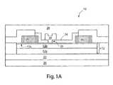
- FIG. 1Ais a cross-section of a gallium nitride material transistor building block structure that may be a portion of a gallium nitride material device according to one embodiment of the invention
- FIG. 1Bis a top view of a transistor building block structure
- FIG. 1Cis a plan view of a transistor unit cell
- FIG. 2Ais a top view of a unit cell configuration according to one embodiment of the present invention.
- FIG. 2Bis a schematic representation of a portion of the unit cell configuration of FIG. 2A ;
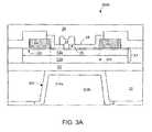
- FIG. 3Ais a cross-section of a gallium nitride material transistor building block including a via that surrounds an active region of the device according to an embodiment
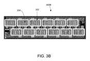
- FIG. 3Bshows a device including a plurality of vias that surround the source, gate and drain electrodes of each transistor in respective cells according to an embodiment
- FIG. 4is a schematic representation of a packaged device
- FIGS. 5 and 6are graphs illustrating performance characteristics of Devices A and B, as described in Example 1.
- the inventionprovides gallium nitride material devices and methods associated with the same.
- the devicesmay be designed to provide enhanced thermal conduction through and out of the device, while maintaining excellent electrical properties.
- the devicemay include a layout of transistors designed to increase removal of heat from the device.
- the layoutinvolves grouping the transistors into cells and spacing the cells an appropriate distance from each other.
- the layoutmay involve placing the cells in a staggered configuration.
- the heat flow through and out of gallium nitride devicesmay also be improved by using thermally conductive packaging arrangements and/or by removing selective portions (or all) of the substrate on which gallium nitride material regions are disposed.
- the increased thermal conduction through and out of the gallium nitride material devicesimproves performance by enabling devices to operate at high power densities, as well as increasing reliability and lifetime.
- FIGS. 1A and 1Brespectively illustrate a cross-section and top view of a transistor building block structure 10 that may be incorporated into a gallium nitride material device.
- Structure 10includes a gallium nitride material region 12 .
- the transistor structurealso includes a source electrode 14 , a drain electrode 16 and a gate electrode 18 formed on the gallium nitride material region.
- the gallium nitride material regionis formed on a substrate 20 and, as shown, a transition layer 22 may be formed between the substrate and the gallium nitride material region.
- the transistorincludes a passivating layer 24 that protects and passivates the surface of the gallium nitride material region.
- a via 26is formed within the passivating layer in which the gate electrode is in part formed.
- An encapsulation layer 28is formed over the gate electrode and passivation layer, amongst other features.
- the transistor structure shown in FIG. 1Ais illustrative, but should not be considered limiting. Other transistor structures, or other active or passive elements, may be used within the gallium nitride material devices according to aspects of the present invention.
- the term “device”may be an operable semiconductor device (e.g., a transistor) or a semiconductor device structure that needs additional processing to form an operable device.
- a structuree.g., layer, region
- itcan be directly on the structure, or an intervening structure (e.g., layer, region) also may be present.
- a structure that is “directly on” or “in contact with” another structuremeans that no intervening structure is present. It should also be understood that when a structure is referred to as being “on”, “over”, “overlying”, or “in contact with” another structure, it may cover the entire structure or a portion of the structure.
- a plurality of building block structures 10may be combined to construct a power transistor device. Suitable ways of combining the building block structures are known to those of skill in the art and have been described in commonly-owned U.S. Pat. No. 7,135,720 which is incorporated herein by reference and is based on U.S. patent application Ser. No. 10/913,297, filed Aug. 5, 2004.
- FIG. 1Cis a plan view of a transistor unit cell 30 .
- the transistor unit cellincludes ten transistor building block structures. As shown, the source electrodes in the unit cell are connected to a common source pad 32 ; the gate electrodes are connected to a common gate pad 34 ; and, the drain electrodes are connected to a common drain pad 36 . In the illustrative unit cell, ten gate electrodes are connected to the gate pad, six source electrodes are connected to source pad, and five drain electrodes are connected to the drain pad.
- the transistor unit cell 30is provided as an example, and other configurations of a unit cell are possible. For example, the transistor unit cell may include a different number of building block structures and/or have different types of electrode and pad connections.
- the gates of the transistor building block structuresare spaced by a gate pitch S.
- the gate pitchrepresents the distance from one gate to the gate of an adjacent transistor building block.
- the gate pitchmay be measured from the centerline of one gate to the centerline of the gate of an adjacent transistor building block structure.
- the gate pitch Sis uniform (i.e., the same) between the gates of adjacent transistor building blocks.
- the unit celldoes not need to have uniform gate spacing between the transistor building blocks, and may have different gate spacings in some embodiments.
- FIG. 2Ais a top view of a unit cell configuration of a gallium nitride material device 200 according to one embodiment of the present invention.
- the arrangement of the unit cellsreduces thermal resistance, thereby increasing thermal conduction, while also maintaining good RF parasitics.
- the gallium nitride material device 200comprises two rows, 202 A and 202 B, of unit cells. In the illustrated embodiment, each row comprises nine unit cells. However, the invention is not limited in the number of rows or the number of unit cells provided. For instance, the gallium nitride material device 200 may comprise between two and four rows, or any appropriate number of rows. In addition, each row may contain between two and ten unit cells, or any appropriate number of unit cells.
- row 202 Acomprises unit cells 204 A, 204 B, . . . , 204 I.
- Row 202 Bcomprises unit cells 204 J, 204 K, . . . , 204 R. In the illustrated embodiment, the unit cells 204 are identical. Furthermore, the unit cells 204 are identical to the unit cell 30 of FIG. 1C .
- FIG. 2Ais a schematic of a portion of the unit cell configuration illustrated in FIG. 2A .
- the inter-cell spacingmay be greater than the gate pitch S of the transistor building block structures within each unit cell.
- the inter-cell spacing Lmay be at least two times greater than gate pitch S. In some embodiments, the inter-cell spacing L may be at least three times the gate pitch S, or at least four times the gate pitch S.
- the inter-cell spacingmay be less than ten times, or less than eight times, the gate pitch S.
- Other spacingsmay also be appropriate and it should be recognized that the absolute values of the inter-cell spacing L and the gate pitch S may depend on the particular device. Suitable ranges for L include between 100 microns and 1000 microns (e.g., 300 microns), or between 50 and 300 microns. Suitable ranges for the gate pitch S include between 10 microns and 100 microns (e.g., 50 microns), or between 15 and 60 microns.
- the gate pitch S within each unit cellis not uniform. When the gate pitch S is not uniform, the inter-cell spacing L may be chosen so that L is greater than each gate pitch S within the unit cells; and, in some cases, at least two times, three times, or four times greater than the maximum gate pitch.
- FIGS. 2A and 2BAnother aspect of the layout of unit cells 204 illustrated in FIGS. 2A and 2B involves the relative placement of the rows 202 A and 202 B. As shown in FIGS. 2A and 2B , the rows 202 A and 202 B are staggered such that the units cells of row 202 A are not horizontally aligned with the unit cells in row 202 B.
- the “horizontal alignment” (or lack thereof) of a unit cell and another unit cellmay be assessed by comparing a relative position on one unit cell to the same relative position on the other unit.
- rows 202 A and 202 Bare not horizontally aligned since the uppermost gate (G 1 ) of one unit cell in row 202 A is not horizontally aligned with the uppermost gate (G 2 ) of a unit cell in row 202 B.
- the staggered layout of the unit cellsprovides additional pathways for heat flow that are not present when the unit cells are horizontally aligned with each other.
- the degree to which the rows 202 A and 202 B are staggeredcan be chosen to optimize thermal conduction while taking into account other design factors, such as the surface area required for the unit cell layout, electrical coupling, or other performance criteria.
- the rows 202 A and 202 Bmay be staggered such that the unit cells of row 202 A overlap the unit cells of row 202 B in the y-direction by an amount Y.
- the overlap Yis approximately equal to the gate pitch S of the transistor building block structures within the unit cells 204 .
- the overlap Ycan be chosen to be any appropriate distance and the invention is not limited in this respect.
- the gallium nitride material device 200may be configured to provide no overlap in the y-direction between the units cells of rows 202 A and 202 B.
- the overlap Yis between one and three times the gate pitch S. In some embodiments, the overlap Y is less than five times the gate pitch S. In absolute values, the overlap Y may be between 0 and 250 microns (e.g., 50 microns), or any appropriate value.
- inter-row spacing Xprovides for additional space between the unit cells 204 for thermal conduction.
- the inter-row spacingis approximately three to four times greater than the gate pitch S.
- the inter-row spacingis at least as great as the gate pitch S.
- the inter-row spacing Xis no greater than five times the gate pitch S.
- the inter-row spacingin some embodiments may be between 10 microns and 300 microns (e.g., 150 microns). However, any inter-row spacing may be chosen, and the invention is not limited in this respect.
- FIGS. 2A and 2Bare merely exemplary, and that the invention is not limited to those configurations.
- more than one row of unit cellsmay be used.
- a rowmay comprise any number of unit cells.
- the unit cellsneed not be arranged into rows.
- the various dimensions, such as the gate pitch, the inter-cell spacing, the inter-row spacing, and the overlapmay all be chosen to optimize thermal conduction through and out of the device, while taking into account other design criteria (e.g., electrical properties) for a given device application.
- portions, or all, of substrate 20may be removed to enhance thermal conduction. Portions of the substrate may be removed to form one or more vias proximate the active region(s) of the transistor(s).
- the term “active region”refers to a portion of the gallium nitride material region between the edge of the source electrode closest to the gate electrode and the edge of the drain electrode closest to the gate.
- the viamay define an area that surrounds the active regions of one, or more than one, of the transistors in a cell. It may be preferable for the via to surround the active region of each transistor in the cell. Such a via may be associated with each unit cell of the device.
- the term “surround” in this contextrefers to vias that encompass the active region within the footprint defined by the via. It should be understood that the via may be formed entirely in regions below the active region including regions below the gallium nitride material region such as in the substrate.
- the viacan surround a larger region than the active region.
- the viamay surround the source electrode, drain electrode and gate electrode of one, or more than one, of the transistors in a cell.
- Such a viamay be associated with each unit cell of the device.
- FIGS. 3A and 3Bshow respective devices 300 A and 300 B including a plurality of vias 302 that surround active regions 303 of each transistor in respective cells 204 .
- the viasalso surround the source electrode, drain electrode and gate electrode of each transistor in respective cells 204 .
- devices of the inventionmay also include other vias that extend from a substrate surface that do not surround active regions. These vias may be present along with vias that do surround active regions but the primary purpose of such vias may be to provide an electrical conductive pathway, rather than to provide a thermal pathway. Such vias may extend all the way through the device, for example, from a source electrode to a backside of the device as described in commonly-owned U.S. patent application Ser. No. 11/634,332, filed Dec. 4, 2006, which is incorporated herein by reference. In some embodiments, the devices may be free of vias.
- via 302extends from a back surface 312 of substrate 20 .
- the viamay extend through the entire thickness of the substrate (as shown), or only a portion of the thickness. It is also possible for the via to extend into the overlying epitaxial layers including transition layer 22 and/or gallium nitride material region 12 .
- the substratemay be an SOI (silicon on insulator) substrate which includes a lower silicon portion, an insulator portion (e.g., silicon oxide) layer formed on the lower silicon portion and an upper portion.
- the viamay extend through the lower silicon portion ending at the insulating portion which can function as an etch stop during processing.
- the via(s)may define an area that surrounds the active region in the overlying gallium nitride material region. Such a structure can be a particularly well-suited for heat removal as described further below. In other embodiments, the via may not surround the active region, but may only surround a portion of the active region.
- the viasmay be formed using any suitable technique such as etching.
- localized viasmay not be formed and the substrate, for example, may be thinned across its entire area. It may be advantageous to thin the substrate when the substrate comprises silicon in order to limit the effects of the relatively poor thermal conductivity properties of silicon on the overall thermal conduction from the device.
- the substratemay be thinned to a thickness of less than 120 micron, or less than 75 microns (e.g., 50 microns). In some cases, it may be preferable that the substrate is at least 10 microns thick to provide mechanical stability to the structure. However, in some embodiments, the entire substrate may be removed across the entire device, as described further below.
- the devicesare free of a substrate on which the gallium nitride material region is formed.
- Substrate thinning and/or removalmay be done using any suitable technique such as etching or grinding/polishing.
- a thermally conductive material region 314may be formed, at least in part, in the via.
- the thermally conductive material regioncan lead to greater heat flow by providing a more highly conductive thermal pathway from the active region to ambient (e.g., in some cases, through a package which may also be thermally conductive as described further below).
- the viamay be entirely filled with thermally conductive material, though, in others only a portion of the via is filled.
- the thermally conductive material regionmay comprise a single thermally conductive material or a combination of more than one thermally conductive material (e.g., 314 a , 314 b as shown).
- the thermally conductive material(s)generally have a thermal conductivity (e.g., at room temperature) greater than that of the substrate, particularly if the substrate is silicon.
- Suitable materialsinclude metals (e.g., copper, gold, silver) and dielectric materials (e.g., diamond, carbon-based materials including carbon nanotubes, aluminum nitride, and silicon carbide).
- the thermally conductive material region in the viaincludes a dielectric material portion 314 a and a metal portion 314 b .
- the thermally conductive material regionincludes only a dielectric material portion, or only a metal portion.
- metal portion 314 bmay be grounded.
- the dielectric material portionseparates the metal region from the epitaxial layers (e.g., transition layer 22 , gallium nitride material region 12 ) above.
- the separation distance between the metal portion and the gate electrode and/or the dielectric properties of the material(s)can be important to the resulting electrical properties of the device. For example, proper selection of the separation distance and the dielectric constant can minimize (or reduce) power loss through capacitance effects that could arise as a result of the metal portion and the gate electrode.
- the dielectric constantmay be 15 or less; in some cases, 10 or less (e.g., 8-9).
- the vertical separation distance between the metal portion and the gate electrodeis between 0.5 microns and 50 microns; and, in some cases, between 5 microns and 50 microns.
- the vertical separation distancemay be between 0.5 microns and 2.5 microns, or 0.5 microns and 5.0 microns. Other ranges may also be suitable and, for example, may depend on the dielectric constant of the material separating the metal portion and the gate electrode.
- it may be preferable for the vertical separation distance between the metal portion and the gate electrodeto be greater than the lateral separation distance between the gate electrode and the drain electrode.
- thermally conductive regions being formed in via(s)also generally pertains to embodiments in which the substrate is thinned and/or removed. That is, the above-noted thermally conductive material regions (including material regions having a dielectric material portion and a metal portion) may be formed on the backside of a thinned substrate, or the backside of the epitaxial layer stack (e.g., transition layer 22 , gallium nitride material region 12 ) when the substrate is removed.
- the thermally conductive material regionmay be formed using conventional deposition or bonding techniques depending on the material type and layer configuration. For example, when the thermally conductive material region is formed in a via, the region may be deposited/patterned using suitable conventional techniques; and, when the thermally conductive material region is formed on the backside of a thinned substrate or backside of the epitaxial layer stack, the thermally conductive material region may be deposited or may be bonded to the appropriate backside using conventional techniques.
- Packaged device 400includes device 402 mounted on a supporting portion 403 of a package 404 .
- the packagemay also include an upper portion (not shown) which surrounds or encapsulates the top of the device.
- the upper portionif present, may be formed of a ceramic or polymeric material, for example.
- the package, and in particular the supporting portion, 404may also be configured to enable efficient thermal conduction.
- the packagemay comprise a suitable thermally conductive material, such as a metal or dielectric material.
- the supporting portionmay consist essentially of copper (i.e., non-alloyed copper).
- heat generated by the devicescan be dissipated through the package to the ambient environment.
- the thermally conductive material region 314may be in thermal (e.g., direct) contact with the supporting portion of the package.
- the thermally conductive material regionmay be copper and may be in thermal contact with the copper supporting portion.
- a pre-bowed packagemay be used, particularly when the package is a copper material.
- the extent of pre-bowingis selected so that the resulting interface 406 between the device and the package is substantially flat after processing.
- the packagemay have a convex shape and may include a bow (i.e., maximum distance that a portion deviates from the original plane) of between 25 micron and 125 micron. The selection is based on an understanding of the different rates of expansion experienced by the package material and the device during attachment.
- a pre-bowed copper packagemay be stressed using conventional techniques prior to attachment to the device which leads to its bowing.
- the process of attaching the device to the packagecan be accomplished by a eutectic attach process.
- the deviceis attached to the package 304 using a gold-tin eutectic attach process.
- the attaching materialmay be formed of a thermally and electrically conducting material (e.g., metal, certain epoxies) so that a thermally and electrically conducting pathway (e.g., formed entirely of metal) extends from the thermally conductive material in the device through the package.
- a thermally and electrically conducting materiale.g., metal, certain epoxies
- a thermally and electrically conducting pathwaye.g., formed entirely of metal
- the combination of the above-described via/thermally conductive material region formation and packaging techniquesmay provide particularly good thermal conduction.
- Gallium nitride material devices of the inventioncan have lower total thermal resistances than certain conventional devices by employing one or more of the above-described techniques for increasing thermal conduction.
- Thermal resistanceis a measure of transmit heat from the device, and may be determined by the temperature rise divided by the power dissipated by the device (expressed in units of ° C./W dissipated power ). The thermal resistance may be measured using known techniques such as IR imaging.
- a gallium nitride material device(based on transistors) having a total gate width of 36 mm (i.e., a 36 mm device) or larger can have a total thermal resistance, R jc of less than 1.5° C./W.
- the total thermal resistance of a 36 mm (or larger) gallium nitride material deviceis less than 1.0° C./W.
- the total thermal resistance of a 36 mm (or larger) gallium nitride material deviceis less than 0.85° C./W, or even less than 0.6° C./W.
- a 10 mm or larger gallium nitride material devicehas a total thermal resistance less than approximately 4° C./W; or less than 2° C./W. It should be understood that the “total gate width” refers to the sum of the width of each gate electrode in the device.
- the above-noted thermal propertiesmay be achieved while maintaining excellent electrical properties, particularly for RF applications, including high drain efficiency, output power, and gain amongst other properties.
- the gallium nitride material devices(including the devices having the thermal properties noted above) described herein may achieve the electrical properties of devices described in commonly-owned U.S. Pat. No. 7,135,720 which is incorporated herein by reference and commonly-owned U.S. patent application Ser. No. 11/543,010 which is also incorporated herein by reference.
- the devicescan achieve the following properties.
- Devices of the inventionmay operate at efficiencies of greater than or equal to 20% (e.g., between 22% and 30%).
- Efficiencyi.e., drain efficiency
- the devicesoperate at efficiencies of greater than or equal to 30%; and, in some embodiments, the devices operate at efficiencies of greater than or equal to 40%.
- efficiencies of less than or equal to 50%may be desired to limit sacrifices to other properties.
- the efficiencymay be controlled, in part, by the matching network, operating conditions and other design features (e.g., layer composition, gate length, gate pitch, amongst others).
- Output powermay be measured using standard techniques. It may be useful to express output power in terms of power density which is the output power divided by the gate periphery (W/mm). The output power depends largely on the size of the device. In some cases, the average output power is between about 0.5 W and about 40 W under OFDM modulation. Devices of the invention may have power densities of greater than or equal to 0.1 W/mm. In some embodiments, the power density may be greater than or equal to 0.5 W/mm; and, in some embodiments, the power density may be greater than or equal to 1.0 W/mm. In some cases, power densities of less than or equal to 10 W/mm may be desired to limit sacrifices to other properties. The power density may be controlled, in part, by the matching network, operating conditions and other design features (e.g., layer composition, gate length, gate pitch, amongst others).
- the devicesmay also operate at sufficient gains for RF power transistors markets (including wideband applications).
- Gainis defined as the output power divided by the input power and may be expressed in units of dB.
- the devicesmay have a gain of greater than or equal to 5 dB. In some embodiments, the gain may be greater than or equal to 12 dB (e.g., between 12 and 15). In some cases, a gain of less than or equal to 18 dB may be desired to limit sacrifices to other properties.
- the devicesare operated at drain voltages of up to 300 Volts.
- the drain voltagemay be up to 100 Volts or up to 50 Volts (e.g., 12 Volts, 28 Volts or 48 Volts).
- Suitable gate voltagesmay be between 0 Volts and ⁇ 10 Volts.
- the devices of the inventionmay be operated in frequency ranges between about 100 MHz and about 10 GHz; and, in some cases, within a frequency range of between about 1.8 and about 6 GHz (e.g., 3.3-3.8 GHz; or 2.3-2.7 GHz; or about 5.8 GHz). It should be understood that, in these embodiments, the input and/or output signal of the devices may be within these frequency ranges.
- devices of the inventionmay advantageously exhibit the above-noted property values (i.e., efficiency, output power, power density, gain) over a fairly wide frequency range.
- the above-noted property valuesmay be exhibited over a bandwidth of at least 100 MHz in some embodiments; or, in other embodiments, at least 200 MHz.
- gallium nitride material region 12 of the transistor structurefunctions as the active region. That is, the conductive channel extending from the source electrode to the drain electrode is formed in the gallium nitride material region.
- the gallium nitride material regioncomprises at least one gallium nitride material layer.
- gallium nitride materialrefers to gallium nitride (GaN) and any of its alloys, such as aluminum gallium nitride (Al x Ga (1-x) N), indium gallium nitride (In y Ga (1-y) N), aluminum indium gallium nitride (Al x In y Ga (1-X-y) N), gallium arsenide phosphoride nitride (GaAs a P b N (1-a-b) ), aluminum indium gallium arsenide phosphoride nitride (Al x In y Ga (1-x-y) As a P b N (1-a-b) ), amongst others.
- Gallium nitride materialsmay be doped n-type or p-type, or may be intrinsic. Suitable gallium nitride materials have been described in commonly-owned U.S. Pat. No. 6,649,287 incorporated herein by reference.
- the gallium nitride material regionincludes only one gallium nitride material layer. In other cases, the gallium nitride material region includes more than one gallium nitride material layer.
- the gallium nitride material regionmay include multiple layers ( 12 a , 12 b , 12 c ), as shown. In certain embodiments, it may be preferable for the gallium nitride material of layer 12 b to have an aluminum concentration that is greater than the aluminum concentration of the gallium nitride material of layer 12 a .
- the value of x in the gallium nitride material of layer 12 bmay have a value that is between 0.05 and 1.0 greater than the value of x in the gallium nitride material of layer 12 a , or between 0.05 and 0.5 greater than the value of x in the gallium nitride material of layer 12 a .
- layer 12 bmay be formed of Al 0.26 Ga 0.74 N, while layer 12 a is formed of GaN. This difference in aluminum concentration may lead to formation of a highly conductive region at the interface of the layers 12 a , 12 b (i.e., a 2-D electron gas region).
- layer 12 cmay be formed of GaN.
- Gallium nitride material region 12also may include one or more layers that do not have a gallium nitride material composition such as other III-V compounds or alloys, oxide layers, and metallic layers.
- the gallium nitride material regionis of high enough quality so as to permit the formation of devices therein.
- the gallium nitride material regionhas a low crack level and a low defect level.
- transition layer 22(particularly when compositionally-graded) may reduce crack and/or defect formation.
- Gallium nitride materials having low crack levelshave been described in U.S. Pat. No. 6,649,287 incorporated by reference above.
- the gallium nitride material regiona crack level of less than 0.005 m/m 2 .
- the gallium nitride material regionhas a very low crack level of less than 0.001 m/m 2 .
- gallium nitride materials having low dislocation densitiesmay be preferred. Suitable gallium nitride materials and processes for forming the same are described in commonly-owned, co-pending U.S. patent application Ser. No. 10/886,506, filed Jul. 7, 2004, entitled “III-Nitride Materials Including Low Dislocation Densities and Methods Associated With the Same”.
- the gallium nitride material regionincludes a layer or layers which have a monocrystalline structure. In some cases, the gallium nitride material region includes one or more layers having a Wurtzite (hexagonal) structure.
- the thickness of the gallium nitride material region and the number of different layersare dictated, at least in part, by the requirements of the specific device. At a minimum, the thickness of the gallium nitride material region is sufficient to permit formation of the desired structure or device.
- the gallium nitride material regiongenerally has a thickness of greater than 0.1 micron, though not always. In other cases, gallium nitride material region 12 has a thickness of greater than 0.5 micron, greater than 0.75 micron, greater than 1.0 microns, greater than 2.0 microns, or even greater than 5.0 microns.
- the deviceincludes passivating layer 24 formed on the surface of gallium nitride material region 12 .
- Suitable passivating layers(some of which also function as electrode-defining layers) have been described in commonly-owned, co-pending U.S. Pat. No. 7,071,498, filed Dec. 17, 2003, entitled “Gallium Nitride Material Devices Including an Electrode-Defining Layer and Methods of Forming The Same”, which is incorporated herein by reference.
- Suitable compositions for passivating layer 24include, but are not limited to, nitride-based compounds (e.g., silicon nitride compounds), oxide-based compounds (e.g., silicon oxide compounds), polyimides, other dielectric materials, or combinations of these compositions (e.g., silicon oxide and silicon nitride).
- nitride-based compoundse.g., silicon nitride compounds
- oxide-based compoundse.g., silicon oxide compounds
- polyimidese.g., other dielectric materials
- other dielectric materialse.g., silicon oxide and silicon nitride
- the passivating layerit may be preferable for the passivating layer to be a silicon nitride compound (e.g., Si 3 N 4 ) or non-stoichiometric silicon nitride compounds.
- substrate 20is a silicon substrate. Silicon substrates may be preferred because they are readily available, relatively inexpensive and are of high crystalline quality.
- a silicon substraterefers to any substrate that includes a silicon surface.
- suitable silicon substratesinclude substrates that are composed entirely of silicon (e.g., bulk silicon wafers), silicon-on-insulator (SOI) substrates, silicon-on-sapphire substrate (SOS), and SIMOX substrates, amongst others.
- Suitable silicon substratesalso include substrates that have a silicon wafer bonded to another material such as diamond, AlN, or other polycrystalline materials. Silicon substrates having different crystallographic orientations may be used. In some cases, silicon (111) substrates are preferred. In other cases, silicon (100) substrates are preferred.
- the silicon substrate(or at least the silicon portion of the substrate for substrates that include a silicon portion formed on another material) is highly resistive.
- the resistivity of the silicon substratemay be greater than or equal to about 10 2 Ohms-cm.
- the resistivity of the substratemay be greater than or equal to about 10 4 Ohms-cm; or even, greater than or equal to about 10 5 Ohms-cm.
- Highly resistive silicon substratesmay be particularly preferred in structures that are used to form devices that operate at high frequencies (e.g., RF devices).
- the high resistivitycan reduce so-called substrate losses which otherwise may arise and sacrifice performance. These substrate losses may render silicon substrates with lower resistivities unsuitable in high frequency devices.
- Suitable highly resistive silicon substratehave been described in commonly-owned U.S. Patent Publication No. 2006-0118819 which is based on U.S. patent application Ser. No. 11/004,628 filed Dec. 3, 2004.
- substratesmay also be used including sapphire, silicon carbide, indium phosphide, silicon germanium, gallium arsenide, gallium nitride material, aluminum nitride, or other III-V compound substrates.
- silicon substratesmay also be used including sapphire, silicon carbide, indium phosphide, silicon germanium, gallium arsenide, gallium nitride material, aluminum nitride, or other III-V compound substrates.
- silicon substratesin embodiments that do not use silicon substrates, all of the advantages associated with silicon substrates may not be achieved.
- Substrate 20may have any suitable dimensions and its particular dimensions are dictated, in part, by the application and the substrate type. Suitable diameters may include, but are not limited to, 2 inches (50 mm), 4 inches (100 mm), 6 inches (150 mm), and 8 inches (200 mm).
- the substratemay be relatively thick, such as greater than about 125 micron (e.g., between about 125 micron and about 800 micron, or between about 400 micron and 800 micron). Relatively thick substrates may be easy to obtain, process, and can resist bending which can occur, in some cases, when using thinner substrates. In other embodiments, thinner substrates (e.g., less than 125 microns) are used. Though thinner substrates may not have the advantages associated with thicker substrates, thinner substrates can have other advantages including facilitating processing and/or reducing the number of processing steps. In some processes, the substrate initially is relatively thick (e.g., between about 200 microns and 800 microns) and then is thinned during a later processing step (e.g., to less than 150 microns).
- a later processing stepe.g., to less than 150 microns.
- the substrateis substantially planar in the final device or structure.
- Substantially planar substratesmay be distinguished from substrates that are textured and/or have trenches formed therein (e.g., as in U.S. Pat. No. 6,265,289).
- the regions/layers formed on the substratee.g., transition layer, gallium nitride material region, and the like
- such regions/layersmay be grown in vertical (e.g., non-lateral) growth processes.
- Planar substrates and regions/layerscan be advantageous in some embodiments, for example, to simplify processing. Though it should be understood that, in some embodiments of the invention, lateral growth processes may be used as described further below.
- Transition layer 22may be formed on substrate 20 prior to the deposition of gallium nitride material region 12 .
- the transition layermay accomplish one or more of the following: reducing crack formation in the gallium nitride material region 12 by lowering thermal stresses arising from differences between the thermal expansion rates of gallium nitride materials and the substrate; reducing defect formation in gallium nitride material region by lowering lattice stresses arising from differences between the lattice constants of gallium nitride materials and the substrate; and, increasing conduction between the substrate and gallium nitride material region by reducing differences between the band gaps of substrate and gallium nitride materials.
- the presence of the transition layermay be particularly preferred when utilizing silicon substrates because of the large differences in thermal expansion rates and lattice constant between gallium nitride materials and silicon. It should be understood that the transition layer also may be formed between the substrate and gallium nitride material region for a variety of other reasons. In some cases, for example when a silicon substrate is not used, the device may not include a transition layer.
- the composition of transition layer 22depends, at least in part, on the type of substrate and the composition of gallium nitride material region 12 .
- the transition layermay comprise a III-nitride material (i.e., gallium nitride (GaN), aluminum nitride (AlN), indium nitride (InN) and their respective alloys (e.g., AlGaN, InGaN, AlInGaN and AlInN)).
- the transition layermay preferably comprise a compositionally-graded transition layer having a composition that is varied across at least a portion of the layer. Suitable compositionally-graded transition layers, for example, have been described in commonly-owned U.S. Pat. No.
- compositionally-graded transition layersare particularly effective in reducing crack formation in the gallium nitride material region by lowering thermal stresses that result from differences in thermal expansion rates between the gallium nitride material and the substrate (e.g., silicon).
- the compositionally-graded, transition layeris formed of an alloy of gallium nitride such as Al x In y Ga (1-x-y) N, Al x Ga (1-x) N, or In y Ga (1-y) N, wherein 0 ⁇ x ⁇ 1, 0 ⁇ y ⁇ 1.
- the concentration of at least one of the elements (e.g., Ga, Al, In) of the alloyis typically varied across at least a portion of the cross-sectional thickness of the layer.
- the transition layerhas an Al x In y Ga (1-x-y) N composition
- x and/or ymay be varied
- the transition layerhas a Al x Ga (1-x) N composition
- xmay be varied
- ymay be varied.
- the transition layermay have a low gallium concentration at a back surface which is graded to a high gallium concentration at a front surface. It has been found that such transition layers are particularly effective in relieving internal stresses within the gallium nitride material region.
- the transition layermay have a composition of Al x Ga (1-x) N, where x is decreased from the back surface to the front surface of the transition layer (e.g., x is decreased from a value of 1 at the back surface of the transition layer to a value of 0 at the front surface of the transition layer).
- the composition of the transition layerfor example, may be graded discontinuously (e.g., step-wise) or continuously.
- One discontinuous grademay include steps of AlN, Al 0.6 Ga 0.4 N and Al 0.3 Ga 0.7 N proceeding in a direction toward the gallium nitride material region.
- the transition layerhas a monocrystalline structure.
- transition layer 22has a constant (i.e., non-varying) composition across its thickness.
- the source, drain and gate electrodesmay be formed of any suitable conductive material such as metals (e.g., Au, Ni, Pt, Ti, Al, Ta, W), metal compounds (e.g., WSi, WSiN), alloys, semiconductors, polysilicon, nitrides, or combinations of these materials.
- the dimensions of the gate electrodecan be important to device performance.
- via 26 formed in the passivating layerdefines (at least in part) the gate electrode dimensions. Thus, by controlling the shape of the via, it is possible to define desired gate dimensions. Suitable via and gate dimensions have been described in U.S.
- electrodesmay extend into the gallium nitride material region.
- electrode materiale.g., metal
- deposited on the surface of the gallium nitride material regionmay diffuse into the gallium nitride material region during a subsequent annealing step (e.g., RTA) when forming the electrode.
- the source and drain electrodesmay include such a portion diffused into the gallium nitride material region. As used herein, such electrodes are still considered to be formed on the gallium nitride material region.
- Source, gate and drain padsmay be formed of any suitable conductive material such as metals (e.g., Au, Ni, Pt, Ti, Al, Ta, W), metal compounds (e.g., WSi, WSiN), alloys, semiconductors, polysilicon, nitrides, or combinations of these materials.
- the padsare formed of the same material as the corresponding electrodes.
- the device shown in FIGS. 1A and 1Balso includes an encapsulation layer 28 which, as known to those of skill in the art, encapsulates underlying layers of the structure to provide chemical and/or electrical protection.
- the encapsulation layermay be formed of any suitable material including oxides or nitrides.
- the transistor structuremay include other layers.
- the transistor structuremay include additional features not shown in FIGS. 1A and 1B .
- the transistor structuremay include a strain-absorbing layer formed directly on the surface of substrate 20 . Suitable strain-absorbing layers have been described in commonly-owned, co-pending U.S. Patent Application Publication No. 20050285141, which is incorporated herein by reference and is based on U.S. patent application Ser. No. 10/879,703, entitled “Gallium Nitride Materials and Methods Associated With the Same”, filed Jun. 28, 2004.
- intermediate layersmay be present. Suitable intermediate layers, for example, have been described and illustrated in U.S. Pat. No. 6,649,287, which was incorporated by reference above. In other embodiments of the invention, layer(s) shown herein may not be present. Other variations to the structures and devices shown herein would be known to those of skill in the art and are encompassed by the present invention.
- Structures and devices of the present inventionmay be formed using methods that employ conventional processing techniques.
- the stack of material layersis formed on a substrate which is later processed (e.g., diced) to form the desired final structure (e.g., transistor).
- the layers and regions of the transistor structure of FIGS. 1A and 1Bmay be formed, patterned, etched and implanted using conventional techniques.
- Transition layer 22 and gallium nitride material region 12may be deposited, for example, using metal organic chemical vapor deposition (MOCVD), molecular beam epitaxy (MBE), and hydride vapor phase epitaxy (HVPE), amongst other techniques.
- MOCVDmetal organic chemical vapor deposition
- MBEmolecular beam epitaxy
- HVPEhydride vapor phase epitaxy
- the preferred techniquemay depend, in part, on the composition of the layers.
- An MOCVD processmay be preferred.
- a suitable MOCVD process to form a transition layer (e.g., a compositionally-graded transition layer) and gallium nitride material region over a silicon substratehas been described in U.S. Pat. No. 6,649,287 incorporated by reference above.
- a single deposition stepe.g., an MOCVD step
- the processing parametersare suitably changed at the appropriate time to form the different layers.
- a single growth stepmay be used to form the transition layer and the gallium nitride material region.
- the stress-absorbing layermay be formed using techniques described in U.S. patent application Ser. No. 10/879,703 which is incorporated by reference above.
- Passivating layer 24may be deposited using any suitable technique.
- CVDchemical vapor deposition
- PECVDplasma vapor deposition
- LP-CVDLP-CVD
- ECR-CVDLP-CVD
- ICP-CVDICP-CVD
- evaporation and sputteringevaporation and sputtering.
- via 26may be formed within the passivating layer using an etching technique.
- a plasma etching techniqueis preferably used to form the via with controlled dimensions
- Source, drain and gate electrodesmay be deposited on the gallium nitride material region using known techniques such as an evaporation technique. In cases when the electrodes include two metals, then the metals are typically deposited in successive steps. The deposited metal layer may be patterned using conventional methods to form the electrodes. In some embodiments, an annealing step (e.g., RTA) may also be used in which the deposited electrode material diffuses into the gallium nitride material region, particularly when forming source and drain electrodes.
- RTAannealing step
- Source, drain and gate electrode padsmay also be deposited and patterned using known techniques.
- an isolation regionmay be formed which electrical isolates the active region. Suitable processes for forming isolation region have been described in commonly owned U.S. Patent Application Publication No. 2005/0145851, which is based on U.S. patent application Ser. No. 10/879,795, filed Jun. 28, 2004, entitled “Gallium Nitride Material Structures Including Isolation Regions and Methods”, which is incorporated herein by reference above.
- the above-described processesare used to form a semiconductor wafer including the desired material layers and features.
- the wafermay be further processed using conventional techniques to produced desired device structures.
- the wafermay be thinned from its backside.
- a metallic layere.g., Au, Ti, Sn
- the wafermay be diced to form devices structure (e.g., die) which can be further processed.
- the device structuresWhen mounting on a package, the device structures may be placed in the package and subjected to a heating step sufficient to weld the device structure to the packaging material.
- the transistorsare mounted to other entities (e.g., a heat sink) using known techniques.
- This exampledescribes production and characterization of gallium nitride material devices implementing some of the aspects of the present invention, as well as a comparison to conventional gallium nitride material devices.
- Device A and Device Bcomprised a gallium nitride material region of undoped III-N heterostructures grown on high resistivity Si (111) substrates by metal organic chemical vapor deposition.
- the deviceswere formed of transistor unit cells similar to those shown in cross-section in FIG. 1 , though the unit cell layout in Devices A and B were different.
- Device Aemployed a standard transistor layout
- Device Bemployed a staggered transistor layout similar to that shown in FIG. 2A
- Device Aincluded a single row of transistor cells with each transistor having a gate pitch of 30 micron.
- Device Bthe cells were arranged in two rows, providing room for a gate pitch of 50 ⁇ m.
- the increased gate pitchreduced thermal coupling, or interaction between adjacent heat sources (the active regions within the unit cells).
- Device A and Device Bhad the same total gate width.
- Device A and Device Bwere both packaged.
- Device Awas attached to a high thermal conductivity Cu—Mo laminate (CPC) single-ended ceramic package using a AuSi eutectic die attach process.
- Device Bwas attached to a high thermal conductivity pure copper (Cu) single-ended, ceramic package, using a AuSn eutectic die attach process.
- the sourceswere grounded to the package base through backside vias in the silicon die.
- Device Binclude a silicon substrate thinned to about 100 micron, while Device A had a 150 micron thick silicon substrate.
- a 2-stage internal matching networkwas used to transform the input impedance, while no intentional internal matching existed on the output.
- the packaged deviceswere mounted to an aluminum-based fixture which functioned, in part, as a heat sink and infrared (IR) measurements were made using a Quantum Focus Instruments (QFI) InfraScope II thermal imaging system, available from Quantum Focus Instruments Corporation (Vista, Calif.).
- QFIQuantum Focus Instruments
- the dissipated power of the deviceswas produced by direct current (DC) for convenience.
- the drain voltagewas held at 28 V and the gate voltage was varied to achieve different drain current levels and hence different power dissipations.
- the heat sink temperaturewas maintained at 80° C. to reduce background radiant energy.
- an image using the 1 ⁇ lenswas taken to determine the location of peak channel temperature and to check the thermal distribution across the entire device.
- a 15 ⁇ lens with ⁇ 2.5 ⁇ m spatial resolutionwas then used to obtain the peak channel temperature.
- the temperature at the back of the packagewas measured using a thermocouple passing through an aperture in the heat sink and contacting the bottom of the package.
- the thermal resistancewas calculated from the channel to the back of the package/case (R JC ).
- Device Ahad a thermal resistance of 1.95° C./W and Device B had a significantly lower thermal resistance of 0.85° C./W.
- RF measurementswere made with a standard load pull system using Focus Microwaves, Inc. tuners. RF characteristics were taken at a drain voltage of 40V. The devices were biased in class AB with approximately 55 mA quiescent drain current and the impedances were optimized to obtain maximum RF output power.
- MTTFmean time to failure
- FIG. 5illustrates RF performance of Device A (closed circles) and Device B (open triangles). Collapse of the efficiency and gain for Device A was seen at an output power of about 46 dBm (about 40 W). Device B achieved about 51 dBm (about 126 W) with 56% efficiency without collapse, demonstrating the benefits of the thermal design of Device B.
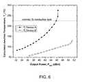
- FIG. 6shows the corresponding calculated channel temperature for Devices A and B.
- the closed circlescorrespond to Device A and the open triangles correspond to Device B.
- the temperature of the points shown in the graphis calculated using the measured output power, gain, efficiency, and the thermal resistance obtained from IR measurement and simulation.
- CWcontinuous waveform
- P D86.7 W
- ⁇ T JC169° C.
- Device Bwould only have a junction temperature of ⁇ 165° C. when operated under CW conditions and with 90° C. case temperature.
- the improved thermal performance of Device Ballows it to operate with good RF performance and with an acceptable MTTF even under the most stringent conditions of CW operation and elevated case temperature.
- this exampledemonstrates the benefits obtained in terms of thermal conduction through and out of the device and electrical performance by utilizing aspects of the present invention in a gallium nitride material device.
Landscapes
- Engineering & Computer Science (AREA)
- Chemical & Material Sciences (AREA)
- Materials Engineering (AREA)
- Physics & Mathematics (AREA)
- Condensed Matter Physics & Semiconductors (AREA)
- General Physics & Mathematics (AREA)
- Computer Hardware Design (AREA)
- Microelectronics & Electronic Packaging (AREA)
- Power Engineering (AREA)
- Ceramic Engineering (AREA)
- Junction Field-Effect Transistors (AREA)
Abstract
Description
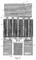
| TABLE I |
| Device Comparison |
| Quantity | Device A | Device B | ||
| Layout | Standard | Staggered Unit Cells | ||
| 36 | 36 mm | |||
| 200 | 200 | |||
| Gate Pitch | ||||
| 30 | 50 μm | |||
| Package Thermal | 240 W/m-K | 400 W/m-K | ||
| Conductivity | (CPC) | (Cu) | ||
| Package Thickness | 1000 micron | 1000 | ||
| Si Thickness | ||||
| 150 | 100 micron | |||
| Attach Material | AuSi | AuSn | ||
| Die Size | 1 × 6 mm | 1.2 × 6 mm | ||
| RJC | 1.95° C./W | 0.85° C./W | ||
Claims (16)
Priority Applications (1)
| Application Number | Priority Date | Filing Date | Title |
|---|---|---|---|
| US11/839,040US7745848B1 (en) | 2007-08-15 | 2007-08-15 | Gallium nitride material devices and thermal designs thereof |
Applications Claiming Priority (1)
| Application Number | Priority Date | Filing Date | Title |
|---|---|---|---|
| US11/839,040US7745848B1 (en) | 2007-08-15 | 2007-08-15 | Gallium nitride material devices and thermal designs thereof |
Publications (1)
| Publication Number | Publication Date |
|---|---|
| US7745848B1true US7745848B1 (en) | 2010-06-29 |
Family
ID=42271175
Family Applications (1)
| Application Number | Title | Priority Date | Filing Date |
|---|---|---|---|
| US11/839,040ActiveUS7745848B1 (en) | 2007-08-15 | 2007-08-15 | Gallium nitride material devices and thermal designs thereof |
Country Status (1)
| Country | Link |
|---|---|
| US (1) | US7745848B1 (en) |
Cited By (27)
| Publication number | Priority date | Publication date | Assignee | Title |
|---|---|---|---|---|
| US20100258844A1 (en)* | 2009-04-08 | 2010-10-14 | Alexander Lidow | BUMPED, SELF-ISOLATED GaN TRANSISTOR CHIP WITH ELECTRICALLY ISOLATED BACK SURFACE |
| US20110169014A1 (en)* | 2010-01-12 | 2011-07-14 | Sumitomo Electric Industries, Ltd. | Compound semiconductor device |
| WO2012158464A3 (en)* | 2011-05-17 | 2013-01-24 | Hrl Laboratories, Llc | Gan hemts with a back gate connected to the source |
| US8384130B2 (en)* | 2011-04-25 | 2013-02-26 | Samsung Electro-Mechanics Co., Ltd. | Nitride semiconductor device having a two-dimensional electron gas (2DEG) channel |
| WO2013142156A1 (en)* | 2012-03-20 | 2013-09-26 | Northrop Grumman Systems Corporation | Direct growth of diamond in backside vias for gan hemt devices |
| US20140264361A1 (en)* | 2013-03-15 | 2014-09-18 | Hrl Laboratories, Llc | Iii-nitride transistor with engineered substrate |
| WO2014152598A1 (en)* | 2013-03-15 | 2014-09-25 | The Government Of The United States Of America, As Represented By The Secretary Of The Navy | Nanocrystalline diamond three-dimensional films in patterned semiconductor substrates |
| WO2014202409A1 (en)* | 2013-06-18 | 2014-12-24 | Robert Bosch Gmbh | Transistor and method for producing a transistor |
| WO2015027080A3 (en)* | 2013-08-22 | 2015-04-16 | Northrop Grumman Systems Corporation | Selective deposition of diamond in thermal vias |
| US20150243848A1 (en)* | 2010-02-12 | 2015-08-27 | Tsmc Solid State Lighting Ltd. | Light-emitting devices with through-substrate via connections |
| CN105140281A (en)* | 2015-05-27 | 2015-12-09 | 苏州能讯高能半导体有限公司 | Semiconductor device and manufacturing method thereof |
| US9559056B2 (en) | 2014-09-18 | 2017-01-31 | Infineon Technologies Austria Ag | Electronic component |
| US9954529B2 (en)* | 2016-02-18 | 2018-04-24 | International Business Machines Corporation | Ultra dense vertical transport FET circuits |
| US9991776B2 (en) | 2015-12-16 | 2018-06-05 | Semiconductor Components Industries, Llc | Switched mode power supply converter |
| US10541323B2 (en) | 2016-04-15 | 2020-01-21 | Macom Technology Solutions Holdings, Inc. | High-voltage GaN high electron mobility transistors |
| US10651317B2 (en) | 2016-04-15 | 2020-05-12 | Macom Technology Solutions Holdings, Inc. | High-voltage lateral GaN-on-silicon Schottky diode |
| US10950598B2 (en) | 2018-01-19 | 2021-03-16 | Macom Technology Solutions Holdings, Inc. | Heterolithic microwave integrated circuits including gallium-nitride devices formed on highly doped semiconductor |
| CN112786449A (en)* | 2019-11-07 | 2021-05-11 | 上海华为技术有限公司 | HEMT device manufacturing method, HEMT device and radio frequency power amplifier |
| US11056483B2 (en) | 2018-01-19 | 2021-07-06 | Macom Technology Solutions Holdings, Inc. | Heterolithic microwave integrated circuits including gallium-nitride devices on intrinsic semiconductor |
| WO2021206776A1 (en)* | 2020-04-09 | 2021-10-14 | Raytheon Company | Thermal management structures for nitride-based heat generating semiconductor devices |
| WO2021257965A1 (en)* | 2020-06-19 | 2021-12-23 | Macom Technology Solutions Holdings, Inc. | Suppression of parasitic acoustic waves in integrated circuit devices |
| US11211308B2 (en)* | 2019-03-12 | 2021-12-28 | Globalwafers Co., Ltd. | Semiconductor device and manufacturing method thereof |
| US11233047B2 (en) | 2018-01-19 | 2022-01-25 | Macom Technology Solutions Holdings, Inc. | Heterolithic microwave integrated circuits including gallium-nitride devices on highly doped regions of intrinsic silicon |
| EP3876267A4 (en)* | 2018-11-01 | 2022-05-04 | Air Water Inc. | COMPOSITE SEMICONDUCTOR DEVICE, COMPOSITE SEMICONDUCTOR SUBSTRATE, AND COMPOSITE SEMICONDUCTOR DEVICE FABRICATION METHOD |
| US11600614B2 (en) | 2020-03-26 | 2023-03-07 | Macom Technology Solutions Holdings, Inc. | Microwave integrated circuits including gallium-nitride devices on silicon |
| US20230361249A1 (en)* | 2022-05-05 | 2023-11-09 | Creeled, Inc. | Light-emitting diode chip structures with electrically insulating substrates and related methods |
| US20240128368A1 (en)* | 2022-10-13 | 2024-04-18 | Microwave Technology Inc. | RF Power Transistor Having Off-Axis Layout |
Citations (77)
| Publication number | Priority date | Publication date | Assignee | Title |
|---|---|---|---|---|
| US4843440A (en) | 1981-12-04 | 1989-06-27 | United States Of America As Represented By The Administrator Of The National Aeronautics & Space Administration | Microwave field effect transistor |
| US5192987A (en) | 1991-05-17 | 1993-03-09 | Apa Optics, Inc. | High electron mobility transistor with GaN/Alx Ga1-x N heterojunctions |
| US5239188A (en) | 1991-12-18 | 1993-08-24 | Hiroshi Amano | Gallium nitride base semiconductor device |
| US5290393A (en) | 1991-01-31 | 1994-03-01 | Nichia Kagaku Kogyo K.K. | Crystal growth method for gallium nitride-based compound semiconductor |
| US5393993A (en) | 1993-12-13 | 1995-02-28 | Cree Research, Inc. | Buffer structure between silicon carbide and gallium nitride and resulting semiconductor devices |
| US5523589A (en) | 1994-09-20 | 1996-06-04 | Cree Research, Inc. | Vertical geometry light emitting diode with group III nitride active layer and extended lifetime |
| US5633192A (en) | 1991-03-18 | 1997-05-27 | Boston University | Method for epitaxially growing gallium nitride layers |
| US5679965A (en) | 1995-03-29 | 1997-10-21 | North Carolina State University | Integrated heterostructures of Group III-V nitride semiconductor materials including epitaxial ohmic contact, non-nitride buffer layer and methods of fabricating same |
| US5739554A (en) | 1995-05-08 | 1998-04-14 | Cree Research, Inc. | Double heterojunction light emitting diode with gallium nitride active layer |
| US5741724A (en) | 1996-12-27 | 1998-04-21 | Motorola | Method of growing gallium nitride on a spinel substrate |
| US5760426A (en) | 1995-12-11 | 1998-06-02 | Mitsubishi Denki Kabushiki Kaisha | Heteroepitaxial semiconductor device including silicon substrate, GaAs layer and GaN layer #13 |
| US5786606A (en) | 1995-12-15 | 1998-07-28 | Kabushiki Kaisha Toshiba | Semiconductor light-emitting device |
| US5815520A (en) | 1995-07-27 | 1998-09-29 | Nec Corporation | light emitting semiconductor device and its manufacturing method |
| US5838706A (en) | 1994-09-20 | 1998-11-17 | Cree Research, Inc. | Low-strain laser structures with group III nitride active layers |
| US5838029A (en) | 1994-08-22 | 1998-11-17 | Rohm Co., Ltd. | GaN-type light emitting device formed on a silicon substrate |
| US5874747A (en) | 1996-02-05 | 1999-02-23 | Advanced Technology Materials, Inc. | High brightness electroluminescent device emitting in the green to ultraviolet spectrum and method of making the same |
| US5929467A (en) | 1996-12-04 | 1999-07-27 | Sony Corporation | Field effect transistor with nitride compound |
| US6051849A (en) | 1998-02-27 | 2000-04-18 | North Carolina State University | Gallium nitride semiconductor structures including a lateral gallium nitride layer that extends from an underlying gallium nitride layer |
| US6064082A (en) | 1997-05-30 | 2000-05-16 | Sony Corporation | Heterojunction field effect transistor |
| US6064078A (en) | 1998-05-22 | 2000-05-16 | Xerox Corporation | Formation of group III-V nitride films on sapphire substrates with reduced dislocation densities |
| US6069021A (en) | 1997-05-14 | 2000-05-30 | Showa Denko K.K. | Method of growing group III nitride semiconductor crystal layer and semiconductor device incorporating group III nitride semiconductor crystal layer |
| US6100545A (en) | 1997-10-10 | 2000-08-08 | Toyoda Gosei Co., Ltd. | GaN type semiconductor device |
| US6121121A (en) | 1997-11-07 | 2000-09-19 | Toyoda Gosei Co., Ltd | Method for manufacturing gallium nitride compound semiconductor |
| US6139628A (en) | 1997-04-09 | 2000-10-31 | Matsushita Electronics Corporation | Method of forming gallium nitride crystal |
| US6146457A (en) | 1997-07-03 | 2000-11-14 | Cbl Technologies, Inc. | Thermal mismatch compensation to produce free standing substrates by epitaxial deposition |
| US6153010A (en) | 1997-04-11 | 2000-11-28 | Nichia Chemical Industries Ltd. | Method of growing nitride semiconductors, nitride semiconductor substrate and nitride semiconductor device |
| US6156581A (en) | 1994-01-27 | 2000-12-05 | Advanced Technology Materials, Inc. | GaN-based devices using (Ga, AL, In)N base layers |
| US6177688B1 (en) | 1998-11-24 | 2001-01-23 | North Carolina State University | Pendeoepitaxial gallium nitride semiconductor layers on silcon carbide substrates |
| US6180270B1 (en) | 1998-04-24 | 2001-01-30 | The United States Of America As Represented By The Secretary Of The Army | Low defect density gallium nitride epilayer and method of preparing the same |
| US6201262B1 (en) | 1997-10-07 | 2001-03-13 | Cree, Inc. | Group III nitride photonic devices on silicon carbide substrates with conductive buffer interlay structure |
| US6255198B1 (en) | 1998-11-24 | 2001-07-03 | North Carolina State University | Methods of fabricating gallium nitride microelectronic layers on silicon layers and gallium nitride microelectronic structures formed thereby |
| US6261929B1 (en) | 2000-02-24 | 2001-07-17 | North Carolina State University | Methods of forming a plurality of semiconductor layers using spaced trench arrays |
| US6261931B1 (en) | 1997-06-20 | 2001-07-17 | The Regents Of The University Of California | High quality, semi-insulating gallium nitride and method and system for forming same |
| US6265289B1 (en) | 1998-06-10 | 2001-07-24 | North Carolina State University | Methods of fabricating gallium nitride semiconductor layers by lateral growth from sidewalls into trenches, and gallium nitride semiconductor structures fabricated thereby |
| US6291319B1 (en) | 1999-12-17 | 2001-09-18 | Motorola, Inc. | Method for fabricating a semiconductor structure having a stable crystalline interface with silicon |
| US20010042503A1 (en) | 1999-02-10 | 2001-11-22 | Lo Yu-Hwa | Method for design of epitaxial layer and substrate structures for high-quality epitaxial growth on lattice-mismatched substrates |
| US6329063B2 (en) | 1998-12-11 | 2001-12-11 | Nova Crystals, Inc. | Method for producing high quality heteroepitaxial growth using stress engineering and innovative substrates |
| US20020020341A1 (en) | 2000-08-04 | 2002-02-21 | The Regents Of The University Of California | Method of controlling stress in gallium nitride films deposited on substrates |
| US6380108B1 (en) | 1999-12-21 | 2002-04-30 | North Carolina State University | Pendeoepitaxial methods of fabricating gallium nitride semiconductor layers on weak posts, and gallium nitride semiconductor structures fabricated thereby |
| US6391748B1 (en) | 2000-10-03 | 2002-05-21 | Texas Tech University | Method of epitaxial growth of high quality nitride layers on silicon substrates |
| US6403451B1 (en) | 2000-02-09 | 2002-06-11 | Noerh Carolina State University | Methods of fabricating gallium nitride semiconductor layers on substrates including non-gallium nitride posts |
| US6420197B1 (en) | 1999-02-26 | 2002-07-16 | Matsushita Electric Industrial Co., Ltd. | Semiconductor device and method of fabricating the same |
| US6426512B1 (en) | 1999-03-05 | 2002-07-30 | Toyoda Gosei Co., Ltd. | Group III nitride compound semiconductor device |
| US6440823B1 (en) | 1994-01-27 | 2002-08-27 | Advanced Technology Materials, Inc. | Low defect density (Ga, Al, In)N and HVPE process for making same |
| US6441393B2 (en) | 1999-11-17 | 2002-08-27 | Lumileds Lighting U.S., Llc | Semiconductor devices with selectively doped III-V nitride layers |
| US20020117695A1 (en) | 2001-02-23 | 2002-08-29 | Ricardo Borges | Gallium nitride materials including thermally conductive regions |
| US6459712B2 (en) | 1995-09-18 | 2002-10-01 | Hitachi, Ltd. | Semiconductor devices |
| US6465814B2 (en) | 2000-06-29 | 2002-10-15 | Nec Corporation | Semiconductor device |
| US6486502B1 (en) | 1998-06-12 | 2002-11-26 | Cree, Inc. | Nitride based transistors on semi-insulating silicon carbide substrates |
| US6498111B1 (en) | 2000-08-23 | 2002-12-24 | Cree Lighting Company | Fabrication of semiconductor materials and devices with controlled electrical conductivity |
| US6521514B1 (en) | 1999-11-17 | 2003-02-18 | North Carolina State University | Pendeoepitaxial methods of fabricating gallium nitride semiconductor layers on sapphire substrates |
| US6524932B1 (en) | 1998-09-15 | 2003-02-25 | National University Of Singapore | Method of fabricating group-III nitride-based semiconductor device |
| US6548333B2 (en) | 2000-12-01 | 2003-04-15 | Cree, Inc. | Aluminum gallium nitride/gallium nitride high electron mobility transistors having a gate contact on a gallium nitride based cap segment |
| US6583034B2 (en) | 2000-11-22 | 2003-06-24 | Motorola, Inc. | Semiconductor structure including a compliant substrate having a graded monocrystalline layer and methods for fabricating the structure and semiconductor devices including the structure |
| US6586781B2 (en) | 2000-02-04 | 2003-07-01 | Cree Lighting Company | Group III nitride based FETs and HEMTs with reduced trapping and method for producing the same |
| US20030136333A1 (en) | 2000-06-09 | 2003-07-24 | Fabrice Semond | Preparation method of a coating of gallium nitride |
| US6611002B2 (en) | 2001-02-23 | 2003-08-26 | Nitronex Corporation | Gallium nitride material devices and methods including backside vias |
| US6610144B2 (en) | 2000-07-21 | 2003-08-26 | The Regents Of The University Of California | Method to reduce the dislocation density in group III-nitride films |
| US20030160332A1 (en)* | 2002-02-25 | 2003-08-28 | Qing-Tang Jiang | Semiconductor devices and methods of manufacturing such semiconductor devices |
| US6617060B2 (en) | 2000-12-14 | 2003-09-09 | Nitronex Corporation | Gallium nitride materials and methods |
| US6624452B2 (en) | 2000-07-28 | 2003-09-23 | The Regents Of The University Of California | Gallium nitride-based HFET and a method for fabricating a gallium nitride-based HFET |
| US6765241B2 (en) | 2000-09-01 | 2004-07-20 | Nec Corporation | Group III nitride semiconductor device of field effect transistor type having reduced parasitic capacitances |
| US6841409B2 (en) | 2002-01-17 | 2005-01-11 | Matsushita Electric Industrial Co., Ltd. | Group III-V compound semiconductor and group III-V compound semiconductor device using the same |
| US6849882B2 (en) | 2001-05-11 | 2005-02-01 | Cree Inc. | Group-III nitride based high electron mobility transistor (HEMT) with barrier/spacer layer |
| US20050094242A1 (en)* | 2003-11-01 | 2005-05-05 | Fusao Ishii | Vacuum packaged micromirror arrays and methods of manufacturing the same |
| US20050145851A1 (en) | 2003-12-17 | 2005-07-07 | Nitronex Corporation | Gallium nitride material structures including isolation regions and methods |
| US20050167775A1 (en) | 2003-08-05 | 2005-08-04 | Nitronex Corporation | Gallium nitride material transistors and methods associated with the same |
| US20050285141A1 (en) | 2004-06-28 | 2005-12-29 | Piner Edwin L | Gallium nitride materials and methods associated with the same |
| US20060006500A1 (en) | 2004-07-07 | 2006-01-12 | Nitronex Corporation | III-nitride materials including low dislocation densities and methods associated with the same |
| US20060091498A1 (en)* | 2004-10-29 | 2006-05-04 | Saptharishi Sriram | Asymetric layout structures for transistors and methods of fabricating the same |
| US7071498B2 (en) | 2003-12-17 | 2006-07-04 | Nitronex Corporation | Gallium nitride material devices including an electrode-defining layer and methods of forming the same |
| US20060226415A1 (en)* | 2004-11-22 | 2006-10-12 | Masaaki Nishijima | Semiconductor integrated circuit device and vehicle-mounted radar system using the same |
| US7161194B2 (en) | 2004-12-06 | 2007-01-09 | Cree, Inc. | High power density and/or linearity transistors |
| US20070114589A1 (en)* | 2005-11-18 | 2007-05-24 | Tetsuzo Ueda | Semiconductor integrated circuit device and method for fabricating the same |
| US7233028B2 (en) | 2001-02-23 | 2007-06-19 | Nitronex Corporation | Gallium nitride material devices and methods of forming the same |
| US7247889B2 (en) | 2004-12-03 | 2007-07-24 | Nitronex Corporation | III-nitride material structures including silicon substrates |
| US20080296687A1 (en)* | 2007-05-29 | 2008-12-04 | Meadows Ronald C | Field-effect transistor (fet) with embedded diode |
- 2007
- 2007-08-15USUS11/839,040patent/US7745848B1/enactiveActive
Patent Citations (87)
| Publication number | Priority date | Publication date | Assignee | Title |
|---|---|---|---|---|
| US4843440A (en) | 1981-12-04 | 1989-06-27 | United States Of America As Represented By The Administrator Of The National Aeronautics & Space Administration | Microwave field effect transistor |
| US5290393A (en) | 1991-01-31 | 1994-03-01 | Nichia Kagaku Kogyo K.K. | Crystal growth method for gallium nitride-based compound semiconductor |
| US5633192A (en) | 1991-03-18 | 1997-05-27 | Boston University | Method for epitaxially growing gallium nitride layers |
| US5192987A (en) | 1991-05-17 | 1993-03-09 | Apa Optics, Inc. | High electron mobility transistor with GaN/Alx Ga1-x N heterojunctions |
| US5296395A (en) | 1991-05-17 | 1994-03-22 | Apa Optics, Inc. | Method of making a high electron mobility transistor |
| US5239188A (en) | 1991-12-18 | 1993-08-24 | Hiroshi Amano | Gallium nitride base semiconductor device |
| US5389571A (en) | 1991-12-18 | 1995-02-14 | Hiroshi Amano | Method of fabricating a gallium nitride based semiconductor device with an aluminum and nitrogen containing intermediate layer |
| US5393993A (en) | 1993-12-13 | 1995-02-28 | Cree Research, Inc. | Buffer structure between silicon carbide and gallium nitride and resulting semiconductor devices |
| US6765240B2 (en) | 1994-01-27 | 2004-07-20 | Cree, Inc. | Bulk single crystal gallium nitride and method of making same |
| US6156581A (en) | 1994-01-27 | 2000-12-05 | Advanced Technology Materials, Inc. | GaN-based devices using (Ga, AL, In)N base layers |
| US6440823B1 (en) | 1994-01-27 | 2002-08-27 | Advanced Technology Materials, Inc. | Low defect density (Ga, Al, In)N and HVPE process for making same |
| US5838029A (en) | 1994-08-22 | 1998-11-17 | Rohm Co., Ltd. | GaN-type light emitting device formed on a silicon substrate |
| US5523589A (en) | 1994-09-20 | 1996-06-04 | Cree Research, Inc. | Vertical geometry light emitting diode with group III nitride active layer and extended lifetime |
| US5838706A (en) | 1994-09-20 | 1998-11-17 | Cree Research, Inc. | Low-strain laser structures with group III nitride active layers |
| US5679965A (en) | 1995-03-29 | 1997-10-21 | North Carolina State University | Integrated heterostructures of Group III-V nitride semiconductor materials including epitaxial ohmic contact, non-nitride buffer layer and methods of fabricating same |
| US5739554A (en) | 1995-05-08 | 1998-04-14 | Cree Research, Inc. | Double heterojunction light emitting diode with gallium nitride active layer |
| US6120600A (en) | 1995-05-08 | 2000-09-19 | Cree, Inc. | Double heterojunction light emitting diode with gallium nitride active layer |
| US5815520A (en) | 1995-07-27 | 1998-09-29 | Nec Corporation | light emitting semiconductor device and its manufacturing method |
| US6459712B2 (en) | 1995-09-18 | 2002-10-01 | Hitachi, Ltd. | Semiconductor devices |
| US5760426A (en) | 1995-12-11 | 1998-06-02 | Mitsubishi Denki Kabushiki Kaisha | Heteroepitaxial semiconductor device including silicon substrate, GaAs layer and GaN layer #13 |
| US5786606A (en) | 1995-12-15 | 1998-07-28 | Kabushiki Kaisha Toshiba | Semiconductor light-emitting device |
| US5874747A (en) | 1996-02-05 | 1999-02-23 | Advanced Technology Materials, Inc. | High brightness electroluminescent device emitting in the green to ultraviolet spectrum and method of making the same |
| US5929467A (en) | 1996-12-04 | 1999-07-27 | Sony Corporation | Field effect transistor with nitride compound |
| US5741724A (en) | 1996-12-27 | 1998-04-21 | Motorola | Method of growing gallium nitride on a spinel substrate |
| US6139628A (en) | 1997-04-09 | 2000-10-31 | Matsushita Electronics Corporation | Method of forming gallium nitride crystal |
| US6153010A (en) | 1997-04-11 | 2000-11-28 | Nichia Chemical Industries Ltd. | Method of growing nitride semiconductors, nitride semiconductor substrate and nitride semiconductor device |
| US6069021A (en) | 1997-05-14 | 2000-05-30 | Showa Denko K.K. | Method of growing group III nitride semiconductor crystal layer and semiconductor device incorporating group III nitride semiconductor crystal layer |
| US6064082A (en) | 1997-05-30 | 2000-05-16 | Sony Corporation | Heterojunction field effect transistor |
| US6261931B1 (en) | 1997-06-20 | 2001-07-17 | The Regents Of The University Of California | High quality, semi-insulating gallium nitride and method and system for forming same |
| US6146457A (en) | 1997-07-03 | 2000-11-14 | Cbl Technologies, Inc. | Thermal mismatch compensation to produce free standing substrates by epitaxial deposition |
| US6201262B1 (en) | 1997-10-07 | 2001-03-13 | Cree, Inc. | Group III nitride photonic devices on silicon carbide substrates with conductive buffer interlay structure |
| US6100545A (en) | 1997-10-10 | 2000-08-08 | Toyoda Gosei Co., Ltd. | GaN type semiconductor device |
| US6121121A (en) | 1997-11-07 | 2000-09-19 | Toyoda Gosei Co., Ltd | Method for manufacturing gallium nitride compound semiconductor |
| US6051849A (en) | 1998-02-27 | 2000-04-18 | North Carolina State University | Gallium nitride semiconductor structures including a lateral gallium nitride layer that extends from an underlying gallium nitride layer |
| US6180270B1 (en) | 1998-04-24 | 2001-01-30 | The United States Of America As Represented By The Secretary Of The Army | Low defect density gallium nitride epilayer and method of preparing the same |
| US6064078A (en) | 1998-05-22 | 2000-05-16 | Xerox Corporation | Formation of group III-V nitride films on sapphire substrates with reduced dislocation densities |
| US6265289B1 (en) | 1998-06-10 | 2001-07-24 | North Carolina State University | Methods of fabricating gallium nitride semiconductor layers by lateral growth from sidewalls into trenches, and gallium nitride semiconductor structures fabricated thereby |
| US6583454B2 (en) | 1998-06-12 | 2003-06-24 | Cree, Inc. | Nitride based transistors on semi-insulating silicon carbide substrates |
| US6486502B1 (en) | 1998-06-12 | 2002-11-26 | Cree, Inc. | Nitride based transistors on semi-insulating silicon carbide substrates |
| US6524932B1 (en) | 1998-09-15 | 2003-02-25 | National University Of Singapore | Method of fabricating group-III nitride-based semiconductor device |
| US6255198B1 (en) | 1998-11-24 | 2001-07-03 | North Carolina State University | Methods of fabricating gallium nitride microelectronic layers on silicon layers and gallium nitride microelectronic structures formed thereby |
| US6177688B1 (en) | 1998-11-24 | 2001-01-23 | North Carolina State University | Pendeoepitaxial gallium nitride semiconductor layers on silcon carbide substrates |
| US6329063B2 (en) | 1998-12-11 | 2001-12-11 | Nova Crystals, Inc. | Method for producing high quality heteroepitaxial growth using stress engineering and innovative substrates |
| US20010042503A1 (en) | 1999-02-10 | 2001-11-22 | Lo Yu-Hwa | Method for design of epitaxial layer and substrate structures for high-quality epitaxial growth on lattice-mismatched substrates |
| US6420197B1 (en) | 1999-02-26 | 2002-07-16 | Matsushita Electric Industrial Co., Ltd. | Semiconductor device and method of fabricating the same |
| US6426512B1 (en) | 1999-03-05 | 2002-07-30 | Toyoda Gosei Co., Ltd. | Group III nitride compound semiconductor device |
| US6441393B2 (en) | 1999-11-17 | 2002-08-27 | Lumileds Lighting U.S., Llc | Semiconductor devices with selectively doped III-V nitride layers |
| US6521514B1 (en) | 1999-11-17 | 2003-02-18 | North Carolina State University | Pendeoepitaxial methods of fabricating gallium nitride semiconductor layers on sapphire substrates |
| US6291319B1 (en) | 1999-12-17 | 2001-09-18 | Motorola, Inc. | Method for fabricating a semiconductor structure having a stable crystalline interface with silicon |
| US6380108B1 (en) | 1999-12-21 | 2002-04-30 | North Carolina State University | Pendeoepitaxial methods of fabricating gallium nitride semiconductor layers on weak posts, and gallium nitride semiconductor structures fabricated thereby |
| US6586781B2 (en) | 2000-02-04 | 2003-07-01 | Cree Lighting Company | Group III nitride based FETs and HEMTs with reduced trapping and method for producing the same |
| US6403451B1 (en) | 2000-02-09 | 2002-06-11 | Noerh Carolina State University | Methods of fabricating gallium nitride semiconductor layers on substrates including non-gallium nitride posts |
| US6261929B1 (en) | 2000-02-24 | 2001-07-17 | North Carolina State University | Methods of forming a plurality of semiconductor layers using spaced trench arrays |
| US20030136333A1 (en) | 2000-06-09 | 2003-07-24 | Fabrice Semond | Preparation method of a coating of gallium nitride |
| US6465814B2 (en) | 2000-06-29 | 2002-10-15 | Nec Corporation | Semiconductor device |
| US6610144B2 (en) | 2000-07-21 | 2003-08-26 | The Regents Of The University Of California | Method to reduce the dislocation density in group III-nitride films |
| US6624452B2 (en) | 2000-07-28 | 2003-09-23 | The Regents Of The University Of California | Gallium nitride-based HFET and a method for fabricating a gallium nitride-based HFET |
| US20020020341A1 (en) | 2000-08-04 | 2002-02-21 | The Regents Of The University Of California | Method of controlling stress in gallium nitride films deposited on substrates |
| US6498111B1 (en) | 2000-08-23 | 2002-12-24 | Cree Lighting Company | Fabrication of semiconductor materials and devices with controlled electrical conductivity |
| US6765241B2 (en) | 2000-09-01 | 2004-07-20 | Nec Corporation | Group III nitride semiconductor device of field effect transistor type having reduced parasitic capacitances |
| US6391748B1 (en) | 2000-10-03 | 2002-05-21 | Texas Tech University | Method of epitaxial growth of high quality nitride layers on silicon substrates |
| US6583034B2 (en) | 2000-11-22 | 2003-06-24 | Motorola, Inc. | Semiconductor structure including a compliant substrate having a graded monocrystalline layer and methods for fabricating the structure and semiconductor devices including the structure |
| US6548333B2 (en) | 2000-12-01 | 2003-04-15 | Cree, Inc. | Aluminum gallium nitride/gallium nitride high electron mobility transistors having a gate contact on a gallium nitride based cap segment |
| US6777278B2 (en) | 2000-12-01 | 2004-08-17 | Cree, Inc. | Methods of fabricating aluminum gallium nitride/gallium nitride high electron mobility transistors having a gate contact on a gallium nitride based cap segment |
| US6617060B2 (en) | 2000-12-14 | 2003-09-09 | Nitronex Corporation | Gallium nitride materials and methods |
| US6649287B2 (en) | 2000-12-14 | 2003-11-18 | Nitronex Corporation | Gallium nitride materials and methods |
| US6611002B2 (en) | 2001-02-23 | 2003-08-26 | Nitronex Corporation | Gallium nitride material devices and methods including backside vias |
| US7233028B2 (en) | 2001-02-23 | 2007-06-19 | Nitronex Corporation | Gallium nitride material devices and methods of forming the same |
| US20020117695A1 (en) | 2001-02-23 | 2002-08-29 | Ricardo Borges | Gallium nitride materials including thermally conductive regions |
| US6849882B2 (en) | 2001-05-11 | 2005-02-01 | Cree Inc. | Group-III nitride based high electron mobility transistor (HEMT) with barrier/spacer layer |
| US6841409B2 (en) | 2002-01-17 | 2005-01-11 | Matsushita Electric Industrial Co., Ltd. | Group III-V compound semiconductor and group III-V compound semiconductor device using the same |
| US20030160332A1 (en)* | 2002-02-25 | 2003-08-28 | Qing-Tang Jiang | Semiconductor devices and methods of manufacturing such semiconductor devices |
| US20050167775A1 (en) | 2003-08-05 | 2005-08-04 | Nitronex Corporation | Gallium nitride material transistors and methods associated with the same |
| US7352016B2 (en) | 2003-08-05 | 2008-04-01 | Nitronex Corporation | Gallium nitride material transistors and methods associated with the same |
| US7135720B2 (en) | 2003-08-05 | 2006-11-14 | Nitronex Corporation | Gallium nitride material transistors and methods associated with the same |
| US20050094242A1 (en)* | 2003-11-01 | 2005-05-05 | Fusao Ishii | Vacuum packaged micromirror arrays and methods of manufacturing the same |
| US20050145851A1 (en) | 2003-12-17 | 2005-07-07 | Nitronex Corporation | Gallium nitride material structures including isolation regions and methods |
| US7071498B2 (en) | 2003-12-17 | 2006-07-04 | Nitronex Corporation | Gallium nitride material devices including an electrode-defining layer and methods of forming the same |
| US20050285141A1 (en) | 2004-06-28 | 2005-12-29 | Piner Edwin L | Gallium nitride materials and methods associated with the same |
| US20050285142A1 (en) | 2004-06-28 | 2005-12-29 | Nitronex Corporation | Gallium nitride materials and methods associated with the same |
| US20060006500A1 (en) | 2004-07-07 | 2006-01-12 | Nitronex Corporation | III-nitride materials including low dislocation densities and methods associated with the same |
| US20060091498A1 (en)* | 2004-10-29 | 2006-05-04 | Saptharishi Sriram | Asymetric layout structures for transistors and methods of fabricating the same |
| US20060226415A1 (en)* | 2004-11-22 | 2006-10-12 | Masaaki Nishijima | Semiconductor integrated circuit device and vehicle-mounted radar system using the same |
| US7247889B2 (en) | 2004-12-03 | 2007-07-24 | Nitronex Corporation | III-nitride material structures including silicon substrates |
| US7161194B2 (en) | 2004-12-06 | 2007-01-09 | Cree, Inc. | High power density and/or linearity transistors |
| US20070114589A1 (en)* | 2005-11-18 | 2007-05-24 | Tetsuzo Ueda | Semiconductor integrated circuit device and method for fabricating the same |
| US20080296687A1 (en)* | 2007-05-29 | 2008-12-04 | Meadows Ronald C | Field-effect transistor (fet) with embedded diode |
Cited By (49)
| Publication number | Priority date | Publication date | Assignee | Title |
|---|---|---|---|---|
| CN102439713B (en)* | 2009-04-08 | 2015-04-22 | 宜普电源转换公司 | Bumped, self-isolated GaN transistor chip with electrically isolated back surface |
| CN102439713A (en)* | 2009-04-08 | 2012-05-02 | 宜普电源转换公司 | Bump self-isolated GaN transistor chip with electrically isolated back surface |
| US20100258844A1 (en)* | 2009-04-08 | 2010-10-14 | Alexander Lidow | BUMPED, SELF-ISOLATED GaN TRANSISTOR CHIP WITH ELECTRICALLY ISOLATED BACK SURFACE |
| US8785974B2 (en)* | 2009-04-08 | 2014-07-22 | Efficient Power Conversion Corporation | Bumped, self-isolated GaN transistor chip with electrically isolated back surface |
| US20110169014A1 (en)* | 2010-01-12 | 2011-07-14 | Sumitomo Electric Industries, Ltd. | Compound semiconductor device |
| US8242512B2 (en)* | 2010-01-12 | 2012-08-14 | Sumitomo Electric Industries, Ltd. | Compound semiconductor device |
| US20150243848A1 (en)* | 2010-02-12 | 2015-08-27 | Tsmc Solid State Lighting Ltd. | Light-emitting devices with through-substrate via connections |
| US8384130B2 (en)* | 2011-04-25 | 2013-02-26 | Samsung Electro-Mechanics Co., Ltd. | Nitride semiconductor device having a two-dimensional electron gas (2DEG) channel |
| US8501557B2 (en) | 2011-04-25 | 2013-08-06 | Samsung Electro-Mechanics Co., Ltd. | Method of manufacturing nitride semiconductor device |
| WO2012158464A3 (en)* | 2011-05-17 | 2013-01-24 | Hrl Laboratories, Llc | Gan hemts with a back gate connected to the source |
| JP2015517205A (en)* | 2012-03-20 | 2015-06-18 | ノースロップ グラマン システムズ コーポレーション | Direct growth of backside via diamond for GaN HEMT devices |
| US8575657B2 (en) | 2012-03-20 | 2013-11-05 | Northrop Grumman Systems Corporation | Direct growth of diamond in backside vias for GaN HEMT devices |
| WO2013142156A1 (en)* | 2012-03-20 | 2013-09-26 | Northrop Grumman Systems Corporation | Direct growth of diamond in backside vias for gan hemt devices |
| WO2014152598A1 (en)* | 2013-03-15 | 2014-09-25 | The Government Of The United States Of America, As Represented By The Secretary Of The Navy | Nanocrystalline diamond three-dimensional films in patterned semiconductor substrates |
| US9773884B2 (en)* | 2013-03-15 | 2017-09-26 | Hrl Laboratories, Llc | III-nitride transistor with engineered substrate |
| US20140264361A1 (en)* | 2013-03-15 | 2014-09-18 | Hrl Laboratories, Llc | Iii-nitride transistor with engineered substrate |
| US9305858B2 (en) | 2013-03-15 | 2016-04-05 | The United States Of America, As Represented By The Secretary Of The Navy | Nanocrystalline diamond three-dimensional films in patterned semiconductor substrates |
| US9159641B2 (en) | 2013-03-15 | 2015-10-13 | The Government Of The United States Of America, As Represented By The Secretary Of The Navy | Nanocrystalline diamond three-dimensional films in patterned semiconductor substrates |
| WO2014202409A1 (en)* | 2013-06-18 | 2014-12-24 | Robert Bosch Gmbh | Transistor and method for producing a transistor |
| JP2016524819A (en)* | 2013-06-18 | 2016-08-18 | ローベルト ボツシユ ゲゼルシヤフト ミツト ベシユレンクテル ハフツングRobert Bosch Gmbh | Transistor and transistor manufacturing method |
| CN105283959A (en)* | 2013-06-18 | 2016-01-27 | 罗伯特·博世有限公司 | Transistor and method for producing a transistor |
| JP2016528744A (en)* | 2013-08-22 | 2016-09-15 | ノースロップ グラマン システムズ コーポレーション | Method for selectively depositing diamond in thermal vias |
| KR20160044489A (en)* | 2013-08-22 | 2016-04-25 | 노스롭 그루먼 시스템즈 코포레이션 | Selective deposition of diamond in thermal vias |
| US9196703B2 (en) | 2013-08-22 | 2015-11-24 | Northrop Grumman Systems Corporation | Selective deposition of diamond in thermal vias |
| WO2015027080A3 (en)* | 2013-08-22 | 2015-04-16 | Northrop Grumman Systems Corporation | Selective deposition of diamond in thermal vias |
| US9559056B2 (en) | 2014-09-18 | 2017-01-31 | Infineon Technologies Austria Ag | Electronic component |
| CN105140281A (en)* | 2015-05-27 | 2015-12-09 | 苏州能讯高能半导体有限公司 | Semiconductor device and manufacturing method thereof |
| US9991776B2 (en) | 2015-12-16 | 2018-06-05 | Semiconductor Components Industries, Llc | Switched mode power supply converter |
| US9954529B2 (en)* | 2016-02-18 | 2018-04-24 | International Business Machines Corporation | Ultra dense vertical transport FET circuits |
| US10622467B2 (en) | 2016-04-15 | 2020-04-14 | Macom Technology Solutions Holdings, Inc. | High-voltage GaN high electron mobility transistors with reduced leakage current |
| US10651317B2 (en) | 2016-04-15 | 2020-05-12 | Macom Technology Solutions Holdings, Inc. | High-voltage lateral GaN-on-silicon Schottky diode |
| US10985284B2 (en) | 2016-04-15 | 2021-04-20 | Macom Technology Solutions Holdings, Inc. | High-voltage lateral GaN-on-silicon schottky diode with reduced junction leakage current |
| US11923462B2 (en) | 2016-04-15 | 2024-03-05 | Macom Technology Solutions Holdings, Inc. | Lateral Schottky diode |
| US10541323B2 (en) | 2016-04-15 | 2020-01-21 | Macom Technology Solutions Holdings, Inc. | High-voltage GaN high electron mobility transistors |
| US11233047B2 (en) | 2018-01-19 | 2022-01-25 | Macom Technology Solutions Holdings, Inc. | Heterolithic microwave integrated circuits including gallium-nitride devices on highly doped regions of intrinsic silicon |
| US10950598B2 (en) | 2018-01-19 | 2021-03-16 | Macom Technology Solutions Holdings, Inc. | Heterolithic microwave integrated circuits including gallium-nitride devices formed on highly doped semiconductor |
| US11056483B2 (en) | 2018-01-19 | 2021-07-06 | Macom Technology Solutions Holdings, Inc. | Heterolithic microwave integrated circuits including gallium-nitride devices on intrinsic semiconductor |
| US11817450B2 (en) | 2018-01-19 | 2023-11-14 | Macom Technology Solutions Holdings, Inc. | Heterolithic integrated circuits including integrated devices formed on semiconductor materials of different elemental composition |
| US11640960B2 (en) | 2018-01-19 | 2023-05-02 | Macom Technology Solutions Holdings, Inc. | Heterolithic microwave integrated circuits including gallium-nitride devices on intrinsic semiconductor |
| EP3876267A4 (en)* | 2018-11-01 | 2022-05-04 | Air Water Inc. | COMPOSITE SEMICONDUCTOR DEVICE, COMPOSITE SEMICONDUCTOR SUBSTRATE, AND COMPOSITE SEMICONDUCTOR DEVICE FABRICATION METHOD |
| US12087852B2 (en) | 2018-11-01 | 2024-09-10 | Air Water Inc. | Compound semiconductor device, compound semiconductor substrate, and method for manufacturing compound semiconductor device |
| US11211308B2 (en)* | 2019-03-12 | 2021-12-28 | Globalwafers Co., Ltd. | Semiconductor device and manufacturing method thereof |
| CN112786449A (en)* | 2019-11-07 | 2021-05-11 | 上海华为技术有限公司 | HEMT device manufacturing method, HEMT device and radio frequency power amplifier |
| US11600614B2 (en) | 2020-03-26 | 2023-03-07 | Macom Technology Solutions Holdings, Inc. | Microwave integrated circuits including gallium-nitride devices on silicon |
| WO2021206776A1 (en)* | 2020-04-09 | 2021-10-14 | Raytheon Company | Thermal management structures for nitride-based heat generating semiconductor devices |
| WO2021257965A1 (en)* | 2020-06-19 | 2021-12-23 | Macom Technology Solutions Holdings, Inc. | Suppression of parasitic acoustic waves in integrated circuit devices |
| US20230361249A1 (en)* | 2022-05-05 | 2023-11-09 | Creeled, Inc. | Light-emitting diode chip structures with electrically insulating substrates and related methods |
| US20240128368A1 (en)* | 2022-10-13 | 2024-04-18 | Microwave Technology Inc. | RF Power Transistor Having Off-Axis Layout |
| US12349391B2 (en)* | 2022-10-13 | 2025-07-01 | Microwave Technology Inc. | RF power transistor having off-axis layout |
Similar Documents
| Publication | Publication Date | Title |
|---|---|---|
| US7745848B1 (en) | Gallium nitride material devices and thermal designs thereof | |
| US8026596B2 (en) | Thermal designs of packaged gallium nitride material devices and methods of packaging | |
| US9978858B2 (en) | Methods of manufacturing gallium nitride devices | |
| US11735460B2 (en) | Integrated circuit devices with an engineered substrate | |
| US7994540B2 (en) | Gallium nitride material transistors and methods associated with the same | |
| US9508797B2 (en) | Gallium nitride power devices using island topography | |
| US11164743B2 (en) | Systems and method for integrated devices on an engineered substrate | |
| US9064947B2 (en) | Island matrixed gallium nitride microwave and power switching transistors | |
| US10516043B1 (en) | Monolithic microwave integrated circuits having both enhancement-mode and depletion mode transistors | |
| US10916647B2 (en) | FET transistor on a III-V material structure with substrate transfer | |
| JP2021533556A (en) | External electric field termination structure to improve the reliability of high voltage and high power active devices | |
| US8358005B2 (en) | Packaged gallium nitride material transistors and methods associated with the same | |
| US20070202360A1 (en) | Gallium nitride material transistors and methods for wideband applications | |
| US20060214289A1 (en) | Gallium nitride material-based monolithic microwave integrated circuits | |
| JP2023550520A (en) | Method for manufacturing a transistor with high electron mobility and the manufactured transistor | |
| TW202341484A (en) | Semiconductor device and manufacturing method thereof |
Legal Events
| Date | Code | Title | Description |
|---|---|---|---|
| FEPP | Fee payment procedure | Free format text:PAYOR NUMBER ASSIGNED (ORIGINAL EVENT CODE: ASPN); ENTITY STATUS OF PATENT OWNER: LARGE ENTITY | |
| AS | Assignment | Owner name:NITRONEX CORPORATION,NORTH CAROLINA Free format text:ASSIGNMENT OF ASSIGNORS INTEREST;ASSIGNORS:RAJAGOPAL, PRADEEP;PARK, CHUL H.;STRAUTIN, CRAIG;REEL/FRAME:024049/0366 Effective date:20080124 | |
| STCF | Information on status: patent grant | Free format text:PATENTED CASE | |
| AS | Assignment | Owner name:INTERNATIONAL RECTIFIER CORPORATION, CALIFORNIA Free format text:ASSIGNMENT OF ASSIGNORS INTEREST;ASSIGNOR:NITRONEX CORPORATION;REEL/FRAME:024953/0770 Effective date:20100902 | |
| FPAY | Fee payment | Year of fee payment:4 | |
| AS | Assignment | Owner name:NITRONEX LLC, MASSACHUSETTS Free format text:CONFIDENTIAL EXCLUSIVE LICENSE AND IP PURCHASE AGREEMENTS THAT RESTRICT PATENT ASSIGNMENT BY CURRENT OWNER (ONLY NON-CONFIDENTIAL, PUBLIC MATERIALS SUMMARIZING AGREEMENTS AND LITIGATION DISPUTES RELATING TO THE SAME ATTACHED);ASSIGNOR:INTERNATIONAL RECTIFIER CORPORATION;REEL/FRAME:044532/0627 Effective date:20100730 Owner name:MACOM TECHNOLOGY SOLUTIONS HOLDINGS, INC., MASSACH Free format text:CONFIDENTIAL EXCLUSIVE LICENSE AND IP PURCHASE AGREEMENTS THAT RESTRICT PATENT ASSIGNMENT BY CURRENT OWNER (ONLY NON-CONFIDENTIAL, PUBLIC MATERIALS SUMMARIZING AGREEMENTS AND LITIGATION DISPUTES RELATING TO THE SAME ATTACHED);ASSIGNOR:INTERNATIONAL RECTIFIER CORPORATION;REEL/FRAME:044532/0627 Effective date:20100730 | |
| MAFP | Maintenance fee payment | Free format text:PAYMENT OF MAINTENANCE FEE, 8TH YEAR, LARGE ENTITY (ORIGINAL EVENT CODE: M1552) Year of fee payment:8 | |
| AS | Assignment | Owner name:INFINEON TECHNOLOGIES AMERICAS CORP., CALIFORNIA Free format text:CHANGE OF NAME;ASSIGNOR:INTERNATIONAL RECTIFIER CORPORATION;REEL/FRAME:046612/0968 Effective date:20151001 | |
| AS | Assignment | Owner name:MACOM TECHNOLOGY SOLUTIONS HOLDINGS, INC., MASSACH Free format text:ASSIGNMENT OF ASSIGNORS INTEREST;ASSIGNOR:INFINEON TECHNOLOGIES AMERICAS CORP.;REEL/FRAME:047908/0596 Effective date:20181011 | |
| MAFP | Maintenance fee payment | Free format text:PAYMENT OF MAINTENANCE FEE, 12TH YEAR, LARGE ENTITY (ORIGINAL EVENT CODE: M1553); ENTITY STATUS OF PATENT OWNER: LARGE ENTITY Year of fee payment:12 |