US7745333B2 - Methods for depositing tungsten layers employing atomic layer deposition techniques - Google Patents
Methods for depositing tungsten layers employing atomic layer deposition techniquesDownload PDFInfo
- Publication number
- US7745333B2 US7745333B2US12/179,002US17900208AUS7745333B2US 7745333 B2US7745333 B2US 7745333B2US 17900208 AUS17900208 AUS 17900208AUS 7745333 B2US7745333 B2US 7745333B2
- Authority
- US
- United States
- Prior art keywords
- tungsten
- layer
- substrate
- sccm
- nucleation
- Prior art date
- Legal status (The legal status is an assumption and is not a legal conclusion. Google has not performed a legal analysis and makes no representation as to the accuracy of the status listed.)
- Expired - Fee Related
Links
Images


Classifications
- H—ELECTRICITY
- H01—ELECTRIC ELEMENTS
- H01L—SEMICONDUCTOR DEVICES NOT COVERED BY CLASS H10
- H01L21/00—Processes or apparatus adapted for the manufacture or treatment of semiconductor or solid state devices or of parts thereof
- H01L21/02—Manufacture or treatment of semiconductor devices or of parts thereof
- H01L21/04—Manufacture or treatment of semiconductor devices or of parts thereof the devices having potential barriers, e.g. a PN junction, depletion layer or carrier concentration layer
- H01L21/18—Manufacture or treatment of semiconductor devices or of parts thereof the devices having potential barriers, e.g. a PN junction, depletion layer or carrier concentration layer the devices having semiconductor bodies comprising elements of Group IV of the Periodic Table or AIIIBV compounds with or without impurities, e.g. doping materials
- H01L21/28—Manufacture of electrodes on semiconductor bodies using processes or apparatus not provided for in groups H01L21/20 - H01L21/268
- H01L21/283—Deposition of conductive or insulating materials for electrodes conducting electric current
- H01L21/285—Deposition of conductive or insulating materials for electrodes conducting electric current from a gas or vapour, e.g. condensation
- H01L21/28506—Deposition of conductive or insulating materials for electrodes conducting electric current from a gas or vapour, e.g. condensation of conductive layers
- H01L21/28512—Deposition of conductive or insulating materials for electrodes conducting electric current from a gas or vapour, e.g. condensation of conductive layers on semiconductor bodies comprising elements of Group IV of the Periodic Table
- H01L21/28556—Deposition of conductive or insulating materials for electrodes conducting electric current from a gas or vapour, e.g. condensation of conductive layers on semiconductor bodies comprising elements of Group IV of the Periodic Table by chemical means, e.g. CVD, LPCVD, PECVD, laser CVD
- H01L21/28562—Selective deposition
- C—CHEMISTRY; METALLURGY
- C23—COATING METALLIC MATERIAL; COATING MATERIAL WITH METALLIC MATERIAL; CHEMICAL SURFACE TREATMENT; DIFFUSION TREATMENT OF METALLIC MATERIAL; COATING BY VACUUM EVAPORATION, BY SPUTTERING, BY ION IMPLANTATION OR BY CHEMICAL VAPOUR DEPOSITION, IN GENERAL; INHIBITING CORROSION OF METALLIC MATERIAL OR INCRUSTATION IN GENERAL
- C23C—COATING METALLIC MATERIAL; COATING MATERIAL WITH METALLIC MATERIAL; SURFACE TREATMENT OF METALLIC MATERIAL BY DIFFUSION INTO THE SURFACE, BY CHEMICAL CONVERSION OR SUBSTITUTION; COATING BY VACUUM EVAPORATION, BY SPUTTERING, BY ION IMPLANTATION OR BY CHEMICAL VAPOUR DEPOSITION, IN GENERAL
- C23C16/00—Chemical coating by decomposition of gaseous compounds, without leaving reaction products of surface material in the coating, i.e. chemical vapour deposition [CVD] processes
- C23C16/02—Pretreatment of the material to be coated
- C23C16/0272—Deposition of sub-layers, e.g. to promote the adhesion of the main coating
- C23C16/0281—Deposition of sub-layers, e.g. to promote the adhesion of the main coating of metallic sub-layers
- C—CHEMISTRY; METALLURGY
- C23—COATING METALLIC MATERIAL; COATING MATERIAL WITH METALLIC MATERIAL; CHEMICAL SURFACE TREATMENT; DIFFUSION TREATMENT OF METALLIC MATERIAL; COATING BY VACUUM EVAPORATION, BY SPUTTERING, BY ION IMPLANTATION OR BY CHEMICAL VAPOUR DEPOSITION, IN GENERAL; INHIBITING CORROSION OF METALLIC MATERIAL OR INCRUSTATION IN GENERAL
- C23C—COATING METALLIC MATERIAL; COATING MATERIAL WITH METALLIC MATERIAL; SURFACE TREATMENT OF METALLIC MATERIAL BY DIFFUSION INTO THE SURFACE, BY CHEMICAL CONVERSION OR SUBSTITUTION; COATING BY VACUUM EVAPORATION, BY SPUTTERING, BY ION IMPLANTATION OR BY CHEMICAL VAPOUR DEPOSITION, IN GENERAL
- C23C16/00—Chemical coating by decomposition of gaseous compounds, without leaving reaction products of surface material in the coating, i.e. chemical vapour deposition [CVD] processes
- C23C16/06—Chemical coating by decomposition of gaseous compounds, without leaving reaction products of surface material in the coating, i.e. chemical vapour deposition [CVD] processes characterised by the deposition of metallic material
- C23C16/08—Chemical coating by decomposition of gaseous compounds, without leaving reaction products of surface material in the coating, i.e. chemical vapour deposition [CVD] processes characterised by the deposition of metallic material from metal halides
- C23C16/14—Deposition of only one other metal element
- C—CHEMISTRY; METALLURGY
- C23—COATING METALLIC MATERIAL; COATING MATERIAL WITH METALLIC MATERIAL; CHEMICAL SURFACE TREATMENT; DIFFUSION TREATMENT OF METALLIC MATERIAL; COATING BY VACUUM EVAPORATION, BY SPUTTERING, BY ION IMPLANTATION OR BY CHEMICAL VAPOUR DEPOSITION, IN GENERAL; INHIBITING CORROSION OF METALLIC MATERIAL OR INCRUSTATION IN GENERAL
- C23C—COATING METALLIC MATERIAL; COATING MATERIAL WITH METALLIC MATERIAL; SURFACE TREATMENT OF METALLIC MATERIAL BY DIFFUSION INTO THE SURFACE, BY CHEMICAL CONVERSION OR SUBSTITUTION; COATING BY VACUUM EVAPORATION, BY SPUTTERING, BY ION IMPLANTATION OR BY CHEMICAL VAPOUR DEPOSITION, IN GENERAL
- C23C16/00—Chemical coating by decomposition of gaseous compounds, without leaving reaction products of surface material in the coating, i.e. chemical vapour deposition [CVD] processes
- C23C16/44—Chemical coating by decomposition of gaseous compounds, without leaving reaction products of surface material in the coating, i.e. chemical vapour deposition [CVD] processes characterised by the method of coating
- C23C16/455—Chemical coating by decomposition of gaseous compounds, without leaving reaction products of surface material in the coating, i.e. chemical vapour deposition [CVD] processes characterised by the method of coating characterised by the method used for introducing gases into reaction chamber or for modifying gas flows in reaction chamber
- C23C16/45523—Pulsed gas flow or change of composition over time
- C23C16/45525—Atomic layer deposition [ALD]
- H—ELECTRICITY
- H01—ELECTRIC ELEMENTS
- H01L—SEMICONDUCTOR DEVICES NOT COVERED BY CLASS H10
- H01L21/00—Processes or apparatus adapted for the manufacture or treatment of semiconductor or solid state devices or of parts thereof
- H01L21/02—Manufacture or treatment of semiconductor devices or of parts thereof
- H01L21/04—Manufacture or treatment of semiconductor devices or of parts thereof the devices having potential barriers, e.g. a PN junction, depletion layer or carrier concentration layer
- H01L21/18—Manufacture or treatment of semiconductor devices or of parts thereof the devices having potential barriers, e.g. a PN junction, depletion layer or carrier concentration layer the devices having semiconductor bodies comprising elements of Group IV of the Periodic Table or AIIIBV compounds with or without impurities, e.g. doping materials
- H01L21/28—Manufacture of electrodes on semiconductor bodies using processes or apparatus not provided for in groups H01L21/20 - H01L21/268
- H01L21/283—Deposition of conductive or insulating materials for electrodes conducting electric current
- H01L21/285—Deposition of conductive or insulating materials for electrodes conducting electric current from a gas or vapour, e.g. condensation
- H01L21/28506—Deposition of conductive or insulating materials for electrodes conducting electric current from a gas or vapour, e.g. condensation of conductive layers
- H01L21/28512—Deposition of conductive or insulating materials for electrodes conducting electric current from a gas or vapour, e.g. condensation of conductive layers on semiconductor bodies comprising elements of Group IV of the Periodic Table
- H01L21/28556—Deposition of conductive or insulating materials for electrodes conducting electric current from a gas or vapour, e.g. condensation of conductive layers on semiconductor bodies comprising elements of Group IV of the Periodic Table by chemical means, e.g. CVD, LPCVD, PECVD, laser CVD
- H—ELECTRICITY
- H01—ELECTRIC ELEMENTS
- H01L—SEMICONDUCTOR DEVICES NOT COVERED BY CLASS H10
- H01L21/00—Processes or apparatus adapted for the manufacture or treatment of semiconductor or solid state devices or of parts thereof
- H01L21/70—Manufacture or treatment of devices consisting of a plurality of solid state components formed in or on a common substrate or of parts thereof; Manufacture of integrated circuit devices or of parts thereof
- H01L21/71—Manufacture of specific parts of devices defined in group H01L21/70
- H01L21/768—Applying interconnections to be used for carrying current between separate components within a device comprising conductors and dielectrics
- H01L21/76838—Applying interconnections to be used for carrying current between separate components within a device comprising conductors and dielectrics characterised by the formation and the after-treatment of the conductors
- H01L21/76841—Barrier, adhesion or liner layers
- H01L21/76843—Barrier, adhesion or liner layers formed in openings in a dielectric
- H—ELECTRICITY
- H01—ELECTRIC ELEMENTS
- H01L—SEMICONDUCTOR DEVICES NOT COVERED BY CLASS H10
- H01L21/00—Processes or apparatus adapted for the manufacture or treatment of semiconductor or solid state devices or of parts thereof
- H01L21/70—Manufacture or treatment of devices consisting of a plurality of solid state components formed in or on a common substrate or of parts thereof; Manufacture of integrated circuit devices or of parts thereof
- H01L21/71—Manufacture of specific parts of devices defined in group H01L21/70
- H01L21/768—Applying interconnections to be used for carrying current between separate components within a device comprising conductors and dielectrics
- H01L21/76838—Applying interconnections to be used for carrying current between separate components within a device comprising conductors and dielectrics characterised by the formation and the after-treatment of the conductors
- H01L21/76841—Barrier, adhesion or liner layers
- H01L21/76853—Barrier, adhesion or liner layers characterized by particular after-treatment steps
- H01L21/76855—After-treatment introducing at least one additional element into the layer
- H01L21/76856—After-treatment introducing at least one additional element into the layer by treatment in plasmas or gaseous environments, e.g. nitriding a refractory metal liner
- H—ELECTRICITY
- H01—ELECTRIC ELEMENTS
- H01L—SEMICONDUCTOR DEVICES NOT COVERED BY CLASS H10
- H01L21/00—Processes or apparatus adapted for the manufacture or treatment of semiconductor or solid state devices or of parts thereof
- H01L21/70—Manufacture or treatment of devices consisting of a plurality of solid state components formed in or on a common substrate or of parts thereof; Manufacture of integrated circuit devices or of parts thereof
- H01L21/71—Manufacture of specific parts of devices defined in group H01L21/70
- H01L21/768—Applying interconnections to be used for carrying current between separate components within a device comprising conductors and dielectrics
- H01L21/76838—Applying interconnections to be used for carrying current between separate components within a device comprising conductors and dielectrics characterised by the formation and the after-treatment of the conductors
- H01L21/76841—Barrier, adhesion or liner layers
- H01L21/7687—Thin films associated with contacts of capacitors
- H—ELECTRICITY
- H01—ELECTRIC ELEMENTS
- H01L—SEMICONDUCTOR DEVICES NOT COVERED BY CLASS H10
- H01L21/00—Processes or apparatus adapted for the manufacture or treatment of semiconductor or solid state devices or of parts thereof
- H01L21/70—Manufacture or treatment of devices consisting of a plurality of solid state components formed in or on a common substrate or of parts thereof; Manufacture of integrated circuit devices or of parts thereof
- H01L21/71—Manufacture of specific parts of devices defined in group H01L21/70
- H01L21/768—Applying interconnections to be used for carrying current between separate components within a device comprising conductors and dielectrics
- H01L21/76838—Applying interconnections to be used for carrying current between separate components within a device comprising conductors and dielectrics characterised by the formation and the after-treatment of the conductors
- H01L21/76841—Barrier, adhesion or liner layers
- H01L21/76871—Layers specifically deposited to enhance or enable the nucleation of further layers, i.e. seed layers
- H01L21/76876—Layers specifically deposited to enhance or enable the nucleation of further layers, i.e. seed layers for deposition from the gas phase, e.g. CVD
- H—ELECTRICITY
- H01—ELECTRIC ELEMENTS
- H01L—SEMICONDUCTOR DEVICES NOT COVERED BY CLASS H10
- H01L21/00—Processes or apparatus adapted for the manufacture or treatment of semiconductor or solid state devices or of parts thereof
- H01L21/70—Manufacture or treatment of devices consisting of a plurality of solid state components formed in or on a common substrate or of parts thereof; Manufacture of integrated circuit devices or of parts thereof
- H01L21/71—Manufacture of specific parts of devices defined in group H01L21/70
- H01L21/768—Applying interconnections to be used for carrying current between separate components within a device comprising conductors and dielectrics
- H01L21/76838—Applying interconnections to be used for carrying current between separate components within a device comprising conductors and dielectrics characterised by the formation and the after-treatment of the conductors
- H01L21/76877—Filling of holes, grooves or trenches, e.g. vias, with conductive material
- H—ELECTRICITY
- H01—ELECTRIC ELEMENTS
- H01L—SEMICONDUCTOR DEVICES NOT COVERED BY CLASS H10
- H01L2221/00—Processes or apparatus adapted for the manufacture or treatment of semiconductor or solid state devices or of parts thereof covered by H01L21/00
- H01L2221/10—Applying interconnections to be used for carrying current between separate components within a device
- H01L2221/1068—Formation and after-treatment of conductors
- H01L2221/1073—Barrier, adhesion or liner layers
- H01L2221/1084—Layers specifically deposited to enhance or enable the nucleation of further layers, i.e. seed layers
- H01L2221/1089—Stacks of seed layers
Definitions
- Embodiments of the inventionrelate to the processing of semiconductor substrates. More particularly, embodiments of the invention relate to deposition of tungsten layers on semiconductor substrates using vapor deposition techniques.
- CVDChemical vapor deposition
- a variant of CVD that demonstrates excellent step coverageis cyclical deposition or atomic layer deposition (ALD).
- Cyclical depositionis based upon atomic layer epitaxy (ALE) and employs chemisorption techniques to deliver precursor molecules on a substrate surface in sequential cycles.
- the cycleexposes the substrate surface to a first precursor, a purge gas, a second precursor and the purge gas.
- the first and second precursorsreact to form a product compound as a film on the substrate surface.
- the cycleis repeated to form the layer to a desired thickness.
- Depositing tungsten by conventional CVD methodsis attendant with several disadvantages.
- ALD processesdeposit tungsten films into vias containing high aspect ratios (e.g., 20), whereas conventional CVD processes will usually cause similar vias to “pinch-off” and not completely fill.
- blanket deposition of a tungsten layer on a semiconductor waferis time-consuming at temperatures below 400° C.
- the deposition rate of tungstenmay be improved by increasing the deposition temperature to, for example, about 500° C. to about 550° C. However, temperatures in this higher range may compromise the structural and operational integrity of the underlying portions of the integrated circuit being formed.
- tungstenhas also frustrated photolithography steps during the manufacturing process as it results in a relatively rough surface having a reflectivity of 70% or less than that of silicon (thickness and wavelength dependent). Further, tungsten has proven difficult to deposit uniformly. Poor surface uniformity typically increases film resistivity.
- a method for forming a tungsten-containing layer on a substrateincludes positioning a substrate containing a barrier layer disposed thereon in a process chamber, exposing the substrate to a first soak process for a first time period and depositing a nucleation layer on the barrier layer by flowing a tungsten-containing precursor and a reductant into the process chamber. The method further includes exposing the nucleation layer to a second soak process for a second time period and depositing a bulk layer on the nucleation layer.
- the barrier layercontains titanium nitride
- the first and second soak processesindependently comprise at least one reducing gas selected from the group consisting of hydrogen, silane, disilane, dichlorosilane, borane, diborane, derivatives thereof and combinations thereof and the nucleation layer may be deposited by an atomic layer deposition process or a pulsed chemical vapor deposition process while the bulk layer may be deposited by a chemical vapor deposition process or a physical vapor deposition process.
- a method for forming a tungsten-containing layer on a substrateincludes positioning a substrate containing a barrier layer disposed thereon in a process chamber and exposing the substrate to a first reductant to form a first treated surface on the barrier layer. The method further includes depositing a nucleation layer on the treated surface by a vapor deposition process, exposing the substrate to a second reductant to form a second treated surface, and depositing a bulk layer on the second treated surface.
- a method for forming a tungsten-containing layer on a substratewhich includes positioning a substrate in a process chamber, depositing a nucleation layer on the substrate by a vapor deposition process, exposing the nucleation layer to a second soak process to form a treated surface, and depositing a bulk layer on the second treated surface.
- a method for forming a tungsten-containing layer on a substrateincludes positioning a substrate containing a barrier layer disposed thereon in a process chamber, exposing the substrate to a first soak process and depositing a nucleation layer on the barrier layer by a pulsed chemical vapor deposition process or an atomic layer deposition process. The method further includes exposing the nucleation layer to a second soak process and depositing a bulk layer on the nucleation layer by a chemical vapor deposition process or a physical vapor deposition process.
- FIG. 1illustrates a process sequence for the formation of a tungsten layer using a cyclical deposition technique according to one embodiment described herein;
- FIG. 2illustrates a process sequence for the forming of a tungsten-containing material according to one embodiment described herein;
- FIG. 3Ashows an exemplary integrated processing platform
- FIG. 3Bshows another exemplary integrated processing platform
- FIGS. 4A-4Cshow cross sectional views of a via, a nucleated via and a filled via
- FIG. 5shows a cross sectional view of an exemplary metal oxide gate device formed according to an embodiment of the invention.
- FIG. 6shows a cross sectional view of a conventional DRAM device formed according to an embodiment of the invention.
- Embodiments of the inventionprovide an improved process for depositing tungsten-containing films.
- the processutilizes soak processes and vapor deposition processes, such as an atomic layer deposition (ALD) or pulsed-CVD to provide tungsten films having significantly improved surface uniformity and production level throughput.
- the processincludes at least one soak process prior to tungsten deposition to activate the underlying surface on the substrate.
- the underlying surfaceis exposed to a reductant, such as diborane (B 2 H 6 ) or silane (SiH 4 ), although it is believed that other reductant will achieve similar results.
- the soak processmay occur in-situ for a period of time in a range from about 1 second to about 90 seconds at similar processing conditions as a subsequent tungsten deposition process, thereby significantly increasing production throughput.
- a soak processmay be conducted to the barrier layer prior to depositing a nucleation layer thereon and/or a soak process may be conducted to the nucleation layer prior to depositing a bulk layer thereon.
- a “substrate surface”, as used herein,refers to any substrate or material surface formed on a substrate upon which film processing is performed.
- a substrate surface on which processing can be performedinclude materials such as silicon, silicon oxide, silicon nitride, doped silicon, germanium, gallium arsenide, glass, sapphire, and any other materials such as metals, metal nitrides, metal alloys, and other conductive materials, depending on the application.
- Barrier layers, metals or metal nitrides on a substrate surfaceinclude titanium, titanium nitride, tungsten nitride, tantalum and tantalum nitride.
- a substrate surfacemay also include dielectric materials such as silicon dioxide and carbon doped silicon oxides.
- Substratesmay have various dimensions, such as 200 mm or 300 mm diameter wafers, as well as, rectangular or square panes.
- “Atomic layer deposition” or “cyclical deposition” as used hereinrefers to the sequential introduction of two or more reactive compounds to deposit a layer of material on a substrate surface.
- the two or more reactive compoundsare alternatively introduced into a reaction zone of a processing chamber.
- Each reactive compoundis separated by a time delay to allow each compound to adhere and/or react on the substrate surface.
- a first precursor or compound Ais pulsed into the reaction zone followed by a first time delay.
- a second precursor or compound Bis pulsed into the reaction zone followed by a second delay.
- a purge gassuch as argon, is introduced into the processing chamber to purge the reaction zone or otherwise remove any residual reactive compound or by-products from the reaction zone.
- the purge gasmay flow continuously throughout the deposition process so that only the purge gas flows during the time delay between pulses of reactive compounds.
- the reactive compoundsare alternatively pulsed until a desired film or film thickness is formed on the substrate surface.
- the ALD process of pulsing compound A, purge gas, compound B and purge gasis a cycle.
- a cyclecan start with either compound A or compound B and continue the respective order of the cycle until achieving a film with the desired thickness.
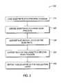
- FIG. 1illustrates an exemplary process sequence 100 for forming an improved tungsten-containing film according to one embodiment of the invention.
- a substrate to be processedis first loaded into a process chamber capable of performing cyclical deposition and the process conditions are adjusted (step 110 ). The substrate is then exposed to a soak process lasting in a range from about 1 second to about 90 seconds (step 120 ).
- a pulse of a tungsten-containing precursor accompanied with a suitable carrier gasis introduced into the processing chamber (step 130 ).
- a pulse of gasis then pulsed into the process chamber (step 140 ) to purge or otherwise remove any residual tungsten-containing precursor or by-products.
- a pulse of a reductant or reducing compound accompanied with a suitable carrier gasis introduced into the process chamber (step 150 ).
- the reducing gasmay be the same compound as the gas used for the soak process (step 120 ) or alternatively, the reducing gas may be a different compound, depending on the product throughput requirements and the device applications.
- a pulse of purge gasis then introduced into the processing chamber (step 160 ) to purge or otherwise remove any residual reducing compound.
- Suitable carrier gases or purge gasesinclude helium, argon, nitrogen, hydrogen, forming gas and combinations thereof.
- the borane compoundsutilize argon or nitrogen as a carrier gas and the silane compounds use hydrogen, argon or nitrogen as the carrier gas.
- a “pulse” as used hereinis intended to refer to a quantity of a particular compound that is intermittently or non-continuously introduced into a reaction zone of a processing chamber.
- the quantity of a particular compound within each pulsemay vary over time, depending on the duration of the pulse.
- the duration of each pulseis variable depending upon a number of factors such as, for example, the volume capacity of the process chamber employed, the vacuum system coupled thereto, and the volatility/reactivity of the particular compound itself.
- each deposition cycleforms a layer with a thickness in the range from about 1 ⁇ to about 10 ⁇ .
- subsequent deposition cyclesmay be needed to deposit tungsten nucleation layer having a desired thickness.
- a deposition cycle(steps 130 through 160 ) can be repeated until the desired thickness for the tungsten film is achieved.
- the nucleation layeris typically deposited to a thickness in a range from about 10 ⁇ to about 200 ⁇ . Thereafter, the process is stopped as indicated by step 180 when the desired thickness is achieved.
- Suitable tungsten-containing precursors or compoundsinclude tungsten hexafluoride (WF 6 ), tungsten hexachloride (WCl 6 ), tungsten carbonyl (W(CO) 6 ), bis(cyclopentadienyl)tungsten dichloride (Cp 2 WCl 2 ) and mesitylene tungsten tricarbonyl (C 9 H 12 W(CO) 3 ), as well as derivatives thereof.
- Suitable reducing compounds and soak compoundsinclude silane compounds, borane compounds, phosphine compounds, ammonia and ammine compounds and hydrogen.
- Silane compoundsinclude silane, disilane, trisilane, tetrasilane, chlorosilane, dichlorosilane, tetrachlorosilane, hexachlorodisilane and derivatives thereof, while borane compounds include borane, diborane, triborane, tetraborane, pentaborane, alkylboranes, such as triethylborane and derivatives thereof.
- the preferred reducing compounds and reductant for the soak processinclude silane, disilane, diborane, hydrogen and combinations thereof.
- the substrate surfacegenerally contains a barrier layer disposed thereon.
- the tungsten nucleation layeris deposited on the barrier layers.
- the substrate surfaceis exposed to a soak process at a temperature in the range from about 100° C. to about 600° C., preferably in the range from about 100° C. to about 500° C., more preferably in the range from about 300° C. to about 450° C.
- the temperature of the soak processis maintained for the subsequent vapor deposition process.
- the soak process (step 120 )is typically performed with the process chamber at a pressure in the range from about 1 Torr to about 150 Torr, preferably in the range from about 5 Torr to about 90 Torr. In some examples, a pressure is in a range from about 5 Torr to about 20 Torr.
- the pressureis about 40 Torr.
- the soak processis usually conducted to the substrate surface for a time period in the range from about 1 second to about 90 seconds. In one example, the soak process will last for about 60 seconds or less. In another example, the soak process will last for about 30 seconds or less. In another aspect, the soak process will last for about 10 seconds.
- the soak processincludes a soak compound, such as a reductant and usually has a carrier gas.
- the flow rate of the reductantis generally in the range from about 10 sccm to about 2,000 sccm, preferably in the range from about 50 sccm to about 500 sccm.
- the flow rate of the carrier gasis generally in the range from about 10 sccm to about 2,000 sccm, preferably in the range from about 50 sccm to about 500 sccm.
- the barrier layer disposed on the substrateis reduced and/or adsorbs the reductant to form a conditioned layer for the subsequent nucleation layer.
- the conditioned barrier layerprovides for a quicker and smoother deposition of the nucleation layer.
- diboraneis introduced with hydrogen, each having a flow rate in a range from about 50 sccm to about 500 sccm.
- the diborane and hydrogen gasesare introduced in a 1:1 volumetric ratio.
- silaneis introduced with hydrogen, each having a flow rate in a range from about 50 sccm to about 500 sccm.
- the reductant or soak compound utilized in the soak processis diborane or silane.
- the tungsten-containing precursoris preferably tungsten hexafluoride and introduced at a rate in the range from about 5 sccm to about 200 sccm.
- the tungsten-containing precursorcan be introduced with a carrier gas, such as argon with a flow rate in the range from about 50 sccm to about 1,000 sccm.
- the reductantis preferably diborane or silane and introduced at a rate in the range from about 5 sccm to about 2,000 sccm, preferably in the range from about 50 sccm to about 500 sccm.
- the reductantcan be introduced with a carrier gas, such as hydrogen, with a flow rate in the range from about 50 sccm to about 2,000 sccm.
- a purge gaspreferably argon or nitrogen
- steps 140 and 160are typically introduced at a rate from about 50 sccm to about 2,000 sccm, preferably at about 500 sccm.
- Steps 140 and 160may include a continuous flow of purge gas whereas the tungsten-containing compound and the reducing gas are pulsed into a steady stream of carrier gas.
- Each processing step (steps 130 through 160 )lasts from about 0.01 seconds to about 10 seconds, preferably in the range from about 0.1 seconds to about 1 second.
- tungsten depositionLonger processing steps, such as about 30 seconds or about 60 seconds, achieve tungsten deposition. However, the throughput is reduced. The specific pressures and times are obtained through experimentation. In one example, a 300 mm diameter wafer needs about twice the flow rate as a 200 mm diameter wafer in order to maintain similar throughput.
- An ALD process chamber used during embodiments described hereinis available from Applied Materials, Inc. located in Santa Clara, Calif. A more detailed description of an ALD process chamber may be found in commonly assigned U.S. patent application Ser. No. 10/032,284, entitled “Gas Delivery Apparatus and Method for Atomic Layer Deposition”, filed on Dec. 21, 2001, U.S. patent application Ser. No. 10/281,079, entitled “Gas Delivery Apparatus for Atomic Layer Deposition”, filed on Oct. 25, 2002, and U.S. patent application Ser. No. 10/016,300, entitled “Lid Assembly For A Processing System To Facilitate Sequential Deposition Techniques”, filed on Dec. 12, 2001, which are hereby incorporated by reference in their entirety.
- Software routinesare executed to initiate process recipes or sequences.
- the software routineswhen executed, transform the general purpose computer into a specific process computer that controls the chamber operation so that a chamber process is performed.
- software routinesmay be used to precisely control the activation of the electronic control valves for the execution of process sequences according to aspects of the invention.
- the software routinesmay be performed in hardware, as an application specific integrated circuit or other type of hardware implementation, or a combination of software or hardware.
- FIG. 2illustrates process 200 for the forming of a tungsten-containing material according to one embodiment described herein.
- the substrateis loaded into a process chamber.
- the substrateusually contains a barrier layer disposed thereon and is exposed to a first soak process during step 220 .
- the soak processincludes delivering a reducing gas containing a reductant into the process chamber.
- the substrate surfaceforms a treated layer, such as a reduced barrier layer.
- a nucleation layere.g., tungsten
- the nucleation layeris deposited by a vapor deposition process that includes ALD, CVD or pulsed-CVD.
- step 240the nucleation layer is exposed to a second soak process with the same or a different reductant as used in step 220 . Thereafter, a bulk layer (e.g., tungsten) is deposited on the nucleation layer during step 250 .
- the bulk layermay be deposited by a CVD process or a PVD process.
- the substrateis positioned into the process chamber.
- the substrate surfacemay contain a barrier layer disposed thereon.
- Barrier layersusually contain a metal or metal nitride material that includes titanium, titanium nitride, titanium silicon nitride, tantalum, tantalum nitride, tantalum silicon nitride, and combinations thereof.
- a barrier layermay be formed by process techniques such as chemical vapor deposition (CVD), atomic layer deposition (ALD), physical vapor deposition (PVD), derivatives thereof and combinations thereof.
- the barrier layeris usually deposited to a thickness of at least about 30 ⁇ , such as in a range from about 30 ⁇ to about 100 ⁇ .
- a barrier layeris deposited on the substrate surface by a CVD process by using tetrakis(dimethylamino)titanium (TDMAT) and ammonia.
- TDMATtetrakis(dimethylamino)titanium
- a barrier layeris deposited on the substrate surface by an ALD process by sequentially pulsing titanium tetrachloride (TiCl 4 ) and ammonia.
- a barrier layeris deposited on the substrate surface by a PVD process by sputtering from a titanium source in a nitrogen environment. The barrier layer may be plasma densified prior to performing a subsequent fabrication process.
- the process conditions, such as temperature and pressure, set during step 210may be used during step 220 .
- the process chamberis adjusted to heat the substrate at a temperature in the range from about 100° C. to about 600° C., preferably in the range from about 200° C. to about 500° C., and more preferably in the range from about 300° C. to about 450° C.
- the process chamberis maintained at a pressure in the range from about 1 Torr to about 150 Torr, preferably in the range from about 5 Torr to about 90 Torr.
- the process chamber used during the soak processmay be the same process chamber as used to deposit the barrier layer.
- the process chamber used during the soak processis used to deposit the subsequent nucleation layer during step 230 .
- the substrate surfaceis exposed to a soak process containing a reductant and an optional carrier gas.
- the reductantadsorbs and/or reacts to the substrate surface, namely the barrier layer, to form a treated surface.
- the treated surfaceprovides a quicker deposition process for an overall smooth and more uniform tungsten layer.
- the reductantsmay include silane compounds, borane compounds, phosphine compounds, ammonia and ammine compounds and hydrogen.
- Silane compoundsinclude silane, disilane, trisilane, tetrasilane, chlorosilane, dichlorosilane, tetrachlorosilane, hexachlorodisilane and derivatives thereof, while borane compounds include borane, diborane, triborane, tetraborane, pentaborane, alkylboranes, such as triethylborane and derivatives thereof.
- the preferred reductantsinclude silane, disilane, diborane and hydrogen.
- a carrier gasmay be co-flowed with the reductant.
- Carrier gasesinclude hydrogen, nitrogen, argon, helium and combinations thereof.
- diboraneis often used with a concentration of 5 vol % in argon or nitrogen.
- the soak process in step 220usually last for a period of time in the range from about 1 second to about 90 seconds.
- the barrier layer disposed on the substrateis reduced and/or adsorbs the reductant to form a conditioned layer for the subsequent nucleation layer.
- about 300 sccm of a 5 vol % diborane in argonis exposed to the substrate for about 30 seconds at about 15 Torr and about 350° C.
- about 200 sccm of a 5 vol % diborane in nitrogenis exposed to the substrate for about 24 seconds at about 90 Torr and about 400° C.
- a nucleation layeris deposited on the substrate surface, namely on the treated barrier layer.
- the nucleation layermay be deposited by a vapor deposition process that includes ALD, CVD and/or pulsed-CVD.
- the process chamber used to deposit the nucleation layermay be the same process chamber used in the soak processes as described in steps 220 and 240 .
- the nucleation layermay comprise tungsten, tungsten alloys, tungsten-containing materials (e.g., tungsten boride or tungsten silicide) and combinations thereof.
- the nucleation layeris typically deposited to a thickness in a range from about 10 ⁇ to about 200 ⁇ .
- an ALD process utilizing WF 6 and B 2 H 6deposits a nucleation layer with a thickness in a range from about 10 ⁇ to about 20 ⁇ , such as about 12 ⁇ .
- an ALD process utilizing WF 6 and SiH 4deposits a nucleation layer with a thickness in a range from about 10 ⁇ to about 50 ⁇ , such as about 30 ⁇ .
- a pulsed-CVD (e.g., co-flowed) processutilizing WF 6 and SiH 4 or WF 6 and B 2 H 6 deposits a nucleation layer with a thickness in a range from about 30 ⁇ to about 200 ⁇ , such as about 50 ⁇ .
- the ALD process as described herein during process 100may be used to deposit the nucleation layer.
- the substrate surfaceis exposed to a post soak process or a second soak process containing a reductant and an optional carrier gas.
- the reductantadsorbs and/or reacts to the substrate surface, namely the nucleation layer, to form a treated surface.
- the reductantsmay also include silane compounds, borane compounds, phosphine compounds, ammonia and ammine compounds and hydrogen.
- the preferred reductantsinclude silane, disilane, diborane and hydrogen.
- a carrier gasmay be co-flowed with the reductant and include hydrogen, nitrogen, argon, helium and combinations thereof.
- diboraneis often used with a concentration of 5 vol % in argon or nitrogen.
- the soak process in step 240usually last for a period of time in the range from about 1 second to about 90 seconds.
- the process chamberis adjusted to heat the substrate at a temperature in the range from about 100° C. to about 600° C., preferably in the range from about 200° C. to about 500° C., more preferably in the range from about 300° C. to about 450° C.
- the process chamberis maintained at a pressure in the range from about 1 Torr to about 150 Torr, preferably in the range from about 5 Torr to about 90 Torr.
- the barrier layer disposed on the substrateis reduced and/or adsorbs the reductant to form a conditioned layer for the subsequent bulk layer.
- about 300 sccm of a 5 vol % diborane in nitrogenis exposed to the substrate for about 30 seconds at about 30 Torr and about 300° C.
- about 200 sccm of a 5 vol % diborane in argonis exposed to the substrate for about 30 seconds at about 15 Torr and about 400° C.
- about 300 sccm of a 5 vol % diborane in argonis exposed to the substrate for about 10 seconds at about 90 Torr and about 400° C.
- a bulk layeris deposited on the substrate surface, namely on the treated nucleation layer.
- the bulk layermay be deposited by a vapor deposition process that includes CVD, pulsed-CVD and/or PVD.
- the process chamber used to deposit the bulk layermay be the same process chamber used in the post soak process as described in step 240 .
- the bulk layercomprises tungsten, tungsten alloys, tungsten-containing materials (e.g., tungsten boride, tungsten silicide or tungsten phosphide) and combinations thereof.
- the bulk layeris typically deposited to a thickness in the range from about 100 ⁇ to about 10,000 ⁇ , preferably from about 1,000 ⁇ to about 5,000 ⁇ .
- a CVD process utilizing WF 6 and B 2 H 6is used to deposit a bulk layer on the treated nucleation layer.
- a CVD process utilizing WF 6 and SiH 4is used to deposit a bulk layer on the treated nucleation layer.
- a PVD process utilizing a tungsten sourceis used to deposit a bulk layer on the treated nucleation layer. Processes for soaking a tungsten nucleation layer and depositing a tungsten bulk layer thereon is further described in the commonly assigned U.S. Pat. No. 6,156,382, which is incorporated by reference herein.
- a tungsten-containing filmis deposited by depositing more than one nucleation layer and may include multiple cycles of a vapor deposition process.
- the barrier layermay be exposed to a soak process prior to forming a first nucleation layer by a pulsed-CVD process.
- the process chamberis heated to a temperature in a range from about 400° C. to about 450° C., for example, about 425° C. and maintained at a pressure in a range from about 10 Torr to about 20 Torr, such as about 15 Torr.
- the pulsed-CVD processmay include exposing the substrate to a co-flow of a tungsten-containing compound and a reductant for a period of time from about 1 second to about 3 seconds, for example about 1.5 seconds.
- the flow of the reagentsinclude the tungsten-containing compound with a flow rate from about 30 sccm to about 90 sccm, such as about 60 sccm, while the reductant is at a flow rate from about 10 sccm to about 50 sccm, such as about 30 sccm.
- the co-flowis stopped and the process chamber purged.
- the reductantis pulsed into the chamber for a period of time from about 1 second to about 3 seconds, for example about 1 second.
- the reductantmay have a flow rate from about 10 sccm to about 50 sccm, such as about 30 sccm.
- the flow of the reductantis stopped and the chamber purged for about 0.5 seconds.
- the cycleis repeated until a predetermined thickness of the first nucleation layer is formed. For example, the process is repeated 3 times to form a layer with a thickness about 30 ⁇ .
- the preferred tungsten-containing compoundis tungsten hexafluoride and the preferred reductant is silane and/or diborane.
- the reductantis optionally used during a soak process prior or subsequent the deposition of the first nucleation layer.
- a second nucleation layermay be formed on the first nucleation layer.
- the process chambermay be kept at the same temperature, but the pressure of the process chamber is usually increased.
- the process chamberis maintained at a temperature in a range from about 400° C. to about 450° C., for example, about 425° C. and the a pressure is in a range from about 20 Torr to about 50 Torr, such as about 30 Torr.
- the CVD processmay include exposing the substrate to a co-flow of a tungsten-containing compound and a reductant for a period of time from about 4 seconds to about 8 seconds, for example about 6 seconds.
- the flow of the reagentsinclude the tungsten-containing compound with a flow rate from about 30 sccm to about 70 sccm, such as about 50 sccm, while the reductant has a flow rate from about 10 sccm to about 50 sccm, such as about 25 sccm.
- a second nucleation layeris deposited on the first nucleation layer and has a thickness in a range from about 50 ⁇ to about 1,000 ⁇ , preferably from about 150 ⁇ to about 300 ⁇ .
- the preferred tungsten-containing compoundis tungsten hexafluoride and the preferred reductant is silane and/or diborane.
- the reductantis optionally used during a soak process prior or subsequent the deposition of the second nucleation layer.
- a bulk layermay be deposited on the second nucleation layer.
- the bulk layermay be deposited by a tradition CVD process.
- the process chamberis maintained at a temperature in a range from about 400° C. to about 450° C., for example, about 425° C. and the pressure is maintained in a range from about 100 Torr to about 350 Torr, such as about 200 Torr.
- the flow of the reagentsinclude the tungsten-containing compound with a flow rate from about 200 sccm to about 800 sccm, such as about 400 sccm, while the reductant has a flow rate from about 2,000 sccm to about 8,000 sccm, such as about 4,000 sccm.
- the preferred tungsten-containing compoundis tungsten hexafluoride and the preferred reductant is hydrogen.
- a tungsten nucleation layer as described abovehas shown particular utility when integrated with traditional bulk fill techniques to form features with excellent film properties.
- An integration schemecan include ALD or pulsed-CVD processes to deposit a nucleation layer while a bulk layer may be deposited by CVD or PVD processes.
- Integrated processing systems capable of performing such an integration schemeinclude an Endura®, Endura SL®, Centura® and Producer® processing systems, each available from Applied Materials, Inc. located in Santa Clara, Calif. Any of these systems can be configured to include at least one ALD or pulsed-CVD chamber for depositing the nucleation layer and at least one CVD chamber or PVD chamber for bulk fill.
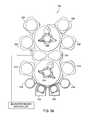
- FIG. 3Ais a schematic top-view diagram of an exemplary multi-chamber processing system 300 .
- the system 300generally includes load lock chambers 302 , 304 for the transfer of substrates into and out from the system 300 .
- the load lock chambers 302 , 304may “pump down” the substrates introduced into the system 300 .
- a first robot 310may transfer the substrates between the load lock chambers 302 , 304 , and a first set of one or more substrate processing chambers 312 , 314 , 316 , 318 (four are shown).
- Each processing chamber 312 , 314 , 316 , 318can be outfitted to perform a number of substrate processing operations such as cyclical layer deposition, CVD, PVD, etch, pre-clean, de-gas, orientation and other substrate processes.
- the first robot 310also transfers substrates to/from one or more transfer chambers 322 , 324 .
- the transfer chambers 322 , 324are used to maintain ultrahigh vacuum conditions while allowing substrates to be transferred within the system 300 .
- a second robot 330may transfer the substrates between the transfer chambers 322 , 324 and a second set of one or more processing chambers 332 , 334 , 336 , 338 .
- the processing chambers 332 , 334 , 336 , 338can be outfitted to perform a variety of substrate processing operations, such as cyclical deposition, CVD, PVD, etch, pre-clean, de-gas, and orientation, for example. Any of the substrate processing chambers 312 , 314 , 316 , 318 , 332 , 334 , 336 , 338 may be removed from the system 300 if not necessary for a particular process to be performed by the system 300 .
- each processing chamber 332 and 338may be a cyclical deposition chamber adapted to deposit a nucleation layer; each processing chamber 334 and 336 may be a cyclical deposition chamber, a chemical vapor deposition chamber or a physical vapor deposition chamber adapted to form a bulk layer; each processing chamber 312 and 314 may be a physical vapor deposition chamber, a chemical vapor deposition chamber, or a cyclical deposition chamber adapted to deposit a dielectric layer; and each processing chamber 316 and 318 may be an etch chamber outfitted to etch apertures or openings for interconnect features.
- This one particular arrangement of the system 300is provided to illustrate the invention and should not be used to limit the scope of the invention.
- Another integrated systemmay include nucleation deposition as well as bulk fill deposition in a single chamber.
- a chamberconfigured to operate in both a cyclical deposition mode as well as a conventional CVD mode can be used.
- One example of such a chamberis described in commonly assigned U.S. patent application Ser. No. 10/016,300, filed on Dec. 12, 2001, which is incorporated herein by reference.
- one or more cyclical deposition nucleation chambersare integrated onto a first processing system while one or more bulk layer deposition chambers are integrated onto a second processing system.
- substratesare first processed in the first system where a nucleation layer is deposited on a substrate. Thereafter, the substrates are moved to the second processing system where bulk deposition occurs.
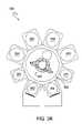
- FIG. 3Bis a schematic top-view diagram of an exemplary multi-chamber processing system 350 .
- the system 350generally includes load lock chambers 352 , 354 for the transfer of substrates into and out from the system 350 .
- the load lock chambers 352 , 354may “pump down” the substrates introduced into the system 350 .
- a robot 360may transfer the substrates between the load lock chambers 352 , 354 , and substrate processing chambers 362 , 364 , 366 , 368 , 370 and 372 .
- Each processing chamber 362 , 364 , 366 , 368 , 370 and 372can be outfitted to perform a number of substrate processing operations such as cyclical layer deposition, CVD, PVD, etch, pre-clean, de-gas, heat, orientation and other substrate processes.
- the robot 360also transfers substrates to/from a transfer chamber 356 . Any of the substrate processing chambers 362 , 364 , 366 , 368 , 370 and 372 may be removed from the system 350 if not necessary for a particular process to be performed by the system 350 .
- each processing chamber 364 and 370may be a cyclical deposition chamber adapted to deposit a nucleation layer; each processing chamber 366 and 368 may be a cyclical deposition chamber, a chemical vapor deposition chamber or a physical vapor deposition chamber adapted to form a bulk fill deposition layer.
- This one particular arrangement of the system 350is provided to illustrate the invention and should not be used to limit the scope of the invention.
- a carousel type batch processing system having a plurality of stations in a single chambercan be adapted to incorporate nucleation and bulk layer deposition into a single processing system.
- a purge gas curtainsuch as an argon gas curtain
- the substratesare loaded into the system sequentially and then rotated through each station and processed at least partially at each station.
- a substratemay be exposed to a cyclical deposition nucleation step at a first station and then to partial bulk fill CVD steps at each of the subsequent stations.
- nucleationmay occur at more than one station and bulk fill may occur at one or more stations.
- the nucleation layer and the bulk layermay be deposited in separate carousel type systems.
- the soak and the nucleation stepsare completed in one carousel while the bulk steps are done on another carousel, wherein both carousels are part of the same process system.
- Each platencan be temperature controlled to provide at least some process control at each station.
- the process pressuretypically remains the same between stations because the stations are housed in a single chamber. Some pressure control may be available in a micro or mini environment present at each station due to the inert gas curtain.
- the nucleation layeris typically deposited to a thickness in a range from about 10 ⁇ to about 200 ⁇ and the bulk layer has a thickness in a range from about 100 ⁇ to about 10,000 ⁇ , preferably in the range from about 1,000 ⁇ to about 5,000 ⁇ .
- the thickness of these filmscan vary depending on the feature sizes and aspect ratios of a given application. Accordingly, the films are suitably sized to accommodate the geometries of a given application.
- the followingare some exemplary geometries and applications that can benefit from a nucleation layer deposited according to embodiments described herein. The following descriptions are intended for illustrative purposes only, and are not intended to limit the uses of the present invention.
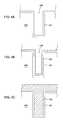
- FIGS. 4A-Cshow cross sectional views of a semiconductor feature that one embodiment of the process is utilized to fill a via 460 .
- the substrate 450includes at least one via 460 .
- a barrier layer 451such as titanium nitride, is deposited by ALD, CVD or PVD techniques to the substrate 450 with via 460 .
- a soak processis administered to barrier layer 451 prior to the nucleation of a tungsten layer 452 , as depicted in FIG. 4B .
- the soak processrenders the sidewalls, of the barrier layer 451 within the via 460 , to adhere and grow the tungsten layer 452 at about the same rate as the barrier layer 451 outside the via 460 .
- tungsten layer 452 on the sidewallsis not constant with respect to the growth of tungsten layer 452 outside the via 460 .
- a secondary soak or post soak processis conducted to treat tungsten layer 452 .
- the post soak processprovides tungsten layer 452 to more smoothly continue growth while filling the via 460 , as demonstrated in FIG. 4C .
- an ALD processis continued after deposition of a tungsten nucleation layer to deposit the tungsten bulk layer.
- an ALD processis used to deposit the tungsten nucleation layer and a CVD process is used to deposit the tungsten bulk layer.
- an ALD processis used to deposit the tungsten nucleation layer and a PVD process is used to deposit the tungsten bulk layer.
- a pulsed-CVD processis used to deposit the tungsten nucleation layer and a conventional CVD process is used to deposit the tungsten bulk layer.
- a pulsed-CVD processis used to deposit the tungsten nucleation layer and a PVD process is used to deposit the tungsten bulk layer.
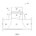
- FIG. 5shows a cross sectional view of an exemplary metal oxide gate device 400 utilizing a nucleation layer deposited according to embodiments described herein.
- the device 400generally includes an exposed gate 410 surrounded by spacers 416 and silicon source/drain areas 420 formed within a substrate surface 412 .
- the spacers 416typically include an oxide, such as silicon dioxide, or a nitride, such as silicon nitride.
- the metal gate 410includes an oxide layer 411 , a polysilicon layer 414 , a titanium nitride barrier layer 415 and a tungsten layer 422 .
- the oxide layer 411separates the substrate 412 from the polysilicon layer 414 .
- the oxide layer 411 and the polysilicon layer 414are deposited using conventional deposition techniques.
- the titanium nitride barrier layer 415is deposited on the polysilicon layer 414 .
- the titanium nitride barrier layer 415may be a bi-layer stack formed by depositing a PVD titanium layer followed by a CVD titanium nitride layer.
- the titanium nitride barrier layer 415may also be deposited using a cyclical deposition technique, such as the process shown and described in commonly assigned and co-pending U.S. patent application Ser. No. 10/032,293, filed on Dec. 21, 2001, entitled “Chamber Hardware Design for Titanium Nitride Atomic Layer Deposition,” published as U.S. Patent Publication 20030116087, which is incorporated by reference herein.
- a soak processis administered to the substrate surface.
- the soakincludes a silane compound or a borane compound along with at least one carrier gas.
- a preferred silane compoundis silane, a preferred borane compound is diborane and a preferred carrier gas is either hydrogen, nitrogen and/or argon.
- silanehas a flow rate in the range from about 25 sccm to about 500 sccm and hydrogen has a flow rate in the range from about 200 sccm to about 700 sccm.
- the soak processis conducted at a temperature in the range from about 100° C.
- diboranehas a flow rate in the range from about 25 sccm to about 500 sccm and hydrogen and/or argon has a flow rate in the range from about 200 sccm to about 700 sccm.
- the soak processis conducted at a temperature in the range from about 100° C.
- a nucleation layer 417is then cyclically deposited over the barrier layer 415 following treatment of the substrate surface with a soak process.
- the nucleation layer 417is cyclically deposited using alternating pulses of tungsten hexafluoride and diborane.
- the tungsten hexafluorideis pulsed at a rate of between about 1 sccm and about 100 sccm, such as between about 5 sccm and about 50 sccm, for about 0.3 seconds.
- a carrier gassuch as argon, is provided along with the tungsten hexafluoride at a rate of about 100 sccm to about 1,000 sccm, such as between about 100 sccm to about 500 sccm.
- the diboraneis pulsed at a rate of about 50 sccm and about 1,000 sccm, such as between about 400 sccm and about 600 sccm, for about 0.3 seconds.
- a carrier gas, such as hydrogenis provided along with the diborane at a rate between about 50 sccm to about 500 sccm, such as between about 100 sccm to about 300 sccm.
- the substrateis maintained at a temperature between about 100° C.
- argonis pulsed for about 0.5 seconds to purge or otherwise remove any reactive compounds from the processing chamber.
- the nucleation layer 417is cyclically deposited using alternating pulses of tungsten hexafluoride and silane.
- the tungsten hexafluorideis pulsed as described above with argon for about 0.5 seconds.
- the silaneis pulsed at a rate of about 1 sccm to about 100 sccm, such as between about 5 sccm to about 50 sccm, for about 0.5 seconds.
- a carrier gas, such as hydrogen,is provided along with the silane at a rate of about 100 sccm and about 1,000 sccm, such as between about 100 sccm and about 500 sccm.
- Argonis pulsed at a rate of about 100 sccm to about 1,000 sccm, such as between about 300 sccm to about 700 sccm, for about 0.5 seconds between the pulses of the tungsten hexafluoride and the pulses of silane.
- the substrateis maintained at a temperature between about 100° C. and about 400° C., preferably at about 300° C., at a chamber pressure between about 1 Torr and about 30 Torr.
- a nucleation layer 417is deposited by a pulsed-CVD process on the barrier layer 415 following treatment of the substrate surface with a soak process.
- the pulsed-CVD processincludes co-flowing WF 6 and B 2 H 6 or WF 6 and SiH 4 at a temperature in a range from about 300° C. to about 500° C., preferably from about 400° C. to about 450° C.
- the pulsed-CVD processpulses the co-flowing precursors at a time period from about 0.5 seconds to about 3 seconds, preferably about 1.5.
- a second soak process or post soak processis administered to the substrate surface.
- the soak processincludes a reductant, such as silane compound or a borane compound along with at least one carrier gas.
- the reductantis diborane and a preferred carrier gas is hydrogen, nitrogen and/or argon.
- a reducing gas containing 5 vol % of diborane in argonhas a flow rate in the range from about 100 sccm to about 500 sccm, preferably about 300 sccm.
- the soak processis conducted at a temperature in the range from about 100° C.
- a nucleation layer formed utilizing soak processeshas advantages over a nucleation layer formed without the soak processes.
- the tungsten filmshows less stress for the integrated film, as well as, less fluorine content at the interface of the nucleation layer.
- the nucleation layer deposited post a soak treatmenthas higher uniformity coverage and is deposited quicker due to a reduced incubation period.
- a tungsten bulk fill 422is then deposited on the treated tungsten nucleation layer 417 .
- the tungsten bulk fill 422may be deposited by alternately adsorbing a tungsten-containing compound and a reducing compound as described above.
- a more detailed description of tungsten deposition using a cyclical deposition techniquemay be found in commonly assigned U.S. patent application Ser. No. 10/016,300, entitled “Lid Assembly For A Processing System To Facilitate Sequential Deposition Techniques,” filed on Dec. 12, 2001 and in commonly assigned U.S. patent application Ser. No.
- the top portion of the resulting structure 400may be planarized.
- a chemical mechanical polishing (CMP) apparatusmay be used, such as the MirraTM System available from Applied Materials, Santa Clara, Calif., for example.
- Portions of the tungsten bulk fill 422are removed from the top of the structure leaving a fully planar surface.
- the intermediate surfaces of the structuremay be planarized between the depositions of the subsequent layers described above.
- FIG. 6is a cross sectional view of a conventional DRAM device having a transistor 520 positioned adjacent a top portion of a trench capacitor 530 .
- the access transistor 520 for the DRAM device 510is positioned adjacent a top portion of the trench capacitor 530 .
- the access transistor 520comprises an n-p-n transistor having a source region 522 , a gate region 524 and a drain region 526 .
- the gate region 524is a P ⁇ doped silicon epi-layer disposed over the P+ substrate.
- the source region 522 of the access transistor 520is an N+ doped material disposed on a first side of the gate region 524 and the drain region 526 is an N+ doped material disposed on a second side of the gate region 524 , opposite the source region 522 .
- the source and drain regions 522 , 524may be connected to a tungsten plug 560 .
- Each tungsten plug 560includes a titanium liner 562 , a tungsten nucleation layer 564 , and a bulk tungsten fill 566 .
- the titanium liner 562may be a bi-layer stack comprising PVD titanium followed by CVD titanium nitride.
- the titanium liner 562may be a bi-layer stack comprising ALD deposited titanium followed by ALD deposited titanium nitride.
- the tungsten nucleation layer 564is formed by using a soak process and an ALD process or a soak process and a pulsed-CVD process as described above.
- the tungsten bulk fill 566may be deposited using a post soak process and any conventional deposition techniques, including ALD, CVD and PVD.
- the trench capacitor 530generally includes a first electrode 532 , a second electrode 534 and a dielectric material 536 disposed therebetween.
- the P+ substrateserves as a first electrode 532 of the trench capacitor 530 and is connected to a ground connection 541 .
- a trench 538is formed in the P+ substrate and filled with a heavily doped N+ polysilicon that serves as the second electrode 534 of the trench capacitor 530 .
- the dielectric material 536is disposed between the first electrode 532 (i.e., P+ substrate) and the second electrode 534 (i.e., N+ polysilicon).
- the trench capacitor 530also includes a first tungsten nitride barrier layer 540 disposed between the dielectric material 536 and the first electrode 532 .
- a second tungsten nitride barrier layer 542is disposed between the dielectric material 536 and the second electrode 534 .
- the barrier layers 540 , 542are a combination film, such as W/WN.
- DRAM deviceutilizes an n-p-n transistor, a P+ substrate as a first electrode, and an N+ polysilicon as a second electrode of the capacitor
- transistor designs and electrode materialsare contemplated by the present invention to form DRAM devices.
- other devices, such as crown capacitors for example,are contemplated by the present invention.
- the following exampleswere conducted to substrates that contained a barrier layer deposited on the surface.
- the barrier layerwas formed by first depositing a titanium layer by a PVD process on a 300 mm substrate surface to a thickness of about 20 ⁇ . Subsequently, a titanium nitride layer was deposited on the titanium layer using a CVD process of co-flowing PDMAT and ammonia. The tantalum nitride layer was deposited to a thickness of about 80 ⁇ .
- the substratewas placed into an ALD chamber and exposed to a soak process under the following conditions:
- Durationabout 30 seconds.
- tungsten nucleation layerwas formed on the barrier layer in the same ALD chamber from the previous soak process using an ALD process under the following conditions:
- the cyclewas repeated 4 times to form a nucleation layer with a thickness of about 12 ⁇ . Thereafter, the substrate was maintained in the ALD chamber and exposed to a second soak process under the following conditions:
- Durationabout 30 seconds.
- the substratewas transferred into a CVD chamber and a bulk tungsten layer was deposited to a thickness of about 2,500 ⁇ on the nucleation layer using a CVD process at about 400° C.
- the resulting tungsten bulk fill filmexhibited a uniformity variance of less than about 2 percent.
- the substratewas placed into an ALD chamber and exposed to a soak process under the following conditions:
- Durationabout 30 seconds.
- tungsten nucleation layerwas formed on the barrier layer in the same ALD chamber as used in the prior soak process using an ALD process under the following conditions:
- the cyclewas repeated 4 times to form a nucleation layer with a thickness of about 30 ⁇ . Thereafter, the substrate was transferred to a CVD chamber and exposed to a second soak process under the following conditions:
- Durationabout 30 seconds.
- the substratewas maintained in the CVD chamber and a bulk tungsten layer was deposited to a thickness of about 2,500 ⁇ on the nucleation layer using a CVD process at about 400° C.
- the resulting tungsten bulk fill filmexhibited a uniformity variance of less than about 4 percent.
- the substratewas placed into a CVD chamber and exposed to a soak process under the following conditions:
- Durationabout 24 seconds.
- tungsten nucleation layerwas formed on the barrier layer in the CVD chamber from the previous soak process using a pulsed-CVD process under the following conditions:
- Pulse duration1.5 seconds
- the pulsed-CVD processwas continued until the nucleation layer had a thickness of about 50 ⁇ . Thereafter, the substrate was kept in the CVD chamber and a second nucleation layer was deposited on the first nucleation layer.
- the second nucleation layerwas deposited by a traditional CVD process to a thickness of about 200 ⁇ under the following conditions:
- a bulk tungsten layerwas deposited to a thickness of about 2,500 ⁇ on the second nucleation layer using a CVD process at about 400° C.
- the substratewas placed into a CVD chamber and exposed to a soak process under the following conditions:
- Durationabout 24 seconds.
- tungsten nucleation layerwas formed on the barrier layer in the previously used CVD chamber using a pulsed-CVD process under the following conditions:
- Pulse duration1.5 seconds
- the pulsed-CVD processwas continued until the nucleation layer had a thickness of about 50 ⁇ . Thereafter, the substrate was kept in the CVD chamber and a second nucleation layer was deposited on the first nucleation layer.
- the second nucleation layerwas deposited by a traditional CVD process to a thickness of about 200 ⁇ under the following conditions:
- the substratewas placed into a CVD chamber and exposed to a soak process under the following conditions:
- Durationabout 24 seconds.
- tungsten nucleation layerwas formed on the barrier layer in the same CVD chamber used during the soak process using a pulsed-CVD process under the following conditions:
- Pulse duration1.5 seconds
- the pulsed-CVD processwas continued until the nucleation layer had a thickness of about 150 ⁇ . Thereafter, the substrate was kept in the CVD chamber and exposed to a second soak process under the following conditions:
- Durationabout 30 seconds.
- the substratewas maintained in the CVD chamber and a bulk tungsten layer was deposited to a thickness of about 2,500 ⁇ on the nucleation layer using a CVD process at about 400° C.
- the resulting tungsten bulk fill filmexhibited a uniformity variance of less than about 4 percent.
- the substratewas placed into a CVD chamber and exposed to a soak process under the following conditions:
- Durationabout 24 seconds.
- tungsten nucleation layerwas formed on the barrier layer in the CVD chamber used during the prior soak process using a pulsed-CVD process under the following conditions:
- Pulse duration1.5 seconds
- the pulsed-CVD processwas continued until the nucleation layer had a thickness of about 150 ⁇ . Thereafter, the substrate was kept in the CVD chamber and exposed to a second soak process under the following conditions:
- Durationabout 10 seconds.
- the substratewas maintained in the CVD chamber and a bulk tungsten layer was deposited to a thickness of about 2,500 ⁇ on the nucleation layer using a CVD process at about 400° C.
- the resulting tungsten bulk fill filmexhibited a uniformity variance of less than about 2 percent.
- the substratewas placed into a CVD chamber and exposed to a soak process under the following conditions:
- Durationabout 1 second.
- the soak processis stopped for 0.5 seconds, the chamber purged and then a tungsten nucleation layer was formed on the barrier layer in the CVD chamber used during the prior soak process using a pulsed-CVD process under the following conditions:
- Pulse duration1.5 seconds
- the first nucleation processwas stopped and the chamber purged for about 0.5 seconds. Then the soak process and the pulsed-CVD process were repeated in a cycle for three times to form a first nucleation layer with a thickness of about 50 ⁇ . Thereafter, the substrate was kept in the CVD chamber and exposed to a traditional CVD process to form a second nucleation layer with a thickness of about 200 ⁇ on the first nucleation layer under the following conditions:
- the substratewas maintained in the CVD chamber and a bulk tungsten layer was deposited to a thickness of about 2,500 ⁇ on the second nucleation layer using a CVD process under the following conditions:
- Pulse duration30 seconds.
Landscapes
- Engineering & Computer Science (AREA)
- Chemical & Material Sciences (AREA)
- Power Engineering (AREA)
- Physics & Mathematics (AREA)
- Computer Hardware Design (AREA)
- Condensed Matter Physics & Semiconductors (AREA)
- General Physics & Mathematics (AREA)
- Manufacturing & Machinery (AREA)
- Microelectronics & Electronic Packaging (AREA)
- General Chemical & Material Sciences (AREA)
- Chemical Kinetics & Catalysis (AREA)
- Metallurgy (AREA)
- Materials Engineering (AREA)
- Mechanical Engineering (AREA)
- Organic Chemistry (AREA)
- Plasma & Fusion (AREA)
- Chemical Vapour Deposition (AREA)
- Electrodes Of Semiconductors (AREA)
- Internal Circuitry In Semiconductor Integrated Circuit Devices (AREA)
Abstract
Description
- pulse A: 20 sccm WF6and 300 sccm Ar;
- pulse B: 150 sccm B2H6and 150 sccm H2;
- Ar-purge: 500 sccm;
- pulse A: 0.2 seconds;
- Ar-purge: 0.5 seconds; and
- pulse B: 0.2 seconds.
- pulse A: 30 sccm WF6and 300 sccm Ar;
- pulse B: 20 sccm SiH4and 300 sccm H2;
- Ar purge: 500 sccm;
- Ar-purge: 0.5 seconds;
- pulse A: 0.3 seconds;
- Ar-purge: 0.5 seconds; and
- pulse B: 0.3 seconds.
Claims (15)
Priority Applications (1)
| Application Number | Priority Date | Filing Date | Title |
|---|---|---|---|
| US12/179,002US7745333B2 (en) | 2000-06-28 | 2008-07-24 | Methods for depositing tungsten layers employing atomic layer deposition techniques |
Applications Claiming Priority (11)
| Application Number | Priority Date | Filing Date | Title |
|---|---|---|---|
| US09/605,593US6551929B1 (en) | 2000-06-28 | 2000-06-28 | Bifurcated deposition process for depositing refractory metal layers employing atomic layer deposition and chemical vapor deposition techniques |
| US09/678,266US7101795B1 (en) | 2000-06-28 | 2000-10-03 | Method and apparatus for depositing refractory metal layers employing sequential deposition techniques to form a nucleation layer |
| US30576501P | 2001-07-16 | 2001-07-16 | |
| US32845101P | 2001-10-10 | 2001-10-10 | |
| US10/196,514US6936538B2 (en) | 2001-07-16 | 2002-07-15 | Method and apparatus for depositing tungsten after surface treatment to improve film characteristics |
| US10/268,195US6797340B2 (en) | 2001-10-10 | 2002-10-10 | Method for depositing refractory metal layers employing sequential deposition techniques |
| US10/418,728US20060040052A1 (en) | 2001-10-10 | 2003-04-18 | Methods for depositing tungsten layers employing atomic layer deposition techniques |
| US10/762,764US20040209465A1 (en) | 2000-06-28 | 2004-01-22 | Method and apparatus for depositing refractory metal layers employing sequential deposition techniques to form a nucleation layer |
| US10/879,448US20040247788A1 (en) | 2001-10-10 | 2004-06-29 | Method for depositing refractory metal layers employing sequential deposition techniques |
| US11/038,592US7405158B2 (en) | 2000-06-28 | 2005-01-19 | Methods for depositing tungsten layers employing atomic layer deposition techniques |
| US12/179,002US7745333B2 (en) | 2000-06-28 | 2008-07-24 | Methods for depositing tungsten layers employing atomic layer deposition techniques |
Related Parent Applications (1)
| Application Number | Title | Priority Date | Filing Date |
|---|---|---|---|
| US11/038,592ContinuationUS7405158B2 (en) | 2000-06-28 | 2005-01-19 | Methods for depositing tungsten layers employing atomic layer deposition techniques |
Publications (2)
| Publication Number | Publication Date |
|---|---|
| US20080280438A1 US20080280438A1 (en) | 2008-11-13 |
| US7745333B2true US7745333B2 (en) | 2010-06-29 |
Family
ID=36692850
Family Applications (2)
| Application Number | Title | Priority Date | Filing Date |
|---|---|---|---|
| US11/038,592Expired - LifetimeUS7405158B2 (en) | 2000-06-28 | 2005-01-19 | Methods for depositing tungsten layers employing atomic layer deposition techniques |
| US12/179,002Expired - Fee RelatedUS7745333B2 (en) | 2000-06-28 | 2008-07-24 | Methods for depositing tungsten layers employing atomic layer deposition techniques |
Family Applications Before (1)
| Application Number | Title | Priority Date | Filing Date |
|---|---|---|---|
| US11/038,592Expired - LifetimeUS7405158B2 (en) | 2000-06-28 | 2005-01-19 | Methods for depositing tungsten layers employing atomic layer deposition techniques |
Country Status (3)
| Country | Link |
|---|---|
| US (2) | US7405158B2 (en) |
| TW (1) | TWI428469B (en) |
| WO (1) | WO2006078779A2 (en) |
Cited By (32)
| Publication number | Priority date | Publication date | Assignee | Title |
|---|---|---|---|---|
| US20090004848A1 (en)* | 2007-06-28 | 2009-01-01 | Choon Hwan Kim | Method for fabricating interconnection in semiconductor device |
| US20100267235A1 (en)* | 2009-04-16 | 2010-10-21 | Feng Chen | Methods for depositing ultra thin low resistivity tungsten film for small critical dimension contacts and interconnects |
| US8853080B2 (en) | 2012-09-09 | 2014-10-07 | Novellus Systems, Inc. | Method for depositing tungsten film with low roughness and low resistivity |
| US8859417B2 (en) | 2013-01-03 | 2014-10-14 | Globalfoundries Inc. | Gate electrode(s) and contact structure(s), and methods of fabrication thereof |
| US9076843B2 (en) | 2001-05-22 | 2015-07-07 | Novellus Systems, Inc. | Method for producing ultra-thin tungsten layers with improved step coverage |
| US9153486B2 (en) | 2013-04-12 | 2015-10-06 | Lam Research Corporation | CVD based metal/semiconductor OHMIC contact for high volume manufacturing applications |
| US9159571B2 (en) | 2009-04-16 | 2015-10-13 | Lam Research Corporation | Tungsten deposition process using germanium-containing reducing agent |
| US9230815B2 (en) | 2012-10-26 | 2016-01-05 | Appled Materials, Inc. | Methods for depositing fluorine/carbon-free conformal tungsten |
| US9240347B2 (en) | 2012-03-27 | 2016-01-19 | Novellus Systems, Inc. | Tungsten feature fill |
| US9589808B2 (en) | 2013-12-19 | 2017-03-07 | Lam Research Corporation | Method for depositing extremely low resistivity tungsten |
| US9613818B2 (en) | 2015-05-27 | 2017-04-04 | Lam Research Corporation | Deposition of low fluorine tungsten by sequential CVD process |
| US9637395B2 (en) | 2012-09-28 | 2017-05-02 | Entegris, Inc. | Fluorine free tungsten ALD/CVD process |
| US9741817B2 (en)* | 2016-01-21 | 2017-08-22 | Tower Semiconductor Ltd. | Method for manufacturing a trench metal insulator metal capacitor |
| US9754824B2 (en) | 2015-05-27 | 2017-09-05 | Lam Research Corporation | Tungsten films having low fluorine content |
| US20170309490A1 (en)* | 2014-09-24 | 2017-10-26 | Hitachi Kokusai Electric Inc. | Method of manufacturing semiconductor device |
| US9953984B2 (en) | 2015-02-11 | 2018-04-24 | Lam Research Corporation | Tungsten for wordline applications |
| US9978605B2 (en) | 2015-05-27 | 2018-05-22 | Lam Research Corporation | Method of forming low resistivity fluorine free tungsten film without nucleation |
| US9997405B2 (en) | 2014-09-30 | 2018-06-12 | Lam Research Corporation | Feature fill with nucleation inhibition |
| US10256142B2 (en) | 2009-08-04 | 2019-04-09 | Novellus Systems, Inc. | Tungsten feature fill with nucleation inhibition |
| US10636705B1 (en) | 2018-11-29 | 2020-04-28 | Applied Materials, Inc. | High pressure annealing of metal gate structures |
| US11043386B2 (en) | 2012-10-26 | 2021-06-22 | Applied Materials, Inc. | Enhanced spatial ALD of metals through controlled precursor mixing |
| US11348795B2 (en) | 2017-08-14 | 2022-05-31 | Lam Research Corporation | Metal fill process for three-dimensional vertical NAND wordline |
| US11549175B2 (en) | 2018-05-03 | 2023-01-10 | Lam Research Corporation | Method of depositing tungsten and other metals in 3D NAND structures |
| US11705337B2 (en) | 2017-05-25 | 2023-07-18 | Applied Materials, Inc. | Tungsten defluorination by high pressure treatment |
| US11939668B2 (en) | 2022-04-26 | 2024-03-26 | Applied Materials, Inc. | Gas delivery for tungsten-containing layer |
| US11972952B2 (en) | 2018-12-14 | 2024-04-30 | Lam Research Corporation | Atomic layer deposition on 3D NAND structures |
| US12002679B2 (en) | 2019-04-11 | 2024-06-04 | Lam Research Corporation | High step coverage tungsten deposition |
| US12077858B2 (en) | 2019-08-12 | 2024-09-03 | Lam Research Corporation | Tungsten deposition |
| US12237221B2 (en) | 2019-05-22 | 2025-02-25 | Lam Research Corporation | Nucleation-free tungsten deposition |
| TWI890939B (en)* | 2021-04-02 | 2025-07-21 | 美商應用材料股份有限公司 | Nucleation layers for growth of gallium-and-nitrogen-containing regions |
| EP4334490A4 (en)* | 2021-05-07 | 2025-08-06 | Entegris Inc | PROCESS FOR DEPOSITING MOLYBDENUM OR TUNGSTEN MATERIALS |
| US12444651B2 (en) | 2022-06-28 | 2025-10-14 | Novellus Systems, Inc. | Tungsten feature fill with nucleation inhibition |
Families Citing this family (122)
| Publication number | Priority date | Publication date | Assignee | Title |
|---|---|---|---|---|
| US6974766B1 (en)* | 1998-10-01 | 2005-12-13 | Applied Materials, Inc. | In situ deposition of a low κ dielectric layer, barrier layer, etch stop, and anti-reflective coating for damascene application |
| US6620723B1 (en) | 2000-06-27 | 2003-09-16 | Applied Materials, Inc. | Formation of boride barrier layers using chemisorption techniques |
| US7101795B1 (en) | 2000-06-28 | 2006-09-05 | Applied Materials, Inc. | Method and apparatus for depositing refractory metal layers employing sequential deposition techniques to form a nucleation layer |
| US6551929B1 (en)* | 2000-06-28 | 2003-04-22 | Applied Materials, Inc. | Bifurcated deposition process for depositing refractory metal layers employing atomic layer deposition and chemical vapor deposition techniques |
| US7732327B2 (en) | 2000-06-28 | 2010-06-08 | Applied Materials, Inc. | Vapor deposition of tungsten materials |
| US7964505B2 (en) | 2005-01-19 | 2011-06-21 | Applied Materials, Inc. | Atomic layer deposition of tungsten materials |
| US7405158B2 (en) | 2000-06-28 | 2008-07-29 | Applied Materials, Inc. | Methods for depositing tungsten layers employing atomic layer deposition techniques |
| US6936538B2 (en) | 2001-07-16 | 2005-08-30 | Applied Materials, Inc. | Method and apparatus for depositing tungsten after surface treatment to improve film characteristics |
| US7955972B2 (en) | 2001-05-22 | 2011-06-07 | Novellus Systems, Inc. | Methods for growing low-resistivity tungsten for high aspect ratio and small features |
| US7211144B2 (en)* | 2001-07-13 | 2007-05-01 | Applied Materials, Inc. | Pulsed nucleation deposition of tungsten layers |
| TW581822B (en) | 2001-07-16 | 2004-04-01 | Applied Materials Inc | Formation of composite tungsten films |
| US20030029715A1 (en)* | 2001-07-25 | 2003-02-13 | Applied Materials, Inc. | An Apparatus For Annealing Substrates In Physical Vapor Deposition Systems |
| US20030036242A1 (en)* | 2001-08-16 | 2003-02-20 | Haining Yang | Methods of forming metal-comprising materials and capacitor electrodes; and capacitor constructions |
| US6936906B2 (en)* | 2001-09-26 | 2005-08-30 | Applied Materials, Inc. | Integration of barrier layer and seed layer |
| US6833161B2 (en)* | 2002-02-26 | 2004-12-21 | Applied Materials, Inc. | Cyclical deposition of tungsten nitride for metal oxide gate electrode |
| US7279432B2 (en) | 2002-04-16 | 2007-10-09 | Applied Materials, Inc. | System and method for forming an integrated barrier layer |
| US7211508B2 (en) | 2003-06-18 | 2007-05-01 | Applied Materials, Inc. | Atomic layer deposition of tantalum based barrier materials |
| US7429402B2 (en)* | 2004-12-10 | 2008-09-30 | Applied Materials, Inc. | Ruthenium as an underlayer for tungsten film deposition |
| US7473637B2 (en)* | 2005-07-20 | 2009-01-06 | Micron Technology, Inc. | ALD formed titanium nitride films |
| US8993055B2 (en) | 2005-10-27 | 2015-03-31 | Asm International N.V. | Enhanced thin film deposition |
| TWI332532B (en)* | 2005-11-04 | 2010-11-01 | Applied Materials Inc | Apparatus and process for plasma-enhanced atomic layer deposition |
| KR100713925B1 (en)* | 2005-12-28 | 2007-05-07 | 주식회사 하이닉스반도체 | Manufacturing method of semiconductor device |
| TWI395335B (en)* | 2006-06-30 | 2013-05-01 | Applied Materials Inc | Formation of nanocrystals |
| KR100881391B1 (en)* | 2006-09-29 | 2009-02-05 | 주식회사 하이닉스반도체 | Gate Forming Method of Semiconductor Device |
| US7611751B2 (en) | 2006-11-01 | 2009-11-03 | Asm America, Inc. | Vapor deposition of metal carbide films |
| US7897495B2 (en)* | 2006-12-12 | 2011-03-01 | Applied Materials, Inc. | Formation of epitaxial layer containing silicon and carbon |
| US8821637B2 (en)* | 2007-01-29 | 2014-09-02 | Applied Materials, Inc. | Temperature controlled lid assembly for tungsten nitride deposition |
| US9064960B2 (en)* | 2007-01-31 | 2015-06-23 | Applied Materials, Inc. | Selective epitaxy process control |
| US7713874B2 (en)* | 2007-05-02 | 2010-05-11 | Asm America, Inc. | Periodic plasma annealing in an ALD-type process |
| US20080273410A1 (en)* | 2007-05-04 | 2008-11-06 | Jaydeb Goswami | Tungsten digitlines |
| KR100830590B1 (en)* | 2007-06-01 | 2008-05-21 | 삼성전자주식회사 | Tungsten film, method for forming the same, method for forming a semiconductor device and its semiconductor device including the same |
| US7655567B1 (en) | 2007-07-24 | 2010-02-02 | Novellus Systems, Inc. | Methods for improving uniformity and resistivity of thin tungsten films |
| WO2009042713A1 (en)* | 2007-09-28 | 2009-04-02 | Applied Materials, Inc. | Vapor deposition of tungsten materials |
| US7772114B2 (en)* | 2007-12-05 | 2010-08-10 | Novellus Systems, Inc. | Method for improving uniformity and adhesion of low resistivity tungsten film |
| US8053365B2 (en) | 2007-12-21 | 2011-11-08 | Novellus Systems, Inc. | Methods for forming all tungsten contacts and lines |
| US8062977B1 (en) | 2008-01-31 | 2011-11-22 | Novellus Systems, Inc. | Ternary tungsten-containing resistive thin films |
| KR101540077B1 (en)* | 2008-04-16 | 2015-07-28 | 에이에스엠 아메리카, 인코포레이티드 | Atomic layer deposition of metal carbide films using aluminum hydrocarbon compounds |
| US8058170B2 (en)* | 2008-06-12 | 2011-11-15 | Novellus Systems, Inc. | Method for depositing thin tungsten film with low resistivity and robust micro-adhesion characteristics |
| US8551885B2 (en) | 2008-08-29 | 2013-10-08 | Novellus Systems, Inc. | Method for reducing tungsten roughness and improving reflectivity |
| JP2010093116A (en)* | 2008-10-09 | 2010-04-22 | Panasonic Corp | Semiconductor device and method for manufacturing the same |
| WO2010077847A2 (en)* | 2008-12-31 | 2010-07-08 | Applied Materials, Inc. | Method of depositing tungsten film with reduced resistivity and improved surface morphology |
| JP2010199349A (en)* | 2009-02-26 | 2010-09-09 | Toshiba Corp | Method for fabricating semiconductor device |
| US20100276764A1 (en)* | 2009-05-04 | 2010-11-04 | Yi-Jen Lo | Semiconductor structure with selectively deposited tungsten film and method for making the same |
| US8207062B2 (en)* | 2009-09-09 | 2012-06-26 | Novellus Systems, Inc. | Method for improving adhesion of low resistivity tungsten/tungsten nitride layers |
| US8709948B2 (en)* | 2010-03-12 | 2014-04-29 | Novellus Systems, Inc. | Tungsten barrier and seed for copper filled TSV |
| US20120003833A1 (en)* | 2010-07-01 | 2012-01-05 | Applied Materials, Inc. | Methods for forming tungsten-containing layers |
| US8241944B2 (en) | 2010-07-02 | 2012-08-14 | Micron Technology, Inc. | Resistive RAM devices and methods |
| US8778797B2 (en) | 2010-09-27 | 2014-07-15 | Novellus Systems, Inc. | Systems and methods for selective tungsten deposition in vias |
| TWI508176B (en) | 2011-06-20 | 2015-11-11 | Applied Materials Inc | N-metal film deposition with initiation layer |
| KR101907971B1 (en)* | 2011-07-07 | 2018-10-16 | 주식회사 원익아이피에스 | Method of depositing metal for fabricating contact plugs of semiconductor device |
| JP5959991B2 (en)* | 2011-11-25 | 2016-08-02 | 東京エレクトロン株式会社 | Method for forming tungsten film |
| US11437269B2 (en) | 2012-03-27 | 2022-09-06 | Novellus Systems, Inc. | Tungsten feature fill with nucleation inhibition |
| US9034760B2 (en) | 2012-06-29 | 2015-05-19 | Novellus Systems, Inc. | Methods of forming tensile tungsten films and compressive tungsten films |
| US8975184B2 (en) | 2012-07-27 | 2015-03-10 | Novellus Systems, Inc. | Methods of improving tungsten contact resistance in small critical dimension features |
| US9169556B2 (en)* | 2012-10-11 | 2015-10-27 | Applied Materials, Inc. | Tungsten growth modulation by controlling surface composition |
| US9412602B2 (en) | 2013-03-13 | 2016-08-09 | Asm Ip Holding B.V. | Deposition of smooth metal nitride films |
| US8846550B1 (en) | 2013-03-14 | 2014-09-30 | Asm Ip Holding B.V. | Silane or borane treatment of metal thin films |
| US8841182B1 (en) | 2013-03-14 | 2014-09-23 | Asm Ip Holding B.V. | Silane and borane treatments for titanium carbide films |
| JP6336866B2 (en)* | 2013-10-23 | 2018-06-06 | 株式会社日立国際電気 | Semiconductor device manufacturing method, substrate processing apparatus, and program |
| US9394609B2 (en) | 2014-02-13 | 2016-07-19 | Asm Ip Holding B.V. | Atomic layer deposition of aluminum fluoride thin films |
| US10643925B2 (en) | 2014-04-17 | 2020-05-05 | Asm Ip Holding B.V. | Fluorine-containing conductive films |
| US9595470B2 (en)* | 2014-05-09 | 2017-03-14 | Lam Research Corporation | Methods of preparing tungsten and tungsten nitride thin films using tungsten chloride precursor |
| CN105448947A (en)* | 2014-08-27 | 2016-03-30 | 中芯国际集成电路制造(上海)有限公司 | Phase change random access memory cell and forming method thereof |
| US10002936B2 (en) | 2014-10-23 | 2018-06-19 | Asm Ip Holding B.V. | Titanium aluminum and tantalum aluminum thin films |
| US10566187B2 (en)* | 2015-03-20 | 2020-02-18 | Lam Research Corporation | Ultrathin atomic layer deposition film accuracy thickness control |
| JP6478813B2 (en)* | 2015-05-28 | 2019-03-06 | 東京エレクトロン株式会社 | Method for forming metal film |
| CN106328500B (en)* | 2015-07-02 | 2019-11-05 | 无锡华润上华科技有限公司 | The deposition method of tungsten film |
| US11421321B2 (en) | 2015-07-28 | 2022-08-23 | Asm Ip Holding B.V. | Apparatuses for thin film deposition |
| US10204790B2 (en) | 2015-07-28 | 2019-02-12 | Asm Ip Holding B.V. | Methods for thin film deposition |
| WO2017019250A1 (en)* | 2015-07-28 | 2017-02-02 | Asm Ip Holding B. V. | Methods and apparatuses for thin film deposition |
| US9941425B2 (en) | 2015-10-16 | 2018-04-10 | Asm Ip Holdings B.V. | Photoactive devices and materials |
| US9786491B2 (en) | 2015-11-12 | 2017-10-10 | Asm Ip Holding B.V. | Formation of SiOCN thin films |
| US9786492B2 (en) | 2015-11-12 | 2017-10-10 | Asm Ip Holding B.V. | Formation of SiOCN thin films |
| US10468263B2 (en) | 2015-12-19 | 2019-11-05 | Applied Materials, Inc. | Tungsten deposition without barrier layer |
| US10991586B2 (en) | 2015-12-19 | 2021-04-27 | Applied Materials, Inc. | In-situ tungsten deposition without barrier layer |
| KR102378021B1 (en) | 2016-05-06 | 2022-03-23 | 에이에스엠 아이피 홀딩 비.브이. | Formation of SiOC thin films |
| US10214807B2 (en)* | 2016-06-02 | 2019-02-26 | Lam Research Corporation | Atomic layer deposition of tungsten for enhanced fill and reduced substrate attack |
| US20180094352A1 (en)* | 2016-09-30 | 2018-04-05 | Uchicago Argonne, Llc | Systems and methods for metal layer adhesion |
| US10186420B2 (en) | 2016-11-29 | 2019-01-22 | Asm Ip Holding B.V. | Formation of silicon-containing thin films |
| CN110731003B (en) | 2017-04-10 | 2024-03-26 | 朗姆研究公司 | Low resistivity film containing molybdenum |
| US10847529B2 (en) | 2017-04-13 | 2020-11-24 | Asm Ip Holding B.V. | Substrate processing method and device manufactured by the same |
| US10504901B2 (en) | 2017-04-26 | 2019-12-10 | Asm Ip Holding B.V. | Substrate processing method and device manufactured using the same |
| CN114875388A (en) | 2017-05-05 | 2022-08-09 | Asm Ip 控股有限公司 | Plasma enhanced deposition method for controlled formation of oxygen-containing films |
| US10276411B2 (en) | 2017-08-18 | 2019-04-30 | Applied Materials, Inc. | High pressure and high temperature anneal chamber |
| CN109750274B (en)* | 2017-11-01 | 2021-10-22 | 长鑫存储技术有限公司 | Semiconductor production equipment and semiconductor process method |
| TWI761636B (en) | 2017-12-04 | 2022-04-21 | 荷蘭商Asm Ip控股公司 | PLASMA ENHANCED ATOMIC LAYER DEPOSITION PROCESS AND METHOD OF DEPOSITING SiOC THIN FILM |
| US20190198392A1 (en) | 2017-12-22 | 2019-06-27 | Applied Materials, Inc. | Methods of etching a tungsten layer |
| JP2019145589A (en)* | 2018-02-16 | 2019-08-29 | 東芝メモリ株式会社 | Manufacturing method of semiconductor device |
| US10633740B2 (en) | 2018-03-19 | 2020-04-28 | Applied Materials, Inc. | Methods for depositing coatings on aerospace components |
| SG11202009514WA (en)* | 2018-04-24 | 2020-11-27 | Applied Materials Inc | Tungsten deposition without barrier layer |
| US11015252B2 (en) | 2018-04-27 | 2021-05-25 | Applied Materials, Inc. | Protection of components from corrosion |
| US12084766B2 (en)* | 2018-07-10 | 2024-09-10 | Taiwan Semiconductor Manufacturing Company, Ltd. | Semiconductor device, method, and tool of manufacture |
| US11009339B2 (en) | 2018-08-23 | 2021-05-18 | Applied Materials, Inc. | Measurement of thickness of thermal barrier coatings using 3D imaging and surface subtraction methods for objects with complex geometries |
| JP7705347B2 (en) | 2018-12-05 | 2025-07-09 | ラム リサーチ コーポレーション | Void-free, low stress filling |
| CN113366144B (en) | 2019-01-28 | 2023-07-07 | 朗姆研究公司 | Deposition of metal films |
| JP7705349B2 (en) | 2019-02-13 | 2025-07-09 | ラム リサーチ コーポレーション | Tungsten feature filling with inhibition control |
| US12359315B2 (en) | 2019-02-14 | 2025-07-15 | Asm Ip Holding B.V. | Deposition of oxides and nitrides |
| EP3959356A4 (en) | 2019-04-26 | 2023-01-18 | Applied Materials, Inc. | Methods of protecting aerospace components against corrosion and oxidation |
| US11794382B2 (en) | 2019-05-16 | 2023-10-24 | Applied Materials, Inc. | Methods for depositing anti-coking protective coatings on aerospace components |
| US11697879B2 (en) | 2019-06-14 | 2023-07-11 | Applied Materials, Inc. | Methods for depositing sacrificial coatings on aerospace components |
| WO2021035254A1 (en)* | 2019-08-21 | 2021-02-25 | Lam Research Corporation | Reducing line bending during metal fill process |
| US11466364B2 (en) | 2019-09-06 | 2022-10-11 | Applied Materials, Inc. | Methods for forming protective coatings containing crystallized aluminum oxide |
| US11430665B2 (en)* | 2019-11-21 | 2022-08-30 | Samsung Electronics Co., Ltd. | Methods of manufacturing semiconductor devices and apparatuses for manufacturing the same |
| US12341005B2 (en) | 2020-01-17 | 2025-06-24 | Asm Ip Holding B.V. | Formation of SiCN thin films |
| US12142479B2 (en) | 2020-01-17 | 2024-11-12 | Asm Ip Holding B.V. | Formation of SiOCN thin films |
| US11519066B2 (en) | 2020-05-21 | 2022-12-06 | Applied Materials, Inc. | Nitride protective coatings on aerospace components and methods for making the same |
| US20210384035A1 (en) | 2020-06-04 | 2021-12-09 | Applied Materials, Inc. | Fluorine-Free Tungsten ALD And Tungsten Selective CVD For Dielectrics |
| US11965239B2 (en)* | 2020-06-17 | 2024-04-23 | Entegris, Inc. | Method for nucleation of conductive nitride films |
| WO2022005696A1 (en) | 2020-07-03 | 2022-01-06 | Applied Materials, Inc. | Methods for refurbishing aerospace components |
| US12305278B2 (en)* | 2020-09-29 | 2025-05-20 | Applied Materials, Inc. | Method of reducing titanium nitride etching during tungsten film formation |
| TWI889919B (en) | 2020-10-21 | 2025-07-11 | 荷蘭商Asm Ip私人控股有限公司 | Methods and aparatuses for flowable gap-fill |
| JP7647185B2 (en)* | 2021-03-09 | 2025-03-18 | 東京エレクトロン株式会社 | Method and system for depositing tungsten films |
| KR20230002069A (en)* | 2021-06-29 | 2023-01-05 | 에이에스엠 아이피 홀딩 비.브이. | Transition metal nitride deposition method |
| US20230023235A1 (en)* | 2021-07-26 | 2023-01-26 | Applied Materials, Inc. | Enhanced stress tuning and interfacial adhesion for tungsten (w) gap fill |
| EP4395800A1 (en)* | 2021-08-30 | 2024-07-10 | Prerna Goradia | Antimicrobial nanolaminates using vapor deposited methods such as atomic layer deposition |
| EP4401113A1 (en)* | 2021-09-08 | 2024-07-17 | Kokusai Electric Corporation | Semiconductor device production method, substrate processing method, substrate processing device, and recording medium |
| US12191200B2 (en)* | 2021-09-29 | 2025-01-07 | Applied Materials, Inc. | Methods for minimizing feature-to-feature gap fill height variations |
| US12014955B2 (en)* | 2022-01-12 | 2024-06-18 | Nanya Technology Corporation | Method for fabricating conductive layer stack and method for fabricating semiconductor device with gate contact |
| TW202429539A (en)* | 2023-01-13 | 2024-07-16 | 美商應用材料股份有限公司 | Low resistivity gapfill for logic devices |
| US20240258109A1 (en)* | 2023-02-01 | 2024-08-01 | Applied Materials, Inc. | Method of depositing a tungsten containing layer |
| CN115831867B (en)* | 2023-02-24 | 2023-06-27 | 粤芯半导体技术股份有限公司 | Tungsten filling method in semiconductor device |
| CN119419173A (en)* | 2024-11-18 | 2025-02-11 | 上海邦芯半导体科技有限公司 | Semiconductor device process |
Citations (417)
| Publication number | Priority date | Publication date | Assignee | Title |
|---|---|---|---|---|
| US4058430A (en) | 1974-11-29 | 1977-11-15 | Tuomo Suntola | Method for producing compound thin films |
| US4389973A (en) | 1980-03-18 | 1983-06-28 | Oy Lohja Ab | Apparatus for performing growth of compound thin films |
| US4413022A (en) | 1979-02-28 | 1983-11-01 | Canon Kabushiki Kaisha | Method for performing growth of compound thin films |
| US4486487A (en) | 1982-05-10 | 1984-12-04 | Oy Lohja Ab | Combination film, in particular for thin film electroluminescent structures |
| US4767494A (en) | 1986-07-04 | 1988-08-30 | Nippon Telegraph & Telephone Corporation | Preparation process of compound semiconductor |
| US4806321A (en) | 1984-07-26 | 1989-02-21 | Research Development Corporation Of Japan | Use of infrared radiation and an ellipsoidal reflection mirror |
| US4813846A (en) | 1987-02-13 | 1989-03-21 | Leybold-Heraeus Gmbh | Inserting device for vacuum apparatus |
| US4829022A (en) | 1985-12-09 | 1989-05-09 | Nippon Telegraph And Telephone Corporation | Method for forming thin films of compound semiconductors by flow rate modulation epitaxy |
| US4834831A (en) | 1986-09-08 | 1989-05-30 | Research Development Corporation Of Japan | Method for growing single crystal thin films of element semiconductor |
| US4838993A (en) | 1986-12-04 | 1989-06-13 | Seiko Instruments Inc. | Method of fabricating MOS field effect transistor |
| US4838983A (en) | 1986-07-03 | 1989-06-13 | Emcore, Inc. | Gas treatment apparatus and method |
| US4840921A (en) | 1987-07-01 | 1989-06-20 | Nec Corporation | Process for the growth of III-V group compound semiconductor crystal on a Si substrate |
| US4845049A (en) | 1987-03-27 | 1989-07-04 | Nec Corporation | Doping III-V compound semiconductor devices with group VI monolayers using ALE |
| FR2626110A1 (en) | 1988-01-19 | 1989-07-21 | Thomson Csf | Process for producing a layer of a superconductive material by epitaxy |
| US4859625A (en) | 1986-11-22 | 1989-08-22 | Research Development Corporation of Japan, Junichi Nishizawa and Oki Electric Industry Co., Ltd. | Method for epitaxial growth of compound semiconductor using MOCVD with molecular layer epitaxy |
| US4859627A (en) | 1987-07-01 | 1989-08-22 | Nec Corporation | Group VI doping of III-V semiconductors during ALE |
| US4861417A (en) | 1987-03-27 | 1989-08-29 | Fujitsu Limited | Method of growing group III-V compound semiconductor epitaxial layer |
| US4876218A (en) | 1987-09-29 | 1989-10-24 | Oy Nokia Ab | Method of growing GaAs films on Si or GaAs substrates using ale |
| US4892751A (en) | 1987-01-19 | 1990-01-09 | Hitachi, Ltd. | Method of and apparatus for forming a thin film |
| US4917556A (en) | 1986-04-28 | 1990-04-17 | Varian Associates, Inc. | Modular wafer transport and processing system |
| US4927670A (en) | 1988-06-22 | 1990-05-22 | Georgia Tech Research Corporation | Chemical vapor deposition of mixed metal oxide coatings |
| US4931132A (en) | 1988-10-07 | 1990-06-05 | Bell Communications Research, Inc. | Optical control of deposition of crystal monolayers |
| US4951601A (en) | 1986-12-19 | 1990-08-28 | Applied Materials, Inc. | Multi-chamber integrated process system |
| US4960720A (en) | 1986-08-26 | 1990-10-02 | Masafumi Shimbo | Method of growing compound semiconductor thin film using multichamber smoothing process |
| US4975252A (en) | 1984-07-26 | 1990-12-04 | Junichi Nishizawa | Semiconductor crystal growth apparatus |
| US4976839A (en) | 1988-07-25 | 1990-12-11 | Fujitsu Limited | Method of forming a barrier layer between a silicon substrate and an aluminum electrode of a semiconductor device |
| US4993357A (en) | 1987-12-23 | 1991-02-19 | Cs Halbleiter -Und Solartechnologie Gmbh | Apparatus for atomic layer epitaxial growth |
| US5000113A (en) | 1986-12-19 | 1991-03-19 | Applied Materials, Inc. | Thermal CVD/PECVD reactor and use for thermal chemical vapor deposition of silicon dioxide and in-situ multi-step planarized process |
| US5013683A (en) | 1989-01-23 | 1991-05-07 | The Regents Of The University Of California | Method for growing tilted superlattices |
| US5028565A (en) | 1989-08-25 | 1991-07-02 | Applied Materials, Inc. | Process for CVD deposition of tungsten layer on semiconductor wafer |
| US5082798A (en) | 1990-04-18 | 1992-01-21 | Mitsubishi Denki Kabushiki Kaisha | Crystal growth method |
| US5085885A (en) | 1990-09-10 | 1992-02-04 | University Of Delaware | Plasma-induced, in-situ generation, transport and use or collection of reactive precursors |
| US5091320A (en) | 1990-06-15 | 1992-02-25 | Bell Communications Research, Inc. | Ellipsometric control of material growth |
| US5130269A (en) | 1988-04-27 | 1992-07-14 | Fujitsu Limited | Hetero-epitaxially grown compound semiconductor substrate and a method of growing the same |
| US5166092A (en) | 1988-01-28 | 1992-11-24 | Fujitsu Limited | Method of growing compound semiconductor epitaxial layer by atomic layer epitaxy |
| US5173474A (en) | 1990-04-18 | 1992-12-22 | Xerox Corporation | Silicon substrate having an epitaxial superconducting layer thereon and method of making same |
| US5186718A (en) | 1989-05-19 | 1993-02-16 | Applied Materials, Inc. | Staged-vacuum wafer processing system and method |
| US5205077A (en) | 1990-08-31 | 1993-04-27 | Peter Wolters Ag | Apparatus for controlling operation of a lapping, honing or polishing machine |
| US5225366A (en) | 1990-06-22 | 1993-07-06 | The United States Of America As Represented By The Secretary Of The Navy | Apparatus for and a method of growing thin films of elemental semiconductors |
| US5227335A (en) | 1986-11-10 | 1993-07-13 | At&T Bell Laboratories | Tungsten metallization |
| US5234561A (en) | 1988-08-25 | 1993-08-10 | Hauzer Industries Bv | Physical vapor deposition dual coating process |
| US5246536A (en) | 1986-09-08 | 1993-09-21 | Research Development Corporation Of Japan | Method for growing single crystal thin films of element semiconductor |
| US5250148A (en) | 1985-05-15 | 1993-10-05 | Research Development Corporation | Process for growing GaAs monocrystal film |
| US5254207A (en) | 1991-11-30 | 1993-10-19 | Research Development Corporation Of Japan | Method of epitaxially growing semiconductor crystal using light as a detector |
| US5256244A (en) | 1992-02-10 | 1993-10-26 | General Electric Company | Production of diffuse reflective coatings by atomic layer epitaxy |
| US5259881A (en) | 1991-05-17 | 1993-11-09 | Materials Research Corporation | Wafer processing cluster tool batch preheating and degassing apparatus |
| US5270247A (en) | 1991-07-12 | 1993-12-14 | Fujitsu Limited | Atomic layer epitaxy of compound semiconductor |
| FR2692597A1 (en) | 1992-06-18 | 1993-12-24 | Mikrokemia Oy | Method and apparatus for introducing liquid phase reagents into a chemical reactor, and application of a coating to a substrate for chemical vapor deposition. |
| US5278435A (en) | 1992-06-08 | 1994-01-11 | Apa Optics, Inc. | High responsivity ultraviolet gallium nitride detector |
| US5286296A (en) | 1991-01-10 | 1994-02-15 | Sony Corporation | Multi-chamber wafer process equipment having plural, physically communicating transfer means |
| US5290748A (en) | 1990-01-16 | 1994-03-01 | Neste Oy | Polymerization catalyst for olefines |
| US5294286A (en) | 1984-07-26 | 1994-03-15 | Research Development Corporation Of Japan | Process for forming a thin film of silicon |
| US5296403A (en) | 1990-01-31 | 1994-03-22 | Research Development Corp. Of Japan | Method of manufacturing a static induction field-effect transistor |
| US5306666A (en) | 1992-07-24 | 1994-04-26 | Nippon Steel Corporation | Process for forming a thin metal film by chemical vapor deposition |
| US5311055A (en) | 1991-11-22 | 1994-05-10 | The United States Of America As Represented By The Secretary Of The Navy | Trenched bipolar transistor structures |
| US5316615A (en) | 1990-03-23 | 1994-05-31 | International Business Machines Corporation | Surfactant-enhanced epitaxy |
| US5316793A (en) | 1992-07-27 | 1994-05-31 | Texas Instruments Incorporated | Directed effusive beam atomic layer epitaxy system and method |
| US5330610A (en) | 1993-05-28 | 1994-07-19 | Martin Marietta Energy Systems, Inc. | Method of digital epilaxy by externally controlled closed-loop feedback |
| US5336324A (en) | 1991-12-04 | 1994-08-09 | Emcore Corporation | Apparatus for depositing a coating on a substrate |
| US5338389A (en) | 1990-01-19 | 1994-08-16 | Research Development Corporation Of Japan | Method of epitaxially growing compound crystal and doping method therein |
| US5348911A (en) | 1987-06-30 | 1994-09-20 | Aixtron Gmbh | Material-saving process for fabricating mixed crystals |
| EP0344352B1 (en) | 1988-06-03 | 1994-09-28 | International Business Machines Corporation | Method for making artificial layered high-Tc superconductors |
| US5374570A (en) | 1989-03-17 | 1994-12-20 | Fujitsu Limited | Method of manufacturing active matrix display device using insulation layer formed by the ale method |
| US5395791A (en) | 1992-05-22 | 1995-03-07 | Minnesota Mining And Manufacturing Company | Growth of II VI laser diodes with quantum wells by atomic layer epitaxy and migration enhanced epitaxy |
| EP0442490B1 (en) | 1990-02-14 | 1995-05-03 | Sumitomo Electric Industries, Ltd. | Method for producing single crystal boron nitride film |
| US5438952A (en) | 1993-03-24 | 1995-08-08 | Fujitsu Limited | Method of growing a semiconductor layer and a fabrication method of a semiconductor device using such a semiconductor layer |
| US5441703A (en) | 1987-06-30 | 1995-08-15 | Aixtron Gmbh | Gas inlet for a plurality of reactant gases into reaction vessel |
| US5443647A (en) | 1993-04-28 | 1995-08-22 | The United States Of America As Represented By The Secretary Of The Army | Method and apparatus for depositing a refractory thin film by chemical vapor deposition |
| US5455072A (en) | 1992-11-18 | 1995-10-03 | Bension; Rouvain M. | Initiation and bonding of diamond and other thin films |
| US5458084A (en) | 1992-04-16 | 1995-10-17 | Moxtek, Inc. | X-ray wave diffraction optics constructed by atomic layer epitaxy |
| US5469806A (en) | 1992-08-21 | 1995-11-28 | Nec Corporation | Method for epitaxial growth of semiconductor crystal by using halogenide |
| US5480818A (en) | 1992-02-10 | 1996-01-02 | Fujitsu Limited | Method for forming a film and method for manufacturing a thin film transistor |
| US5483919A (en) | 1990-08-31 | 1996-01-16 | Nippon Telegraph And Telephone Corporation | Atomic layer epitaxy method and apparatus |
| US5503875A (en) | 1993-03-18 | 1996-04-02 | Tokyo Electron Limited | Film forming method wherein a partial pressure of a reaction byproduct in a processing container is reduced temporarily |
| US5521126A (en) | 1993-06-25 | 1996-05-28 | Nec Corporation | Method of fabricating semiconductor devices |
| US5526244A (en) | 1993-05-24 | 1996-06-11 | Bishop; Vernon R. | Overhead luminaire |
| US5527733A (en) | 1989-07-27 | 1996-06-18 | Seiko Instruments Inc. | Impurity doping method with adsorbed diffusion source |
| US5532511A (en) | 1992-10-23 | 1996-07-02 | Research Development Corp. Of Japan | Semiconductor device comprising a highspeed static induction transistor |
| EP0429270B1 (en) | 1989-11-20 | 1996-08-21 | Kokusai Electric Co., Ltd. | Continuous etching method and apparatus therefor |
| US5580380A (en) | 1991-12-20 | 1996-12-03 | North Carolina State University | Method for forming a diamond coated field emitter and device produced thereby |
| DE19627017A1 (en) | 1995-07-07 | 1997-01-09 | Toshiba Kawasaki Kk | Process for the selective deposition of a metal film |
| US5601651A (en) | 1992-09-17 | 1997-02-11 | Fujitsu Limited | Flow control valve for use in fabrication of semiconductor devices |
| US5609689A (en) | 1995-06-09 | 1997-03-11 | Tokyo Electron Limited | Vacuum process apparaus |
| US5616181A (en) | 1994-11-24 | 1997-04-01 | Mitsubishi Denki Kabushiki Kaisha | MBE apparatus and gas branch piping apparatus |
| US5637530A (en) | 1991-09-09 | 1997-06-10 | U.S. Philips Corporation | II-VI compound semiconductor epitaxial layers having low defects, method for producing and devices utilizing same |
| US5641984A (en) | 1994-08-19 | 1997-06-24 | General Electric Company | Hermetically sealed radiation imager |
| US5644128A (en) | 1994-08-25 | 1997-07-01 | Ionwerks | Fast timing position sensitive detector |
| US5667592A (en) | 1996-04-16 | 1997-09-16 | Gasonics International | Process chamber sleeve with ring seals for isolating individual process modules in a common cluster |
| US5674786A (en) | 1993-01-28 | 1997-10-07 | Applied Materials, Inc. | Method of heating and cooling large area glass substrates |
| EP0799641A2 (en) | 1996-04-03 | 1997-10-08 | Mikrokemia Oy | Functional surfaces for chemical reactions and process for the preparation thereof |
| US5693139A (en) | 1984-07-26 | 1997-12-02 | Research Development Corporation Of Japan | Growth of doped semiconductor monolayers |
| US5695564A (en) | 1994-08-19 | 1997-12-09 | Tokyo Electron Limited | Semiconductor processing system |
| US5705224A (en) | 1991-03-20 | 1998-01-06 | Kokusai Electric Co., Ltd. | Vapor depositing method |
| US5711811A (en) | 1994-11-28 | 1998-01-27 | Mikrokemia Oy | Method and equipment for growing thin films |
| US5730802A (en) | 1994-05-20 | 1998-03-24 | Sharp Kabushiki Kaisha | Vapor growth apparatus and vapor growth method capable of growing good productivity |
| US5730801A (en) | 1994-08-23 | 1998-03-24 | Applied Materials, Inc. | Compartnetalized substrate processing chamber |
| US5747113A (en) | 1996-07-29 | 1998-05-05 | Tsai; Charles Su-Chang | Method of chemical vapor deposition for producing layer variation by planetary susceptor rotation |
| US5749974A (en) | 1994-07-15 | 1998-05-12 | Shin-Etsu Handotai Co., Ltd. | Method of chemical vapor deposition and reactor therefor |
| US5788799A (en) | 1996-06-11 | 1998-08-04 | Applied Materials, Inc. | Apparatus and method for cleaning of semiconductor process chamber surfaces |
| US5788447A (en) | 1995-08-05 | 1998-08-04 | Kokusai Electric Co., Ltd. | Substrate processing apparatus |
| US5796116A (en) | 1994-07-27 | 1998-08-18 | Sharp Kabushiki Kaisha | Thin-film semiconductor device including a semiconductor film with high field-effect mobility |
| US5801634A (en) | 1997-09-08 | 1998-09-01 | Sony Corporation | Signal tower controller |
| US5804488A (en) | 1995-08-24 | 1998-09-08 | Taiwan Semiconductor Manufacturing Company, Ltd. | Method of forming a tungsten silicide capacitor having a high breakdown voltage |
| US5807792A (en) | 1996-12-18 | 1998-09-15 | Siemens Aktiengesellschaft | Uniform distribution of reactants in a device layer |
| US5830270A (en) | 1996-08-05 | 1998-11-03 | Lockheed Martin Energy Systems, Inc. | CaTiO3 Interfacial template structure on semiconductor-based material and the growth of electroceramic thin-films in the perovskite class |
| US5834372A (en) | 1995-07-24 | 1998-11-10 | Lg Semicon., Ltd. | Pretreatment of semiconductor substrate |
| US5835677A (en) | 1996-10-03 | 1998-11-10 | Emcore Corporation | Liquid vaporizer system and method |
| US5851849A (en) | 1997-05-22 | 1998-12-22 | Lucent Technologies Inc. | Process for passivating semiconductor laser structures with severe steps in surface topography |
| US5855675A (en) | 1997-03-03 | 1999-01-05 | Genus, Inc. | Multipurpose processing chamber for chemical vapor deposition processes |
| US5855680A (en) | 1994-11-28 | 1999-01-05 | Neste Oy | Apparatus for growing thin films |
| US5856219A (en) | 1992-12-02 | 1999-01-05 | Matsushita Electric Industrial Co., Ltd. | Method of fabricating a high-density dynamic random-access memory |
| US5866213A (en) | 1994-06-03 | 1999-02-02 | Tokyo Electron Limited | Method for producing thin films by low temperature plasma-enhanced chemical vapor deposition using a rotating susceptor reactor |
| US5866795A (en) | 1997-03-17 | 1999-02-02 | Applied Materials, Inc. | Liquid flow rate estimation and verification by direct liquid measurement |
| US5879459A (en) | 1997-08-29 | 1999-03-09 | Genus, Inc. | Vertically-stacked process reactor and cluster tool system for atomic layer deposition |
| US5882165A (en) | 1986-12-19 | 1999-03-16 | Applied Materials, Inc. | Multiple chamber integrated process system |
| US5882413A (en) | 1997-07-11 | 1999-03-16 | Brooks Automation, Inc. | Substrate processing apparatus having a substrate transport with a front end extension and an internal substrate buffer |
| US5904565A (en) | 1997-07-17 | 1999-05-18 | Sharp Microelectronics Technology, Inc. | Low resistance contact between integrated circuit metal levels and method for same |
| US5916365A (en) | 1996-08-16 | 1999-06-29 | Sherman; Arthur | Sequential chemical vapor deposition |
| US5923056A (en) | 1996-10-10 | 1999-07-13 | Lucent Technologies Inc. | Electronic components with doped metal oxide dielectric materials and a process for making electronic components with doped metal oxide dielectric materials |
| US5923985A (en) | 1987-01-05 | 1999-07-13 | Seiko Instruments Inc. | MOS field effect transistor and its manufacturing method |
| US5925574A (en) | 1989-12-01 | 1999-07-20 | Seiko Instruments Inc. | Method of producing a bipolar transistor |
| US5928389A (en) | 1996-10-21 | 1999-07-27 | Applied Materials, Inc. | Method and apparatus for priority based scheduling of wafer processing within a multiple chamber semiconductor wafer processing tool |
| US5942040A (en) | 1996-08-27 | 1999-08-24 | Electronics And Telecommunications Research Institute | Multi-target manipulator for pulsed laser deposition apparatus |
| US5947710A (en) | 1995-12-07 | 1999-09-07 | Carrier Corporation | Rotary compressor with reduced lubrication sensitivity |
| US5972430A (en) | 1997-11-26 | 1999-10-26 | Advanced Technology Materials, Inc. | Digital chemical vapor deposition (CVD) method for forming a multi-component oxide layer |
| US5989345A (en) | 1997-05-02 | 1999-11-23 | Tokyo Electron Limited | Process-gas supply apparatus |
| US6001420A (en) | 1996-09-23 | 1999-12-14 | Applied Materials, Inc. | Semi-selective chemical vapor deposition |
| US6015917A (en) | 1998-01-23 | 2000-01-18 | Advanced Technology Materials, Inc. | Tantalum amide precursors for deposition of tantalum nitride on a substrate |
| US6015590A (en) | 1994-11-28 | 2000-01-18 | Neste Oy | Method for growing thin films |
| JP2000031387A (en) | 1998-07-14 | 2000-01-28 | Fuji Electric Co Ltd | Method of manufacturing dielectric thin film capacitor |
| US6025627A (en) | 1998-05-29 | 2000-02-15 | Micron Technology, Inc. | Alternate method and structure for improved floating gate tunneling devices |
| JP2000058777A (en) | 1998-08-12 | 2000-02-25 | Samsung Electronics Co Ltd | Capacitor having alumina / aluminum nitride composite dielectric film formed by atomic layer deposition method and method of manufacturing the same |
| JP2000068072A (en) | 1998-08-21 | 2000-03-03 | Planar Syst Inc | Thin-film electroluminescence device and method of manufacturing the same |
| US6036773A (en) | 1996-08-21 | 2000-03-14 | Agency Of Industrial Science & Technology, Ministry Of International Trade & Industry | Method for growing Group III atomic layer |
| US6043177A (en) | 1997-01-21 | 2000-03-28 | University Technology Corporation | Modification of zeolite or molecular sieve membranes using atomic layer controlled chemical vapor deposition |
| JP2000087029A (en) | 1998-06-03 | 2000-03-28 | Planar Syst Inc | Method for growing thin film electroluminescent structures |
| US6042652A (en) | 1999-05-01 | 2000-03-28 | P.K. Ltd | Atomic layer deposition apparatus for depositing atomic layer on multiple substrates |
| US6051286A (en) | 1997-02-12 | 2000-04-18 | Applied Materials, Inc. | High temperature, high deposition rate process and apparatus for depositing titanium layers |
| JP2000138094A (en) | 1998-08-14 | 2000-05-16 | Korea Electronics Telecommun | Method of manufacturing PBX (X = S, Se) thin film, electroluminescent device including PBX, and method of manufacturing the same |
| US6062798A (en) | 1996-06-13 | 2000-05-16 | Brooks Automation, Inc. | Multi-level substrate processing apparatus |
| US6071808A (en) | 1999-06-23 | 2000-06-06 | Lucent Technologies Inc. | Method of passivating copper interconnects in a semiconductor |
| JP2000178735A (en) | 1998-12-18 | 2000-06-27 | Tokyo Electron Ltd | Method of forming tungsten film |
| US6084302A (en) | 1995-12-26 | 2000-07-04 | Micron Technologies, Inc. | Barrier layer cladding around copper interconnect lines |
| US6086677A (en) | 1998-06-16 | 2000-07-11 | Applied Materials, Inc. | Dual gas faceplate for a showerhead in a semiconductor wafer processing system |
| JP2000218445A (en) | 1999-02-03 | 2000-08-08 | Agency Of Ind Science & Technol | Surface improvement of machine element component |
| US6099904A (en) | 1997-12-02 | 2000-08-08 | Applied Materials, Inc. | Low resistivity W using B2 H6 nucleation step |
| US6110556A (en) | 1997-10-17 | 2000-08-29 | Applied Materials, Inc. | Lid assembly for a process chamber employing asymmetric flow geometries |
| US6113977A (en) | 1996-09-11 | 2000-09-05 | Planar International Oy Ltd. | Method of growing a ZnS:Mn phosphor layer for use in thin-film electroluminescent components |
| US6113771A (en) | 1998-04-21 | 2000-09-05 | Applied Materials, Inc. | Electro deposition chemistry |
| US6117244A (en) | 1998-03-24 | 2000-09-12 | Applied Materials, Inc. | Deposition resistant lining for CVD chamber |
| US6124158A (en) | 1999-06-08 | 2000-09-26 | Lucent Technologies Inc. | Method of reducing carbon contamination of a thin dielectric film by using gaseous organic precursors, inert gas, and ozone to react with carbon contaminants |
| US6130147A (en) | 1994-04-07 | 2000-10-10 | Sdl, Inc. | Methods for forming group III-V arsenide-nitride semiconductor materials |
| US6140238A (en) | 1997-09-03 | 2000-10-31 | National Semiconductor Corporation | Self-aligned copper interconnect structure and method of manufacturing same |
| US6140237A (en) | 1997-06-16 | 2000-10-31 | Chartered Semiconductor Manufacturing Ltd. | Damascene process for forming coplanar top surface of copper connector isolated by barrier layers in an insulating layer |
| US6139700A (en) | 1997-10-01 | 2000-10-31 | Samsung Electronics Co., Ltd. | Method of and apparatus for forming a metal interconnection in the contact hole of a semiconductor device |
| US6144060A (en) | 1997-07-31 | 2000-11-07 | Samsung Electronics Co., Ltd. | Integrated circuit devices having buffer layers therein which contain metal oxide stabilized by heat treatment under low temperature |
| US6143659A (en) | 1997-11-18 | 2000-11-07 | Samsung Electronics, Co., Ltd. | Method for manufacturing aluminum metal interconnection layer by atomic layer deposition method |
| US6156382A (en) | 1997-05-16 | 2000-12-05 | Applied Materials, Inc. | Chemical vapor deposition process for depositing tungsten |
| JP2000340883A (en) | 1999-05-27 | 2000-12-08 | Fujitsu Ltd | Multi-wavelength oscillation optical semiconductor device |
| US6158446A (en) | 1994-11-14 | 2000-12-12 | Fsi International | Ultra-low particle semiconductor cleaner |
| US6162715A (en) | 1997-06-30 | 2000-12-19 | Applied Materials, Inc. | Method of forming gate electrode connection structure by in situ chemical vapor deposition of tungsten and tungsten nitride |
| JP2000353666A (en) | 1999-06-11 | 2000-12-19 | Matsushita Electric Ind Co Ltd | Semiconductor thin film and method of manufacturing the same |
| US6174812B1 (en) | 1999-06-08 | 2001-01-16 | United Microelectronics Corp. | Copper damascene technology for ultra large scale integration circuits |
| US6174377B1 (en) | 1997-03-03 | 2001-01-16 | Genus, Inc. | Processing chamber for atomic layer deposition processes |
| US6174809B1 (en) | 1997-12-31 | 2001-01-16 | Samsung Electronics, Co., Ltd. | Method for forming metal layer using atomic layer deposition |
| JP2001020075A (en) | 1999-05-10 | 2001-01-23 | Asm Microchemistry Oy | Thin film manufacturing equipment |
| US6194310B1 (en) | 2000-06-01 | 2001-02-27 | Sharp Laboratories Of America, Inc. | Method of forming amorphous conducting diffusion barriers |
| US6197683B1 (en) | 1997-09-29 | 2001-03-06 | Samsung Electronics Co., Ltd. | Method of forming metal nitride film by chemical vapor deposition and method of forming metal contact of semiconductor device using the same |
| US6200893B1 (en) | 1999-03-11 | 2001-03-13 | Genus, Inc | Radical-assisted sequential CVD |
| JP2001062244A (en) | 1999-07-20 | 2001-03-13 | Asm Microchemistry Oy | Method and device for removing material from gas |
| US6203613B1 (en) | 1999-10-19 | 2001-03-20 | International Business Machines Corporation | Atomic layer deposition with nitrate containing precursors |
| US6207302B1 (en) | 1997-03-04 | 2001-03-27 | Denso Corporation | Electroluminescent device and method of producing the same |
| US6207487B1 (en) | 1998-10-13 | 2001-03-27 | Samsung Electronics Co., Ltd. | Method for forming dielectric film of capacitor having different thicknesses partly |
| US6218298B1 (en) | 1999-05-19 | 2001-04-17 | Infineon Technologies North America Corp. | Tungsten-filled deep trenches |
| JP2001111000A (en) | 1999-08-14 | 2001-04-20 | Samsung Electronics Co Ltd | Semiconductor device and manufacturing method thereof |
| US20010000866A1 (en) | 1999-03-11 | 2001-05-10 | Ofer Sneh | Apparatus and concept for minimizing parasitic chemical vapor deposition during atomic layer deposition |
| JP2001152339A (en) | 1999-10-06 | 2001-06-05 | Samsung Electronics Co Ltd | Thin film formation method using atomic layer deposition |
| US6245654B1 (en) | 1999-03-31 | 2001-06-12 | Taiwan Semiconductor Manufacturing Company, Ltd | Method for preventing tungsten contact/via plug loss after a backside pressure fault |
| US6245192B1 (en) | 1999-06-30 | 2001-06-12 | Lam Research Corporation | Gas distribution apparatus for semiconductor processing |
| JP2001172767A (en) | 1999-10-14 | 2001-06-26 | Asm Microchemistry Oy | Oxide thin film growth method |
| JP2001189312A (en) | 1999-10-25 | 2001-07-10 | Motorola Inc | Method of manufacturing semiconductor structure having metal oxide interface with silicon |
| US6258713B1 (en) | 1999-12-03 | 2001-07-10 | United Microelectronics Corp. | Method for forming dual damascene structure |
| US20010009695A1 (en) | 2000-01-18 | 2001-07-26 | Saanila Ville Antero | Process for growing metalloid thin films |
| US6270572B1 (en) | 1998-08-07 | 2001-08-07 | Samsung Electronics Co., Ltd. | Method for manufacturing thin film using atomic layer deposition |
| US6271148B1 (en) | 1997-04-23 | 2001-08-07 | Applied Materials, Inc. | Method for improved remote microwave plasma source for use with substrate processing system |
| JP2001217206A (en) | 1999-12-08 | 2001-08-10 | Samsung Electronics Co Ltd | Metal layer forming method using atomic layer deposition and semiconductor device using the same |
| JP2001220287A (en) | 2000-02-04 | 2001-08-14 | Denso Corp | Method and apparatus for thin film formation by atomic layer growth |
| US6274484B1 (en) | 2000-03-17 | 2001-08-14 | Taiwan Semiconductor Manufacturing Company | Fabrication process for low resistivity tungsten layer with good adhesion to insulator layers |
| JP2001220294A (en) | 2000-02-04 | 2001-08-14 | Denso Corp | Method for forming film by atomic layer epitaxial growing method |
| US6284646B1 (en) | 1997-08-19 | 2001-09-04 | Samsung Electronics Co., Ltd | Methods of forming smooth conductive layers for integrated circuit devices |
| JP2001240972A (en) | 2000-02-29 | 2001-09-04 | Denso Corp | Glass substrate storage jig for cvd and ale system |
| US6287965B1 (en) | 1997-07-28 | 2001-09-11 | Samsung Electronics Co, Ltd. | Method of forming metal layer using atomic layer deposition and semiconductor device having the metal layer as barrier metal layer or upper or lower electrode of capacitor |
| US6291876B1 (en) | 1998-08-20 | 2001-09-18 | The United States Of America As Represented By The Secretary Of The Navy | Electronic devices with composite atomic barrier film and process for making same |
| JP2001254181A (en) | 2000-01-06 | 2001-09-18 | Tokyo Electron Ltd | Film depositing apparatus and film depositing method |
| US6294836B1 (en) | 1998-12-22 | 2001-09-25 | Cvc Products Inc. | Semiconductor chip interconnect barrier material and fabrication method |
| US20010024387A1 (en) | 1999-12-03 | 2001-09-27 | Ivo Raaijmakers | Conformal thin films over textured capacitor electrodes |
| US20010025979A1 (en) | 1999-12-22 | 2001-10-04 | Min-Soo Kim | Semiconductor device incorporated therein high K capacitor dielectric and method for the manufacture thereof |
| US20010029094A1 (en) | 1998-09-17 | 2001-10-11 | Yoon Mee-Young | Semiconductor device fabrication method using an interface control layer to improve a metal interconnection layer |
| US20010028924A1 (en) | 1996-08-16 | 2001-10-11 | Arthur Sherman | Sequential chemical vapor deposition |
| JP2001284042A (en) | 2000-03-31 | 2001-10-12 | Denso Corp | Organic EL device |
| US20010031562A1 (en) | 2000-02-22 | 2001-10-18 | Ivo Raaijmakers | Method of forming ultrathin oxide layer |
| US6306216B1 (en) | 1999-07-15 | 2001-10-23 | Moohan Co., Ltd. | Apparatus for deposition of thin films on wafers through atomic layer epitaxial process |
| US6306098B1 (en) | 1996-12-19 | 2001-10-23 | Novametrix Medical Systems Inc. | Apparatus and method for non-invasively measuring cardiac output |
| US20010034123A1 (en) | 2000-04-20 | 2001-10-25 | In-Sang Jeon | Method of manufacturing a barrier metal layer using atomic layer deposition |
| US6309966B1 (en) | 1999-09-03 | 2001-10-30 | Motorola, Inc. | Apparatus and method of a low pressure, two-step nucleation tungsten deposition |
| US6309713B1 (en) | 1997-06-30 | 2001-10-30 | Applied Materials, Inc. | Deposition of tungsten nitride by plasma enhanced chemical vapor deposition |
| US6316098B1 (en) | 1998-03-27 | 2001-11-13 | Yissum Research Development Company Of The Hebrew University Of Jerusalem | Molecular layer epitaxy method and compositions |
| US20010041250A1 (en) | 2000-03-07 | 2001-11-15 | Werkhoven Christian J. | Graded thin films |
| US6319826B1 (en) | 1999-01-22 | 2001-11-20 | United Microelectronics Corp. | Method of fabricating barrier layer |
| US20010042799A1 (en) | 2000-02-16 | 2001-11-22 | Apex Co. Ltd. | Showerhead apparatus for radical-assisted deposition |
| JP2001328900A (en) | 2000-05-15 | 2001-11-27 | Denso Corp | Method for forming thin film |
| US6326297B1 (en) | 1999-09-30 | 2001-12-04 | Novellus Systems, Inc. | Method of making a tungsten nitride barrier layer with improved adhesion and stability using a silicon layer |
| US20010050039A1 (en) | 2000-06-07 | 2001-12-13 | Park Chang-Soo | Method of forming a thin film using atomic layer deposition method |
| US6333260B1 (en) | 1998-06-24 | 2001-12-25 | Samsung Electronics Co., Ltd. | Semiconductor device having improved metal line structure and manufacturing method therefor |
| US20010054769A1 (en) | 2000-05-15 | 2001-12-27 | Ivo Raaijmakers | Protective layers prior to alternating layer deposition |
| US20010054730A1 (en) | 2000-06-07 | 2001-12-27 | Samsung Electronics Co., Ltd. | Metal-insulator-metal capacitor and manufacturing method thereof |
| US6335280B1 (en) | 1997-01-13 | 2002-01-01 | Asm America, Inc. | Tungsten silicide deposition process |
| EP1167567A1 (en) | 2000-06-28 | 2002-01-02 | Applied Materials, Inc. | Method and apparatus for depositing refractory metal layers employing sequential deposition techniques to form a nucleation layer |
| US20020004293A1 (en) | 2000-05-15 | 2002-01-10 | Soininen Pekka J. | Method of growing electrical conductors |
| US20020009544A1 (en) | 1999-08-20 | 2002-01-24 | Mcfeely F. Read | Delivery systems for gases for gases via the sublimation of solid precursors |
| US20020007790A1 (en) | 2000-07-22 | 2002-01-24 | Park Young-Hoon | Atomic layer deposition (ALD) thin film deposition equipment having cleaning apparatus and cleaning method |
| US20020019121A1 (en) | 2000-06-20 | 2002-02-14 | Pyo Sung Gyu | Method of forming a metal wiring in a semiconductor device |
| US6348376B2 (en) | 1997-09-29 | 2002-02-19 | Samsung Electronics Co., Ltd. | Method of forming metal nitride film by chemical vapor deposition and method of forming metal contact and capacitor of semiconductor device using the same |
| US20020020869A1 (en) | 1999-12-22 | 2002-02-21 | Ki-Seon Park | Semiconductor device incorporated therein high K capacitor dielectric and method for the manufacture thereof |
| US20020021544A1 (en) | 2000-08-11 | 2002-02-21 | Hag-Ju Cho | Integrated circuit devices having dielectric regions protected with multi-layer insulation structures and methods of fabricating same |
| JP2002060944A (en) | 2000-04-20 | 2002-02-28 | Internatl Business Mach Corp <Ibm> | Precursor mixture, film deposition method, and structure formation |
| US6355561B1 (en) | 2000-11-21 | 2002-03-12 | Micron Technology, Inc. | ALD method to improve surface coverage |
| US20020037630A1 (en) | 2000-06-08 | 2002-03-28 | Micron Technology, Inc. | Methods for forming and integrated circuit structures containing ruthenium and tungsten containing layers |
| US6368954B1 (en) | 2000-07-28 | 2002-04-09 | Advanced Micro Devices, Inc. | Method of copper interconnect formation using atomic layer copper deposition |
| US6369430B1 (en) | 2001-04-02 | 2002-04-09 | Motorola, Inc. | Method of preventing two neighboring contacts from a short-circuit caused by a void between them and device having the same |
| US6372598B2 (en) | 1998-06-16 | 2002-04-16 | Samsung Electronics Co., Ltd. | Method of forming selective metal layer and method of forming capacitor and filling contact hole using the same |
| US20020048880A1 (en) | 2000-08-09 | 2002-04-25 | Joo-Won Lee | Method of manufacturing a semiconductor device including metal contact and capacitor |
| US20020048635A1 (en) | 1998-10-16 | 2002-04-25 | Kim Yeong-Kwan | Method for manufacturing thin film |
| US20020052097A1 (en) | 2000-06-24 | 2002-05-02 | Park Young-Hoon | Apparatus and method for depositing thin film on wafer using atomic layer deposition |
| US6391785B1 (en) | 1999-08-24 | 2002-05-21 | Interuniversitair Microelektronica Centrum (Imec) | Method for bottomless deposition of barrier layers in integrated circuit metallization schemes |
| US20020060363A1 (en) | 1997-05-14 | 2002-05-23 | Applied Materials, Inc. | Reliability barrier integration for Cu application |
| US20020066411A1 (en) | 2000-12-06 | 2002-06-06 | Chiang Tony P. | Method and apparatus for improved temperature control in atomic layer deposition |
| US20020068458A1 (en) | 2000-12-06 | 2002-06-06 | Chiang Tony P. | Method for integrated in-situ cleaning and susequent atomic layer deposition within a single processing chamber |
| JP2002167672A (en) | 2000-11-30 | 2002-06-11 | Nec Corp | Film deposition method |
| JP2002172767A (en) | 2000-09-26 | 2002-06-18 | Canon Inc | INK JET PRINTING APPARATUS, ITS CONTROL METHOD, INFORMATION PROCESSING APPARATUS AND METHOD |
| US20020073924A1 (en) | 2000-12-15 | 2002-06-20 | Chiang Tony P. | Gas introduction system for a reactor |
| US20020076481A1 (en) | 2000-12-15 | 2002-06-20 | Chiang Tony P. | Chamber pressure state-based control for a reactor |
| US20020076507A1 (en) | 2000-12-15 | 2002-06-20 | Chiang Tony P. | Process sequence for atomic layer deposition |
| US20020076837A1 (en) | 2000-11-30 | 2002-06-20 | Juha Hujanen | Thin films for magnetic device |
| US20020074588A1 (en) | 2000-12-20 | 2002-06-20 | Kyu-Mann Lee | Ferroelectric capacitors for integrated circuit memory devices and methods of manufacturing same |
| US20020076508A1 (en) | 2000-12-15 | 2002-06-20 | Chiang Tony P. | Varying conductance out of a process region to control gas flux in an ALD reactor |
| US20020086507A1 (en) | 2000-12-29 | 2002-07-04 | Park Dae Gyu | Method of forming a metal gate in a semiconductor device |
| US20020086111A1 (en) | 2001-01-03 | 2002-07-04 | Byun Jeong Soo | Method of forming refractory metal nitride layers using chemisorption techniques |
| US6416822B1 (en) | 2000-12-06 | 2002-07-09 | Angstrom Systems, Inc. | Continuous method for depositing a film by modulated ion-induced atomic layer deposition (MII-ALD) |
| US6416577B1 (en) | 1997-12-09 | 2002-07-09 | Asm Microchemistry Ltd. | Method for coating inner surfaces of equipment |
| US6420189B1 (en) | 2001-04-27 | 2002-07-16 | Advanced Micro Devices, Inc. | Superconducting damascene interconnected for integrated circuit |
| US6423619B1 (en) | 2001-11-30 | 2002-07-23 | Motorola, Inc. | Transistor metal gate structure that minimizes non-planarity effects and method of formation |
| US20020098627A1 (en) | 2000-11-24 | 2002-07-25 | Pomarede Christophe F. | Surface preparation prior to deposition |
| US6426555B1 (en) | 2000-11-16 | 2002-07-30 | Industrial Technology Research Institute | Bonding pad and method for manufacturing it |
| US6428859B1 (en) | 2000-12-06 | 2002-08-06 | Angstron Systems, Inc. | Sequential method for depositing a film by modulated ion-induced atomic layer deposition (MII-ALD) |
| US20020106536A1 (en) | 2001-02-02 | 2002-08-08 | Jongho Lee | Dielectric layer for semiconductor device and method of manufacturing the same |
| US20020105088A1 (en) | 2001-02-08 | 2002-08-08 | Samsung Electronics Co., Ltd. | Semiconductor device having multilayer interconnection structure and manfacturing method thereof |
| US20020105055A1 (en) | 2000-09-28 | 2002-08-08 | Buchanan Walter R. | Method for making high voltage device |
| US20020106846A1 (en) | 2001-02-02 | 2002-08-08 | Applied Materials, Inc. | Formation of a tantalum-nitride layer |
| US20020104481A1 (en) | 2000-12-06 | 2002-08-08 | Chiang Tony P. | System and method for modulated ion-induced atomic layer deposition (MII-ALD) |
| US20020109168A1 (en) | 2001-02-12 | 2002-08-15 | Samsung Electronics Co., Ltd. | Ferroelectric memory device and method of forming the same |
| US20020115886A1 (en) | 2000-12-25 | 2002-08-22 | Sakiko Yasuhara | Tantalum tertiary amylimido tris (dimethylamide), a process for producing the same, a solution of starting material for MOCVD using the same, and a method of forming a tantalum nitride film using the same |
| US20020117399A1 (en) | 2001-02-23 | 2002-08-29 | Applied Materials, Inc. | Atomically thin highly resistive barrier layer in a copper via |
| US20020121241A1 (en) | 2001-03-02 | 2002-09-05 | Nguyen Anh N. | Processing chamber and method of distributing process fluids therein to facilitate sequential deposition of films |
| US20020121697A1 (en) | 2000-08-30 | 2002-09-05 | Marsh Eugene P. | Process for the formation of RuSixOy-containing barrier layers for high-k dielectrics |
| US20020121342A1 (en) | 2001-03-02 | 2002-09-05 | Nguyen Anh N. | Lid assembly for a processing system to facilitate sequential deposition techniques |
| US6447933B1 (en) | 2001-04-30 | 2002-09-10 | Advanced Micro Devices, Inc. | Formation of alloy material using alternating depositions of alloy doping element and bulk material |
| US20020135071A1 (en) | 2001-01-17 | 2002-09-26 | Sang-Bom Kang | Integrated circuit device contact plugs having a liner layer that exerts compressive stress thereon and methods of manufacturing same |
| US6458701B1 (en) | 1999-10-20 | 2002-10-01 | Samsung Electronics Co., Ltd. | Method for forming metal layer of semiconductor device using metal halide gas |
| US20020144655A1 (en) | 2001-04-05 | 2002-10-10 | Chiang Tony P. | Gas valve system for a reactor |
| US20020144657A1 (en) | 2001-04-05 | 2002-10-10 | Chiang Tony P. | ALD reactor employing electrostatic chuck |
| US6468924B2 (en) | 2000-12-06 | 2002-10-22 | Samsung Electronics Co., Ltd. | Methods of forming thin films by atomic layer deposition |
| US6475276B1 (en) | 1999-10-15 | 2002-11-05 | Asm Microchemistry Oy | Production of elemental thin films using a boron-containing reducing agent |
| US20020164423A1 (en) | 2001-03-19 | 2002-11-07 | Chiang Tony P. | Continuous method for depositing a film by modulated ion-induced atomic layer deposition (MII-ALD) |
| US20020162506A1 (en) | 2000-11-29 | 2002-11-07 | Ofer Sneh | Apparatus and concept for minimizing parasitic chemical vapor deposition during atomic layer deposition |
| US6478872B1 (en) | 1999-01-18 | 2002-11-12 | Samsung Electronics Co., Ltd. | Method of delivering gas into reaction chamber and shower head used to deliver gas |
| US20020167672A1 (en) | 2001-05-11 | 2002-11-14 | Yukinobu Anezaki | Holographic particle-measuring apparatus |
| US20020177282A1 (en) | 2001-05-23 | 2002-11-28 | Samsung Electronics Co., Ltd. | Method of forming semiconductor device having a GAA type transistor |
| US20020182320A1 (en) | 2001-03-16 | 2002-12-05 | Markku Leskela | Method for preparing metal nitride thin films |
| US20020187631A1 (en) | 2000-12-06 | 2002-12-12 | Ki-Bum Kim | Copper interconnect structure having stuffed diffusion barrier |
| US6498091B1 (en) | 2000-11-01 | 2002-12-24 | Applied Materials, Inc. | Method of using a barrier sputter reactor to remove an underlying barrier layer |
| US20020197856A1 (en) | 1997-11-05 | 2002-12-26 | Kimihiro Matsuse | Method of forming a barrier film and method of forming wiring structure and electrodes of semiconductor device having a barrier film |
| US20020197402A1 (en) | 2000-12-06 | 2002-12-26 | Chiang Tony P. | System for depositing a film by modulated ion-induced atomic layer deposition (MII-ALD) |
| US20020197863A1 (en) | 2001-06-20 | 2002-12-26 | Mak Alfred W. | System and method to form a composite film stack utilizing sequential deposition techniques |
| US20030013320A1 (en) | 2001-05-31 | 2003-01-16 | Samsung Electronics Co., Ltd. | Method of forming a thin film using atomic layer deposition |
| US20030013300A1 (en) | 2001-07-16 | 2003-01-16 | Applied Materials, Inc. | Method and apparatus for depositing tungsten after surface treatment to improve film characteristics |
| US20030017697A1 (en) | 2001-07-19 | 2003-01-23 | Kyung-In Choi | Methods of forming metal layers using metallic precursors |
| US6511539B1 (en) | 1999-09-08 | 2003-01-28 | Asm America, Inc. | Apparatus and method for growth of a thin film |
| US20030022487A1 (en) | 2001-07-25 | 2003-01-30 | Applied Materials, Inc. | Barrier formation using novel sputter-deposition method |
| US20030022507A1 (en) | 2001-05-07 | 2003-01-30 | Applied Materials, Inc. | CVD TiSiN barrier for copper integration |
| US20030034560A1 (en) | 1997-11-05 | 2003-02-20 | Kimihiro Matsuse | Wiring structure of semiconductor device, electrode, and method for forming them |
| US6524952B1 (en) | 1999-06-25 | 2003-02-25 | Applied Materials, Inc. | Method of forming a titanium silicide layer on a substrate |
| US20030038369A1 (en) | 2001-08-22 | 2003-02-27 | Nace Layadi | Method for reducing a metal seam in an interconnect structure and a device manufactured thereby |
| US20030042630A1 (en) | 2001-09-05 | 2003-03-06 | Babcoke Jason E. | Bubbler for gas delivery |
| US20030049931A1 (en) | 2001-09-19 | 2003-03-13 | Applied Materials, Inc. | Formation of refractory metal nitrides using chemisorption techniques |
| US20030049942A1 (en) | 2001-08-31 | 2003-03-13 | Suvi Haukka | Low temperature gate stack |
| US6534404B1 (en) | 1999-11-24 | 2003-03-18 | Novellus Systems, Inc. | Method of depositing diffusion barrier for copper interconnect in integrated circuit |
| US20030053799A1 (en) | 2001-09-14 | 2003-03-20 | Lei Lawrence C. | Apparatus and method for vaporizing solid precursor for CVD or atomic layer deposition |
| US20030057527A1 (en) | 2001-09-26 | 2003-03-27 | Applied Materials, Inc. | Integration of barrier layer and seed layer |
| US20030057526A1 (en) | 2001-09-26 | 2003-03-27 | Applied Materials, Inc. | Integration of barrier layer and seed layer |
| US20030059538A1 (en) | 2001-09-26 | 2003-03-27 | Applied Materials, Inc. | Integration of barrier layer and seed layer |
| US6548424B2 (en) | 2000-04-14 | 2003-04-15 | Asm Microchemistry Oy | Process for producing oxide thin films |
| US20030072884A1 (en) | 2001-10-15 | 2003-04-17 | Applied Materials, Inc. | Method of titanium and titanium nitride layer deposition |
| US20030072975A1 (en) | 2001-10-02 | 2003-04-17 | Shero Eric J. | Incorporation of nitrogen into high k dielectric film |
| US6551929B1 (en) | 2000-06-28 | 2003-04-22 | Applied Materials, Inc. | Bifurcated deposition process for depositing refractory metal layers employing atomic layer deposition and chemical vapor deposition techniques |
| US20030082307A1 (en) | 2001-10-26 | 2003-05-01 | Applied Materials, Inc. | Integration of ALD tantalum nitride and alpha-phase tantalum for copper metallization application |
| US20030082296A1 (en) | 2001-09-14 | 2003-05-01 | Kai Elers | Metal nitride deposition by ALD with reduction pulse |
| US20030082300A1 (en) | 2001-02-12 | 2003-05-01 | Todd Michael A. | Improved Process for Deposition of Semiconductor Films |
| US20030104126A1 (en) | 2001-10-10 | 2003-06-05 | Hongbin Fang | Method for depositing refractory metal layers employing sequential deposition techniques |
| US20030108674A1 (en) | 2001-12-07 | 2003-06-12 | Applied Materials, Inc. | Cyclical deposition of refractory metal silicon nitride |
| US20030106490A1 (en) | 2001-12-06 | 2003-06-12 | Applied Materials, Inc. | Apparatus and method for fast-cycle atomic layer deposition |
| US20030113187A1 (en) | 2001-12-14 | 2003-06-19 | Applied Materials, Inc. | Dual robot processing system |
| US20030116087A1 (en) | 2001-12-21 | 2003-06-26 | Nguyen Anh N. | Chamber hardware design for titanium nitride atomic layer deposition |
| US6585823B1 (en) | 2000-07-07 | 2003-07-01 | Asm International, N.V. | Atomic layer deposition |
| US20030123216A1 (en) | 2001-12-27 | 2003-07-03 | Yoon Hyungsuk A. | Deposition of tungsten for the formation of conformal tungsten silicide |
| US20030121608A1 (en) | 2001-10-26 | 2003-07-03 | Applied Materials, Inc. | Gas delivery apparatus for atomic layer deposition |
| US20030127043A1 (en) | 2001-07-13 | 2003-07-10 | Applied Materials, Inc. | Pulsed nucleation deposition of tungsten layers |
| US6596602B2 (en) | 2001-01-29 | 2003-07-22 | Nec Corporation | Method of fabricating a high dielectric constant metal oxide capacity insulator film using atomic layer CVD |
| US20030143839A1 (en) | 2000-05-15 | 2003-07-31 | Ivo Raaijmakers | Sealing porous structures |
| US20030143328A1 (en) | 2002-01-26 | 2003-07-31 | Applied Materials, Inc. | Apparatus and method for plasma assisted deposition |
| US20030143841A1 (en) | 2002-01-26 | 2003-07-31 | Yang Michael X. | Integration of titanium and titanium nitride layers |
| US20030153177A1 (en) | 2002-02-11 | 2003-08-14 | Applied Materials, Inc. | Variable flow deposition apparatus and method in semiconductor substrate processing |
| US20030153181A1 (en) | 2002-02-11 | 2003-08-14 | Applied Materials, Inc. | Deposition of tungsten films |
| US6607977B1 (en) | 2001-03-13 | 2003-08-19 | Novellus Systems, Inc. | Method of depositing a diffusion barrier for copper interconnect applications |
| US6607976B2 (en) | 2001-09-25 | 2003-08-19 | Applied Materials, Inc. | Copper interconnect barrier layer structure and formation method |
| US20030157760A1 (en) | 2002-02-20 | 2003-08-21 | Applied Materials, Inc. | Deposition of tungsten films for dynamic random access memory (DRAM) applications |
| US20030161952A1 (en) | 2002-02-26 | 2003-08-28 | Applied Materials, Inc. | Cyclical deposition of tungsten nitride for metal oxide gate electrode |
| US20030165615A1 (en) | 2002-01-29 | 2003-09-04 | Titta Aaltonen | Process for producing metal thin films by ALD |
| US20030168750A1 (en) | 2002-03-11 | 2003-09-11 | Cem Basceri | MIM capacitor with metal nitride electrode materials and method of formation |
| US6620723B1 (en) | 2000-06-27 | 2003-09-16 | Applied Materials, Inc. | Formation of boride barrier layers using chemisorption techniques |
| US20030173586A1 (en) | 2001-04-02 | 2003-09-18 | Masaru Moriwaki | Semiconductor device and method for manufacture thereof |
| US20030181035A1 (en) | 2001-12-21 | 2003-09-25 | Applied Materials, Inc. | Selective deposition of abarrier layer on a metal film |
| US6627995B2 (en) | 2000-03-03 | 2003-09-30 | Cvc Products, Inc. | Microelectronic interconnect material with adhesion promotion layer and fabrication method |
| US6627268B1 (en) | 2001-05-03 | 2003-09-30 | Novellus Systems, Inc. | Sequential ion, UV, and electron induced chemical vapor deposition |
| US20030190497A1 (en) | 2002-04-08 | 2003-10-09 | Applied Materials, Inc. | Cyclical deposition of a variable content titanium silicon nitride layer |
| US20030190423A1 (en) | 2002-04-08 | 2003-10-09 | Applied Materials, Inc. | Multiple precursor cyclical deposition system |
| US20030190804A1 (en) | 2002-04-09 | 2003-10-09 | Glenn W. Benjamin | Simultaneous cyclical deposition in different processing regions |
| US20030194493A1 (en) | 2002-04-16 | 2003-10-16 | Applied Materials, Inc. | Multi-station deposition apparatus and method |
| US20030194825A1 (en) | 2002-04-10 | 2003-10-16 | Kam Law | Deposition of gate metallization for active matrix liquid crystal display (AMLCD) applications |
| US20030194858A1 (en) | 2000-12-27 | 2003-10-16 | Novellus Systems, Inc. | Method for the formation of diffusion barrier |
| US6635965B1 (en) | 2001-05-22 | 2003-10-21 | Novellus Systems, Inc. | Method for producing ultra-thin tungsten layers with improved step coverage |
| US20030203616A1 (en) | 2002-04-24 | 2003-10-30 | Applied Materials, Inc. | Atomic layer deposition of tungsten barrier layers using tungsten carbonyls and boranes for copper metallization |
| US20030213987A1 (en) | 2002-05-16 | 2003-11-20 | Cem Basceri | MIS capacitor and method of formation |
| US20030219942A1 (en) | 2002-05-25 | 2003-11-27 | Kyung-In Choi | Methods of forming capacitors and integrated circuit devices including tantalum nitride |
| US20030224217A1 (en) | 2002-05-31 | 2003-12-04 | Applied Materials, Inc. | Metal nitride formation |
| US20030224578A1 (en) | 2001-12-21 | 2003-12-04 | Hua Chung | Selective deposition of a barrier layer on a dielectric material |
| US20030224600A1 (en) | 2002-03-04 | 2003-12-04 | Wei Cao | Sequential deposition of tantalum nitride using a tantalum-containing precursor and a nitrogen-containing precursor |
| US20030232497A1 (en) | 2002-04-16 | 2003-12-18 | Ming Xi | System and method for forming an integrated barrier layer |
| US20040005749A1 (en) | 2002-07-02 | 2004-01-08 | Choi Gil-Heyun | Methods of forming dual gate semiconductor devices having a metal nitride layer |
| US20040009307A1 (en) | 2000-06-08 | 2004-01-15 | Won-Yong Koh | Thin film forming method |
| US20040009336A1 (en) | 2002-07-11 | 2004-01-15 | Applied Materials, Inc. | Titanium silicon nitride (TISIN) barrier layer for copper diffusion |
| US20040015300A1 (en) | 2002-07-22 | 2004-01-22 | Seshadri Ganguli | Method and apparatus for monitoring solid precursor delivery |
| US20040014320A1 (en) | 2002-07-17 | 2004-01-22 | Applied Materials, Inc. | Method and apparatus of generating PDMAT precursor |
| US20040014315A1 (en) | 2001-07-16 | 2004-01-22 | Applied Materials, Inc. | Formation of composite tungsten films |
| US20040013803A1 (en) | 2002-07-16 | 2004-01-22 | Applied Materials, Inc. | Formation of titanium nitride films using a cyclical deposition process |
| US20040011504A1 (en) | 2002-07-17 | 2004-01-22 | Ku Vincent W. | Method and apparatus for gas temperature control in a semiconductor processing system |
| US20040018304A1 (en) | 2002-07-10 | 2004-01-29 | Applied Materials, Inc. | Method of film deposition using activated precursor gases |
| US20040018747A1 (en) | 2002-07-20 | 2004-01-29 | Lee Jung-Hyun | Deposition method of a dielectric layer |
| US20040025370A1 (en) | 2002-07-29 | 2004-02-12 | Applied Materials, Inc. | Method and apparatus for generating gas to a processing chamber |
| US20040033698A1 (en) | 2002-08-17 | 2004-02-19 | Lee Yun-Jung | Method of forming oxide layer using atomic layer deposition method and method of forming capacitor of semiconductor device using the same |
| US20040041320A1 (en) | 2002-08-30 | 2004-03-04 | Honda Giken Kogyo Kabushiki Kaisha | Hydraulic shock absorber mounting structure |
| US20040043630A1 (en) | 2002-08-28 | 2004-03-04 | Micron Technology, Inc. | Systems and methods for forming metal oxides using metal organo-amines and metal organo-oxides |
| US20040048461A1 (en) | 2002-09-11 | 2004-03-11 | Fusen Chen | Methods and apparatus for forming barrier layers in high aspect ratio vias |
| US6713373B1 (en) | 2002-02-05 | 2004-03-30 | Novellus Systems, Inc. | Method for obtaining adhesion for device manufacture |
| US20040065255A1 (en) | 2002-10-02 | 2004-04-08 | Applied Materials, Inc. | Cyclical layer deposition system |
| US20040067641A1 (en) | 2002-10-02 | 2004-04-08 | Applied Materials, Inc. | Gas distribution system for cyclical layer deposition |
| US20040071897A1 (en) | 2002-10-11 | 2004-04-15 | Applied Materials, Inc. | Activated species generator for rapid cycle deposition processes |
| US20040077183A1 (en) | 2002-06-04 | 2004-04-22 | Hua Chung | Titanium tantalum nitride silicide layer |
| US20040105934A1 (en) | 2002-06-04 | 2004-06-03 | Mei Chang | Ruthenium layer formation for copper film deposition |
| US6764940B1 (en) | 2001-03-13 | 2004-07-20 | Novellus Systems, Inc. | Method for depositing a diffusion barrier for copper interconnect applications |
| US20040144311A1 (en) | 2002-11-14 | 2004-07-29 | Ling Chen | Apparatus and method for hybrid chemical processing |
| US6790773B1 (en) | 2002-08-28 | 2004-09-14 | Novellus Systems, Inc. | Process for forming barrier/seed structures for integrated circuits |
| US6797608B1 (en)* | 2000-06-05 | 2004-09-28 | Taiwan Semiconductor Manufacturing Company, Ltd. | Method of forming multilayer diffusion barrier for copper interconnections |
| US6797642B1 (en) | 2002-10-08 | 2004-09-28 | Novellus Systems, Inc. | Method to improve barrier layer adhesion |
| US20040187304A1 (en) | 2003-01-07 | 2004-09-30 | Applied Materials, Inc. | Enhancement of Cu line reliability using thin ALD TaN film to cap the Cu line |
| US6800173B2 (en) | 2000-12-15 | 2004-10-05 | Novellus Systems, Inc. | Variable gas conductance control for a process chamber |
| US6803272B1 (en) | 2001-12-31 | 2004-10-12 | Advanced Micro Devices, Inc. | Use of high-K dielectric material in modified ONO structure for semiconductor devices |
| US20040202786A1 (en) | 2001-05-22 | 2004-10-14 | Novellus Systems, Inc. | Method of forming low-resistivity tungsten interconnects |
| US20040214354A1 (en) | 2003-04-16 | 2004-10-28 | Marsh Eugene P. | Surface treatment of an oxide layer to enhance adhesion of a ruthenium metal layer |
| US20040211665A1 (en) | 2001-07-25 | 2004-10-28 | Yoon Ki Hwan | Barrier formation using novel sputter-deposition method |
| US20040219784A1 (en) | 2001-07-19 | 2004-11-04 | Sang-Bom Kang | Methods for forming atomic layers and thin films including tantalum nitride and devices including the same |
| US6814087B2 (en) | 1999-02-04 | 2004-11-09 | Applied Materials, Inc. | Accelerated plasma clean |
| US6818250B2 (en) | 2000-06-29 | 2004-11-16 | The Regents Of The University Of Colorado | Method for forming SIO2 by chemical vapor deposition at room temperature |
| US20040235285A1 (en) | 2002-07-17 | 2004-11-25 | Sang-Bom Kang | Methods of producing integrated circuit devices utilizing tantalum amine derivatives |
| US20040241321A1 (en) | 2002-06-04 | 2004-12-02 | Applied Materials, Inc. | Ruthenium layer formation for copper film deposition |
| WO2004106584A1 (en) | 2003-05-27 | 2004-12-09 | Applied Materials, Inc. | Method and apparatus for generating a precursor for a semiconductor processing system |
| US20040256351A1 (en) | 2003-01-07 | 2004-12-23 | Hua Chung | Integration of ALD/CVD barriers with porous low k materials |
| US20050009325A1 (en) | 2003-06-18 | 2005-01-13 | Hua Chung | Atomic layer deposition of barrier materials |
| US20050006799A1 (en) | 2002-07-23 | 2005-01-13 | Gregg John N. | Method and apparatus to help promote contact of gas with vaporized material |
| US20050031786A1 (en) | 2001-05-22 | 2005-02-10 | Novellus Systems, Inc. | Method for reducing tungsten film roughness and improving step coverage |
| US20050059240A1 (en) | 2001-07-19 | 2005-03-17 | Kyung-In Choi | Method for forming a wiring of a semiconductor device, method for forming a metal layer of a semiconductor device and apparatus for performing the same |
| US6893915B2 (en) | 2001-09-21 | 2005-05-17 | Samsung Electronics, Co., Ltd | Semiconductor device having barrier layer between ruthenium layer and metal layer and method for manufacturing the same |
| US20050104142A1 (en) | 2003-11-13 | 2005-05-19 | Vijav Narayanan | CVD tantalum compounds for FET get electrodes |
| US20050106865A1 (en) | 2001-09-26 | 2005-05-19 | Applied Materials, Inc. | Integration of ALD tantalum nitride for copper metallization |
| US20050191803A1 (en) | 1997-11-05 | 2005-09-01 | Tokyo Electron Limited | Method of forming a metal film for electrode |
| US20050208217A1 (en) | 2003-10-09 | 2005-09-22 | Asm Japan K.K. | Apparatus and method for forming thin film using upstream and downstream exhaust mechanisms |
| US20050220998A1 (en) | 2002-06-04 | 2005-10-06 | Applied Materials, Inc. | Noble metal layer formation for copper film deposition |
| US6958174B1 (en) | 1999-03-15 | 2005-10-25 | Regents Of The University Of Colorado | Solid material comprising a thin metal film on its surface and methods for producing the same |
| US20050252449A1 (en) | 2004-05-12 | 2005-11-17 | Nguyen Son T | Control of gas flow and delivery to suppress the formation of particles in an MOCVD/ALD system |
| US20050260357A1 (en) | 2004-05-21 | 2005-11-24 | Applied Materials, Inc. | Stabilization of high-k dielectric materials |
| US20060009034A1 (en) | 2000-06-28 | 2006-01-12 | Lai Ken K | Methods for depositing tungsten layers employing atomic layer deposition techniques |
| US20060019495A1 (en) | 2004-07-20 | 2006-01-26 | Applied Materials, Inc. | Atomic layer deposition of tantalum-containing materials using the tantalum precursor taimata |
| US20060019033A1 (en) | 2004-05-21 | 2006-01-26 | Applied Materials, Inc. | Plasma treatment of hafnium-containing materials |
| US20060024959A1 (en) | 2004-07-30 | 2006-02-02 | Applied Materials, Inc. | Thin tungsten silicide layer deposition and gate metal integration |
| US7005372B2 (en) | 2003-01-21 | 2006-02-28 | Novellus Systems, Inc. | Deposition of tungsten nitride |
| US20060062917A1 (en) | 2004-05-21 | 2006-03-23 | Shankar Muthukrishnan | Vapor deposition of hafnium silicate materials with tris(dimethylamino)silane |
| US20060128150A1 (en) | 2004-12-10 | 2006-06-15 | Applied Materials, Inc. | Ruthenium as an underlayer for tungsten film deposition |
| US20060153995A1 (en) | 2004-05-21 | 2006-07-13 | Applied Materials, Inc. | Method for fabricating a dielectric stack |
| US20060156979A1 (en) | 2004-11-22 | 2006-07-20 | Applied Materials, Inc. | Substrate processing apparatus using a batch processing chamber |
| US20060199372A1 (en) | 2005-03-01 | 2006-09-07 | Applied Materials, Inc. | Reduction of copper dewetting by transition metal deposition |
| US20070009658A1 (en) | 2001-07-13 | 2007-01-11 | Yoo Jong H | Pulse nucleation enhanced nucleation technique for improved step coverage and better gap fill for WCVD process |
| US20070018244A1 (en) | 2005-07-20 | 2007-01-25 | Applied Materials, Inc. | Gate Electrode structures and methods of manufacture |
| US20070020890A1 (en) | 2005-07-19 | 2007-01-25 | Applied Materials, Inc. | Method and apparatus for semiconductor processing |
| US20070067609A1 (en) | 2002-07-17 | 2007-03-22 | Ling Chen | Method and apparatus for generating a precursor for a semiconductor processing system |
| US20070119370A1 (en) | 2005-11-04 | 2007-05-31 | Paul Ma | Apparatus and process for plasma-enhanced atomic layer deposition |
| DE19820147B4 (en) | 1997-12-31 | 2008-02-07 | Samsung Electronics Co., Ltd., Suwon | A method of forming a conductive layer by means of an atomic layer deposition process |
| US20080206987A1 (en) | 2007-01-29 | 2008-08-28 | Gelatos Avgerinos V | Process for tungsten nitride deposition by a temperature controlled lid assembly |
Family Cites Families (164)
| Publication number | Priority date | Publication date | Assignee | Title |
|---|---|---|---|---|
| FI117944B (en) | 1999-10-15 | 2007-04-30 | Asm Int | Process for making transition metal nitride thin films |
| FI118158B (en) | 1999-10-15 | 2007-07-31 | Asm Int | Process for modifying the starting chemical in an ALD process |
| JPS6135847Y2 (en) | 1980-11-05 | 1986-10-18 | ||
| JPS5898917U (en) | 1981-12-26 | 1983-07-05 | 株式会社フジ医療器 | Arm stretcher attached to chair-type pine surgery machine |
| JPS5852819Y2 (en) | 1981-12-26 | 1983-12-01 | 株式会社 ブレスト工業研究所 | Conduit support for slab concrete pouring |
| JPS58145318A (en) | 1982-02-22 | 1983-08-30 | Nisshin Steel Co Ltd | Inserting type joining method of thin wall metallic pipe |
| DE3323337C2 (en) | 1983-06-29 | 1986-05-22 | Mtu Motoren- Und Turbinen-Union Friedrichshafen Gmbh, 7990 Friedrichshafen | Method for operating a diesel internal combustion engine |
| JPS6012272A (en) | 1983-07-01 | 1985-01-22 | Nippon Denso Co Ltd | Production of metallic tube |
| JPS6033836A (en) | 1983-08-03 | 1985-02-21 | Hitachi Ltd | Roll joint method |
| FR2550169B1 (en) | 1983-08-05 | 1988-01-22 | Monoplast Sa | CONTAINER, PARTICULARLY FOR DAIRY PRODUCTS, AND MACHINE FOR FORMING SUCH CONTAINERS |
| JPS6065712U (en) | 1983-10-05 | 1985-05-10 | 松下電工株式会社 | X-ray photograph observation device |
| JPS6075152U (en) | 1983-10-29 | 1985-05-27 | マツダ株式会社 | car glove box |
| JPS60162544A (en) | 1984-01-31 | 1985-08-24 | Toopura:Kk | Slide failure detecting device of thread in thread rolling machine |
| JPH0547666Y2 (en) | 1985-03-15 | 1993-12-15 | ||
| JPH0620039B2 (en) | 1985-03-15 | 1994-03-16 | ソニー株式会社 | Manufacturing method of semiconductor device |
| JPH0217634Y2 (en) | 1985-05-28 | 1990-05-17 | ||
| JPS6269508A (en) | 1985-09-20 | 1987-03-30 | Sumitomo Electric Ind Ltd | Compound semiconductor device manufacturing method |
| JPH0319211Y2 (en) | 1985-10-17 | 1991-04-23 | ||
| JPS6291495U (en) | 1985-11-29 | 1987-06-11 | ||
| JPH0323299Y2 (en) | 1985-12-27 | 1991-05-21 | ||
| JPS62189399A (en) | 1986-02-14 | 1987-08-19 | Fuji Electric Co Ltd | Liquid transfer pump |
| JPS62196522A (en) | 1986-02-21 | 1987-08-29 | Ebara Corp | Heat recovery method from fluidized bed and its equipment |
| JPH051780Y2 (en) | 1986-02-28 | 1993-01-18 | ||
| JPS62210342A (en) | 1986-03-11 | 1987-09-16 | Yazaki Corp | Signal transmission line equipment in systems such as air conditioning and hot water supply |
| JP2652630B2 (en) | 1986-04-02 | 1997-09-10 | 理化学研究所 | Crystal growth method |
| JPS62171999U (en) | 1986-04-09 | 1987-10-31 | ||
| JPS62167297U (en) | 1986-04-14 | 1987-10-23 | ||
| JPH0323294Y2 (en) | 1986-05-09 | 1991-05-21 | ||
| JPH0431391Y2 (en) | 1986-07-15 | 1992-07-28 | ||
| JPH0322569Y2 (en) | 1986-10-24 | 1991-05-16 | ||
| JPH0317678Y2 (en) | 1986-11-20 | 1991-04-15 | ||
| JPS6390833U (en) | 1986-12-03 | 1988-06-13 | ||
| JPH0620047B2 (en) | 1987-03-12 | 1994-03-16 | 日本電気株式会社 | (III)-(V) Group compound semiconductor atomic layer epitaxial growth method |
| WO1990002216A1 (en) | 1988-08-25 | 1990-03-08 | Vac-Tec Systems, Inc. | Physical vapor deposition dual coating apparatus and process |
| JPH0620046B2 (en) | 1987-03-12 | 1994-03-16 | 日本電気株式会社 | (III)-(V) Group compound semiconductor atomic layer epitaxial growth method |
| JPS63227007A (en) | 1987-03-17 | 1988-09-21 | Matsushita Electric Ind Co Ltd | Vapor phase growth method |
| JPS63252420A (en) | 1987-04-09 | 1988-10-19 | Nec Corp | Compound semiconductor crystal and manufacture thereof |
| JPS63266814A (en) | 1987-04-24 | 1988-11-02 | Nec Corp | Forming method for al iii-v compound semiconductor thin film |
| DE3714025C2 (en) | 1987-04-27 | 1996-03-28 | Fischer Artur Werke Gmbh | Fastener |
| JPH0431396Y2 (en) | 1987-05-14 | 1992-07-28 | ||
| JPS6437832U (en) | 1987-09-02 | 1989-03-07 | ||
| JPH0626190B2 (en) | 1987-09-25 | 1994-04-06 | 日本電気株式会社 | Atomic layer epitaxial growth method of ordered mixed crystal |
| JPS6482676A (en) | 1987-09-25 | 1989-03-28 | Nec Corp | Iii-v compound semiconductor field-effect transistor and manufacture thereof |
| JPS6482615A (en) | 1987-09-25 | 1989-03-28 | Nec Corp | Manufacture of semiconductor element |
| JPS6482671A (en) | 1987-09-25 | 1989-03-28 | Nec Corp | Manufacture of mis field-effect transistor |
| JPS6490524A (en) | 1987-10-01 | 1989-04-07 | Nec Corp | Manufacture of semiconductor device |
| JP2687371B2 (en) | 1987-10-16 | 1997-12-08 | 日本電気株式会社 | Vapor growth of compound semiconductors |
| JPH0547665Y2 (en) | 1987-10-23 | 1993-12-15 | ||
| JPH01143221A (en) | 1987-11-27 | 1989-06-05 | Nec Corp | Manufacture of insulating thin film |
| JP2828979B2 (en) | 1987-12-11 | 1998-11-25 | 株式会社日立製作所 | Crystal growth method |
| JPH01103982U (en) | 1987-12-28 | 1989-07-13 | ||
| JPH057701Y2 (en) | 1988-01-30 | 1993-02-26 | ||
| JPH0645606Y2 (en) | 1988-03-07 | 1994-11-24 | マツダ株式会社 | Engine oil return device |
| JPH01236657A (en) | 1988-03-17 | 1989-09-21 | Toshiba Corp | Semiconductor device and manufacture thereof |
| JPH01143233U (en) | 1988-03-25 | 1989-10-02 | ||
| JPH01245512A (en) | 1988-03-28 | 1989-09-29 | Nippon Telegr & Teleph Corp <Ntt> | Formation of iii-v compound semiconductor by epitaxial growth |
| JPH01264218A (en) | 1988-04-15 | 1989-10-20 | Fujitsu Ltd | Atomic layer epitaxial growth |
| JPH01270593A (en) | 1988-04-21 | 1989-10-27 | Fujitsu Ltd | Compound semiconductor layer formation method |
| JPH01272108A (en) | 1988-04-25 | 1989-10-31 | Nippon Telegr & Teleph Corp <Ntt> | Growth of compound semiconductor |
| JPH01290221A (en) | 1988-05-18 | 1989-11-22 | Fujitsu Ltd | Semiconductor vapor phase growth method |
| JPH01290222A (en) | 1988-05-18 | 1989-11-22 | Fujitsu Ltd | Semiconductor vapor phase growth method |
| JPH01296673A (en) | 1988-05-25 | 1989-11-30 | Nec Corp | Iii-v compound semiconductor device |
| JPH0770752B2 (en) | 1988-05-30 | 1995-07-31 | 日本電気株式会社 | Quantum interference device |
| JP2588246B2 (en) | 1988-06-01 | 1997-03-05 | 沖電気工業株式会社 | Method of manufacturing superconducting base transistor |
| JPH01305894A (en) | 1988-06-03 | 1989-12-11 | Matsushita Electric Ind Co Ltd | Thin film crystal growth apparatus and growth method |
| JPH01313927A (en) | 1988-06-14 | 1989-12-19 | Fujitsu Ltd | Compound-semiconductor crystal growth method |
| JP2986799B2 (en) | 1988-10-14 | 1999-12-06 | 株式会社日立製作所 | Thin film forming method and thin film forming apparatus |
| JPH078865Y2 (en) | 1988-11-25 | 1995-03-06 | ダイキン工業株式会社 | Rotary compressor |
| JPH0274029U (en) | 1988-11-28 | 1990-06-06 | ||
| JPH02162717A (en) | 1988-12-15 | 1990-06-22 | Fujitsu Ltd | How to form quantum wires |
| JPH02172895A (en) | 1988-12-22 | 1990-07-04 | Nec Corp | Method for growing semiconductor crystal |
| JP2725340B2 (en) | 1989-01-25 | 1998-03-11 | 住友電気工業株式会社 | Atomic layer epitaxial growth equipment for compound semiconductors |
| JPH02203517A (en) | 1989-02-01 | 1990-08-13 | Nec Corp | Selective vapor-phase epitaxy of iii-v compound semiconductor |
| JPH02230690A (en) | 1989-03-03 | 1990-09-13 | Fujitsu Ltd | Thin film el panel |
| JPH02230722A (en) | 1989-03-03 | 1990-09-13 | Nec Corp | Vapor growth method of compound semiconductor |
| JPH02129913U (en) | 1989-03-31 | 1990-10-26 | ||
| JPH02264491A (en) | 1989-04-04 | 1990-10-29 | Mitsubishi Electric Corp | Manufacturing method of distributed feedback semiconductor laser |
| JPH0547668Y2 (en) | 1989-04-14 | 1993-12-15 | ||
| JPH02283084A (en) | 1989-04-25 | 1990-11-20 | Fujitsu Ltd | Manufacturing method of semiconductor laser |
| JP2743471B2 (en) | 1989-05-19 | 1998-04-22 | 日本電気株式会社 | (III)-Vapor phase growth apparatus for Group V compound semiconductor |
| JPH03185716A (en) | 1989-12-14 | 1991-08-13 | Fujitsu Ltd | Method of growing compound semiconductor crystal |
| JP2799755B2 (en) | 1990-01-09 | 1998-09-21 | ティーディーケイ株式会社 | Method for depositing oxides at the atomic layer level by vapor phase epitaxy |
| FI84562C (en) | 1990-01-16 | 1991-12-27 | Neste Oy | Process and apparatus for producing heterogeneous catalysts |
| FI87892C (en) | 1991-07-16 | 1993-03-10 | Neste Oy | METHOD OF FREQUENCY CONTAINER WITH METAL HALF |
| JP2940051B2 (en) | 1990-02-09 | 1999-08-25 | 富士通株式会社 | Method of forming insulating thin film |
| JPH03286531A (en) | 1990-04-02 | 1991-12-17 | Kawasaki Steel Corp | Formation of silicon oxide film |
| JPH03286522A (en) | 1990-04-03 | 1991-12-17 | Nec Corp | Growth method of si crystal |
| JPH04212411A (en) | 1990-06-19 | 1992-08-04 | Nec Corp | Epitaxial growth method |
| JPH04100292A (en) | 1990-08-20 | 1992-04-02 | Fujitsu Ltd | semiconductor laser |
| JPH04151822A (en) | 1990-10-15 | 1992-05-25 | Toshiba Corp | Metal-organic vapor phase growth method for compound semiconductors |
| JPH0344967Y2 (en) | 1990-10-17 | 1991-09-24 | ||
| JPH04162418A (en) | 1990-10-24 | 1992-06-05 | Fujitsu Ltd | Chemical vapor growth method |
| JPH0529228Y2 (en) | 1990-10-31 | 1993-07-27 | ||
| JPH04175299A (en) | 1990-11-09 | 1992-06-23 | Fujitsu Ltd | Compound semiconductor crystal growth and compound semiconductor device |
| JPH04186824A (en) | 1990-11-21 | 1992-07-03 | Fujitsu Ltd | Semiconductor substrate and its manufacturing method |
| JPH0786269B2 (en) | 1990-11-30 | 1995-09-20 | 住友ゴム工業株式会社 | Tool for construction of sinking floor coating |
| JP2516983Y2 (en) | 1991-02-01 | 1996-11-13 | ポップリベット・ファスナー株式会社 | Weld stud with cap |
| JPH04260696A (en) | 1991-02-08 | 1992-09-16 | Fujitsu Ltd | Method for manufacturing compound semiconductor crystal |
| JP2998244B2 (en) | 1991-02-27 | 2000-01-11 | 日本電気株式会社 | Region-selective crystal growth method |
| JPH07109032B2 (en) | 1991-03-15 | 1995-11-22 | 株式会社ライムズ | Method of forming continuous thin film |
| JPH04111418U (en) | 1991-03-19 | 1992-09-28 | 三菱重工業株式会社 | twin screw extruder |
| JP2680202B2 (en) | 1991-03-20 | 1997-11-19 | 国際電気株式会社 | Vapor phase growth method and apparatus |
| JP3043103B2 (en) | 1991-04-26 | 2000-05-22 | 三洋電機株式会社 | Crystal surface structure control method |
| JPH04328874A (en) | 1991-04-27 | 1992-11-17 | Sanyo Electric Co Ltd | Electrostatic induction transistor and manufacture thereof |
| JPH04132681U (en) | 1991-05-30 | 1992-12-09 | 日本電気株式会社 | Magnetic disk assembly hand mechanism |
| JP2828152B2 (en) | 1991-08-13 | 1998-11-25 | 富士通 株式会社 | Method of forming thin film, multilayer structure film, and method of forming silicon thin film transistor |
| JPH05251339A (en) | 1991-08-14 | 1993-09-28 | Fujitsu Ltd | Semiconductor substrate and manufacturing method thereof |
| JPH05234899A (en) | 1991-09-17 | 1993-09-10 | Hitachi Ltd | Atomic layer epitaxy system |
| JPH05160152A (en) | 1991-12-05 | 1993-06-25 | Fujitsu Ltd | Manufacture of film transistor |
| JP3189061B2 (en) | 1991-12-26 | 2001-07-16 | 富士通株式会社 | Method for manufacturing compound semiconductor device |
| JPH05175145A (en) | 1991-12-26 | 1993-07-13 | Fujitsu Ltd | Crystal growth method |
| JPH05182906A (en) | 1991-12-27 | 1993-07-23 | Sumitomo Electric Ind Ltd | Heteroepitaxial growth method |
| JPH05186295A (en) | 1992-01-13 | 1993-07-27 | Fujitsu Ltd | Crystal growth method |
| JP3126787B2 (en) | 1992-01-30 | 2001-01-22 | 理化学研究所 | Film forming method and film forming apparatus |
| JPH05235047A (en) | 1992-02-19 | 1993-09-10 | Nec Corp | Manufacture of field-effect transistor |
| JP3103186B2 (en) | 1992-03-19 | 2000-10-23 | 富士通株式会社 | Atomic layer epitaxy apparatus and atomic layer epitaxy method |
| JPH05283336A (en) | 1992-03-31 | 1993-10-29 | Nec Corp | Formation of compound semiconductor layer |
| JPH05291152A (en) | 1992-04-15 | 1993-11-05 | Hitachi Ltd | X-ray analyzer and semiconductor manufacturing apparatus using the same |
| JPH05304334A (en) | 1992-04-28 | 1993-11-16 | Nec Corp | Fabrication of semiconductor laser |
| JPH05343685A (en) | 1992-06-05 | 1993-12-24 | Fujitsu Ltd | Manufacture of silicon thin film transistor |
| JPH05343327A (en) | 1992-06-12 | 1993-12-24 | Fujitsu Ltd | Film-forming method |
| JP2646941B2 (en) | 1992-07-02 | 1997-08-27 | 日新電機株式会社 | Thin film formation method |
| JP3137767B2 (en) | 1992-10-20 | 2001-02-26 | 富士通株式会社 | Method for manufacturing semiconductor device |
| JPH06177381A (en) | 1992-12-03 | 1994-06-24 | Fujitsu Ltd | Thin film transistor matrix and manufacturing method thereof |
| JP2726209B2 (en) | 1992-12-22 | 1998-03-11 | 三菱電機株式会社 | Semiconductor optical device and method of manufacturing the same |
| JPH06222388A (en) | 1993-01-28 | 1994-08-12 | Fujitsu Ltd | Production of thin film transistor matrix |
| JPH06230421A (en) | 1993-02-02 | 1994-08-19 | Fujitsu Ltd | Method of manufacturing thin film transistor matrix |
| JPH06252057A (en) | 1993-02-24 | 1994-09-09 | Toshiba Corp | Manufacture of semiconductor device |
| JPH07300649A (en) | 1994-04-27 | 1995-11-14 | Kobe Steel Ltd | Hard film excellent in wear resistance and oxidation resistance and high hardness member |
| JPH08181076A (en) | 1994-10-26 | 1996-07-12 | Fuji Xerox Co Ltd | Thin film forming method and device |
| WO1996018756A1 (en) | 1994-12-16 | 1996-06-20 | Nkt Research Center A/S | A PA-CVD PROCESS FOR DEPOSITION OF A SOLID METAL-CONTAINING FILM ONTO A SUBSTRATE CONTAINING AT LEAST 50 % of Fe or WC |
| JPH08245291A (en) | 1995-03-10 | 1996-09-24 | Sumitomo Electric Ind Ltd | Method for growing III-V compound semiconductor crystal |
| JPH08264530A (en) | 1995-03-20 | 1996-10-11 | Fujitsu Ltd | Semiconductor device manufacturing method and semiconductor device manufacturing apparatus |
| JPH09260786A (en) | 1996-03-22 | 1997-10-03 | Hitachi Ltd | Semiconductor light emitting device and method of manufacturing the same |
| JP3231996B2 (en) | 1996-04-26 | 2001-11-26 | シャープ株式会社 | Vapor phase growth equipment |
| KR100492026B1 (en) | 1996-08-16 | 2005-05-31 | 포워드 테크놀러지 인더스트리즈 인코퍼레이티드 | superheated vapor dryer device |
| KR100265859B1 (en) | 1996-12-21 | 2000-09-15 | 정선종 | Light emitting particles for field emission display |
| JPH10190128A (en) | 1996-12-27 | 1998-07-21 | Sony Corp | Manufacture of semiconductor light emitting device |
| FI972874A0 (en) | 1997-07-04 | 1997-07-04 | Mikrokemia Oy | Foerfarande och anordning Foer framstaellning av tunnfilmer |
| JP4048387B2 (en) | 1997-09-10 | 2008-02-20 | 東京エレクトロン株式会社 | Load lock mechanism and processing device |
| US6303523B2 (en) | 1998-02-11 | 2001-10-16 | Applied Materials, Inc. | Plasma processes for depositing low dielectric constant films |
| KR19990074809A (en) | 1998-03-14 | 1999-10-05 | 윤종용 | Thin Film Manufacturing Method |
| IL137656A0 (en) | 1998-03-31 | 2001-10-31 | Warner Lambert Co | Benzoxazinones/benzothiazinones as serine protease inhibitors |
| WO2000011721A1 (en) | 1998-08-20 | 2000-03-02 | The Government Of The United States Of America, Represented By The Secretary Of The Navy | Electronic devices with barrier film and process for making same |
| KR20000022003A (en) | 1998-09-10 | 2000-04-25 | 이경수 | Method for forming three-components compound comprising metal and silicon |
| FI108375B (en) | 1998-09-11 | 2002-01-15 | Asm Microchemistry Oy | Still for producing insulating oxide thin films |
| KR100273474B1 (en) | 1998-09-14 | 2000-12-15 | 이경수 | Gas supply apparatus of chemical vapor deposition apparatus |
| KR100273473B1 (en) | 1999-04-06 | 2000-11-15 | 이경수 | Method for forming a thin film |
| JP4726369B2 (en) | 1999-06-19 | 2011-07-20 | エー・エス・エムジニテックコリア株式会社 | Chemical vapor deposition reactor and thin film forming method using the same |
| JP2003502878A (en) | 1999-06-24 | 2003-01-21 | ナーハ ガジル、プラサード | Atomic layer chemical vapor deposition system |
| KR100737901B1 (en) | 1999-10-15 | 2007-07-10 | 에이에스엠 인터내셔널 엔.브이. | Deposition of Nano-Laminated Thin Films on Sensitive Surfaces |
| WO2001029893A1 (en) | 1999-10-15 | 2001-04-26 | Asm America, Inc. | Method for depositing nanolaminate thin films on sensitive surfaces |
| KR100795534B1 (en) | 1999-10-15 | 2008-01-16 | 에이에스엠 인터내셔널 엔.브이. | Uniform lining layer for inlay metallization |
| KR20010047128A (en) | 1999-11-18 | 2001-06-15 | 이경수 | Method of vaporizing a liquid source and apparatus used therefor |
| FI118804B (en) | 1999-12-03 | 2008-03-31 | Asm Int | Process for making oxide films |
| TW511135B (en) | 2000-12-06 | 2002-11-21 | Angstron Systems Inc | Method for integrated in-situ cleaning and subsequent atomic layer deposition within a single processing chamber |
| WO2002070142A1 (en) | 2000-12-06 | 2002-09-12 | Angstron Systems, Inc. | Method and apparatus for improved temperature control in atomic layer deposition |
| US6554095B2 (en) | 2001-04-06 | 2003-04-29 | Visteon Global Technologies, Inc. | Torque-based steering system for steer by wire vehicles |
| FR2836667B1 (en) | 2002-03-01 | 2004-07-02 | Messier Dowty Sa | AIRCRAFT LANDING GEAR WITH AUTONOMOUS AEROACOUSTIC FAIRING SYSTEM |
| FR2836669B1 (en) | 2002-03-04 | 2004-12-03 | Messier Bugatti | HANGING DEVICE, IN PARTICULAR FOR HANGING AN AIRCRAFT LANDING GEAR OR AN AIRCRAFT LANDING GEAR |
| TW552501B (en) | 2002-03-22 | 2003-09-11 | Taiwan Semiconductor Mfg | Version recording and tracking method |
| JP4315696B2 (en) | 2002-03-29 | 2009-08-19 | 富士通株式会社 | Host terminal emulation program, relay program, and host terminal emulation method |
| CA2380735A1 (en) | 2002-04-05 | 2003-10-05 | David R. Snelling | Small particle analysis of laser induced incandescence |
| US6659543B2 (en) | 2002-04-18 | 2003-12-09 | 9110-3309 Quebec Inc. | Convertible bench and table assembly |
- 2005
- 2005-01-19USUS11/038,592patent/US7405158B2/ennot_activeExpired - Lifetime
- 2006
- 2006-01-17TWTW095101760Apatent/TWI428469B/enactive
- 2006-01-19WOPCT/US2006/001838patent/WO2006078779A2/enactiveApplication Filing
- 2008
- 2008-07-24USUS12/179,002patent/US7745333B2/ennot_activeExpired - Fee Related
Patent Citations (617)
| Publication number | Priority date | Publication date | Assignee | Title |
|---|---|---|---|---|
| US6482262B1 (en) | 1959-10-10 | 2002-11-19 | Asm Microchemistry Oy | Deposition of transition metal carbides |
| US4058430A (en) | 1974-11-29 | 1977-11-15 | Tuomo Suntola | Method for producing compound thin films |
| US4413022A (en) | 1979-02-28 | 1983-11-01 | Canon Kabushiki Kaisha | Method for performing growth of compound thin films |
| US4389973A (en) | 1980-03-18 | 1983-06-28 | Oy Lohja Ab | Apparatus for performing growth of compound thin films |
| US4486487A (en) | 1982-05-10 | 1984-12-04 | Oy Lohja Ab | Combination film, in particular for thin film electroluminescent structures |
| US5294286A (en) | 1984-07-26 | 1994-03-15 | Research Development Corporation Of Japan | Process for forming a thin film of silicon |
| US5693139A (en) | 1984-07-26 | 1997-12-02 | Research Development Corporation Of Japan | Growth of doped semiconductor monolayers |
| US4806321A (en) | 1984-07-26 | 1989-02-21 | Research Development Corporation Of Japan | Use of infrared radiation and an ellipsoidal reflection mirror |
| US4975252A (en) | 1984-07-26 | 1990-12-04 | Junichi Nishizawa | Semiconductor crystal growth apparatus |
| US5443033A (en) | 1984-07-26 | 1995-08-22 | Research Development Corporation Of Japan | Semiconductor crystal growth method |
| US5250148A (en) | 1985-05-15 | 1993-10-05 | Research Development Corporation | Process for growing GaAs monocrystal film |
| US4829022A (en) | 1985-12-09 | 1989-05-09 | Nippon Telegraph And Telephone Corporation | Method for forming thin films of compound semiconductors by flow rate modulation epitaxy |
| US4917556A (en) | 1986-04-28 | 1990-04-17 | Varian Associates, Inc. | Modular wafer transport and processing system |
| US4838983A (en) | 1986-07-03 | 1989-06-13 | Emcore, Inc. | Gas treatment apparatus and method |
| US4767494A (en) | 1986-07-04 | 1988-08-30 | Nippon Telegraph & Telephone Corporation | Preparation process of compound semiconductor |
| US4960720A (en) | 1986-08-26 | 1990-10-02 | Masafumi Shimbo | Method of growing compound semiconductor thin film using multichamber smoothing process |
| US4834831A (en) | 1986-09-08 | 1989-05-30 | Research Development Corporation Of Japan | Method for growing single crystal thin films of element semiconductor |
| US5246536A (en) | 1986-09-08 | 1993-09-21 | Research Development Corporation Of Japan | Method for growing single crystal thin films of element semiconductor |
| US5227335A (en) | 1986-11-10 | 1993-07-13 | At&T Bell Laboratories | Tungsten metallization |
| US4859625A (en) | 1986-11-22 | 1989-08-22 | Research Development Corporation of Japan, Junichi Nishizawa and Oki Electric Industry Co., Ltd. | Method for epitaxial growth of compound semiconductor using MOCVD with molecular layer epitaxy |
| US4838993A (en) | 1986-12-04 | 1989-06-13 | Seiko Instruments Inc. | Method of fabricating MOS field effect transistor |
| US5000113A (en) | 1986-12-19 | 1991-03-19 | Applied Materials, Inc. | Thermal CVD/PECVD reactor and use for thermal chemical vapor deposition of silicon dioxide and in-situ multi-step planarized process |
| US4951601A (en) | 1986-12-19 | 1990-08-28 | Applied Materials, Inc. | Multi-chamber integrated process system |
| US5882165A (en) | 1986-12-19 | 1999-03-16 | Applied Materials, Inc. | Multiple chamber integrated process system |
| US5923985A (en) | 1987-01-05 | 1999-07-13 | Seiko Instruments Inc. | MOS field effect transistor and its manufacturing method |
| US4892751A (en) | 1987-01-19 | 1990-01-09 | Hitachi, Ltd. | Method of and apparatus for forming a thin film |
| US4813846A (en) | 1987-02-13 | 1989-03-21 | Leybold-Heraeus Gmbh | Inserting device for vacuum apparatus |
| US4861417A (en) | 1987-03-27 | 1989-08-29 | Fujitsu Limited | Method of growing group III-V compound semiconductor epitaxial layer |
| US4845049A (en) | 1987-03-27 | 1989-07-04 | Nec Corporation | Doping III-V compound semiconductor devices with group VI monolayers using ALE |
| US5441703A (en) | 1987-06-30 | 1995-08-15 | Aixtron Gmbh | Gas inlet for a plurality of reactant gases into reaction vessel |
| US5348911A (en) | 1987-06-30 | 1994-09-20 | Aixtron Gmbh | Material-saving process for fabricating mixed crystals |
| US4859627A (en) | 1987-07-01 | 1989-08-22 | Nec Corporation | Group VI doping of III-V semiconductors during ALE |
| US4840921A (en) | 1987-07-01 | 1989-06-20 | Nec Corporation | Process for the growth of III-V group compound semiconductor crystal on a Si substrate |
| US4876218A (en) | 1987-09-29 | 1989-10-24 | Oy Nokia Ab | Method of growing GaAs films on Si or GaAs substrates using ale |
| US4993357A (en) | 1987-12-23 | 1991-02-19 | Cs Halbleiter -Und Solartechnologie Gmbh | Apparatus for atomic layer epitaxial growth |
| FR2626110A1 (en) | 1988-01-19 | 1989-07-21 | Thomson Csf | Process for producing a layer of a superconductive material by epitaxy |
| US5166092A (en) | 1988-01-28 | 1992-11-24 | Fujitsu Limited | Method of growing compound semiconductor epitaxial layer by atomic layer epitaxy |
| US5300186A (en) | 1988-04-27 | 1994-04-05 | Fujitsu Limited | Hetero-epitaxially grown compound semiconductor substrate and a method of growing the same |
| US5484664A (en) | 1988-04-27 | 1996-01-16 | Fujitsu Limited | Hetero-epitaxially grown compound semiconductor substrate |
| US5130269A (en) | 1988-04-27 | 1992-07-14 | Fujitsu Limited | Hetero-epitaxially grown compound semiconductor substrate and a method of growing the same |
| EP0344352B1 (en) | 1988-06-03 | 1994-09-28 | International Business Machines Corporation | Method for making artificial layered high-Tc superconductors |
| US5439876A (en) | 1988-06-03 | 1995-08-08 | International Business Machines Corporation | Method of making artificial layered high Tc superconductors |
| US4927670A (en) | 1988-06-22 | 1990-05-22 | Georgia Tech Research Corporation | Chemical vapor deposition of mixed metal oxide coatings |
| US4976839A (en) | 1988-07-25 | 1990-12-11 | Fujitsu Limited | Method of forming a barrier layer between a silicon substrate and an aluminum electrode of a semiconductor device |
| US5234561A (en) | 1988-08-25 | 1993-08-10 | Hauzer Industries Bv | Physical vapor deposition dual coating process |
| US4931132A (en) | 1988-10-07 | 1990-06-05 | Bell Communications Research, Inc. | Optical control of deposition of crystal monolayers |
| US5013683A (en) | 1989-01-23 | 1991-05-07 | The Regents Of The University Of California | Method for growing tilted superlattices |
| US5374570A (en) | 1989-03-17 | 1994-12-20 | Fujitsu Limited | Method of manufacturing active matrix display device using insulation layer formed by the ale method |
| US5186718A (en) | 1989-05-19 | 1993-02-16 | Applied Materials, Inc. | Staged-vacuum wafer processing system and method |
| US5527733A (en) | 1989-07-27 | 1996-06-18 | Seiko Instruments Inc. | Impurity doping method with adsorbed diffusion source |
| US5028565A (en) | 1989-08-25 | 1991-07-02 | Applied Materials, Inc. | Process for CVD deposition of tungsten layer on semiconductor wafer |
| EP0429270B1 (en) | 1989-11-20 | 1996-08-21 | Kokusai Electric Co., Ltd. | Continuous etching method and apparatus therefor |
| US5925574A (en) | 1989-12-01 | 1999-07-20 | Seiko Instruments Inc. | Method of producing a bipolar transistor |
| US5290748A (en) | 1990-01-16 | 1994-03-01 | Neste Oy | Polymerization catalyst for olefines |
| US5338389A (en) | 1990-01-19 | 1994-08-16 | Research Development Corporation Of Japan | Method of epitaxially growing compound crystal and doping method therein |
| US5296403A (en) | 1990-01-31 | 1994-03-22 | Research Development Corp. Of Japan | Method of manufacturing a static induction field-effect transistor |
| EP0442490B1 (en) | 1990-02-14 | 1995-05-03 | Sumitomo Electric Industries, Ltd. | Method for producing single crystal boron nitride film |
| US5316615A (en) | 1990-03-23 | 1994-05-31 | International Business Machines Corporation | Surfactant-enhanced epitaxy |
| US5173474A (en) | 1990-04-18 | 1992-12-22 | Xerox Corporation | Silicon substrate having an epitaxial superconducting layer thereon and method of making same |
| US5082798A (en) | 1990-04-18 | 1992-01-21 | Mitsubishi Denki Kabushiki Kaisha | Crystal growth method |
| US5091320A (en) | 1990-06-15 | 1992-02-25 | Bell Communications Research, Inc. | Ellipsometric control of material growth |
| US5281274A (en) | 1990-06-22 | 1994-01-25 | The United States Of America As Represented By The Secretary Of The Navy | Atomic layer epitaxy (ALE) apparatus for growing thin films of elemental semiconductors |
| US5225366A (en) | 1990-06-22 | 1993-07-06 | The United States Of America As Represented By The Secretary Of The Navy | Apparatus for and a method of growing thin films of elemental semiconductors |
| US5483919A (en) | 1990-08-31 | 1996-01-16 | Nippon Telegraph And Telephone Corporation | Atomic layer epitaxy method and apparatus |
| US5205077A (en) | 1990-08-31 | 1993-04-27 | Peter Wolters Ag | Apparatus for controlling operation of a lapping, honing or polishing machine |
| US5085885A (en) | 1990-09-10 | 1992-02-04 | University Of Delaware | Plasma-induced, in-situ generation, transport and use or collection of reactive precursors |
| US5286296A (en) | 1991-01-10 | 1994-02-15 | Sony Corporation | Multi-chamber wafer process equipment having plural, physically communicating transfer means |
| US5705224A (en) | 1991-03-20 | 1998-01-06 | Kokusai Electric Co., Ltd. | Vapor depositing method |
| US5259881A (en) | 1991-05-17 | 1993-11-09 | Materials Research Corporation | Wafer processing cluster tool batch preheating and degassing apparatus |
| US5270247A (en) | 1991-07-12 | 1993-12-14 | Fujitsu Limited | Atomic layer epitaxy of compound semiconductor |
| US6001669A (en) | 1991-09-09 | 1999-12-14 | Philips Electronics North America Corporation | Method for producing II-VI compound semiconductor epitaxial layers having low defects |
| US5637530A (en) | 1991-09-09 | 1997-06-10 | U.S. Philips Corporation | II-VI compound semiconductor epitaxial layers having low defects, method for producing and devices utilizing same |
| US5311055A (en) | 1991-11-22 | 1994-05-10 | The United States Of America As Represented By The Secretary Of The Navy | Trenched bipolar transistor structures |
| US5254207A (en) | 1991-11-30 | 1993-10-19 | Research Development Corporation Of Japan | Method of epitaxially growing semiconductor crystal using light as a detector |
| US5336324A (en) | 1991-12-04 | 1994-08-09 | Emcore Corporation | Apparatus for depositing a coating on a substrate |
| US5580380A (en) | 1991-12-20 | 1996-12-03 | North Carolina State University | Method for forming a diamond coated field emitter and device produced thereby |
| US5256244A (en) | 1992-02-10 | 1993-10-26 | General Electric Company | Production of diffuse reflective coatings by atomic layer epitaxy |
| US5480818A (en) | 1992-02-10 | 1996-01-02 | Fujitsu Limited | Method for forming a film and method for manufacturing a thin film transistor |
| US5458084A (en) | 1992-04-16 | 1995-10-17 | Moxtek, Inc. | X-ray wave diffraction optics constructed by atomic layer epitaxy |
| US5395791A (en) | 1992-05-22 | 1995-03-07 | Minnesota Mining And Manufacturing Company | Growth of II VI laser diodes with quantum wells by atomic layer epitaxy and migration enhanced epitaxy |
| US5278435A (en) | 1992-06-08 | 1994-01-11 | Apa Optics, Inc. | High responsivity ultraviolet gallium nitride detector |
| FR2692597A1 (en) | 1992-06-18 | 1993-12-24 | Mikrokemia Oy | Method and apparatus for introducing liquid phase reagents into a chemical reactor, and application of a coating to a substrate for chemical vapor deposition. |
| US5306666A (en) | 1992-07-24 | 1994-04-26 | Nippon Steel Corporation | Process for forming a thin metal film by chemical vapor deposition |
| US5316793A (en) | 1992-07-27 | 1994-05-31 | Texas Instruments Incorporated | Directed effusive beam atomic layer epitaxy system and method |
| US5469806A (en) | 1992-08-21 | 1995-11-28 | Nec Corporation | Method for epitaxial growth of semiconductor crystal by using halogenide |
| US5601651A (en) | 1992-09-17 | 1997-02-11 | Fujitsu Limited | Flow control valve for use in fabrication of semiconductor devices |
| US5532511A (en) | 1992-10-23 | 1996-07-02 | Research Development Corp. Of Japan | Semiconductor device comprising a highspeed static induction transistor |
| US5455072A (en) | 1992-11-18 | 1995-10-03 | Bension; Rouvain M. | Initiation and bonding of diamond and other thin films |
| US5856219A (en) | 1992-12-02 | 1999-01-05 | Matsushita Electric Industrial Co., Ltd. | Method of fabricating a high-density dynamic random-access memory |
| US5674786A (en) | 1993-01-28 | 1997-10-07 | Applied Materials, Inc. | Method of heating and cooling large area glass substrates |
| US5503875A (en) | 1993-03-18 | 1996-04-02 | Tokyo Electron Limited | Film forming method wherein a partial pressure of a reaction byproduct in a processing container is reduced temporarily |
| US5438952A (en) | 1993-03-24 | 1995-08-08 | Fujitsu Limited | Method of growing a semiconductor layer and a fabrication method of a semiconductor device using such a semiconductor layer |
| US5443647A (en) | 1993-04-28 | 1995-08-22 | The United States Of America As Represented By The Secretary Of The Army | Method and apparatus for depositing a refractory thin film by chemical vapor deposition |
| US5526244A (en) | 1993-05-24 | 1996-06-11 | Bishop; Vernon R. | Overhead luminaire |
| US5540783A (en) | 1993-05-28 | 1996-07-30 | Martin Marietta Energy Systems, Inc. | Apparatus for externally controlled closed-loop feedback digital epitaxy |
| US5330610A (en) | 1993-05-28 | 1994-07-19 | Martin Marietta Energy Systems, Inc. | Method of digital epilaxy by externally controlled closed-loop feedback |
| US5521126A (en) | 1993-06-25 | 1996-05-28 | Nec Corporation | Method of fabricating semiconductor devices |
| US6130147A (en) | 1994-04-07 | 2000-10-10 | Sdl, Inc. | Methods for forming group III-V arsenide-nitride semiconductor materials |
| US5730802A (en) | 1994-05-20 | 1998-03-24 | Sharp Kabushiki Kaisha | Vapor growth apparatus and vapor growth method capable of growing good productivity |
| US5866213A (en) | 1994-06-03 | 1999-02-02 | Tokyo Electron Limited | Method for producing thin films by low temperature plasma-enhanced chemical vapor deposition using a rotating susceptor reactor |
| US5749974A (en) | 1994-07-15 | 1998-05-12 | Shin-Etsu Handotai Co., Ltd. | Method of chemical vapor deposition and reactor therefor |
| US5796116A (en) | 1994-07-27 | 1998-08-18 | Sharp Kabushiki Kaisha | Thin-film semiconductor device including a semiconductor film with high field-effect mobility |
| US5695564A (en) | 1994-08-19 | 1997-12-09 | Tokyo Electron Limited | Semiconductor processing system |
| US5707880A (en) | 1994-08-19 | 1998-01-13 | General Electric Company | Hermetically sealed radiation imager |
| US5641984A (en) | 1994-08-19 | 1997-06-24 | General Electric Company | Hermetically sealed radiation imager |
| US5730801A (en) | 1994-08-23 | 1998-03-24 | Applied Materials, Inc. | Compartnetalized substrate processing chamber |
| US5644128A (en) | 1994-08-25 | 1997-07-01 | Ionwerks | Fast timing position sensitive detector |
| US6158446A (en) | 1994-11-14 | 2000-12-12 | Fsi International | Ultra-low particle semiconductor cleaner |
| US5616181A (en) | 1994-11-24 | 1997-04-01 | Mitsubishi Denki Kabushiki Kaisha | MBE apparatus and gas branch piping apparatus |
| US20020041931A1 (en) | 1994-11-28 | 2002-04-11 | Tuomo Suntola | Method for growing thin films |
| US6015590A (en) | 1994-11-28 | 2000-01-18 | Neste Oy | Method for growing thin films |
| US5711811A (en) | 1994-11-28 | 1998-01-27 | Mikrokemia Oy | Method and equipment for growing thin films |
| US5855680A (en) | 1994-11-28 | 1999-01-05 | Neste Oy | Apparatus for growing thin films |
| US5609689A (en) | 1995-06-09 | 1997-03-11 | Tokyo Electron Limited | Vacuum process apparaus |
| DE19627017A1 (en) | 1995-07-07 | 1997-01-09 | Toshiba Kawasaki Kk | Process for the selective deposition of a metal film |
| US5834372A (en) | 1995-07-24 | 1998-11-10 | Lg Semicon., Ltd. | Pretreatment of semiconductor substrate |
| US5788447A (en) | 1995-08-05 | 1998-08-04 | Kokusai Electric Co., Ltd. | Substrate processing apparatus |
| US5804488A (en) | 1995-08-24 | 1998-09-08 | Taiwan Semiconductor Manufacturing Company, Ltd. | Method of forming a tungsten silicide capacitor having a high breakdown voltage |
| US5947710A (en) | 1995-12-07 | 1999-09-07 | Carrier Corporation | Rotary compressor with reduced lubrication sensitivity |
| US6084302A (en) | 1995-12-26 | 2000-07-04 | Micron Technologies, Inc. | Barrier layer cladding around copper interconnect lines |
| EP0799641A2 (en) | 1996-04-03 | 1997-10-08 | Mikrokemia Oy | Functional surfaces for chemical reactions and process for the preparation thereof |
| US5667592A (en) | 1996-04-16 | 1997-09-16 | Gasonics International | Process chamber sleeve with ring seals for isolating individual process modules in a common cluster |
| US5788799A (en) | 1996-06-11 | 1998-08-04 | Applied Materials, Inc. | Apparatus and method for cleaning of semiconductor process chamber surfaces |
| US6062798A (en) | 1996-06-13 | 2000-05-16 | Brooks Automation, Inc. | Multi-level substrate processing apparatus |
| US5858102A (en) | 1996-07-29 | 1999-01-12 | Tsai; Charles Su-Chang | Apparatus of chemical vapor for producing layer variation by planetary susceptor rotation |
| US5747113A (en) | 1996-07-29 | 1998-05-05 | Tsai; Charles Su-Chang | Method of chemical vapor deposition for producing layer variation by planetary susceptor rotation |
| US5830270A (en) | 1996-08-05 | 1998-11-03 | Lockheed Martin Energy Systems, Inc. | CaTiO3 Interfacial template structure on semiconductor-based material and the growth of electroceramic thin-films in the perovskite class |
| US20010028924A1 (en) | 1996-08-16 | 2001-10-11 | Arthur Sherman | Sequential chemical vapor deposition |
| US5916365A (en) | 1996-08-16 | 1999-06-29 | Sherman; Arthur | Sequential chemical vapor deposition |
| US6342277B1 (en) | 1996-08-16 | 2002-01-29 | Licensee For Microelectronics: Asm America, Inc. | Sequential chemical vapor deposition |
| US20020031618A1 (en) | 1996-08-16 | 2002-03-14 | Arthur Sherman | Sequential chemical vapor deposition |
| US6036773A (en) | 1996-08-21 | 2000-03-14 | Agency Of Industrial Science & Technology, Ministry Of International Trade & Industry | Method for growing Group III atomic layer |
| US5942040A (en) | 1996-08-27 | 1999-08-24 | Electronics And Telecommunications Research Institute | Multi-target manipulator for pulsed laser deposition apparatus |
| US6113977A (en) | 1996-09-11 | 2000-09-05 | Planar International Oy Ltd. | Method of growing a ZnS:Mn phosphor layer for use in thin-film electroluminescent components |
| US6001420A (en) | 1996-09-23 | 1999-12-14 | Applied Materials, Inc. | Semi-selective chemical vapor deposition |
| US5835677A (en) | 1996-10-03 | 1998-11-10 | Emcore Corporation | Liquid vaporizer system and method |
| US5923056A (en) | 1996-10-10 | 1999-07-13 | Lucent Technologies Inc. | Electronic components with doped metal oxide dielectric materials and a process for making electronic components with doped metal oxide dielectric materials |
| US5928389A (en) | 1996-10-21 | 1999-07-27 | Applied Materials, Inc. | Method and apparatus for priority based scheduling of wafer processing within a multiple chamber semiconductor wafer processing tool |
| US5807792A (en) | 1996-12-18 | 1998-09-15 | Siemens Aktiengesellschaft | Uniform distribution of reactants in a device layer |
| US6306098B1 (en) | 1996-12-19 | 2001-10-23 | Novametrix Medical Systems Inc. | Apparatus and method for non-invasively measuring cardiac output |
| US6335280B1 (en) | 1997-01-13 | 2002-01-01 | Asm America, Inc. | Tungsten silicide deposition process |
| US6043177A (en) | 1997-01-21 | 2000-03-28 | University Technology Corporation | Modification of zeolite or molecular sieve membranes using atomic layer controlled chemical vapor deposition |
| US6051286A (en) | 1997-02-12 | 2000-04-18 | Applied Materials, Inc. | High temperature, high deposition rate process and apparatus for depositing titanium layers |
| US5855675A (en) | 1997-03-03 | 1999-01-05 | Genus, Inc. | Multipurpose processing chamber for chemical vapor deposition processes |
| US20010011526A1 (en) | 1997-03-03 | 2001-08-09 | Kenneth Doering | Processing chamber for atomic layer deposition processes |
| US6174377B1 (en) | 1997-03-03 | 2001-01-16 | Genus, Inc. | Processing chamber for atomic layer deposition processes |
| US6207302B1 (en) | 1997-03-04 | 2001-03-27 | Denso Corporation | Electroluminescent device and method of producing the same |
| US5866795A (en) | 1997-03-17 | 1999-02-02 | Applied Materials, Inc. | Liquid flow rate estimation and verification by direct liquid measurement |
| US6271148B1 (en) | 1997-04-23 | 2001-08-07 | Applied Materials, Inc. | Method for improved remote microwave plasma source for use with substrate processing system |
| US5989345A (en) | 1997-05-02 | 1999-11-23 | Tokyo Electron Limited | Process-gas supply apparatus |
| US20020060363A1 (en) | 1997-05-14 | 2002-05-23 | Applied Materials, Inc. | Reliability barrier integration for Cu application |
| US7026238B2 (en) | 1997-05-14 | 2006-04-11 | Applied Materials, Inc. | Reliability barrier integration for Cu application |
| US20040209460A1 (en) | 1997-05-14 | 2004-10-21 | Ming Xi | Reliability barrier integration for Cu application |
| US6156382A (en) | 1997-05-16 | 2000-12-05 | Applied Materials, Inc. | Chemical vapor deposition process for depositing tungsten |
| US5851849A (en) | 1997-05-22 | 1998-12-22 | Lucent Technologies Inc. | Process for passivating semiconductor laser structures with severe steps in surface topography |
| US6140237A (en) | 1997-06-16 | 2000-10-31 | Chartered Semiconductor Manufacturing Ltd. | Damascene process for forming coplanar top surface of copper connector isolated by barrier layers in an insulating layer |
| US6251190B1 (en) | 1997-06-30 | 2001-06-26 | Applied Materials, Inc. | Gate electrode connection structure by in situ chemical vapor deposition of tungsten and tungsten nitride |
| US6162715A (en) | 1997-06-30 | 2000-12-19 | Applied Materials, Inc. | Method of forming gate electrode connection structure by in situ chemical vapor deposition of tungsten and tungsten nitride |
| US6309713B1 (en) | 1997-06-30 | 2001-10-30 | Applied Materials, Inc. | Deposition of tungsten nitride by plasma enhanced chemical vapor deposition |
| US5882413A (en) | 1997-07-11 | 1999-03-16 | Brooks Automation, Inc. | Substrate processing apparatus having a substrate transport with a front end extension and an internal substrate buffer |
| US5904565A (en) | 1997-07-17 | 1999-05-18 | Sharp Microelectronics Technology, Inc. | Low resistance contact between integrated circuit metal levels and method for same |
| US6287965B1 (en) | 1997-07-28 | 2001-09-11 | Samsung Electronics Co, Ltd. | Method of forming metal layer using atomic layer deposition and semiconductor device having the metal layer as barrier metal layer or upper or lower electrode of capacitor |
| US6144060A (en) | 1997-07-31 | 2000-11-07 | Samsung Electronics Co., Ltd. | Integrated circuit devices having buffer layers therein which contain metal oxide stabilized by heat treatment under low temperature |
| US6284646B1 (en) | 1997-08-19 | 2001-09-04 | Samsung Electronics Co., Ltd | Methods of forming smooth conductive layers for integrated circuit devices |
| US5879459A (en) | 1997-08-29 | 1999-03-09 | Genus, Inc. | Vertically-stacked process reactor and cluster tool system for atomic layer deposition |
| US6140238A (en) | 1997-09-03 | 2000-10-31 | National Semiconductor Corporation | Self-aligned copper interconnect structure and method of manufacturing same |
| US5801634A (en) | 1997-09-08 | 1998-09-01 | Sony Corporation | Signal tower controller |
| US6348376B2 (en) | 1997-09-29 | 2002-02-19 | Samsung Electronics Co., Ltd. | Method of forming metal nitride film by chemical vapor deposition and method of forming metal contact and capacitor of semiconductor device using the same |
| US6197683B1 (en) | 1997-09-29 | 2001-03-06 | Samsung Electronics Co., Ltd. | Method of forming metal nitride film by chemical vapor deposition and method of forming metal contact of semiconductor device using the same |
| US6139700A (en) | 1997-10-01 | 2000-10-31 | Samsung Electronics Co., Ltd. | Method of and apparatus for forming a metal interconnection in the contact hole of a semiconductor device |
| US6110556A (en) | 1997-10-17 | 2000-08-29 | Applied Materials, Inc. | Lid assembly for a process chamber employing asymmetric flow geometries |
| US20020197856A1 (en) | 1997-11-05 | 2002-12-26 | Kimihiro Matsuse | Method of forming a barrier film and method of forming wiring structure and electrodes of semiconductor device having a barrier film |
| US6861356B2 (en) | 1997-11-05 | 2005-03-01 | Tokyo Electron Limited | Method of forming a barrier film and method of forming wiring structure and electrodes of semiconductor device having a barrier film |
| US20050191803A1 (en) | 1997-11-05 | 2005-09-01 | Tokyo Electron Limited | Method of forming a metal film for electrode |
| US20030034560A1 (en) | 1997-11-05 | 2003-02-20 | Kimihiro Matsuse | Wiring structure of semiconductor device, electrode, and method for forming them |
| US6838376B2 (en) | 1997-11-05 | 2005-01-04 | Tokyo Electron Limited | Method of forming semiconductor wiring structures |
| US6143659A (en) | 1997-11-18 | 2000-11-07 | Samsung Electronics, Co., Ltd. | Method for manufacturing aluminum metal interconnection layer by atomic layer deposition method |
| US5972430A (en) | 1997-11-26 | 1999-10-26 | Advanced Technology Materials, Inc. | Digital chemical vapor deposition (CVD) method for forming a multi-component oxide layer |
| US6206967B1 (en) | 1997-12-02 | 2001-03-27 | Applied Materials, Inc. | Low resistivity W using B2H6 nucleation step |
| US6099904A (en) | 1997-12-02 | 2000-08-08 | Applied Materials, Inc. | Low resistivity W using B2 H6 nucleation step |
| US6416577B1 (en) | 1997-12-09 | 2002-07-09 | Asm Microchemistry Ltd. | Method for coating inner surfaces of equipment |
| DE19820147B4 (en) | 1997-12-31 | 2008-02-07 | Samsung Electronics Co., Ltd., Suwon | A method of forming a conductive layer by means of an atomic layer deposition process |
| US6174809B1 (en) | 1997-12-31 | 2001-01-16 | Samsung Electronics, Co., Ltd. | Method for forming metal layer using atomic layer deposition |
| US6379748B1 (en) | 1998-01-23 | 2002-04-30 | Advanced Technology Materials, Inc. | Tantalum amide precursors for deposition of tantalum nitride on a substrate |
| US6015917A (en) | 1998-01-23 | 2000-01-18 | Advanced Technology Materials, Inc. | Tantalum amide precursors for deposition of tantalum nitride on a substrate |
| US6117244A (en) | 1998-03-24 | 2000-09-12 | Applied Materials, Inc. | Deposition resistant lining for CVD chamber |
| US6316098B1 (en) | 1998-03-27 | 2001-11-13 | Yissum Research Development Company Of The Hebrew University Of Jerusalem | Molecular layer epitaxy method and compositions |
| US6113771A (en) | 1998-04-21 | 2000-09-05 | Applied Materials, Inc. | Electro deposition chemistry |
| US6025627A (en) | 1998-05-29 | 2000-02-15 | Micron Technology, Inc. | Alternate method and structure for improved floating gate tunneling devices |
| JP2000087029A (en) | 1998-06-03 | 2000-03-28 | Planar Syst Inc | Method for growing thin film electroluminescent structures |
| US6248605B1 (en) | 1998-06-03 | 2001-06-19 | Planar Systems Inc. | Method of growing thin film electroluminescent structures |
| US6086677A (en) | 1998-06-16 | 2000-07-11 | Applied Materials, Inc. | Dual gas faceplate for a showerhead in a semiconductor wafer processing system |
| US6372598B2 (en) | 1998-06-16 | 2002-04-16 | Samsung Electronics Co., Ltd. | Method of forming selective metal layer and method of forming capacitor and filling contact hole using the same |
| US6333260B1 (en) | 1998-06-24 | 2001-12-25 | Samsung Electronics Co., Ltd. | Semiconductor device having improved metal line structure and manufacturing method therefor |
| JP2000031387A (en) | 1998-07-14 | 2000-01-28 | Fuji Electric Co Ltd | Method of manufacturing dielectric thin film capacitor |
| US6270572B1 (en) | 1998-08-07 | 2001-08-07 | Samsung Electronics Co., Ltd. | Method for manufacturing thin film using atomic layer deposition |
| JP2000058777A (en) | 1998-08-12 | 2000-02-25 | Samsung Electronics Co Ltd | Capacitor having alumina / aluminum nitride composite dielectric film formed by atomic layer deposition method and method of manufacturing the same |
| JP2000138094A (en) | 1998-08-14 | 2000-05-16 | Korea Electronics Telecommun | Method of manufacturing PBX (X = S, Se) thin film, electroluminescent device including PBX, and method of manufacturing the same |
| US6291876B1 (en) | 1998-08-20 | 2001-09-18 | The United States Of America As Represented By The Secretary Of The Navy | Electronic devices with composite atomic barrier film and process for making same |
| JP2000068072A (en) | 1998-08-21 | 2000-03-03 | Planar Syst Inc | Thin-film electroluminescence device and method of manufacturing the same |
| US6358829B2 (en) | 1998-09-17 | 2002-03-19 | Samsung Electronics Company., Ltd. | Semiconductor device fabrication method using an interface control layer to improve a metal interconnection layer |
| US20010029094A1 (en) | 1998-09-17 | 2001-10-11 | Yoon Mee-Young | Semiconductor device fabrication method using an interface control layer to improve a metal interconnection layer |
| US6207487B1 (en) | 1998-10-13 | 2001-03-27 | Samsung Electronics Co., Ltd. | Method for forming dielectric film of capacitor having different thicknesses partly |
| US20020048635A1 (en) | 1998-10-16 | 2002-04-25 | Kim Yeong-Kwan | Method for manufacturing thin film |
| JP2000178735A (en) | 1998-12-18 | 2000-06-27 | Tokyo Electron Ltd | Method of forming tungsten film |
| US6812126B1 (en) | 1998-12-22 | 2004-11-02 | Cvc Products, Inc. | Method for fabricating a semiconductor chip interconnect |
| US6645847B2 (en) | 1998-12-22 | 2003-11-11 | Cvc Products, Inc. | Microelectronic interconnect material with adhesion promotion layer and fabrication method |
| US6294836B1 (en) | 1998-12-22 | 2001-09-25 | Cvc Products Inc. | Semiconductor chip interconnect barrier material and fabrication method |
| US6365502B1 (en) | 1998-12-22 | 2002-04-02 | Cvc Products, Inc. | Microelectronic interconnect material with adhesion promotion layer and fabrication method |
| US6478872B1 (en) | 1999-01-18 | 2002-11-12 | Samsung Electronics Co., Ltd. | Method of delivering gas into reaction chamber and shower head used to deliver gas |
| US6319826B1 (en) | 1999-01-22 | 2001-11-20 | United Microelectronics Corp. | Method of fabricating barrier layer |
| JP2000218445A (en) | 1999-02-03 | 2000-08-08 | Agency Of Ind Science & Technol | Surface improvement of machine element component |
| US6814087B2 (en) | 1999-02-04 | 2004-11-09 | Applied Materials, Inc. | Accelerated plasma clean |
| US20010000866A1 (en) | 1999-03-11 | 2001-05-10 | Ofer Sneh | Apparatus and concept for minimizing parasitic chemical vapor deposition during atomic layer deposition |
| US6200893B1 (en) | 1999-03-11 | 2001-03-13 | Genus, Inc | Radical-assisted sequential CVD |
| US6451119B2 (en) | 1999-03-11 | 2002-09-17 | Genus, Inc. | Apparatus and concept for minimizing parasitic chemical vapor deposition during atomic layer deposition |
| US6451695B2 (en) | 1999-03-11 | 2002-09-17 | Genus, Inc. | Radical-assisted sequential CVD |
| US6305314B1 (en) | 1999-03-11 | 2001-10-23 | Genvs, Inc. | Apparatus and concept for minimizing parasitic chemical vapor deposition during atomic layer deposition |
| US6475910B1 (en) | 1999-03-11 | 2002-11-05 | Genus, Inc. | Radical-assisted sequential CVD |
| US20010002280A1 (en) | 1999-03-11 | 2001-05-31 | Ofer Sneh | Radical-assisted sequential CVD |
| US6958174B1 (en) | 1999-03-15 | 2005-10-25 | Regents Of The University Of Colorado | Solid material comprising a thin metal film on its surface and methods for producing the same |
| US6245654B1 (en) | 1999-03-31 | 2001-06-12 | Taiwan Semiconductor Manufacturing Company, Ltd | Method for preventing tungsten contact/via plug loss after a backside pressure fault |
| US6042652A (en) | 1999-05-01 | 2000-03-28 | P.K. Ltd | Atomic layer deposition apparatus for depositing atomic layer on multiple substrates |
| JP2000319772A (en) | 1999-05-01 | 2000-11-21 | P K Ltd | Atomic layer vapor deposition device capable of vapor- depositing thin film on plural substrate |
| US20010009140A1 (en) | 1999-05-10 | 2001-07-26 | Niklas Bondestam | Apparatus for fabrication of thin films |
| JP2001020075A (en) | 1999-05-10 | 2001-01-23 | Asm Microchemistry Oy | Thin film manufacturing equipment |
| US6218298B1 (en) | 1999-05-19 | 2001-04-17 | Infineon Technologies North America Corp. | Tungsten-filled deep trenches |
| JP2000340883A (en) | 1999-05-27 | 2000-12-08 | Fujitsu Ltd | Multi-wavelength oscillation optical semiconductor device |
| US6124158A (en) | 1999-06-08 | 2000-09-26 | Lucent Technologies Inc. | Method of reducing carbon contamination of a thin dielectric film by using gaseous organic precursors, inert gas, and ozone to react with carbon contaminants |
| US6174812B1 (en) | 1999-06-08 | 2001-01-16 | United Microelectronics Corp. | Copper damascene technology for ultra large scale integration circuits |
| JP2000353666A (en) | 1999-06-11 | 2000-12-19 | Matsushita Electric Ind Co Ltd | Semiconductor thin film and method of manufacturing the same |
| US6071808A (en) | 1999-06-23 | 2000-06-06 | Lucent Technologies Inc. | Method of passivating copper interconnects in a semiconductor |
| US6524952B1 (en) | 1999-06-25 | 2003-02-25 | Applied Materials, Inc. | Method of forming a titanium silicide layer on a substrate |
| US6245192B1 (en) | 1999-06-30 | 2001-06-12 | Lam Research Corporation | Gas distribution apparatus for semiconductor processing |
| US6306216B1 (en) | 1999-07-15 | 2001-10-23 | Moohan Co., Ltd. | Apparatus for deposition of thin films on wafers through atomic layer epitaxial process |
| JP2001062244A (en) | 1999-07-20 | 2001-03-13 | Asm Microchemistry Oy | Method and device for removing material from gas |
| JP2001111000A (en) | 1999-08-14 | 2001-04-20 | Samsung Electronics Co Ltd | Semiconductor device and manufacturing method thereof |
| US20020009544A1 (en) | 1999-08-20 | 2002-01-24 | Mcfeely F. Read | Delivery systems for gases for gases via the sublimation of solid precursors |
| US6391785B1 (en) | 1999-08-24 | 2002-05-21 | Interuniversitair Microelektronica Centrum (Imec) | Method for bottomless deposition of barrier layers in integrated circuit metallization schemes |
| US20020155722A1 (en) | 1999-08-24 | 2002-10-24 | Alessandra Satta | Method for bottomless deposition of barrier layers in integrated circuit metallization schemes |
| US6309966B1 (en) | 1999-09-03 | 2001-10-30 | Motorola, Inc. | Apparatus and method of a low pressure, two-step nucleation tungsten deposition |
| US20030101927A1 (en) | 1999-09-08 | 2003-06-05 | Ivo Raaijmakers | Apparatus and method for growth of a thin film |
| US20030089308A1 (en) | 1999-09-08 | 2003-05-15 | Ivo Raaijmakers | Apparatus and method for growth of a thin film |
| US6511539B1 (en) | 1999-09-08 | 2003-01-28 | Asm America, Inc. | Apparatus and method for growth of a thin film |
| US6326297B1 (en) | 1999-09-30 | 2001-12-04 | Novellus Systems, Inc. | Method of making a tungsten nitride barrier layer with improved adhesion and stability using a silicon layer |
| GB2355727B (en) | 1999-10-06 | 2004-04-14 | Samsung Electronics Co Ltd | Method of forming thin film using atomic layer deposition |
| JP2001152339A (en) | 1999-10-06 | 2001-06-05 | Samsung Electronics Co Ltd | Thin film formation method using atomic layer deposition |
| US6632279B1 (en) | 1999-10-14 | 2003-10-14 | Asm Microchemistry, Oy | Method for growing thin oxide films |
| JP2001172767A (en) | 1999-10-14 | 2001-06-26 | Asm Microchemistry Oy | Oxide thin film growth method |
| US6475276B1 (en) | 1999-10-15 | 2002-11-05 | Asm Microchemistry Oy | Production of elemental thin films using a boron-containing reducing agent |
| US20030031807A1 (en) | 1999-10-15 | 2003-02-13 | Kai-Erik Elers | Deposition of transition metal carbides |
| US20020187256A1 (en) | 1999-10-15 | 2002-12-12 | Kai-Erik Elers | Method of producing elemental thin films |
| US20050064098A1 (en) | 1999-10-15 | 2005-03-24 | Kai-Erik Elers | Production of elemental films using a boron-containing reducing agent |
| US6821889B2 (en) | 1999-10-15 | 2004-11-23 | Asm International N.V. | Production of elemental thin films using a boron-containing reducing agent |
| US6203613B1 (en) | 1999-10-19 | 2001-03-20 | International Business Machines Corporation | Atomic layer deposition with nitrate containing precursors |
| US6458701B1 (en) | 1999-10-20 | 2002-10-01 | Samsung Electronics Co., Ltd. | Method for forming metal layer of semiconductor device using metal halide gas |
| JP2001189312A (en) | 1999-10-25 | 2001-07-10 | Motorola Inc | Method of manufacturing semiconductor structure having metal oxide interface with silicon |
| US6534404B1 (en) | 1999-11-24 | 2003-03-18 | Novellus Systems, Inc. | Method of depositing diffusion barrier for copper interconnect in integrated circuit |
| US20010024387A1 (en) | 1999-12-03 | 2001-09-27 | Ivo Raaijmakers | Conformal thin films over textured capacitor electrodes |
| US6258713B1 (en) | 1999-12-03 | 2001-07-10 | United Microelectronics Corp. | Method for forming dual damascene structure |
| US20020000598A1 (en) | 1999-12-08 | 2002-01-03 | Sang-Bom Kang | Semiconductor devices having metal layers as barrier layers on upper or lower electrodes of capacitors |
| JP2001217206A (en) | 1999-12-08 | 2001-08-10 | Samsung Electronics Co Ltd | Metal layer forming method using atomic layer deposition and semiconductor device using the same |
| US20020020869A1 (en) | 1999-12-22 | 2002-02-21 | Ki-Seon Park | Semiconductor device incorporated therein high K capacitor dielectric and method for the manufacture thereof |
| US20010025979A1 (en) | 1999-12-22 | 2001-10-04 | Min-Soo Kim | Semiconductor device incorporated therein high K capacitor dielectric and method for the manufacture thereof |
| JP2001254181A (en) | 2000-01-06 | 2001-09-18 | Tokyo Electron Ltd | Film depositing apparatus and film depositing method |
| US20030186495A1 (en) | 2000-01-18 | 2003-10-02 | Saanila Ville Antero | Process for growing metal or metal carbide thin films utilizing boron-containing reducing agents |
| US20010009695A1 (en) | 2000-01-18 | 2001-07-26 | Saanila Ville Antero | Process for growing metalloid thin films |
| US6599572B2 (en) | 2000-01-18 | 2003-07-29 | Asm Microchemistry Oy | Process for growing metalloid thin films utilizing boron-containing reducing agents |
| JP2001220287A (en) | 2000-02-04 | 2001-08-14 | Denso Corp | Method and apparatus for thin film formation by atomic layer growth |
| JP2001220294A (en) | 2000-02-04 | 2001-08-14 | Denso Corp | Method for forming film by atomic layer epitaxial growing method |
| US20010042799A1 (en) | 2000-02-16 | 2001-11-22 | Apex Co. Ltd. | Showerhead apparatus for radical-assisted deposition |
| US20010031562A1 (en) | 2000-02-22 | 2001-10-18 | Ivo Raaijmakers | Method of forming ultrathin oxide layer |
| JP2001240972A (en) | 2000-02-29 | 2001-09-04 | Denso Corp | Glass substrate storage jig for cvd and ale system |
| US6627995B2 (en) | 2000-03-03 | 2003-09-30 | Cvc Products, Inc. | Microelectronic interconnect material with adhesion promotion layer and fabrication method |
| US20010041250A1 (en) | 2000-03-07 | 2001-11-15 | Werkhoven Christian J. | Graded thin films |
| US6534395B2 (en) | 2000-03-07 | 2003-03-18 | Asm Microchemistry Oy | Method of forming graded thin films using alternating pulses of vapor phase reactants |
| US20030129826A1 (en) | 2000-03-07 | 2003-07-10 | Werkhoven Christiaan J. | Graded thin films |
| US20030032281A1 (en) | 2000-03-07 | 2003-02-13 | Werkhoven Christiaan J. | Graded thin films |
| US6274484B1 (en) | 2000-03-17 | 2001-08-14 | Taiwan Semiconductor Manufacturing Company | Fabrication process for low resistivity tungsten layer with good adhesion to insulator layers |
| JP2001284042A (en) | 2000-03-31 | 2001-10-12 | Denso Corp | Organic EL device |
| US6548424B2 (en) | 2000-04-14 | 2003-04-15 | Asm Microchemistry Oy | Process for producing oxide thin films |
| JP2002060944A (en) | 2000-04-20 | 2002-02-28 | Internatl Business Mach Corp <Ibm> | Precursor mixture, film deposition method, and structure formation |
| US20010034123A1 (en) | 2000-04-20 | 2001-10-25 | In-Sang Jeon | Method of manufacturing a barrier metal layer using atomic layer deposition |
| US6399491B2 (en) | 2000-04-20 | 2002-06-04 | Samsung Electronics Co., Ltd. | Method of manufacturing a barrier metal layer using atomic layer deposition |
| US20020081844A1 (en) | 2000-04-20 | 2002-06-27 | In-Sang Jeon | Method of manufacturing a barrier metal layer using atomic layer deposition |
| JP2001303251A (en) | 2000-04-20 | 2001-10-31 | Samsung Electronics Co Ltd | Method of manufacturing barrier metal film using atomic layer deposition method |
| US6482733B2 (en) | 2000-05-15 | 2002-11-19 | Asm Microchemistry Oy | Protective layers prior to alternating layer deposition |
| JP2001328900A (en) | 2000-05-15 | 2001-11-27 | Denso Corp | Method for forming thin film |
| US6482740B2 (en) | 2000-05-15 | 2002-11-19 | Asm Microchemistry Oy | Method of growing electrical conductors by reducing metal oxide film with organic compound containing -OH, -CHO, or -COOH |
| US20010054769A1 (en) | 2000-05-15 | 2001-12-27 | Ivo Raaijmakers | Protective layers prior to alternating layer deposition |
| US20030134508A1 (en) | 2000-05-15 | 2003-07-17 | Ivo Raaijmakers | Controlled conformality with alternating layer deposition |
| US20020004293A1 (en) | 2000-05-15 | 2002-01-10 | Soininen Pekka J. | Method of growing electrical conductors |
| US6686271B2 (en) | 2000-05-15 | 2004-02-03 | Asm International N.V. | Protective layers prior to alternating layer deposition |
| US20030054631A1 (en) | 2000-05-15 | 2003-03-20 | Ivo Raaijmakers | Protective layers prior to alternating layer deposition |
| US20030143839A1 (en) | 2000-05-15 | 2003-07-31 | Ivo Raaijmakers | Sealing porous structures |
| US6194310B1 (en) | 2000-06-01 | 2001-02-27 | Sharp Laboratories Of America, Inc. | Method of forming amorphous conducting diffusion barriers |
| US6797608B1 (en)* | 2000-06-05 | 2004-09-28 | Taiwan Semiconductor Manufacturing Company, Ltd. | Method of forming multilayer diffusion barrier for copper interconnections |
| US20010054730A1 (en) | 2000-06-07 | 2001-12-27 | Samsung Electronics Co., Ltd. | Metal-insulator-metal capacitor and manufacturing method thereof |
| US20010050039A1 (en) | 2000-06-07 | 2001-12-13 | Park Chang-Soo | Method of forming a thin film using atomic layer deposition method |
| US20020037630A1 (en) | 2000-06-08 | 2002-03-28 | Micron Technology, Inc. | Methods for forming and integrated circuit structures containing ruthenium and tungsten containing layers |
| US20020055235A1 (en) | 2000-06-08 | 2002-05-09 | Micron Technology, Inc., | Methods for forming and integrated circuit structures containing ruthenium and tungsten containing layers |
| US20040009307A1 (en) | 2000-06-08 | 2004-01-15 | Won-Yong Koh | Thin film forming method |
| US20020019121A1 (en) | 2000-06-20 | 2002-02-14 | Pyo Sung Gyu | Method of forming a metal wiring in a semiconductor device |
| US20020052097A1 (en) | 2000-06-24 | 2002-05-02 | Park Young-Hoon | Apparatus and method for depositing thin film on wafer using atomic layer deposition |
| EP1167569B1 (en) | 2000-06-24 | 2007-07-18 | IPS Limited | Apparatus and method for depositing thin film on wafer using atomic layer deposition |
| US20020094689A1 (en) | 2000-06-24 | 2002-07-18 | Park Young-Hoon | Apparatus and method for depositing thin film on wafer using atomic layer deposition |
| US20070197028A1 (en) | 2000-06-27 | 2007-08-23 | Byun Jeong S | Formation of boride barrier layers using chemisorption techniques |
| US6831004B2 (en) | 2000-06-27 | 2004-12-14 | Applied Materials, Inc. | Formation of boride barrier layers using chemisorption techniques |
| US20070197027A1 (en) | 2000-06-27 | 2007-08-23 | Byun Jeong S | Formation of boride barrier layers using chemisorption techniques |
| US7208413B2 (en) | 2000-06-27 | 2007-04-24 | Applied Materials, Inc. | Formation of boride barrier layers using chemisorption techniques |
| US20040018723A1 (en) | 2000-06-27 | 2004-01-29 | Applied Materials, Inc. | Formation of boride barrier layers using chemisorption techniques |
| US6620723B1 (en) | 2000-06-27 | 2003-09-16 | Applied Materials, Inc. | Formation of boride barrier layers using chemisorption techniques |
| US20050118804A1 (en) | 2000-06-27 | 2005-06-02 | Applied Materials, Inc. | Formation of boride barrier layers using chemisorption techniques |
| US7101795B1 (en) | 2000-06-28 | 2006-09-05 | Applied Materials, Inc. | Method and apparatus for depositing refractory metal layers employing sequential deposition techniques to form a nucleation layer |
| US20040209465A1 (en) | 2000-06-28 | 2004-10-21 | Applied Materials, Inc. | Method and apparatus for depositing refractory metal layers employing sequential deposition techniques to form a nucleation layer |
| US7465665B2 (en) | 2000-06-28 | 2008-12-16 | Applied Materials, Inc. | Method for depositing tungsten-containing layers by vapor deposition techniques |
| US7465666B2 (en) | 2000-06-28 | 2008-12-16 | Applied Materials, Inc. | Method for forming tungsten materials during vapor deposition processes |
| US7405158B2 (en) | 2000-06-28 | 2008-07-29 | Applied Materials, Inc. | Methods for depositing tungsten layers employing atomic layer deposition techniques |
| US20060292874A1 (en) | 2000-06-28 | 2006-12-28 | Moris Kori | method for forming tungsten materials during vapor deposition processes |
| US20060264031A1 (en) | 2000-06-28 | 2006-11-23 | Ming Xi | Method for depositing tungsten-containing layers by vapor deposition techniques |
| US6855368B1 (en) | 2000-06-28 | 2005-02-15 | Applied Materials, Inc. | Method and system for controlling the presence of fluorine in refractory metal layers |
| US7115494B2 (en) | 2000-06-28 | 2006-10-03 | Applied Materials, Inc. | Method and system for controlling the presence of fluorine in refractory metal layers |
| US20050059241A1 (en) | 2000-06-28 | 2005-03-17 | Moris Kori | Method and system for controlling the presence of fluorine in refractory metal layers |
| US7033922B2 (en) | 2000-06-28 | 2006-04-25 | Applied Materials. Inc. | Method and system for controlling the presence of fluorine in refractory metal layers |
| US6551929B1 (en) | 2000-06-28 | 2003-04-22 | Applied Materials, Inc. | Bifurcated deposition process for depositing refractory metal layers employing atomic layer deposition and chemical vapor deposition techniques |
| US20060009034A1 (en) | 2000-06-28 | 2006-01-12 | Lai Ken K | Methods for depositing tungsten layers employing atomic layer deposition techniques |
| US20060128132A1 (en) | 2000-06-28 | 2006-06-15 | Applied Materials, Inc. | Method and system for controlling the presence of fluorine in refractory metal layers |
| EP1167567A1 (en) | 2000-06-28 | 2002-01-02 | Applied Materials, Inc. | Method and apparatus for depositing refractory metal layers employing sequential deposition techniques to form a nucleation layer |
| US7220673B2 (en) | 2000-06-28 | 2007-05-22 | Applied Materials, Inc. | Method for depositing tungsten-containing layers by vapor deposition techniques |
| US7235486B2 (en) | 2000-06-28 | 2007-06-26 | Applied Materials, Inc. | Method for forming tungsten materials during vapor deposition processes |
| US6818250B2 (en) | 2000-06-29 | 2004-11-16 | The Regents Of The University Of Colorado | Method for forming SIO2 by chemical vapor deposition at room temperature |
| US6585823B1 (en) | 2000-07-07 | 2003-07-01 | Asm International, N.V. | Atomic layer deposition |
| US20020007790A1 (en) | 2000-07-22 | 2002-01-24 | Park Young-Hoon | Atomic layer deposition (ALD) thin film deposition equipment having cleaning apparatus and cleaning method |
| US6368954B1 (en) | 2000-07-28 | 2002-04-09 | Advanced Micro Devices, Inc. | Method of copper interconnect formation using atomic layer copper deposition |
| US20020048880A1 (en) | 2000-08-09 | 2002-04-25 | Joo-Won Lee | Method of manufacturing a semiconductor device including metal contact and capacitor |
| US20020021544A1 (en) | 2000-08-11 | 2002-02-21 | Hag-Ju Cho | Integrated circuit devices having dielectric regions protected with multi-layer insulation structures and methods of fabricating same |
| US20020121697A1 (en) | 2000-08-30 | 2002-09-05 | Marsh Eugene P. | Process for the formation of RuSixOy-containing barrier layers for high-k dielectrics |
| JP2002172767A (en) | 2000-09-26 | 2002-06-18 | Canon Inc | INK JET PRINTING APPARATUS, ITS CONTROL METHOD, INFORMATION PROCESSING APPARATUS AND METHOD |
| US20020105055A1 (en) | 2000-09-28 | 2002-08-08 | Buchanan Walter R. | Method for making high voltage device |
| US6660622B2 (en) | 2000-11-01 | 2003-12-09 | Applied Materials, Inc. | Process for removing an underlying layer and depositing a barrier layer in one reactor |
| US20030087520A1 (en) | 2000-11-01 | 2003-05-08 | Ling Chen | Process for removing an underlying layer and depositing a barrier layer in one reactor |
| US6953742B2 (en) | 2000-11-01 | 2005-10-11 | Applied Materials, Inc. | Tantalum barrier layer for copper metallization |
| US6498091B1 (en) | 2000-11-01 | 2002-12-24 | Applied Materials, Inc. | Method of using a barrier sputter reactor to remove an underlying barrier layer |
| US20050255690A1 (en) | 2000-11-01 | 2005-11-17 | Ling Chen | Multi-step barrier deposition method |
| US20050074968A1 (en) | 2000-11-01 | 2005-04-07 | Ling Chen | Tantalum barrier layer for copper metallization |
| US6426555B1 (en) | 2000-11-16 | 2002-07-30 | Industrial Technology Research Institute | Bonding pad and method for manufacturing it |
| US6355561B1 (en) | 2000-11-21 | 2002-03-12 | Micron Technology, Inc. | ALD method to improve surface coverage |
| US20020090829A1 (en) | 2000-11-21 | 2002-07-11 | Gurtej Sandhu | ALD method to improve surface coverage |
| US20020061612A1 (en) | 2000-11-21 | 2002-05-23 | Gurtej Sandhu | Novel film composition |
| US20020098627A1 (en) | 2000-11-24 | 2002-07-25 | Pomarede Christophe F. | Surface preparation prior to deposition |
| US20020162506A1 (en) | 2000-11-29 | 2002-11-07 | Ofer Sneh | Apparatus and concept for minimizing parasitic chemical vapor deposition during atomic layer deposition |
| US20020076837A1 (en) | 2000-11-30 | 2002-06-20 | Juha Hujanen | Thin films for magnetic device |
| JP2002167672A (en) | 2000-11-30 | 2002-06-11 | Nec Corp | Film deposition method |
| US20020068458A1 (en) | 2000-12-06 | 2002-06-06 | Chiang Tony P. | Method for integrated in-situ cleaning and susequent atomic layer deposition within a single processing chamber |
| US6878402B2 (en) | 2000-12-06 | 2005-04-12 | Novellus Systems, Inc. | Method and apparatus for improved temperature control in atomic layer deposition |
| US20020187631A1 (en) | 2000-12-06 | 2002-12-12 | Ki-Bum Kim | Copper interconnect structure having stuffed diffusion barrier |
| US6416822B1 (en) | 2000-12-06 | 2002-07-09 | Angstrom Systems, Inc. | Continuous method for depositing a film by modulated ion-induced atomic layer deposition (MII-ALD) |
| US20020104481A1 (en) | 2000-12-06 | 2002-08-08 | Chiang Tony P. | System and method for modulated ion-induced atomic layer deposition (MII-ALD) |
| US6569501B2 (en) | 2000-12-06 | 2003-05-27 | Angstron Systems, Inc. | Sequential method for depositing a film by modulated ion-induced atomic layer deposition (MII-ALD) |
| US6428859B1 (en) | 2000-12-06 | 2002-08-06 | Angstron Systems, Inc. | Sequential method for depositing a film by modulated ion-induced atomic layer deposition (MII-ALD) |
| US20020164421A1 (en) | 2000-12-06 | 2002-11-07 | Chiang Tony P. | Sequential method for depositing a film by modulated ion-induced atomic layer deposition (MII-ALD) |
| US6468924B2 (en) | 2000-12-06 | 2002-10-22 | Samsung Electronics Co., Ltd. | Methods of forming thin films by atomic layer deposition |
| US20020066411A1 (en) | 2000-12-06 | 2002-06-06 | Chiang Tony P. | Method and apparatus for improved temperature control in atomic layer deposition |
| US20020197402A1 (en) | 2000-12-06 | 2002-12-26 | Chiang Tony P. | System for depositing a film by modulated ion-induced atomic layer deposition (MII-ALD) |
| US20020076507A1 (en) | 2000-12-15 | 2002-06-20 | Chiang Tony P. | Process sequence for atomic layer deposition |
| US6800173B2 (en) | 2000-12-15 | 2004-10-05 | Novellus Systems, Inc. | Variable gas conductance control for a process chamber |
| US20020073924A1 (en) | 2000-12-15 | 2002-06-20 | Chiang Tony P. | Gas introduction system for a reactor |
| US20020076481A1 (en) | 2000-12-15 | 2002-06-20 | Chiang Tony P. | Chamber pressure state-based control for a reactor |
| US20020076508A1 (en) | 2000-12-15 | 2002-06-20 | Chiang Tony P. | Varying conductance out of a process region to control gas flux in an ALD reactor |
| US20020074588A1 (en) | 2000-12-20 | 2002-06-20 | Kyu-Mann Lee | Ferroelectric capacitors for integrated circuit memory devices and methods of manufacturing same |
| US6593484B2 (en) | 2000-12-25 | 2003-07-15 | Kabushikikaisha Kojundokagaku Kenkyusho | Tantalum tertiary amylimido tris (dimethylamide), a process for producing the same, a solution of starting material for mocvd using the same, and a method of forming a tantalum nitride film using the same |
| US20020115886A1 (en) | 2000-12-25 | 2002-08-22 | Sakiko Yasuhara | Tantalum tertiary amylimido tris (dimethylamide), a process for producing the same, a solution of starting material for MOCVD using the same, and a method of forming a tantalum nitride film using the same |
| US20030194858A1 (en) | 2000-12-27 | 2003-10-16 | Novellus Systems, Inc. | Method for the formation of diffusion barrier |
| US20020086507A1 (en) | 2000-12-29 | 2002-07-04 | Park Dae Gyu | Method of forming a metal gate in a semiconductor device |
| US20020086111A1 (en) | 2001-01-03 | 2002-07-04 | Byun Jeong Soo | Method of forming refractory metal nitride layers using chemisorption techniques |
| US20020135071A1 (en) | 2001-01-17 | 2002-09-26 | Sang-Bom Kang | Integrated circuit device contact plugs having a liner layer that exerts compressive stress thereon and methods of manufacturing same |
| US6596602B2 (en) | 2001-01-29 | 2003-07-22 | Nec Corporation | Method of fabricating a high dielectric constant metal oxide capacity insulator film using atomic layer CVD |
| US20020106536A1 (en) | 2001-02-02 | 2002-08-08 | Jongho Lee | Dielectric layer for semiconductor device and method of manufacturing the same |
| US7094680B2 (en) | 2001-02-02 | 2006-08-22 | Applied Materials, Inc. | Formation of a tantalum-nitride layer |
| US6951804B2 (en) | 2001-02-02 | 2005-10-04 | Applied Materials, Inc. | Formation of a tantalum-nitride layer |
| US20050164487A1 (en) | 2001-02-02 | 2005-07-28 | Applied Materials, Inc. | Formation of a tantalum-nitride layer |
| US20060030148A1 (en) | 2001-02-02 | 2006-02-09 | Applied Materials, Inc. | Formation of a tantalum-nitride layer |
| US20020106846A1 (en) | 2001-02-02 | 2002-08-08 | Applied Materials, Inc. | Formation of a tantalum-nitride layer |
| US20020105088A1 (en) | 2001-02-08 | 2002-08-08 | Samsung Electronics Co., Ltd. | Semiconductor device having multilayer interconnection structure and manfacturing method thereof |
| US20030082300A1 (en) | 2001-02-12 | 2003-05-01 | Todd Michael A. | Improved Process for Deposition of Semiconductor Films |
| US20020109168A1 (en) | 2001-02-12 | 2002-08-15 | Samsung Electronics Co., Ltd. | Ferroelectric memory device and method of forming the same |
| US20020117399A1 (en) | 2001-02-23 | 2002-08-29 | Applied Materials, Inc. | Atomically thin highly resistive barrier layer in a copper via |
| US20020121241A1 (en) | 2001-03-02 | 2002-09-05 | Nguyen Anh N. | Processing chamber and method of distributing process fluids therein to facilitate sequential deposition of films |
| US20020121342A1 (en) | 2001-03-02 | 2002-09-05 | Nguyen Anh N. | Lid assembly for a processing system to facilitate sequential deposition techniques |
| US6660126B2 (en) | 2001-03-02 | 2003-12-09 | Applied Materials, Inc. | Lid assembly for a processing system to facilitate sequential deposition techniques |
| US6607977B1 (en) | 2001-03-13 | 2003-08-19 | Novellus Systems, Inc. | Method of depositing a diffusion barrier for copper interconnect applications |
| US6764940B1 (en) | 2001-03-13 | 2004-07-20 | Novellus Systems, Inc. | Method for depositing a diffusion barrier for copper interconnect applications |
| US20020182320A1 (en) | 2001-03-16 | 2002-12-05 | Markku Leskela | Method for preparing metal nitride thin films |
| US20020164423A1 (en) | 2001-03-19 | 2002-11-07 | Chiang Tony P. | Continuous method for depositing a film by modulated ion-induced atomic layer deposition (MII-ALD) |
| US20030173586A1 (en) | 2001-04-02 | 2003-09-18 | Masaru Moriwaki | Semiconductor device and method for manufacture thereof |
| US6369430B1 (en) | 2001-04-02 | 2002-04-09 | Motorola, Inc. | Method of preventing two neighboring contacts from a short-circuit caused by a void between them and device having the same |
| US20020146511A1 (en) | 2001-04-05 | 2002-10-10 | Chiang Tony P. | Chemisorption technique for atomic layer deposition |
| US6630201B2 (en) | 2001-04-05 | 2003-10-07 | Angstron Systems, Inc. | Adsorption process for atomic layer deposition |
| US20020144657A1 (en) | 2001-04-05 | 2002-10-10 | Chiang Tony P. | ALD reactor employing electrostatic chuck |
| US20020144655A1 (en) | 2001-04-05 | 2002-10-10 | Chiang Tony P. | Gas valve system for a reactor |
| US6420189B1 (en) | 2001-04-27 | 2002-07-16 | Advanced Micro Devices, Inc. | Superconducting damascene interconnected for integrated circuit |
| US6447933B1 (en) | 2001-04-30 | 2002-09-10 | Advanced Micro Devices, Inc. | Formation of alloy material using alternating depositions of alloy doping element and bulk material |
| US6720260B1 (en) | 2001-05-03 | 2004-04-13 | Novellus Systems, Inc. | Sequential electron induced chemical vapor deposition |
| US6627268B1 (en) | 2001-05-03 | 2003-09-30 | Novellus Systems, Inc. | Sequential ion, UV, and electron induced chemical vapor deposition |
| US6958296B2 (en) | 2001-05-07 | 2005-10-25 | Applied Materials, Inc. | CVD TiSiN barrier for copper integration |
| US6596643B2 (en) | 2001-05-07 | 2003-07-22 | Applied Materials, Inc. | CVD TiSiN barrier for copper integration |
| US20040197492A1 (en) | 2001-05-07 | 2004-10-07 | Applied Materials, Inc. | CVD TiSiN barrier for copper integration |
| US20030022507A1 (en) | 2001-05-07 | 2003-01-30 | Applied Materials, Inc. | CVD TiSiN barrier for copper integration |
| US20020167672A1 (en) | 2001-05-11 | 2002-11-14 | Yukinobu Anezaki | Holographic particle-measuring apparatus |
| US20040202786A1 (en) | 2001-05-22 | 2004-10-14 | Novellus Systems, Inc. | Method of forming low-resistivity tungsten interconnects |
| US20050031786A1 (en) | 2001-05-22 | 2005-02-10 | Novellus Systems, Inc. | Method for reducing tungsten film roughness and improving step coverage |
| US6635965B1 (en) | 2001-05-22 | 2003-10-21 | Novellus Systems, Inc. | Method for producing ultra-thin tungsten layers with improved step coverage |
| US7262125B2 (en) | 2001-05-22 | 2007-08-28 | Novellus Systems, Inc. | Method of forming low-resistivity tungsten interconnects |
| US7141494B2 (en) | 2001-05-22 | 2006-11-28 | Novellus Systems, Inc. | Method for reducing tungsten film roughness and improving step coverage |
| US20020177282A1 (en) | 2001-05-23 | 2002-11-28 | Samsung Electronics Co., Ltd. | Method of forming semiconductor device having a GAA type transistor |
| US20030013320A1 (en) | 2001-05-31 | 2003-01-16 | Samsung Electronics Co., Ltd. | Method of forming a thin film using atomic layer deposition |
| US6849545B2 (en) | 2001-06-20 | 2005-02-01 | Applied Materials, Inc. | System and method to form a composite film stack utilizing sequential deposition techniques |
| US20020197863A1 (en) | 2001-06-20 | 2002-12-26 | Mak Alfred W. | System and method to form a composite film stack utilizing sequential deposition techniques |
| US20030127043A1 (en) | 2001-07-13 | 2003-07-10 | Applied Materials, Inc. | Pulsed nucleation deposition of tungsten layers |
| US20080317954A1 (en) | 2001-07-13 | 2008-12-25 | Xinliang Lu | Pulsed deposition process for tungsten nucleation |
| US20070009658A1 (en) | 2001-07-13 | 2007-01-11 | Yoo Jong H | Pulse nucleation enhanced nucleation technique for improved step coverage and better gap fill for WCVD process |
| US7211144B2 (en) | 2001-07-13 | 2007-05-01 | Applied Materials, Inc. | Pulsed nucleation deposition of tungsten layers |
| US6939804B2 (en) | 2001-07-16 | 2005-09-06 | Applied Materials, Inc. | Formation of composite tungsten films |
| US20050208763A1 (en) | 2001-07-16 | 2005-09-22 | Applied Materials, Inc. | Method and apparatus for depositing tungsten after surface treatment to improve film characteristics |
| US7238552B2 (en) | 2001-07-16 | 2007-07-03 | Applied Materials, Inc. | Method and apparatus for depositing tungsten after surface treatment to improve film characteristics |
| US20080014724A1 (en) | 2001-07-16 | 2008-01-17 | Byun Jeong S | Methods for depositing tungsten after surface treatment |
| US20040014315A1 (en) | 2001-07-16 | 2004-01-22 | Applied Materials, Inc. | Formation of composite tungsten films |
| US20050287807A1 (en) | 2001-07-16 | 2005-12-29 | Applied Materials, Inc. | Formation of composite tungsten films |
| US20080227291A1 (en) | 2001-07-16 | 2008-09-18 | Lai Ken K | Formation of composite tungsten films |
| US20030013300A1 (en) | 2001-07-16 | 2003-01-16 | Applied Materials, Inc. | Method and apparatus for depositing tungsten after surface treatment to improve film characteristics |
| US6936538B2 (en) | 2001-07-16 | 2005-08-30 | Applied Materials, Inc. | Method and apparatus for depositing tungsten after surface treatment to improve film characteristics |
| US7384867B2 (en) | 2001-07-16 | 2008-06-10 | Applied Materials, Inc. | Formation of composite tungsten films |
| US20040224506A1 (en) | 2001-07-19 | 2004-11-11 | Kyung-In Choi | Methods of forming metal layers using metallic precursors |
| US20050059240A1 (en) | 2001-07-19 | 2005-03-17 | Kyung-In Choi | Method for forming a wiring of a semiconductor device, method for forming a metal layer of a semiconductor device and apparatus for performing the same |
| US20030017697A1 (en) | 2001-07-19 | 2003-01-23 | Kyung-In Choi | Methods of forming metal layers using metallic precursors |
| US20040219784A1 (en) | 2001-07-19 | 2004-11-04 | Sang-Bom Kang | Methods for forming atomic layers and thin films including tantalum nitride and devices including the same |
| US20040211665A1 (en) | 2001-07-25 | 2004-10-28 | Yoon Ki Hwan | Barrier formation using novel sputter-deposition method |
| US7416979B2 (en) | 2001-07-25 | 2008-08-26 | Applied Materials, Inc. | Deposition methods for barrier and tungsten materials |
| US20080268636A1 (en) | 2001-07-25 | 2008-10-30 | Ki Hwan Yoon | Deposition methods for barrier and tungsten materials |
| US20030029715A1 (en) | 2001-07-25 | 2003-02-13 | Applied Materials, Inc. | An Apparatus For Annealing Substrates In Physical Vapor Deposition Systems |
| US6740585B2 (en) | 2001-07-25 | 2004-05-25 | Applied Materials, Inc. | Barrier formation using novel sputter deposition method with PVD, CVD, or ALD |
| US20060276020A1 (en) | 2001-07-25 | 2006-12-07 | Yoon Ki H | Deposition methods for barrier and tungsten materials |
| US20030022487A1 (en) | 2001-07-25 | 2003-01-30 | Applied Materials, Inc. | Barrier formation using novel sputter-deposition method |
| US20030038369A1 (en) | 2001-08-22 | 2003-02-27 | Nace Layadi | Method for reducing a metal seam in an interconnect structure and a device manufactured thereby |
| US20030049942A1 (en) | 2001-08-31 | 2003-03-13 | Suvi Haukka | Low temperature gate stack |
| US20030042630A1 (en) | 2001-09-05 | 2003-03-06 | Babcoke Jason E. | Bubbler for gas delivery |
| US20030082296A1 (en) | 2001-09-14 | 2003-05-01 | Kai Elers | Metal nitride deposition by ALD with reduction pulse |
| US6718126B2 (en) | 2001-09-14 | 2004-04-06 | Applied Materials, Inc. | Apparatus and method for vaporizing solid precursor for CVD or atomic layer deposition |
| US20040170403A1 (en) | 2001-09-14 | 2004-09-02 | Applied Materials, Inc. | Apparatus and method for vaporizing solid precursor for CVD or atomic layer deposition |
| US20030053799A1 (en) | 2001-09-14 | 2003-03-20 | Lei Lawrence C. | Apparatus and method for vaporizing solid precursor for CVD or atomic layer deposition |
| US20030049931A1 (en) | 2001-09-19 | 2003-03-13 | Applied Materials, Inc. | Formation of refractory metal nitrides using chemisorption techniques |
| US6893915B2 (en) | 2001-09-21 | 2005-05-17 | Samsung Electronics, Co., Ltd | Semiconductor device having barrier layer between ruthenium layer and metal layer and method for manufacturing the same |
| US6607976B2 (en) | 2001-09-25 | 2003-08-19 | Applied Materials, Inc. | Copper interconnect barrier layer structure and formation method |
| US20050106865A1 (en) | 2001-09-26 | 2005-05-19 | Applied Materials, Inc. | Integration of ALD tantalum nitride for copper metallization |
| US20060148253A1 (en) | 2001-09-26 | 2006-07-06 | Applied Materials, Inc. | Integration of ALD tantalum nitride for copper metallization |
| US7049226B2 (en) | 2001-09-26 | 2006-05-23 | Applied Materials, Inc. | Integration of ALD tantalum nitride for copper metallization |
| US20050139948A1 (en) | 2001-09-26 | 2005-06-30 | Applied Materials, Inc. | Integration of barrier layer and seed layer |
| US20030059538A1 (en) | 2001-09-26 | 2003-03-27 | Applied Materials, Inc. | Integration of barrier layer and seed layer |
| US6936906B2 (en) | 2001-09-26 | 2005-08-30 | Applied Materials, Inc. | Integration of barrier layer and seed layer |
| US20030057526A1 (en) | 2001-09-26 | 2003-03-27 | Applied Materials, Inc. | Integration of barrier layer and seed layer |
| US20030057527A1 (en) | 2001-09-26 | 2003-03-27 | Applied Materials, Inc. | Integration of barrier layer and seed layer |
| US20030072975A1 (en) | 2001-10-02 | 2003-04-17 | Shero Eric J. | Incorporation of nitrogen into high k dielectric film |
| US20040247788A1 (en) | 2001-10-10 | 2004-12-09 | Hongbin Fang | Method for depositing refractory metal layers employing sequential deposition techniques |
| US6797340B2 (en) | 2001-10-10 | 2004-09-28 | Applied Materials, Inc. | Method for depositing refractory metal layers employing sequential deposition techniques |
| US20030104126A1 (en) | 2001-10-10 | 2003-06-05 | Hongbin Fang | Method for depositing refractory metal layers employing sequential deposition techniques |
| US20060040052A1 (en) | 2001-10-10 | 2006-02-23 | Hongbin Fang | Methods for depositing tungsten layers employing atomic layer deposition techniques |
| US20030072884A1 (en) | 2001-10-15 | 2003-04-17 | Applied Materials, Inc. | Method of titanium and titanium nitride layer deposition |
| US20030124262A1 (en) | 2001-10-26 | 2003-07-03 | Ling Chen | Integration of ALD tantalum nitride and alpha-phase tantalum for copper metallization application |
| US6916398B2 (en) | 2001-10-26 | 2005-07-12 | Applied Materials, Inc. | Gas delivery apparatus and method for atomic layer deposition |
| US20030082301A1 (en) | 2001-10-26 | 2003-05-01 | Applied Materials, Inc. | Enhanced copper growth with ultrathin barrier layer for high performance interconnects |
| US20030079686A1 (en) | 2001-10-26 | 2003-05-01 | Ling Chen | Gas delivery apparatus and method for atomic layer deposition |
| US20030121608A1 (en) | 2001-10-26 | 2003-07-03 | Applied Materials, Inc. | Gas delivery apparatus for atomic layer deposition |
| US20030082307A1 (en) | 2001-10-26 | 2003-05-01 | Applied Materials, Inc. | Integration of ALD tantalum nitride and alpha-phase tantalum for copper metallization application |
| US20070003698A1 (en) | 2001-10-26 | 2007-01-04 | Ling Chen | Enhanced copper growth with ultrathin barrier layer for high performance interconnects |
| US20050173068A1 (en) | 2001-10-26 | 2005-08-11 | Ling Chen | Gas delivery apparatus and method for atomic layer deposition |
| US20070026147A1 (en) | 2001-10-26 | 2007-02-01 | Ling Chen | Enhanced copper growth with ultrathin barrier layer for high performance interconnects |
| US20070099415A1 (en) | 2001-10-26 | 2007-05-03 | Ling Chen | Integration process of tungsten atomic layer deposition for metallization application |
| US6423619B1 (en) | 2001-11-30 | 2002-07-23 | Motorola, Inc. | Transistor metal gate structure that minimizes non-planarity effects and method of formation |
| US20030106490A1 (en) | 2001-12-06 | 2003-06-12 | Applied Materials, Inc. | Apparatus and method for fast-cycle atomic layer deposition |
| US6773507B2 (en) | 2001-12-06 | 2004-08-10 | Applied Materials, Inc. | Apparatus and method for fast-cycle atomic layer deposition |
| US20060216928A1 (en) | 2001-12-07 | 2006-09-28 | Hua Chung | Cyclical deposition of refractory metal silicon nitride |
| US20030108674A1 (en) | 2001-12-07 | 2003-06-12 | Applied Materials, Inc. | Cyclical deposition of refractory metal silicon nitride |
| US7081271B2 (en) | 2001-12-07 | 2006-07-25 | Applied Materials, Inc. | Cyclical deposition of refractory metal silicon nitride |
| US20030113187A1 (en) | 2001-12-14 | 2003-06-19 | Applied Materials, Inc. | Dual robot processing system |
| US6939801B2 (en) | 2001-12-21 | 2005-09-06 | Applied Materials, Inc. | Selective deposition of a barrier layer on a dielectric material |
| US6809026B2 (en) | 2001-12-21 | 2004-10-26 | Applied Materials, Inc. | Selective deposition of a barrier layer on a metal film |
| US20030181035A1 (en) | 2001-12-21 | 2003-09-25 | Applied Materials, Inc. | Selective deposition of abarrier layer on a metal film |
| US20030224578A1 (en) | 2001-12-21 | 2003-12-04 | Hua Chung | Selective deposition of a barrier layer on a dielectric material |
| US20030116087A1 (en) | 2001-12-21 | 2003-06-26 | Nguyen Anh N. | Chamber hardware design for titanium nitride atomic layer deposition |
| US20030123216A1 (en) | 2001-12-27 | 2003-07-03 | Yoon Hyungsuk A. | Deposition of tungsten for the formation of conformal tungsten silicide |
| US6803272B1 (en) | 2001-12-31 | 2004-10-12 | Advanced Micro Devices, Inc. | Use of high-K dielectric material in modified ONO structure for semiconductor devices |
| US20030143841A1 (en) | 2002-01-26 | 2003-07-31 | Yang Michael X. | Integration of titanium and titanium nitride layers |
| US20050277290A1 (en) | 2002-01-26 | 2005-12-15 | Applied Materials, Inc. | Integration of titanium and titanium nitride layers |
| US6911391B2 (en) | 2002-01-26 | 2005-06-28 | Applied Materials, Inc. | Integration of titanium and titanium nitride layers |
| US7094685B2 (en) | 2002-01-26 | 2006-08-22 | Applied Materials, Inc. | Integration of titanium and titanium nitride layers |
| US20060075966A1 (en) | 2002-01-26 | 2006-04-13 | Applied Materials, Inc. | Apparatus and method for plasma assisted deposition |
| US20060292864A1 (en) | 2002-01-26 | 2006-12-28 | Yang Michael X | Plasma-enhanced cyclic layer deposition process for barrier layers |
| US20030143328A1 (en) | 2002-01-26 | 2003-07-31 | Applied Materials, Inc. | Apparatus and method for plasma assisted deposition |
| US6998014B2 (en) | 2002-01-26 | 2006-02-14 | Applied Materials, Inc. | Apparatus and method for plasma assisted deposition |
| US20030165615A1 (en) | 2002-01-29 | 2003-09-04 | Titta Aaltonen | Process for producing metal thin films by ALD |
| US6713373B1 (en) | 2002-02-05 | 2004-03-30 | Novellus Systems, Inc. | Method for obtaining adhesion for device manufacture |
| US6827978B2 (en) | 2002-02-11 | 2004-12-07 | Applied Materials, Inc. | Deposition of tungsten films |
| US20030153177A1 (en) | 2002-02-11 | 2003-08-14 | Applied Materials, Inc. | Variable flow deposition apparatus and method in semiconductor substrate processing |
| US6777352B2 (en) | 2002-02-11 | 2004-08-17 | Applied Materials, Inc. | Variable flow deposition apparatus and method in semiconductor substrate processing |
| US20030153181A1 (en) | 2002-02-11 | 2003-08-14 | Applied Materials, Inc. | Deposition of tungsten films |
| US20030157760A1 (en) | 2002-02-20 | 2003-08-21 | Applied Materials, Inc. | Deposition of tungsten films for dynamic random access memory (DRAM) applications |
| US7115499B2 (en) | 2002-02-26 | 2006-10-03 | Applied Materials, Inc. | Cyclical deposition of tungsten nitride for metal oxide gate electrode |
| US7429516B2 (en) | 2002-02-26 | 2008-09-30 | Applied Materials, Inc. | Tungsten nitride atomic layer deposition processes |
| US20070020924A1 (en) | 2002-02-26 | 2007-01-25 | Shulin Wang | Tungsten nitride atomic layer deposition processes |
| US20050176240A1 (en) | 2002-02-26 | 2005-08-11 | Shulin Wang | Cyclical deposition of tungsten nitride for metal oxide gate electrode |
| US20080305629A1 (en) | 2002-02-26 | 2008-12-11 | Shulin Wang | Tungsten nitride atomic layer deposition processes |
| US6833161B2 (en) | 2002-02-26 | 2004-12-21 | Applied Materials, Inc. | Cyclical deposition of tungsten nitride for metal oxide gate electrode |
| US20030161952A1 (en) | 2002-02-26 | 2003-08-28 | Applied Materials, Inc. | Cyclical deposition of tungsten nitride for metal oxide gate electrode |
| US20060019494A1 (en) | 2002-03-04 | 2006-01-26 | Wei Cao | Sequential deposition of tantalum nitride using a tantalum-containing precursor and a nitrogen-containing precursor |
| US20030224600A1 (en) | 2002-03-04 | 2003-12-04 | Wei Cao | Sequential deposition of tantalum nitride using a tantalum-containing precursor and a nitrogen-containing precursor |
| US6972267B2 (en) | 2002-03-04 | 2005-12-06 | Applied Materials, Inc. | Sequential deposition of tantalum nitride using a tantalum-containing precursor and a nitrogen-containing precursor |
| US20030205729A1 (en) | 2002-03-11 | 2003-11-06 | Cem Basceri | MIM capacitor with metal nitride electrode materials and method of formation |
| US20030168750A1 (en) | 2002-03-11 | 2003-09-11 | Cem Basceri | MIM capacitor with metal nitride electrode materials and method of formation |
| US6846516B2 (en) | 2002-04-08 | 2005-01-25 | Applied Materials, Inc. | Multiple precursor cyclical deposition system |
| US20050008779A1 (en) | 2002-04-08 | 2005-01-13 | Yang Michael Xi | Multiple precursor cyclical depositon system |
| US6720027B2 (en) | 2002-04-08 | 2004-04-13 | Applied Materials, Inc. | Cyclical deposition of a variable content titanium silicon nitride layer |
| US20030190423A1 (en) | 2002-04-08 | 2003-10-09 | Applied Materials, Inc. | Multiple precursor cyclical deposition system |
| US20030190497A1 (en) | 2002-04-08 | 2003-10-09 | Applied Materials, Inc. | Cyclical deposition of a variable content titanium silicon nitride layer |
| US20030190804A1 (en) | 2002-04-09 | 2003-10-09 | Glenn W. Benjamin | Simultaneous cyclical deposition in different processing regions |
| US6875271B2 (en) | 2002-04-09 | 2005-04-05 | Applied Materials, Inc. | Simultaneous cyclical deposition in different processing regions |
| US20030194825A1 (en) | 2002-04-10 | 2003-10-16 | Kam Law | Deposition of gate metallization for active matrix liquid crystal display (AMLCD) applications |
| US20080014352A1 (en) | 2002-04-16 | 2008-01-17 | Ming Xi | System and method for forming an integrated barrier layer |
| US7279432B2 (en) | 2002-04-16 | 2007-10-09 | Applied Materials, Inc. | System and method for forming an integrated barrier layer |
| US20050271814A1 (en) | 2002-04-16 | 2005-12-08 | Applied Materials, Inc. | Multi-station deposition apparatus and method |
| US20030232497A1 (en) | 2002-04-16 | 2003-12-18 | Ming Xi | System and method for forming an integrated barrier layer |
| US6932871B2 (en) | 2002-04-16 | 2005-08-23 | Applied Materials, Inc. | Multi-station deposition apparatus and method |
| US20030194493A1 (en) | 2002-04-16 | 2003-10-16 | Applied Materials, Inc. | Multi-station deposition apparatus and method |
| US20030203616A1 (en) | 2002-04-24 | 2003-10-30 | Applied Materials, Inc. | Atomic layer deposition of tungsten barrier layers using tungsten carbonyls and boranes for copper metallization |
| US20030213987A1 (en) | 2002-05-16 | 2003-11-20 | Cem Basceri | MIS capacitor and method of formation |
| US20030219942A1 (en) | 2002-05-25 | 2003-11-27 | Kyung-In Choi | Methods of forming capacitors and integrated circuit devices including tantalum nitride |
| US20030224217A1 (en) | 2002-05-31 | 2003-12-04 | Applied Materials, Inc. | Metal nitride formation |
| US20050220998A1 (en) | 2002-06-04 | 2005-10-06 | Applied Materials, Inc. | Noble metal layer formation for copper film deposition |
| US20060153973A1 (en) | 2002-06-04 | 2006-07-13 | Applied Materials, Inc. | Ruthenium layer formation for copper film deposition |
| US20040077183A1 (en) | 2002-06-04 | 2004-04-22 | Hua Chung | Titanium tantalum nitride silicide layer |
| US20040105934A1 (en) | 2002-06-04 | 2004-06-03 | Mei Chang | Ruthenium layer formation for copper film deposition |
| US20040241321A1 (en) | 2002-06-04 | 2004-12-02 | Applied Materials, Inc. | Ruthenium layer formation for copper film deposition |
| US7041335B2 (en) | 2002-06-04 | 2006-05-09 | Applied Materials, Inc. | Titanium tantalum nitride silicide layer |
| US6815285B2 (en) | 2002-07-02 | 2004-11-09 | Samsung Electronics Co., Ltd. | Methods of forming dual gate semiconductor devices having a metal nitride layer |
| US20040005749A1 (en) | 2002-07-02 | 2004-01-08 | Choi Gil-Heyun | Methods of forming dual gate semiconductor devices having a metal nitride layer |
| US6838125B2 (en) | 2002-07-10 | 2005-01-04 | Applied Materials, Inc. | Method of film deposition using activated precursor gases |
| US20040018304A1 (en) | 2002-07-10 | 2004-01-29 | Applied Materials, Inc. | Method of film deposition using activated precursor gases |
| US20040009336A1 (en) | 2002-07-11 | 2004-01-15 | Applied Materials, Inc. | Titanium silicon nitride (TISIN) barrier layer for copper diffusion |
| US20040013803A1 (en) | 2002-07-16 | 2004-01-22 | Applied Materials, Inc. | Formation of titanium nitride films using a cyclical deposition process |
| US6955211B2 (en) | 2002-07-17 | 2005-10-18 | Applied Materials, Inc. | Method and apparatus for gas temperature control in a semiconductor processing system |
| US6905541B2 (en) | 2002-07-17 | 2005-06-14 | Applied Materials, Inc. | Method and apparatus of generating PDMAT precursor |
| US20040235285A1 (en) | 2002-07-17 | 2004-11-25 | Sang-Bom Kang | Methods of producing integrated circuit devices utilizing tantalum amine derivatives |
| US20050189072A1 (en) | 2002-07-17 | 2005-09-01 | Applied Materials, Inc. | Method and apparatus of generating PDMAT precursor |
| US20040014320A1 (en) | 2002-07-17 | 2004-01-22 | Applied Materials, Inc. | Method and apparatus of generating PDMAT precursor |
| US20040013577A1 (en) | 2002-07-17 | 2004-01-22 | Seshadri Ganguli | Method and apparatus for providing gas to a processing chamber |
| US7186385B2 (en) | 2002-07-17 | 2007-03-06 | Applied Materials, Inc. | Apparatus for providing gas to a processing chamber |
| US20070067609A1 (en) | 2002-07-17 | 2007-03-22 | Ling Chen | Method and apparatus for generating a precursor for a semiconductor processing system |
| US20060257295A1 (en) | 2002-07-17 | 2006-11-16 | Ling Chen | Apparatus and method for generating a chemical precursor |
| US20040011504A1 (en) | 2002-07-17 | 2004-01-22 | Ku Vincent W. | Method and apparatus for gas temperature control in a semiconductor processing system |
| US20040018747A1 (en) | 2002-07-20 | 2004-01-29 | Lee Jung-Hyun | Deposition method of a dielectric layer |
| US6772072B2 (en) | 2002-07-22 | 2004-08-03 | Applied Materials, Inc. | Method and apparatus for monitoring solid precursor delivery |
| US20040015300A1 (en) | 2002-07-22 | 2004-01-22 | Seshadri Ganguli | Method and apparatus for monitoring solid precursor delivery |
| US20050006799A1 (en) | 2002-07-23 | 2005-01-13 | Gregg John N. | Method and apparatus to help promote contact of gas with vaporized material |
| US20040025370A1 (en) | 2002-07-29 | 2004-02-12 | Applied Materials, Inc. | Method and apparatus for generating gas to a processing chamber |
| US20050257735A1 (en) | 2002-07-29 | 2005-11-24 | Guenther Rolf A | Method and apparatus for providing gas to a processing chamber |
| US6915592B2 (en) | 2002-07-29 | 2005-07-12 | Applied Materials, Inc. | Method and apparatus for generating gas to a processing chamber |
| US20040033698A1 (en) | 2002-08-17 | 2004-02-19 | Lee Yun-Jung | Method of forming oxide layer using atomic layer deposition method and method of forming capacitor of semiconductor device using the same |
| US6790773B1 (en) | 2002-08-28 | 2004-09-14 | Novellus Systems, Inc. | Process for forming barrier/seed structures for integrated circuits |
| US20040043630A1 (en) | 2002-08-28 | 2004-03-04 | Micron Technology, Inc. | Systems and methods for forming metal oxides using metal organo-amines and metal organo-oxides |
| US20040041320A1 (en) | 2002-08-30 | 2004-03-04 | Honda Giken Kogyo Kabushiki Kaisha | Hydraulic shock absorber mounting structure |
| US20050266682A1 (en) | 2002-09-11 | 2005-12-01 | Applied Materials, Inc. | Methods and apparatus for forming barrier layers in high aspect ratio vias |
| US6974771B2 (en) | 2002-09-11 | 2005-12-13 | Applied Materials, Inc. | Methods and apparatus for forming barrier layers in high aspect ratio vias |
| US6784096B2 (en) | 2002-09-11 | 2004-08-31 | Applied Materials, Inc. | Methods and apparatus for forming barrier layers in high aspect ratio vias |
| US20040048461A1 (en) | 2002-09-11 | 2004-03-11 | Fusen Chen | Methods and apparatus for forming barrier layers in high aspect ratio vias |
| US20060057843A1 (en) | 2002-09-11 | 2006-03-16 | Applied Materials, Inc. | Methods and apparatus for forming barrier layers in high aspect ratio vias |
| US20040266175A1 (en) | 2002-09-11 | 2004-12-30 | Applied Materials, Inc. | Methods and apparatus for forming barrier layers in high aspect ratio vias |
| US20040065255A1 (en) | 2002-10-02 | 2004-04-08 | Applied Materials, Inc. | Cyclical layer deposition system |
| US20040067641A1 (en) | 2002-10-02 | 2004-04-08 | Applied Materials, Inc. | Gas distribution system for cyclical layer deposition |
| US6821563B2 (en) | 2002-10-02 | 2004-11-23 | Applied Materials, Inc. | Gas distribution system for cyclical layer deposition |
| US6797642B1 (en) | 2002-10-08 | 2004-09-28 | Novellus Systems, Inc. | Method to improve barrier layer adhesion |
| US20060035025A1 (en) | 2002-10-11 | 2006-02-16 | Applied Materials, Inc. | Activated species generator for rapid cycle deposition processes |
| US6905737B2 (en) | 2002-10-11 | 2005-06-14 | Applied Materials, Inc. | Method of delivering activated species for rapid cyclical deposition |
| US20040071897A1 (en) | 2002-10-11 | 2004-04-15 | Applied Materials, Inc. | Activated species generator for rapid cycle deposition processes |
| US20040144311A1 (en) | 2002-11-14 | 2004-07-29 | Ling Chen | Apparatus and method for hybrid chemical processing |
| US7204886B2 (en) | 2002-11-14 | 2007-04-17 | Applied Materials, Inc. | Apparatus and method for hybrid chemical processing |
| US20080008823A1 (en) | 2003-01-07 | 2008-01-10 | Ling Chen | Deposition processes for tungsten-containing barrier layers |
| US20040187304A1 (en) | 2003-01-07 | 2004-09-30 | Applied Materials, Inc. | Enhancement of Cu line reliability using thin ALD TaN film to cap the Cu line |
| US20040256351A1 (en) | 2003-01-07 | 2004-12-23 | Hua Chung | Integration of ALD/CVD barriers with porous low k materials |
| US7005372B2 (en) | 2003-01-21 | 2006-02-28 | Novellus Systems, Inc. | Deposition of tungsten nitride |
| US20040214354A1 (en) | 2003-04-16 | 2004-10-28 | Marsh Eugene P. | Surface treatment of an oxide layer to enhance adhesion of a ruthenium metal layer |
| WO2004106584A1 (en) | 2003-05-27 | 2004-12-09 | Applied Materials, Inc. | Method and apparatus for generating a precursor for a semiconductor processing system |
| US20050009325A1 (en) | 2003-06-18 | 2005-01-13 | Hua Chung | Atomic layer deposition of barrier materials |
| US7211508B2 (en) | 2003-06-18 | 2007-05-01 | Applied Materials, Inc. | Atomic layer deposition of tantalum based barrier materials |
| US20070190780A1 (en) | 2003-06-18 | 2007-08-16 | Applied Materials, Inc. | Atomic layer deposition of barrier materials |
| WO2005027211A1 (en) | 2003-08-26 | 2005-03-24 | Novellus Systems, Inc. | Method for reducing tungsten film roughness and improving step coverage |
| US7408225B2 (en) | 2003-10-09 | 2008-08-05 | Asm Japan K.K. | Apparatus and method for forming thin film using upstream and downstream exhaust mechanisms |
| US20050208217A1 (en) | 2003-10-09 | 2005-09-22 | Asm Japan K.K. | Apparatus and method for forming thin film using upstream and downstream exhaust mechanisms |
| US20050104142A1 (en) | 2003-11-13 | 2005-05-19 | Vijav Narayanan | CVD tantalum compounds for FET get electrodes |
| US20050252449A1 (en) | 2004-05-12 | 2005-11-17 | Nguyen Son T | Control of gas flow and delivery to suppress the formation of particles in an MOCVD/ALD system |
| US20050271812A1 (en) | 2004-05-12 | 2005-12-08 | Myo Nyi O | Apparatuses and methods for atomic layer deposition of hafnium-containing high-k dielectric materials |
| US20050271813A1 (en) | 2004-05-12 | 2005-12-08 | Shreyas Kher | Apparatuses and methods for atomic layer deposition of hafnium-containing high-k dielectric materials |
| US20060019033A1 (en) | 2004-05-21 | 2006-01-26 | Applied Materials, Inc. | Plasma treatment of hafnium-containing materials |
| US20060062917A1 (en) | 2004-05-21 | 2006-03-23 | Shankar Muthukrishnan | Vapor deposition of hafnium silicate materials with tris(dimethylamino)silane |
| US20050260357A1 (en) | 2004-05-21 | 2005-11-24 | Applied Materials, Inc. | Stabilization of high-k dielectric materials |
| US20060153995A1 (en) | 2004-05-21 | 2006-07-13 | Applied Materials, Inc. | Method for fabricating a dielectric stack |
| US20060019495A1 (en) | 2004-07-20 | 2006-01-26 | Applied Materials, Inc. | Atomic layer deposition of tantalum-containing materials using the tantalum precursor taimata |
| US20060024959A1 (en) | 2004-07-30 | 2006-02-02 | Applied Materials, Inc. | Thin tungsten silicide layer deposition and gate metal integration |
| US20060156979A1 (en) | 2004-11-22 | 2006-07-20 | Applied Materials, Inc. | Substrate processing apparatus using a batch processing chamber |
| US20060128150A1 (en) | 2004-12-10 | 2006-06-15 | Applied Materials, Inc. | Ruthenium as an underlayer for tungsten film deposition |
| US20060199372A1 (en) | 2005-03-01 | 2006-09-07 | Applied Materials, Inc. | Reduction of copper dewetting by transition metal deposition |
| US20070020890A1 (en) | 2005-07-19 | 2007-01-25 | Applied Materials, Inc. | Method and apparatus for semiconductor processing |
| US20070018244A1 (en) | 2005-07-20 | 2007-01-25 | Applied Materials, Inc. | Gate Electrode structures and methods of manufacture |
| US20070128864A1 (en) | 2005-11-04 | 2007-06-07 | Paul Ma | Apparatus and process for plasma-enhanced atomic layer deposition |
| US20070128862A1 (en) | 2005-11-04 | 2007-06-07 | Paul Ma | Apparatus and process for plasma-enhanced atomic layer deposition |
| US20070128863A1 (en) | 2005-11-04 | 2007-06-07 | Paul Ma | Apparatus and process for plasma-enhanced atomic layer deposition |
| US20070119371A1 (en) | 2005-11-04 | 2007-05-31 | Paul Ma | Apparatus and process for plasma-enhanced atomic layer deposition |
| US20070119370A1 (en) | 2005-11-04 | 2007-05-31 | Paul Ma | Apparatus and process for plasma-enhanced atomic layer deposition |
| US20080206987A1 (en) | 2007-01-29 | 2008-08-28 | Gelatos Avgerinos V | Process for tungsten nitride deposition by a temperature controlled lid assembly |
Non-Patent Citations (80)
Cited By (46)
| Publication number | Priority date | Publication date | Assignee | Title |
|---|---|---|---|---|
| US9076843B2 (en) | 2001-05-22 | 2015-07-07 | Novellus Systems, Inc. | Method for producing ultra-thin tungsten layers with improved step coverage |
| US9583385B2 (en) | 2001-05-22 | 2017-02-28 | Novellus Systems, Inc. | Method for producing ultra-thin tungsten layers with improved step coverage |
| US20090004848A1 (en)* | 2007-06-28 | 2009-01-01 | Choon Hwan Kim | Method for fabricating interconnection in semiconductor device |
| US20160118345A1 (en)* | 2009-04-16 | 2016-04-28 | Novellus Systems, Inc. | Low tempature tungsten film deposition for small critical dimension contacts and interconnects |
| US20140162451A1 (en)* | 2009-04-16 | 2014-06-12 | Novellus Systems, Inc. | Methods for depositing ultra thin low resistivity tungsten film for small critical dimension contacts and interconnects |
| US20100267235A1 (en)* | 2009-04-16 | 2010-10-21 | Feng Chen | Methods for depositing ultra thin low resistivity tungsten film for small critical dimension contacts and interconnects |
| US9159571B2 (en) | 2009-04-16 | 2015-10-13 | Lam Research Corporation | Tungsten deposition process using germanium-containing reducing agent |
| US9236297B2 (en)* | 2009-04-16 | 2016-01-12 | Novellus Systems, Inc. | Low tempature tungsten film deposition for small critical dimension contacts and interconnects |
| US8623733B2 (en)* | 2009-04-16 | 2014-01-07 | Novellus Systems, Inc. | Methods for depositing ultra thin low resistivity tungsten film for small critical dimension contacts and interconnects |
| US9673146B2 (en)* | 2009-04-16 | 2017-06-06 | Novellus Systems, Inc. | Low temperature tungsten film deposition for small critical dimension contacts and interconnects |
| US10256142B2 (en) | 2009-08-04 | 2019-04-09 | Novellus Systems, Inc. | Tungsten feature fill with nucleation inhibition |
| US10103058B2 (en) | 2009-08-04 | 2018-10-16 | Novellus Systems, Inc. | Tungsten feature fill |
| US9653353B2 (en) | 2009-08-04 | 2017-05-16 | Novellus Systems, Inc. | Tungsten feature fill |
| US9240347B2 (en) | 2012-03-27 | 2016-01-19 | Novellus Systems, Inc. | Tungsten feature fill |
| US8853080B2 (en) | 2012-09-09 | 2014-10-07 | Novellus Systems, Inc. | Method for depositing tungsten film with low roughness and low resistivity |
| US9637395B2 (en) | 2012-09-28 | 2017-05-02 | Entegris, Inc. | Fluorine free tungsten ALD/CVD process |
| US9230815B2 (en) | 2012-10-26 | 2016-01-05 | Appled Materials, Inc. | Methods for depositing fluorine/carbon-free conformal tungsten |
| US11887856B2 (en) | 2012-10-26 | 2024-01-30 | Applied Materials, Inc. | Enhanced spatial ALD of metals through controlled precursor mixing |
| US9601339B2 (en) | 2012-10-26 | 2017-03-21 | Applied Materials, Inc. | Methods for depositing fluorine/carbon-free conformal tungsten |
| US11887855B2 (en) | 2012-10-26 | 2024-01-30 | Applied Materials, Inc. | Methods for depositing fluorine/carbon-free conformal tungsten |
| US11043386B2 (en) | 2012-10-26 | 2021-06-22 | Applied Materials, Inc. | Enhanced spatial ALD of metals through controlled precursor mixing |
| US10985023B2 (en) | 2012-10-26 | 2021-04-20 | Applied Materials, Inc. | Methods for depositing fluorine/carbon-free conformal tungsten |
| US8859417B2 (en) | 2013-01-03 | 2014-10-14 | Globalfoundries Inc. | Gate electrode(s) and contact structure(s), and methods of fabrication thereof |
| US9153486B2 (en) | 2013-04-12 | 2015-10-06 | Lam Research Corporation | CVD based metal/semiconductor OHMIC contact for high volume manufacturing applications |
| US9589808B2 (en) | 2013-12-19 | 2017-03-07 | Lam Research Corporation | Method for depositing extremely low resistivity tungsten |
| US20170309490A1 (en)* | 2014-09-24 | 2017-10-26 | Hitachi Kokusai Electric Inc. | Method of manufacturing semiconductor device |
| US9997405B2 (en) | 2014-09-30 | 2018-06-12 | Lam Research Corporation | Feature fill with nucleation inhibition |
| US10529722B2 (en) | 2015-02-11 | 2020-01-07 | Lam Research Corporation | Tungsten for wordline applications |
| US9953984B2 (en) | 2015-02-11 | 2018-04-24 | Lam Research Corporation | Tungsten for wordline applications |
| US9978605B2 (en) | 2015-05-27 | 2018-05-22 | Lam Research Corporation | Method of forming low resistivity fluorine free tungsten film without nucleation |
| US10546751B2 (en) | 2015-05-27 | 2020-01-28 | Lam Research Corporation | Forming low resistivity fluorine free tungsten film without nucleation |
| US9613818B2 (en) | 2015-05-27 | 2017-04-04 | Lam Research Corporation | Deposition of low fluorine tungsten by sequential CVD process |
| US9754824B2 (en) | 2015-05-27 | 2017-09-05 | Lam Research Corporation | Tungsten films having low fluorine content |
| US9741817B2 (en)* | 2016-01-21 | 2017-08-22 | Tower Semiconductor Ltd. | Method for manufacturing a trench metal insulator metal capacitor |
| US11705337B2 (en) | 2017-05-25 | 2023-07-18 | Applied Materials, Inc. | Tungsten defluorination by high pressure treatment |
| US11348795B2 (en) | 2017-08-14 | 2022-05-31 | Lam Research Corporation | Metal fill process for three-dimensional vertical NAND wordline |
| US11549175B2 (en) | 2018-05-03 | 2023-01-10 | Lam Research Corporation | Method of depositing tungsten and other metals in 3D NAND structures |
| US10636705B1 (en) | 2018-11-29 | 2020-04-28 | Applied Materials, Inc. | High pressure annealing of metal gate structures |
| US11972952B2 (en) | 2018-12-14 | 2024-04-30 | Lam Research Corporation | Atomic layer deposition on 3D NAND structures |
| US12002679B2 (en) | 2019-04-11 | 2024-06-04 | Lam Research Corporation | High step coverage tungsten deposition |
| US12237221B2 (en) | 2019-05-22 | 2025-02-25 | Lam Research Corporation | Nucleation-free tungsten deposition |
| US12077858B2 (en) | 2019-08-12 | 2024-09-03 | Lam Research Corporation | Tungsten deposition |
| TWI890939B (en)* | 2021-04-02 | 2025-07-21 | 美商應用材料股份有限公司 | Nucleation layers for growth of gallium-and-nitrogen-containing regions |
| EP4334490A4 (en)* | 2021-05-07 | 2025-08-06 | Entegris Inc | PROCESS FOR DEPOSITING MOLYBDENUM OR TUNGSTEN MATERIALS |
| US11939668B2 (en) | 2022-04-26 | 2024-03-26 | Applied Materials, Inc. | Gas delivery for tungsten-containing layer |
| US12444651B2 (en) | 2022-06-28 | 2025-10-14 | Novellus Systems, Inc. | Tungsten feature fill with nucleation inhibition |
Also Published As
| Publication number | Publication date |
|---|---|
| WO2006078779A3 (en) | 2009-04-23 |
| TW200626748A (en) | 2006-08-01 |
| US20080280438A1 (en) | 2008-11-13 |
| TWI428469B (en) | 2014-03-01 |
| US20060009034A1 (en) | 2006-01-12 |
| WO2006078779A2 (en) | 2006-07-27 |
| US7405158B2 (en) | 2008-07-29 |
Similar Documents
| Publication | Publication Date | Title |
|---|---|---|
| US7745333B2 (en) | Methods for depositing tungsten layers employing atomic layer deposition techniques | |
| US8513116B2 (en) | Atomic layer deposition of tungsten materials | |
| US6797340B2 (en) | Method for depositing refractory metal layers employing sequential deposition techniques | |
| US7732327B2 (en) | Vapor deposition of tungsten materials | |
| CN101308794B (en) | Atomic Layer Deposition of Tungsten Materials | |
| KR101263856B1 (en) | Method of depositing tungsten film with reduced resistivity and improved surface morphology | |
| US7211508B2 (en) | Atomic layer deposition of tantalum based barrier materials | |
| US7244683B2 (en) | Integration of ALD/CVD barriers with porous low k materials | |
| US8835311B2 (en) | High temperature tungsten metallization process | |
| US20030124262A1 (en) | Integration of ALD tantalum nitride and alpha-phase tantalum for copper metallization application | |
| EP1221177A1 (en) | Conformal lining layers for damascene metallization | |
| JP4711624B2 (en) | Integration of ALD tantalum nitride and alpha phase tantalum for copper electrode formation applications | |
| WO2009042713A1 (en) | Vapor deposition of tungsten materials |
Legal Events
| Date | Code | Title | Description |
|---|---|---|---|
| AS | Assignment | Owner name:APPLIED MATERIALS, INC., CALIFORNIA Free format text:ASSIGNMENT OF ASSIGNORS INTEREST;ASSIGNORS:LAI, KEN KAUNG;RAJAGOPALAN, RAVI;KHANDELWAL, AMIT;AND OTHERS;REEL/FRAME:021963/0001;SIGNING DATES FROM 20050609 TO 20050905 Owner name:APPLIED MATERIALS, INC.,CALIFORNIA Free format text:ASSIGNMENT OF ASSIGNORS INTEREST;ASSIGNORS:LAI, KEN KAUNG;RAJAGOPALAN, RAVI;KHANDELWAL, AMIT;AND OTHERS;SIGNING DATES FROM 20050609 TO 20050905;REEL/FRAME:021963/0001 | |
| STCF | Information on status: patent grant | Free format text:PATENTED CASE | |
| FPAY | Fee payment | Year of fee payment:4 | |
| MAFP | Maintenance fee payment | Free format text:PAYMENT OF MAINTENANCE FEE, 8TH YEAR, LARGE ENTITY (ORIGINAL EVENT CODE: M1552) Year of fee payment:8 | |
| FEPP | Fee payment procedure | Free format text:MAINTENANCE FEE REMINDER MAILED (ORIGINAL EVENT CODE: REM.); ENTITY STATUS OF PATENT OWNER: LARGE ENTITY | |
| LAPS | Lapse for failure to pay maintenance fees | Free format text:PATENT EXPIRED FOR FAILURE TO PAY MAINTENANCE FEES (ORIGINAL EVENT CODE: EXP.); ENTITY STATUS OF PATENT OWNER: LARGE ENTITY | |
| STCH | Information on status: patent discontinuation | Free format text:PATENT EXPIRED DUE TO NONPAYMENT OF MAINTENANCE FEES UNDER 37 CFR 1.362 | |
| FP | Lapsed due to failure to pay maintenance fee | Effective date:20220629 |