US7745319B2 - System and method for fabricating a fin field effect transistor - Google Patents
System and method for fabricating a fin field effect transistorDownload PDFInfo
- Publication number
- US7745319B2 US7745319B2US11/508,047US50804706AUS7745319B2US 7745319 B2US7745319 B2US 7745319B2US 50804706 AUS50804706 AUS 50804706AUS 7745319 B2US7745319 B2US 7745319B2
- Authority
- US
- United States
- Prior art keywords
- fin
- substrate
- etching
- wall
- layer
- Prior art date
- Legal status (The legal status is an assumption and is not a legal conclusion. Google has not performed a legal analysis and makes no representation as to the accuracy of the status listed.)
- Active, expires
Links
- 238000000034methodMethods0.000titleclaimsabstractdescription73
- 230000005669field effectEffects0.000titleabstractdescription5
- 239000000758substrateSubstances0.000claimsabstractdescription38
- 150000004767nitridesChemical class0.000claimsabstractdescription32
- 125000006850spacer groupChemical group0.000claimsabstractdescription30
- 238000005530etchingMethods0.000claimsabstractdescription26
- 238000000151depositionMethods0.000claimsabstractdescription15
- 238000004519manufacturing processMethods0.000claimsdescription18
- BOTDANWDWHJENH-UHFFFAOYSA-NTetraethyl orthosilicateChemical compoundCCO[Si](OCC)(OCC)OCCBOTDANWDWHJENH-UHFFFAOYSA-N0.000claimsdescription6
- 239000003989dielectric materialSubstances0.000claims4
- 230000008569processEffects0.000description20
- 239000004065semiconductorSubstances0.000description18
- 239000000463materialSubstances0.000description10
- XUIMIQQOPSSXEZ-UHFFFAOYSA-NSiliconChemical compound[Si]XUIMIQQOPSSXEZ-UHFFFAOYSA-N0.000description7
- 229910052710siliconInorganic materials0.000description7
- 239000010703siliconSubstances0.000description7
- 238000002360preparation methodMethods0.000description5
- 230000015572biosynthetic processEffects0.000description4
- 230000006870functionEffects0.000description4
- WQJQOUPTWCFRMM-UHFFFAOYSA-Ntungsten disilicideChemical compound[Si]#[W]#[Si]WQJQOUPTWCFRMM-UHFFFAOYSA-N0.000description4
- 230000008901benefitEffects0.000description3
- 238000000059patterningMethods0.000description3
- 230000002093peripheral effectEffects0.000description3
- QGZKDVFQNNGYKY-UHFFFAOYSA-NAmmoniaChemical compoundNQGZKDVFQNNGYKY-UHFFFAOYSA-N0.000description2
- KRHYYFGTRYWZRS-UHFFFAOYSA-NFluoraneChemical compoundFKRHYYFGTRYWZRS-UHFFFAOYSA-N0.000description2
- NBIIXXVUZAFLBC-UHFFFAOYSA-NPhosphoric acidChemical compoundOP(O)(O)=ONBIIXXVUZAFLBC-UHFFFAOYSA-N0.000description2
- 239000003990capacitorSubstances0.000description2
- 238000004891communicationMethods0.000description2
- 230000008878couplingEffects0.000description2
- 238000010168coupling processMethods0.000description2
- 238000005859coupling reactionMethods0.000description2
- 238000013461designMethods0.000description2
- 238000011161developmentMethods0.000description2
- 238000010586diagramMethods0.000description2
- 238000002955isolationMethods0.000description2
- 229910044991metal oxideInorganic materials0.000description2
- 150000004706metal oxidesChemical class0.000description2
- 238000012986modificationMethods0.000description2
- 230000004048modificationEffects0.000description2
- 229910021420polycrystalline siliconInorganic materials0.000description2
- 230000000284resting effectEffects0.000description2
- 238000003860storageMethods0.000description2
- JBRZTFJDHDCESZ-UHFFFAOYSA-NAsGaChemical compound[As]#[Ga]JBRZTFJDHDCESZ-UHFFFAOYSA-N0.000description1
- KRHYYFGTRYWZRS-UHFFFAOYSA-MFluoride anionChemical compound[F-]KRHYYFGTRYWZRS-UHFFFAOYSA-M0.000description1
- 229910001218Gallium arsenideInorganic materials0.000description1
- GPXJNWSHGFTCBW-UHFFFAOYSA-NIndium phosphideChemical compound[In]#PGPXJNWSHGFTCBW-UHFFFAOYSA-N0.000description1
- 229910052581Si3N4Inorganic materials0.000description1
- 229910000147aluminium phosphateInorganic materials0.000description1
- 229910021529ammoniaInorganic materials0.000description1
- 230000005540biological transmissionEffects0.000description1
- 238000009835boilingMethods0.000description1
- 230000001413cellular effectEffects0.000description1
- 239000000919ceramicSubstances0.000description1
- 238000005234chemical depositionMethods0.000description1
- 238000005229chemical vapour depositionMethods0.000description1
- 235000019504cigarettesNutrition0.000description1
- 230000000295complement effectEffects0.000description1
- 238000012937correctionMethods0.000description1
- 229910021419crystalline siliconInorganic materials0.000description1
- 238000001514detection methodMethods0.000description1
- 238000001312dry etchingMethods0.000description1
- 230000000694effectsEffects0.000description1
- 230000001747exhibiting effectEffects0.000description1
- 239000000446fuelSubstances0.000description1
- 238000011065in-situ storageMethods0.000description1
- 230000007246mechanismEffects0.000description1
- 239000000203mixtureSubstances0.000description1
- 238000000206photolithographyMethods0.000description1
- 238000000623plasma-assisted chemical vapour depositionMethods0.000description1
- 229920005591polysiliconPolymers0.000description1
- 238000012545processingMethods0.000description1
- HQVNEWCFYHHQES-UHFFFAOYSA-Nsilicon nitrideChemical compoundN12[Si]34N5[Si]62N3[Si]51N64HQVNEWCFYHHQES-UHFFFAOYSA-N0.000description1
- 238000000992sputter etchingMethods0.000description1
- 230000003068static effectEffects0.000description1
- 239000000126substanceSubstances0.000description1
- 229910021342tungsten silicideInorganic materials0.000description1
- 238000001039wet etchingMethods0.000description1
Images


Classifications
- H—ELECTRICITY
- H10—SEMICONDUCTOR DEVICES; ELECTRIC SOLID-STATE DEVICES NOT OTHERWISE PROVIDED FOR
- H10D—INORGANIC ELECTRIC SEMICONDUCTOR DEVICES
- H10D30/00—Field-effect transistors [FET]
- H10D30/60—Insulated-gate field-effect transistors [IGFET]
- H10D30/62—Fin field-effect transistors [FinFET]
- H—ELECTRICITY
- H01—ELECTRIC ELEMENTS
- H01L—SEMICONDUCTOR DEVICES NOT COVERED BY CLASS H10
- H01L21/00—Processes or apparatus adapted for the manufacture or treatment of semiconductor or solid state devices or of parts thereof
- H01L21/02—Manufacture or treatment of semiconductor devices or of parts thereof
- H01L21/04—Manufacture or treatment of semiconductor devices or of parts thereof the devices having potential barriers, e.g. a PN junction, depletion layer or carrier concentration layer
- H01L21/18—Manufacture or treatment of semiconductor devices or of parts thereof the devices having potential barriers, e.g. a PN junction, depletion layer or carrier concentration layer the devices having semiconductor bodies comprising elements of Group IV of the Periodic Table or AIIIBV compounds with or without impurities, e.g. doping materials
- H01L21/30—Treatment of semiconductor bodies using processes or apparatus not provided for in groups H01L21/20 - H01L21/26
- H01L21/302—Treatment of semiconductor bodies using processes or apparatus not provided for in groups H01L21/20 - H01L21/26 to change their surface-physical characteristics or shape, e.g. etching, polishing, cutting
- H01L21/306—Chemical or electrical treatment, e.g. electrolytic etching
- H01L21/308—Chemical or electrical treatment, e.g. electrolytic etching using masks
- H01L21/3083—Chemical or electrical treatment, e.g. electrolytic etching using masks characterised by their size, orientation, disposition, behaviour, shape, in horizontal or vertical plane
- H01L21/3086—Chemical or electrical treatment, e.g. electrolytic etching using masks characterised by their size, orientation, disposition, behaviour, shape, in horizontal or vertical plane characterised by the process involved to create the mask, e.g. lift-off masks, sidewalls, or to modify the mask, e.g. pre-treatment, post-treatment
- H—ELECTRICITY
- H01—ELECTRIC ELEMENTS
- H01L—SEMICONDUCTOR DEVICES NOT COVERED BY CLASS H10
- H01L21/00—Processes or apparatus adapted for the manufacture or treatment of semiconductor or solid state devices or of parts thereof
- H01L21/02—Manufacture or treatment of semiconductor devices or of parts thereof
- H01L21/04—Manufacture or treatment of semiconductor devices or of parts thereof the devices having potential barriers, e.g. a PN junction, depletion layer or carrier concentration layer
- H01L21/18—Manufacture or treatment of semiconductor devices or of parts thereof the devices having potential barriers, e.g. a PN junction, depletion layer or carrier concentration layer the devices having semiconductor bodies comprising elements of Group IV of the Periodic Table or AIIIBV compounds with or without impurities, e.g. doping materials
- H01L21/22—Diffusion of impurity materials, e.g. doping materials, electrode materials, into or out of a semiconductor body, or between semiconductor regions; Interactions between two or more impurities; Redistribution of impurities
- H01L21/225—Diffusion of impurity materials, e.g. doping materials, electrode materials, into or out of a semiconductor body, or between semiconductor regions; Interactions between two or more impurities; Redistribution of impurities using diffusion into or out of a solid from or into a solid phase, e.g. a doped oxide layer
- H01L21/2251—Diffusion into or out of group IV semiconductors
- H01L21/2254—Diffusion into or out of group IV semiconductors from or through or into an applied layer, e.g. photoresist, nitrides
- H—ELECTRICITY
- H10—SEMICONDUCTOR DEVICES; ELECTRIC SOLID-STATE DEVICES NOT OTHERWISE PROVIDED FOR
- H10D—INORGANIC ELECTRIC SEMICONDUCTOR DEVICES
- H10D30/00—Field-effect transistors [FET]
- H10D30/01—Manufacture or treatment
- H10D30/021—Manufacture or treatment of FETs having insulated gates [IGFET]
- H10D30/024—Manufacture or treatment of FETs having insulated gates [IGFET] of fin field-effect transistors [FinFET]
- H—ELECTRICITY
- H10—SEMICONDUCTOR DEVICES; ELECTRIC SOLID-STATE DEVICES NOT OTHERWISE PROVIDED FOR
- H10D—INORGANIC ELECTRIC SEMICONDUCTOR DEVICES
- H10D30/00—Field-effect transistors [FET]
- H10D30/60—Insulated-gate field-effect transistors [IGFET]
- H10D30/611—Insulated-gate field-effect transistors [IGFET] having multiple independently-addressable gate electrodes influencing the same channel
- H—ELECTRICITY
- H10—SEMICONDUCTOR DEVICES; ELECTRIC SOLID-STATE DEVICES NOT OTHERWISE PROVIDED FOR
- H10D—INORGANIC ELECTRIC SEMICONDUCTOR DEVICES
- H10D30/00—Field-effect transistors [FET]
- H10D30/60—Insulated-gate field-effect transistors [IGFET]
- H10D30/62—Fin field-effect transistors [FinFET]
- H10D30/6211—Fin field-effect transistors [FinFET] having fin-shaped semiconductor bodies integral with the bulk semiconductor substrates
- H—ELECTRICITY
- H10—SEMICONDUCTOR DEVICES; ELECTRIC SOLID-STATE DEVICES NOT OTHERWISE PROVIDED FOR
- H10D—INORGANIC ELECTRIC SEMICONDUCTOR DEVICES
- H10D62/00—Semiconductor bodies, or regions thereof, of devices having potential barriers
- H10D62/10—Shapes, relative sizes or dispositions of the regions of the semiconductor bodies; Shapes of the semiconductor bodies
- H10D62/113—Isolations within a component, i.e. internal isolations
- H10D62/115—Dielectric isolations, e.g. air gaps
- H—ELECTRICITY
- H10—SEMICONDUCTOR DEVICES; ELECTRIC SOLID-STATE DEVICES NOT OTHERWISE PROVIDED FOR
- H10D—INORGANIC ELECTRIC SEMICONDUCTOR DEVICES
- H10D84/00—Integrated devices formed in or on semiconductor substrates that comprise only semiconducting layers, e.g. on Si wafers or on GaAs-on-Si wafers
- H10D84/80—Integrated devices formed in or on semiconductor substrates that comprise only semiconducting layers, e.g. on Si wafers or on GaAs-on-Si wafers characterised by the integration of at least one component covered by groups H10D12/00 or H10D30/00, e.g. integration of IGFETs
- H10D84/82—Integrated devices formed in or on semiconductor substrates that comprise only semiconducting layers, e.g. on Si wafers or on GaAs-on-Si wafers characterised by the integration of at least one component covered by groups H10D12/00 or H10D30/00, e.g. integration of IGFETs of only field-effect components
- H10D84/83—Integrated devices formed in or on semiconductor substrates that comprise only semiconducting layers, e.g. on Si wafers or on GaAs-on-Si wafers characterised by the integration of at least one component covered by groups H10D12/00 or H10D30/00, e.g. integration of IGFETs of only field-effect components of only insulated-gate FETs [IGFET]
- H10D84/834—Integrated devices formed in or on semiconductor substrates that comprise only semiconducting layers, e.g. on Si wafers or on GaAs-on-Si wafers characterised by the integration of at least one component covered by groups H10D12/00 or H10D30/00, e.g. integration of IGFETs of only field-effect components of only insulated-gate FETs [IGFET] comprising FinFETs
Definitions
- Embodiments of the inventionrelate relates generally to electronic devices, and, more specifically, to fin field effect transistors (“FETs”) and processes for fabricating the same.
- FETsfin field effect transistors
- Integrated circuitscan be found in virtually any electronic device.
- integrated circuitssuch as microprocessors and digital memory chips
- productssuch as computers, cell phones, and microwave ovens.
- integrated circuitsSince their first introduction over a half century ago, integrated circuits have progressively become smaller and increasingly more densely populated. The increase in density provides numerous advantages, including the ability for smaller chips to perform the same functionality as larger chips. Additionally, the smaller size increases performance while reducing power consumption. Specifically, with smaller size, the electrical paths are shorter, allowing lower power logic to be used at fast switching speeds.
- achieving progressively smaller structure size on the chips, and, thus, producing smaller chipshas become increasingly difficult and costly due, at least in part, to reaching physical limitations of standard fabrication techniques. As such, new and improved processes are constantly being proposed to further reduce cost as well as size.
- the integrated circuit manufacturing processincludes at least three main processes: 1) patterning; 2) adding materials; and 3) removing materials.
- the patterning processis primarily achieved by employing a photolithographic mask or other form of mask. Through the patterning process, various regions are defined that eventually serve as the components, such as transistors and traces, of the integrated circuit.
- the process of adding materialsincludes depositing or growing material on a substrate to create multiple layers.
- the process of removing materialsgenerally includes an etching process. It is through the etching process that material in regions defined by the mask is removed to form various structures.
- a fin field effect transistoris a type of metal oxide semiconductor FET (“MOSFET”) that is built around a fin (e.g., a tall, thin semiconductive member) extending generally perpendicularly from a substrate.
- MOSFETmetal oxide semiconductor FET
- a gatetraverses the fin by conformally running up one side of the fin over the top and down the other side of the fin.
- a source and a drainare located on opposite sides of the gate in the fin. In operation, a current through the fin between the source and drain is controlled by selectively energizing the gate.
- fin FETsmay have significantly faster switching times and higher current density than conventional complementary metal oxide semiconductor (“CMOS”) transistors.
- CMOScomplementary metal oxide semiconductor
- fin FETsalso typically offer greater control over channel voltages and resistance to short-channel effects.
- the number of iterative steps employed to fabricate a fin FETmay exceed those of conventional CMOS processes, and in integrated circuit manufacturing, the number of iterative steps in the fabrication process typically correlates directly with the cost of production. As such, reducing the number of steps employed in fabricating a fin FET would be desirable.
- FIG. 1illustrates a block diagram of a processor-based system in accordance with an embodiment of the present technique
- FIG. 2illustrates a memory sub-system in accordance with an embodiment of the present technique
- FIG. 3illustrates a memory module in accordance with an embodiment of the present technique
- FIG. 4illustrates a flow chart depicting a manufacturing process in accordance with an embodiment of the present technique.
- FIG. 5illustrates a flow chart depicting a technique for active area preparation and spacer formation in accordance with an embodiment of the present technique
- FIGS. 6-14are views further illustrating the manufacturing process of FIGS. 4 and 5 in accordance with the embodiment of the present technique.
- a method of fabricating a transistorcomprising a fin and a gate, the method comprising performing a first etch to create a first wall of the fin, wherein a location of the etch is not defined by a photolithographic mask, performing a second etch to create a second wall of the fin, and depositing a gate adjacent to the fin, wherein the gate is deposited after the second etch.
- the following discussiondescribes devices and process flows in accordance with embodiments of the present processes. Prior to addressing these embodiments from the device and process flow perspective, exemplary systems in accordance with embodiments of the present technique are described.
- FIG. 1depicts one embodiment of a processor-based system, generally designated by a reference numeral 10 .
- the system 10may include various electronic devices manufactured in accordance with embodiments of the present technique.
- the system 10may be any of a variety of types such as a computer, pager, cellular phone, personal organizer, control circuit, and so forth.
- processors 12such as a microprocessor, control the processing of system functions and requests in the system 10 .
- the processor 12 and other subcomponents of the system 10may include structures manufactured in accordance with embodiments of the present technique, as is subsequently explained.
- the system 10typically includes a power supply 14 .
- the power supply 14may advantageously include a fuel cell, permanent batteries, replaceable batteries, and/or rechargeable batteries.
- the power supply 14may also include an AC adapter, so the system 10 may be plugged into a wall outlet, for instance.
- the power supply 14may also include a DC adapter such that the system 10 may be plugged into a vehicle cigarette lighter, for instance.
- a user interface 16may be coupled to the processor 12 .
- the user interface 16may include buttons, switches, a keyboard, a light pen, a mouse, a digitizer and stylus, and/or a voice recognition system, for instance.
- a display 18may also be coupled to the processor 12 .
- the display 18may include an LCD, an SED display, a CRT display, a DLP display, a plasma display, an OLED display, LEDs, and/or an audio display, for example.
- an RF sub-system/baseband processor 20may also be coupled to the processor 12 .
- the RF sub-system/baseband processor 20may include an antenna that is coupled to an RF receiver and to an RF transmitter (not shown).
- One or more communication ports 22may also be coupled to the processor 12 .
- the communication port 22may be adapted to be coupled to one or more peripheral devices 24 such as a modem, a printer, a computer, or to a network, such as a local area network, remote area network, intranet, or the Internet, for instance.
- the processor 12generally controls the system 10 by implementing software programs stored in the memory.
- the memoryis operably coupled to the processor 12 to store and facilitate execution of various programs.
- the processor 12may be coupled to the volatile memory 26 which may include Dynamic Random Access Memory (“DRAM”) and/or Static Random Access Memory (“SRAM”).
- DRAMDynamic Random Access Memory
- SRAMStatic Random Access Memory
- the volatile memory 26is typically large so that it can store dynamically loaded applications and data. As described further below, the volatile memory 26 may be configured in accordance with embodiments of the present invention.
- the processor 12may also be coupled to non-volatile memory 28 .
- the non-volatile memory 28may include a read-only memory (“ROM”), such as an EPROM, and/or flash memory to be used in conjunction with the volatile memory 26 .
- ROMread-only memory
- the size of the ROMis typically selected to be just large enough to store any necessary operating system, application programs, and fixed data.
- the non-volatile memory 28may include a high capacity memory such as a tape or disk drive memory.
- the non-volatile memory 28may also include electronic devices manufactured in accordance with embodiments of the present technique.
- FIG. 2generally illustrates a block diagram of one embodiment of a portion of a memory sub-system, such as the volatile memory 26 .
- a memory controller 30is generally provided to facilitate access to storage devices in the volatile memory 26 .
- the memory controller 30may receive requests to access the storage devices via one or more processors, such as the processor 12 , via peripheral devices, such as the peripheral device 24 , and/or via other systems (not shown).
- the memory controller 30is generally tasked with facilitating the execution of the requests to the memory devices and coordinating the exchange of information, including configuration information, to and from the memory devices.
- the memory sub-systemmay include a plurality of slots 32 - 46 .
- Each slot 32 - 46is configured to operably couple a memory module, such as a dual-inline memory module (“DIMM”), to the memory controller 30 via one or more memory buses.
- DIMMgenerally includes a plurality of memory devices such as DRAM devices capable of storing data, as described further below with reference to FIG. 3 .
- each DIMMhas a number of memory devices on each side of the module.
- Each side of the modulemay be referred to as a “rank.” Accordingly, each exemplary slot 32 - 46 is configured to receive a single DIMM having two ranks.
- each of the eight memory slots 32 - 46is capable of supporting a module comprising eight individual memory devices on each rank 32 A/B- 46 A/B, as best illustrated with respect to FIG. 3 , described further below.
- the memory busesmay include a memory data bus 48 to facilitate the exchange of data between each memory device on the DIMMs and the memory controller 30 .
- the memory data bus 48comprises a plurality of single bit data buses, or transmission lines, each coupled from the memory controller 30 to a memory device.
- the memory data bus 48may include 64 individual data buses.
- the memory data bus 48may include one or more individual buses to each memory rank 32 A/B- 46 A/B which may be used for ECC error detection and correction.
- the individual buses of the memory data bus 48will vary depending on the configuration and capabilities of the system 10 .
- the volatile memory 26also includes a command bus 50 on which address information such as command address (CA), row address select (RAS#), column address select (CAS#), write enable (WE#), bank address (BA), chip select (CS#), clock enable (CKE), and on-die termination (ODT), for example, may be delivered for a corresponding request.
- address informationsuch as command address (CA), row address select (RAS#), column address select (CAS#), write enable (WE#), bank address (BA), chip select (CS#), clock enable (CKE), and on-die termination (ODT), for example, may be delivered for a corresponding request.
- the command bus 50may also be used to facilitate the exchange of configuration information at boot-up.
- the command bus 50may comprise a plurality of individual command buses. In the present embodiment, the command bus 50 may include 20 individual buses. As previously described with reference to the memory data bus 48 , a variety of embodiments may be implemented for the command bus 50 depending on the system configuration.
- FIG. 3illustrates one embodiment of a memory module 52 , such as a DIMM, that may be inserted into one of the memory slots 32 - 46 ( FIG. 2 ).
- a memory module 52such as a DIMM
- the rank 52 Aone side of the memory module 52 is illustrated, and generally designated as the rank 52 A.
- the memory module 52may include two ranks 52 A and 52 B.
- the rank 52 Aincludes a plurality of memory devices 56 A- 56 H, such as dynamic random access memory (DRAM) devices, which may be used for storing information.
- DRAMdynamic random access memory
- the second opposing side of the memory module 52 ( 52 B, not shown)also includes a number of memory devices.
- the memory module 52may include an edge connector 54 to facilitate mechanical coupling of the memory module 52 into one of the memory slots 32 - 46 .
- the edge connector 54provides a mechanism for electrical coupling to facilitate the exchange of data and control signals from the memory controller 30 to the memory devices 56 A- 56 H (and the memory devices on the second ranks).
- the embodiment of FIG. 3may be employed in accordance with various standards.
- the memory module 52may be employed in a single data rate (SDR), fully buffered (FB)-DIMM, double data rate (DDR), and double data rate 2 (DDR2) system 10 .
- SDRsingle data rate
- FBfully buffered
- DDRdouble data rate
- DDR2double data rate 2
- the memory devices 56 A- 56 Hmay each include an array of cells (not shown) that each include a transistor and a capacitor or some other memory element. In certain embodiments, at least a portion of the cells may be manufactured in accordance with embodiments of the present techniques. For example, one or more cells may include a fin FET and a memory element, such as a capacitor.
- FIG. 4is a flowchart illustrating one embodiment of a manufacturing process 100 that may be used to manufacture a fin FET in accordance with embodiments of the present technique.
- the exemplary manufacturing process 100may begin with active area preparation and spacer formation, as indicated by blocks 102 and 104 of FIG. 4 .
- FIG. 4is a flowchart illustrating an overview of one embodiment of a manufacturing process.
- FIG. 5is a flowchart illustrating additional detail relating to blocks 102 and 104 from FIG. 4 which will be described initially below.
- blocks 102 and 104 of FIG. 5are also be described in combination with FIGS. 6A , 6 B, and 7 , which depict perspective view of a semiconductor structure during the manufacturing process described in relation to FIGS. 4 and 5 .
- active area preparationmay begin by providing the substrate 160 .
- the substrate 160may form the foundation of a semiconductor structure.
- the substrate 160may include semiconductive materials such as single crystalline or poly crystalline silicon, gallium arsenide, indium phosphide, or other materials with semiconductor properties.
- the substrate 160may include a non-semiconductor surface on which an electronic device may be constructed such as a plastic or ceramic work surface, for example.
- the substrate 160may be in the form of a whole wafer, a portion of a diced wafer, or a portion of a diced wafer in a packaged electronic device, for instance.
- the technique for active area preparation 102may then continue with growing and/or otherwise creating a pad oxide layer (“PADOX”) 162 on top of and/or adjacent to the substrate 160 , as indicated by block 132 .
- PADOXpad oxide layer
- the PADOX 162typically includes a thin, thermally grown oxide that is employed to separate adjacent layers during fabrication of a semiconductor.
- the PADOX 162will be approximately 50 angstroms (“A”) thick.
- the technique for active area preparation 102may include depositing a nitride layer 164 on top of and/or adjacent to the PADOX 162 , as indicated by block 134 .
- the nitride layer 164may include a layer of silicon nitride with a thickness between approximately 500 and 700 A.
- other suitable types of nitrides and/or other suitable layer thicknessesmay be employed in the technique 102 .
- the nitride layer 164may include a 100 A-200 A thick section of additional nitride that is deposited to account for the STI etch described below.
- a “deposited” layershould be construed as being placed above but not necessarily resting on an underlying layer (i.e., there may be intervening layers between the deposited layer and the underlying layer); whereas a layer “deposited directly on top of” an underlying should be construed as resting directly on top of the underlying layer.
- the technique 102may include applying a photolithographic mask (not shown in FIG. 6A , 6 B, or 7 ) on top of and/or adjacent to the nitride layer 164 , as indicated by block 136 .
- the photolithographic maskmay define a plurality of walls 166 , the formation of which are described further below
- a photolithographic maskmay define the walls 166 with a width of approximately 200 or less and a length of approximately 1500 or more.
- the technique 102may involve etching the nitride layer 164 and the PADOX 162 to form the walls 166 , as indicated by block 138 .
- etching the nitride layer and the PADOX 162may include performing an in situ etch, such as active ion etching or other suitable form of anisotropic etch. Alternatively, other suitable forms of wet and dry etching may be employed. Additionally, in some embodiments, the technique 102 may also include etching through some portion of the substrate 160 in conjunction with etching the nitride layer 164 and the PADOX 162 . For example, in one embodiment, the technique 102 may include etching approximately 200 A from the substrate 160 in the areas that are not below the walls 166 . After the etching has been completed, the technique 102 may include removing the photolithography mask, as indicated by block 140 . One embodiment of the semiconductor structure formed after block 140 is illustrated in FIG. 6 .
- this techniquemay begin by depositing a spacer layer on top and/or adjacent to the nitride layer 164 and the substrate 160 , as indicated by block 142 .
- depositing the spacer layermay include depositing a layer of Tetraethyl Orthosilicate (“TEOS”) at a thickness of approximately 300 A.
- TEOSTetraethyl Orthosilicate
- This TEOS layermay be deposited using an Atomic Layer Chemical Deposition.
- alternate processesmay be employed to deposit the TEOS layer.
- a Plasma Enhanced Chemical Vapor Deposition or other suitable Chemical Vapor Deposition processmay be employed.
- the technique 104may involve etching the spacer layer to form spacer 170 , as indicated by block 144 and illustrated in FIG. 7 .
- etching the spacer layermay include performing a stop on silicon etch, performing an insitu TEOS silicon etch, or performing another suitable type of etch
- the technique 100may proceed with a shallow trench isolation (“STI”) etch, as indicated by block 106 .
- the STI etchmay include etching approximately 2,000 to 3,000 A into the substrate 160 to create one or more trenches 171 .
- the STI etchmay include etching to another suitable depth into the substrate 160 .
- the nitride layer 164 and the spacer 170may function as the hard mask to protect those areas of the substrate 160 covered by the nitride layer 164 and the spacer 170 from the STI etching.
- FIGS. 4 and 5illustrates one embodiments of a semiconductor structure after the completion of the STI etch.
- the STI etch (block 106 ) and the spacer layer etch (block 144 )are illustrated in FIGS. 4 and 5 as two separate blocks, in one embodiment, these two etches may be performed together.
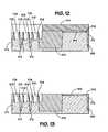
- the technique 100may include performing an STI fill and chemical mechanical polish (“CMP”) on the semiconductor structure, as indicated by block 108 of FIG. 4 and illustrated in the structure of FIG. 9 .
- the STI fillmay include filling the areas etched out by the STI etch with a spin on dielectric (“SOD”) 172 (See FIG. 9 ). In other embodiments, however, other suitable types of dielectric may be used to fill the areas removed by the STI etch 106 .
- the technique 100may also include performing a CMP on the semiconductor structure.
- the CMPmay include a stop on nitride (“SON”) CMP that will polish the SOD fill 172 until the top of the SOD fill 172 is roughly flush with the top of the nitride layer 164 .
- the top of the semiconductor structuremay be polished until the polisher in the CMP device reaches the nitride layer 164 .
- FIG. 9illustrates one embodiment of a semiconductor structure following the STI fill and CMP.
- the technique 100may include etch leveling and a nitride strip, as indicated by block 110 .
- etch levelingmay include a buffer oxide etch using a mixture of ammonia, fluoride, and hydrofluoric acid. In alternate embodiments, however, other suitable types of etch leveling may be employed.
- the nitride strip illustrated in block 110may include a wet nitride strip employing boiling phosphoric acid, but in alternate embodiments, other suitable types of wet nitride strip may be employed in the technique 100 .
- FIG. 10illustrates an exemplary semiconductor structure following the etch leveling and nitride strip (block 110 ).
- the etch leveling and nitride stripremoved the nitride layer 164 and removed the section of the spacers 170 that was roughly adjacent to the nitride layer 164 . It should be noted, however, that the bottom part of the spacers 170 adjacent to the PADOX 162 was not removed by the nitride strip.
- the technique 100may include a damascene process, as indicated by block 112 .
- the damascene processmay include applying a photolithographic mask 174 to cover the parts of the semiconductor structure that will not ultimately be a part of the fin (see FIGS. 11A , 11 B, and 12 ), such as the area of the semiconductor structure that will become contact pads for either the source and/or drain of the semiconductor.
- the damascene processmay also include performing an oxide etch (e.g., an oxide punch) to remove the PADOX 162 (where it is not protected by the mask 174 ), and then performing a silicon etch to create one side of fins 176 . For example, as illustrated by FIGS.
- the spacers 170 and the SOD fill 172each of which is substantially unaffected by the silicon etch, will function as a mask during the silicon etch part of the damascene process.
- the depth of the channels 178i.e., the depth of the silicon etch
- the height of the fins 176may vary between 500 A and 2,000 A with higher fins exhibiting better isolation between memory cells.
- the technique 100may include performing an STI oxide etch to remove the remaining part of the spacer 170 and remove the SOD fill 172 to a depth, as indicated by block 114 .
- the depth of the STI oxide etchwill be roughly approximate to the depth of the channels 178 .
- FIG. 12illustrates an exemplary semiconductor structure after the STI oxide etch removed the spacers 170 and the SOD fill 172 to the same approximate depth as the channels 178 .
- the STI oxide etchcreates one or more double fins 176 (i.e., two fins) extending up from the substrate 160 . As shown in FIG.
- each of the fins 176 in the double finextends upward from an outcropping 182 of substrate that extends upward from the substrate 160 and is partially separated by the SOD 172 from other outcroppings 182 from the substrate 160 .
- each of the fins 176 within a double fin pair, while formed from the substrate 160may extend upward from one of the outcroppings and be partially separated from the other fin 176 in the double fin by the channel 178 .
- a gatemay be formed as indicated by block 118 and depicted in FIGS. 14A and 14B .
- forming the gatemay include depositing silicon and/or polysilicon 180 between and/or around the fins 176 . Because the fins 176 are recessed below the original surface of the substrate 160 , slight misalignments between the gate 180 and the fins 176 will not substantially affect operation of the fin FET. As described above, in one embodiment, the gate 180 is deposited after the fins 176 have been fully formed. Lastly, as also illustrated in FIGS.
- a layer of tungsten silicide 182 or other suitable materialmay be deposited on top of and/or adjacent to the gate 180 to act as a landing pad for context for the fin FET.
- additional contacts 184 for a source and/or drain for the FINFETmay also be formed during block 118 of FIG. 4 .
Landscapes
- Engineering & Computer Science (AREA)
- Physics & Mathematics (AREA)
- Condensed Matter Physics & Semiconductors (AREA)
- General Physics & Mathematics (AREA)
- Manufacturing & Machinery (AREA)
- Computer Hardware Design (AREA)
- Microelectronics & Electronic Packaging (AREA)
- Power Engineering (AREA)
- Insulated Gate Type Field-Effect Transistor (AREA)
- Metal-Oxide And Bipolar Metal-Oxide Semiconductor Integrated Circuits (AREA)
- Thin Film Transistor (AREA)
- Semiconductor Memories (AREA)
Abstract
Description
Claims (15)
Priority Applications (9)
| Application Number | Priority Date | Filing Date | Title |
|---|---|---|---|
| US11/508,047US7745319B2 (en) | 2006-08-22 | 2006-08-22 | System and method for fabricating a fin field effect transistor |
| KR1020097003577AKR101064467B1 (en) | 2006-08-22 | 2007-08-07 | Fin Field Effect Transistor Manufacturing System and Method |
| JP2009525552AJP5299703B2 (en) | 2006-08-22 | 2007-08-07 | Method of manufacturing a transistor including a fin and a gate |
| CN200780030668.9ACN101506957B (en) | 2006-08-22 | 2007-08-07 | Systems and methods for fabricating fin field effect transistors |
| PCT/US2007/017571WO2008024200A1 (en) | 2006-08-22 | 2007-08-07 | System and method for fabricating a fin field effect transistor |
| TW096130937ATWI352394B (en) | 2006-08-22 | 2007-08-21 | System and method for fabricating a fin field effe |
| US12/795,495US8076721B2 (en) | 2006-08-22 | 2010-06-07 | Fin structures and methods of fabricating fin structures |
| US13/324,520US8748280B2 (en) | 2006-08-22 | 2011-12-13 | Methods of fabricating fin structures |
| US14/292,443US9281402B2 (en) | 2006-08-22 | 2014-05-30 | Methods of fabricating fin structures |
Applications Claiming Priority (1)
| Application Number | Priority Date | Filing Date | Title |
|---|---|---|---|
| US11/508,047US7745319B2 (en) | 2006-08-22 | 2006-08-22 | System and method for fabricating a fin field effect transistor |
Related Child Applications (1)
| Application Number | Title | Priority Date | Filing Date |
|---|---|---|---|
| US12/795,495ContinuationUS8076721B2 (en) | 2006-08-22 | 2010-06-07 | Fin structures and methods of fabricating fin structures |
Publications (2)
| Publication Number | Publication Date |
|---|---|
| US20080050885A1 US20080050885A1 (en) | 2008-02-28 |
| US7745319B2true US7745319B2 (en) | 2010-06-29 |
Family
ID=38652384
Family Applications (4)
| Application Number | Title | Priority Date | Filing Date |
|---|---|---|---|
| US11/508,047Active2027-07-20US7745319B2 (en) | 2006-08-22 | 2006-08-22 | System and method for fabricating a fin field effect transistor |
| US12/795,495ActiveUS8076721B2 (en) | 2006-08-22 | 2010-06-07 | Fin structures and methods of fabricating fin structures |
| US13/324,520Active2027-02-03US8748280B2 (en) | 2006-08-22 | 2011-12-13 | Methods of fabricating fin structures |
| US14/292,443Active2026-09-02US9281402B2 (en) | 2006-08-22 | 2014-05-30 | Methods of fabricating fin structures |
Family Applications After (3)
| Application Number | Title | Priority Date | Filing Date |
|---|---|---|---|
| US12/795,495ActiveUS8076721B2 (en) | 2006-08-22 | 2010-06-07 | Fin structures and methods of fabricating fin structures |
| US13/324,520Active2027-02-03US8748280B2 (en) | 2006-08-22 | 2011-12-13 | Methods of fabricating fin structures |
| US14/292,443Active2026-09-02US9281402B2 (en) | 2006-08-22 | 2014-05-30 | Methods of fabricating fin structures |
Country Status (6)
| Country | Link |
|---|---|
| US (4) | US7745319B2 (en) |
| JP (1) | JP5299703B2 (en) |
| KR (1) | KR101064467B1 (en) |
| CN (1) | CN101506957B (en) |
| TW (1) | TWI352394B (en) |
| WO (1) | WO2008024200A1 (en) |
Cited By (9)
| Publication number | Priority date | Publication date | Assignee | Title |
|---|---|---|---|---|
| US20090305492A1 (en)* | 2006-09-06 | 2009-12-10 | International Business Machines Corporation | Vertical field effect transistor arrays and methods for fabrication thereof |
| US20110097863A1 (en)* | 2009-10-27 | 2011-04-28 | Taiwan Semiconductor Manufacturing Company, Ltd. | Cross OD FinFET Patterning |
| US8987111B2 (en) | 2012-03-30 | 2015-03-24 | Samsung Electronics Co., Ltd. | Method of manufacturing a three dimensional array having buried word lines of different heights and widths |
| US8987836B2 (en) | 2012-04-23 | 2015-03-24 | Samsung Electronics Co., Ltd. | Field effect transistor having fin base and at lease one fin protruding from fin base |
| US9006067B2 (en) | 2013-02-14 | 2015-04-14 | Samsung Electronics Co., Ltd. | Semiconductor device and method of fabricationg the same |
| US9130058B2 (en) | 2010-07-26 | 2015-09-08 | Taiwan Semiconductor Manufacturing Company, Ltd. | Forming crown active regions for FinFETs |
| US9601628B2 (en) | 2015-01-15 | 2017-03-21 | Samsung Electronics Co., Ltd. | Semiconductor device having asymmetric fin-shaped pattern |
| US9929155B2 (en) | 2015-04-02 | 2018-03-27 | Samsung Electronics Co., Ltd. | Semiconductor device having symmetric and asymmetric active fins |
| US11088142B2 (en) | 2019-12-26 | 2021-08-10 | Micron Technology, Inc. | Integrated assemblies having voids along regions of gates, and methods of forming conductive structures |
Families Citing this family (22)
| Publication number | Priority date | Publication date | Assignee | Title |
|---|---|---|---|---|
| US6949795B2 (en)* | 2003-11-13 | 2005-09-27 | Micron Technology, Inc. | Structure and method of fabricating a transistor having a trench gate |
| US7745319B2 (en)* | 2006-08-22 | 2010-06-29 | Micron Technology, Inc. | System and method for fabricating a fin field effect transistor |
| US7808042B2 (en) | 2008-03-20 | 2010-10-05 | Micron Technology, Inc. | Systems and devices including multi-gate transistors and methods of using, making, and operating the same |
| JP5301912B2 (en)* | 2008-07-31 | 2013-09-25 | ルネサスエレクトロニクス株式会社 | Manufacturing method of semiconductor device |
| US9368388B2 (en)* | 2012-04-13 | 2016-06-14 | Taiwan Semiconductor Manufacturing Company, Ltd. | Apparatus for FinFETs |
| US9633905B2 (en) | 2012-04-20 | 2017-04-25 | Taiwan Semiconductor Manufacturing Company, Ltd. | Semiconductor fin structures and methods for forming the same |
| US11037923B2 (en) | 2012-06-29 | 2021-06-15 | Intel Corporation | Through gate fin isolation |
| US9142400B1 (en) | 2012-07-17 | 2015-09-22 | Stc.Unm | Method of making a heteroepitaxial layer on a seed area |
| US8841185B2 (en) | 2012-08-13 | 2014-09-23 | International Business Machines Corporation | High density bulk fin capacitor |
| US8658536B1 (en)* | 2012-09-05 | 2014-02-25 | Globalfoundries Inc. | Selective fin cut process |
| US8946050B2 (en) | 2012-10-30 | 2015-02-03 | Globalfoundries Inc. | Double trench well formation in SRAM cells |
| US9412847B2 (en) | 2013-03-11 | 2016-08-09 | Taiwan Semiconductor Manufacturing Company, Ltd. | Self-aligned passivation of active regions |
| EP3072147A4 (en)* | 2013-11-20 | 2017-09-13 | Intel Corporation | Microelectronic transistor contacts and methods of fabricating the same |
| US10504893B2 (en) | 2014-08-29 | 2019-12-10 | Taiwan Semiconductor Manufacturing Co., Ltd. | Fin field effect transistor (FinFET) device with protection layer |
| US9818647B2 (en) | 2015-06-03 | 2017-11-14 | International Business Machines Corporation | Germanium dual-fin field effect transistor |
| CN106711213B (en)* | 2015-07-20 | 2021-02-26 | 联华电子股份有限公司 | Semiconductor element and manufacturing method thereof |
| US11017999B2 (en) | 2016-10-05 | 2021-05-25 | International Business Machines Corporation | Method and structure for forming bulk FinFET with uniform channel height |
| CN110034068B (en)* | 2018-01-11 | 2021-07-13 | 中芯国际集成电路制造(上海)有限公司 | Semiconductor structure and method of forming the same |
| KR102620595B1 (en) | 2018-01-22 | 2024-01-03 | 삼성전자주식회사 | Semiconductor device including insulating layers and method of manufacturing the same |
| CN113488430B (en)* | 2018-04-03 | 2023-04-25 | 长鑫存储技术有限公司 | Forming method of self-aligned groove |
| US10381218B1 (en) | 2018-05-17 | 2019-08-13 | Micron Technology, Inc. | Methods of forming a semiconductor structure and methods of forming isolation structures |
| DE102020112203B4 (en) | 2020-03-13 | 2024-08-08 | Taiwan Semiconductor Manufacturing Co. Ltd. | INTEGRATED CIRCUIT AND METHOD FOR EMBEDDED PLANAR FETS WITH FINFETS |
Citations (27)
| Publication number | Priority date | Publication date | Assignee | Title |
|---|---|---|---|---|
| US5021353A (en) | 1990-02-26 | 1991-06-04 | Micron Technology, Inc. | Split-polysilicon CMOS process incorporating self-aligned silicidation of conductive regions |
| US5177027A (en) | 1990-08-17 | 1993-01-05 | Micron Technology, Inc. | Process for fabricating, on the edge of a silicon mesa, a MOSFET which has a spacer-shaped gate and a right-angled channel path |
| US5804506A (en) | 1995-08-17 | 1998-09-08 | Micron Technology, Inc. | Acceleration of etch selectivity for self-aligned contact |
| US6060783A (en) | 1995-12-07 | 2000-05-09 | Micron Technology, Inc | Self-aligned contact plugs |
| US6110798A (en)* | 1996-01-05 | 2000-08-29 | Micron Technology, Inc. | Method of fabricating an isolation structure on a semiconductor substrate |
| US6346455B1 (en) | 2000-08-31 | 2002-02-12 | Micron Technology, Inc. | Method to form a corrugated structure for enhanced capacitance |
| US6376380B1 (en) | 2000-08-30 | 2002-04-23 | Micron Technology, Inc. | Method of forming memory circuitry and method of forming memory circuitry comprising a buried bit line array of memory cells |
| US20020179970A1 (en)* | 1999-06-30 | 2002-12-05 | Kabushiki Kaisha Toshiba | Semiconductor device and method of manufacturing the same |
| US6492212B1 (en) | 2001-10-05 | 2002-12-10 | International Business Machines Corporation | Variable threshold voltage double gated transistors and method of fabrication |
| US20040191980A1 (en)* | 2003-03-27 | 2004-09-30 | Rafael Rios | Multi-corner FET for better immunity from short channel effects |
| US20040251487A1 (en) | 2003-06-12 | 2004-12-16 | Yider Wu | Non-volatile memory device |
| US20050035391A1 (en)* | 2003-08-14 | 2005-02-17 | Lee Deok Hyung | Multi-structured Si-fin and method of manufacture |
| US20050110085A1 (en) | 2003-11-20 | 2005-05-26 | Huilong Zhu | Dual gate finfet |
| US6903425B2 (en) | 2002-08-05 | 2005-06-07 | Micron Technology, Inc. | Silicon rich barrier layers for integrated circuit devices |
| US20050179030A1 (en) | 2004-02-13 | 2005-08-18 | Hyeoung-Won Seo | Field effect transistor device with channel fin structure and method of fabricating the same |
| US6936507B2 (en) | 2002-08-15 | 2005-08-30 | Micron Technology, Inc. | Method of forming field effect transistors |
| US20050205945A1 (en)* | 2004-03-18 | 2005-09-22 | Jung-Sok Lee | Field effect transistor and method of manufacturing same |
| US20050266638A1 (en) | 2004-05-31 | 2005-12-01 | Cho Eun-Suk | Methods of forming non-volatile memory cells including fin structures and related devices |
| US20050275040A1 (en) | 2004-06-11 | 2005-12-15 | International Business Machines Corporation | Back gate finfet sram |
| US20060043471A1 (en) | 2004-08-26 | 2006-03-02 | Tang Sanh D | Vertical transistor structures having vertical-surrounding-gates with self-aligned features |
| US20060046424A1 (en) | 2004-08-24 | 2006-03-02 | Chance Randal W | Methods of forming semiconductor constructions |
| US20060043450A1 (en) | 2004-09-02 | 2006-03-02 | Tang Sanh D | Vertical transistors |
| US20060043449A1 (en) | 2004-09-01 | 2006-03-02 | Tang Sanh D | Semiconductor constructions and transistors, and methods of forming semiconductor constructions and transistors |
| US20060046391A1 (en) | 2004-08-30 | 2006-03-02 | Tang Sanh D | Vertical wrap-around-gate field-effect-transistor for high density, low voltage logic and memory array |
| US20060125044A1 (en) | 2004-12-13 | 2006-06-15 | Haller Gordon A | Methods of reducing floating body effect |
| US20060151880A1 (en) | 2005-01-10 | 2006-07-13 | Micron Technology, Inc. | Interconnect structures with bond-pads and methods of forming bump sites on bond-pads |
| US7265059B2 (en)* | 2005-09-30 | 2007-09-04 | Freescale Semiconductor, Inc. | Multiple fin formation |
Family Cites Families (10)
| Publication number | Priority date | Publication date | Assignee | Title |
|---|---|---|---|---|
| US6018180A (en)* | 1997-12-23 | 2000-01-25 | Advanced Micro Devices, Inc. | Transistor formation with LI overetch immunity |
| JP2003031116A (en)* | 2001-07-17 | 2003-01-31 | Nec Corp | Field emission cold cathode and its manufacturing method and plane image device having field emission cathode |
| KR100594282B1 (en)* | 2004-06-28 | 2006-06-30 | 삼성전자주식회사 | Semiconductor device comprising FIFNFETT and method for manufacturing same |
| US7442976B2 (en)* | 2004-09-01 | 2008-10-28 | Micron Technology, Inc. | DRAM cells with vertical transistors |
| JP2006128494A (en)* | 2004-10-29 | 2006-05-18 | Toshiba Corp | Semiconductor integrated circuit device and manufacturing method thereof |
| JP2006135067A (en)* | 2004-11-05 | 2006-05-25 | Toshiba Corp | Semiconductor device and manufacturing method thereof |
| JP2006196617A (en)* | 2005-01-12 | 2006-07-27 | Fujitsu Ltd | Semiconductor device manufacturing method and semiconductor device manufactured by the method |
| JP4672400B2 (en)* | 2005-03-09 | 2011-04-20 | 株式会社東芝 | Perhydrogenated polysilazane solution and method for manufacturing semiconductor device using the same |
| US7745319B2 (en)* | 2006-08-22 | 2010-06-29 | Micron Technology, Inc. | System and method for fabricating a fin field effect transistor |
| US8866254B2 (en)* | 2008-02-19 | 2014-10-21 | Micron Technology, Inc. | Devices including fin transistors robust to gate shorts and methods of making the same |
- 2006
- 2006-08-22USUS11/508,047patent/US7745319B2/enactiveActive
- 2007
- 2007-08-07KRKR1020097003577Apatent/KR101064467B1/enactiveActive
- 2007-08-07CNCN200780030668.9Apatent/CN101506957B/enactiveActive
- 2007-08-07WOPCT/US2007/017571patent/WO2008024200A1/enactiveApplication Filing
- 2007-08-07JPJP2009525552Apatent/JP5299703B2/enactiveActive
- 2007-08-21TWTW096130937Apatent/TWI352394B/enactive
- 2010
- 2010-06-07USUS12/795,495patent/US8076721B2/enactiveActive
- 2011
- 2011-12-13USUS13/324,520patent/US8748280B2/enactiveActive
- 2014
- 2014-05-30USUS14/292,443patent/US9281402B2/enactiveActive
Patent Citations (31)
| Publication number | Priority date | Publication date | Assignee | Title |
|---|---|---|---|---|
| US5021353A (en) | 1990-02-26 | 1991-06-04 | Micron Technology, Inc. | Split-polysilicon CMOS process incorporating self-aligned silicidation of conductive regions |
| US5177027A (en) | 1990-08-17 | 1993-01-05 | Micron Technology, Inc. | Process for fabricating, on the edge of a silicon mesa, a MOSFET which has a spacer-shaped gate and a right-angled channel path |
| US5804506A (en) | 1995-08-17 | 1998-09-08 | Micron Technology, Inc. | Acceleration of etch selectivity for self-aligned contact |
| US6060783A (en) | 1995-12-07 | 2000-05-09 | Micron Technology, Inc | Self-aligned contact plugs |
| US6469389B2 (en) | 1995-12-07 | 2002-10-22 | Micron Technolgy, Inc. | Contact plug |
| US6110798A (en)* | 1996-01-05 | 2000-08-29 | Micron Technology, Inc. | Method of fabricating an isolation structure on a semiconductor substrate |
| US20020179970A1 (en)* | 1999-06-30 | 2002-12-05 | Kabushiki Kaisha Toshiba | Semiconductor device and method of manufacturing the same |
| US6376380B1 (en) | 2000-08-30 | 2002-04-23 | Micron Technology, Inc. | Method of forming memory circuitry and method of forming memory circuitry comprising a buried bit line array of memory cells |
| US6346455B1 (en) | 2000-08-31 | 2002-02-12 | Micron Technology, Inc. | Method to form a corrugated structure for enhanced capacitance |
| US6492212B1 (en) | 2001-10-05 | 2002-12-10 | International Business Machines Corporation | Variable threshold voltage double gated transistors and method of fabrication |
| US6903425B2 (en) | 2002-08-05 | 2005-06-07 | Micron Technology, Inc. | Silicon rich barrier layers for integrated circuit devices |
| US7071049B2 (en) | 2002-08-05 | 2006-07-04 | Micron Technology, Inc. | Silicon rich barrier layers for integrated circuit devices |
| US7071043B2 (en) | 2002-08-15 | 2006-07-04 | Micron Technology, Inc. | Methods of forming a field effect transistor having source/drain material over insulative material |
| US6936507B2 (en) | 2002-08-15 | 2005-08-30 | Micron Technology, Inc. | Method of forming field effect transistors |
| US20040191980A1 (en)* | 2003-03-27 | 2004-09-30 | Rafael Rios | Multi-corner FET for better immunity from short channel effects |
| US20040251487A1 (en) | 2003-06-12 | 2004-12-16 | Yider Wu | Non-volatile memory device |
| US20050035391A1 (en)* | 2003-08-14 | 2005-02-17 | Lee Deok Hyung | Multi-structured Si-fin and method of manufacture |
| US20050110085A1 (en) | 2003-11-20 | 2005-05-26 | Huilong Zhu | Dual gate finfet |
| US20050179030A1 (en) | 2004-02-13 | 2005-08-18 | Hyeoung-Won Seo | Field effect transistor device with channel fin structure and method of fabricating the same |
| US20050205945A1 (en)* | 2004-03-18 | 2005-09-22 | Jung-Sok Lee | Field effect transistor and method of manufacturing same |
| US20050266638A1 (en) | 2004-05-31 | 2005-12-01 | Cho Eun-Suk | Methods of forming non-volatile memory cells including fin structures and related devices |
| US20050275040A1 (en) | 2004-06-11 | 2005-12-15 | International Business Machines Corporation | Back gate finfet sram |
| US20060046424A1 (en) | 2004-08-24 | 2006-03-02 | Chance Randal W | Methods of forming semiconductor constructions |
| US20060063350A1 (en) | 2004-08-24 | 2006-03-23 | Chance Randal W | Semiconductor constructions |
| US20060043471A1 (en) | 2004-08-26 | 2006-03-02 | Tang Sanh D | Vertical transistor structures having vertical-surrounding-gates with self-aligned features |
| US20060046391A1 (en) | 2004-08-30 | 2006-03-02 | Tang Sanh D | Vertical wrap-around-gate field-effect-transistor for high density, low voltage logic and memory array |
| US20060043449A1 (en) | 2004-09-01 | 2006-03-02 | Tang Sanh D | Semiconductor constructions and transistors, and methods of forming semiconductor constructions and transistors |
| US20060043450A1 (en) | 2004-09-02 | 2006-03-02 | Tang Sanh D | Vertical transistors |
| US20060125044A1 (en) | 2004-12-13 | 2006-06-15 | Haller Gordon A | Methods of reducing floating body effect |
| US20060151880A1 (en) | 2005-01-10 | 2006-07-13 | Micron Technology, Inc. | Interconnect structures with bond-pads and methods of forming bump sites on bond-pads |
| US7265059B2 (en)* | 2005-09-30 | 2007-09-04 | Freescale Semiconductor, Inc. | Multiple fin formation |
Non-Patent Citations (6)
| Title |
|---|
| F. Fishburn, B. Busch, J. Dale, D. Hwang, R. Lane, T. McDaniel, S. Southwick, R. Turi, H. Wang, and L. Tran, A 78nm 6F2 DRAM Technology for Multigigabit Densities, Micron Technology, Inc. - Process R&D Center, Boise, Idaho. |
| F. Fishburn, B. Busch, J. Dale, D. Hwang, R. Lane, T. McDaniel, S. Southwick, R. Turi, H. Wang, and L. Tran, A 78nm 6F2 DRAM Technology for Multigigabit Densities, Micron Technology, Inc. — Process R&D Center, Boise, Idaho. |
| J.C. Sturm and K. Tokunaga, Increased Transconductance in Fully-Depleted Ultra-Thin Silicon-on-Insulator Mosfet's, Department of Electrical Engineering, Princeton University, Princeton, NJ. |
| Leland Chang, Yang-Kyu Choi, Daewon Ha, Pushkar Ranade, Shiying Xiong, Jeffrey Bokor, Chenming Hu, and Tus-Jae King, Extremely Scaled Silicon Nano-CMOS Devices, IEEE, vol. 91, No. 11, Nov. 2003, pp. 1860-1873. |
| R. Katsumata, N. Tsuda, J. Idebuchi, M. Kondo, N. Aoki, S. Ito, K. Yahashi, T. Satonaka, M. Morikado, M. Kito, M. Kido, T. Tanaka, H. Aochi and T. Hamaoto, Fin-Array-FET on Bulk Silicon for Sub-100 nm Trench Capacitor DRAM, 2003 Symposium on VLSI Technology Digest of Technical Papers. |
| T. Park, S. Choi, D.H. Lee, J.R. Yoo, B.C. Lee, J.Y. Kim, C.G. Lee, K.K. Chi, S.H. Hong, S.J. Syun, Y.G. Shin, J.N. Han, I.S. Park, U.I. Chung, J.T. Moon, E. Yoon, and J.H. Lee, Fabrication of Body-Tied Fin FETs (Omega MOSFETs) Using Bulk Si Wafters, 2003 Symposium on VLSI Technology Digest of Technical Papers. |
Cited By (24)
| Publication number | Priority date | Publication date | Assignee | Title |
|---|---|---|---|---|
| US20090305492A1 (en)* | 2006-09-06 | 2009-12-10 | International Business Machines Corporation | Vertical field effect transistor arrays and methods for fabrication thereof |
| US20100301409A1 (en)* | 2006-09-06 | 2010-12-02 | International Business Machines Corporation | Vertical field effect transistor arrays and methods for fabrication thereof |
| US7981748B2 (en)* | 2006-09-06 | 2011-07-19 | International Business Machines Corporation | Method for fabricating a vertical field effect transistor array comprising a plurality of semiconductor pillars |
| US8110901B2 (en) | 2006-09-06 | 2012-02-07 | International Business Machines Corporation | Vertical field effect transistor arrays including gate electrodes annularly surrounding semiconductor pillars |
| US8383501B2 (en) | 2006-09-06 | 2013-02-26 | International Business Machines Corporation | Vertical field effect transistor arrays and methods for fabrication thereof |
| US20110097863A1 (en)* | 2009-10-27 | 2011-04-28 | Taiwan Semiconductor Manufacturing Company, Ltd. | Cross OD FinFET Patterning |
| US8110466B2 (en)* | 2009-10-27 | 2012-02-07 | Taiwan Semiconductor Manufacturing Company, Ltd. | Cross OD FinFET patterning |
| US20120100673A1 (en)* | 2009-10-27 | 2012-04-26 | Taiwan Semiconductor Manufacturing Company, Ltd. | Cross OD FinFET Patterning |
| US8796156B2 (en)* | 2009-10-27 | 2014-08-05 | Taiwan Semiconductor Manufacturing Company, Ltd. | Cross OD FinFET patterning |
| US9130058B2 (en) | 2010-07-26 | 2015-09-08 | Taiwan Semiconductor Manufacturing Company, Ltd. | Forming crown active regions for FinFETs |
| US9543210B2 (en) | 2010-07-26 | 2017-01-10 | Taiwan Semiconductor Manufacturing Company, Ltd. | Forming crown active regions for FinFETs |
| US8987111B2 (en) | 2012-03-30 | 2015-03-24 | Samsung Electronics Co., Ltd. | Method of manufacturing a three dimensional array having buried word lines of different heights and widths |
| US8987836B2 (en) | 2012-04-23 | 2015-03-24 | Samsung Electronics Co., Ltd. | Field effect transistor having fin base and at lease one fin protruding from fin base |
| USRE49375E1 (en) | 2012-04-23 | 2023-01-17 | Samsung Electronics Co., Ltd. | Field effect transistor having fin base and at least one fin protruding from fin base |
| USRE48367E1 (en) | 2012-04-23 | 2020-12-22 | Samsung Electronics Co., Ltd. | Field effect transistor having fin base and at least one fin protruding from fin base |
| US9006067B2 (en) | 2013-02-14 | 2015-04-14 | Samsung Electronics Co., Ltd. | Semiconductor device and method of fabricationg the same |
| US10199377B2 (en) | 2015-01-15 | 2019-02-05 | Samsung Electronics Co., Ltd. | Semiconductor device having asymmetric fin-shaped pattern |
| US10692864B2 (en) | 2015-01-15 | 2020-06-23 | Samsung Electronics Co., Ltd. | Semiconductor device having asymmetric fin-shaped pattern |
| US10910373B2 (en) | 2015-01-15 | 2021-02-02 | Samsung Electronics Co., Ltd. | Semiconductor device having asymmetric fin-shaped pattern |
| US9601628B2 (en) | 2015-01-15 | 2017-03-21 | Samsung Electronics Co., Ltd. | Semiconductor device having asymmetric fin-shaped pattern |
| US9929155B2 (en) | 2015-04-02 | 2018-03-27 | Samsung Electronics Co., Ltd. | Semiconductor device having symmetric and asymmetric active fins |
| US11088142B2 (en) | 2019-12-26 | 2021-08-10 | Micron Technology, Inc. | Integrated assemblies having voids along regions of gates, and methods of forming conductive structures |
| US11456299B2 (en) | 2019-12-26 | 2022-09-27 | Micron Technology, Inc. | Integrated assemblies having voids along regions of gates, and methods of forming conductive structures |
| US12150292B2 (en) | 2019-12-26 | 2024-11-19 | Micron Technology, Inc. | Integrated assemblies having voids along regions of gates, and methods of forming conductive structures |
Also Published As
| Publication number | Publication date |
|---|---|
| US20080050885A1 (en) | 2008-02-28 |
| CN101506957A (en) | 2009-08-12 |
| JP2010502009A (en) | 2010-01-21 |
| US20140346613A1 (en) | 2014-11-27 |
| US20100252886A1 (en) | 2010-10-07 |
| US8076721B2 (en) | 2011-12-13 |
| TWI352394B (en) | 2011-11-11 |
| TW200818338A (en) | 2008-04-16 |
| US8748280B2 (en) | 2014-06-10 |
| US20120088349A1 (en) | 2012-04-12 |
| WO2008024200A1 (en) | 2008-02-28 |
| KR101064467B1 (en) | 2011-09-15 |
| US9281402B2 (en) | 2016-03-08 |
| CN101506957B (en) | 2015-11-25 |
| JP5299703B2 (en) | 2013-09-25 |
| KR20090042275A (en) | 2009-04-29 |
Similar Documents
| Publication | Publication Date | Title |
|---|---|---|
| US7745319B2 (en) | System and method for fabricating a fin field effect transistor | |
| US7993988B2 (en) | Techniques for fabricating a non-planar transistor | |
| US9741854B2 (en) | Method for manufacturing semiconductor device | |
| US9385132B2 (en) | Arrays of recessed access devices, methods of forming recessed access gate constructions, and methods of forming isolation gate constructions in the fabrication of recessed access devices | |
| US12274049B2 (en) | Memory devices having vertical transistors and stacked storage units and methods for forming the same | |
| US12082399B2 (en) | Memory devices having vertical transistors in staggered layouts | |
| US20140327056A1 (en) | Semiconductor device having contact plug and method of manufacturing the same | |
| KR20130015428A (en) | Semiconductor device | |
| US12328867B2 (en) | Memory devices having vertical transistors and methods for forming the same | |
| US20230134556A1 (en) | Memory devices having vertical transistors and methods for forming the same | |
| CN101188239A (en) | Semiconductor device and method of forming the same | |
| CN102122656A (en) | Vertical type integrated circuit devices and memory devices | |
| US7736989B2 (en) | Method of forming semiconductor device | |
| KR101785447B1 (en) | Method of manufacturing semiconductor device | |
| US9142536B2 (en) | Semiconductor device and method for fabricating the same | |
| KR102684455B1 (en) | U-shaped channel access transistors and methods for forming the same | |
| US9754944B2 (en) | Method of manufacturing semiconductor device | |
| US12127393B2 (en) | Memory devices having vertical transistors and methods for forming the same |
Legal Events
| Date | Code | Title | Description |
|---|---|---|---|
| AS | Assignment | Owner name:MICRON TECHNOLOGY INC., IDAHO Free format text:ASSIGNMENT OF ASSIGNORS INTEREST;ASSIGNORS:TANG, SANH D.;HALLER, GORDON;REEL/FRAME:018212/0189 Effective date:20060822 Owner name:MICRON TECHNOLOGY INC.,IDAHO Free format text:ASSIGNMENT OF ASSIGNORS INTEREST;ASSIGNORS:TANG, SANH D.;HALLER, GORDON;REEL/FRAME:018212/0189 Effective date:20060822 | |
| FEPP | Fee payment procedure | Free format text:PAYER NUMBER DE-ASSIGNED (ORIGINAL EVENT CODE: RMPN); ENTITY STATUS OF PATENT OWNER: LARGE ENTITY Free format text:PAYOR NUMBER ASSIGNED (ORIGINAL EVENT CODE: ASPN); ENTITY STATUS OF PATENT OWNER: LARGE ENTITY | |
| STCF | Information on status: patent grant | Free format text:PATENTED CASE | |
| FPAY | Fee payment | Year of fee payment:4 | |
| AS | Assignment | Owner name:U.S. BANK NATIONAL ASSOCIATION, AS COLLATERAL AGENT, CALIFORNIA Free format text:SECURITY INTEREST;ASSIGNOR:MICRON TECHNOLOGY, INC.;REEL/FRAME:038669/0001 Effective date:20160426 Owner name:U.S. BANK NATIONAL ASSOCIATION, AS COLLATERAL AGEN Free format text:SECURITY INTEREST;ASSIGNOR:MICRON TECHNOLOGY, INC.;REEL/FRAME:038669/0001 Effective date:20160426 | |
| AS | Assignment | Owner name:MORGAN STANLEY SENIOR FUNDING, INC., AS COLLATERAL AGENT, MARYLAND Free format text:PATENT SECURITY AGREEMENT;ASSIGNOR:MICRON TECHNOLOGY, INC.;REEL/FRAME:038954/0001 Effective date:20160426 Owner name:MORGAN STANLEY SENIOR FUNDING, INC., AS COLLATERAL Free format text:PATENT SECURITY AGREEMENT;ASSIGNOR:MICRON TECHNOLOGY, INC.;REEL/FRAME:038954/0001 Effective date:20160426 | |
| AS | Assignment | Owner name:U.S. BANK NATIONAL ASSOCIATION, AS COLLATERAL AGENT, CALIFORNIA Free format text:CORRECTIVE ASSIGNMENT TO CORRECT THE REPLACE ERRONEOUSLY FILED PATENT #7358718 WITH THE CORRECT PATENT #7358178 PREVIOUSLY RECORDED ON REEL 038669 FRAME 0001. ASSIGNOR(S) HEREBY CONFIRMS THE SECURITY INTEREST;ASSIGNOR:MICRON TECHNOLOGY, INC.;REEL/FRAME:043079/0001 Effective date:20160426 Owner name:U.S. BANK NATIONAL ASSOCIATION, AS COLLATERAL AGEN Free format text:CORRECTIVE ASSIGNMENT TO CORRECT THE REPLACE ERRONEOUSLY FILED PATENT #7358718 WITH THE CORRECT PATENT #7358178 PREVIOUSLY RECORDED ON REEL 038669 FRAME 0001. ASSIGNOR(S) HEREBY CONFIRMS THE SECURITY INTEREST;ASSIGNOR:MICRON TECHNOLOGY, INC.;REEL/FRAME:043079/0001 Effective date:20160426 | |
| MAFP | Maintenance fee payment | Free format text:PAYMENT OF MAINTENANCE FEE, 8TH YEAR, LARGE ENTITY (ORIGINAL EVENT CODE: M1552) Year of fee payment:8 | |
| AS | Assignment | Owner name:JPMORGAN CHASE BANK, N.A., AS COLLATERAL AGENT, ILLINOIS Free format text:SECURITY INTEREST;ASSIGNORS:MICRON TECHNOLOGY, INC.;MICRON SEMICONDUCTOR PRODUCTS, INC.;REEL/FRAME:047540/0001 Effective date:20180703 Owner name:JPMORGAN CHASE BANK, N.A., AS COLLATERAL AGENT, IL Free format text:SECURITY INTEREST;ASSIGNORS:MICRON TECHNOLOGY, INC.;MICRON SEMICONDUCTOR PRODUCTS, INC.;REEL/FRAME:047540/0001 Effective date:20180703 | |
| AS | Assignment | Owner name:MICRON TECHNOLOGY, INC., IDAHO Free format text:RELEASE BY SECURED PARTY;ASSIGNOR:U.S. BANK NATIONAL ASSOCIATION, AS COLLATERAL AGENT;REEL/FRAME:047243/0001 Effective date:20180629 | |
| AS | Assignment | Owner name:MICRON TECHNOLOGY, INC., IDAHO Free format text:RELEASE BY SECURED PARTY;ASSIGNOR:MORGAN STANLEY SENIOR FUNDING, INC., AS COLLATERAL AGENT;REEL/FRAME:050937/0001 Effective date:20190731 | |
| AS | Assignment | Owner name:MICRON SEMICONDUCTOR PRODUCTS, INC., IDAHO Free format text:RELEASE BY SECURED PARTY;ASSIGNOR:JPMORGAN CHASE BANK, N.A., AS COLLATERAL AGENT;REEL/FRAME:051028/0001 Effective date:20190731 Owner name:MICRON TECHNOLOGY, INC., IDAHO Free format text:RELEASE BY SECURED PARTY;ASSIGNOR:JPMORGAN CHASE BANK, N.A., AS COLLATERAL AGENT;REEL/FRAME:051028/0001 Effective date:20190731 | |
| MAFP | Maintenance fee payment | Free format text:PAYMENT OF MAINTENANCE FEE, 12TH YEAR, LARGE ENTITY (ORIGINAL EVENT CODE: M1553); ENTITY STATUS OF PATENT OWNER: LARGE ENTITY Year of fee payment:12 |