US7745277B2 - MOSFET performance improvement using deformation in SOI structure - Google Patents
MOSFET performance improvement using deformation in SOI structureDownload PDFInfo
- Publication number
- US7745277B2 US7745277B2US11/065,061US6506105AUS7745277B2US 7745277 B2US7745277 B2US 7745277B2US 6506105 AUS6506105 AUS 6506105AUS 7745277 B2US7745277 B2US 7745277B2
- Authority
- US
- United States
- Prior art keywords
- region
- semiconductor layer
- substrate
- oxide layer
- ion
- Prior art date
- Legal status (The legal status is an assumption and is not a legal conclusion. Google has not performed a legal analysis and makes no representation as to the accuracy of the status listed.)
- Expired - Fee Related
Links
- 239000004065semiconductorSubstances0.000claimsabstractdescription75
- 239000000758substrateSubstances0.000claimsabstractdescription59
- 238000000034methodMethods0.000claimsabstractdescription33
- 238000004519manufacturing processMethods0.000claimsabstractdescription10
- 230000006835compressionEffects0.000claimsdescription25
- 238000007906compressionMethods0.000claimsdescription25
- 238000002513implantationMethods0.000claimsdescription12
- 238000000137annealingMethods0.000claimsdescription11
- 238000002955isolationMethods0.000claimsdescription9
- XUIMIQQOPSSXEZ-UHFFFAOYSA-NSiliconChemical compound[Si]XUIMIQQOPSSXEZ-UHFFFAOYSA-N0.000claimsdescription8
- 229910052710siliconInorganic materials0.000claimsdescription8
- 239000010703siliconSubstances0.000claimsdescription8
- 230000000873masking effectEffects0.000claimsdescription7
- 229910052756noble gasInorganic materials0.000claimsdescription3
- 239000000463materialSubstances0.000description3
- VYPSYNLAJGMNEJ-UHFFFAOYSA-NSilicium dioxideChemical compoundO=[Si]=OVYPSYNLAJGMNEJ-UHFFFAOYSA-N0.000description2
- 238000005468ion implantationMethods0.000description2
- 238000009413insulationMethods0.000description1
- 230000004048modificationEffects0.000description1
- 238000012986modificationMethods0.000description1
- 230000003647oxidationEffects0.000description1
- 238000007254oxidation reactionMethods0.000description1
- 238000000206photolithographyMethods0.000description1
- 235000012239silicon dioxideNutrition0.000description1
- 239000000377silicon dioxideSubstances0.000description1
Images


Classifications
- H—ELECTRICITY
- H10—SEMICONDUCTOR DEVICES; ELECTRIC SOLID-STATE DEVICES NOT OTHERWISE PROVIDED FOR
- H10D—INORGANIC ELECTRIC SEMICONDUCTOR DEVICES
- H10D86/00—Integrated devices formed in or on insulating or conducting substrates, e.g. formed in silicon-on-insulator [SOI] substrates or on stainless steel or glass substrates
- H10D86/01—Manufacture or treatment
- H—ELECTRICITY
- H01—ELECTRIC ELEMENTS
- H01L—SEMICONDUCTOR DEVICES NOT COVERED BY CLASS H10
- H01L21/00—Processes or apparatus adapted for the manufacture or treatment of semiconductor or solid state devices or of parts thereof
- H01L21/70—Manufacture or treatment of devices consisting of a plurality of solid state components formed in or on a common substrate or of parts thereof; Manufacture of integrated circuit devices or of parts thereof
- H01L21/71—Manufacture of specific parts of devices defined in group H01L21/70
- H01L21/76—Making of isolation regions between components
- H01L21/762—Dielectric regions, e.g. EPIC dielectric isolation, LOCOS; Trench refilling techniques, SOI technology, use of channel stoppers
- H01L21/7624—Dielectric regions, e.g. EPIC dielectric isolation, LOCOS; Trench refilling techniques, SOI technology, use of channel stoppers using semiconductor on insulator [SOI] technology
- H—ELECTRICITY
- H10—SEMICONDUCTOR DEVICES; ELECTRIC SOLID-STATE DEVICES NOT OTHERWISE PROVIDED FOR
- H10D—INORGANIC ELECTRIC SEMICONDUCTOR DEVICES
- H10D30/00—Field-effect transistors [FET]
- H10D30/60—Insulated-gate field-effect transistors [IGFET]
- H10D30/791—Arrangements for exerting mechanical stress on the crystal lattice of the channel regions
- H10D30/798—Arrangements for exerting mechanical stress on the crystal lattice of the channel regions being provided in or under the channel regions
- H—ELECTRICITY
- H10—SEMICONDUCTOR DEVICES; ELECTRIC SOLID-STATE DEVICES NOT OTHERWISE PROVIDED FOR
- H10D—INORGANIC ELECTRIC SEMICONDUCTOR DEVICES
- H10D86/00—Integrated devices formed in or on insulating or conducting substrates, e.g. formed in silicon-on-insulator [SOI] substrates or on stainless steel or glass substrates
- H10D86/201—Integrated devices formed in or on insulating or conducting substrates, e.g. formed in silicon-on-insulator [SOI] substrates or on stainless steel or glass substrates the substrates comprising an insulating layer on a semiconductor body, e.g. SOI
Definitions
- the inventiongenerally relates to methods for manufacturing a semiconductor device with improved device performance, and more particularly to methods for manufacturing semiconductor devices by imposing tensile and compressive stresses in the substrate.
- Mechanical stresseswithin a semiconductor substrate can modulate device performance, which means stresses within a semiconductor substrate enhance semiconductor device characteristics.
- the characteristics of a semiconductor devicecan be improved by creating tensile and/or compressive stresses in the channel regions of an N type device (e.g., NFET) and/or a P type device (e.g., PFET).
- the same stress componenteither tensile or compressive stress, discriminatively affects the characteristics of an N type device and a P type device. For example, when tensile stress is applied to a device in the direction of current flow, the performance of an N type device is enhanced but the performance of a P type device is degraded.
- each stress componentshould be selectively engineered and applied to either NFETs or PFETs.
- a trench isolation structurecan be used in forming N type and P type devices.
- an isolation region for the N type devicecontains the isolation material which applies appropriate stress to the N type device in a longitudinal direction and in a transverse direction.
- the first isolation region and the second isolation regionare provided for the P type, which apply a unique mechanical stress on the P type device in the longitudinal direction.
- linerscan be formed on the side surfaces of a gate electrode, to selectively induce appropriate stress types in the channels of the N type or P type devices. By providing liners, it is possible to apply appropriate stress closer to the device than relying on the trench isolation fill technique.
- a method for manufacturing a semiconductor deviceincludes forming a semiconductor layer on a substrate.
- the first region of the substrateis expanded to push up the first portion of the semiconductor layer.
- the second region of the substrateis shrunk or compressed to pull down the second portion of the semiconductor layer.
- An N type deviceis formed over the first portion of the semiconductor layer.
- a P type deviceis formed over the second portion of the semiconductor layer.
- a method of manufacturing a semiconductor deviceis provided.
- a semiconductor layeris formed on a substrate.
- An expansion elementis selectively ion-implanted in the first region of the substrate.
- a compression elementis selectively ion-implanted in the second region of the substrate.
- Annealingis performed to expand the first region and to shrink or compress the second region. The expanded first portion pushes up the first portion of the semiconductor layer and the compressed second portion pulls down the second portion of the semiconductor layer.
- An N type deviceis formed on the first portion of the semiconductor layer.
- a P type deviceis formed on the second portion of the semiconductor layer.
- Yet another aspect of the inventionis a semiconductor having a substrate comprising an expanded region and a compressed region.
- a semiconductor layeris formed on the substrate and have the first portion pushed up by the expanded region and the second portion pulled down by the compressed region.
- An N type deviceis formed on the first portion, and a P type device formed on the second portion.
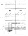
- FIG. 1depicts desired tensile and compressive stress for an N type device and a P type device, respectively;
- FIGS. 2 to 7depict sequential phases of the method according to an embodiment of the invention.
- FIG. 8depicts a top view of a semiconductor device shown in FIG. 3 after the first mask is removed and the second mask is formed thereon to expose a PMOS region according to an embodiment of the invention.
- the inventionintroduces a method for increasing device performances for both an N type device and a P type device, which is easily integrated into conventional processing steps without significantly increasing manufacturing costs. This is achieved by selectively introducing tensile and compressive strains in portions of a semiconductor substrate or layer on which an N type device and a P type device are formed.
- the tensile strainis introduced by expanding a portion of the substrate or layer for the N type device
- the compressive strainis introduced by compressing a portion of the substrate or layer for the P type device.
- FIG. 1illustrates desired stress types for improving the performance of an N type device (e.g., NFET) and a P type device (e.g., PFET).
- N type devicee.g., NFET
- P type devicee.g., PFET
- Each of the NFET and PFEThas a source region, a gate region and a drain region, as shown therein.
- the arrows extending outwardly from the active areaillustrate tensile stress
- the arrows extending inwardly towards the PFET deviceillustrate compressive stress.
- the arrows outwardly extending from the NFET in both the transverse and longitudinal directionsillustrate tensile stress desirable for the NFET.
- the arrows extending inwardly towards the PFET in the longitudinal directionillustrates compressive stress desirable for the PFET.
- the range of stresses needed to influence device drive currentsis of the order of a few hundred MPa to a few GPa.
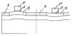
- FIG. 2shows a substrate structure that is divided into an NMOS region and a PMOS region for illustration purposes. Particularly shown is a silicon-on-insulation (SOI) type substrate structure.
- the substrate structurehas a semiconductor substrate 10 , which is typically a silicon substrate, a buried oxide layer 12 formed on the substrate 10 , and a semiconductor layer 14 , which is typically a silicon layer, formed on the buried oxide layer 12 .
- semiconductor substrate 10which is typically a silicon substrate
- a buried oxide layer 12formed on the substrate 10
- a semiconductor layer 14which is typically a silicon layer, formed on the buried oxide layer 12 .
- FIG. 3shallow trench isolation (STI) regions 16 are formed in portions of the semiconductor layer 14 to isolate individual device regions from each other.
- STIshallow trench isolation
- the first mask layer 18is formed on the substrate structure to selectively expose the device region of the NMOS region while masking the PMOS region.
- an expansion elemente.g., O 2
- the ion-implantationis controllably performed such that the implanted expansion element forms the first region 20 in a portion of the substrate 10 underlying the exposed surface portion.
- the concentration peak of the implanted expansion elementis confined within the first region 20 .
- the expansion elementis ion-implanted at an implantation concentration of approximately 1 ⁇ 10 14 atoms/cm 2 to 5 ⁇ 10 16 atoms/cm 2 and at an implantation energy of approximately 30 KeV to 300 KeV.
- the second mask 22is formed thereon to selectively expose the device region of the PMOS region while masking the NMOS region.
- a compression elemente.g., He, Ar or other noble gas
- He, Ar or other noble gasis ion-implanted, onto the exposed surface portion of the semiconductor layer 14 in the PMOS region.
- the ion-implantation processis controllably performed such that the implanted compression element forms a second region 24 in a portion of the substrate underlying the exposed surface portion. Also, the concentration peak of the implanted compression element is confined within the second region 24 .
- the compression elementis ion-implanted at an implantation concentration of approximately 1 ⁇ 10 14 atoms/cm 2 to 5 ⁇ 10 16 atoms/cm 2 and at an implantation energy of approximately 30 KeV to 300 KeV.
- annealingis performed to activate the implanted expansion element and the compression element.
- the first region 20is activated and the expansion element expands the area that was previously occupied by the first region. This occurs through internal oxidation when the implanted O 2 reacts with the silicon and converts to silicon dioxide with its associated volume expansion. This expansion pushes up the portions of the oxide layer 12 and the semiconductor layer 14 overlying the expanded area, thereby increasing tensile stress in the surface portion of the semiconductor layer 14 overlying the expended area.
- the second region 24is activated and the compression element shrinks the area which was previously occupied by the second region. This compression pulls down the portions of the oxide layer 12 and the semiconductor layer 14 overlying the compressed area, thereby increasing compressive stress in the surface portion of the semiconductor layer 14 overlying the compressed area.
- the respective arrows shown in FIG. 6illustrate the regions 22 and 24 being expanding and compressed upon annealing.
- FIG. 7shows gate electrodes 30 formed on the semiconductor layer 14 with a gate oxide layer 28 therebetween in the NMOS area and the PMOS area.
- further processing stepswould include forming N type source and drain regions in the NMOS area to constitute an N type device and P type source and drain regions in the PMOS area to constitute a P type device. Since the N type device is formed on the portion of the semiconductor layer 14 that has tensile strain, the performance of the N type device is significantly improved. Also, due to the compressive strain the performance of the P type device is significantly improved.
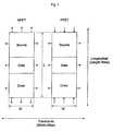
- FIG. 8shows a top view of the substrate structure shown in FIG. 4 prior to ion-implanting the compression element in the PMOS region.
- the dotted lineshows an interface between a device region 32 and the STI region 16 surrounding the device region 32 .
- the second mask 22covers not only the STI region 16 but also portions of the device region 32 except for a center portion of the device region expected to be a channel region for a PMOS device to be formed.
- the compression elementis ion-implanted to an area of the PMOS device region 32 which is smaller than that of the NMOS device region because the strain needed in the PMOS region is preferably only longitudinally compressive as seen in FIG. 1 .
- the inventionenables improving device performance of both an N type device and a P type device by selectively applying tensile stain in the active area, on which an N type device is formed and selectively applying compressive strain in the active region, on which a P type device is formed.
- the tensile strainis created by expanding a portion of the substrate underlying the N type device.
- the expanded portion of the substratepushes up the buried oxide layer and the silicon layer, thereby creating tensile stress to the active region of the silicon layer in the NMOS area.
- the compressed portion of the substratepulls down a portion of the substrate underlying the P type device, thereby creating compressive stress to the active region of the silicon layer in the PMOS area.
- the selective application of tensile strain and compressive strainis obtained by using readily available processing steps. Especially, since only two additional photolithography steps are required for the masking steps, the invention achieves significant improvement in device performance without significant increase in manufacturing costs.
Landscapes
- Engineering & Computer Science (AREA)
- Physics & Mathematics (AREA)
- Condensed Matter Physics & Semiconductors (AREA)
- General Physics & Mathematics (AREA)
- Manufacturing & Machinery (AREA)
- Computer Hardware Design (AREA)
- Microelectronics & Electronic Packaging (AREA)
- Power Engineering (AREA)
- Metal-Oxide And Bipolar Metal-Oxide Semiconductor Integrated Circuits (AREA)
- Element Separation (AREA)
Abstract
Description
This application is a continuation application of U.S. application Ser. No. 10/605,167, filed on Sep. 12, 2003, now U.S. Pat. No. 6,887,751 which is now incorporated herein by reference in its entirety.
1. Field of the Invention
The invention generally relates to methods for manufacturing a semiconductor device with improved device performance, and more particularly to methods for manufacturing semiconductor devices by imposing tensile and compressive stresses in the substrate.
2. Background Description
Mechanical stresses (e.g., tensile stress and compressive stress) within a semiconductor substrate can modulate device performance, which means stresses within a semiconductor substrate enhance semiconductor device characteristics. Thus, the characteristics of a semiconductor device can be improved by creating tensile and/or compressive stresses in the channel regions of an N type device (e.g., NFET) and/or a P type device (e.g., PFET). However, the same stress component, either tensile or compressive stress, discriminatively affects the characteristics of an N type device and a P type device. For example, when tensile stress is applied to a device in the direction of current flow, the performance of an N type device is enhanced but the performance of a P type device is degraded. Thus, in order to maximize the performance of both N type and P type devices formed on the same semiconductor substrate, each stress component should be selectively engineered and applied to either NFETs or PFETs.
To selectively create tensile stress to an N type device and compressive stress to a P type device, respectively, distinctive processes and different combinations of materials are used. For example, a trench isolation structure can be used in forming N type and P type devices. When the trench isolation structure is formed, an isolation region for the N type device contains the isolation material which applies appropriate stress to the N type device in a longitudinal direction and in a transverse direction. Further, the first isolation region and the second isolation region are provided for the P type, which apply a unique mechanical stress on the P type device in the longitudinal direction.
Alternatively, liners can be formed on the side surfaces of a gate electrode, to selectively induce appropriate stress types in the channels of the N type or P type devices. By providing liners, it is possible to apply appropriate stress closer to the device than relying on the trench isolation fill technique.
While these methods enables selectively applying tensile stress to the N type device and compressive stress to the PFET device along the longitudinal direction, they require more complicated processing steps and specific materials, thereby increasing manufacturing costs. Further, only a moderate amount of stress is obtained, such as only in the order of hundreds of MPa.
Therefore, there is a need for more cost effective and cost-effective methodology for creating larger amounts of tensile and compressive stresses for both N type and P type devices without departing from readily available processing techniques.
In an aspect of the invention, a method for manufacturing a semiconductor device is provided. The method includes forming a semiconductor layer on a substrate. The first region of the substrate is expanded to push up the first portion of the semiconductor layer. The second region of the substrate is shrunk or compressed to pull down the second portion of the semiconductor layer. An N type device is formed over the first portion of the semiconductor layer. A P type device is formed over the second portion of the semiconductor layer.
In another aspect of the invention, a method of manufacturing a semiconductor device is provided. A semiconductor layer is formed on a substrate. An expansion element is selectively ion-implanted in the first region of the substrate. A compression element is selectively ion-implanted in the second region of the substrate. Annealing is performed to expand the first region and to shrink or compress the second region. The expanded first portion pushes up the first portion of the semiconductor layer and the compressed second portion pulls down the second portion of the semiconductor layer. An N type device is formed on the first portion of the semiconductor layer. A P type device is formed on the second portion of the semiconductor layer.
Yet another aspect of the invention is a semiconductor having a substrate comprising an expanded region and a compressed region. A semiconductor layer is formed on the substrate and have the first portion pushed up by the expanded region and the second portion pulled down by the compressed region. An N type device is formed on the first portion, and a P type device formed on the second portion.
The invention introduces a method for increasing device performances for both an N type device and a P type device, which is easily integrated into conventional processing steps without significantly increasing manufacturing costs. This is achieved by selectively introducing tensile and compressive strains in portions of a semiconductor substrate or layer on which an N type device and a P type device are formed. In general, the tensile strain is introduced by expanding a portion of the substrate or layer for the N type device, and the compressive strain is introduced by compressing a portion of the substrate or layer for the P type device.
As shown inFIG. 4 , the first mask layer18 is formed on the substrate structure to selectively expose the device region of the NMOS region while masking the PMOS region. Subsequently, an expansion element (e.g., O2) is ion-implanted, as shown by arrows “A”, onto the exposed surface portion of thesemiconductor layer 14 in the NMOS region. The ion-implantation is controllably performed such that the implanted expansion element forms thefirst region 20 in a portion of the substrate10 underlying the exposed surface portion. Also, the concentration peak of the implanted expansion element is confined within thefirst region 20. In an embodiment, the expansion element is ion-implanted at an implantation concentration of approximately 1×10¹⁴atoms/cm2to 5×10¹⁶atoms/cm2and at an implantation energy of approximately 30 KeV to 300 KeV.
After removing the first mask18 from the substrate structure, as shown inFIG. 5 , thesecond mask 22 is formed thereon to selectively expose the device region of the PMOS region while masking the NMOS region. Subsequently, as shown by arrows “B”, a compression element (e.g., He, Ar or other noble gas) is ion-implanted, onto the exposed surface portion of thesemiconductor layer 14 in the PMOS region.
The ion-implantation process is controllably performed such that the implanted compression element forms asecond region 24 in a portion of the substrate underlying the exposed surface portion. Also, the concentration peak of the implanted compression element is confined within thesecond region 24. In an embodiment, the compression element is ion-implanted at an implantation concentration of approximately 1×10¹⁴atoms/cm2to 5×10¹⁶atoms/cm2and at an implantation energy of approximately 30 KeV to 300 KeV.
Upon forming thefirst region 20 containing the expansion element and thesecond region 24 containing the compression element, annealing is performed to activate the implanted expansion element and the compression element. As shown inFIG. 6 , when annealing is performed, thefirst region 20 is activated and the expansion element expands the area that was previously occupied by the first region. This occurs through internal oxidation when the implanted O2reacts with the silicon and converts to silicon dioxide with its associated volume expansion. This expansion pushes up the portions of the oxide layer12 and thesemiconductor layer 14 overlying the expanded area, thereby increasing tensile stress in the surface portion of thesemiconductor layer 14 overlying the expended area.
Also, upon annealing, thesecond region 24 is activated and the compression element shrinks the area which was previously occupied by the second region. This compression pulls down the portions of the oxide layer12 and thesemiconductor layer 14 overlying the compressed area, thereby increasing compressive stress in the surface portion of thesemiconductor layer 14 overlying the compressed area. The respective arrows shown inFIG. 6 illustrate theregions
Thus, according to an embodiment of the invention, the compression element is ion-implanted to an area of the PMOS device region32 which is smaller than that of the NMOS device region because the strain needed in the PMOS region is preferably only longitudinally compressive as seen inFIG. 1 .
As explained above, the invention enables improving device performance of both an N type device and a P type device by selectively applying tensile stain in the active area, on which an N type device is formed and selectively applying compressive strain in the active region, on which a P type device is formed.
The tensile strain is created by expanding a portion of the substrate underlying the N type device. The expanded portion of the substrate pushes up the buried oxide layer and the silicon layer, thereby creating tensile stress to the active region of the silicon layer in the NMOS area. The compressed portion of the substrate pulls down a portion of the substrate underlying the P type device, thereby creating compressive stress to the active region of the silicon layer in the PMOS area.
The selective application of tensile strain and compressive strain is obtained by using readily available processing steps. Especially, since only two additional photolithography steps are required for the masking steps, the invention achieves significant improvement in device performance without significant increase in manufacturing costs.
While the invention has been described in terms of embodiments, those skilled in the art will recognize that the invention can be practiced with modification within the spirit and scope of the appended claims.
Claims (19)
1. A method for manufacturing a semiconductor device, comprising steps of:
forming a buried oxide layer on a silicon substrate;
forming a semiconductor layer on the buried oxide layer such that the buried oxide layer is disposed between the semiconductor layer and the substrate;
performing a first ion-implanting step of an expansion element in a first region of the substrate while masking a second region of the substrate;
performing a second ion-implanting step of a compression element in the second region of the substrate while masking the first region of the substrate, wherein the second ion-implanting step is separate from the first ion-implanting step;
expanding the expansion element to expand the first region of the substrate to push up a first portion of the semiconductor layer and a first portion of the buried oxide layer;
compressing the compression element to compress the second region of the substrate to pull down a second portion of the semiconductor layer and a second portion of the buried oxide layer;
forming a first gate oxide layer of an N type device on the first portion of the semiconductor layer;
forming a first gate electrode on the first gate oxide layer;
forming a second gate oxide layer of a P type device on the second portion of the semiconductor layer; and
forming a second gate electrode on the second gate oxide layer.
2. The method ofclaim 1 , wherein the step of expanding the first region comprises a step of ion-implanting the expansion element in the first region of the substrate.
3. The method ofclaim 2 , wherein the expansion element is ion-implanted at an implantation concentration of approximately 1×10¹⁴atoms/cm2to 5×10¹⁶atoms/cm2and at an implantation energy of approximately 30 KeV to 300 KeV.
4. The method ofclaim 2 , wherein a concentration peak of the implanted expansion element is confined within the first region.
5. The method ofclaim 3 , wherein the expansion element is O2.
6. The method ofclaim 1 , wherein the step of compressing the second region comprises a step of ion-implanting the compression element in the second region of the substrate.
7. The method ofclaim 6 , wherein the compression element is ion-implanted at an implantation concentration of approximately 1×10¹⁴atoms/cm2to 5 ×10¹⁶atoms/cm2at an implantation energy of approximately 30 KeV to 300 KeV.
8. The method ofclaim 6 , wherein a concentration peak of the implanted compression element is confined within the second region.
9. The method ofclaim 6 , wherein the compression element is He, Ar, or noble gas.
10. A method for manufacturing a semiconductor device, comprising steps of:
forming a buried oxide layer on a silicon substrate;
forming a semiconductor layer on the buried oxide layer, wherein the buried oxide layer is disposed between the semiconductor layer and the substrate;
performing a first ion-implanting step of an expansion element in a first region of the substrate while masking a second region of the substrate;
performing a second ion-implanting step of a compression element in the second region of the substrate while masking the first region of the substrate, wherein the second ion-implanting step is separate from the first ion-implanting step;
expanding the expansion element to expand the first region of the substrate to provide a tensile stress in the semiconductor layer;
compressing the second region of the substrate to provide a compressive stress in the semiconductor layer by annealing to activate the compression element;
after the expanding, forming a first gate oxide layer of an N type device on the semiconductor layer over the first region of the substrate;
forming a first gate electrode on the first gate oxide layer;
after the compressing, forming a second gate oxide layer of a P type device on the semiconductor layer over the second region of the substrate; and
forming a second gate electrode on the second gate oxide layer,
wherein the expanding pushes up a first portion of the buried oxide layer; and
the compressing pulls down a second portion of the buried oxide layer.
11. The method ofclaim 10 , wherein the compression element is ion-implanted at an implantation concentration of approximately 1×10 atoms/cm2to 5×10¹⁶atoms/cm2and at an implantation energy of approximately 30 KeV to 300 KeV.
12. The method ofclaim 10 , wherein the step of expanding the first region comprises a step of ion-implanting the expansion element in the first region of the substrate.
13. The method ofclaim 12 , wherein the expansion element is ion-implanted at an implantation concentration of approximately 1×10¹⁴atoms/cm2to 5×10¹⁶atoms/cm2and at an implantation energy of approximately 30 KeV to 300 KeV.
14. The method ofclaim 12 , wherein the expansion element is O2and the compression element is He, Ar, or noble gas.
15. The method ofclaim 1 , wherein:
the step of expanding the first region comprises ion-implanting the expansion element in the first region of the substrate and annealing to activate the expansion element; and
the step of compressing the second region comprises ion-implanting the compression element in the second region of the substrate and annealing to activate the compression element.
16. The method ofclaim 15 , wherein
the expanding the first region pushes up the first portion of the buried oxide layer and the first portion of the semiconductor layer thereby increasing tensile stress in the first portion if the semiconductor layer, and
the compressing the second region pulls down the second portion of the buried oxide layer and the second portion of the semiconductor layer thereby increasing the compressive stress in the second portion of the semiconductor layer.
17. The method ofclaim 10 , wherein the step of expanding the first region comprises ion-implanting the expansion element in the first region of the substrate and annealing to activate the expansion element.
18. The method ofclaim 17 , wherein
the expanding the first region pushes up the first portion of the buried oxide layer and a first portion of the semiconductor layer thereby increasing tensile stress in the first portion of the semiconductor layer, and
the compressing the second region pulls down the second portion of the buried oxide layer and a second portion of the semiconductor layer thereby increasing the compressive stress in the second portion of the semiconductor layer.
19. The method ofclaim 1 , further comprising:
forming a shallow trench isolation region in the semiconductor layer between the first portion of the semiconductor layer and the second portion of the semiconductor layer; and
annealing to activate the expansion element and the compression element, wherein the annealing causes the expanding and the compressing;
wherein the performing the first ion-implanting step comprises:
forming a first mask layer on the semiconductor layer, wherein the first mask layer selectively exposes the first portion of the semiconductor layer and masks the second portion of the semiconductor layer;
ion-implanting the expansion element through an opening in the first mask layer, through the semiconductor layer, through the buried oxide layer, and into the first region of the substrate; and
removing the first mask layer;
the performing the second ion-implanting step comprises:
forming a second mask layer on the semiconductor layer, wherein the second mask layer selectively exposes the second portion of the semiconductor layer and masks the first portion of the semiconductor layer;
ion-implanting the compression element through an opening in the second mask layer, through the semiconductor layer, through the buried oxide layer, and into the second region of the substrate; and
removing the second mask layer;
the forming the first gate oxide layer is performed after the expanding, such that the first portion of the semiconductor layer and the first portion of the buried oxide layer are pushed up prior to the first gate oxide layer being formed; and
the forming the second gate oxide layer is performed after the compressing, such that the second portion of the semiconductor layer and the second portion of the buried oxide layer are pulled down prior to the second gate oxide layer being formed.
Priority Applications (1)
| Application Number | Priority Date | Filing Date | Title |
|---|---|---|---|
| US11/065,061US7745277B2 (en) | 2003-09-12 | 2005-02-25 | MOSFET performance improvement using deformation in SOI structure |
Applications Claiming Priority (2)
| Application Number | Priority Date | Filing Date | Title |
|---|---|---|---|
| US10/605,167US6887751B2 (en) | 2003-09-12 | 2003-09-12 | MOSFET performance improvement using deformation in SOI structure |
| US11/065,061US7745277B2 (en) | 2003-09-12 | 2005-02-25 | MOSFET performance improvement using deformation in SOI structure |
Related Parent Applications (1)
| Application Number | Title | Priority Date | Filing Date |
|---|---|---|---|
| US10/605,167DivisionUS6887751B2 (en) | 2003-09-12 | 2003-09-12 | MOSFET performance improvement using deformation in SOI structure |
Publications (2)
| Publication Number | Publication Date |
|---|---|
| US20050142788A1 US20050142788A1 (en) | 2005-06-30 |
| US7745277B2true US7745277B2 (en) | 2010-06-29 |
Family
ID=34273160
Family Applications (2)
| Application Number | Title | Priority Date | Filing Date |
|---|---|---|---|
| US10/605,167Expired - Fee RelatedUS6887751B2 (en) | 2003-09-12 | 2003-09-12 | MOSFET performance improvement using deformation in SOI structure |
| US11/065,061Expired - Fee RelatedUS7745277B2 (en) | 2003-09-12 | 2005-02-25 | MOSFET performance improvement using deformation in SOI structure |
Family Applications Before (1)
| Application Number | Title | Priority Date | Filing Date |
|---|---|---|---|
| US10/605,167Expired - Fee RelatedUS6887751B2 (en) | 2003-09-12 | 2003-09-12 | MOSFET performance improvement using deformation in SOI structure |
Country Status (1)
| Country | Link |
|---|---|
| US (2) | US6887751B2 (en) |
Cited By (1)
| Publication number | Priority date | Publication date | Assignee | Title |
|---|---|---|---|---|
| US9515181B2 (en) | 2014-08-06 | 2016-12-06 | Qualcomm Incorporated | Semiconductor device with self-aligned back side features |
Families Citing this family (46)
| Publication number | Priority date | Publication date | Assignee | Title |
|---|---|---|---|---|
| US6887751B2 (en)* | 2003-09-12 | 2005-05-03 | International Business Machines Corporation | MOSFET performance improvement using deformation in SOI structure |
| US7319258B2 (en)* | 2003-10-31 | 2008-01-15 | Taiwan Semiconductor Manufacturing Company, Ltd. | Semiconductor-on-insulator chip with<100>-oriented transistors |
| US8450806B2 (en)* | 2004-03-31 | 2013-05-28 | International Business Machines Corporation | Method for fabricating strained silicon-on-insulator structures and strained silicon-on insulator structures formed thereby |
| US7462522B2 (en)* | 2006-08-30 | 2008-12-09 | International Business Machines Corporation | Method and structure for improving device performance variation in dual stress liner technology |
| US7829407B2 (en) | 2006-11-20 | 2010-11-09 | International Business Machines Corporation | Method of fabricating a stressed MOSFET by bending SOI region |
| US8569858B2 (en) | 2006-12-20 | 2013-10-29 | Freescale Semiconductor, Inc. | Semiconductor device including an active region and two layers having different stress characteristics |
| DE102008006961A1 (en)* | 2008-01-31 | 2009-08-27 | Advanced Micro Devices, Inc., Sunnyvale | A method of creating a deformed channel region in a transistor by deep implantation of a strain inducing species under the channel region |
| US20100017431A1 (en)* | 2008-06-25 | 2010-01-21 | Martin Schmidt | Methods and Systems for Social Networking |
| US10833194B2 (en) | 2010-08-27 | 2020-11-10 | Acorn Semi, Llc | SOI wafers and devices with buried stressor |
| US8466502B2 (en) | 2011-03-24 | 2013-06-18 | United Microelectronics Corp. | Metal-gate CMOS device |
| US8445363B2 (en) | 2011-04-21 | 2013-05-21 | United Microelectronics Corp. | Method of fabricating an epitaxial layer |
| US8324059B2 (en) | 2011-04-25 | 2012-12-04 | United Microelectronics Corp. | Method of fabricating a semiconductor structure |
| US8426284B2 (en) | 2011-05-11 | 2013-04-23 | United Microelectronics Corp. | Manufacturing method for semiconductor structure |
| US8481391B2 (en) | 2011-05-18 | 2013-07-09 | United Microelectronics Corp. | Process for manufacturing stress-providing structure and semiconductor device with such stress-providing structure |
| US8431460B2 (en) | 2011-05-27 | 2013-04-30 | United Microelectronics Corp. | Method for fabricating semiconductor device |
| US8716750B2 (en) | 2011-07-25 | 2014-05-06 | United Microelectronics Corp. | Semiconductor device having epitaxial structures |
| US8575043B2 (en) | 2011-07-26 | 2013-11-05 | United Microelectronics Corp. | Semiconductor device and manufacturing method thereof |
| US8647941B2 (en) | 2011-08-17 | 2014-02-11 | United Microelectronics Corp. | Method of forming semiconductor device |
| US8674433B2 (en) | 2011-08-24 | 2014-03-18 | United Microelectronics Corp. | Semiconductor process |
| US8476169B2 (en) | 2011-10-17 | 2013-07-02 | United Microelectronics Corp. | Method of making strained silicon channel semiconductor structure |
| US8691659B2 (en) | 2011-10-26 | 2014-04-08 | United Microelectronics Corp. | Method for forming void-free dielectric layer |
| US8754448B2 (en) | 2011-11-01 | 2014-06-17 | United Microelectronics Corp. | Semiconductor device having epitaxial layer |
| US8647953B2 (en) | 2011-11-17 | 2014-02-11 | United Microelectronics Corp. | Method for fabricating first and second epitaxial cap layers |
| US8709930B2 (en) | 2011-11-25 | 2014-04-29 | United Microelectronics Corp. | Semiconductor process |
| US9136348B2 (en) | 2012-03-12 | 2015-09-15 | United Microelectronics Corp. | Semiconductor structure and fabrication method thereof |
| US9202914B2 (en) | 2012-03-14 | 2015-12-01 | United Microelectronics Corporation | Semiconductor device and method for fabricating the same |
| US8664069B2 (en) | 2012-04-05 | 2014-03-04 | United Microelectronics Corp. | Semiconductor structure and process thereof |
| CN103377930B (en)* | 2012-04-19 | 2015-11-25 | 中国科学院微电子研究所 | Semiconductor structure and manufacturing method thereof |
| US8866230B2 (en) | 2012-04-26 | 2014-10-21 | United Microelectronics Corp. | Semiconductor devices |
| US8835243B2 (en) | 2012-05-04 | 2014-09-16 | United Microelectronics Corp. | Semiconductor process |
| US8951876B2 (en) | 2012-06-20 | 2015-02-10 | United Microelectronics Corp. | Semiconductor device and manufacturing method thereof |
| US8796695B2 (en) | 2012-06-22 | 2014-08-05 | United Microelectronics Corp. | Multi-gate field-effect transistor and process thereof |
| US8710632B2 (en) | 2012-09-07 | 2014-04-29 | United Microelectronics Corp. | Compound semiconductor epitaxial structure and method for fabricating the same |
| CN103811349A (en)* | 2012-11-06 | 2014-05-21 | 中国科学院微电子研究所 | Semiconductor structure and manufacturing method thereof |
| US9117925B2 (en) | 2013-01-31 | 2015-08-25 | United Microelectronics Corp. | Epitaxial process |
| US8753902B1 (en) | 2013-03-13 | 2014-06-17 | United Microelectronics Corp. | Method of controlling etching process for forming epitaxial structure |
| US9034705B2 (en) | 2013-03-26 | 2015-05-19 | United Microelectronics Corp. | Method of forming semiconductor device |
| US9064893B2 (en) | 2013-05-13 | 2015-06-23 | United Microelectronics Corp. | Gradient dopant of strained substrate manufacturing method of semiconductor device |
| US8853060B1 (en) | 2013-05-27 | 2014-10-07 | United Microelectronics Corp. | Epitaxial process |
| US9076652B2 (en) | 2013-05-27 | 2015-07-07 | United Microelectronics Corp. | Semiconductor process for modifying shape of recess |
| US8765546B1 (en) | 2013-06-24 | 2014-07-01 | United Microelectronics Corp. | Method for fabricating fin-shaped field-effect transistor |
| US8895396B1 (en) | 2013-07-11 | 2014-11-25 | United Microelectronics Corp. | Epitaxial Process of forming stress inducing epitaxial layers in source and drain regions of PMOS and NMOS structures |
| US8981487B2 (en) | 2013-07-31 | 2015-03-17 | United Microelectronics Corp. | Fin-shaped field-effect transistor (FinFET) |
| US9306066B2 (en) | 2014-02-28 | 2016-04-05 | Qualcomm Incorporated | Method and apparatus of stressed FIN NMOS FinFET |
| US10516050B2 (en) | 2016-07-29 | 2019-12-24 | Taiwan Semiconductor Manufacturing Co., Ltd. | Method for forming stressor, semiconductor device having stressor, and method for forming the same |
| WO2018136896A1 (en)* | 2017-01-23 | 2018-07-26 | Acorn Technologies, Inc. | Strained semiconductor-on-insulator by deformation of buried insulator induced by buried stressor |
Citations (93)
| Publication number | Priority date | Publication date | Assignee | Title |
|---|---|---|---|---|
| US3602841A (en) | 1970-06-18 | 1971-08-31 | Ibm | High frequency bulk semiconductor amplifiers and oscillators |
| US4665415A (en) | 1985-04-24 | 1987-05-12 | International Business Machines Corporation | Semiconductor device with hole conduction via strained lattice |
| US4853076A (en) | 1983-12-29 | 1989-08-01 | Massachusetts Institute Of Technology | Semiconductor thin films |
| US4855245A (en) | 1985-09-13 | 1989-08-08 | Siemens Aktiengesellschaft | Method of manufacturing integrated circuit containing bipolar and complementary MOS transistors on a common substrate |
| US4952524A (en) | 1989-05-05 | 1990-08-28 | At&T Bell Laboratories | Semiconductor device manufacture including trench formation |
| US4958213A (en) | 1987-12-07 | 1990-09-18 | Texas Instruments Incorporated | Method for forming a transistor base region under thick oxide |
| US5006913A (en) | 1988-11-05 | 1991-04-09 | Mitsubishi Denki Kabushiki Kaisha | Stacked type semiconductor device |
| US5060030A (en) | 1990-07-18 | 1991-10-22 | Raytheon Company | Pseudomorphic HEMT having strained compensation layer |
| US5081513A (en) | 1991-02-28 | 1992-01-14 | Xerox Corporation | Electronic device with recovery layer proximate to active layer |
| US5108843A (en) | 1988-11-30 | 1992-04-28 | Ricoh Company, Ltd. | Thin film semiconductor and process for producing the same |
| US5134085A (en) | 1991-11-21 | 1992-07-28 | Micron Technology, Inc. | Reduced-mask, split-polysilicon CMOS process, incorporating stacked-capacitor cells, for fabricating multi-megabit dynamic random access memories |
| US5310446A (en) | 1990-01-10 | 1994-05-10 | Ricoh Company, Ltd. | Method for producing semiconductor film |
| US5354695A (en) | 1992-04-08 | 1994-10-11 | Leedy Glenn J | Membrane dielectric isolation IC fabrication |
| US5371399A (en) | 1991-06-14 | 1994-12-06 | International Business Machines Corporation | Compound semiconductor having metallic inclusions and devices fabricated therefrom |
| US5391510A (en) | 1992-02-28 | 1995-02-21 | International Business Machines Corporation | Formation of self-aligned metal gate FETs using a benignant removable gate material during high temperature steps |
| US5459346A (en) | 1988-06-28 | 1995-10-17 | Ricoh Co., Ltd. | Semiconductor substrate with electrical contact in groove |
| US5557122A (en) | 1995-05-12 | 1996-09-17 | Alliance Semiconductors Corporation | Semiconductor electrode having improved grain structure and oxide growth properties |
| US5561302A (en) | 1994-09-26 | 1996-10-01 | Motorola, Inc. | Enhanced mobility MOSFET device and method |
| US5670798A (en) | 1995-03-29 | 1997-09-23 | North Carolina State University | Integrated heterostructures of Group III-V nitride semiconductor materials including epitaxial ohmic contact non-nitride buffer layer and methods of fabricating same |
| US5679965A (en) | 1995-03-29 | 1997-10-21 | North Carolina State University | Integrated heterostructures of Group III-V nitride semiconductor materials including epitaxial ohmic contact, non-nitride buffer layer and methods of fabricating same |
| US5861651A (en) | 1997-02-28 | 1999-01-19 | Lucent Technologies Inc. | Field effect devices and capacitors with improved thin film dielectrics and method for making same |
| US5880040A (en) | 1996-04-15 | 1999-03-09 | Macronix International Co., Ltd. | Gate dielectric based on oxynitride grown in N2 O and annealed in NO |
| US5940736A (en) | 1997-03-11 | 1999-08-17 | Lucent Technologies Inc. | Method for forming a high quality ultrathin gate oxide layer |
| US5960297A (en) | 1997-07-02 | 1999-09-28 | Kabushiki Kaisha Toshiba | Shallow trench isolation structure and method of forming the same |
| US5989978A (en) | 1998-07-16 | 1999-11-23 | Chartered Semiconductor Manufacturing, Ltd. | Shallow trench isolation of MOSFETS with reduced corner parasitic currents |
| US6008126A (en) | 1992-04-08 | 1999-12-28 | Elm Technology Corporation | Membrane dielectric isolation IC fabrication |
| US6025280A (en) | 1997-04-28 | 2000-02-15 | Lucent Technologies Inc. | Use of SiD4 for deposition of ultra thin and controllable oxides |
| US6066545A (en) | 1997-12-09 | 2000-05-23 | Texas Instruments Incorporated | Birdsbeak encroachment using combination of wet and dry etch for isolation nitride |
| US6090684A (en) | 1998-07-31 | 2000-07-18 | Hitachi, Ltd. | Method for manufacturing semiconductor device |
| US6107143A (en) | 1998-03-02 | 2000-08-22 | Samsung Electronics Co., Ltd. | Method for forming a trench isolation structure in an integrated circuit |
| US6117722A (en) | 1999-02-18 | 2000-09-12 | Taiwan Semiconductor Manufacturing Company | SRAM layout for relaxing mechanical stress in shallow trench isolation technology and method of manufacture thereof |
| US6133071A (en) | 1997-10-15 | 2000-10-17 | Nec Corporation | Semiconductor device with plate heat sink free from cracks due to thermal stress and process for assembling it with package |
| US6165383A (en) | 1998-04-10 | 2000-12-26 | Organic Display Technology | Useful precursors for organic electroluminescent materials and devices made from such materials |
| US6221735B1 (en) | 2000-02-15 | 2001-04-24 | Philips Semiconductors, Inc. | Method for eliminating stress induced dislocations in CMOS devices |
| US6228694B1 (en) | 1999-06-28 | 2001-05-08 | Intel Corporation | Method of increasing the mobility of MOS transistors by use of localized stress regions |
| US6255169B1 (en) | 1999-02-22 | 2001-07-03 | Advanced Micro Devices, Inc. | Process for fabricating a high-endurance non-volatile memory device |
| US6261876B1 (en) | 1999-11-04 | 2001-07-17 | International Business Machines Corporation | Planar mixed SOI-bulk substrate for microelectronic applications |
| US6261964B1 (en) | 1997-03-14 | 2001-07-17 | Micron Technology, Inc. | Material removal method for forming a structure |
| US6265317B1 (en) | 2001-01-09 | 2001-07-24 | Taiwan Semiconductor Manufacturing Company | Top corner rounding for shallow trench isolation |
| US20010009784A1 (en) | 1998-01-09 | 2001-07-26 | Yanjun Ma | Structure and method of making a sub-micron MOS transistor |
| US6274444B1 (en) | 1999-07-30 | 2001-08-14 | United Microelectronics Corp. | Method for forming mosfet |
| US6281532B1 (en) | 1999-06-28 | 2001-08-28 | Intel Corporation | Technique to obtain increased channel mobilities in NMOS transistors by gate electrode engineering |
| US6284623B1 (en) | 1999-10-25 | 2001-09-04 | Peng-Fei Zhang | Method of fabricating semiconductor devices using shallow trench isolation with reduced narrow channel effect |
| US6284626B1 (en) | 1999-04-06 | 2001-09-04 | Vantis Corporation | Angled nitrogen ion implantation for minimizing mechanical stress on side walls of an isolation trench |
| US6319794B1 (en) | 1998-10-14 | 2001-11-20 | International Business Machines Corporation | Structure and method for producing low leakage isolation devices |
| US6361885B1 (en) | 1998-04-10 | 2002-03-26 | Organic Display Technology | Organic electroluminescent materials and device made from such materials |
| US6362082B1 (en) | 1999-06-28 | 2002-03-26 | Intel Corporation | Methodology for control of short channel effects in MOS transistors |
| US6368931B1 (en) | 2000-03-27 | 2002-04-09 | Intel Corporation | Thin tensile layers in shallow trench isolation and method of making same |
| US20020063292A1 (en) | 2000-11-29 | 2002-05-30 | Mark Armstrong | CMOS fabrication process utilizing special transistor orientation |
| US6403975B1 (en) | 1996-04-09 | 2002-06-11 | Max-Planck Gesellschaft Zur Forderung Der Wissenschafteneev | Semiconductor components, in particular photodetectors, light emitting diodes, optical modulators and waveguides with multilayer structures grown on silicon substrates |
| US6403486B1 (en) | 2001-04-30 | 2002-06-11 | Taiwan Semiconductor Manufacturing Company | Method for forming a shallow trench isolation |
| US6406973B1 (en) | 1999-06-29 | 2002-06-18 | Hyundai Electronics Industries Co., Ltd. | Transistor in a semiconductor device and method of manufacturing the same |
| US20020086472A1 (en) | 2000-12-29 | 2002-07-04 | Brian Roberds | Technique to obtain high mobility channels in MOS transistors by forming a strain layer on an underside of a channel |
| US20020086497A1 (en) | 2000-12-30 | 2002-07-04 | Kwok Siang Ping | Beaker shape trench with nitride pull-back for STI |
| US20020090791A1 (en) | 1999-06-28 | 2002-07-11 | Brian S. Doyle | Method for reduced capacitance interconnect system using gaseous implants into the ild |
| US6461936B1 (en) | 2002-01-04 | 2002-10-08 | Infineon Technologies Ag | Double pullback method of filling an isolation trench |
| US6476462B2 (en) | 1999-12-28 | 2002-11-05 | Texas Instruments Incorporated | MOS-type semiconductor device and method for making same |
| US6483171B1 (en) | 1999-08-13 | 2002-11-19 | Micron Technology, Inc. | Vertical sub-micron CMOS transistors on (110), (111), (311), (511), and higher order surfaces of bulk, SOI and thin film structures and method of forming same |
| US6493497B1 (en) | 2000-09-26 | 2002-12-10 | Motorola, Inc. | Electro-optic structure and process for fabricating same |
| US6498358B1 (en) | 2001-07-20 | 2002-12-24 | Motorola, Inc. | Structure and method for fabricating an electro-optic system having an electrochromic diffraction grating |
| US6501121B1 (en) | 2000-11-15 | 2002-12-31 | Motorola, Inc. | Semiconductor structure |
| US6506652B2 (en) | 1998-11-13 | 2003-01-14 | Intel Corporation | Method of recessing spacers to improved salicide resistance on polysilicon gates |
| US20030032261A1 (en) | 2001-08-08 | 2003-02-13 | Ling-Yen Yeh | Method of preventing threshold voltage of MOS transistor from being decreased by shallow trench isolation formation |
| US20030040158A1 (en) | 2001-08-21 | 2003-02-27 | Nec Corporation | Semiconductor device and method of fabricating the same |
| US6531369B1 (en) | 2000-03-01 | 2003-03-11 | Applied Micro Circuits Corporation | Heterojunction bipolar transistor (HBT) fabrication using a selectively deposited silicon germanium (SiGe) |
| US6531740B2 (en) | 2001-07-17 | 2003-03-11 | Motorola, Inc. | Integrated impedance matching and stability network |
| US20030057184A1 (en) | 2001-09-22 | 2003-03-27 | Shiuh-Sheng Yu | Method for pull back SiN to increase rounding effect in a shallow trench isolation process |
| US20030067035A1 (en) | 2001-09-28 | 2003-04-10 | Helmut Tews | Gate processing method with reduced gate oxide corner and edge thinning |
| US20030111699A1 (en)* | 2001-12-14 | 2003-06-19 | Christoph Wasshuber | Methods and apparatus for inducing stress in a semiconductor device |
| US6621392B1 (en) | 2002-04-25 | 2003-09-16 | International Business Machines Corporation | Micro electromechanical switch having self-aligned spacers |
| US6635506B2 (en) | 2001-11-07 | 2003-10-21 | International Business Machines Corporation | Method of fabricating micro-electromechanical switches on CMOS compatible substrates |
| US6717216B1 (en) | 2002-12-12 | 2004-04-06 | International Business Machines Corporation | SOI based field effect transistor having a compressive film in undercut area under the channel and a method of making the device |
| US6727549B1 (en)* | 1998-06-30 | 2004-04-27 | Intel Corporation | Method of delaminating a pre-fabricated transistor layer from a substrate for placement on another wafer |
| US6764908B1 (en)* | 2002-06-19 | 2004-07-20 | Advanced Micro Devices, Inc. | Narrow width CMOS devices fabricated on strained lattice semiconductor substrates with maximized NMOS and PMOS drive currents |
| US6790749B2 (en)* | 1992-10-09 | 2004-09-14 | Semiconductor Energy Laboratory Co., Ltd. | Method of manufacturing a semiconductor device |
| US6825529B2 (en) | 2002-12-12 | 2004-11-30 | International Business Machines Corporation | Stress inducing spacers |
| US20040238914A1 (en) | 2003-05-30 | 2004-12-02 | International Business Machines Corporation | STI stress modification by nitrogen plasma treatment for improving performance in small width devices |
| US6831292B2 (en) | 2001-09-21 | 2004-12-14 | Amberwave Systems Corporation | Semiconductor structures employing strained material layers with defined impurity gradients and methods for fabricating same |
| US20040253776A1 (en)* | 2003-06-12 | 2004-12-16 | Thomas Hoffmann | Gate-induced strain for MOS performance improvement |
| US20040262784A1 (en) | 2003-06-30 | 2004-12-30 | International Business Machines Corporation | High performance cmos device structures and method of manufacture |
| US20050037596A1 (en)* | 2003-08-14 | 2005-02-17 | Yuri Erokhin | Internal gettering in SIMOX SOI silicon substrates |
| US20050082634A1 (en) | 2003-10-16 | 2005-04-21 | International Business Machines Corporation | High performance strained cmos devices |
| US6887751B2 (en)* | 2003-09-12 | 2005-05-03 | International Business Machines Corporation | MOSFET performance improvement using deformation in SOI structure |
| US20050093030A1 (en) | 2003-10-30 | 2005-05-05 | Doris Bruce B. | Structure and method to enhance both nFET and pFET performance using different kinds of stressed layers |
| US20050098829A1 (en) | 2003-11-06 | 2005-05-12 | Doris Bruce B. | High mobility CMOS circuits |
| US20050106799A1 (en) | 2003-11-14 | 2005-05-19 | International Business Machines Corporation | Stressed semiconductor device structures having granular semiconductor material |
| US20050145954A1 (en) | 2004-01-05 | 2005-07-07 | International Business Machines Corporation | Structures and methods for making strained mosfets |
| US20050194699A1 (en) | 2004-03-03 | 2005-09-08 | International Business Machines Corporation | Mobility enhanced cmos devices |
| US20050236668A1 (en) | 2004-04-23 | 2005-10-27 | International Business Machines Corporation | STRUCTURES AND METHODS FOR MANUFACTURING OF DISLOCATION FREE STRESSED CHANNELS IN BULK SILICON AND SOI CMOS DEVICES BY GATE STRESS ENGINEERING WITH SiGe AND/OR Si:C |
| US20050245017A1 (en) | 2003-10-30 | 2005-11-03 | Belyansky Michael P | Structure and method to improve channel mobility by gate electrode stress modification |
| US6974981B2 (en) | 2002-12-12 | 2005-12-13 | International Business Machines Corporation | Isolation structures for imposing stress patterns |
| US20060057787A1 (en) | 2002-11-25 | 2006-03-16 | Doris Bruce B | Strained finfet cmos device structures |
| US20060060925A1 (en) | 2004-09-17 | 2006-03-23 | International Business Machines Corporation | Semiconductor device structure with active regions having different surface directions and methods |
- 2003
- 2003-09-12USUS10/605,167patent/US6887751B2/ennot_activeExpired - Fee Related
- 2005
- 2005-02-25USUS11/065,061patent/US7745277B2/ennot_activeExpired - Fee Related
Patent Citations (113)
| Publication number | Priority date | Publication date | Assignee | Title |
|---|---|---|---|---|
| US3602841A (en) | 1970-06-18 | 1971-08-31 | Ibm | High frequency bulk semiconductor amplifiers and oscillators |
| US4853076A (en) | 1983-12-29 | 1989-08-01 | Massachusetts Institute Of Technology | Semiconductor thin films |
| US4665415A (en) | 1985-04-24 | 1987-05-12 | International Business Machines Corporation | Semiconductor device with hole conduction via strained lattice |
| US4855245A (en) | 1985-09-13 | 1989-08-08 | Siemens Aktiengesellschaft | Method of manufacturing integrated circuit containing bipolar and complementary MOS transistors on a common substrate |
| US4958213A (en) | 1987-12-07 | 1990-09-18 | Texas Instruments Incorporated | Method for forming a transistor base region under thick oxide |
| US5459346A (en) | 1988-06-28 | 1995-10-17 | Ricoh Co., Ltd. | Semiconductor substrate with electrical contact in groove |
| US5565697A (en) | 1988-06-28 | 1996-10-15 | Ricoh Company, Ltd. | Semiconductor structure having island forming grooves |
| US5006913A (en) | 1988-11-05 | 1991-04-09 | Mitsubishi Denki Kabushiki Kaisha | Stacked type semiconductor device |
| US5108843A (en) | 1988-11-30 | 1992-04-28 | Ricoh Company, Ltd. | Thin film semiconductor and process for producing the same |
| US4952524A (en) | 1989-05-05 | 1990-08-28 | At&T Bell Laboratories | Semiconductor device manufacture including trench formation |
| US5310446A (en) | 1990-01-10 | 1994-05-10 | Ricoh Company, Ltd. | Method for producing semiconductor film |
| US5060030A (en) | 1990-07-18 | 1991-10-22 | Raytheon Company | Pseudomorphic HEMT having strained compensation layer |
| US5081513A (en) | 1991-02-28 | 1992-01-14 | Xerox Corporation | Electronic device with recovery layer proximate to active layer |
| US5371399A (en) | 1991-06-14 | 1994-12-06 | International Business Machines Corporation | Compound semiconductor having metallic inclusions and devices fabricated therefrom |
| US5471948A (en) | 1991-06-14 | 1995-12-05 | International Business Machines Corporation | Method of making a compound semiconductor having metallic inclusions |
| US5134085A (en) | 1991-11-21 | 1992-07-28 | Micron Technology, Inc. | Reduced-mask, split-polysilicon CMOS process, incorporating stacked-capacitor cells, for fabricating multi-megabit dynamic random access memories |
| US5391510A (en) | 1992-02-28 | 1995-02-21 | International Business Machines Corporation | Formation of self-aligned metal gate FETs using a benignant removable gate material during high temperature steps |
| US5354695A (en) | 1992-04-08 | 1994-10-11 | Leedy Glenn J | Membrane dielectric isolation IC fabrication |
| US5840593A (en) | 1992-04-08 | 1998-11-24 | Elm Technology Corporation | Membrane dielectric isolation IC fabrication |
| US5571741A (en) | 1992-04-08 | 1996-11-05 | Leedy; Glenn J. | Membrane dielectric isolation IC fabrication |
| US5592007A (en) | 1992-04-08 | 1997-01-07 | Leedy; Glenn J. | Membrane dielectric isolation transistor fabrication |
| US5592018A (en) | 1992-04-08 | 1997-01-07 | Leedy; Glenn J. | Membrane dielectric isolation IC fabrication |
| US6008126A (en) | 1992-04-08 | 1999-12-28 | Elm Technology Corporation | Membrane dielectric isolation IC fabrication |
| US5946559A (en) | 1992-04-08 | 1999-08-31 | Elm Technology Corporation | Membrane dielectric isolation IC fabrication |
| US6790749B2 (en)* | 1992-10-09 | 2004-09-14 | Semiconductor Energy Laboratory Co., Ltd. | Method of manufacturing a semiconductor device |
| US5683934A (en) | 1994-09-26 | 1997-11-04 | Motorola, Inc. | Enhanced mobility MOSFET device and method |
| US5561302A (en) | 1994-09-26 | 1996-10-01 | Motorola, Inc. | Enhanced mobility MOSFET device and method |
| US5679965A (en) | 1995-03-29 | 1997-10-21 | North Carolina State University | Integrated heterostructures of Group III-V nitride semiconductor materials including epitaxial ohmic contact, non-nitride buffer layer and methods of fabricating same |
| US5670798A (en) | 1995-03-29 | 1997-09-23 | North Carolina State University | Integrated heterostructures of Group III-V nitride semiconductor materials including epitaxial ohmic contact non-nitride buffer layer and methods of fabricating same |
| US6046464A (en) | 1995-03-29 | 2000-04-04 | North Carolina State University | Integrated heterostructures of group III-V nitride semiconductor materials including epitaxial ohmic contact comprising multiple quantum well |
| US5557122A (en) | 1995-05-12 | 1996-09-17 | Alliance Semiconductors Corporation | Semiconductor electrode having improved grain structure and oxide growth properties |
| US6403975B1 (en) | 1996-04-09 | 2002-06-11 | Max-Planck Gesellschaft Zur Forderung Der Wissenschafteneev | Semiconductor components, in particular photodetectors, light emitting diodes, optical modulators and waveguides with multilayer structures grown on silicon substrates |
| US5880040A (en) | 1996-04-15 | 1999-03-09 | Macronix International Co., Ltd. | Gate dielectric based on oxynitride grown in N2 O and annealed in NO |
| US5861651A (en) | 1997-02-28 | 1999-01-19 | Lucent Technologies Inc. | Field effect devices and capacitors with improved thin film dielectrics and method for making same |
| US5940736A (en) | 1997-03-11 | 1999-08-17 | Lucent Technologies Inc. | Method for forming a high quality ultrathin gate oxide layer |
| US6246095B1 (en) | 1997-03-11 | 2001-06-12 | Agere Systems Guardian Corp. | System and method for forming a uniform thin gate oxide layer |
| US6261964B1 (en) | 1997-03-14 | 2001-07-17 | Micron Technology, Inc. | Material removal method for forming a structure |
| US6025280A (en) | 1997-04-28 | 2000-02-15 | Lucent Technologies Inc. | Use of SiD4 for deposition of ultra thin and controllable oxides |
| US5960297A (en) | 1997-07-02 | 1999-09-28 | Kabushiki Kaisha Toshiba | Shallow trench isolation structure and method of forming the same |
| US6133071A (en) | 1997-10-15 | 2000-10-17 | Nec Corporation | Semiconductor device with plate heat sink free from cracks due to thermal stress and process for assembling it with package |
| US6066545A (en) | 1997-12-09 | 2000-05-23 | Texas Instruments Incorporated | Birdsbeak encroachment using combination of wet and dry etch for isolation nitride |
| US20010009784A1 (en) | 1998-01-09 | 2001-07-26 | Yanjun Ma | Structure and method of making a sub-micron MOS transistor |
| US6107143A (en) | 1998-03-02 | 2000-08-22 | Samsung Electronics Co., Ltd. | Method for forming a trench isolation structure in an integrated circuit |
| US6165383A (en) | 1998-04-10 | 2000-12-26 | Organic Display Technology | Useful precursors for organic electroluminescent materials and devices made from such materials |
| US6361885B1 (en) | 1998-04-10 | 2002-03-26 | Organic Display Technology | Organic electroluminescent materials and device made from such materials |
| US6727549B1 (en)* | 1998-06-30 | 2004-04-27 | Intel Corporation | Method of delaminating a pre-fabricated transistor layer from a substrate for placement on another wafer |
| US5989978A (en) | 1998-07-16 | 1999-11-23 | Chartered Semiconductor Manufacturing, Ltd. | Shallow trench isolation of MOSFETS with reduced corner parasitic currents |
| US6090684A (en) | 1998-07-31 | 2000-07-18 | Hitachi, Ltd. | Method for manufacturing semiconductor device |
| US6319794B1 (en) | 1998-10-14 | 2001-11-20 | International Business Machines Corporation | Structure and method for producing low leakage isolation devices |
| US6521964B1 (en) | 1998-11-13 | 2003-02-18 | Intel Corporation | Device having spacers for improved salicide resistance on polysilicon gates |
| US6509618B2 (en) | 1998-11-13 | 2003-01-21 | Intel Corporation | Device having thin first spacers and partially recessed thick second spacers for improved salicide resistance on polysilicon gates |
| US6506652B2 (en) | 1998-11-13 | 2003-01-14 | Intel Corporation | Method of recessing spacers to improved salicide resistance on polysilicon gates |
| US6117722A (en) | 1999-02-18 | 2000-09-12 | Taiwan Semiconductor Manufacturing Company | SRAM layout for relaxing mechanical stress in shallow trench isolation technology and method of manufacture thereof |
| US6255169B1 (en) | 1999-02-22 | 2001-07-03 | Advanced Micro Devices, Inc. | Process for fabricating a high-endurance non-volatile memory device |
| US6284626B1 (en) | 1999-04-06 | 2001-09-04 | Vantis Corporation | Angled nitrogen ion implantation for minimizing mechanical stress on side walls of an isolation trench |
| US6362082B1 (en) | 1999-06-28 | 2002-03-26 | Intel Corporation | Methodology for control of short channel effects in MOS transistors |
| US20020074598A1 (en) | 1999-06-28 | 2002-06-20 | Doyle Brian S. | Methodology for control of short channel effects in MOS transistors |
| US6228694B1 (en) | 1999-06-28 | 2001-05-08 | Intel Corporation | Method of increasing the mobility of MOS transistors by use of localized stress regions |
| US6281532B1 (en) | 1999-06-28 | 2001-08-28 | Intel Corporation | Technique to obtain increased channel mobilities in NMOS transistors by gate electrode engineering |
| US20020090791A1 (en) | 1999-06-28 | 2002-07-11 | Brian S. Doyle | Method for reduced capacitance interconnect system using gaseous implants into the ild |
| US6406973B1 (en) | 1999-06-29 | 2002-06-18 | Hyundai Electronics Industries Co., Ltd. | Transistor in a semiconductor device and method of manufacturing the same |
| US6274444B1 (en) | 1999-07-30 | 2001-08-14 | United Microelectronics Corp. | Method for forming mosfet |
| US6483171B1 (en) | 1999-08-13 | 2002-11-19 | Micron Technology, Inc. | Vertical sub-micron CMOS transistors on (110), (111), (311), (511), and higher order surfaces of bulk, SOI and thin film structures and method of forming same |
| US6284623B1 (en) | 1999-10-25 | 2001-09-04 | Peng-Fei Zhang | Method of fabricating semiconductor devices using shallow trench isolation with reduced narrow channel effect |
| US6261876B1 (en) | 1999-11-04 | 2001-07-17 | International Business Machines Corporation | Planar mixed SOI-bulk substrate for microelectronic applications |
| US6476462B2 (en) | 1999-12-28 | 2002-11-05 | Texas Instruments Incorporated | MOS-type semiconductor device and method for making same |
| US6221735B1 (en) | 2000-02-15 | 2001-04-24 | Philips Semiconductors, Inc. | Method for eliminating stress induced dislocations in CMOS devices |
| US6531369B1 (en) | 2000-03-01 | 2003-03-11 | Applied Micro Circuits Corporation | Heterojunction bipolar transistor (HBT) fabrication using a selectively deposited silicon germanium (SiGe) |
| US6368931B1 (en) | 2000-03-27 | 2002-04-09 | Intel Corporation | Thin tensile layers in shallow trench isolation and method of making same |
| US6493497B1 (en) | 2000-09-26 | 2002-12-10 | Motorola, Inc. | Electro-optic structure and process for fabricating same |
| US6501121B1 (en) | 2000-11-15 | 2002-12-31 | Motorola, Inc. | Semiconductor structure |
| US20020063292A1 (en) | 2000-11-29 | 2002-05-30 | Mark Armstrong | CMOS fabrication process utilizing special transistor orientation |
| US20020086472A1 (en) | 2000-12-29 | 2002-07-04 | Brian Roberds | Technique to obtain high mobility channels in MOS transistors by forming a strain layer on an underside of a channel |
| US20020086497A1 (en) | 2000-12-30 | 2002-07-04 | Kwok Siang Ping | Beaker shape trench with nitride pull-back for STI |
| US6265317B1 (en) | 2001-01-09 | 2001-07-24 | Taiwan Semiconductor Manufacturing Company | Top corner rounding for shallow trench isolation |
| US6403486B1 (en) | 2001-04-30 | 2002-06-11 | Taiwan Semiconductor Manufacturing Company | Method for forming a shallow trench isolation |
| US6531740B2 (en) | 2001-07-17 | 2003-03-11 | Motorola, Inc. | Integrated impedance matching and stability network |
| US6498358B1 (en) | 2001-07-20 | 2002-12-24 | Motorola, Inc. | Structure and method for fabricating an electro-optic system having an electrochromic diffraction grating |
| US20030032261A1 (en) | 2001-08-08 | 2003-02-13 | Ling-Yen Yeh | Method of preventing threshold voltage of MOS transistor from being decreased by shallow trench isolation formation |
| US20030040158A1 (en) | 2001-08-21 | 2003-02-27 | Nec Corporation | Semiconductor device and method of fabricating the same |
| US6831292B2 (en) | 2001-09-21 | 2004-12-14 | Amberwave Systems Corporation | Semiconductor structures employing strained material layers with defined impurity gradients and methods for fabricating same |
| US20030057184A1 (en) | 2001-09-22 | 2003-03-27 | Shiuh-Sheng Yu | Method for pull back SiN to increase rounding effect in a shallow trench isolation process |
| US20030067035A1 (en) | 2001-09-28 | 2003-04-10 | Helmut Tews | Gate processing method with reduced gate oxide corner and edge thinning |
| US6635506B2 (en) | 2001-11-07 | 2003-10-21 | International Business Machines Corporation | Method of fabricating micro-electromechanical switches on CMOS compatible substrates |
| US20030111699A1 (en)* | 2001-12-14 | 2003-06-19 | Christoph Wasshuber | Methods and apparatus for inducing stress in a semiconductor device |
| US6461936B1 (en) | 2002-01-04 | 2002-10-08 | Infineon Technologies Ag | Double pullback method of filling an isolation trench |
| US6621392B1 (en) | 2002-04-25 | 2003-09-16 | International Business Machines Corporation | Micro electromechanical switch having self-aligned spacers |
| US6764908B1 (en)* | 2002-06-19 | 2004-07-20 | Advanced Micro Devices, Inc. | Narrow width CMOS devices fabricated on strained lattice semiconductor substrates with maximized NMOS and PMOS drive currents |
| US20060057787A1 (en) | 2002-11-25 | 2006-03-16 | Doris Bruce B | Strained finfet cmos device structures |
| US6974981B2 (en) | 2002-12-12 | 2005-12-13 | International Business Machines Corporation | Isolation structures for imposing stress patterns |
| US6825529B2 (en) | 2002-12-12 | 2004-11-30 | International Business Machines Corporation | Stress inducing spacers |
| US6717216B1 (en) | 2002-12-12 | 2004-04-06 | International Business Machines Corporation | SOI based field effect transistor having a compressive film in undercut area under the channel and a method of making the device |
| US20050280051A1 (en) | 2002-12-12 | 2005-12-22 | Dureseti Chidambarrao | Isolation structures for imposing stress patterns |
| US20050040460A1 (en) | 2002-12-12 | 2005-02-24 | Dureseti Chidambarrao | Stress inducing spacers |
| US20040238914A1 (en) | 2003-05-30 | 2004-12-02 | International Business Machines Corporation | STI stress modification by nitrogen plasma treatment for improving performance in small width devices |
| US20040253776A1 (en)* | 2003-06-12 | 2004-12-16 | Thomas Hoffmann | Gate-induced strain for MOS performance improvement |
| US20040262784A1 (en) | 2003-06-30 | 2004-12-30 | International Business Machines Corporation | High performance cmos device structures and method of manufacture |
| US20050037596A1 (en)* | 2003-08-14 | 2005-02-17 | Yuri Erokhin | Internal gettering in SIMOX SOI silicon substrates |
| US6887751B2 (en)* | 2003-09-12 | 2005-05-03 | International Business Machines Corporation | MOSFET performance improvement using deformation in SOI structure |
| US20050148146A1 (en) | 2003-10-16 | 2005-07-07 | Doris Bruce D. | High performance strained CMOS devices |
| US20050082634A1 (en) | 2003-10-16 | 2005-04-21 | International Business Machines Corporation | High performance strained cmos devices |
| US20050093030A1 (en) | 2003-10-30 | 2005-05-05 | Doris Bruce B. | Structure and method to enhance both nFET and pFET performance using different kinds of stressed layers |
| US20050282325A1 (en) | 2003-10-30 | 2005-12-22 | Belyansky Michael P | Structure and method to improve channel mobility by gate electrode stress modification |
| US6977194B2 (en) | 2003-10-30 | 2005-12-20 | International Business Machines Corporation | Structure and method to improve channel mobility by gate electrode stress modification |
| US20050245017A1 (en) | 2003-10-30 | 2005-11-03 | Belyansky Michael P | Structure and method to improve channel mobility by gate electrode stress modification |
| US20060027868A1 (en) | 2003-11-06 | 2006-02-09 | Ibm Corporation | High mobility CMOS circuits |
| US20050098829A1 (en) | 2003-11-06 | 2005-05-12 | Doris Bruce B. | High mobility CMOS circuits |
| US7015082B2 (en) | 2003-11-06 | 2006-03-21 | International Business Machines Corporation | High mobility CMOS circuits |
| US20050106799A1 (en) | 2003-11-14 | 2005-05-19 | International Business Machines Corporation | Stressed semiconductor device structures having granular semiconductor material |
| US20050145954A1 (en) | 2004-01-05 | 2005-07-07 | International Business Machines Corporation | Structures and methods for making strained mosfets |
| US20050194699A1 (en) | 2004-03-03 | 2005-09-08 | International Business Machines Corporation | Mobility enhanced cmos devices |
| US20050236668A1 (en) | 2004-04-23 | 2005-10-27 | International Business Machines Corporation | STRUCTURES AND METHODS FOR MANUFACTURING OF DISLOCATION FREE STRESSED CHANNELS IN BULK SILICON AND SOI CMOS DEVICES BY GATE STRESS ENGINEERING WITH SiGe AND/OR Si:C |
| US20060060925A1 (en) | 2004-09-17 | 2006-03-23 | International Business Machines Corporation | Semiconductor device structure with active regions having different surface directions and methods |
Non-Patent Citations (24)
Cited By (1)
| Publication number | Priority date | Publication date | Assignee | Title |
|---|---|---|---|---|
| US9515181B2 (en) | 2014-08-06 | 2016-12-06 | Qualcomm Incorporated | Semiconductor device with self-aligned back side features |
Also Published As
| Publication number | Publication date |
|---|---|
| US6887751B2 (en) | 2005-05-03 |
| US20050059201A1 (en) | 2005-03-17 |
| US20050142788A1 (en) | 2005-06-30 |
Similar Documents
| Publication | Publication Date | Title |
|---|---|---|
| US7745277B2 (en) | MOSFET performance improvement using deformation in SOI structure | |
| JP5046153B2 (en) | Semiconductor structure and method for manufacturing a semiconductor structure | |
| US7329923B2 (en) | High-performance CMOS devices on hybrid crystal oriented substrates | |
| US7202513B1 (en) | Stress engineering using dual pad nitride with selective SOI device architecture | |
| US7425483B2 (en) | Structure and method of fabricating a hybrid substrate for high-performance hybrid-orientation silicon-on-insulator CMOS devices | |
| US7138683B2 (en) | Self-aligned SOI with different crystal orientation using WAFER bonding and SIMOX processes | |
| US8008744B2 (en) | Selective STI stress relaxation through ion implantation | |
| US7791144B2 (en) | High performance stress-enhance MOSFET and method of manufacture | |
| US6995456B2 (en) | High-performance CMOS SOI devices on hybrid crystal-oriented substrates | |
| US7528050B2 (en) | High performance field effect transistors on SOI substrate with stress-inducing material as buried insulator and methods | |
| US7253034B2 (en) | Dual SIMOX hybrid orientation technology (HOT) substrates | |
| US20060145274A1 (en) | NFETs using gate induced stress modulation | |
| US20080286916A1 (en) | Methods of stressing transistor channel with replaced gate | |
| US8110459B2 (en) | MOSFET having a channel region with enhanced stress and method of forming same | |
| KR20060119773A (en) | Semiconductor device and manufacturing method thereof | |
| US20090315115A1 (en) | Implantation for shallow trench isolation (STI) formation and for stress for transistor performance enhancement | |
| JP2009105233A (en) | Semiconductor device and manufacturing method thereof | |
| EP2050128A2 (en) | Raised sti structure and superdamascene technique for nmosfet performance enhancement with embedded silicon carbon | |
| US7282414B2 (en) | Fabrication methods for compressive strained-silicon and transistors using the same | |
| JP4486056B2 (en) | Semiconductor device and manufacturing method thereof |
Legal Events
| Date | Code | Title | Description |
|---|---|---|---|
| FEPP | Fee payment procedure | Free format text:PAYOR NUMBER ASSIGNED (ORIGINAL EVENT CODE: ASPN); ENTITY STATUS OF PATENT OWNER: LARGE ENTITY | |
| REMI | Maintenance fee reminder mailed | ||
| LAPS | Lapse for failure to pay maintenance fees | ||
| STCH | Information on status: patent discontinuation | Free format text:PATENT EXPIRED DUE TO NONPAYMENT OF MAINTENANCE FEES UNDER 37 CFR 1.362 | |
| FP | Lapsed due to failure to pay maintenance fee | Effective date:20140629 | |
| AS | Assignment | Owner name:GLOBALFOUNDRIES U.S. 2 LLC, NEW YORK Free format text:ASSIGNMENT OF ASSIGNORS INTEREST;ASSIGNOR:INTERNATIONAL BUSINESS MACHINES CORPORATION;REEL/FRAME:036550/0001 Effective date:20150629 | |
| AS | Assignment | Owner name:GLOBALFOUNDRIES INC., CAYMAN ISLANDS Free format text:ASSIGNMENT OF ASSIGNORS INTEREST;ASSIGNORS:GLOBALFOUNDRIES U.S. 2 LLC;GLOBALFOUNDRIES U.S. INC.;REEL/FRAME:036779/0001 Effective date:20150910 |