US7743197B2 - System and method for virtualizing PCIe devices - Google Patents
System and method for virtualizing PCIe devicesDownload PDFInfo
- Publication number
- US7743197B2 US7743197B2US11/433,728US43372806AUS7743197B2US 7743197 B2US7743197 B2US 7743197B2US 43372806 AUS43372806 AUS 43372806AUS 7743197 B2US7743197 B2US 7743197B2
- Authority
- US
- United States
- Prior art keywords
- recited
- protocol
- cmac
- inp
- gbe
- Prior art date
- Legal status (The legal status is an assumption and is not a legal conclusion. Google has not performed a legal analysis and makes no representation as to the accuracy of the status listed.)
- Active, expires
Links
Images


Classifications
- H—ELECTRICITY
- H04—ELECTRIC COMMUNICATION TECHNIQUE
- H04L—TRANSMISSION OF DIGITAL INFORMATION, e.g. TELEGRAPHIC COMMUNICATION
- H04L12/00—Data switching networks
- H04L12/28—Data switching networks characterised by path configuration, e.g. LAN [Local Area Networks] or WAN [Wide Area Networks]
- H04L12/46—Interconnection of networks
- H04L12/4604—LAN interconnection over a backbone network, e.g. Internet, Frame Relay
- H04L12/462—LAN interconnection over a bridge based backbone
- H04L12/4625—Single bridge functionality, e.g. connection of two networks over a single bridge
- G—PHYSICS
- G06—COMPUTING OR CALCULATING; COUNTING
- G06F—ELECTRIC DIGITAL DATA PROCESSING
- G06F13/00—Interconnection of, or transfer of information or other signals between, memories, input/output devices or central processing units
- G06F13/38—Information transfer, e.g. on bus
- G06F13/40—Bus structure
- G06F13/4004—Coupling between buses
- G06F13/4022—Coupling between buses using switching circuits, e.g. switching matrix, connection or expansion network
Definitions
- This inventionrelates to Intelligent Network Processors (INPs) for use in computer network systems, and more particularly to such INPs for providing Host Bus Adapter (HBA), router, and switch capabilities on Fibre Channel (FC) and Gigabit Ethernet (GbE) protocol networks connected to a host through a Peripheral Component Interconnect express (PCIe) host interface.
- INPsIntelligent Network Processors
- HBAHost Bus Adapter
- FCFibre Channel
- GbEGigabit Ethernet
- PCIePeripheral Component Interconnect express
- INPsare used in computer network systems for providing HBA, router, and switch capabilities for particular protocol networks connected to a host through a host interface.
- An example of an INP 110is shown in FIG. 1 , which may be formed on a single silicon integrated circuit die packaged inside a ceramic, metal, or plastic housing to form a unitary component.
- INP 110includes a shared memory crossbar module 112 which is controlled by a flow identification/scheduler module 114 through a bus 128 .
- the flow identification/scheduler module 114operates under the control of the Application Processor (APEX) module 116 acting through the bus 130 , and maps the passages of crossbar locations inside the shared memory crossbar module 112 .
- the APEX 116 in the example of FIG. 1contains ten core processors for executing firmware, denoted as processors 118 - 127 .
- the shared memory crossbar module 112is connected to Protocol Coordination Stage (PCS) modules 132 and 134 through buses 136 and 138 , respectively.
- PCS module 132is connected to and controls the operation of Media Access Controller (MAC) modules 140 , 142 , 144 , and 146 .
- the MAC modules 140 , 142 , 144 , and 146are identical hardware interfaces capable of each communicating using the FC protocol at 1 Gigabits per second (Gbps) or 2 Gbps speeds.
- the speed and protocol settings for the for the MAC modules 140 , 142 , 144 , and 146are controlled by the PCS 132 , which operates in response to control signals from a bus (not shown) connecting the PCS 132 to the APEX 116 .
- a parallel 10 Gbit (X Gbit) Medium-Independent Interface (XGMII) port 147may be provided from the PCS 132 , as determined by control signals originating from the APEX 116 .
- the 10 Gb XGMII interfaceis not coupled to any of the four MAC modules.
- PCS 134is connected to MAC modules 148 , 150 , 152 , and 154 in the same way that PCS 132 is connected to MAC modules 140 , 142 , 144 , and 146 .
- the construction of PCS 134is the same as the construction of PCS 132 , but PCS 134 operates independently of the PCS 132 .
- MAC modules 148 , 150 , 152 , and 154have the same construction as the MAC modules 140 , 142 , 144 , and 146 .
- a System Packet Interface level 4, phase 2 (SPI4.2) interface module 156is connected to the shared memory crossbar module 112 through bus 158 .
- the SPI4.2 interface module 156may be connected to high-speed I/O through external bridges, or to a backplane through a switch-chip fabric, or to other network processors (not shown).
- Another SPI4.2 interface module 160is connected to the shared memory crossbar module 112 through bus 162 .
- the SPI4.2 interface module 160may also be connected to high-speed Input/Output (I/O) through external bridges, or to a backplane through a switch-chip fabric, or to other network processors (not shown).
- I/OInput/Output
- Each of the MACs 140 , 142 , 144 and 146may be coupled to a separate, off-chip SERializer/DESerializer modules (SERDES).
- SERDESSERializer/DESerializer modules
- the function of the off-chip SERDESis to provide electronic signals in the FC protocol to off-chip transceivers (not shown), which may be optical transceivers for connection to fiber optic cables or electrical transceivers for connection to electrical cables.
- the MACs 148 , 150 , 152 and 154may also be coupled to separate, off-chip SERDES (not shown).
- a Double Data Rate (DDR) Synchronous Dynamic Random Access Memory (SDRAM) controller 164is connected to the scheduler 114 through bus 166 .
- the function of the controller 164is to control the sending and receiving of data to and from an external DDR memory module (not shown) connected to an external bus 168 of the controller.
- a support processor 115handles certain processing tasks not otherwise covered by the APEX 116 , and has an external connection 117 .
- a Joint Test Action Group (JTAG) module 168has an external connection 170 , and is used for boundary scan testing of the hardware contained within INP 110 .
- Serial flash memory 172has an external connection 174 , and is a non-volatile reprogrammable memory which may be loaded through the connection to store firmware for operation of APEX 116 and support processor 115 .
- FIG. 2is an illustration of firmware and software structures 210 for use with the INP of FIG. 1 (shown as an INP hardware block in FIG. 2 ).
- the structures 210serve to provide the computer codes for activating the INP hardware block, and for interacting with a host Operating System (OS) software structure (not shown) such as Linux or Microsoft Windows.
- OSOperating System
- On-chip firmware 214may be downloaded into the INP, and are for execution by the APEX module and support processor of FIG. 1 .
- the firmware 214interacts with the hardware through connection 218 .
- a Platform Integration Module (PIM) 222is firmware code for execution by the support processor of FIG. 1 , and includes a boot startup and Power On Self Test (POST) module 224 , online and offline diagnostic program module 226 , configuration and device management module 228 , and status and debug log module 230 .
- the PIM 222may be accessed through the connection 232 .
- the connection 232is preferably the same as the connection 117 of FIG. 1 . This module can be customized for each platform that the INP is integrated with.
- the on-chip firmware 214 and PIM 222may be accessed by an external software operating system through a hardware abstraction layer 234 , or may be directly accessed through a connection 236 .
- the layer 234is a part of a software driver program which also includes an infrastructure services module 238 and a virtualization and basic copy services module 240 .
- the software driver including the layer 234 and modules 238 and 240is to be executed as a program on an external host computer processor (not shown) under the control of a host operating system software structure (not shown).
- the infrastructure services module 238includes a discovery and initiator driver 248 , a statistics driver 250 , a FC initiator and target driver 252 , and a device management driver 254 .
- the virtualization and basic copy services module 240includes a virtualization services driver 258 and a basic copy services driver 260 .
- Each PCIe device connected to the PCIe busis given a configuration.
- a problem with the PCIe standardis that it does not describe a way for a HBA to present multiple PCIe device configurations simultaneously, and to change the PCIe device configurations.
- the PCIe standarddoes not describe a way for a HBA to present emulated PCIe device configurations through the PCIe bus to a host computer using memory apertures in the host memory.
- ASI SIGTMAdvanced Switching Interconnect Sig
- ASI SIGTMAdvanced Switching Interconnect Sig
- the present inventionis directed to INPs for providing HBA, router, and switch capabilities on FC and GbE protocol networks connected to a single host or multiple hosts (as in the case of multi-root) through a PCIe host interface.
- the INPincludes a Bi-directional Crossbar Module (BCM) which is controlled by a flow identification and scheduler module.
- the scheduleroperates under the control of the APEX, and maps the passages of crossbar locations inside the BCM.
- the APEXcontains multiple core processors for executing firmware.
- the BCMis connected to PCS modules, which are connected to and control the operation of Combined Media Access Controller (CMAC) modules capable of each communicating using multiple protocols. The speed and protocol settings for the CMAC modules are controlled by the PCS.
- CMACCombined Media Access Controller
- the PCSalso has trunking modes in which it coordinates the operation of the CMAC modules together as a single trunk.
- a combined SERDESis coupled to each of the CMACs and selectively provides, under control of signals coupled from the APEX, electronic signals in one of multiple protocols (e.g. the FC and GbE protocols), or trunking protocols.
- a Root Complex and EndPoint (RC/EP) moduleis connected to the BCM, and is connected to a SERDES for use with PCIe bus signals.
- a Direct Memory Access (DMA) engine and stream processoris connected to the BCM, and is also connected to a DDR SDRAM controller. The function of the controller is to control the sending and receiving of data to and from an external DDR memory module.
- a data pathway from the DMA engine and stream processor to the BCMallows DMA memory operations to occur directly with the controller and its attached DDR memory module, without data flow through the APEX, for data being exchanged with other sources.
- the controlleris also connected to the scheduler, and creates queues in the external DDR memory for storing data messages, and also writes to and reads from such queues.
- the hostmay be logically partitioned into multiple virtual servers, each running a separate “guest” OS.
- the logical partitioning of the hostmay be managed by hypervisor software.
- each guest OSWhen each guest OS is initialized, it independently initiates a configuration cycle, allocates itself a certain range of PCI space for each of its Base Address Registers (BARs), and configures other configuration registers in its configuration header.
- BARsBase Address Registers
- the hypervisoralso creates its own configuration space within the INP by performing a configuration cycle in which the host first discovers what PCIe devices exist on the PCI bus, including the INP.
- the INPmay be configured using firmware to emulate multiple virtual PCIe devices. Instead of providing hardware configuration registers for each virtual PCIe device capable of being emulated, the INP presents only a single set of eight hardware Configuration Space Registers (CSRs) (including BARs) to a host within its PCIe core, and responds to and terminates the configuration cycle in a manner similar to conventional PCI devices.
- CSRshardware Configuration Space Registers
- an aperture table containing one entry for every BAR in the configuration space of every guest OSmay be employed.
- Each aperture table entryincludes an address field, which includes a base address and a length field that together represent an address range for that entry, and a destination field which contains the address of a processor that will be emulating the virtual PCIe device associated with that entry.
- the INPWhen the INP is first initialized, its firmware first establishes its own configuration space, and sets up a default entry in the aperture table. The default entry will redirect all read/write requests to a support processor within the INP during the configuration of the virtual PCIe devices.
- a device driver in the hypervisor within the hostAfter the configuration space in the INP is established, a device driver in the hypervisor within the host then configures one of the sets of configuration registers in the PCIe core, including the BARs.
- the device drivercommunicates with the INP by sending proprietary Control Path Messaging Layer (CPML) messages to the INP, seeking to determine how many virtual PCIe devices the INP supports.
- CPMLControl Path Messaging Layer
- the CPML messagecontains an address that corresponds to the default entry in the aperture table, so that when the CPML message is received into the INP, it is applied to the aperture table and matched up with the address of the default entry, which then redirects all such CPML requests to the support processor. After the support processor receives the redirected request for the number of supported virtual PCIe devices, the support processor sends a response back to the device driver with an answer.
- the device driverwill then send CPML messages to the support processor through the default aperture table entry to create the appropriate number and type of virtual PCIe devices within the INP.
- the support processoralso configures the aperture table and creates an aperture entry for each BAR in each newly created virtual PCIe device.
- the device driverthen sends further CPML messages (memory write messages) through the default aperture table entry to the support processor, which configures the corresponding newly created aperture entries so that these addresses point to a processor that will be responsible for emulating the virtual PCIe device.
- Read or write requests from a guest OSare routed to the aperture table, and the addresses of the requests are applied to the aperture table and compared with entries representing the BARs for that guest OS to determine if there is an entry having an address range (i.e. a “bin”) encompassing the address of the request. If a match is found, the entry in the aperture table then redirects the request to perform the action associated with any enabled rules for that entry. For example, the entry may direct the request to one of the processors in APEX via the crossbar. A free processor in APEX then executes the firmware necessary to emulate the functionality of the virtual PCIe device associated with that particular entry and respond to the host as though it were a physical PCIe device.
- multi-rootmultiple blades, each with a device driver and optionally a hypervisor (with multiple Guest OSs), are connected to an INP through a PCIe switch subsystem.
- the PCIe switch subsystemincludes one non-transparent bridge for each blade, and a standard PCIe switch device.
- Each of the bladeshas a PCIe connection to a virtual side of a non-transparent bridge, and the standard PCI switch device is connected to a physical side of each non-transparent bridge.
- the INPis connected to the standard PCI switch device.
- both the blades and the INPare considered to be root complexes.
- each connection to its corresponding non-transparent bridgeis like an endpoint, because each blade thinks it is attached to a single PCIe device.
- each bladeWhen each blade is powered up and runs through its configuration cycle and discovery process, it independently discovers one device in the form of its corresponding non-transparent bridge, and configures the non-transparent bridge by setting up its configuration space, including the BARs and other configuration registers. The non-transparent bridge then terminates the configuration cycle. Because there is no central entity in the multi-root system to configure the virtual PCIe devices in the INP (similar to hypervisor in single root systems), the INP must perform this configuration task. The INP therefore performs register reads to read the configuration registers of each non-transparent bridge and determine what each of the blades has configured as its BARs. After reading the BARs for the blades, it creates an entry in the aperture table for each BAR.
- each non-transparent bridgecan translate addresses from one domain to another.
- the translation from the configuration space known to each blade to the configuration space for the virtual PCIe device associated with that bladeoccurs in the non-transparent bridges.
- the INP firmwareactually goes out over the PCIe bus and programs each bridge to perform the address translation properly.
- each bladecan talk to its own virtual PCIe device through the one or more aperture entries corresponding to the BARs for the blade, and each blade can operate independently (e.g. perform reads/writes independent of the other blades).
- the way that the INP maintains the requestor information, and how the APEX responds to the requests,is described below.
- An INPmay also utilize programmable configuration logic that may replace the aperture table described above, or may work together with the aperture table.
- the headers of PCIe transactionsare evaluated by the configuration logic to determine the classification of the PCIe transaction (i.e. the type of cycle).
- the configuration logicmay take certain actions. For example, if the configuration logic determines that a discovery or configuration request (i.e. a configuration cycle) is being presented, the discovery or configuration request is passed through the crossbar to the APEX.
- a free processor in the APEXexecutes firmware to respond to and terminate the configuration cycle by providing information and indications back to the host indicating that virtual PCIe devices have been discovered and configured.
- the particular processor and firmwareperforms translations from the configuration space of the requestor to the virtual configuration space of the virtual PCIe device being emulated.
- FC and GbE MACsmay be integrated into an efficient CMAC. Both protocols require SERDES, Cyclic Redundancy Checking (CRC) and First-In-First-Out (FIFO) buffers for rate matching, and thus the logic for these tasks is shared in the CMAC. However, because the logic (state machine) to perform 8b10b decoding, to detect Start of Frame Delimiters (SFDs) and End of Frame Delimiters (EFDs) for each protocol, and to packetize FC frames is different for the two protocols, this logic is duplicated and switched in or out as needed. To produce a FC/GbE CMAC, multiple bytes must be framed as packets.
- CRCCyclic Redundancy Checking
- FIFOFirst-In-First-Out
- the CMACsare configurable by a processor to decode the incoming packets or frames as either FC “packets” or GbE packets.
- the INPmay also employ a hashing scheme for CMAC filtering.
- the hashing rulesare made scalable without adding hardware, so each CMAC can have many more rules than their hardware registers would allow.
- the schedulerincludes a hash engine, for which sophisticated hashing rules can be set. For example, if a CMAC wants to accept any packet having one of 2 k destination MAC addresses, the hash engine can be configured such that for every one of the 2 k destination MAC addresses, a hash entry is created in off-chip DDR SDRAM.
- the hash entriesare created, if a packet is subsequently received on a CMAC containing one of the 2 k destination MAC addresses, it enters the BCM and is routed to the scheduler, which performs a hash of the destination MAC address in the packet, and attempts to match it with one of the hash entries in DDR. If a match is found, the packet is then forwarded to one of the APEX processors.
- a bit in the packet headeris set indicating a “hash miss.”
- the packetis thereafter still forwarded to the APEX block, but the APEX firmware will detect the hash miss bit and know that the packet was not to be received, so the packet is discarded.
- the CMAC filteringcan be made protocol independent by making the offset at which the address of a received packet is located programmable to accommodate the addressing of any protocol.
- the INPis also capable of performing switching operations combined with protocol conversion without having the data leave the crossbar.
- the headers of the packetmay be modified, but the data is left alone, repacked into a different frame, and shipped out a destination port.
- BCMsutilize the concept of credits for their ports. Credits are essentially the number of free buffers at a particular port for storing frames or packets. One credit is consumed when a packet is received, and one credit is released when a packet is sent it out of the crossbar to another port (or to the APEX block). Normally the credits for each of the ports are part of the crossbar, in limited on-chip memory.
- the INPmay also employ crossbar credit extensions wherein multiple ports may be given an extended number of credits using off-chip memory. To accomplish this, the external DDR memory is treated as another port on the crossbar.
- crossbar logic in the BCMdetermines that more credits are needed for a particular port, the crossbar logic will make a request to the DMA block, which has access to the off-chip DDR memory through the DDR controller, to effectively gain access to additional credits stored in the DDR memory.
- FIG. 1is an illustration of an intelligent network processor hardware block diagram.
- FIG. 2is an illustration of an intelligent network processor firmware and software block diagram.
- FIG. 3is an illustration of an exemplary intelligent network processor hardware block diagram according to embodiments of the present invention.
- FIG. 4is an illustration of an exemplary intelligent network processor firmware and software block diagram according to embodiments of the present invention.
- FIG. 5is an illustration of a conventional Peripheral Component Interconnect system.
- FIG. 6illustrates an exemplary single-root system according to embodiments of the present invention.
- FIG. 7illustrates an exemplary multi-root system according to embodiments of the present invention.
- FIG. 8is an illustration of an exemplary intelligent network processor utilizing programmable configuration logic according to embodiments of the present invention.
- FIG. 9is an illustration of how the common processing elements of Media Access Controllers for Fibre Channel and Gigabit Ethernet can be integrated into an efficient combined media access controller according to embodiments of the present invention.
- FIG. 10illustrates an exemplary intelligent network processor employing a hashing scheme for Combined Media Access Controller filtering according to embodiments of the present invention.
- FIG. 11is an illustration of an intelligent network processor employing crossbar credit extensions according to embodiments of the present invention.
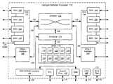
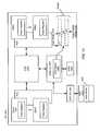
- FIG. 3is an illustration of an INP 310 implemented according to embodiments of the present invention.
- INP 310may be composed of a single silicon integrated circuit die, which may be packaged inside a ceramic, metal, or plastic housing to form a unitary component.
- NP 310includes a BCM 312 which is controlled by a flow identification and scheduler module 314 through a bus 328 .
- the BCM 312may be a multi-ported shared Random Access Memory (RAM) having memory locations mapped as passages, and operating at 224 Gbps.
- the scheduler 314operates under the control of the APEX 316 acting through the bus 330 , and maps the passages of crossbar locations inside the BCM 312 .
- the scheduler 314pre-processes received frames, packets, and PCIe requests before they are acted upon by APEX 316 .
- the scheduler 314also parses received FC frames into correct sequence, and parses received GbE packets (in Internet Protocol (IP) format) into a Transport Control Protocol (TCP) flow.
- IPInternet Protocol
- TCPTransport Control Protocol
- the APEX 316preferably contains five core processors for executing firmware, denoted as processors 318 , 320 , 322 , 324 , and 326 .
- the processors 318 , 322 , 324 , and 326may be core model ARC750 as provided by ARC, Inc., which preferably each have the capability of executing 32 bit Reduced Instruction Set Computer (RISC) firmware with a clock speed of 500 MHz, and may each include 32 KB of dedicated instruction memory (not shown).
- RISCReduced Instruction Set Computer
- the BCM 312is connected to PCS modules 332 and 334 through buses 336 and 338 , respectively.
- PCS module 332is connected to and controls the operation of Combined Media Access Controller (CMAC) modules 340 , 342 , 344 , and 346 .
- the CMAC modules 340 , 342 , 344 , and 346are identical hardware interfaces capable of each communicating using the FC protocol at 1 Gbps, 2 Gbps, and 4 Gbps speeds; and are each capable of communicating using the Ethernet protocol (the Internet Protocol) at 1 Gbps speed (1 GbE).
- the speed and protocol settings for the CMAC modules 340 , 342 , 344 , and 346are controlled by the PCS 332 , which operates in response to control signals from a bus (not shown) connecting the PCS 332 to the APEX 316 .
- the PCS 332also has trunking modes in which it coordinates the operation of the four CMAC modules 340 , 342 , 344 , and 346 together as a single trunk, when such trunking modes are determined by control signals from the APEX 316 .
- One of the trunking modes of the PCS 332causes the CMAC modules 340 , 342 , 344 , and 346 to operate together as a single trunk for 10 Gbps FC protocol (10 Gb FC) provided in an X Attachment Unit Interface (XAUI) trunk as specified by existing FC standards for signaling.
- Another of the trunking modes of the PCS 332causes the CMAC modules 340 , 342 , 344 , and 346 to operate together as a single trunk for 10 Gbps Ethernet protocol (10 GbE) as specified in proposed GbE standards for signaling.
- the PCS 334is connected to the CMAC modules 348 , 350 , 352 , and 354 in the same way that PCS 332 is connected to the CMAC modules 340 , 342 , 344 , and 346 .
- the construction of the PCS 334is preferably the same as the construction of the PCS 332 , but operating independently of the PCS 332 .
- the CMAC modules 348 , 350 , 352 , and 354preferably have the same construction as the CMAC modules 340 , 342 , 344 , and 346 .
- the Root Complex and EndPoint (RC/EP) module 356is connected to the BCM 312 through bus 358 , and is connected to bus interface 360 through bus 362 .
- the bus interface 360is preferably a SERDES for use with PCIe bus signals.
- the bus interface 360is connected to the PCIe bus 364 provided by a host computer (not shown).
- One function of the RC/EP module 356is to send and receive messages in the format determined by the PCIe industry standard, including configuration inquiry responses, separating messages for lanes, and messages for implementing particular functions.
- the PCIe bus 364may have 8 lanes, operating at 2.5 Gbps.
- Physical interface 366includes combined SERDES coupled to each of the CMACs 340 , 342 , 344 , and 346 .
- the function of the interface 366is to selectively provide, under control of signals coupled from the APEX 316 , electronic signals in the FC protocol, GbE protocol, or trunking protocols such as XAUI for 10 Gb FC or 10 GbE.
- the interfaceprovides such electronic signals on port interface connections 368 , 370 , 372 , and 374 which exit the INP 310 .
- the outputsare coupled to transceivers (not shown) which may be optical transceivers for connection to fiber optic cables, or electrical transceivers for connection to electrical cables.
- the physical interface 376is preferably identical in construction to the interface 366 , is coupled to the CMACs 348 , 350 , 352 , and 354 , and has port interface connections 378 , 380 , 382 , and 384 .
- the DMA engine and stream processor 386is connected to the BCM 312 through bus 388 , and is connected to the DDR SDRAM controller 390 through bus 392 .
- the function of the controller 390is to control the sending and receiving of data to and from an external DDR memory module (not shown) connected to the bus 394 of the controller 390 .
- the controller 390includes capabilities for providing RMW, statistics collection, XOR masking for data being transferred to or from the external DDR memory module.
- the data pathway through the bus 392 to the DMA engine and stream processor 386 and through the bus 388 to the BCM 312allows DMA memory operations to occur directly with the controller 390 and its attached DDR memory module, without data flow through the APEX 316 , for data being exchanged with other sources including the PCIe capabilities accessed through the bus 358 and RC/EP module 356 , and the FC and GbE capabilities accessed through the buses 336 and 338 with the PCS modules 332 and 334 .
- the ability to allow direct access for DMA operations through the BCM 312 with the DDR SDRAM controller 390saves time that would be otherwise consumed by data being transferred into and out of the APEX 316 .
- the controller 390is also connected to the scheduler 314 through the bus 396 .
- the controller 390creates queues in the external DDR memory for storing data messages, and writes to and reads from such queues.
- the use of such queues, and the direct memory access to the crossbar BCM 312(through the buses 388 and 392 , controller 390 , and DMA engine and stream processor 386 ) effectively increases the size of the crossbar BCM 312 , and allows more switching pathways to be created than if the BCM 312 were used without the external DDR memory attached to connection 394 .
- the DMA engine and stream processor 386may also perform several data stream transformations, including but not limited to T10.CAP (the Data Integrity protocol standard), data Cyclic Redundancy Check (CRC)/checksum insertion or checking/removal, marker insertion or removal, and transferring data to/from multiple buffers.
- T10.CAPthe Data Integrity protocol standard
- CRCCyclic Redundancy Check
- a Universal Asynchronous Receiver/Transmitter (UART) module 311is provided which allows external control communications with the INP 310 at rates including 10 Megabits per second (Mbps) and 100 Mbps, though a UART connection 313 .
- a support processor 315is connected to exchange messages with the UART module 311 , and has an external connection 317 .
- the support processor 315is preferably a core model ARC750 as provided by ARC, Inc.
- JTAG module 319has an external connection 321 , and is used for boundary scan testing of the hardware contained within the INP 310 .
- the serial flash memory 323has an external connection 325 , is preferably a non-volatile reprogrammable memory which may be loaded through the connection 325 , and stores the firmware for operation of the APEX 316 and support processor 315 .
- FIG. 4is an illustration of the firmware and software structures 410 for use with the INP of FIG. 3 , as implemented according to embodiments of the present invention.
- the structures 410serve to provide the computer codes for activating the INP hardware 412 , and for interacting with a host operating system software structure (not shown) such as Linux or Microsoft Windows.
- the hardware 412is preferably the same as the INP of FIG. 3 .
- On-chip firmware 414 and firmware device emulation programs 416may be downloaded into the hardware 412 , and are for execution by the APEX and support processor of FIG. 3 .
- the firmware 414 and programs 416interact with the hardware 412 through connections 418 and 420 , respectively.
- PIM 422is firmware code for execution by the support processor of FIG. 3 , and includes a boot startup and POST module 424 , online and offline diagnostic program module 426 , configuration and device management module 428 , and status and debug log module 430 .
- the PIM 422may be accessed through the connection 432 .
- the connection 432is preferably the same as the connection 317 of FIG. 3 .
- the on-chip firmware 414 and PIM 422may be accessed by an external software operating system through a hardware abstraction layer 434 , or may be directly accessed through a connection 436 .
- the layer 434is a part of a software driver program which also includes an infrastructure services module 438 , a virtualization and basic copy services module 440 , a Storage Area Network (SAN) services module 442 , an advanced copy services module 444 , an Input/Output Storage Virtualization (IOSV) module 446 , and a network services module 474 .
- SANStorage Area Network
- IOSVInput/Output Storage Virtualization
- the software drivers including the layer 434 and modules 438 , 440 , 442 , 444 , 446 and 474are to be executed as a program on an external host computer processor (not shown) under the control of a host operating system software structure (not shown).
- the infrastructure services module 438includes a discovery and initiator driver 448 , a statistics driver 450 , a FC initiator and target driver 452 , and a device management driver 454 .
- the virtualization and basic copy services module 440includes a virtualization services driver 458 and a basic copy services driver 460 .
- the SAN services module 442includes a performance monitoring module 462 and a routing module 464 .
- the advanced copy services module 444includes a wire splitting module 466 and a journaling module 468 .
- the IOSV module 446includes a multi-RC module 470 and a single RC module 472 .
- the network services module 474includes a Transmission Control Protocol (TCP) Offload Engine (TOE) driver 476 , a Network Interface Card (NIC) driver 478 , and an internet Small Computer System Interface (iSCSI) offload driver 480 .
- TCPTransmission Control Protocol
- TOETransmission Control Protocol
- NICNetwork Interface Card
- iSCSIinternet Small Computer System Interface
- the modules 440 , 442 , 444 , 446 and 474interface with the host operating system software structure (not shown) through the connections 474 , 476 , 478 , 480 and 482 , respectively.
- a host 510may be connected to multiple PCI devices (although only two PCIe devices 512 and 520 are shown) through a PCI bus 514 .
- the PCI standardspecifies that configuration space shall be allocated for each PCI device in the form of configuration registers that consume hardware resources.
- each PCI deviceis assigned one or more mutually-exclusive blocks of memory in the host's memory-mapped memory space 516 .
- host 510has been assigned memory space 518
- PCI device 512has been assigned memory space 524 (designated by the letter “m”)
- PCI device 520has been assigned memory space 526 (designated by the letter “n”).
- each PCI devicemay be allocated up to eight BARs 502 in a configuration header 536 , referred to as BAR 0 -BAR 7 in FIG. 5 .
- Each BARcontains the start address 504 of a block of memory space in memory 516 assigned to a function of the PCI device, and the length 506 and type of memory space 508 (memory or I/O) required by the function.
- the start address 504 of the BARenables a memory or I/O address decoder in the PCI device to detect device accesses whose addresses fall within the block of memory space specified by the BAR.
- other configuration registers 538may be allocated for each PCI device and assigned memory space such that once mapped, a host and the PCI device can communicate using that memory space.
- the host 510performs a configuration cycle where the host first discovers what PCI devices exist on the PCI bus 514 , and then configures the configuration registers for those PCI devices.
- a host's configuration softwaresends a discovery request out over the PCI bus 514 , which reads a subset of each PCI device's configuration registers (e.g. vendor IDentification (ID) register 530 and device ID register 532 ) in configuration header 536 to determine the presence of the PCI device and its device type.
- the host 510also accesses other configuration registers 534 in the PCI device to determine how many blocks of memory the PCI device requires.
- IDvendor IDentification
- the hostsends a configuration request to assign memory space to the PCI device by assigning an address to the BARs of that PCI device.
- the length field 506 and the type field 508 of each BARare generally fixed, and only the address field 504 is programmable.
- a new PCI device 522should be connected to the PCI bus (e.g. in a “hot-plug” event)
- the new devicewill provide an indication back to the host 510 , indicating that a new configuration cycle should be commenced to enable the new PCI device 522 to be discovered and configured (in addition to the re-discovery and reconfiguration of all existing PCI devices).
- the PCI deviceis assigned memory space 528 (designated by the letter “o”), and an indication is sent back to the host, indicating that the configuration cycle for the new PCI device has been terminated.
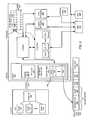
- FIG. 6is an illustration of an exemplary system employing an INP 610 according to embodiments of the present invention.
- INP 610is a simplified representation of the INP of FIG. 3 , emphasizing the PCIe interface.
- FIG. 6illustrates a so-called “single root” system configuration comprised of a single root complex (the host 614 ) and an INP 610 representing one of perhaps several endpoints.
- the hostis logically partitioned into multiple virtual servers, each running a separate “guest” OS 652 .
- the logical partitioning of the host 614is managed by hypervisor software 654 .
- each guest OS 652When each guest OS 652 is initialized, it independently initiates a configuration cycle, allocates itself a certain range of PCI space (e.g. 3 to 4 Gbyte blocks) for each of its BARs, and configures other configuration registers in its configuration header. Because each guest OS 652 operates independently without knowledge of other guest OSs that might be sharing main memory, the address ranges of the BARs of different guest OSs could actually be overlapping.
- the configuration cycle of each guest OS 652is terminated by the hypervisor. However, because the hypervisor 654 manages the configuration space of the guest OSs 652 , inside the hypervisor software is the only place that the guest OSs' configuration space really exists. The hypervisor creates its own configuration space within the INP 610 and manages the system such that the host 614 appears as a single root complex to the INP, and the INP appears to each of the guest OSs in the configuration expected by each guest OS.
- PCI spacee.g. 3 to 4 Gbyte blocks
- a host 614performs a configuration cycle wherein the host first discovers what PCIe devices exist on the PCI bus 612 . To accomplish this, the host's configuration software sends a discovery request out over the PCIe bus 612 , which attempts to read a subset of each PCIe device's configuration registers to determine the presence of the PCIe device and its device type.
- the INP 610is connected to the PCIe bus 612 .
- the INP 610may be configured using firmware to emulate multiple virtual PCIe devices. Any of the processors in the INP 610 , including the APEX 606 (which contains multiple Central Processing Units CPU 0 -CPU 4 ), support processor 626 or the DMA processor 628 , all of which communicate with external DDR memory 630 , may execute firmware to emulate a virtual PCIe device.
- the APEX 606which contains multiple Central Processing Units CPU 0 -CPU 4
- support processor 626 or the DMA processor 628all of which communicate with external DDR memory 630
- the INP 610presents only a single set of eight hardware CSRs (including BARs) 656 within the RC/EP 602 to respond to and terminate the configuration cycle in a manner similar to conventional PCI devices as described above.
- These hardware configuration registersmay be located in a PCIe processing core 650 within the RC/EP 602 .
- the RC/EP 602also includes a virtualization engine 656 which contains logic for virtualizing and configuring the virtual PCIe devices supported by INP 610 .
- the virtualization engine 656is essentially a hardware window through which an entity such as the host 614 can communicate with one or more of the processors in the INP 610 to send and receive messages related to configuration of the virtual PCIe devices, and to send and receive messages related to normal communications (e.g. read and write requests) with the virtual PCIe devices.
- the virtualization engineincludes an aperture or function table (a.k.a. a “classification engine”) 600 containing one aperture or function entry 608 for every BAR in the configuration space of every guest OS 652 (or more generally, for every BAR in the configuration space of one or more OSs communicating with the INP 610 over the PCIe bus 612 ).
- Each aperture table entry 608includes an address field 634 , which includes a base address 636 and a length field 638 that together represent an address range for that entry.
- the entry 608also includes a destination field 640 , which contains the address of the processor (e.g.
- ACLAccess Control List
- the local address field 644stores the address in the INP's memory space (external DDR memory).
- the ACL field 642is a list that allows only certain requestors (guest OSs) to use the particular aperture entry. However, in the present invention all requesters have the same RequesterID, so the ACL field 642 is not utilized.
- Each entry 608also includes a fixed set of rules, wherein each rule can be enabled or disabled by the processor associated with that entry as specified in the destination field 640 .
- the INP 610When the INP 610 is first initialized, its firmware first establishes the configuration space 656 of PCIe core 650 , including the vendor and device type IDs and other configuration registers to be presented to the host 614 , where each configuration register is capable of supporting a different function within the INP. The INP firmware also sets up a default entry 658 in the aperture table. The default entry 658 will redirect all read/write requests to the support processor 626 during the configuration of the virtual PCIe devices.
- a device driver in the hypervisor 654then configures one of the sets of configuration registers in the PCIe core 650 , including the BARs.
- the device driver in the hypervisor 654After the device driver in the hypervisor 654 has discovered and configured the INP 610 as a single PCIe device, the device driver communicates with the INP by sending proprietary CPML messages to the INP, seeking to determine how many virtual PCIe devices the INP supports.
- the CPML messagecontains an address that corresponds to the default entry in the aperture table 600 , so that when the CPML message is received into the INP 610 , it is applied to the aperture table and matched up with the address of the default entry, which then redirects all such CPML requests to the support processor 626 running management software.
- the support processor 626is able to interpret any CPML request received from the device driver in the hypervisor 654 and act accordingly. After the support processor 626 receives the redirected request for the number of supported virtual PCIe devices, the support processor sends a response back to the device driver with an answer.
- the device driver in the hypervisor 654knows the number of guest OSs that have been instantiated, the number of virtual PCIe devices that the INP 610 supports, and that each guest OS expects to see a single PCIe device, the device driver will then send CPML messages to the support processor 626 through the default aperture table entry 658 to create the appropriate number and type of virtual PCIe devices within the INP.
- the virtual PCIe devicesare created by creating a data structure in DDR memory to hold the “state” of a virtual PCIe device (such as the values of its registers, the number of BARs, and the like. (Note that the firmware contains the actual logic to emulate the virtual PCIe devices).
- the device driveralso specifies certain properties of the virtual PCIe devices, such as how many virtual BARs are required, etc. Note that these virtual PCIe devices can be created on demand, so that if a new guest OS is added to the host at a later time, another virtual PCIe device can be created within the INP 610 at that time.
- the support processor 626also configures the aperture table 600 and creates an aperture entry for each BAR associated with each guest OS and corresponding to a newly created virtual PCIe device.
- the device driverwhich knows each of the guest OSs and the address ranges of the BARs for each of the guest OSs, then sends further CPML messages (memory write messages) through the default aperture table entry 658 to the support processor 626 , which configures the corresponding newly created aperture entries so that these addresses point to a processor such as the APEX 606 , where a free processor within the APEX will be responsible for emulating the virtual PCIe device.
- the hypervisor 654is bypassed, and subsequent data transfers occur directly between the drivers in the guest OSs 652 and the INP 610 through read and write commands.
- Read or write requests from a guest OS 652are routed to the aperture table 600 , and logic within the RC/EP module 602 applies the addresses of the requests to the aperture table and compares them with entries representing the BARs for that guest OS to determine if there is an entry having an address range (i.e. a “bin”) encompassing the address of the request. If a match is found, the logic in the RC/EP module 602 performs the action associated with the enabled rules for the matching entry.
- the entrymay result in no further action being taken with regard to the request, or may result in an address translation.
- the entrymay cause the logic to direct the request to one of the processors in APEX 606 via crossbar 610 .
- a free processor in APEX 606then executes the firmware necessary to emulate the performance of the virtual PCIe device associated with that particular entry and respond to the host 614 as though it were a physical PCIe device.
- the firmwaremay be stored in on-chip flash memory or off-chip memory.
- the stored firmware routines executed by a processor in the INP 610are preferably the same as the firmware device emulation programs 416 of FIG. 4 .
- a processor and associated firmwarecan emulate the virtual configuration header 616 of a virtual PCIe device such that all of the fields can be programmable.
- the processor and firmwaremay allocate additional configuration registers 622 and BARs 624 to the virtual PCIe device, up to the limits defined by the PCIe standard.
- An example of the capability of hardware emulation pointed to in the aperture table 600may be firmware that causes the emulation of a FC interface integrated circuit that has been in use for many years (here referred to as a “legacy product”, not shown).
- OSsmay have software drivers which have been fully tested and field proven (here referred to as “legacy drivers”, not shown) for such legacy products.
- the aperture table 600may have an entry denoting such a legacy product, and a corresponding emulation program in the programs 416 , so that when the operating system in the host makes a request through the PCIe bus directed to the legacy product, the INP 610 responds by finding the appropriate entry in the aperture table 600 .
- the APEX 606may then execute the corresponding firmware emulation program in the programs 416 and transfer data messages through the APEX, so that the processor responds over the PCIe bus 612 as if the processor were the legacy product, and the software and firmware structures 410 respond to the legacy driver over the connections 474 , 476 , 478 , 480 , 482 and 436 as if the INP 610 were the legacy product.
- the firmware resident in memory 646e.g. flash memory
- the INP 610provides an indication back to the host 614 , indicating that a new configuration cycle should be commenced to enable the new virtual PCIe device to be discovered and configured, as described above. It should be understood, however, that a new virtual PCIe device of the same class can be supported without having to upgrade the firmware. This is same as when a new guest OS is booted on the host, and the hypervisor wants to create a new virtual device dynamically. In this case, new firmware or a warm reboot is not required.
- each guest OShas a certain number of BARs with certain addresses.
- RBCRequester Control Block
- This data structureis accessible by all of the processors in the APEX 606 , and is used when any of the drivers for one of the guest OSs 652 makes a read or write request.
- OS 1makes a read request to register A in its BAR to read some data from a particular virtual PCIe device
- the aperture table entry for OS 1converts address A to address Y, and the request ends up being processed by the appropriate APEX processor.
- OS 2could have made the same request to read the same data from the same virtual PCIe device, but would have made that request to register K in its BAR. In that case, a different aperture table entry for OS 2 would have translated address K to address Z, and the request would have been processed by the same or a different APEX processor.
- the APEX processorneeds to know which guest OS made the read request.
- the RCBcan be used to make this determination, because the requester database would show that a request with a converted address in the range of A to H (representing a particular aperture table entry) comes from OS 1 , while a request with a converted address in the range of I to O (representing a different particular aperture table entry) comes from OS 2 .
- the datamay be returned (in the case of a read) in a different way.
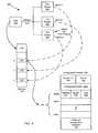
- FIG. 7illustrates an exemplary multi-root system according to embodiments of the present invention.
- the system of FIG. 7includes multiple blades 700 , each with a device driver 704 , and optionally a hypervisor 702 .
- An INP 706as described above, is situated in an I/O blade 708 , which also contains a PCIe switch subsystem 710 .
- the PCIe switch subsystem 710further includes one non-transparent bridge 712 for each blade 700 , and a standard PCIe switch device 714 .
- the PCIe switchis PLX 8532.
- Each non-transparent bridgehas a virtual side and a physical side.
- Each of the blades 700has a PCIe connection 716 to a virtual side of a non-transparent bridge 712 , and the physical side of each non-transparent bridge is connected to the standard PCI switch device 714 .
- the INP 706is connected to the standard PCI switch device via connection 718 .
- both the blades 708 and the INP 706are considered to be root complexes.
- each connection to its corresponding non-transparent bridge 712is like an endpoint, because each blade thinks it is attached to a single PCIe device.
- each blade 700When each blade 700 is powered up and runs through its configuration cycle and discovery process, it independently discovers one device in the form of its corresponding non-transparent bridge 712 , and configures the non-transparent bridge by setting up its configuration space, including the BARs and other configuration registers. The non-transparent bridge then terminates the configuration cycle.
- each non-transparent bridge 712can translate addresses from one domain to another, so in simple terms is an address translation device. This address translation is necessary in the multi-root system of FIG.
- each bladecan talk to its own virtual PCIe device through the one or more aperture entries corresponding to the BARs for the blade, and each blade can operate independently (e.g. perform reads/writes independent of the other blades).
- the way that the INP maintains the requestor information, and how the APEX responds to the requests,is the same as described above for the single-root system.
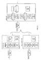
- FIG. 8is an illustration of an exemplary system employing an INP 800 with virtualization logic 826 comprised of programmable configuration logic 802 according to embodiments of the present invention.
- the configuration logic 802may replace the aperture table described above, or may work together with the aperture table. Note that in this alternative embodiment there are no hardware configuration registers in the RC/EP 812 that terminate configuration cycles from the host.
- the configuration logic 802when PCIe transactions 804 are presented to the RC/EP 812 , the headers are evaluated by the configuration logic 802 to determine the classification of the PCIe transaction (i.e. the type of cycle). Depending on the classification, the configuration logic 802 may take no further action with regard to the PCIe transaction, may direct the transaction to a processor via crossbar 810 , or may perform an address translation. For example, if the configuration logic 802 determines that a discovery or configuration request (i.e. a configuration cycle) is being presented, the discovery or configuration request is passed through the crossbar 810 to the APEX 814 .
- a discovery or configuration requesti.e. a configuration cycle
- a free processor in the APEX 814then executes firmware to respond to and terminate the configuration cycle by providing information and indications back to the host indicating that virtual PCIe devices have been discovered and configured.
- the particular processor and firmwareperforms translations from the configuration space of the requestor to the virtual configuration space of the virtual PCIe device being emulated.
- the configuration logicmay be simplified to detect configuration cycles and redirect all configuration cycles to the aperture table, which then makes a further redirection to one of the processors, which responds to and terminates the configuration cycle as discussed above.
- a discovery requestmay be redirected to the APEX 814 through crossbar 810 by aperture table entry 0 representing the BAR for a particular guest OS.
- a free processor in the APEX 814then executes firmware designed to emulate the configuration registers in the configuration header 816 of the particular virtual PCIe device.
- the processorthen provides the contents of an emulated vendor ID register 818 and an emulated device type ID register 820 in response to the discovery request.
- the processoralso provides the contents of other emulated configuration registers 822 to determine how many blocks of memory the particular virtual PCIe device requires.
- the hostthen sends configuration requests that attempt to assign memory space to the virtual PCIe device by assigning addresses to the BARs 824 of that PCIe device.
- these configuration requestsare also redirected to the APEX 814 in accordance with aperture table entry 0 , which receives the addresses and stores them in the emulated BARs 824 of the particular virtual PCIe device.
- embodiments of the present inventioninclude on-chip SERDES 366 and 376 , each SERDES capable of handling multiple (e.g. four) combined GbFC and GbE interfaces (e.g. 1, 2 and 4 GbFC and 1 GbE), one for each CMAC, and capable of being trunked to provide a XAUI.
- multiple CMACscan be configured using support logic to operate in synchronism and cooperation with each other, splitting the signals between them so that a higher speed (e.g. 10 GbFC) can be achieved, with each SERDES effectively running at some intermediate rate (e.g. 3.125 GbFC).
- each CMACis independently programmable and each may be configured to operate at a different speed and a different protocol.
- FIG. 9is an illustration of how the common processing elements of MACs for FC 900 and MACs for GbE 902 can be integrated into an efficient CMAC 904 according to embodiments of the present invention.
- FC framesare received and deserialized by SERDES 906 , and are then processed by a FC MAC 900 .
- This processingtypically includes 32-bit 8b10b decoding 908 , detection of a SFD (a.k.a. a “k” character) and an EFD 910 , CRC 912 , generating packets from the FC frames 914 , and buffering in a FIFO buffer 924 .
- GbE packetsare received and deserialized by SERDES 916 , and are then processed by a GbE MAC 902 .
- This processingtypically includes 8-bit 8b10b decoding 918 , detection of a SFD and an EFD 920 , CRC 922 , and FIFO buffering 926 .
- embodiments of the present inventionintegrate the data paths for both the FC and GbE protocols in a FC/GbE CMAC 904 .
- Both protocolsrequire SERDES 928 , CRC 930 and FIFOs 932 for rate matching, and thus the logic for these tasks is shared in the CMAC 904 .
- the logic (state machine) to perform 8b10b decoding, to detect SFDs and EFDs for each protocol, and to packetize FC framesis different for the two protocols, this logic must be duplicated and switched in or out as needed.
- To produce a FC/GbE CMACmultiple bytes must be framed as packets (even though FC uses “frame” terminology). The bytes in a packet are well-defined in the FC and GbE standards.
- the CMACsare configurable by a processor to decode the incoming packets or frames as either FC “packets” or GbE packets.
- GbE MACshave an address filtering feature.
- address filteringrules can be set in the MAC to not accept certain 16-bit MAC addresses or certain multicast addresses. (With multicast addresses, only a particular group of devices will receive a certain address if a certain bit is set, and each device must be configured to be part of the multicast group. A device could be part of more than one multicast group.)
- Each MACcan be configured to filter packets and to receive only one MAC address (because each MAC has one MAC address assigned to it), and to perhaps receive one or more multicast addresses. Other rules could be set such that the MAC could receive packets only from certain addresses, or that the MAC will not receive from a particular address, but will receive from all other addresses.
- rulescould be used in various combinations. It is up to the device software as to what rules are to be set in each MAC. Conventional MACs support these configurable rules by having configurable registers in hardware, so the rules are limited by limited hardware (e.g. 16 registers would limit the MAC to rules involving not more than 16 addresses).
- FIG. 10illustrates an exemplary INP 1000 employing a hashing scheme for CMAC filtering according to embodiments of the present invention.
- INP 1000 of FIG. 10corresponds to the INP of FIG. 3 , but is simplified to emphasize the hashing scheme.
- the hashing rulesare made scalable without adding hardware, so each CMAC can have many more rules than their hardware registers would allow.
- the scheduler 1002includes a hash engine 1004 . Sophisticated hashing rules can be set for the hash engine 1004 .
- the hash engine 1004can be configured such that for every one of the 2 k destination MAC addresses, a hash entry 1008 is created in off-chip DDR 1010 .
- the DDR 1010can store a large number of hash entries 1008 to achieve scalability.
- the hash entries 1008are created at startup, during configuration, when a host configures the INP 1000 to receive the 2 k destination MAC addresses.
- the scheduler 1002will do a hash of the destination MAC address in the packet, and attempt to match it with one of the hash entries 1008 in DDR 1010 . This is performed by a hardware state machine, so no firmware is required. Although external memory is involved, hardware prefetching is utilized, and thus it may be done at near wire speeds. If a match is found, the packet is then forwarded to one of the APEX processors 1014 .
- a bit in the packetis set indicating a “hash miss.”
- the packetis thereafter still forwarded to the APEX block 1014 , but the APEX firmware will detect the hash miss bit and know that the packet was not to be received, so the packet is discarded.
- the CMAC filteringcan be protocol independent.
- the hashing logic in hash engine 1004knows that the address of a received packet is at a certain offset (e.g. offset 0 ), and the source address is at offset 15 , for example.
- these offsetsare hardwired into the hashing logic, as shown at 1016 .
- the offsetsare programmable, so for example the hashing logic could be configured to look for a field at offset 20 , and read 16 bits from that offset, as shown at 1018 , to accommodate the addressing of any protocol. It is therefore flexible in where it looks for addresses.
- a routing operationcan be described using an example. Referring to FIG. 3 , suppose that CMAC 340 in INP 310 was set to 4GbFC, operating independently, and that CMAC 348 was set to 1 GbE, operating independently. A FC packet is received at CMAC 340 and is routed to the crossbar 312 , which then determines that it should be routed to the APEX 316 .
- the APEX 316When the APEX 316 receives the packet, it determines that the FC packet is supposed to go out of the INP 310 as an Ethernet packet, and thus a conversion from a FC packet to an Ethernet packet (which includes identifying the various fields in the FC packet, removing error correction control bits, and putting the packet back together as an Ethernet packet with the correct addresses and error checking) is performed internal to the INP 310 without communicating with an off-chip host.
- the APEX 316is able to perform this protocol conversion because it was programmed ahead of time by a host to perform a FC to Ethernet packet conversion if a FC packet is received at CMAC 340 with a particular destination address.
- the flow identification/scheduler 314then sends the Ethernet packet out through CMAC 348 corresponding to the destination address of the packet.
- a switching operationcan also be described using an example.
- a FC packetis received at CMAC 342 , and it is routed to the crossbar 312 , which extracts the contents of the packet to determine the destination for the packet.
- the packethas a destination address, and the crossbar 312 must determine the corresponding destination port.
- a lookup tablemay be fetched from off-chip memory that contains preconfigured information that identifies the port number at which the destination address is located. The destination address of the packet is applied to the lookup table to determine the port number to which the packet needs to be forwarded/switched.
- the INP 310operates like a FC switch.
- Previous designshave performed FC to FC switching operations using MACs and a controllable crossbar to determine the destination port based on the contents of the packet, but switching operations combined with the protocol conversion of a routing operation has not previously been performed. Previous designs also did not have a RC/EP module connected directly to the crossbar.
- the INP 310is configurable to perform a switching operation with on-chip FC to Ethernet (and vice versa) conversion without having the data leave the crossbar 312 .
- the headers of the packetmay be modified, but the data is left alone, repacked into a different frame, and shipped out a destination port.
- the conversionis a firmware function with a hardware assist.
- a request for a configuration of a GbE pathway between connections 372 and 368may be provided by a host computer through the PCIe bus 364 .
- the RC/EP 356would respond on the PCIe bus to the host computer, and would utilize its aperture table and/or configuration logic to cause the APEX 316 to activate the scheduler 314 to set the appropriate pathways in the crossbar BCM 312 to move data between CMAC 344 and CMAC 340 , and to cause PCS 322 to cause CMAC 344 , CMAC 340 , and the connections 372 and 368 of interface 344 to use the GbE protocol.
- the host computercould make a request to have a 10 Gbps FC pathway between the connections 378 , 380 , 382 , and 384 in a XAUI arrangement, with the pathway leading to the PCIe bus 364 itself, thus using the INP 310 as a HBA for that configuration.
- the RC/EP 356would further respond by utilizing its aperture table and/or configuration logic to cause the APEX 316 to activate the scheduler 314 to set the appropriate pathways in the crossbar BCM 312 to move data between the PCS 334 and the RC/EP 356 , and to cause PCS 334 to cause CMAC 348 , 350 , 352 , and 354 , and the connections 378 , 380 , 382 , and 384 to use the FC protocol in a XAUI arrangement.
- the RC/EP module 356is connected directly to the crossbar 312 , enabling the RC/EP to function as another packet destination or source.
- PCIeinstead of being able to switch only between SERDES ports, PCIe is now a potential source and destination of the data packets.
- BCMsutilize the concept of credits for their ports. Credits are essentially the number of free buffers at a particular port. For example, if a port on a BCM has eight credits, eight frames of data could be received into that port and stored in the buffers without having to send an acknowledgement. One credit is consumed when a packet is received, and one credit is released when a packet is sent it out of the crossbar through that port. Normally the credits for each of the ports are part of the crossbar, in on-chip memory. However, on-chip memory is expensive, and thus traditionally the number of credits allocated to the ports on a BCM has been limited.
- FIG. 11is an illustration of an INP 1100 employing crossbar credit extensions according to embodiments of the present invention.
- a BCM 1104has multiple ports, each port having a number of credits 1106 for buffering frames as they pass through the BCM 1104 .
- the credit extensions of the present inventionextend the number credits available to each port on the BCM 1104 using off-chip memory 1102 . As a result, on a port by port basis, more credits can be configured than are available in the crossbar memory 1104 .
- the external DDR memory 1102is treated as another port on the crossbar 1104 , or just an extension of the crossbar.
- crossbar logic in the BCM 1104determines that more credits are needed for a particular port, the crossbar logic will make a request to the DMA block 1108 , which has access to the off-chip DDR memory 1102 through the DDR controller 1110 , to effectively gain access to additional credits 1114 .
- the DMA engine 1108treats the off-chip DDR memory 1102 as though it were on-chip memory. When more credits are needed, the off-chip DDR 1102 can be accessed through a port 1112 on the crossbar 1104 and through the DMA engine 1108 to store frames in the DDR 1102 and effectively consume additional credits. Note that this is performed using gates, because the message frames are received so fast that processors would not be able to selectively decide what frames to put in DDR 1102 and which ones to receive from DDR. Instead, the DMA engine 1108 does this work.
Landscapes
- Engineering & Computer Science (AREA)
- Physics & Mathematics (AREA)
- General Engineering & Computer Science (AREA)
- Theoretical Computer Science (AREA)
- Mathematical Physics (AREA)
- Computer Hardware Design (AREA)
- General Physics & Mathematics (AREA)
- Computer Networks & Wireless Communication (AREA)
- Signal Processing (AREA)
- Bus Control (AREA)
Abstract
Description
Claims (75)
Priority Applications (3)
| Application Number | Priority Date | Filing Date | Title |
|---|---|---|---|
| US11/433,728US7743197B2 (en) | 2006-05-11 | 2006-05-11 | System and method for virtualizing PCIe devices |
| US11/707,325US9032164B2 (en) | 2006-02-17 | 2007-02-16 | Apparatus for performing storage virtualization |
| US14/695,272US20150227325A1 (en) | 2006-02-17 | 2015-04-24 | Apparatus for performing storage virtualization |
Applications Claiming Priority (1)
| Application Number | Priority Date | Filing Date | Title |
|---|---|---|---|
| US11/433,728US7743197B2 (en) | 2006-05-11 | 2006-05-11 | System and method for virtualizing PCIe devices |
Publications (2)
| Publication Number | Publication Date |
|---|---|
| US20070266179A1 US20070266179A1 (en) | 2007-11-15 |
| US7743197B2true US7743197B2 (en) | 2010-06-22 |
Family
ID=38686431
Family Applications (1)
| Application Number | Title | Priority Date | Filing Date |
|---|---|---|---|
| US11/433,728Active2028-12-23US7743197B2 (en) | 2006-02-17 | 2006-05-11 | System and method for virtualizing PCIe devices |
Country Status (1)
| Country | Link |
|---|---|
| US (1) | US7743197B2 (en) |
Cited By (56)
| Publication number | Priority date | Publication date | Assignee | Title |
|---|---|---|---|---|
| US20080188832A1 (en)* | 2007-02-06 | 2008-08-07 | Terumo Kabushiki Kaisha | Medical Catheter |
| US20090169020A1 (en)* | 2007-12-28 | 2009-07-02 | Palsamy Sakthikumar | Migration of full-disk encrypted virtualized storage between blade servers |
| US20100180056A1 (en)* | 2009-01-15 | 2010-07-15 | International Business Machines Corporation | Bus access control apparatus and method |
| US20100246594A1 (en)* | 2009-03-31 | 2010-09-30 | Michael Klinglesmith | Flexibly Integrating Endpoint Logic Into Varied Platforms |
| US20110047313A1 (en)* | 2008-10-23 | 2011-02-24 | Joseph Hui | Memory area network for extended computer systems |
| US20110064089A1 (en)* | 2008-05-16 | 2011-03-17 | Youichi Hidaka | Pci express switch, pci express system, and network control method |
| US7979592B1 (en) | 2007-02-09 | 2011-07-12 | Emulex Design And Manufacturing Corporation | Virtualization bridge device |
| US8055807B2 (en)* | 2008-07-31 | 2011-11-08 | International Business Machines Corporation | Transport control channel program chain linking including determining sequence order |
| US8082481B2 (en) | 2008-02-14 | 2011-12-20 | International Business Machines Corporation | Multiple CRC insertion in an output data stream |
| US8095847B2 (en) | 2008-02-14 | 2012-01-10 | International Business Machines Corporation | Exception condition handling at a channel subsystem in an I/O processing system |
| US8108570B2 (en) | 2008-02-14 | 2012-01-31 | International Business Machines Corporation | Determining the state of an I/O operation |
| US8117347B2 (en) | 2008-02-14 | 2012-02-14 | International Business Machines Corporation | Providing indirect data addressing for a control block at a channel subsystem of an I/O processing system |
| US8140713B2 (en) | 2006-10-10 | 2012-03-20 | International Business Machines Corporation | System and program products for facilitating input/output processing by using transport control words to reduce input/output communications |
| US8166206B2 (en) | 2008-02-14 | 2012-04-24 | International Business Machines Corporation | Cancel instruction and command for determining the state of an I/O operation |
| US8176222B2 (en) | 2008-02-14 | 2012-05-08 | International Business Machines Corporation | Early termination of an I/O operation in an I/O processing system |
| US8196149B2 (en) | 2008-02-14 | 2012-06-05 | International Business Machines Corporation | Processing of data to determine compatability in an input/output processing system |
| WO2012023150A3 (en)* | 2010-08-19 | 2012-06-07 | Ineda Systems Pvt. Ltd | Handheld electronic devices |
| US8214562B2 (en) | 2008-02-14 | 2012-07-03 | International Business Machines Corporation | Processing of data to perform system changes in an input/output processing system |
| US8312189B2 (en) | 2008-02-14 | 2012-11-13 | International Business Machines Corporation | Processing of data to monitor input/output operations |
| US8312176B1 (en) | 2011-06-30 | 2012-11-13 | International Business Machines Corporation | Facilitating transport mode input/output operations between a channel subsystem and input/output devices |
| US8332542B2 (en) | 2009-11-12 | 2012-12-11 | International Business Machines Corporation | Communication with input/output system devices |
| US8346978B1 (en) | 2011-06-30 | 2013-01-01 | International Business Machines Corporation | Facilitating transport mode input/output operations between a channel subsystem and input/output devices |
| US8364853B2 (en) | 2011-06-01 | 2013-01-29 | International Business Machines Corporation | Fibre channel input/output data routing system and method |
| US8364854B2 (en) | 2011-06-01 | 2013-01-29 | International Business Machines Corporation | Fibre channel input/output data routing system and method |
| US8392619B2 (en) | 2008-02-14 | 2013-03-05 | International Business Machines Corporation | Providing indirect data addressing in an input/output processing system where the indirect data address list is non-contiguous |
| US8429325B1 (en)* | 2010-08-06 | 2013-04-23 | Integrated Device Technology Inc. | PCI express switch and method for multi-port non-transparent switching |
| US8473641B2 (en) | 2011-06-30 | 2013-06-25 | International Business Machines Corporation | Facilitating transport mode input/output operations between a channel subsystem and input/output devices |
| US8478915B2 (en) | 2008-02-14 | 2013-07-02 | International Business Machines Corporation | Determining extended capability of a channel path |
| US8495253B2 (en) | 2008-02-14 | 2013-07-23 | International Business Machines Corporation | Bi-directional data transfer within a single I/O operation |
| US8549185B2 (en) | 2011-06-30 | 2013-10-01 | International Business Machines Corporation | Facilitating transport mode input/output operations between a channel subsystem and input/output devices |
| US8583989B2 (en) | 2011-06-01 | 2013-11-12 | International Business Machines Corporation | Fibre channel input/output data routing system and method |
| US8677027B2 (en) | 2011-06-01 | 2014-03-18 | International Business Machines Corporation | Fibre channel input/output data routing system and method |
| US8683083B2 (en) | 2011-06-01 | 2014-03-25 | International Business Machines Corporation | Fibre channel input/output data routing system and method |
| US8918542B2 (en) | 2013-03-15 | 2014-12-23 | International Business Machines Corporation | Facilitating transport mode data transfer between a channel subsystem and input/output devices |
| US8976799B1 (en)* | 2007-10-01 | 2015-03-10 | Apple Inc. | Converged computer I/O system and bridging mechanism for peer-to-peer communication |
| US8990439B2 (en) | 2013-05-29 | 2015-03-24 | International Business Machines Corporation | Transport mode data transfer between a channel subsystem and input/output devices |
| US9021155B2 (en) | 2011-06-01 | 2015-04-28 | International Business Machines Corporation | Fibre channel input/output data routing including discarding of data transfer requests in response to error detection |
| US9052837B2 (en) | 2008-02-14 | 2015-06-09 | International Business Machines Corporation | Processing communication data in a ships passing condition |
| US9094287B2 (en) | 2013-06-13 | 2015-07-28 | Cisco Technology, Inc. | System and method for providing a topology path |
| US9112310B2 (en) | 2010-06-30 | 2015-08-18 | Apple Inc. | Spark gap for high-speed cable connectors |
| US9141571B2 (en)* | 2010-12-28 | 2015-09-22 | Avago Technologies General Ip (Singapore) Pte. Ltd. | PCI express switch with logical device capability |
| US9274579B2 (en) | 2010-06-30 | 2016-03-01 | Apple Inc. | Circuitry for active cable |
| US9385478B2 (en) | 2010-06-30 | 2016-07-05 | Apple Inc. | High-speed connector inserts and cables |
| CN105975427A (en)* | 2016-05-18 | 2016-09-28 | 南京国睿中数电子科技有限公司 | PCIE dual-mode system based on SAS interface |
| US9842075B1 (en)* | 2014-09-12 | 2017-12-12 | Amazon Technologies, Inc. | Presenting multiple endpoints from an enhanced PCI express endpoint device |
| US9916273B2 (en) | 2015-07-10 | 2018-03-13 | Microsoft Technology Licensing, Llc | Sideband serial channel for PCI express peripheral devices |
| US9996484B1 (en)* | 2014-09-17 | 2018-06-12 | Amazon Technologies, Inc. | Hardware acceleration for software emulation of PCI express compliant devices |
| US10095534B2 (en) | 2015-02-24 | 2018-10-09 | Red Hat Israel, Ltd. | Guest controlled virtual device packet filtering |
| CN109614359A (en)* | 2018-12-28 | 2019-04-12 | 中科院计算技术研究所南京移动通信与计算创新研究院 | A kind of data transmission method, device and storage medium based on AXI bus |
| US10372650B2 (en) | 2011-02-23 | 2019-08-06 | Apple Inc. | Cross-over and bypass configurations for high-speed data transmission |
| US10452570B1 (en) | 2014-08-27 | 2019-10-22 | Amazon Technologies, Inc. | Presenting physical devices to virtual computers through bus controllers emulated on PCI express endpoints |
| US10860520B2 (en) | 2015-11-18 | 2020-12-08 | Oracle International Corporation | Integration of a virtualized input/output device in a computer system |
| US10871938B2 (en)* | 2013-09-30 | 2020-12-22 | Sonos, Inc. | Playback device using standby mode in a media playback system |
| US11106616B1 (en) | 2019-11-21 | 2021-08-31 | Xilinx, Inc. | Virtualized peripheral component interconnect express (PCIe) device |
| US11256648B1 (en) | 2020-09-29 | 2022-02-22 | Xilinx, Inc. | Virtual hot plug system and method for PCIe devices |
| US20250110908A1 (en)* | 2023-09-29 | 2025-04-03 | Advanced Micro Devices, Inc. | Apparatus and methods for configuring base address registers |
Families Citing this family (215)
| Publication number | Priority date | Publication date | Assignee | Title |
|---|---|---|---|---|
| US7346075B1 (en)* | 2000-02-25 | 2008-03-18 | International Business Machines Corporation | Portable networking interface method and apparatus for distributed switching system |
| US20070217431A1 (en)* | 2005-10-19 | 2007-09-20 | L-3 Communications Titan Corporation | Data security achieved by use of gigabit ethernet and standard ethernet filtering |
| US7694025B1 (en) | 2006-03-31 | 2010-04-06 | Integrated Device Technology, Inc. | Method and device for base address sorting and entry into base address registers |
| US7647438B1 (en)* | 2006-05-09 | 2010-01-12 | Integrated Device Technology, Inc. | Binary base address sorting method and device with shift vector |
| US7779197B1 (en) | 2006-05-09 | 2010-08-17 | Integrated Device Technology, Inc. | Device and method for address matching with post matching limit check and nullification |
| US7725304B1 (en)* | 2006-05-22 | 2010-05-25 | Cadence Design Systems, Inc. | Method and apparatus for coupling data between discrete processor based emulation integrated chips |
| DE102006025133A1 (en)* | 2006-05-30 | 2007-12-06 | Infineon Technologies Ag | Storage and storage communication system |
| US7945721B1 (en)* | 2006-08-11 | 2011-05-17 | Oracle America, Inc. | Flexible control and/or status register configuration |
| US7752376B1 (en)* | 2006-08-11 | 2010-07-06 | Oracle America, Inc. | Flexible configuration space |
| US8683000B1 (en)* | 2006-10-27 | 2014-03-25 | Hewlett-Packard Development Company, L.P. | Virtual network interface system with memory management |
| US7620770B2 (en)* | 2006-11-09 | 2009-11-17 | Ethernity Networks Ltd. | Device and method for storing and processing data units |
| US7836129B2 (en)* | 2006-12-19 | 2010-11-16 | International Business Machines Corporation | Communication between host systems using a queuing system and shared memories |
| US7991839B2 (en)* | 2006-12-19 | 2011-08-02 | International Business Machines Corporation | Communication between host systems using a socket connection and shared memories |
| US8271604B2 (en)* | 2006-12-19 | 2012-09-18 | International Business Machines Corporation | Initializing shared memories for sharing endpoints across a plurality of root complexes |
| US7657663B2 (en) | 2006-12-19 | 2010-02-02 | International Business Machines Corporation | Migrating stateless virtual functions from one virtual plane to another |
| US7984454B2 (en)* | 2006-12-19 | 2011-07-19 | International Business Machines Corporation | Migration of single root stateless virtual functions |
| US7860930B2 (en)* | 2006-12-19 | 2010-12-28 | International Business Machines Corporation | Communication between host systems using a transaction protocol and shared memories |
| US7836238B2 (en)* | 2006-12-19 | 2010-11-16 | International Business Machines Corporation | Hot-plug/remove of a new component in a running PCIe fabric |
| US7813366B2 (en)* | 2006-12-19 | 2010-10-12 | International Business Machines Corporation | Migration of a virtual endpoint from one virtual plane to another |
| US20080192648A1 (en)* | 2007-02-08 | 2008-08-14 | Nuova Systems | Method and system to create a virtual topology |
| JP4839484B2 (en)* | 2007-04-06 | 2011-12-21 | 日本電気株式会社 | Bus connection device, bus connection method, and bus connection program |
| US7752360B2 (en)* | 2007-05-16 | 2010-07-06 | Nuova Systems, Inc. | Method and system to map virtual PCIe I/O devices and resources to a standard I/O bus |
| US9396159B2 (en)* | 2007-09-25 | 2016-07-19 | Oracle America, Inc. | Simple, reliable, connectionless communication mechanism |
| US20090083392A1 (en)* | 2007-09-25 | 2009-03-26 | Sun Microsystems, Inc. | Simple, efficient rdma mechanism |
| US20090198483A1 (en)* | 2008-02-06 | 2009-08-06 | Sezen Uysal | Apparatus and method for network emulation by using hardware accelerated network interface cards |
| US8817656B2 (en)* | 2008-04-08 | 2014-08-26 | Cisco Technology, Inc. | Discovery for fibre channel over ethernet devices |
| FR2932044B1 (en)* | 2008-06-02 | 2010-08-20 | Sagem Comm | METHOD AND DEVICE FOR ALLOCATING MAC ADDRESSES IN A CURRENT COMMUNICATION NETWORK |
| JP2010026726A (en)* | 2008-07-17 | 2010-02-04 | Toshiba Corp | Converter and control system |
| JP2010033125A (en)* | 2008-07-25 | 2010-02-12 | Hitachi Ltd | Storage apparatus and data transfer method |
| KR20100026509A (en)* | 2008-08-29 | 2010-03-10 | 삼성전자주식회사 | Semiconductor device for transmitting a plurality of data flow |
| US9384160B2 (en)* | 2008-09-04 | 2016-07-05 | Avago Technologies General Ip (Singapore) Pte. Ltd. | Methods and controllers for affiliation managment |
| US20100106871A1 (en)* | 2008-10-10 | 2010-04-29 | Daniel David A | Native I/O system architecture virtualization solutions for blade servers |
| US8782746B2 (en) | 2008-10-17 | 2014-07-15 | Comcast Cable Communications, Llc | System and method for supporting multiple identities for a secure identity device |
| EP2698723A1 (en)* | 2010-03-11 | 2014-02-19 | Ricoh Company, Ltd. | Adapter and communication method |
| US8594100B2 (en) | 2010-03-31 | 2013-11-26 | International Business Machines Corporation | Data frame forwarding using a distributed virtual bridge |
| US8619796B2 (en) | 2010-04-22 | 2013-12-31 | International Business Machines Corporation | Forwarding data frames with a distributed fiber channel forwarder |
| US8447909B2 (en)* | 2010-07-19 | 2013-05-21 | International Business Machines Corporation | Register access in distributed virtual bridge environment |
| WO2012023151A2 (en)* | 2010-08-19 | 2012-02-23 | Ineda Systems Pvt. Ltd | I/o virtualization and switching system |
| US8468318B2 (en) | 2010-09-15 | 2013-06-18 | Pure Storage Inc. | Scheduling of I/O writes in a storage environment |
| US11614893B2 (en) | 2010-09-15 | 2023-03-28 | Pure Storage, Inc. | Optimizing storage device access based on latency |
| US8589625B2 (en) | 2010-09-15 | 2013-11-19 | Pure Storage, Inc. | Scheduling of reconstructive I/O read operations in a storage environment |
| US11275509B1 (en) | 2010-09-15 | 2022-03-15 | Pure Storage, Inc. | Intelligently sizing high latency I/O requests in a storage environment |
| US8589655B2 (en) | 2010-09-15 | 2013-11-19 | Pure Storage, Inc. | Scheduling of I/O in an SSD environment |
| US8732426B2 (en) | 2010-09-15 | 2014-05-20 | Pure Storage, Inc. | Scheduling of reactive I/O operations in a storage environment |
| US12008266B2 (en) | 2010-09-15 | 2024-06-11 | Pure Storage, Inc. | Efficient read by reconstruction |
| US9244769B2 (en) | 2010-09-28 | 2016-01-26 | Pure Storage, Inc. | Offset protection data in a RAID array |
| US8775868B2 (en) | 2010-09-28 | 2014-07-08 | Pure Storage, Inc. | Adaptive RAID for an SSD environment |
| US8677176B2 (en) | 2010-12-03 | 2014-03-18 | International Business Machines Corporation | Cable redundancy and failover for multi-lane PCI express IO interconnections |
| US8645746B2 (en) | 2010-12-03 | 2014-02-04 | International Business Machines Corporation | Cable redundancy and failover for multi-lane PCI express IO interconnections |
| JP5706173B2 (en)* | 2011-01-26 | 2015-04-22 | 任天堂株式会社 | Information processing program, information processing apparatus, information processing method, and information processing system |
| CN102694717B (en)* | 2011-03-23 | 2017-04-12 | 华为数字技术(成都)有限公司 | Method, device and system for transmitting messages on PCIE bus |
| US8677024B2 (en)* | 2011-03-31 | 2014-03-18 | International Business Machines Corporation | Aggregating shared Ethernet adapters in a virtualized environment |
| CN102821082A (en)* | 2011-06-10 | 2012-12-12 | 成都市华为赛门铁克科技有限公司 | Data transmission method, device and system |
| US8972611B2 (en)* | 2011-08-11 | 2015-03-03 | Cisco Technology, Inc. | Multi-server consolidated input/output (IO) device |
| US11636031B2 (en) | 2011-08-11 | 2023-04-25 | Pure Storage, Inc. | Optimized inline deduplication |
| US8589640B2 (en) | 2011-10-14 | 2013-11-19 | Pure Storage, Inc. | Method for maintaining multiple fingerprint tables in a deduplicating storage system |
| JP5903801B2 (en)* | 2011-08-23 | 2016-04-13 | 富士通株式会社 | Communication apparatus and ID setting method |
| US8861400B2 (en) | 2012-01-18 | 2014-10-14 | International Business Machines Corporation | Requesting multicast membership information in a distributed switch in response to a miss event |
| US8891535B2 (en) | 2012-01-18 | 2014-11-18 | International Business Machines Corporation | Managing a global forwarding table in a distributed switch |
| US8719540B1 (en) | 2012-03-15 | 2014-05-06 | Pure Storage, Inc. | Fractal layout of data blocks across multiple devices |
| FR2996019B1 (en)* | 2012-09-21 | 2014-10-31 | Thales Sa | CONTROLLER STRUCTURE OF DATA EXCHANGES AND GENERIC AND MULTI-ROLES COMMUNICATIONS |
| US8745415B2 (en) | 2012-09-26 | 2014-06-03 | Pure Storage, Inc. | Multi-drive cooperation to generate an encryption key |
| US10623386B1 (en) | 2012-09-26 | 2020-04-14 | Pure Storage, Inc. | Secret sharing data protection in a storage system |
| US11032259B1 (en) | 2012-09-26 | 2021-06-08 | Pure Storage, Inc. | Data protection in a storage system |
| US11733908B2 (en) | 2013-01-10 | 2023-08-22 | Pure Storage, Inc. | Delaying deletion of a dataset |
| US11768623B2 (en) | 2013-01-10 | 2023-09-26 | Pure Storage, Inc. | Optimizing generalized transfers between storage systems |
| US9063967B2 (en) | 2013-01-10 | 2015-06-23 | Pure Storage, Inc. | Performing copies in a storage system |
| US10908835B1 (en) | 2013-01-10 | 2021-02-02 | Pure Storage, Inc. | Reversing deletion of a virtual machine |
| US9286258B2 (en)* | 2013-06-14 | 2016-03-15 | National Instruments Corporation | Opaque bridge for peripheral component interconnect express bus systems |
| US8943234B1 (en)* | 2013-08-05 | 2015-01-27 | Lsi Corporation | Multi-protocol storage controller |
| US10365858B2 (en) | 2013-11-06 | 2019-07-30 | Pure Storage, Inc. | Thin provisioning in a storage device |
| US10263770B2 (en) | 2013-11-06 | 2019-04-16 | Pure Storage, Inc. | Data protection in a storage system using external secrets |
| US11128448B1 (en) | 2013-11-06 | 2021-09-21 | Pure Storage, Inc. | Quorum-aware secret sharing |
| US9208086B1 (en) | 2014-01-09 | 2015-12-08 | Pure Storage, Inc. | Using frequency domain to prioritize storage of metadata in a cache |
| US9588920B1 (en)* | 2014-02-28 | 2017-03-07 | Qlogic, Corporation | Method and system for port trunking |
| US10656864B2 (en) | 2014-03-20 | 2020-05-19 | Pure Storage, Inc. | Data replication within a flash storage array |
| US9779268B1 (en) | 2014-06-03 | 2017-10-03 | Pure Storage, Inc. | Utilizing a non-repeating identifier to encrypt data |
| US9218244B1 (en) | 2014-06-04 | 2015-12-22 | Pure Storage, Inc. | Rebuilding data across storage nodes |
| US11399063B2 (en) | 2014-06-04 | 2022-07-26 | Pure Storage, Inc. | Network authentication for a storage system |
| US9684575B2 (en)* | 2014-06-23 | 2017-06-20 | Liqid Inc. | Failover handling in modular switched fabric for data storage systems |
| US9218407B1 (en) | 2014-06-25 | 2015-12-22 | Pure Storage, Inc. | Replication and intermediate read-write state for mediums |
| US10496556B1 (en) | 2014-06-25 | 2019-12-03 | Pure Storage, Inc. | Dynamic data protection within a flash storage system |
| US10296469B1 (en) | 2014-07-24 | 2019-05-21 | Pure Storage, Inc. | Access control in a flash storage system |
| US9558069B2 (en) | 2014-08-07 | 2017-01-31 | Pure Storage, Inc. | Failure mapping in a storage array |
| US9495255B2 (en) | 2014-08-07 | 2016-11-15 | Pure Storage, Inc. | Error recovery in a storage cluster |
| US9864761B1 (en) | 2014-08-08 | 2018-01-09 | Pure Storage, Inc. | Read optimization operations in a storage system |
| US10430079B2 (en) | 2014-09-08 | 2019-10-01 | Pure Storage, Inc. | Adjusting storage capacity in a computing system |
| US12175076B2 (en) | 2014-09-08 | 2024-12-24 | Pure Storage, Inc. | Projecting capacity utilization for snapshots |
| US10164841B2 (en) | 2014-10-02 | 2018-12-25 | Pure Storage, Inc. | Cloud assist for storage systems |
| WO2016057315A1 (en)* | 2014-10-05 | 2016-04-14 | Amazon Technologies, Inc. | Emulated endpoint configuration |
| US9489132B2 (en) | 2014-10-07 | 2016-11-08 | Pure Storage, Inc. | Utilizing unmapped and unknown states in a replicated storage system |
| US10430282B2 (en) | 2014-10-07 | 2019-10-01 | Pure Storage, Inc. | Optimizing replication by distinguishing user and system write activity |
| US9727485B1 (en) | 2014-11-24 | 2017-08-08 | Pure Storage, Inc. | Metadata rewrite and flatten optimization |
| US9773007B1 (en) | 2014-12-01 | 2017-09-26 | Pure Storage, Inc. | Performance improvements in a storage system |
| US9552248B2 (en) | 2014-12-11 | 2017-01-24 | Pure Storage, Inc. | Cloud alert to replica |
| US9588842B1 (en) | 2014-12-11 | 2017-03-07 | Pure Storage, Inc. | Drive rebuild |
| US9864769B2 (en) | 2014-12-12 | 2018-01-09 | Pure Storage, Inc. | Storing data utilizing repeating pattern detection |
| US9747245B2 (en)* | 2014-12-17 | 2017-08-29 | Intel Corporation | Method, apparatus and system for integrating devices in a root complex |
| US10545987B2 (en) | 2014-12-19 | 2020-01-28 | Pure Storage, Inc. | Replication to the cloud |
| US11947968B2 (en) | 2015-01-21 | 2024-04-02 | Pure Storage, Inc. | Efficient use of zone in a storage device |
| US10296354B1 (en) | 2015-01-21 | 2019-05-21 | Pure Storage, Inc. | Optimized boot operations within a flash storage array |
| US9710165B1 (en) | 2015-02-18 | 2017-07-18 | Pure Storage, Inc. | Identifying volume candidates for space reclamation |
| US10082985B2 (en) | 2015-03-27 | 2018-09-25 | Pure Storage, Inc. | Data striping across storage nodes that are assigned to multiple logical arrays |
| US10178169B2 (en) | 2015-04-09 | 2019-01-08 | Pure Storage, Inc. | Point to point based backend communication layer for storage processing |
| US10140149B1 (en) | 2015-05-19 | 2018-11-27 | Pure Storage, Inc. | Transactional commits with hardware assists in remote memory |
| US9811483B2 (en)* | 2015-06-19 | 2017-11-07 | Texas Instruments Incorporated | Configurable serial communication hub |
| US9547441B1 (en) | 2015-06-23 | 2017-01-17 | Pure Storage, Inc. | Exposing a geometry of a storage device |
| US10310740B2 (en) | 2015-06-23 | 2019-06-04 | Pure Storage, Inc. | Aligning memory access operations to a geometry of a storage device |
| KR20170028825A (en) | 2015-09-04 | 2017-03-14 | 퓨어 스토리지, 아이앤씨. | Memory-efficient storage and searching in hash tables using compressed indexes |
| US11341136B2 (en) | 2015-09-04 | 2022-05-24 | Pure Storage, Inc. | Dynamically resizable structures for approximate membership queries |
| US11269884B2 (en) | 2015-09-04 | 2022-03-08 | Pure Storage, Inc. | Dynamically resizable structures for approximate membership queries |
| US10623341B2 (en)* | 2015-09-30 | 2020-04-14 | International Business Machines Corporation | Configuration of a set of queues for multi-protocol operations in a target driver |
| US9843453B2 (en) | 2015-10-23 | 2017-12-12 | Pure Storage, Inc. | Authorizing I/O commands with I/O tokens |
| US10452297B1 (en) | 2016-05-02 | 2019-10-22 | Pure Storage, Inc. | Generating and optimizing summary index levels in a deduplication storage system |
| US10133503B1 (en) | 2016-05-02 | 2018-11-20 | Pure Storage, Inc. | Selecting a deduplication process based on a difference between performance metrics |
| US10203903B2 (en) | 2016-07-26 | 2019-02-12 | Pure Storage, Inc. | Geometry based, space aware shelf/writegroup evacuation |
| US10756816B1 (en) | 2016-10-04 | 2020-08-25 | Pure Storage, Inc. | Optimized fibre channel and non-volatile memory express access |
| US10191662B2 (en) | 2016-10-04 | 2019-01-29 | Pure Storage, Inc. | Dynamic allocation of segments in a flash storage system |
| US10162523B2 (en) | 2016-10-04 | 2018-12-25 | Pure Storage, Inc. | Migrating data between volumes using virtual copy operation |
| US10613974B2 (en) | 2016-10-04 | 2020-04-07 | Pure Storage, Inc. | Peer-to-peer non-volatile random-access memory |
| US10481798B2 (en) | 2016-10-28 | 2019-11-19 | Pure Storage, Inc. | Efficient flash management for multiple controllers |
| US10185505B1 (en) | 2016-10-28 | 2019-01-22 | Pure Storage, Inc. | Reading a portion of data to replicate a volume based on sequence numbers |
| US10359942B2 (en) | 2016-10-31 | 2019-07-23 | Pure Storage, Inc. | Deduplication aware scalable content placement |
| US10452290B2 (en) | 2016-12-19 | 2019-10-22 | Pure Storage, Inc. | Block consolidation in a direct-mapped flash storage system |
| US11550481B2 (en) | 2016-12-19 | 2023-01-10 | Pure Storage, Inc. | Efficiently writing data in a zoned drive storage system |
| US11093146B2 (en) | 2017-01-12 | 2021-08-17 | Pure Storage, Inc. | Automatic load rebalancing of a write group |
| US10528488B1 (en) | 2017-03-30 | 2020-01-07 | Pure Storage, Inc. | Efficient name coding |
| US11157422B2 (en) | 2017-03-31 | 2021-10-26 | Intel Corporation | Shared memory for intelligent network interface cards |
| US12045487B2 (en) | 2017-04-21 | 2024-07-23 | Pure Storage, Inc. | Preserving data deduplication in a multi-tenant storage system |
| US11403019B2 (en) | 2017-04-21 | 2022-08-02 | Pure Storage, Inc. | Deduplication-aware per-tenant encryption |
| US10944671B2 (en) | 2017-04-27 | 2021-03-09 | Pure Storage, Inc. | Efficient data forwarding in a networked device |
| US20190004818A1 (en)* | 2017-06-29 | 2019-01-03 | American Megatrends Inc. | Method of UEFI Shell for Supporting Power Saving Mode and Computer System thereof |
| US10402266B1 (en) | 2017-07-31 | 2019-09-03 | Pure Storage, Inc. | Redundant array of independent disks in a direct-mapped flash storage system |
| US10831935B2 (en) | 2017-08-31 | 2020-11-10 | Pure Storage, Inc. | Encryption management with host-side data reduction |
| US10474611B2 (en)* | 2017-09-19 | 2019-11-12 | International Business Machines Corporation | Aligning received bad data indicators (BDIS) with received data on a cross-chip link |
| US10776202B1 (en) | 2017-09-22 | 2020-09-15 | Pure Storage, Inc. | Drive, blade, or data shard decommission via RAID geometry shrinkage |
| US10789211B1 (en) | 2017-10-04 | 2020-09-29 | Pure Storage, Inc. | Feature-based deduplication |
| US10884919B2 (en) | 2017-10-31 | 2021-01-05 | Pure Storage, Inc. | Memory management in a storage system |
| US10860475B1 (en) | 2017-11-17 | 2020-12-08 | Pure Storage, Inc. | Hybrid flash translation layer |
| US10929031B2 (en) | 2017-12-21 | 2021-02-23 | Pure Storage, Inc. | Maximizing data reduction in a partially encrypted volume |
| US11010233B1 (en) | 2018-01-18 | 2021-05-18 | Pure Storage, Inc | Hardware-based system monitoring |
| US11144638B1 (en) | 2018-01-18 | 2021-10-12 | Pure Storage, Inc. | Method for storage system detection and alerting on potential malicious action |
| US10970395B1 (en) | 2018-01-18 | 2021-04-06 | Pure Storage, Inc | Security threat monitoring for a storage system |
| US10467527B1 (en) | 2018-01-31 | 2019-11-05 | Pure Storage, Inc. | Method and apparatus for artificial intelligence acceleration |
| US11036596B1 (en) | 2018-02-18 | 2021-06-15 | Pure Storage, Inc. | System for delaying acknowledgements on open NAND locations until durability has been confirmed |
| US11494109B1 (en) | 2018-02-22 | 2022-11-08 | Pure Storage, Inc. | Erase block trimming for heterogenous flash memory storage devices |
| KR102536637B1 (en)* | 2018-03-29 | 2023-05-26 | 에스케이하이닉스 주식회사 | Memory controller and operating method thereof |
| US11934322B1 (en) | 2018-04-05 | 2024-03-19 | Pure Storage, Inc. | Multiple encryption keys on storage drives |
| US11995336B2 (en) | 2018-04-25 | 2024-05-28 | Pure Storage, Inc. | Bucket views |
| US10678433B1 (en) | 2018-04-27 | 2020-06-09 | Pure Storage, Inc. | Resource-preserving system upgrade |
| US11385792B2 (en) | 2018-04-27 | 2022-07-12 | Pure Storage, Inc. | High availability controller pair transitioning |
| US10678436B1 (en) | 2018-05-29 | 2020-06-09 | Pure Storage, Inc. | Using a PID controller to opportunistically compress more data during garbage collection |
| US11436023B2 (en) | 2018-05-31 | 2022-09-06 | Pure Storage, Inc. | Mechanism for updating host file system and flash translation layer based on underlying NAND technology |
| US10776046B1 (en) | 2018-06-08 | 2020-09-15 | Pure Storage, Inc. | Optimized non-uniform memory access |
| US11281577B1 (en) | 2018-06-19 | 2022-03-22 | Pure Storage, Inc. | Garbage collection tuning for low drive wear |
| US11869586B2 (en) | 2018-07-11 | 2024-01-09 | Pure Storage, Inc. | Increased data protection by recovering data from partially-failed solid-state devices |
| US11133076B2 (en) | 2018-09-06 | 2021-09-28 | Pure Storage, Inc. | Efficient relocation of data between storage devices of a storage system |
| US11194759B2 (en) | 2018-09-06 | 2021-12-07 | Pure Storage, Inc. | Optimizing local data relocation operations of a storage device of a storage system |
| WO2020057638A1 (en)* | 2018-09-21 | 2020-03-26 | Suzhou Kuhan Information Technologies Co., Ltd. | Systems, methods and apparatus for storage controller with multi-mode pcie functionality |
| US10846216B2 (en) | 2018-10-25 | 2020-11-24 | Pure Storage, Inc. | Scalable garbage collection |
| US11113409B2 (en) | 2018-10-26 | 2021-09-07 | Pure Storage, Inc. | Efficient rekey in a transparent decrypting storage array |
| JP6700564B1 (en)* | 2018-12-28 | 2020-05-27 | 富士通クライアントコンピューティング株式会社 | Information processing system |
| US11194473B1 (en) | 2019-01-23 | 2021-12-07 | Pure Storage, Inc. | Programming frequently read data to low latency portions of a solid-state storage array |
| US11588633B1 (en) | 2019-03-15 | 2023-02-21 | Pure Storage, Inc. | Decommissioning keys in a decryption storage system |
| US11334254B2 (en) | 2019-03-29 | 2022-05-17 | Pure Storage, Inc. | Reliability based flash page sizing |
| US11775189B2 (en) | 2019-04-03 | 2023-10-03 | Pure Storage, Inc. | Segment level heterogeneity |
| US11397674B1 (en) | 2019-04-03 | 2022-07-26 | Pure Storage, Inc. | Optimizing garbage collection across heterogeneous flash devices |
| US10990480B1 (en) | 2019-04-05 | 2021-04-27 | Pure Storage, Inc. | Performance of RAID rebuild operations by a storage group controller of a storage system |
| US12087382B2 (en) | 2019-04-11 | 2024-09-10 | Pure Storage, Inc. | Adaptive threshold for bad flash memory blocks |
| US11099986B2 (en) | 2019-04-12 | 2021-08-24 | Pure Storage, Inc. | Efficient transfer of memory contents |
| US11487665B2 (en) | 2019-06-05 | 2022-11-01 | Pure Storage, Inc. | Tiered caching of data in a storage system |
| US11281394B2 (en) | 2019-06-24 | 2022-03-22 | Pure Storage, Inc. | Replication across partitioning schemes in a distributed storage system |
| US10929046B2 (en) | 2019-07-09 | 2021-02-23 | Pure Storage, Inc. | Identifying and relocating hot data to a cache determined with read velocity based on a threshold stored at a storage device |
| US12135888B2 (en) | 2019-07-10 | 2024-11-05 | Pure Storage, Inc. | Intelligent grouping of data based on expected lifespan |
| US11422751B2 (en) | 2019-07-18 | 2022-08-23 | Pure Storage, Inc. | Creating a virtual storage system |
| US11086713B1 (en) | 2019-07-23 | 2021-08-10 | Pure Storage, Inc. | Optimized end-to-end integrity storage system |
| US11963321B2 (en) | 2019-09-11 | 2024-04-16 | Pure Storage, Inc. | Low profile latching mechanism |
| US11403043B2 (en) | 2019-10-15 | 2022-08-02 | Pure Storage, Inc. | Efficient data compression by grouping similar data within a data segment |
| WO2021076333A1 (en)* | 2019-10-15 | 2021-04-22 | Vulcan Technologies Shanghai Co., Ltd. | Intelligent controller and sensor network bus, system and method including smart compliant actuator module |
| US12067118B2 (en) | 2019-11-22 | 2024-08-20 | Pure Storage, Inc. | Detection of writing to a non-header portion of a file as an indicator of a possible ransomware attack against a storage system |
| US11625481B2 (en) | 2019-11-22 | 2023-04-11 | Pure Storage, Inc. | Selective throttling of operations potentially related to a security threat to a storage system |
| US12204657B2 (en) | 2019-11-22 | 2025-01-21 | Pure Storage, Inc. | Similar block detection-based detection of a ransomware attack |
| US11341236B2 (en) | 2019-11-22 | 2022-05-24 | Pure Storage, Inc. | Traffic-based detection of a security threat to a storage system |
| US12050689B2 (en) | 2019-11-22 | 2024-07-30 | Pure Storage, Inc. | Host anomaly-based generation of snapshots |
| US11720692B2 (en) | 2019-11-22 | 2023-08-08 | Pure Storage, Inc. | Hardware token based management of recovery datasets for a storage system |
| US12248566B2 (en) | 2019-11-22 | 2025-03-11 | Pure Storage, Inc. | Snapshot deletion pattern-based determination of ransomware attack against data maintained by a storage system |
| US11657155B2 (en) | 2019-11-22 | 2023-05-23 | Pure Storage, Inc | Snapshot delta metric based determination of a possible ransomware attack against data maintained by a storage system |
| US12079356B2 (en) | 2019-11-22 | 2024-09-03 | Pure Storage, Inc. | Measurement interval anomaly detection-based generation of snapshots |
| US11615185B2 (en) | 2019-11-22 | 2023-03-28 | Pure Storage, Inc. | Multi-layer security threat detection for a storage system |
| US11645162B2 (en) | 2019-11-22 | 2023-05-09 | Pure Storage, Inc. | Recovery point determination for data restoration in a storage system |
| US11520907B1 (en) | 2019-11-22 | 2022-12-06 | Pure Storage, Inc. | Storage system snapshot retention based on encrypted data |
| US12079502B2 (en) | 2019-11-22 | 2024-09-03 | Pure Storage, Inc. | Storage element attribute-based determination of a data protection policy for use within a storage system |
| US12153670B2 (en) | 2019-11-22 | 2024-11-26 | Pure Storage, Inc. | Host-driven threat detection-based protection of storage elements within a storage system |
| US11500788B2 (en) | 2019-11-22 | 2022-11-15 | Pure Storage, Inc. | Logical address based authorization of operations with respect to a storage system |
| US11651075B2 (en) | 2019-11-22 | 2023-05-16 | Pure Storage, Inc. | Extensible attack monitoring by a storage system |
| US12079333B2 (en) | 2019-11-22 | 2024-09-03 | Pure Storage, Inc. | Independent security threat detection and remediation by storage systems in a synchronous replication arrangement |
| US11755751B2 (en) | 2019-11-22 | 2023-09-12 | Pure Storage, Inc. | Modify access restrictions in response to a possible attack against data stored by a storage system |
| US11720714B2 (en) | 2019-11-22 | 2023-08-08 | Pure Storage, Inc. | Inter-I/O relationship based detection of a security threat to a storage system |
| US11687418B2 (en) | 2019-11-22 | 2023-06-27 | Pure Storage, Inc. | Automatic generation of recovery plans specific to individual storage elements |
| US12050683B2 (en)* | 2019-11-22 | 2024-07-30 | Pure Storage, Inc. | Selective control of a data synchronization setting of a storage system based on a possible ransomware attack against the storage system |
| US12411962B2 (en) | 2019-11-22 | 2025-09-09 | Pure Storage, Inc. | Managed run-time environment-based detection of a ransomware attack |
| US11941116B2 (en) | 2019-11-22 | 2024-03-26 | Pure Storage, Inc. | Ransomware-based data protection parameter modification |
| US11675898B2 (en) | 2019-11-22 | 2023-06-13 | Pure Storage, Inc. | Recovery dataset management for security threat monitoring |
| CN111459864B (en)* | 2020-04-02 | 2021-11-30 | 深圳朗田亩半导体科技有限公司 | Memory device and manufacturing method thereof |
| CN112083969B (en)* | 2020-09-09 | 2024-06-04 | 中国航空工业集团公司雷华电子技术研究所 | FC bus communication-based software online loading method |
| CN114741348B (en)* | 2020-12-24 | 2024-12-27 | 华为技术有限公司 | A conversion device, method and integrated circuit |
| US12034749B2 (en)* | 2021-08-23 | 2024-07-09 | Infineon Technologies Ag | Anamoly detection system for peripheral component interconnect express |
| US12367056B2 (en)* | 2021-09-24 | 2025-07-22 | Red Hat, Inc. | Reliable device assignment for virtual machine based containers |
| CN114024796B (en)* | 2021-11-30 | 2023-02-21 | 新华三半导体技术有限公司 | Data sending method, communication device and electronic equipment |
| US11899593B2 (en)* | 2021-12-21 | 2024-02-13 | Intel Corporation | Method and apparatus for detecting ATS-based DMA attack |
| US12170716B2 (en)* | 2023-02-06 | 2024-12-17 | Dell Products L.P. | Conversion of data packets based on internet protocol version |
| CN116232993B (en)* | 2023-02-24 | 2025-03-25 | 新华三半导体技术有限公司 | A method, device and storage medium for transmitting routing table items |
| US11989156B1 (en)* | 2023-03-06 | 2024-05-21 | Dell Products L.P. | Host device conversion of configuration information to an intermediate format to facilitate database transitions |
| US20250036577A1 (en)* | 2023-07-29 | 2025-01-30 | Nxp Usa, Inc. | System and method to facilitate access by a remote computer to a pcie configuration space |
| CN118509395B (en)* | 2024-07-16 | 2024-11-19 | 中电科申泰信息科技有限公司 | 48-Channel 48-port PCIE 5.0 Switch non-blocking switching device |
Citations (9)
| Publication number | Priority date | Publication date | Assignee | Title |
|---|---|---|---|---|
| US20060195618A1 (en)* | 2005-02-25 | 2006-08-31 | International Business Machines Corporation | Data processing system, method, and computer program product for creation and initialization of a virtual adapter on a physical adapter that supports virtual adapter level virtualization |
| US20060253619A1 (en)* | 2005-04-22 | 2006-11-09 | Ola Torudbakken | Virtualization for device sharing |
| US7287114B2 (en)* | 2005-05-10 | 2007-10-23 | Intel Corporation | Simulating multiple virtual channels in switched fabric networks |
| US7356636B2 (en)* | 2005-04-22 | 2008-04-08 | Sun Microsystems, Inc. | Virtualized PCI switch |
| US20080256284A1 (en)* | 2004-03-19 | 2008-10-16 | Koninklijke Philips Electronics N.V. | Simulation Circuit of Pci Express Endpoint and Downstream Port for a Pci Express Switch |
| US7484029B2 (en)* | 2006-02-09 | 2009-01-27 | International Business Machines Corporation | Method, apparatus, and computer usable program code for migrating virtual adapters from source physical adapters to destination physical adapters |
| US7502884B1 (en)* | 2004-07-22 | 2009-03-10 | Xsigo Systems | Resource virtualization switch |
| US7529860B2 (en)* | 2006-12-19 | 2009-05-05 | International Business Machines Corporation | System and method for configuring an endpoint based on specified valid combinations of functions |
| US7613864B2 (en)* | 2005-04-22 | 2009-11-03 | Sun Microsystems, Inc. | Device sharing |
- 2006
- 2006-05-11USUS11/433,728patent/US7743197B2/enactiveActive
Patent Citations (9)
| Publication number | Priority date | Publication date | Assignee | Title |
|---|---|---|---|---|
| US20080256284A1 (en)* | 2004-03-19 | 2008-10-16 | Koninklijke Philips Electronics N.V. | Simulation Circuit of Pci Express Endpoint and Downstream Port for a Pci Express Switch |
| US7502884B1 (en)* | 2004-07-22 | 2009-03-10 | Xsigo Systems | Resource virtualization switch |
| US20060195618A1 (en)* | 2005-02-25 | 2006-08-31 | International Business Machines Corporation | Data processing system, method, and computer program product for creation and initialization of a virtual adapter on a physical adapter that supports virtual adapter level virtualization |
| US20060253619A1 (en)* | 2005-04-22 | 2006-11-09 | Ola Torudbakken | Virtualization for device sharing |
| US7356636B2 (en)* | 2005-04-22 | 2008-04-08 | Sun Microsystems, Inc. | Virtualized PCI switch |
| US7613864B2 (en)* | 2005-04-22 | 2009-11-03 | Sun Microsystems, Inc. | Device sharing |
| US7287114B2 (en)* | 2005-05-10 | 2007-10-23 | Intel Corporation | Simulating multiple virtual channels in switched fabric networks |
| US7484029B2 (en)* | 2006-02-09 | 2009-01-27 | International Business Machines Corporation | Method, apparatus, and computer usable program code for migrating virtual adapters from source physical adapters to destination physical adapters |
| US7529860B2 (en)* | 2006-12-19 | 2009-05-05 | International Business Machines Corporation | System and method for configuring an endpoint based on specified valid combinations of functions |
Non-Patent Citations (2)
| Title |
|---|
| "AN2004 Athens Storage Processor-Single Chip ISCSI, NAS," Product Brief; Astute Networks, San Diego, CA; 2006, MKT-044 Rev. 2.1 (2 pages). |
| "Pericles, The Intelligent Protocol Processor", Product Brief; Astute Networks, San Diego, CA; 2003, MKT-005 Rev. 3.3 (2 pages). |
Cited By (89)
| Publication number | Priority date | Publication date | Assignee | Title |
|---|---|---|---|---|
| US8140713B2 (en) | 2006-10-10 | 2012-03-20 | International Business Machines Corporation | System and program products for facilitating input/output processing by using transport control words to reduce input/output communications |
| US20080188832A1 (en)* | 2007-02-06 | 2008-08-07 | Terumo Kabushiki Kaisha | Medical Catheter |
| US7979592B1 (en) | 2007-02-09 | 2011-07-12 | Emulex Design And Manufacturing Corporation | Virtualization bridge device |
| US8976799B1 (en)* | 2007-10-01 | 2015-03-10 | Apple Inc. | Converged computer I/O system and bridging mechanism for peer-to-peer communication |
| US20090169020A1 (en)* | 2007-12-28 | 2009-07-02 | Palsamy Sakthikumar | Migration of full-disk encrypted virtualized storage between blade servers |
| US9047468B2 (en)* | 2007-12-28 | 2015-06-02 | Intel Corporation | Migration of full-disk encrypted virtualized storage between blade servers |
| US9330042B2 (en) | 2008-02-14 | 2016-05-03 | International Business Machines Corporation | Determining extended capability of a channel path |
| US9436272B2 (en) | 2008-02-14 | 2016-09-06 | International Business Machines Corporation | Providing indirect data addressing in an input/output processing system where the indirect data address list is non-contiguous |
| US8806069B2 (en) | 2008-02-14 | 2014-08-12 | International Business Machines Corporation | Providing indirect data addressing for a control block at a channel subsystem of an I/O processing system |
| US9483433B2 (en) | 2008-02-14 | 2016-11-01 | International Business Machines Corporation | Processing communication data in a ships passing condition |
| US8516161B2 (en) | 2008-02-14 | 2013-08-20 | International Business Machines Corporation | Providing indirect data addressing for a control block at a channel subsystem of an I/O processing system |
| US8495253B2 (en) | 2008-02-14 | 2013-07-23 | International Business Machines Corporation | Bi-directional data transfer within a single I/O operation |
| US8082481B2 (en) | 2008-02-14 | 2011-12-20 | International Business Machines Corporation | Multiple CRC insertion in an output data stream |
| US8095847B2 (en) | 2008-02-14 | 2012-01-10 | International Business Machines Corporation | Exception condition handling at a channel subsystem in an I/O processing system |
| US8108570B2 (en) | 2008-02-14 | 2012-01-31 | International Business Machines Corporation | Determining the state of an I/O operation |
| US8117347B2 (en) | 2008-02-14 | 2012-02-14 | International Business Machines Corporation | Providing indirect data addressing for a control block at a channel subsystem of an I/O processing system |
| US8478915B2 (en) | 2008-02-14 | 2013-07-02 | International Business Machines Corporation | Determining extended capability of a channel path |
| US8166206B2 (en) | 2008-02-14 | 2012-04-24 | International Business Machines Corporation | Cancel instruction and command for determining the state of an I/O operation |
| US8176222B2 (en) | 2008-02-14 | 2012-05-08 | International Business Machines Corporation | Early termination of an I/O operation in an I/O processing system |
| US8838860B2 (en) | 2008-02-14 | 2014-09-16 | International Business Machines Corporation | Determining extended capability of a channel path |
| US8196149B2 (en) | 2008-02-14 | 2012-06-05 | International Business Machines Corporation | Processing of data to determine compatability in an input/output processing system |
| US8892781B2 (en) | 2008-02-14 | 2014-11-18 | International Business Machines Corporation | Bi-directional data transfer within a single I/O operation |
| US8214562B2 (en) | 2008-02-14 | 2012-07-03 | International Business Machines Corporation | Processing of data to perform system changes in an input/output processing system |
| US8312189B2 (en) | 2008-02-14 | 2012-11-13 | International Business Machines Corporation | Processing of data to monitor input/output operations |
| US8392619B2 (en) | 2008-02-14 | 2013-03-05 | International Business Machines Corporation | Providing indirect data addressing in an input/output processing system where the indirect data address list is non-contiguous |
| US9298379B2 (en) | 2008-02-14 | 2016-03-29 | International Business Machines Corporation | Bi-directional data transfer within a single I/O operation |
| US9052837B2 (en) | 2008-02-14 | 2015-06-09 | International Business Machines Corporation | Processing communication data in a ships passing condition |
| US9043494B2 (en) | 2008-02-14 | 2015-05-26 | International Business Machines Corporation | Providing indirect data addressing in an input/output processing system where the indirect data address list is non-contiguous |
| US8977793B2 (en) | 2008-02-14 | 2015-03-10 | International Business Machines Corporation | Determining extended capability of a channel path |
| US8625615B2 (en)* | 2008-05-16 | 2014-01-07 | Nec Corporation | PCI express switch, PCI express system, and network control method |
| US20110064089A1 (en)* | 2008-05-16 | 2011-03-17 | Youichi Hidaka | Pci express switch, pci express system, and network control method |
| US8055807B2 (en)* | 2008-07-31 | 2011-11-08 | International Business Machines Corporation | Transport control channel program chain linking including determining sequence order |
| US20110047313A1 (en)* | 2008-10-23 | 2011-02-24 | Joseph Hui | Memory area network for extended computer systems |
| US20100180056A1 (en)* | 2009-01-15 | 2010-07-15 | International Business Machines Corporation | Bus access control apparatus and method |
| US8185679B2 (en)* | 2009-01-15 | 2012-05-22 | International Business Machines Corporation | Controlling bus access |
| US8831029B2 (en)* | 2009-03-31 | 2014-09-09 | Intel Corporation | Flexibly integrating endpoint logic into varied platforms |
| US20110131362A1 (en)* | 2009-03-31 | 2011-06-02 | Michael Klinglesmith | Flexibly Integrating Endpoint Logic Into Varied Platforms |
| US7873068B2 (en)* | 2009-03-31 | 2011-01-18 | Intel Corporation | Flexibly integrating endpoint logic into varied platforms |
| US20100246594A1 (en)* | 2009-03-31 | 2010-09-30 | Michael Klinglesmith | Flexibly Integrating Endpoint Logic Into Varied Platforms |
| US8537820B2 (en) | 2009-03-31 | 2013-09-17 | Intel Corporation | Flexibly integrating endpoint logic into varied platforms |
| US8537848B2 (en) | 2009-03-31 | 2013-09-17 | Intel Corporation | Flexibly integrating endpoint logic into varied platforms |
| US20110131456A1 (en)* | 2009-03-31 | 2011-06-02 | Michael Klinglesmith | Flexibly Integrating Endpoint Logic Into Varied Platforms |
| US9122811B2 (en) | 2009-03-31 | 2015-09-01 | Intel Corporation | Flexibly integrating endpoint logic into varied platforms |
| US20110080920A1 (en)* | 2009-03-31 | 2011-04-07 | Michael Klinglesmith | Flexibly Integrating Endpoint Logic Into Varied Platforms |
| US8972615B2 (en) | 2009-11-12 | 2015-03-03 | International Business Machines Corporation | Communication with input/output system devices |
| US8332542B2 (en) | 2009-11-12 | 2012-12-11 | International Business Machines Corporation | Communication with input/output system devices |
| US9112310B2 (en) | 2010-06-30 | 2015-08-18 | Apple Inc. | Spark gap for high-speed cable connectors |
| US9385478B2 (en) | 2010-06-30 | 2016-07-05 | Apple Inc. | High-speed connector inserts and cables |
| US9274579B2 (en) | 2010-06-30 | 2016-03-01 | Apple Inc. | Circuitry for active cable |
| US10199778B2 (en) | 2010-06-30 | 2019-02-05 | Apple Inc. | High-speed connector inserts and cables |
| US9494989B2 (en) | 2010-06-30 | 2016-11-15 | Apple Inc. | Power distribution inside cable |
| US8429325B1 (en)* | 2010-08-06 | 2013-04-23 | Integrated Device Technology Inc. | PCI express switch and method for multi-port non-transparent switching |
| WO2012023150A3 (en)* | 2010-08-19 | 2012-06-07 | Ineda Systems Pvt. Ltd | Handheld electronic devices |
| US9141571B2 (en)* | 2010-12-28 | 2015-09-22 | Avago Technologies General Ip (Singapore) Pte. Ltd. | PCI express switch with logical device capability |
| US10372650B2 (en) | 2011-02-23 | 2019-08-06 | Apple Inc. | Cross-over and bypass configurations for high-speed data transmission |
| US8683083B2 (en) | 2011-06-01 | 2014-03-25 | International Business Machines Corporation | Fibre channel input/output data routing system and method |
| US9021155B2 (en) | 2011-06-01 | 2015-04-28 | International Business Machines Corporation | Fibre channel input/output data routing including discarding of data transfer requests in response to error detection |
| US8364853B2 (en) | 2011-06-01 | 2013-01-29 | International Business Machines Corporation | Fibre channel input/output data routing system and method |
| US8364854B2 (en) | 2011-06-01 | 2013-01-29 | International Business Machines Corporation | Fibre channel input/output data routing system and method |
| US8769253B2 (en) | 2011-06-01 | 2014-07-01 | International Business Machines Corporation | Fibre channel input/output data routing system and method |
| US8738811B2 (en) | 2011-06-01 | 2014-05-27 | International Business Machines Corporation | Fibre channel input/output data routing system and method |
| US8683084B2 (en) | 2011-06-01 | 2014-03-25 | International Business Machines Corporation | Fibre channel input/output data routing system and method |
| US8677027B2 (en) | 2011-06-01 | 2014-03-18 | International Business Machines Corporation | Fibre channel input/output data routing system and method |
| US8583988B2 (en) | 2011-06-01 | 2013-11-12 | International Business Machines Corporation | Fibre channel input/output data routing system and method |
| US8583989B2 (en) | 2011-06-01 | 2013-11-12 | International Business Machines Corporation | Fibre channel input/output data routing system and method |
| US8473641B2 (en) | 2011-06-30 | 2013-06-25 | International Business Machines Corporation | Facilitating transport mode input/output operations between a channel subsystem and input/output devices |
| US8631175B2 (en) | 2011-06-30 | 2014-01-14 | International Business Machines Corporation | Facilitating transport mode input/output operations between a channel subsystem and input/output devices |
| US8312176B1 (en) | 2011-06-30 | 2012-11-13 | International Business Machines Corporation | Facilitating transport mode input/output operations between a channel subsystem and input/output devices |
| US8346978B1 (en) | 2011-06-30 | 2013-01-01 | International Business Machines Corporation | Facilitating transport mode input/output operations between a channel subsystem and input/output devices |
| US8549185B2 (en) | 2011-06-30 | 2013-10-01 | International Business Machines Corporation | Facilitating transport mode input/output operations between a channel subsystem and input/output devices |
| US8918542B2 (en) | 2013-03-15 | 2014-12-23 | International Business Machines Corporation | Facilitating transport mode data transfer between a channel subsystem and input/output devices |
| US8990439B2 (en) | 2013-05-29 | 2015-03-24 | International Business Machines Corporation | Transport mode data transfer between a channel subsystem and input/output devices |
| US9195394B2 (en) | 2013-05-29 | 2015-11-24 | International Business Machines Corporation | Transport mode data transfer between a channel subsystem and input/output devices |
| US9094287B2 (en) | 2013-06-13 | 2015-07-28 | Cisco Technology, Inc. | System and method for providing a topology path |
| US11816390B2 (en) | 2013-09-30 | 2023-11-14 | Sonos, Inc. | Playback device using standby in a media playback system |
| US10871938B2 (en)* | 2013-09-30 | 2020-12-22 | Sonos, Inc. | Playback device using standby mode in a media playback system |
| US10452570B1 (en) | 2014-08-27 | 2019-10-22 | Amazon Technologies, Inc. | Presenting physical devices to virtual computers through bus controllers emulated on PCI express endpoints |
| US10095645B2 (en)* | 2014-09-12 | 2018-10-09 | Amazon Technologies, Inc. | Presenting multiple endpoints from an enhanced PCI express endpoint device |
| US9842075B1 (en)* | 2014-09-12 | 2017-12-12 | Amazon Technologies, Inc. | Presenting multiple endpoints from an enhanced PCI express endpoint device |
| US9996484B1 (en)* | 2014-09-17 | 2018-06-12 | Amazon Technologies, Inc. | Hardware acceleration for software emulation of PCI express compliant devices |
| US10095534B2 (en) | 2015-02-24 | 2018-10-09 | Red Hat Israel, Ltd. | Guest controlled virtual device packet filtering |
| US10678583B2 (en) | 2015-02-24 | 2020-06-09 | Red Hat Israel, Ltd. | Guest controlled virtual device packet filtering |
| US9916273B2 (en) | 2015-07-10 | 2018-03-13 | Microsoft Technology Licensing, Llc | Sideband serial channel for PCI express peripheral devices |
| US10860520B2 (en) | 2015-11-18 | 2020-12-08 | Oracle International Corporation | Integration of a virtualized input/output device in a computer system |
| CN105975427A (en)* | 2016-05-18 | 2016-09-28 | 南京国睿中数电子科技有限公司 | PCIE dual-mode system based on SAS interface |
| CN109614359A (en)* | 2018-12-28 | 2019-04-12 | 中科院计算技术研究所南京移动通信与计算创新研究院 | A kind of data transmission method, device and storage medium based on AXI bus |
| US11106616B1 (en) | 2019-11-21 | 2021-08-31 | Xilinx, Inc. | Virtualized peripheral component interconnect express (PCIe) device |
| US11256648B1 (en) | 2020-09-29 | 2022-02-22 | Xilinx, Inc. | Virtual hot plug system and method for PCIe devices |
| US20250110908A1 (en)* | 2023-09-29 | 2025-04-03 | Advanced Micro Devices, Inc. | Apparatus and methods for configuring base address registers |
Also Published As
| Publication number | Publication date |
|---|---|
| US20070266179A1 (en) | 2007-11-15 |
Similar Documents
| Publication | Publication Date | Title |
|---|---|---|
| US7743197B2 (en) | System and method for virtualizing PCIe devices | |
| EP2722771B1 (en) | Controller integration | |
| US9742671B2 (en) | Switching method | |
| CN102576349B (en) | Communication between the host computer and peripheral resources in an input/output (I/O) virtualized system | |
| US7937447B1 (en) | Communication between computer systems over an input/output (I/O) bus | |
| US7983257B2 (en) | Hardware switch for hypervisors and blade servers | |
| US8489778B2 (en) | Method and apparatus for using a single multi-function adapter with different operating systems | |
| US8176204B2 (en) | System and method for multi-host sharing of a single-host device | |
| US9152597B2 (en) | Unified system area network and switch | |
| US8214531B2 (en) | Network configuration synchronization for hardware accelerated network protocol | |
| US8838867B2 (en) | Software-based virtual PCI system | |
| US20110060859A1 (en) | Host-to-host software-based virtual system | |
| WO2012010497A1 (en) | Register access in distributed virtual bridge environment | |
| US11714776B2 (en) | Enabling a multi-chip daisy chain topology using peripheral component interconnect express (PCIe) | |
| CN115437977A (en) | Cross-bus memory mapping | |
| CA2461156C (en) | Software transparent system and method for peer-to-peer message routing | |
| US11321179B1 (en) | Powering-down or rebooting a device in a system fabric | |
| CN109002414A (en) | A kind of cross-node virtual machine communication method and relevant apparatus | |
| Krishnan | Evaluation of an integrated PCI Express IO expansion and clustering fabric | |
| CN117176832A (en) | Exchange chip and control method |
Legal Events
| Date | Code | Title | Description |
|---|---|---|---|
| AS | Assignment | Owner name:EMULEX COMMUNICATIONS CORPORATION, CALIFORNIA Free format text:ASSIGNMENT OF ASSIGNORS INTEREST;ASSIGNORS:CHAVAN, MUKUND T.;RUPANAGUNTA, SRIRAM;REEL/FRAME:017973/0469 Effective date:20060511 Owner name:EMULEX COMMUNICATIONS CORPORATION,CALIFORNIA Free format text:ASSIGNMENT OF ASSIGNORS INTEREST;ASSIGNORS:CHAVAN, MUKUND T.;RUPANAGUNTA, SRIRAM;REEL/FRAME:017973/0469 Effective date:20060511 | |
| AS | Assignment | Owner name:EMULEX DESIGN & MANUFACTURING CORPORATION, CALIFOR Free format text:ASSIGNMENT OF ASSIGNORS INTEREST;ASSIGNOR:EMULEX CORPORATION;REEL/FRAME:021283/0732 Effective date:20080707 Owner name:EMULEX DESIGN & MANUFACTURING CORPORATION,CALIFORN Free format text:ASSIGNMENT OF ASSIGNORS INTEREST;ASSIGNOR:EMULEX CORPORATION;REEL/FRAME:021283/0732 Effective date:20080707 | |
| STCF | Information on status: patent grant | Free format text:PATENTED CASE | |
| FPAY | Fee payment | Year of fee payment:4 | |
| AS | Assignment | Owner name:EMULEX CORPORATION, CALIFORNIA Free format text:ASSIGNMENT OF ASSIGNORS INTEREST;ASSIGNOR:EMULEX DESIGN AND MANUFACTURING CORPORATION;REEL/FRAME:032087/0842 Effective date:20131205 | |
| AS | Assignment | Owner name:AVAGO TECHNOLOGIES GENERAL IP (SINGAPORE) PTE. LTD Free format text:ASSIGNMENT OF ASSIGNORS INTEREST;ASSIGNOR:EMULEX CORPORATION;REEL/FRAME:036942/0213 Effective date:20150831 | |
| AS | Assignment | Owner name:BANK OF AMERICA, N.A., AS COLLATERAL AGENT, NORTH CAROLINA Free format text:PATENT SECURITY AGREEMENT;ASSIGNOR:AVAGO TECHNOLOGIES GENERAL IP (SINGAPORE) PTE. LTD.;REEL/FRAME:037808/0001 Effective date:20160201 Owner name:BANK OF AMERICA, N.A., AS COLLATERAL AGENT, NORTH Free format text:PATENT SECURITY AGREEMENT;ASSIGNOR:AVAGO TECHNOLOGIES GENERAL IP (SINGAPORE) PTE. LTD.;REEL/FRAME:037808/0001 Effective date:20160201 | |
| AS | Assignment | Owner name:AVAGO TECHNOLOGIES GENERAL IP (SINGAPORE) PTE. LTD., SINGAPORE Free format text:TERMINATION AND RELEASE OF SECURITY INTEREST IN PATENTS;ASSIGNOR:BANK OF AMERICA, N.A., AS COLLATERAL AGENT;REEL/FRAME:041710/0001 Effective date:20170119 Owner name:AVAGO TECHNOLOGIES GENERAL IP (SINGAPORE) PTE. LTD Free format text:TERMINATION AND RELEASE OF SECURITY INTEREST IN PATENTS;ASSIGNOR:BANK OF AMERICA, N.A., AS COLLATERAL AGENT;REEL/FRAME:041710/0001 Effective date:20170119 | |
| MAFP | Maintenance fee payment | Free format text:PAYMENT OF MAINTENANCE FEE, 8TH YEAR, LARGE ENTITY (ORIGINAL EVENT CODE: M1552) Year of fee payment:8 | |
| AS | Assignment | Owner name:AVAGO TECHNOLOGIES INTERNATIONAL SALES PTE. LIMITE Free format text:MERGER;ASSIGNOR:AVAGO TECHNOLOGIES GENERAL IP (SINGAPORE) PTE. LTD.;REEL/FRAME:047422/0464 Effective date:20180509 | |
| AS | Assignment | Owner name:AVAGO TECHNOLOGIES INTERNATIONAL SALES PTE. LIMITE Free format text:CORRECTIVE ASSIGNMENT TO CORRECT THE EXECUTION DATE PREVIOUSLY RECORDED AT REEL: 047422 FRAME: 0464. ASSIGNOR(S) HEREBY CONFIRMS THE MERGER;ASSIGNOR:AVAGO TECHNOLOGIES GENERAL IP (SINGAPORE) PTE. LTD.;REEL/FRAME:048883/0702 Effective date:20180905 | |
| MAFP | Maintenance fee payment | Free format text:PAYMENT OF MAINTENANCE FEE, 12TH YEAR, LARGE ENTITY (ORIGINAL EVENT CODE: M1553); ENTITY STATUS OF PATENT OWNER: LARGE ENTITY Year of fee payment:12 |