US7741636B2 - Programmable resistive RAM and manufacturing method - Google Patents
Programmable resistive RAM and manufacturing methodDownload PDFInfo
- Publication number
- US7741636B2 US7741636B2US11/457,702US45770206AUS7741636B2US 7741636 B2US7741636 B2US 7741636B2US 45770206 AUS45770206 AUS 45770206AUS 7741636 B2US7741636 B2US 7741636B2
- Authority
- US
- United States
- Prior art keywords
- conductive
- dielectric layer
- layer
- programmable resistive
- dielectric
- Prior art date
- Legal status (The legal status is an assumption and is not a legal conclusion. Google has not performed a legal analysis and makes no representation as to the accuracy of the status listed.)
- Active, expires
Links
Images


Classifications
- B—PERFORMING OPERATIONS; TRANSPORTING
- B82—NANOTECHNOLOGY
- B82Y—SPECIFIC USES OR APPLICATIONS OF NANOSTRUCTURES; MEASUREMENT OR ANALYSIS OF NANOSTRUCTURES; MANUFACTURE OR TREATMENT OF NANOSTRUCTURES
- B82Y10/00—Nanotechnology for information processing, storage or transmission, e.g. quantum computing or single electron logic
- H—ELECTRICITY
- H10—SEMICONDUCTOR DEVICES; ELECTRIC SOLID-STATE DEVICES NOT OTHERWISE PROVIDED FOR
- H10B—ELECTRONIC MEMORY DEVICES
- H10B63/00—Resistance change memory devices, e.g. resistive RAM [ReRAM] devices
- H10B63/10—Phase change RAM [PCRAM, PRAM] devices
- H—ELECTRICITY
- H10—SEMICONDUCTOR DEVICES; ELECTRIC SOLID-STATE DEVICES NOT OTHERWISE PROVIDED FOR
- H10B—ELECTRONIC MEMORY DEVICES
- H10B63/00—Resistance change memory devices, e.g. resistive RAM [ReRAM] devices
- H10B63/80—Arrangements comprising multiple bistable or multi-stable switching components of the same type on a plane parallel to the substrate, e.g. cross-point arrays
- H—ELECTRICITY
- H10—SEMICONDUCTOR DEVICES; ELECTRIC SOLID-STATE DEVICES NOT OTHERWISE PROVIDED FOR
- H10K—ORGANIC ELECTRIC SOLID-STATE DEVICES
- H10K19/00—Integrated devices, or assemblies of multiple devices, comprising at least one organic element specially adapted for rectifying, amplifying, oscillating or switching, covered by group H10K10/00
- H10K19/10—Integrated devices, or assemblies of multiple devices, comprising at least one organic element specially adapted for rectifying, amplifying, oscillating or switching, covered by group H10K10/00 comprising field-effect transistors
- H—ELECTRICITY
- H10—SEMICONDUCTOR DEVICES; ELECTRIC SOLID-STATE DEVICES NOT OTHERWISE PROVIDED FOR
- H10N—ELECTRIC SOLID-STATE DEVICES NOT OTHERWISE PROVIDED FOR
- H10N70/00—Solid-state devices having no potential barriers, and specially adapted for rectifying, amplifying, oscillating or switching
- H10N70/011—Manufacture or treatment of multistable switching devices
- H—ELECTRICITY
- H10—SEMICONDUCTOR DEVICES; ELECTRIC SOLID-STATE DEVICES NOT OTHERWISE PROVIDED FOR
- H10N—ELECTRIC SOLID-STATE DEVICES NOT OTHERWISE PROVIDED FOR
- H10N70/00—Solid-state devices having no potential barriers, and specially adapted for rectifying, amplifying, oscillating or switching
- H10N70/20—Multistable switching devices, e.g. memristors
- H10N70/231—Multistable switching devices, e.g. memristors based on solid-state phase change, e.g. between amorphous and crystalline phases, Ovshinsky effect
- H—ELECTRICITY
- H10—SEMICONDUCTOR DEVICES; ELECTRIC SOLID-STATE DEVICES NOT OTHERWISE PROVIDED FOR
- H10N—ELECTRIC SOLID-STATE DEVICES NOT OTHERWISE PROVIDED FOR
- H10N70/00—Solid-state devices having no potential barriers, and specially adapted for rectifying, amplifying, oscillating or switching
- H10N70/801—Constructional details of multistable switching devices
- H10N70/821—Device geometry
- H10N70/823—Device geometry adapted for essentially horizontal current flow, e.g. bridge type devices
- H—ELECTRICITY
- H10—SEMICONDUCTOR DEVICES; ELECTRIC SOLID-STATE DEVICES NOT OTHERWISE PROVIDED FOR
- H10N—ELECTRIC SOLID-STATE DEVICES NOT OTHERWISE PROVIDED FOR
- H10N70/00—Solid-state devices having no potential barriers, and specially adapted for rectifying, amplifying, oscillating or switching
- H10N70/801—Constructional details of multistable switching devices
- H10N70/881—Switching materials
- H10N70/882—Compounds of sulfur, selenium or tellurium, e.g. chalcogenides
- H10N70/8828—Tellurides, e.g. GeSbTe
- H—ELECTRICITY
- H10—SEMICONDUCTOR DEVICES; ELECTRIC SOLID-STATE DEVICES NOT OTHERWISE PROVIDED FOR
- H10N—ELECTRIC SOLID-STATE DEVICES NOT OTHERWISE PROVIDED FOR
- H10N70/00—Solid-state devices having no potential barriers, and specially adapted for rectifying, amplifying, oscillating or switching
- H10N70/801—Constructional details of multistable switching devices
- H10N70/881—Switching materials
- H10N70/883—Oxides or nitrides
- H10N70/8833—Binary metal oxides, e.g. TaOx
- H—ELECTRICITY
- H10—SEMICONDUCTOR DEVICES; ELECTRIC SOLID-STATE DEVICES NOT OTHERWISE PROVIDED FOR
- H10N—ELECTRIC SOLID-STATE DEVICES NOT OTHERWISE PROVIDED FOR
- H10N70/00—Solid-state devices having no potential barriers, and specially adapted for rectifying, amplifying, oscillating or switching
- H10N70/801—Constructional details of multistable switching devices
- H10N70/881—Switching materials
- H10N70/883—Oxides or nitrides
- H10N70/8836—Complex metal oxides, e.g. perovskites, spinels
- H—ELECTRICITY
- H10—SEMICONDUCTOR DEVICES; ELECTRIC SOLID-STATE DEVICES NOT OTHERWISE PROVIDED FOR
- H10K—ORGANIC ELECTRIC SOLID-STATE DEVICES
- H10K10/00—Organic devices specially adapted for rectifying, amplifying, oscillating or switching; Organic capacitors or resistors having potential barriers
- H10K10/50—Bistable switching devices
- H—ELECTRICITY
- H10—SEMICONDUCTOR DEVICES; ELECTRIC SOLID-STATE DEVICES NOT OTHERWISE PROVIDED FOR
- H10K—ORGANIC ELECTRIC SOLID-STATE DEVICES
- H10K19/00—Integrated devices, or assemblies of multiple devices, comprising at least one organic element specially adapted for rectifying, amplifying, oscillating or switching, covered by group H10K10/00
- H10K19/202—Integrated devices comprising a common active layer
- H—ELECTRICITY
- H10—SEMICONDUCTOR DEVICES; ELECTRIC SOLID-STATE DEVICES NOT OTHERWISE PROVIDED FOR
- H10K—ORGANIC ELECTRIC SOLID-STATE DEVICES
- H10K85/00—Organic materials used in the body or electrodes of devices covered by this subclass
- H10K85/20—Carbon compounds, e.g. carbon nanotubes or fullerenes
- H10K85/211—Fullerenes, e.g. C60
- H10K85/215—Fullerenes, e.g. C60 comprising substituents, e.g. PCBM
Definitions
- the inventionrelates to integrated circuit nonvolatile memory.
- the inventionrelates to programmable resistive nonvolatile memory, such as phase change memory.
- Nonvolatile memorystores data without requiring a continuous supply of power.
- nonvolatile memoryis useful in not only integrated circuits with nonvolatile storage as a primary purpose, but also integrated circuits with mission mode circuitry besides just data storage.
- multi-function circuitrythat combines multiple functions in this manner is associated with more complex fabrication. If the multi-function integrated circuit was originally designed only with functions other than storage as its primary functions, the fabrication process must be modified to fabricate the nonvolatile storage. It would be desirable if such modifications could be made while minimizing the changes to the fabrication process of the integrated circuit.
- Embodiments of the technologyinclude a method of forming an integrated circuit with nonvolatile memory cells.
- the stepis performed of forming circuitry accessing particular nonvolatile memory cells, prior to the step of forming programmable resistive elements of the nonvolatile memory cells to conductively connect each of the programmable resistive elements with the conductive rows and the conductive columns. Because of the order of the steps in such embodiments, the programmable resistive elements are not damaged by the processes associated with forming the accessing circuitry.
- forming programmable resistive elementsis a last step of fabrication.
- the circuitry accessing particular nonvolatile memory cellsincludes conductive rows accessing the nonvolatile memory cells by row, and conductive columns accessing the nonvolatile memory cells by column.
- conductive rowsaccessing the nonvolatile memory cells by row
- conductive columnsaccessing the nonvolatile memory cells by column.
- particular programmable resistive elementsare addressed by a combination of a selected columns and selected rows.
- conductive columnsinclude a first layer and a second layer at least partly covering the first layer.
- the first and second layers of conductive columnshave at least one of an etching endpoint signal difference and an etching selectivity difference.
- the conductive columnshave a stairstep profile of the first and second layers. The stairstep profile results in one embodiment from removing material excess to the second layer, forming sidewalls at least partly covering the second layer, and removing the sidewalls and conductive material excess to the first layer. Such sidewalls are up to 200 nm thick.
- the accessing circuitryalso includes all transistors of the conductive rows of the integrated circuit.
- a dielectric layeris formed at least partly between the programmable resistive elements and the conductive columns.
- Some embodimentsinclude the step of forming interlayer dielectric, after forming conductive rows and before forming conductive columns. After the interlayer dielectric, then the step is performed of forming at least a first dielectric layer before forming conductive columns.
- the step of forming conductive columns accessing the nonvolatile memory cells by rowincludes the step of removing material excess to a first layer of conductive columns, until reaching at least the first dielectric layer.
- the first dielectric layer and the second dielectric layerhave at least one of an etching endpoint signal difference and an etching selectivity difference.
- Some embodimentsinclude the step of forming at least a second dielectric layer, which at least partly covers the conductive columns and is at least partly adjacent to the first dielectric layer.
- the second dielectric layerhas a thickness of about 10 nm to 50 ⁇ m.
- the stepis performed of forming at least a third dielectric layer substantially to covering the second dielectric layer.
- the second dielectric layer and the third dielectric layerhave at least one of an etching endpoint signal difference and an etching selectivity difference.
- Various embodimentsrelate to forming the vias and the interlayer contacts in the vias.
- the stepis performed of forming holes through the second dielectric layer and the third dielectric layer until reaching the first dielectric layer, to at least partly expose the conductive columns, and to form interlayer contacts between the conductive rows and the programmable resistive elements.
- Some embodimentsinclude the step of forming conductive lining in the holes to conductively connect the conductive columns and the programmable resistive elements.
- Some embodimentsalso include the step of forming conductive structures in the holes to conductively connect the conductive rows and the programmable resistive elements.
- Some embodimentsalso include the step of forming dielectric lining in the holes to allow conductive connection between the conductive rows and the conductive lining only via the programmable resistive elements.
- the dielectric lininghas a thickness between 5 nm and 100 nm.
- various embodimentsinclude the step of performing chemical mechanical polishing. Some embodiments perform chemical mechanical polishing non-selectively among the second dielectric layer, the third dielectric layer, the conductive lining, the dielectric lining, and the conductive structures. Some embodiments perform chemical mechanical polishing to remove the conductive lining until an elevation of the conductive lining is no higher than an elevation of parts of the third dielectric layer by the conductive lining. Some embodiments perform the step of chemical mechanical polishing on parts of the second dielectric and the third dielectric until said parts no longer cover the conductive columns.
- Embodiments of the technologyalso include an integrated circuit with nonvolatile memory cells formed by a process as described above.
- Embodiments of the technologyalso include an integrated circuit with nonvolatile memory cells.
- the integrated circuitincludes circuitry accessing particular nonvolatile memory cells, including: 1) conductive rows accessing the nonvolatile memory cells by row and 2) conductive columns accessing the nonvolatile memory cells by column.
- the integrated circuitalso includes programmable resistive elements of the nonvolatile memory cells. Each of the programmable resistive elements is conductively connected with the conductive rows and the conductive columns. The programmable resistive elements are positioned vertically above the conductive rows and the conductive columns.
- the programmable resistive elementsinclude at least one of: a chalcogenide, Pr x Ca y MnO 3 , PrSrMnO, ZrO x , TCNQ, and PCBM.
- the circuitryincludes a first dielectric layer covering the conductive rows, such that the conductive columns are above the first dielectric layer; a second dielectric layer at least partly adjacent to the conductive columns and at least partly adjacent to the first dielectric layer; a third dielectric layer at least partly covering the second dielectric layer; and interlayer contacts adjacent to the conductive columns.
- the interlayer contactsinclude conductive lining conductively connecting the conductive columns and the programmable resistive elements; dielectric lining allowing conductive connection between the conductive rows and the conductive lining only via the programmable resistive elements; and conductive structures conductively connecting the conductive rows and the programmable resistive elements.
- the first dielectric layerincludes at least one of: SiO x and material having a dielectric constant lower than 3;
- the second dielectric layerincludes at least one of: SiN x , SiO x N y , and SiO x ;
- the third dielectric layerincludes at least one of: SiO x , material having a dielectric constant lower than 3, SiO x N y , and SiN x ;
- the conductive liningincludes at least one of: TiN, Ti, TiN/Ti bilayer, TaN, W, Al, LiNbO 3 , IrO x , RuO x , YBaCuO, LaCaMnO 3 , Pt, metal-silicide, doped poly-Si; and the dielectric lining includes at least one of: SiO x , SiO x N y , SiN x , SrTiO 3 .
- the circuitryfurther comprises a fourth dielectric layer at least partly between the programmable resistive elements and the conductive columns.
- the fourth dielectric layerincludes at least one of: SiO x , SiO x N y , SiN x , SrTiO 3 , and AlO x .
- the conductive columnsinclude first and second layers of conductive columns, such that a stairstep profile characterizes the first and second layers of conductive columns.
- the first layer of conductive columnsincludes at least one of: TiN, Ti, TiN/Ti bilayer, W/TiN bilayer, AlCu/TiN bilayer, doped poly-Si, and metal-silicide; and the second layer of conductive columns includes at least one of: AlCu, TiN/AlCu bilayer, TiN/Ti/AlCu trilayer, W, metal-silicide, and doped poly-Si.
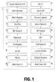
- FIG. 1is an example of a process flow to add programmable resistive memory to an integrated circuit.
- FIG. 2is a cross-sectional view showing the start of photolithography of conductive columns accessing the programmable resistive memory by column.
- FIG. 3is a cross-sectional view showing the sidewall structures on the photoresist covering the conductive columns, to form a stairstep profile between the multiple conductive layers associated with a memory column accessing structure.
- FIG. 4is a cross-sectional view showing the start of photolithography of vias to electrically connect the programmable resistive memory with the conductive rows accessing the programmable resistive memory by row, and to electrically connect the programmable resistive memory with the conductive columns accessing the programmable resistive memory by column.
- FIG. 5is a cross-sectional view showing the sidewall structures in the vias, generated to electrically connect the programmable resistive memory with the conductive columns accessing the programmable resistive memory by column.
- FIG. 6is a cross-sectional view showing the conductive structures in the vias, generated to electrically connect the programmable resistive memory with the conductive rows accessing the programmable resistive memory by row.
- FIG. 7is a cross-sectional view after the removal of excess material by chemical mechanical polishing.
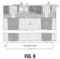
- FIG. 8is a cross-sectional view showing the programmable resistive elements storing nonvolatile data for each nonvolatile memory cell.
- FIG. 9is a top view of an array of programmable resistive nonvolatile memory cells.
- FIG. 10is a cross-sectional view showing the path of current, through the conductive rows accessing the programmable resistive memory by row, the programmable resistive element, and the conductive columns accessing the programmable resistive memory by column.
- FIG. 11is a block diagram of the integrated circuit including an array of nonvolatile programmable resistive memory cells, and other circuitry.
- Various embodimentsare directed at a fast manufacturing method for memory, such as nonvolatile embedded memory implementing resistance device RAM.
- resistance device RAMexamples include resistance memory (RRAM), polymer memory, and phase change memory (PCRAM).
- FIG. 1is an example of a process flow to add programmable resistive memory to an integrated circuit.
- the nonvolatile resistance devicesare designed to be the last process of fabrication.
- the resistive elements of the nonvolatile resistance devicesare just formed on already fabricated electrodes. Before that, no contamination issues arise from resistance device in general fabrication of the remainder of the integrated circuit.
- transistor/row select finish 2the mission circuitry of the integrated circuit other than the programmable resistive nonvolatile storage is fabricated, as well as the row access circuitry of the programmable resistive RAM. After transistor/row select finish 2 , the programmable resistive devices are fabricated. There are only 15 general processing steps 3 prior to the fabrication of the actual programmable resistive elements.
- metal deposition 4metal lithography 6 , and metal etch 8 , the conductive columns accessing the programmable resistive RAM be column are formed. Etching control performed in metal etch 8 forms a stairstep profile out of the conductive columns, lowering contact resistance between the metal line and the programmable resistive element.
- intermetal dielectric deposition 10 and planarization 12Prior to via formation, intermetal dielectric deposition 10 and planarization 12 are performed.
- Via lithography 14 , via etch 16 , and wet dip 18forms the vias for conductive material connecting the row access circuitry to the programmable resistive elements, and for conductive material connecting the column access circuitry to the programmable resistive elements.
- the via holesare self-aligned in the technique of the via etch 16 .
- the stable widths of the insulator and conductor structures in the viasare based on the two etching processes of metal etch 8 and via etch 16 .
- Metal deposition 20 and metal spacer etch 22forms the conductive material connecting the row access circuitry to the programmable resistive elements.
- Dielectric deposition 24 and dielectric etch back 26forms the dielectric which isolates the conductive material connecting the row access circuitry to the programmable resistive elements, from the conductive material connecting the column access circuitry to the programmable resistive elements.
- the electrical performance of the resistive devicesare tunable by changing the thicknesses of the metal and dielectric spacer structures in the vias, formed during metal deposition 20 , metal spacer etch 22 , dielectric deposition 24 , and dielectric etch back 26 .
- Metal deposition 28forms the conductive material connecting the row access circuitry to the programmable resistive elements.
- chemical mechanical polishing 30 and chemical mechanical polishing scrubber 32are performed prior to forming the actual programmable resistive elements.
- the programmable resistive elementsare formed by resistor deposition 34 , resistor lithography 36 , and resistor etch 38 . Finally the fabrication is complete at fabrication out 40 .
- each memory cellfollows or almost follows the horizontal design rule of the transistors.
- the nonvolatile memory cell areais less than 8.5 F 2 with F being the feature size.
- the three self-align processesalso improve yield and form the electrodes prior to the resistive elements.
- the resistance elementsare fabricated last, processes that potentially damage the resistance elements, such as polishing, etching, high temperature treatment, cleaning, etc., are performed prior to forming the resistance elements.
- This processis also a relatively easy way to add embedded memory to an integrated circuit with other mission functions, because foundry processes compatible with conventional semiconductor processing are performed prior to forming the programmable resistive elements.
- the resistive element processingis relatively simplified, requiring only the positioning of the resistive elements on the already formed electrodes.
- FIG. 2is a cross-sectional view showing the start of photolithography of conductive columns accessing the programmable resistive memory by column.
- Dielectric layer 56 , Conductive layer 58 , Conductive layer 60 , and Dielectric layer 62are deposited on a surface of ILD (interlevel-dielectric) 52 , contacts 54 , and LIC (local interconnects, not shown, that are used e.g. for the connection of common source).
- the row select circuitry 50 under the ILD 52 and contacts 54includes circuitry accessing the programmable resistive memory by row such as row select transistors, and circuitry of the integrated circuit other than the programmable resistive nonvolatile storage.
- Example materials of dielectric layer 56are SiO x and low-k material.
- Example materials of conductive layer 58are TiN, Ti, TiN/Ti bilayer, W/TiN bilayer, AlCu/TiN bilayer, doped poly-Si, metal-silicide, etc.
- the material of conductive layer 58has an etching selectivity with respect to conductive layer 60 or an etching endpoint signal difference with conductive layer 60 when etching conductive layer 60 .
- Example materials of conductive layer 60are AlCu, TiN/AlCu bilayer, TiN/Ti/AICu trilayer, W, metal-silicide, doped poly-Si, etc.
- the material of conductive layer 60has good adhesion to conductive layer 58 and etching stops on conductive layer 58 when conductive layer 60 is etched.
- Examples of materials for (conductive layer 60 )/(conductive layer 58 )are: (TiN/Ti/AlCu)/(TiN), (W)/(TiN), (TiN)/(W/TiN), (WSi x )/(n+doped poly-Si), etc.
- Example materials for dielectric layer 62are SiN x , SiO x N y , SiO x , SrTiO 3 , etc.
- the material of dielectric layer 62has good adhesion to the resistive element.
- dielectric layer 62More specific example materials of dielectric layer 62 depend on the material of the resistive element, as follows:
- example materials of dielectric layer 62are SiO x , SiO x N y , and SiN x , due to thermal conductivity concerns.
- example materials of dielectric layer 62are SiO x , SiO x N y , SiN x , and SrTiO 3 , due to adhesion concerns and grown crystal issue.
- example materials of dielectric layer 62are SiO x , SiO x N y , SiN x , and AlO x , due to dielectric constant concern.
- FIG. 2shows the start of photolithography of conductive columns, beginning with the conductive line photoresist 64 .
- the line pitchis the same as that of the transistor contact.
- the conductive line directionis perpendicular to the row access circuitry, such as gates of transistors or LIC of transistors in the row select circuitry 50 .
- FIG. 3is a cross-sectional view showing the sidewall structures on the photoresist covering the conductive columns, to form a stairstep profile between the multiple conductive layers associated with a memory column accessing structure.
- Dielectric layer 62 and conductive layer 60are etched using photoresist 64 and suitable etch chemistries.
- etching dielectric layer 62depend on the material of the dielectric layer 62 , as follows:
- etching examplesare reactive-ion-etching with CF 4 , CHF 3 , Ar, and N 2 , etc. to open dielectric layer 62 .
- etching examplesare reactive-ion-etching with CF 4 , CHF 3 , CH 2 F 2 , CH 3 F, O 2 , and Ar, etc. to open dielectric layer 62 .
- etching examplesare reactive-ion-etching with CF 4 , BCl 3 , NF 3 , CO, O 2 , and Ar, etc. to open dielectric layer 62 .
- Conductive layer 60is etched using suitable chemistries, stopping on conductive layer 58 by etching selectivity or by catching an etching endpoint signal.
- etching conductive layer 60depend on the material of the conductive layer 60 , as follows:
- etching examplesare reactive-ion-etching with Cl 2 , BCl 3 , Ar, and N 2 etc. to open conductive layer 60 , using an etching endpoint signal to stop on conductive layer 58 .
- etching examplesinclude reactive-ion-etching with SF6, O2, N2, and Ar, etc. to open conductive layer 60 , using the high etching selectivity of W to TiN.
- etching examplesinclude reactive-ion-etching with Cl 2 , N 2 , He/O 2 , CF 4 , O 2 , and/or Ar, etc., to open conductive layer 60 , using an endpoint signal to stop on conductive layer 58 .
- Polymer sidewallsare generated, with chemistry examples as follows: C 4 F 8 , C 4 F 6 , C 5 F 8 , CF 4 , CH 3 F, CHF 3 , CH 2 F 2 , Ar, N 2 , and/or O 2 with suitable power, pressure, and other parameters.
- the thickness of the polymer sidewallranges from 10 nm ⁇ 200 nm.
- the polymer sidewallsare etched using reactive-ion-etching that is the same as dielectric layer 62 and conductive layer 60 with suitable chemistries.
- FIG. 4is a cross-sectional view showing the start of photolithography of vias to electrically connect the programmable resistive memory with the conductive rows accessing the programmable resistive memory by row, and to electrically connect the programmable resistive memory with the conductive columns accessing the programmable resistive memory by column.
- Conductive layer 58is etched, stopping on dielectric layer 56 using as a mask the sidewall polymer and the photoresist remaining for metal line lithography.
- etching conductive layer 58depend on the material of the conductive layer 58 , as follows:
- etching examplesinclude reactive-ion-etching with Cl 2 , BCl 3 , Ar, and/or N 2 etc. to open conductive layer 58 , using the high etching selectivity of TiN to SiO 2 .
- etching examplesinclude reactive-ion-etching with HBr, Cl 2 , N 2 , He/O 2 , O 2 , and/or Ar, etc. to open conductive layer 58 , using the high etching selectivity of TiN to SiO 2 .
- the polymer residueis stripped using O 2 , N 2 , and/or N 2 /H 2 plasma.
- the metal linebecomes a self-aligned stairstep shape.
- the step widthdepends on the thickness of the polymer sidewall.
- the dielectric layer 68is deposited on dielectric layer 56 , conductive layer 58 , conductive layer 60 , and dielectric layer 62 .
- the material of dielectric layer 68is SiN x , SiO x N y , SiO x , etc.
- Dielectric layer 68acts as the dry etching stop layer of dielectric layer 70 .
- Dielectric layer 68is selectively wet etched to open the stairstep of conductive layer 58 after the further via etch, so the dielectric layer 68 has wet etching selectivity to dielectric layer 56 .
- the materials of dielectric layer 68 /dielectric layer 56are SiN x /SiO x .
- the thickness of dielectric layer 68can be 10 nm ⁇ 50 mm.
- Dielectric layer 70is deposited on dielectric layer 68 .
- Dielectric layer 70can be SiO x , low-k material, SiO x N y , and/or SiN x , etc.
- the dielectric layer 70is mainly intermetal dielectric (IMD) material.
- Dielectric layer 70can be made by high-density plasma (HDP) CVD, spin-on-glass (SOG), plasma-enhanced CVD (PECVD), and/or spin-coating method with or without chemical-mechanical-polishing (CMP).
- the material of dielectric layer 70is different from that of dielectric layer 68 .
- Example materials of dielectric layer 70 /dielectric layer 68are SiO x /SiN x .
- via hole photolithographyis performed.
- the pitchcan be same as that of contact of transistor and metal line. Part of the exposed via hole overlaps the conductive line 58 / 60 .
- the via-hole photolithography processbegins with the photoresist 72 .
- FIG. 5is a cross-sectional view showing the sidewall structures in the vias, generated to electrically connect the programmable resistive memory with the conductive columns accessing the programmable resistive memory by column.
- Etching of viasis performed, stopping on dielectric layer 68 , using via-hole photoresist. Damage is prevented from the etching of dielectric layer 70 , due to the high etching selectivity to dielectric layer 68 , dielectric layer 56 , conductive layer 58 , conductive layer 60 , and dielectric layer 62 .
- etching dielectric layer 70depend on the material of dielectric layer 70 , as follows:
- etching examplesinclude reactive-ion-etching with C 4 F 8 , C 4 F 6 , CHF 3 , CF 4 , Ar, O 2 , and/or N 2 etc. to open dielectric layer 70 and stop on dielectric layer 68 , using the high etching selectivity of SiO x to SiN x .
- the polymer residueis stripped using O 2 , N 2 , and/or N 2 /H 2 plasma.
- Dielectric layer 68is wet etched using a suitable solvent. The wet dip of dielectric layer 68 opens the conductive layer 58 stairstep and conductive layer 60 , but without opening dielectric layer 56 .
- wet etching dielectric layer 68depend on the materials of dielectric layer 68 , as follows:
- wet etching examplesinclude a tank process with hot phosphoric acid to open dielectric layer 68 and stop on dielectric layer 56 , using the high etching selectivity of SiN x to SiO x .
- Dielectric layer 62can have the same material or a different material from dielectric layer 68 . If the materials are the same, the wet dip time is short to just open dielectric layer 68 .
- the conductive structure 74is deposited on dielectric layer 56 , with good conformality to conductive layer 58 , conductive layer 60 , and dielectric layer 70 .
- the conductive structure 74can be made by CVD, MOCVD, or electrodeposition etc.
- the material of the conductive structure 74is TiN, Ti, TiN/Ti bilayer, TaN, W, Al, LiNbO 3 , IrO x , RuO x , YBaCuO, LaCaMnO 3 , Pt, metal-silicide, doped poly-Si, or etc.
- Specific examples of the conductive structure 74depend on the material of the resistive element, as follows:
- examples of conductive structure 74include TiN, TaN, W, or LiNbO 3 etc.
- examples of conductive structure 74include LiNbO 3 , YBaCuO, LaCaMnO 3 , or Pt etc.
- examples of conductive structure 74include Al or TiN etc.
- the conductive structure 74 etchuses high bombardment reactive-ion plasma, such as Ar, CF4, and/or suitable chemistries, to form a straight conductive structure 74 around the via hole.
- high bombardment reactive-ion plasmasuch as Ar, CF4, and/or suitable chemistries, to form a straight conductive structure 74 around the via hole.
- the polymer residueis stripped using O2, N2, and/or N2/H2 plasma.
- FIG. 6is a cross-sectional view showing the conductive structures in the vias, generated to electrically connect the programmable resistive memory with the conductive rows accessing the programmable resistive memory by row.
- Dielectric structure 76is deposited on dielectric layer 70 , conductive structure 74 and dielectric layer 56 with good conformality.
- Dielectric structure 76can be SiO x , SiO x N y , SiN x , SrTiO 3 , etc.
- the material of dielectric structure 76has good adhesion to the resistive element.
- dielectric structure 76depend on the material of the resistive element, as follows:
- examples of the dielectric structure 76include SiO x , SiO x N y , and SiN x due to thermal conductivity concerns.
- examples of dielectric structure 76include SiO x , SiO x N y , SiN x , or SrTiO 3 due to adhesion concerns and grown crystal issues.
- examples of dielectric structure 76include SiO x , SiO x N y , and SiN x , or AlO x due to dielectric constant concerns.
- Dielectric structure 76is etched without a mask using high bombardment.
- etchingdepend on the material of the dielectric structure 76 and dielectric layer 56 , as follows Etching dielectric structure 76 method examples:
- examples of etchinginclude reactive-ion-etching with CF 4 , CHF 3 , Ar, and/or N 2 etc. to open dielectric structure 76 and dielectric layer 56 , stopping at contact 54 leading to the row select circuitry 50 .
- examples of etchinginclude reactive-ion-etching with CF 4 , BCl 3 , NF 3 , CO, O 2 , and/or Ar, etc. to open dielectric structure 76 and transfer reactive-ion-etching with CF 4 , CHF 3 , Ar, and/or N 2 etc. to open dielectric layer 56 , stopping at contact 54 leading to the row select circuitry 50 .
- the etching rate of conductive structure 74is low during etching dielectric structure 76 and dielectric layer 56 . So conductive structure 74 is exposed.
- Dielectric structure 76prevents conductive structure 74 from current leakage to row select circuitry 50 .
- the thickness of the dielectric structure 76ranges from 5 nm ⁇ 100 nm. (i.e., width of dielectric structure 76 Spacer ranges 5 nm ⁇ 100 nm.)
- the polymer residueis stripped using O2, N2, and/or N2/H2 plasma.
- Conductive electrode 78fills in the hole defined by dielectric structure 76 .
- the conductive electrode 78connects to the contact 54 of the row select circuitry 50 .
- Conductive electrode 78is deposited on dielectric layer 70 , conductive structure 74 , dielectric structure 76 , dielectric layer 56 , and contact 54 of row select circuitry 50 .
- Conductive electrode 78can be CVD W, or CVD TiN, PVD TaN/electrodeposited Cu, etc. with enough thickness to cover the whole surface.
- FIG. 7is a cross-sectional view after the removal of excess material by chemical mechanical polishing.
- CMP of conductive electrode 78plays an important role of yield.
- Conductive electrode 78is polished until conductive structure 74 is exposed, and further polished until touching dielectric layer 70 .
- Dielectric layer 70is polished until dielectric layer 68 is exposed, and further polished until exposing dielectric layer 62 .
- the CMP slurryhas no significant selective polishing rate to dielectric layer 70 , dielectric layer 68 , dielectric structure 76 , conductive electrode 78 , and conductive structure 74 .
- An example of slurryis SiO2.
- the width of dielectric structure 76 and conductive structure 74is uniform for similarly uniform electric performance.
- a scrubber cleaning after polishingensures an open circuit between conductive electrode 78 and conductive structure 74 ,
- FIG. 8is a cross-sectional view showing the programmable resistive elements 80 storing nonvolatile data for each nonvolatile memory cell.
- resistive element depositiondepends on the type of programmable resistive nonvolatile memory device, as follows:
- example materials of resistive elementsinclude Ge x Sb y Te z (GST), N 2 -doped GST, Ge x Sb y , or any kind of material that uses different crystallized phase changes to determine resistance.
- example materials of resistive elementsinclude PrCaMnO 3 , PrSrMnO 3 , ZrO x , or any kind of materials that can use voltage pulse (differently polarized) to change and retain the resistance state.
- example materials of resistive elementsinclude Cu-TCNQ, Ag-TCNQ, C 60 -TCNQ, or any kind of metal doped-TCNQ, PCBM, TCNQ-PCBM, or any kind of polymer material that has bistable or multi-stable resistance states controlled by a voltage pulse or by a current density.
- the resistive elementcan include any kind of material that is 2-terminal controlled and has bistable or multi-stable resistance states, controlled by voltage, current density, current polarization, or any kind of electrical characterization.
- the resistive element 80has a thickness, which depends on the material properties, and is deposited on conductive electrode 78 and conductive structure 74 to conductively connect to both.
- the distance between conductive electrode 78 and conductive structure 74is tunable and depends on the width of the dielectric structure 76 .
- the resistive elementhas a cap layer to prevent changes in characteristics due to air exposure.
- the resistive element patternis defined by a rectangle-shaped photolithography.
- the length dimensionis orthogonal to the direction of the conductive columns formed by conductive layer 60 and conductive layer 58 .
- the length of the resistive elementruns from within an area defined by conductive electrode 78 , over dielectric structure 76 , conductive structure 74 , and ending within an area defined by dielectric layer 62 .
- a trimming or shrinkage processsuch as cap layer wet dip can be used.
- etching chemistry of resistive element etchingdepend on the material of the resistive element, as follows:
- etching chemistry examplesinclude CF 4 , Cl 2 , Ar, O 2 , CHF 3 , BCl 3 , and/or N 2 etc.
- etching chemistry examplesinclude Ar, CF 4 , and/or O 2 etc. to etch with high bombardment.
- etching chemistry examplesinclude O 2 , Ar, and/or CF 4 to etch with cap layer hard-mask.
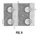
- FIG. 9is a top view of an array of programmable resistive nonvolatile memory cells.
- each contact 54are positioned beneath a corresponding conductive structure 74 , dielectric structure 76 , and conductive electrode 78 , the lateral positions of the contacts 54 are indicated by hyphenated outlines. Shown is an exposed part of dielectric layer 68 , shaped as a stripe parallel to the conductive columns 58 and 60 and the dielectric layer 62 . Also shown is an exposed part of dielectric layer 62 adjacent to the exposed part of dielectric layer 68 , and an exposed part of dielectric layer 70 adjacent to an exposed part of dielectric layer 68 and an exposed part of dielectric layer 62 . As with FIG. 8 , resistive element 80 is shown in conductive connection with conductive electrode 78 and conductive structure 74 .
- Embodiments of the memory cellinclude phase change based memory materials, including chalcogenide based materials and other materials, for the resistive element 80 .
- Chalcogensinclude any of the four elements oxygen (O), sulfur (S), selenium (Se), and tellurium (Te), forming part of group VI of the periodic table.
- Chalcogenidescomprise compounds of a chalcogen with a more electropositive element or radical.
- Chalcogenide alloyscomprise combinations of chalcogenides with other materials such as transition metals.
- a chalcogenide alloyusually contains one or more elements from column six of the periodic table of elements, such as germanium (Ge) and tin (Sn).
- chalcogenide alloysinclude combinations including one or more of antimony (Sb), gallium (Ga), indium (In), and silver (Ag).
- Sbantimony
- Gagallium
- Inindium
- silversilver
- phase change based memory materialsinclude alloys of: Ga/Sb, In/Sb, In/Se, Sb/Te, Ge/Te, Ge/Sb/Te, In/Sb/Te, Ga/Se/Te, Sn/Sb/Te, In/Sb/Ge, Ag/In/Sb/Te, Ge/Sn/Sb/Te, Ge/Sb/Se/Te and Te/Ge/Sb/S.
- compositionscan be workable.
- the compositionscan be characterized as TeaGebSb 100 ⁇ (a+b).
- One researcherhas described the most useful alloys as having an average concentration of Te in the deposited materials well below 70%, typically below about 60% and ranged in general from as low as about 23% up to about 58% Te and most preferably about 48% to 58% Te.
- Concentrations of Gewere above about 5% and ranged from a low of about 8% to about 30% average in the material, remaining generally below 50%. Most preferably, concentrations of Ge ranged from about 8% to about 40%. The remainder of the principal constituent elements in this composition was Sb.
- a transition metalsuch as chromium (Cr), iron (Fe), nickel (Ni), niobium (Nb), palladium (Pd), platinum (Pt) and mixtures or alloys thereof may be combined with Ge/Sb/Te to form a phase change alloy that has programmable resistive properties.
- chromium (Cr)iron (Fe), nickel (Ni), niobium (Nb), palladium (Pd), platinum (Pt) and mixtures or alloys thereof
- Ge/Sb/Techromium
- Specific examples of memory materials that may be usefulare given in Ovshinsky '112 at columns 11-13, which examples are hereby incorporated by reference.
- Phase change alloysare capable of being switched between a first structural state in which the material is in a generally amorphous solid phase, and a second structural state in which the material is in a generally crystalline solid phase in its local order in the active channel region of the cell. These alloys are at least bistable.
- amorphousis used to refer to a relatively less ordered structure, more disordered than a single crystal, which has the detectable characteristics such as higher electrical resistivity than the crystalline phase.
- crystallineis used to refer to a relatively more ordered structure, more ordered than in an amorphous structure, which has detectable characteristics such as lower electrical resistivity than the amorphous phase.
- phase change materialsmay be electrically switched between different detectable states of local order across the spectrum between completely amorphous and completely crystalline states.
- Other material characteristics affected by the change between amorphous and crystalline phasesinclude atomic order, free electron density and activation energy.
- the materialmay be switched either into different solid phases or into mixtures of two or more solid phases, providing a gray scale between completely amorphous and completely crystalline states.
- the electrical properties in the materialmay vary accordingly.
- Phase change alloyscan be changed from one phase state to another by application of electrical pulses. It has been observed that a shorter, higher amplitude pulse tends to change the phase change material to a generally amorphous state. A longer, lower amplitude pulse tends to change the phase change material to a generally crystalline state. The energy in a shorter, higher amplitude pulse is high enough to allow for bonds of the crystalline structure to be broken and short enough to prevent the atoms from realigning into a crystalline state. Appropriate profiles for pulses can be determined, without undue experimentation, specifically adapted to a particular phase change alloy. In following sections of the disclosure, the phase change material is referred to be as GST, and it will be understood that other types of phase change materials can be used. A material useful for implementation of a PCRAM described herein is Ge 2 Sb 2 Te 5 .
- programmable resistive memory materialsmay be used in other embodiments of the invention, including N2 doped GST, Ge x Sb y , or other material that uses different crystal phase changes to determine resistance; Pr x Ca y MnO 3 , PrSrMnO 3 , ZrO x , or other material that uses an electrical pulse to change the resistance state; 7,7,8,8-tetracyanoquinodimethane (TCNQ), methanofulllerene 6,6-phenyl C61-butyric acid methyl ester (PCBM), TCNQ-PCBM, Cu-TCNQ, Ag-TCNQ, C 60 -TCNQ, TCNQ doped with other metal, or any other polymer material that has bistable or multi-stable resistance state controlled by an electrical pulse.
- TCNQ7,7,8,8-tetracyanoquinodimethane
- PCBMmethanofulllerene 6,6-phenyl C61-butyric acid methyl ester
- GeSbTe with doping, such as N—, Si—, Ti—, or other element dopingis alternatively used.
- An exemplary method for forming chalcogenide materialuses PVD-sputtering or magnetron-sputtering method with source gas(es) of Ar, N2, and/or He, etc. at the pressure of 1 mTorr ⁇ 100 mTorr.
- the depositionis usually done at room temperature.
- a collimater with an aspect ratio of 1 ⁇ 5can be used to improve the fill-in performance.
- a DC bias of several tens of volts to several hundreds of voltsis also used.
- the combination of DC bias and the collimatorcan be used simultaneously.
- a post-deposition annealing treatment in vacuum or in an N2 ambientis optionally performed to improve the crystallize state of chalcogenide material.
- the annealing temperaturetypically ranges from 100° C. to 400° C. with an anneal time of less than 30 minutes.
- chalcogenide materialdepends on the design of cell structure.
- a chalcogenide material with thickness of higher than 8 nmcan have a phase change characterization so that the material exhibits at least two stable resistance states.
- CMR material that includes Mn oxideis alternatively used.
- An exemplary method for forming CMR materialuses PVD sputtering or magnetron-sputtering method with source gases of Ar, N 2 , O 2 , and/or He, etc. at the pressure of 1 mTorr ⁇ 100 mTorr.
- the deposition temperaturecan range from room temperature to ⁇ 600° C., depending on the post deposition treatment condition.
- a collimater with an aspect ratio of 1 ⁇ 5can be used to improve the fill-in performance.
- the DC bias of several tens of volts to several hundreds of voltsis also used.
- the combination of DC bias and the collimatercan be used simultaneously.
- a magnetic field of several tens of Gauss to as much as a Tesla (10,000 Gauss)may be applied to improve the magnetic crystallized phase.
- a post-deposition annealing treatment in vacuum or in an N 2 ambient or O 2 /N 2 mixed ambientis optionally used to improve the crystallized state of CMR material.
- the annealing temperaturetypically ranges from 400° C. to 600° C. with an anneal time of less than 2 hours.
- the thickness of CMR materialdepends on the design of the cell structure.
- the CMR thickness of 10 nm to 200 nmcan be used for the core material.
- a buffer layer of YBCO(YBaCuO 3 , which is a type of high temperature superconductor material) is often used to improve the crystallized state of CMR material.
- the YBCOis deposited before the deposition of CMR material.
- the thickness of YBCOranges from 30 nM to 200 mm.
- An exemplary formation methoduses a PVD sputtering or magnetron-sputtering method with reactive gases of Ar, N 2 , O 2 , and/or He, etc.
- a collimater with an aspect ratio of 1 ⁇ 5can be used to improve the fill-in performance.
- the DC bias of several tens of volts to several hundreds of voltsis also used. If desired, the combination of DC bias and the collimater can be used simultaneously.
- a post-deposition annealing treatment in vacuum or in an N 2 ambient or O 2 /N 2 mixed ambientis optionally performed to improve the oxygen distribution of metal oxide.
- the annealing temperatureranges from 400° C. to 600° C. with an anneal time of less than 2 hours.
- An alternative formation methoduses a PVD sputtering or magnetron-sputtering method with reactive gases of Ar/O 2 , Ar/N 2 /O 2 , pure O 2 , He/O 2 , He/N 2 /O 2 etc. at the pressure of 1 mTorr ⁇ 100 mTorr, using a target of metal oxide, such as Ni, Ti, Al, W, Zn, Zr, or Cu etc.
- the depositionis usually done at room temperature.
- a collimater with an aspect ratio of 1 ⁇ 5can be used to improve the fill-in performance.
- a DC bias of several tens of volts to several hundreds of voltsis also used. If desired, the combination of DC bias and the collimater can be used simultaneously.
- a post-deposition annealing treatment in vacuum or in an N2 ambient or O 2 /N 2 mixed ambientis optionally performed to improve the oxygen distribution of metal oxide.
- the annealing temperatureranges from 400° C. to 600° C. with an anneal time of less than 2 hours.
- Yet another formation methoduses oxidation by a high temperature oxidation system, such as a furnace or a rapid thermal pulse (“RTP”) system.
- the temperatureranges from 200° C. to 700° C. with pure O 2 or N 2 /O 2 mixed gas at a pressure of several mTorr to 1 atm. The time can range several minute to hours.
- Another oxidation methodis plasma oxidation.
- An RF or a DC source plasma with pure O 2 or Ar/O 2 mixed gas or Ar/N 2 /O 2 mixed gas at a pressure of 1 mTorr to 100 mTorris used to oxidize the surface of metal, such as Ni, Ti, Al, W, Zn, Zr, or Cu etc.
- the oxidation timeranges several seconds to several minutes.
- the oxidation temperatureranges from room temperature to 300° C., depending on the degree of plasma oxidation.
- a fourth type of memory materialis a polymer material, such as TCNQ with doping of Cu, C 60 , Ag etc. or PCBM-TCNQ mixed polymer.
- TCNQpolymer material
- One formation methoduses evaporation by thermal evaporation, e-beam evaporation, or molecular beam epitaxy (“MBE”) system.
- MBEmolecular beam epitaxy
- a solid-state TCNQ and dopant pelletsare co-evaporated in a single chamber.
- the solid-state TCNQ and dopant pelletsare put in a W-boat or a Ta-boat or a ceramic boat.
- a high electrical current or an electron-beamis applied to melt the source so that the materials are mixed and deposited on wafers. There are no reactive chemistries or gases.
- the depositionis done at a pressure of 10 ⁇ 4 Torr to 10 ⁇ 10 Torr.
- the wafer temperatureranges from room temperature to 200° C.
- a post-deposition annealing treatment in vacuum or in an N 2 ambientis optionally performed to improve the composition distribution of polymer material.
- the annealing temperatureranges from room temperature to 300° C. with an anneal time of less than 1 hour.
- Another technique for forming a layer of polymer-based memory materialis to use a spin-coater with doped-TCNQ solution at a rotation of less than 1000 rpm. After spin-coating, the wafer held (typically at room temperature or temperature less than 200° C.) for a time sufficient for solid-state formation. The hold time ranges from several minutes to days, depending on the temperature and on the formation conditions.
- FIG. 10is a cross-sectional view showing the path of current, through the conductive rows accessing the programmable resistive memory by row, the programmable resistive element, and the conductive columns accessing the programmable resistive memory by column.
- the composition and thickness of dielectric layer 56is 10 ⁇ 50 nm thick SiO 2 .
- the composition and thickness of conductive layer 58is ⁇ 20 nm thick TiN.
- the composition and thickness of conductive layer 60is ⁇ 250 nm thick AlCu.
- the composition and thickness of dielectric layer 62is 30 ⁇ 200 nm thick SiON.
- a conventional PVD-CVD embedded toolcan perform the deposition.
- the conductive layer etch and stripcan be performed by conventional TCP reactive-ion-etcher tool.
- the composition and thickness of dielectric layer 68is 20 nm thick SiN.
- the composition and thickness of dielectric layer 70is 350 ⁇ 600 nm thick SiO 2 .
- Depositioncan be performed by conventional IMD processing, with PECVD SiN and HDP ⁇ CVD+PECVD SiO 2 +oxide CMP.
- the via etching and stripcan be performed by conventional high-plasma-density MERIE tool.
- the composition and thickness of conductive structure 74is 5 ⁇ 400 nm thick TiN.
- Conventional TiN CVD or ion-metal PVD depositioncan perform deposition.
- the conductive structure 74 etching and stripcan be performed by conventional TCP reactive-ion-etcher tool.
- dielectric structure 76is 5 ⁇ 100 nm thick SiO 2 .
- Depositioncan be performed by conventional PE-oxide.
- Dielectric structure 76 etch backcan be performed by conventional high-plasma-density MERIE tool.
- composition and thickness of conductive electrode 78is 400 ⁇ 650 nm thick W.
- Depositioncan be performed by conventional W-CVD.
- Conventional W-CMPis used to cover the planarization work.
- composition and thickness of resistive element 80is 5 ⁇ 50 nm thick N2-doped GST.
- Depositioncan be performed by conventional PVD sputter and treatment by a suitable temperature of, such as 250 C.
- Resistive element 80 etching and stripcan be performed by conventional TCP reactive-ion-etcher tool.
- FIG. 11is a block diagram of the integrated circuit including an array of nonvolatile programmable resistive memory cells, and other circuitry.
- the integrated circuit 1150includes a memory array 1100 implemented using memory cells with resistive elements on a semiconductor substrate. Addresses are supplied on bus 1105 to column decoder 1103 and row decoder 101 . Sense amplifiers and data-in structures in block 1106 are coupled to the column decoder 1103 via data bus 1107 . Data is supplied via the data-in line 1111 from input/output ports on the integrated circuit 1150 , or from other data sources internal or external to the integrated circuit 1150 , to the data-in structures in block 1106 . Data is supplied via the data-out line 1115 from the block 1106 to input/output ports on the integrated circuit 1150 , or to other data destinations internal or external to the integrated circuit 1150 . The integrated circuit 1150 may also include circuitry directed a mission function other than the nonvolatile storage with resistive elements (not shown).
- a controller implemented in this example using bias arrangement state machine 1109controls the application of bias arrangement supply voltages 1108 , such as read, program, erase, erase verify and program verify voltages.
- the controllercan be implemented using special-purpose logic circuitry as known in the art.
- the controllercomprises a general-purpose processor, which may be implemented on the same integrated circuit, which executes a computer program to control the operations of the device.
- a combination of special-purpose logic circuitry and a general-purpose processormay be utilized for implementation of the controller.
- layersare planar in the sense there is some vertical order among layers, but layers are in some cases flat and in other cases characterized by many features with valleys and peaks that result in the layers deviating substantially from flatness.
- a layer“covers” another layer or is “above” another layer, even in the presence of an intervening layer (e.g., between the covering layer and the covered layer, or between the “above” layer and the “below” layer.
- a layeris “between” two other layers, regardless of any intervening layers on either side.
Landscapes
- Engineering & Computer Science (AREA)
- Chemical & Material Sciences (AREA)
- Nanotechnology (AREA)
- Physics & Mathematics (AREA)
- Mathematical Physics (AREA)
- Theoretical Computer Science (AREA)
- Crystallography & Structural Chemistry (AREA)
- Materials Engineering (AREA)
- Manufacturing & Machinery (AREA)
- Semiconductor Memories (AREA)
- Semiconductor Integrated Circuits (AREA)
Abstract
Description
This application claims the benefit of U.S. Provisional Application No. 60/757,275, filed 9 Jan. 2006 by ChiaHua Ho entitled Method of Resistance Random Access Memory Device with Resistor-on-Electrodes Structure.
1. Field of the Invention
The invention relates to integrated circuit nonvolatile memory. In particular, the invention relates to programmable resistive nonvolatile memory, such as phase change memory.
2. Description of Related Art
Nonvolatile memory stores data without requiring a continuous supply of power. Thus, nonvolatile memory is useful in not only integrated circuits with nonvolatile storage as a primary purpose, but also integrated circuits with mission mode circuitry besides just data storage.
However, multi-function circuitry that combines multiple functions in this manner is associated with more complex fabrication. If the multi-function integrated circuit was originally designed only with functions other than storage as its primary functions, the fabrication process must be modified to fabricate the nonvolatile storage. It would be desirable if such modifications could be made while minimizing the changes to the fabrication process of the integrated circuit.
Even with multi-function integrated circuits that are designed from the ground up with the nonvolatile memory in mind, processing compatibility issues are presented by the differing fabrication requirements of the nonvolatile memory and the remaining circuitry. It would be desirable if multi-function integrated circuits with nonvolatile memory were designed to minimize compatibility issues during processing.
Embodiments of the technology include a method of forming an integrated circuit with nonvolatile memory cells. The step is performed of forming circuitry accessing particular nonvolatile memory cells, prior to the step of forming programmable resistive elements of the nonvolatile memory cells to conductively connect each of the programmable resistive elements with the conductive rows and the conductive columns. Because of the order of the steps in such embodiments, the programmable resistive elements are not damaged by the processes associated with forming the accessing circuitry. In some embodiment, forming programmable resistive elements is a last step of fabrication.
The circuitry accessing particular nonvolatile memory cells includes conductive rows accessing the nonvolatile memory cells by row, and conductive columns accessing the nonvolatile memory cells by column. In embodiments that where the conductive rows are substantially orthogonal to the conductive columns, particular programmable resistive elements are addressed by a combination of a selected columns and selected rows.
In some embodiments, conductive columns include a first layer and a second layer at least partly covering the first layer. The first and second layers of conductive columns have at least one of an etching endpoint signal difference and an etching selectivity difference. In some embodiments, the conductive columns have a stairstep profile of the first and second layers. The stairstep profile results in one embodiment from removing material excess to the second layer, forming sidewalls at least partly covering the second layer, and removing the sidewalls and conductive material excess to the first layer. Such sidewalls are up to 200 nm thick.
In some embodiments, the accessing circuitry also includes all transistors of the conductive rows of the integrated circuit.
In some embodiments, a dielectric layer is formed at least partly between the programmable resistive elements and the conductive columns.
Some embodiments include the step of forming interlayer dielectric, after forming conductive rows and before forming conductive columns. After the interlayer dielectric, then the step is performed of forming at least a first dielectric layer before forming conductive columns. The step of forming conductive columns accessing the nonvolatile memory cells by row includes the step of removing material excess to a first layer of conductive columns, until reaching at least the first dielectric layer. In some embodiments, the first dielectric layer and the second dielectric layer have at least one of an etching endpoint signal difference and an etching selectivity difference.
Some embodiments include the step of forming at least a second dielectric layer, which at least partly covers the conductive columns and is at least partly adjacent to the first dielectric layer. The second dielectric layer has a thickness of about 10 nm to 50 μm. The step is performed of forming at least a third dielectric layer substantially to covering the second dielectric layer. In some embodiments, the second dielectric layer and the third dielectric layer have at least one of an etching endpoint signal difference and an etching selectivity difference.
Various embodiments relate to forming the vias and the interlayer contacts in the vias. The step is performed of forming holes through the second dielectric layer and the third dielectric layer until reaching the first dielectric layer, to at least partly expose the conductive columns, and to form interlayer contacts between the conductive rows and the programmable resistive elements. Some embodiments include the step of forming conductive lining in the holes to conductively connect the conductive columns and the programmable resistive elements. Some embodiments also include the step of forming conductive structures in the holes to conductively connect the conductive rows and the programmable resistive elements. Some embodiments also include the step of forming dielectric lining in the holes to allow conductive connection between the conductive rows and the conductive lining only via the programmable resistive elements. The dielectric lining has a thickness between 5 nm and 100 nm.
Following the formation of the structures in the vias, various embodiments include the step of performing chemical mechanical polishing. Some embodiments perform chemical mechanical polishing non-selectively among the second dielectric layer, the third dielectric layer, the conductive lining, the dielectric lining, and the conductive structures. Some embodiments perform chemical mechanical polishing to remove the conductive lining until an elevation of the conductive lining is no higher than an elevation of parts of the third dielectric layer by the conductive lining. Some embodiments perform the step of chemical mechanical polishing on parts of the second dielectric and the third dielectric until said parts no longer cover the conductive columns.
Embodiments of the technology also include an integrated circuit with nonvolatile memory cells formed by a process as described above.
Embodiments of the technology also include an integrated circuit with nonvolatile memory cells. The integrated circuit includes circuitry accessing particular nonvolatile memory cells, including: 1) conductive rows accessing the nonvolatile memory cells by row and 2) conductive columns accessing the nonvolatile memory cells by column. The integrated circuit also includes programmable resistive elements of the nonvolatile memory cells. Each of the programmable resistive elements is conductively connected with the conductive rows and the conductive columns. The programmable resistive elements are positioned vertically above the conductive rows and the conductive columns. In some embodiments, the programmable resistive elements include at least one of: a chalcogenide, PrxCayMnO3, PrSrMnO, ZrOx, TCNQ, and PCBM.
In some embodiments, the circuitry includes a first dielectric layer covering the conductive rows, such that the conductive columns are above the first dielectric layer; a second dielectric layer at least partly adjacent to the conductive columns and at least partly adjacent to the first dielectric layer; a third dielectric layer at least partly covering the second dielectric layer; and interlayer contacts adjacent to the conductive columns. The interlayer contacts include conductive lining conductively connecting the conductive columns and the programmable resistive elements; dielectric lining allowing conductive connection between the conductive rows and the conductive lining only via the programmable resistive elements; and conductive structures conductively connecting the conductive rows and the programmable resistive elements.
In some embodiments, the first dielectric layer includes at least one of: SiOxand material having a dielectric constant lower than 3; the second dielectric layer includes at least one of: SiNx, SiOxNy, and SiOx; the third dielectric layer includes at least one of: SiOx, material having a dielectric constant lower than 3, SiOxNy, and SiNx; the conductive lining includes at least one of: TiN, Ti, TiN/Ti bilayer, TaN, W, Al, LiNbO3, IrOx, RuOx, YBaCuO, LaCaMnO3, Pt, metal-silicide, doped poly-Si; and the dielectric lining includes at least one of: SiOx, SiOxNy, SiNx, SrTiO3.
In some embodiments, the circuitry further comprises a fourth dielectric layer at least partly between the programmable resistive elements and the conductive columns. The fourth dielectric layer includes at least one of: SiOx, SiOxNy, SiNx, SrTiO3, and AlOx.
In some embodiments the conductive columns include first and second layers of conductive columns, such that a stairstep profile characterizes the first and second layers of conductive columns. In some embodiments, the first layer of conductive columns includes at least one of: TiN, Ti, TiN/Ti bilayer, W/TiN bilayer, AlCu/TiN bilayer, doped poly-Si, and metal-silicide; and the second layer of conductive columns includes at least one of: AlCu, TiN/AlCu bilayer, TiN/Ti/AlCu trilayer, W, metal-silicide, and doped poly-Si.
Various embodiments are directed at a fast manufacturing method for memory, such as nonvolatile embedded memory implementing resistance device RAM. Examples of resistance device RAM are resistance memory (RRAM), polymer memory, and phase change memory (PCRAM).
In transistor/rowselect finish 2, the mission circuitry of the integrated circuit other than the programmable resistive nonvolatile storage is fabricated, as well as the row access circuitry of the programmable resistive RAM. After transistor/rowselect finish 2, the programmable resistive devices are fabricated. There are only 15general processing steps 3 prior to the fabrication of the actual programmable resistive elements.
Inmetal deposition 4, metal lithography6, andmetal etch 8, the conductive columns accessing the programmable resistive RAM be column are formed. Etching control performed inmetal etch 8 forms a stairstep profile out of the conductive columns, lowering contact resistance between the metal line and the programmable resistive element. Prior to via formation,intermetal dielectric deposition 10 andplanarization 12 are performed. Vialithography 14, viaetch 16, andwet dip 18 forms the vias for conductive material connecting the row access circuitry to the programmable resistive elements, and for conductive material connecting the column access circuitry to the programmable resistive elements. The via holes are self-aligned in the technique of the viaetch 16. The stable widths of the insulator and conductor structures in the vias are based on the two etching processes ofmetal etch 8 and viaetch 16,Metal deposition 20 andmetal spacer etch 22 forms the conductive material connecting the row access circuitry to the programmable resistive elements.Dielectric deposition 24 and dielectric etch back26 forms the dielectric which isolates the conductive material connecting the row access circuitry to the programmable resistive elements, from the conductive material connecting the column access circuitry to the programmable resistive elements. The electrical performance of the resistive devices are tunable by changing the thicknesses of the metal and dielectric spacer structures in the vias, formed duringmetal deposition 20,metal spacer etch 22,dielectric deposition 24, and dielectric etch back26.Metal deposition 28 forms the conductive material connecting the row access circuitry to the programmable resistive elements. Prior to forming the actual programmable resistive elements, chemical mechanical polishing30 and chemicalmechanical polishing scrubber 32 are performed. Finally, the programmable resistive elements are formed byresistor deposition 34,resistor lithography 36, andresistor etch 38. Finally the fabrication is complete at fabrication out40.
Due to the three self-aligned processes of the metal stairstep profile, the via hole opening onto the metal columns, and the small electrode in the vias contacting the row access circuitry, each memory cell follows or almost follows the horizontal design rule of the transistors. In some embodiments, the nonvolatile memory cell area is less than 8.5 F2with F being the feature size. The three self-align processes also improve yield and form the electrodes prior to the resistive elements.
Because the resistance elements are fabricated last, processes that potentially damage the resistance elements, such as polishing, etching, high temperature treatment, cleaning, etc., are performed prior to forming the resistance elements. This process is also a relatively easy way to add embedded memory to an integrated circuit with other mission functions, because foundry processes compatible with conventional semiconductor processing are performed prior to forming the programmable resistive elements. Additionally, the resistive element processing is relatively simplified, requiring only the positioning of the resistive elements on the already formed electrodes.
Example materials ofdielectric layer 56 are SiOxand low-k material. Example materials ofconductive layer 58 are TiN, Ti, TiN/Ti bilayer, W/TiN bilayer, AlCu/TiN bilayer, doped poly-Si, metal-silicide, etc. The material ofconductive layer 58 has an etching selectivity with respect toconductive layer 60 or an etching endpoint signal difference withconductive layer 60 when etchingconductive layer 60.
Example materials ofconductive layer 60 are AlCu, TiN/AlCu bilayer, TiN/Ti/AICu trilayer, W, metal-silicide, doped poly-Si, etc. The material ofconductive layer 60 has good adhesion toconductive layer 58 and etching stops onconductive layer 58 whenconductive layer 60 is etched.
Examples of materials for (conductive layer60)/(conductive layer58) are: (TiN/Ti/AlCu)/(TiN), (W)/(TiN), (TiN)/(W/TiN), (WSix)/(n+doped poly-Si), etc.
Example materials fordielectric layer 62 are SiNx, SiOxNy, SiOx, SrTiO3, etc. The material ofdielectric layer 62 has good adhesion to the resistive element.
More specific example materials ofdielectric layer 62 depend on the material of the resistive element, as follows:
For phase-change memory resistive element of GST, N2doped GST, etc.: example materials ofdielectric layer 62 are SiOx, SiOxNy, and SiNx, due to thermal conductivity concerns.
For resistance memory resistive element of PrxCayMnO3, etc.: example materials ofdielectric layer 62 are SiOx, SiOxNy, SiNx, and SrTiO3, due to adhesion concerns and grown crystal issue.
For polymer memory resistive element of TCNQ, PCBM, Cu-TCNQ, C60-TCNQ, etc.: example materials ofdielectric layer 62 are SiOx, SiOxNy, SiNx, and AlOx, due to dielectric constant concern.
Specific examples of etchingdielectric layer 62 depend on the material of thedielectric layer 62, as follows:
For materials ofdielectric layer 62 of SiOxor SiOxNy: etching examples are reactive-ion-etching with CF4, CHF3, Ar, and N2, etc. to opendielectric layer 62.
For materials ofdielectric layer 62 of SiNx: etching examples are reactive-ion-etching with CF4, CHF3, CH2F2, CH3F, O2, and Ar, etc. to opendielectric layer 62.
For materials ofdielectric layer 62 of AlOx: etching examples are reactive-ion-etching with CF4, BCl3, NF3, CO, O2, and Ar, etc. to opendielectric layer 62.
Specific examples of etchingconductive layer 60 depend on the material of theconductive layer 60, as follows:
Forconductive layer 60/conductive layer 58 of AlCu/TiN: etching examples are reactive-ion-etching with Cl2, BCl3, Ar, and N2etc. to openconductive layer 60, using an etching endpoint signal to stop onconductive layer 58.
Forconductive layer 60/conductive layer 58 of W/TiN: etching examples include reactive-ion-etching with SF6, O2, N2, and Ar, etc. to openconductive layer 60, using the high etching selectivity of W to TiN.
Forconductive layer 60/conductive layer 58 of WSix/n+ doped poly-Si: etching examples include reactive-ion-etching with Cl2, N2, He/O2, CF4, O2, and/or Ar, etc., to openconductive layer 60, using an endpoint signal to stop onconductive layer 58.
Polymer sidewalls are generated, with chemistry examples as follows: C4F8, C4F6, C5F8, CF4, CH3F, CHF3, CH2F2, Ar, N2, and/or O2with suitable power, pressure, and other parameters. The thickness of the polymer sidewall ranges from 10 nm˜200 nm. The polymer sidewalls are etched using reactive-ion-etching that is the same asdielectric layer 62 andconductive layer 60 with suitable chemistries.
Specific examples of etchingconductive layer 58 depend on the material of theconductive layer 58, as follows:
Forconductive layer 58/dielectric layer 56 of TiN/SiO2: etching examples include reactive-ion-etching with Cl2, BCl3, Ar, and/or N2etc. to openconductive layer 58, using the high etching selectivity of TiN to SiO2.
Forconductive layer 58/dielectric layer 56 of n+ doped poly-Si/SiO2: etching examples include reactive-ion-etching with HBr, Cl2, N2, He/O2, O2, and/or Ar, etc. to openconductive layer 58, using the high etching selectivity of TiN to SiO2.
The polymer residue is stripped using O2, N2, and/or N2/H2plasma.
Due to the sidewall polymer effect, the metal line becomes a self-aligned stairstep shape. The step width depends on the thickness of the polymer sidewall.
Thedielectric layer 68 is deposited ondielectric layer 56,conductive layer 58,conductive layer 60, anddielectric layer 62. The material ofdielectric layer 68 is SiNx, SiOxNy, SiOx, etc.Dielectric layer 68 acts as the dry etching stop layer ofdielectric layer 70.Dielectric layer 68 is selectively wet etched to open the stairstep ofconductive layer 58 after the further via etch, so thedielectric layer 68 has wet etching selectivity todielectric layer 56.
In one embodiment, the materials ofdielectric layer 68/dielectric layer 56 are SiNx/SiOx. The thickness ofdielectric layer 68 can be 10 nm ˜50 mm.
After planarization of thedielectric layer 70, via hole photolithography is performed. The pitch can be same as that of contact of transistor and metal line. Part of the exposed via hole overlaps theconductive line 58/60. The via-hole photolithography process begins with thephotoresist 72.
Etching of vias is performed, stopping ondielectric layer 68, using via-hole photoresist. Damage is prevented from the etching ofdielectric layer 70, due to the high etching selectivity todielectric layer 68,dielectric layer 56,conductive layer 58,conductive layer 60, anddielectric layer 62.
Specific examples of etchingdielectric layer 70 depend on the material ofdielectric layer 70, as follows:
Fordielectric layer 70/dielectric layer 68 of SiOx/SiNx: etching examples include reactive-ion-etching with C4F8, C4F6, CHF3, CF4, Ar, O2, and/or N2etc. to opendielectric layer 70 and stop ondielectric layer 68, using the high etching selectivity of SiOxto SiNx.
The polymer residue is stripped using O2, N2, and/or N2/H2plasma.
Specific examples of wetetching dielectric layer 68 depend on the materials ofdielectric layer 68, as follows:
Fordielectric layer 68/dielectric layer 56 of SiNx/SiOx: wet etching examples include a tank process with hot phosphoric acid to opendielectric layer 68 and stop ondielectric layer 56, using the high etching selectivity of SiNxto SiOx.
Theconductive structure 74 is deposited ondielectric layer 56, with good conformality toconductive layer 58,conductive layer 60, anddielectric layer 70. Theconductive structure 74 can be made by CVD, MOCVD, or electrodeposition etc.
Depending on the material of the resistive element, the material of theconductive structure 74 is TiN, Ti, TiN/Ti bilayer, TaN, W, Al, LiNbO3, IrOx, RuOx, YBaCuO, LaCaMnO3, Pt, metal-silicide, doped poly-Si, or etc. Specific examples of theconductive structure 74 depend on the material of the resistive element, as follows:
For phase change resistive elements of GST or N2doped GST etc.: examples ofconductive structure 74 include TiN, TaN, W, or LiNbO3etc.
For resistance memory resistive elements of PrxCayMnO3etc.: examples ofconductive structure 74 include LiNbO3, YBaCuO, LaCaMnO3, or Pt etc.
For polymer memory resistive elements of TCNQ, PCBM, Cu-TCNQ, or C60-TCNQ etc.: examples ofconductive structure 74 include Al or TiN etc.
Theconductive structure 74 etch uses high bombardment reactive-ion plasma, such as Ar, CF4, and/or suitable chemistries, to form a straightconductive structure 74 around the via hole. The polymer residue is stripped using O2, N2, and/or N2/H2 plasma.
Specific examples ofdielectric structure 76 depend on the material of the resistive element, as follows:
For phase change resistive element such as GST or N2doped GST etc.: examples of thedielectric structure 76 include SiOx, SiOxNy, and SiNxdue to thermal conductivity concerns.
For resistance memory resistive element such as PrxCayMnO3etc.: examples ofdielectric structure 76 include SiOx, SiOxNy, SiNx, or SrTiO3due to adhesion concerns and grown crystal issues.
For polymer memory resistive elements such as TCNQ, PCBM, Cu-TCNQ, or C60-TCNQ etc.: examples ofdielectric structure 76 include SiOx, SiOxNy, and SiNx, or AlOxdue to dielectric constant concerns.
Specific examples of etching depend on the material of thedielectric structure 76 anddielectric layer 56, as follows Etchingdielectric structure 76 method examples:
Fordielectric structure 76/dielectric layer 56 of SiOx/SiOxor ═SiOxNy/SiOx: examples of etching include reactive-ion-etching with CF4, CHF3, Ar, and/or N2etc. to opendielectric structure 76 anddielectric layer 56, stopping atcontact 54 leading to the rowselect circuitry 50.
Fordielectric structure 76/dielectric layer 56 of AlOx/SiOx: examples of etching include reactive-ion-etching with CF4, BCl3, NF3, CO, O2, and/or Ar, etc. to opendielectric structure 76 and transfer reactive-ion-etching with CF4, CHF3, Ar, and/or N2etc. to opendielectric layer 56, stopping atcontact 54 leading to the rowselect circuitry 50.
Due to chemistry properties, the etching rate ofconductive structure 74 is low during etchingdielectric structure 76 anddielectric layer 56. Soconductive structure 74 is exposed.
The polymer residue is stripped using O2, N2, and/or N2/H2 plasma.
CMP ofconductive electrode 78 plays an important role of yield.Conductive electrode 78 is polished untilconductive structure 74 is exposed, and further polished until touchingdielectric layer 70.
The CMP slurry has no significant selective polishing rate todielectric layer 70,dielectric layer 68,dielectric structure 76,conductive electrode 78, andconductive structure 74. An example of slurry is SiO2.
In some embodiments, after polishing, the width ofdielectric structure 76 andconductive structure 74 is uniform for similarly uniform electric performance.
A scrubber cleaning after polishing ensures an open circuit betweenconductive electrode 78 andconductive structure 74,
Specific examples of resistive element deposition depend on the type of programmable resistive nonvolatile memory device, as follows:
For phase change resistive devices: example materials of resistive elements include GexSbyTez(GST), N2-doped GST, GexSby, or any kind of material that uses different crystallized phase changes to determine resistance.
For resistance memory resistive devices: example materials of resistive elements include PrCaMnO3, PrSrMnO3, ZrOx, or any kind of materials that can use voltage pulse (differently polarized) to change and retain the resistance state.
For polymer memory resistive device: example materials of resistive elements include Cu-TCNQ, Ag-TCNQ, C60-TCNQ, or any kind of metal doped-TCNQ, PCBM, TCNQ-PCBM, or any kind of polymer material that has bistable or multi-stable resistance states controlled by a voltage pulse or by a current density.
More broadly, the resistive element can include any kind of material that is 2-terminal controlled and has bistable or multi-stable resistance states, controlled by voltage, current density, current polarization, or any kind of electrical characterization.
Theresistive element 80 has a thickness, which depends on the material properties, and is deposited onconductive electrode 78 andconductive structure 74 to conductively connect to both. The distance betweenconductive electrode 78 andconductive structure 74 is tunable and depends on the width of thedielectric structure 76.
In some embodiments, the resistive element has a cap layer to prevent changes in characteristics due to air exposure.
In some embodiments, the resistive element pattern is defined by a rectangle-shaped photolithography. The length dimension is orthogonal to the direction of the conductive columns formed byconductive layer 60 andconductive layer 58. The length of the resistive element runs from within an area defined byconductive electrode 78, overdielectric structure 76,conductive structure 74, and ending within an area defined bydielectric layer 62.
Before etching the resistive elements, a trimming or shrinkage process such as cap layer wet dip can be used.
Specific examples of etching chemistry of resistive element etching depend on the material of the resistive element, as follows:
For phase change resistive devices such as GST, or N2-doped GST, etc.: etching chemistry examples include CF4, Cl2, Ar, O2, CHF3, BCl3, and/or N2etc.
For resistance memory resistive devices such as PrCaMnO3, etc.: etching chemistry examples include Ar, CF4, and/or O2etc. to etch with high bombardment.
For resistance memory resistive devices such as Cu-TCNQ, etc.: etching chemistry examples include O2, Ar, and/or CF4to etch with cap layer hard-mask.
Although eachcontact 54 are positioned beneath a correspondingconductive structure 74,dielectric structure 76, andconductive electrode 78, the lateral positions of thecontacts 54 are indicated by hyphenated outlines. Shown is an exposed part ofdielectric layer 68, shaped as a stripe parallel to theconductive columns dielectric layer 62. Also shown is an exposed part ofdielectric layer 62 adjacent to the exposed part ofdielectric layer 68, and an exposed part ofdielectric layer 70 adjacent to an exposed part ofdielectric layer 68 and an exposed part ofdielectric layer 62. As withFIG. 8 ,resistive element 80 is shown in conductive connection withconductive electrode 78 andconductive structure 74.
Embodiments of the memory cell include phase change based memory materials, including chalcogenide based materials and other materials, for theresistive element 80. Chalcogens include any of the four elements oxygen (O), sulfur (S), selenium (Se), and tellurium (Te), forming part of group VI of the periodic table. Chalcogenides comprise compounds of a chalcogen with a more electropositive element or radical. Chalcogenide alloys comprise combinations of chalcogenides with other materials such as transition metals. A chalcogenide alloy usually contains one or more elements from column six of the periodic table of elements, such as germanium (Ge) and tin (Sn). Often, chalcogenide alloys include combinations including one or more of antimony (Sb), gallium (Ga), indium (In), and silver (Ag). Many phase change based memory materials have been described in technical literature, including alloys of: Ga/Sb, In/Sb, In/Se, Sb/Te, Ge/Te, Ge/Sb/Te, In/Sb/Te, Ga/Se/Te, Sn/Sb/Te, In/Sb/Ge, Ag/In/Sb/Te, Ge/Sn/Sb/Te, Ge/Sb/Se/Te and Te/Ge/Sb/S. In the family of Ge/Sb/Te alloys, a wide range of alloy compositions may be workable. The compositions can be characterized as TeaGebSb 100−(a+b). One researcher has described the most useful alloys as having an average concentration of Te in the deposited materials well below 70%, typically below about 60% and ranged in general from as low as about 23% up to about 58% Te and most preferably about 48% to 58% Te. Concentrations of Ge were above about 5% and ranged from a low of about 8% to about 30% average in the material, remaining generally below 50%. Most preferably, concentrations of Ge ranged from about 8% to about 40%. The remainder of the principal constituent elements in this composition was Sb. These percentages are atomic percentages that total 100% of the atoms of the constituent elements. (Ovshinsky U.S. Pat. No. 5,687,112 patent, cols 10-11.) Particular alloys evaluated by another researcher include Ge2Sb2Te5, GeSb2Te4 and GeSb4Te7 (Noboru Yamada, “Potential of Ge—Sb—Te Phase-Change Optical Disks for High-Data-Rate Recording”, SPIE v.3109, pp. 28-37 (1997).) More generally, a transition metal such as chromium (Cr), iron (Fe), nickel (Ni), niobium (Nb), palladium (Pd), platinum (Pt) and mixtures or alloys thereof may be combined with Ge/Sb/Te to form a phase change alloy that has programmable resistive properties. Specific examples of memory materials that may be useful are given in Ovshinsky '112 at columns 11-13, which examples are hereby incorporated by reference.
Phase change alloys are capable of being switched between a first structural state in which the material is in a generally amorphous solid phase, and a second structural state in which the material is in a generally crystalline solid phase in its local order in the active channel region of the cell. These alloys are at least bistable. The term amorphous is used to refer to a relatively less ordered structure, more disordered than a single crystal, which has the detectable characteristics such as higher electrical resistivity than the crystalline phase. The term crystalline is used to refer to a relatively more ordered structure, more ordered than in an amorphous structure, which has detectable characteristics such as lower electrical resistivity than the amorphous phase. Typically, phase change materials may be electrically switched between different detectable states of local order across the spectrum between completely amorphous and completely crystalline states. Other material characteristics affected by the change between amorphous and crystalline phases include atomic order, free electron density and activation energy. The material may be switched either into different solid phases or into mixtures of two or more solid phases, providing a gray scale between completely amorphous and completely crystalline states. The electrical properties in the material may vary accordingly.
Phase change alloys can be changed from one phase state to another by application of electrical pulses. It has been observed that a shorter, higher amplitude pulse tends to change the phase change material to a generally amorphous state. A longer, lower amplitude pulse tends to change the phase change material to a generally crystalline state. The energy in a shorter, higher amplitude pulse is high enough to allow for bonds of the crystalline structure to be broken and short enough to prevent the atoms from realigning into a crystalline state. Appropriate profiles for pulses can be determined, without undue experimentation, specifically adapted to a particular phase change alloy. In following sections of the disclosure, the phase change material is referred to be as GST, and it will be understood that other types of phase change materials can be used. A material useful for implementation of a PCRAM described herein is Ge2Sb2Te5.
Other programmable resistive memory materials may be used in other embodiments of the invention, including N2 doped GST, GexSby, or other material that uses different crystal phase changes to determine resistance; PrxCayMnO3, PrSrMnO3, ZrOx, or other material that uses an electrical pulse to change the resistance state; 7,7,8,8-tetracyanoquinodimethane (TCNQ), methanofulllerene 6,6-phenyl C61-butyric acid methyl ester (PCBM), TCNQ-PCBM, Cu-TCNQ, Ag-TCNQ, C60-TCNQ, TCNQ doped with other metal, or any other polymer material that has bistable or multi-stable resistance state controlled by an electrical pulse.
The following are short summaries describing four types of resistive memory materials. The first type is chalcogenide material, such as GexSbyTez where x:y:z=2:2:5, or other compositions with x: 0˜5; y: 0˜5; z: 0˜10. GeSbTe with doping, such as N—, Si—, Ti—, or other element doping is alternatively used.
An exemplary method for forming chalcogenide material uses PVD-sputtering or magnetron-sputtering method with source gas(es) of Ar, N2, and/or He, etc. at the pressure of 1 mTorr˜100 mTorr. The deposition is usually done at room temperature. A collimater with an aspect ratio of 1˜5 can be used to improve the fill-in performance. To improve the fill-in performance, a DC bias of several tens of volts to several hundreds of volts is also used. On the other hand, the combination of DC bias and the collimator can be used simultaneously.
A post-deposition annealing treatment in vacuum or in an N2 ambient is optionally performed to improve the crystallize state of chalcogenide material. The annealing temperature typically ranges from 100° C. to 400° C. with an anneal time of less than 30 minutes.
The thickness of chalcogenide material depends on the design of cell structure. In general, a chalcogenide material with thickness of higher than 8 nm can have a phase change characterization so that the material exhibits at least two stable resistance states.
A second type of memory material suitable for use in embodiments is colossal magnetoresistance (“CMR”) material, such as PrxCayMnO3where x=0.5:0.5, or other compositions with x: 0˜1; y: 0˜1. CMR material that includes Mn oxide is alternatively used.
An exemplary method for forming CMR material uses PVD sputtering or magnetron-sputtering method with source gases of Ar, N2, O2, and/or He, etc. at the pressure of 1 mTorr˜100 mTorr. The deposition temperature can range from room temperature to ˜600° C., depending on the post deposition treatment condition. A collimater with an aspect ratio of 1˜5 can be used to improve the fill-in performance. To improve the fill-in performance, the DC bias of several tens of volts to several hundreds of volts is also used. On the other hand, the combination of DC bias and the collimater can be used simultaneously. A magnetic field of several tens of Gauss to as much as a Tesla (10,000 Gauss) may be applied to improve the magnetic crystallized phase.
A post-deposition annealing treatment in vacuum or in an N2ambient or O2/N2mixed ambient is optionally used to improve the crystallized state of CMR material. The annealing temperature typically ranges from 400° C. to 600° C. with an anneal time of less than 2 hours.
The thickness of CMR material depends on the design of the cell structure. The CMR thickness of 10 nm to 200 nm can be used for the core material. A buffer layer of YBCO (YBaCuO3, which is a type of high temperature superconductor material) is often used to improve the crystallized state of CMR material. The YBCO is deposited before the deposition of CMR material. The thickness of YBCO ranges from 30 nM to 200 mm.
A third type of memory material is two-element compounds, such as NixOy; TixOy; AlxOy; WxOy; ZnxOy; ZrxOy; CuxOy; etc, where x:y=0.5:0.5, or other compositions with x: 0˜1; y: 0˜1. An exemplary formation method uses a PVD sputtering or magnetron-sputtering method with reactive gases of Ar, N2, O2, and/or He, etc. at the pressure of 1 mTorr ˜100 mTorr, using a target of metal oxide, such as NixOy; TixOy; AlxOy; WxOy; ZnxOy; ZrxOy; CuxOy; etc. The deposition is usually done at room temperature. A collimater with an aspect ratio of 1˜5 can be used to improve the fill-in performance. To improve the fill-in performance, the DC bias of several tens of volts to several hundreds of volts is also used. If desired, the combination of DC bias and the collimater can be used simultaneously.
A post-deposition annealing treatment in vacuum or in an N2ambient or O2/N2mixed ambient is optionally performed to improve the oxygen distribution of metal oxide. The annealing temperature ranges from 400° C. to 600° C. with an anneal time of less than 2 hours.
An alternative formation method uses a PVD sputtering or magnetron-sputtering method with reactive gases of Ar/O2, Ar/N2/O2, pure O2, He/O2, He/N2/O2etc. at the pressure of 1 mTorr˜100 mTorr, using a target of metal oxide, such as Ni, Ti, Al, W, Zn, Zr, or Cu etc. The deposition is usually done at room temperature. A collimater with an aspect ratio of 1˜5 can be used to improve the fill-in performance. To improve the fill-in performance, a DC bias of several tens of volts to several hundreds of volts is also used. If desired, the combination of DC bias and the collimater can be used simultaneously.
A post-deposition annealing treatment in vacuum or in an N2 ambient or O2/N2mixed ambient is optionally performed to improve the oxygen distribution of metal oxide. The annealing temperature ranges from 400° C. to 600° C. with an anneal time of less than 2 hours.
Yet another formation method uses oxidation by a high temperature oxidation system, such as a furnace or a rapid thermal pulse (“RTP”) system. The temperature ranges from 200° C. to 700° C. with pure O2or N2/O2mixed gas at a pressure of several mTorr to 1 atm. The time can range several minute to hours. Another oxidation method is plasma oxidation. An RF or a DC source plasma with pure O2or Ar/O2mixed gas or Ar/N2/O2mixed gas at a pressure of 1 mTorr to 100 mTorr is used to oxidize the surface of metal, such as Ni, Ti, Al, W, Zn, Zr, or Cu etc. The oxidation time ranges several seconds to several minutes. The oxidation temperature ranges from room temperature to 300° C., depending on the degree of plasma oxidation.
A fourth type of memory material is a polymer material, such as TCNQ with doping of Cu, C60, Ag etc. or PCBM-TCNQ mixed polymer. One formation method uses evaporation by thermal evaporation, e-beam evaporation, or molecular beam epitaxy (“MBE”) system. A solid-state TCNQ and dopant pellets are co-evaporated in a single chamber. The solid-state TCNQ and dopant pellets are put in a W-boat or a Ta-boat or a ceramic boat. A high electrical current or an electron-beam is applied to melt the source so that the materials are mixed and deposited on wafers. There are no reactive chemistries or gases. The deposition is done at a pressure of 10−4Torr to 10−10Torr. The wafer temperature ranges from room temperature to 200° C.
A post-deposition annealing treatment in vacuum or in an N2ambient is optionally performed to improve the composition distribution of polymer material. The annealing temperature ranges from room temperature to 300° C. with an anneal time of less than 1 hour.
Another technique for forming a layer of polymer-based memory material is to use a spin-coater with doped-TCNQ solution at a rotation of less than 1000 rpm. After spin-coating, the wafer held (typically at room temperature or temperature less than 200° C.) for a time sufficient for solid-state formation. The hold time ranges from several minutes to days, depending on the temperature and on the formation conditions.
Current is shown flowing from rowselect circuitry 50, through acontact 54, aconductive electrode 78, theresistive element 80, theconductive structure 74, and theconductive column 60. The magnitude of this current is controlled by the state of theresistive element 80. The particular resistive element is selected by rowselect circuitry 50 and column select circuitry (not shown) connected to theconductive column 60.
Example embodiments for phased change memory are formed as follows:
The composition and thickness ofdielectric layer 56 is 10˜50 nm thick SiO2. The composition and thickness ofconductive layer 58 is ˜20 nm thick TiN. The composition and thickness ofconductive layer 60 is ˜250 nm thick AlCu. The composition and thickness ofdielectric layer 62 is 30˜200 nm thick SiON. A conventional PVD-CVD embedded tool can perform the deposition. The conductive layer etch and strip can be performed by conventional TCP reactive-ion-etcher tool.
The composition and thickness ofdielectric layer 68 is 20 nm thick SiN. The composition and thickness ofdielectric layer 70 is 350˜600 nm thick SiO2. Deposition can be performed by conventional IMD processing, with PECVD SiN and HDP−CVD+PECVD SiO2+oxide CMP. The via etching and strip can be performed by conventional high-plasma-density MERIE tool.
The composition and thickness ofconductive structure 74 is 5˜400 nm thick TiN. Conventional TiN CVD or ion-metal PVD deposition can perform deposition. Theconductive structure 74 etching and strip can be performed by conventional TCP reactive-ion-etcher tool.
The composition and thickness ofdielectric structure 76 is 5˜100 nm thick SiO2. Deposition can be performed by conventional PE-oxide.Dielectric structure 76 etch back can be performed by conventional high-plasma-density MERIE tool.
The composition and thickness ofconductive electrode 78 is 400˜650 nm thick W. Deposition can be performed by conventional W-CVD. Conventional W-CMP is used to cover the planarization work.
The composition and thickness ofresistive element 80 is 5˜50 nm thick N2-doped GST. Deposition can be performed by conventional PVD sputter and treatment by a suitable temperature of, such as 250C. Resistive element 80 etching and strip can be performed by conventional TCP reactive-ion-etcher tool.
Theintegrated circuit 1150 includes amemory array 1100 implemented using memory cells with resistive elements on a semiconductor substrate. Addresses are supplied onbus 1105 tocolumn decoder 1103 and row decoder101. Sense amplifiers and data-in structures inblock 1106 are coupled to thecolumn decoder 1103 viadata bus 1107. Data is supplied via the data-inline 1111 from input/output ports on theintegrated circuit 1150, or from other data sources internal or external to theintegrated circuit 1150, to the data-in structures inblock 1106. Data is supplied via the data-out line 1115 from theblock 1106 to input/output ports on theintegrated circuit 1150, or to other data destinations internal or external to theintegrated circuit 1150. Theintegrated circuit 1150 may also include circuitry directed a mission function other than the nonvolatile storage with resistive elements (not shown).
A controller implemented in this example using biasarrangement state machine 1109 controls the application of biasarrangement supply voltages 1108, such as read, program, erase, erase verify and program verify voltages. The controller can be implemented using special-purpose logic circuitry as known in the art. In alternative embodiments, the controller comprises a general-purpose processor, which may be implemented on the same integrated circuit, which executes a computer program to control the operations of the device. In yet other embodiments, a combination of special-purpose logic circuitry and a general-purpose processor may be utilized for implementation of the controller.
As used herein, layers are planar in the sense there is some vertical order among layers, but layers are in some cases flat and in other cases characterized by many features with valleys and peaks that result in the layers deviating substantially from flatness.
Terms describe positions of layers with respect to each other are relative unless otherwise specified. For example, a layer “covers” another layer or is “above” another layer, even in the presence of an intervening layer (e.g., between the covering layer and the covered layer, or between the “above” layer and the “below” layer. A layer is “between” two other layers, regardless of any intervening layers on either side.
While the present invention is disclosed by reference to the preferred embodiments and examples detailed above, it is to be understood that these examples are intended in an illustrative rather than in a limiting sense. It is contemplated that modifications and combinations will readily occur to those skilled in the art, which modifications and combinations will be within the spirit of the invention and the scope of the following claims.
Claims (8)
1. An integrated circuit with nonvolatile memory cells, comprising:
circuitry accessing particular nonvolatile memory cells, the circuitry including: 1) conductive rows accessing the nonvolatile memory cells by row and 2) conductive columns accessing the nonvolatile memory cells by column; and
programmable resistive elements of the nonvolatile memory cells, each of the programmable resistive elements conductively connected with the conductive rows and the conductive columns, wherein the programmable resistive elements are positioned vertically above the conductive rows and the conductive columns.
2. The circuit ofclaim 1 , wherein the programmable resistive elements includes at least one of: a chalcogenide, PrxCayMnO3, PrSrMnO3, ZrOx, TCNQ, and PCBM.
3. The circuit ofclaim 1 , wherein said circuitry includes:
a first dielectric layer covering the conductive rows, wherein the conductive columns are above the first dielectric layer;
a second dielectric layer at least partly adjacent to the conductive columns and at least partly adjacent to the first dielectric layer;
a third dielectric layer at least partly covering the second dielectric layer; and
interlayer contacts adjacent to the conductive columns, including:
conductive lining conductively connecting the conductive columns and the programmable resistive elements;
dielectric lining allowing conductive connection between the conductive rows and the conductive lining only via the programmable resistive elements; and
conductive structures conductively connecting the conductive rows and the programmable resistive elements.
4. The circuit ofclaim 3 , wherein the first dielectric layer includes at least one of: SiOxand material having a dielectric constant lower than 3;
the second dielectric layer includes at least one of: SiNx, SiOxNy, and SiOx;
the third dielectric layer includes at least one of: SiOx, material having a dielectric constant lower than3, SiOxNy, and SiNx;
the conductive lining includes at least one of: TiN, Ti, TiN/Ti bilayer, TaN, W, Al, LiNbO3, IrOx, RuOx, YBaCuO, LaCaMnO3, Pt, metal-silicide, doped poly-Si; and
the dielectric lining includes at least one of: SiOx, SiOxNy, SiNx, SrTiO3.
5. The circuit ofclaim 3 , wherein said circuitry further comprises:
a fourth dielectric layer at least partly between the programmable resistive elements and the conductive columns.
6. The circuit ofclaim 5 , wherein said fourth dielectric layer includes at least one of: SiOx, SiOxNy, SiNx, SrTiO3, and AlOx.
7. The circuit ofclaim 1 , wherein said conductive columns include:
a first layer of conductive columns; and
a second layer of conductive columns at least partly covering the first layer of conductive columns,
wherein a stairstep profile characterizes said first layer of conductive columns and said second layer of conductive columns.
8. The circuit ofclaim 7 , wherein said first layer of conductive columns includes at least one of: TiN, Ti, TiN/Ti bilayer, W/TiN bilayer, AlCu/TiN bilayer, doped poly-Si, and metal-silicide; and
said second layer of conductive columns includes at least one of: AlCu, TiN/AlCu bilayer, TiN/Ti/AlCu trilayer, W, metal-silicide, and doped poly-Si.
Priority Applications (4)
| Application Number | Priority Date | Filing Date | Title |
|---|---|---|---|
| US11/457,702US7741636B2 (en) | 2006-01-09 | 2006-07-14 | Programmable resistive RAM and manufacturing method |
| TW095147743ATWI325166B (en) | 2006-01-09 | 2006-12-19 | Programmable resistive ram and manufacturing method |
| CN2007100018132ACN101000892B (en) | 2006-01-09 | 2007-01-05 | Programmable resistance memory and manufacturing method thereof |
| US12/777,640US8178388B2 (en) | 2006-01-09 | 2010-05-11 | Programmable resistive RAM and manufacturing method |
Applications Claiming Priority (2)
| Application Number | Priority Date | Filing Date | Title |
|---|---|---|---|
| US75727506P | 2006-01-09 | 2006-01-09 | |
| US11/457,702US7741636B2 (en) | 2006-01-09 | 2006-07-14 | Programmable resistive RAM and manufacturing method |
Related Child Applications (1)
| Application Number | Title | Priority Date | Filing Date |
|---|---|---|---|
| US12/777,640DivisionUS8178388B2 (en) | 2006-01-09 | 2010-05-11 | Programmable resistive RAM and manufacturing method |
Publications (2)
| Publication Number | Publication Date |
|---|---|
| US20070161186A1 US20070161186A1 (en) | 2007-07-12 |
| US7741636B2true US7741636B2 (en) | 2010-06-22 |
Family
ID=38233236
Family Applications (2)
| Application Number | Title | Priority Date | Filing Date |
|---|---|---|---|
| US11/457,702Active2027-04-22US7741636B2 (en) | 2006-01-09 | 2006-07-14 | Programmable resistive RAM and manufacturing method |
| US12/777,640Expired - Fee RelatedUS8178388B2 (en) | 2006-01-09 | 2010-05-11 | Programmable resistive RAM and manufacturing method |
Family Applications After (1)
| Application Number | Title | Priority Date | Filing Date |
|---|---|---|---|
| US12/777,640Expired - Fee RelatedUS8178388B2 (en) | 2006-01-09 | 2010-05-11 | Programmable resistive RAM and manufacturing method |
Country Status (3)
| Country | Link |
|---|---|
| US (2) | US7741636B2 (en) |
| CN (1) | CN101000892B (en) |
| TW (1) | TWI325166B (en) |
Cited By (6)
| Publication number | Priority date | Publication date | Assignee | Title |
|---|---|---|---|---|
| US20100078619A1 (en)* | 2008-09-30 | 2010-04-01 | Stmicroelectronics S.R.L. | Resistive memory cell and method for manufacturing a resistive memory cell |
| US8178388B2 (en) | 2006-01-09 | 2012-05-15 | Macronix International Co., Ltd. | Programmable resistive RAM and manufacturing method |
| US8846484B2 (en) | 2012-02-15 | 2014-09-30 | Intermolecular, Inc. | ReRAM stacks preparation by using single ALD or PVD chamber |
| US8945403B2 (en) | 2012-04-27 | 2015-02-03 | Micron Technology, Inc. | Material test structure |
| US9741918B2 (en) | 2013-10-07 | 2017-08-22 | Hypres, Inc. | Method for increasing the integration level of superconducting electronics circuits, and a resulting circuit |
| US11038108B2 (en) | 2019-05-24 | 2021-06-15 | Taiwan Semiconductor Manufacturing Co., Ltd. | Step height mitigation in resistive random access memory structures |
Families Citing this family (146)
| Publication number | Priority date | Publication date | Assignee | Title |
|---|---|---|---|---|
| US7608503B2 (en) | 2004-11-22 | 2009-10-27 | Macronix International Co., Ltd. | Side wall active pin memory and manufacturing method |
| US7238994B2 (en) | 2005-06-17 | 2007-07-03 | Macronix International Co., Ltd. | Thin film plate phase change ram circuit and manufacturing method |
| US7696503B2 (en) | 2005-06-17 | 2010-04-13 | Macronix International Co., Ltd. | Multi-level memory cell having phase change element and asymmetrical thermal boundary |
| US7394088B2 (en) | 2005-11-15 | 2008-07-01 | Macronix International Co., Ltd. | Thermally contained/insulated phase change memory device and method (combined) |
| US7635855B2 (en) | 2005-11-15 | 2009-12-22 | Macronix International Co., Ltd. | I-shaped phase change memory cell |
| US7450411B2 (en)* | 2005-11-15 | 2008-11-11 | Macronix International Co., Ltd. | Phase change memory device and manufacturing method |
| US7786460B2 (en) | 2005-11-15 | 2010-08-31 | Macronix International Co., Ltd. | Phase change memory device and manufacturing method |
| US7414258B2 (en) | 2005-11-16 | 2008-08-19 | Macronix International Co., Ltd. | Spacer electrode small pin phase change memory RAM and manufacturing method |
| CN100524878C (en)* | 2005-11-21 | 2009-08-05 | 旺宏电子股份有限公司 | Programmable resistive material memory array with air-insulated cells |
| US7479649B2 (en)* | 2005-11-21 | 2009-01-20 | Macronix International Co., Ltd. | Vacuum jacketed electrode for phase change memory element |
| US7449710B2 (en) | 2005-11-21 | 2008-11-11 | Macronix International Co., Ltd. | Vacuum jacket for phase change memory element |
| US7507986B2 (en) | 2005-11-21 | 2009-03-24 | Macronix International Co., Ltd. | Thermal isolation for an active-sidewall phase change memory cell |
| US7829876B2 (en) | 2005-11-21 | 2010-11-09 | Macronix International Co., Ltd. | Vacuum cell thermal isolation for a phase change memory device |
| US7599217B2 (en)* | 2005-11-22 | 2009-10-06 | Macronix International Co., Ltd. | Memory cell device and manufacturing method |
| US7459717B2 (en) | 2005-11-28 | 2008-12-02 | Macronix International Co., Ltd. | Phase change memory cell and manufacturing method |
| US7688619B2 (en) | 2005-11-28 | 2010-03-30 | Macronix International Co., Ltd. | Phase change memory cell and manufacturing method |
| US7521364B2 (en)* | 2005-12-02 | 2009-04-21 | Macronix Internation Co., Ltd. | Surface topology improvement method for plug surface areas |
| US7531825B2 (en) | 2005-12-27 | 2009-05-12 | Macronix International Co., Ltd. | Method for forming self-aligned thermal isolation cell for a variable resistance memory array |
| US8062833B2 (en) | 2005-12-30 | 2011-11-22 | Macronix International Co., Ltd. | Chalcogenide layer etching method |
| US7595218B2 (en) | 2006-01-09 | 2009-09-29 | Macronix International Co., Ltd. | Programmable resistive RAM and manufacturing method |
| US20070158632A1 (en)* | 2006-01-09 | 2007-07-12 | Macronix International Co., Ltd. | Method for Fabricating a Pillar-Shaped Phase Change Memory Element |
| US7560337B2 (en) | 2006-01-09 | 2009-07-14 | Macronix International Co., Ltd. | Programmable resistive RAM and manufacturing method |
| US7432206B2 (en)* | 2006-01-24 | 2008-10-07 | Macronix International Co., Ltd. | Self-aligned manufacturing method, and manufacturing method for thin film fuse phase change ram |
| US7956358B2 (en) | 2006-02-07 | 2011-06-07 | Macronix International Co., Ltd. | I-shaped phase change memory cell with thermal isolation |
| US7554144B2 (en) | 2006-04-17 | 2009-06-30 | Macronix International Co., Ltd. | Memory device and manufacturing method |
| US7928421B2 (en)* | 2006-04-21 | 2011-04-19 | Macronix International Co., Ltd. | Phase change memory cell with vacuum spacer |
| US7423300B2 (en)* | 2006-05-24 | 2008-09-09 | Macronix International Co., Ltd. | Single-mask phase change memory element |
| US7732800B2 (en)* | 2006-05-30 | 2010-06-08 | Macronix International Co., Ltd. | Resistor random access memory cell with L-shaped electrode |
| US7825033B2 (en)* | 2006-06-09 | 2010-11-02 | Micron Technology, Inc. | Methods of forming variable resistance memory cells, and methods of etching germanium, antimony, and tellurium-comprising materials |
| US7696506B2 (en) | 2006-06-27 | 2010-04-13 | Macronix International Co., Ltd. | Memory cell with memory material insulation and manufacturing method |
| US7785920B2 (en)* | 2006-07-12 | 2010-08-31 | Macronix International Co., Ltd. | Method for making a pillar-type phase change memory element |
| US7772581B2 (en) | 2006-09-11 | 2010-08-10 | Macronix International Co., Ltd. | Memory device having wide area phase change element and small electrode contact area |
| US7504653B2 (en) | 2006-10-04 | 2009-03-17 | Macronix International Co., Ltd. | Memory cell device with circumferentially-extending memory element |
| US7510929B2 (en) | 2006-10-18 | 2009-03-31 | Macronix International Co., Ltd. | Method for making memory cell device |
| US7527985B2 (en)* | 2006-10-24 | 2009-05-05 | Macronix International Co., Ltd. | Method for manufacturing a resistor random access memory with reduced active area and reduced contact areas |
| US7388771B2 (en)* | 2006-10-24 | 2008-06-17 | Macronix International Co., Ltd. | Methods of operating a bistable resistance random access memory with multiple memory layers and multilevel memory states |
| US7863655B2 (en) | 2006-10-24 | 2011-01-04 | Macronix International Co., Ltd. | Phase change memory cells with dual access devices |
| US7473576B2 (en) | 2006-12-06 | 2009-01-06 | Macronix International Co., Ltd. | Method for making a self-converged void and bottom electrode for memory cell |
| US7476587B2 (en) | 2006-12-06 | 2009-01-13 | Macronix International Co., Ltd. | Method for making a self-converged memory material element for memory cell |
| US20080137400A1 (en)* | 2006-12-06 | 2008-06-12 | Macronix International Co., Ltd. | Phase Change Memory Cell with Thermal Barrier and Method for Fabricating the Same |
| US7682868B2 (en)* | 2006-12-06 | 2010-03-23 | Macronix International Co., Ltd. | Method for making a keyhole opening during the manufacture of a memory cell |
| US7903447B2 (en)* | 2006-12-13 | 2011-03-08 | Macronix International Co., Ltd. | Method, apparatus and computer program product for read before programming process on programmable resistive memory cell |
| US8344347B2 (en)* | 2006-12-15 | 2013-01-01 | Macronix International Co., Ltd. | Multi-layer electrode structure |
| US7718989B2 (en) | 2006-12-28 | 2010-05-18 | Macronix International Co., Ltd. | Resistor random access memory cell device |
| US7440315B2 (en)* | 2007-01-09 | 2008-10-21 | Macronix International Co., Ltd. | Method, apparatus and computer program product for stepped reset programming process on programmable resistive memory cell |
| US7433226B2 (en)* | 2007-01-09 | 2008-10-07 | Macronix International Co., Ltd. | Method, apparatus and computer program product for read before programming process on multiple programmable resistive memory cell |
| US7535756B2 (en) | 2007-01-31 | 2009-05-19 | Macronix International Co., Ltd. | Method to tighten set distribution for PCRAM |
| US7663135B2 (en) | 2007-01-31 | 2010-02-16 | Macronix International Co., Ltd. | Memory cell having a side electrode contact |
| US7619311B2 (en) | 2007-02-02 | 2009-11-17 | Macronix International Co., Ltd. | Memory cell device with coplanar electrode surface and method |
| US7701759B2 (en)* | 2007-02-05 | 2010-04-20 | Macronix International Co., Ltd. | Memory cell device and programming methods |
| US7483292B2 (en) | 2007-02-07 | 2009-01-27 | Macronix International Co., Ltd. | Memory cell with separate read and program paths |
| US7463512B2 (en)* | 2007-02-08 | 2008-12-09 | Macronix International Co., Ltd. | Memory element with reduced-current phase change element |
| US8138028B2 (en)* | 2007-02-12 | 2012-03-20 | Macronix International Co., Ltd | Method for manufacturing a phase change memory device with pillar bottom electrode |
| US7884343B2 (en) | 2007-02-14 | 2011-02-08 | Macronix International Co., Ltd. | Phase change memory cell with filled sidewall memory element and method for fabricating the same |
| US7956344B2 (en) | 2007-02-27 | 2011-06-07 | Macronix International Co., Ltd. | Memory cell with memory element contacting ring-shaped upper end of bottom electrode |
| US7786461B2 (en) | 2007-04-03 | 2010-08-31 | Macronix International Co., Ltd. | Memory structure with reduced-size memory element between memory material portions |
| US8610098B2 (en)* | 2007-04-06 | 2013-12-17 | Macronix International Co., Ltd. | Phase change memory bridge cell with diode isolation device |
| TW200843039A (en)* | 2007-04-16 | 2008-11-01 | Ind Tech Res Inst | Method for forming a memory device and method for etching a phase change layer |
| US7755076B2 (en) | 2007-04-17 | 2010-07-13 | Macronix International Co., Ltd. | 4F2 self align side wall active phase change memory |
| US7569844B2 (en) | 2007-04-17 | 2009-08-04 | Macronix International Co., Ltd. | Memory cell sidewall contacting side electrode |
| US7483316B2 (en) | 2007-04-24 | 2009-01-27 | Macronix International Co., Ltd. | Method and apparatus for refreshing programmable resistive memory |
| DE102008032067A1 (en)* | 2007-07-12 | 2009-01-15 | Samsung Electronics Co., Ltd., Suwon | Method for forming phase change memories with lower electrodes |
| US8513637B2 (en)* | 2007-07-13 | 2013-08-20 | Macronix International Co., Ltd. | 4F2 self align fin bottom electrodes FET drive phase change memory |
| US7777215B2 (en) | 2007-07-20 | 2010-08-17 | Macronix International Co., Ltd. | Resistive memory structure with buffer layer |
| US7884342B2 (en) | 2007-07-31 | 2011-02-08 | Macronix International Co., Ltd. | Phase change memory bridge cell |
| US7729161B2 (en) | 2007-08-02 | 2010-06-01 | Macronix International Co., Ltd. | Phase change memory with dual word lines and source lines and method of operating same |
| US9018615B2 (en)* | 2007-08-03 | 2015-04-28 | Macronix International Co., Ltd. | Resistor random access memory structure having a defined small area of electrical contact |
| US7642125B2 (en) | 2007-09-14 | 2010-01-05 | Macronix International Co., Ltd. | Phase change memory cell in via array with self-aligned, self-converged bottom electrode and method for manufacturing |
| US8178386B2 (en) | 2007-09-14 | 2012-05-15 | Macronix International Co., Ltd. | Phase change memory cell array with self-converged bottom electrode and method for manufacturing |
| US7551473B2 (en)* | 2007-10-12 | 2009-06-23 | Macronix International Co., Ltd. | Programmable resistive memory with diode structure |
| US7919766B2 (en) | 2007-10-22 | 2011-04-05 | Macronix International Co., Ltd. | Method for making self aligning pillar memory cell device |
| US7804083B2 (en)* | 2007-11-14 | 2010-09-28 | Macronix International Co., Ltd. | Phase change memory cell including a thermal protect bottom electrode and manufacturing methods |
| US7646631B2 (en) | 2007-12-07 | 2010-01-12 | Macronix International Co., Ltd. | Phase change memory cell having interface structures with essentially equal thermal impedances and manufacturing methods |
| US7639527B2 (en) | 2008-01-07 | 2009-12-29 | Macronix International Co., Ltd. | Phase change memory dynamic resistance test and manufacturing methods |
| US7879643B2 (en) | 2008-01-18 | 2011-02-01 | Macronix International Co., Ltd. | Memory cell with memory element contacting an inverted T-shaped bottom electrode |
| US7879645B2 (en) | 2008-01-28 | 2011-02-01 | Macronix International Co., Ltd. | Fill-in etching free pore device |
| US8158965B2 (en) | 2008-02-05 | 2012-04-17 | Macronix International Co., Ltd. | Heating center PCRAM structure and methods for making |
| US8084842B2 (en) | 2008-03-25 | 2011-12-27 | Macronix International Co., Ltd. | Thermally stabilized electrode structure |
| US8030634B2 (en) | 2008-03-31 | 2011-10-04 | Macronix International Co., Ltd. | Memory array with diode driver and method for fabricating the same |
| US7825398B2 (en) | 2008-04-07 | 2010-11-02 | Macronix International Co., Ltd. | Memory cell having improved mechanical stability |
| US7791057B2 (en) | 2008-04-22 | 2010-09-07 | Macronix International Co., Ltd. | Memory cell having a buried phase change region and method for fabricating the same |
| US8077505B2 (en) | 2008-05-07 | 2011-12-13 | Macronix International Co., Ltd. | Bipolar switching of phase change device |
| US7701750B2 (en) | 2008-05-08 | 2010-04-20 | Macronix International Co., Ltd. | Phase change device having two or more substantial amorphous regions in high resistance state |
| US8716805B2 (en)* | 2008-06-10 | 2014-05-06 | Toshiba America Research, Inc. | CMOS integrated circuits with bonded layers containing functional electronic devices |
| US8415651B2 (en) | 2008-06-12 | 2013-04-09 | Macronix International Co., Ltd. | Phase change memory cell having top and bottom sidewall contacts |
| US8134857B2 (en) | 2008-06-27 | 2012-03-13 | Macronix International Co., Ltd. | Methods for high speed reading operation of phase change memory and device employing same |
| US7932506B2 (en) | 2008-07-22 | 2011-04-26 | Macronix International Co., Ltd. | Fully self-aligned pore-type memory cell having diode access device |
| US7903457B2 (en) | 2008-08-19 | 2011-03-08 | Macronix International Co., Ltd. | Multiple phase change materials in an integrated circuit for system on a chip application |
| US7719913B2 (en) | 2008-09-12 | 2010-05-18 | Macronix International Co., Ltd. | Sensing circuit for PCRAM applications |
| US8324605B2 (en) | 2008-10-02 | 2012-12-04 | Macronix International Co., Ltd. | Dielectric mesh isolated phase change structure for phase change memory |
| US7897954B2 (en) | 2008-10-10 | 2011-03-01 | Macronix International Co., Ltd. | Dielectric-sandwiched pillar memory device |
| US8735293B2 (en)* | 2008-11-05 | 2014-05-27 | Rohm And Haas Electronic Materials Cmp Holdings, Inc. | Chemical mechanical polishing composition and methods relating thereto |
| US8036014B2 (en) | 2008-11-06 | 2011-10-11 | Macronix International Co., Ltd. | Phase change memory program method without over-reset |
| US8907316B2 (en) | 2008-11-07 | 2014-12-09 | Macronix International Co., Ltd. | Memory cell access device having a pn-junction with polycrystalline and single crystal semiconductor regions |
| US8664689B2 (en) | 2008-11-07 | 2014-03-04 | Macronix International Co., Ltd. | Memory cell access device having a pn-junction with polycrystalline plug and single-crystal semiconductor regions |
| US20100123117A1 (en)* | 2008-11-19 | 2010-05-20 | Seagate Technology Llc | Non volatile memory cells including a filament growth layer and methods of forming the same |
| US7869270B2 (en) | 2008-12-29 | 2011-01-11 | Macronix International Co., Ltd. | Set algorithm for phase change memory cell |
| US8089137B2 (en) | 2009-01-07 | 2012-01-03 | Macronix International Co., Ltd. | Integrated circuit memory with single crystal silicon on silicide driver and manufacturing method |
| US8107283B2 (en) | 2009-01-12 | 2012-01-31 | Macronix International Co., Ltd. | Method for setting PCRAM devices |
| US8030635B2 (en) | 2009-01-13 | 2011-10-04 | Macronix International Co., Ltd. | Polysilicon plug bipolar transistor for phase change memory |
| US8064247B2 (en) | 2009-01-14 | 2011-11-22 | Macronix International Co., Ltd. | Rewritable memory device based on segregation/re-absorption |
| US8933536B2 (en) | 2009-01-22 | 2015-01-13 | Macronix International Co., Ltd. | Polysilicon pillar bipolar transistor with self-aligned memory element |
| US8084760B2 (en) | 2009-04-20 | 2011-12-27 | Macronix International Co., Ltd. | Ring-shaped electrode and manufacturing method for same |
| US8173987B2 (en) | 2009-04-27 | 2012-05-08 | Macronix International Co., Ltd. | Integrated circuit 3D phase change memory array and manufacturing method |
| US8097871B2 (en) | 2009-04-30 | 2012-01-17 | Macronix International Co., Ltd. | Low operational current phase change memory structures |
| US7933139B2 (en) | 2009-05-15 | 2011-04-26 | Macronix International Co., Ltd. | One-transistor, one-resistor, one-capacitor phase change memory |
| US7968876B2 (en) | 2009-05-22 | 2011-06-28 | Macronix International Co., Ltd. | Phase change memory cell having vertical channel access transistor |
| US8350316B2 (en)* | 2009-05-22 | 2013-01-08 | Macronix International Co., Ltd. | Phase change memory cells having vertical channel access transistor and memory plane |
| US8809829B2 (en) | 2009-06-15 | 2014-08-19 | Macronix International Co., Ltd. | Phase change memory having stabilized microstructure and manufacturing method |
| US8406033B2 (en) | 2009-06-22 | 2013-03-26 | Macronix International Co., Ltd. | Memory device and method for sensing and fixing margin cells |
| US8238149B2 (en) | 2009-06-25 | 2012-08-07 | Macronix International Co., Ltd. | Methods and apparatus for reducing defect bits in phase change memory |
| US8363463B2 (en) | 2009-06-25 | 2013-01-29 | Macronix International Co., Ltd. | Phase change memory having one or more non-constant doping profiles |
| US7939421B2 (en)* | 2009-07-08 | 2011-05-10 | Nanya Technology Corp. | Method for fabricating integrated circuit structures |
| US8110822B2 (en) | 2009-07-15 | 2012-02-07 | Macronix International Co., Ltd. | Thermal protect PCRAM structure and methods for making |
| US8198619B2 (en) | 2009-07-15 | 2012-06-12 | Macronix International Co., Ltd. | Phase change memory cell structure |
| US7894254B2 (en) | 2009-07-15 | 2011-02-22 | Macronix International Co., Ltd. | Refresh circuitry for phase change memory |
| US8747684B2 (en)* | 2009-08-20 | 2014-06-10 | Applied Materials, Inc. | Multi-film stack etching with polymer passivation of an overlying etched layer |
| US8064248B2 (en) | 2009-09-17 | 2011-11-22 | Macronix International Co., Ltd. | 2T2R-1T1R mix mode phase change memory array |
| US8178387B2 (en) | 2009-10-23 | 2012-05-15 | Macronix International Co., Ltd. | Methods for reducing recrystallization time for a phase change material |
| US8729521B2 (en) | 2010-05-12 | 2014-05-20 | Macronix International Co., Ltd. | Self aligned fin-type programmable memory cell |
| US8310864B2 (en) | 2010-06-15 | 2012-11-13 | Macronix International Co., Ltd. | Self-aligned bit line under word line memory array |
| US8367460B2 (en) | 2010-06-22 | 2013-02-05 | Micron Technology, Inc. | Horizontally oriented and vertically stacked memory cells |
| US8395935B2 (en) | 2010-10-06 | 2013-03-12 | Macronix International Co., Ltd. | Cross-point self-aligned reduced cell size phase change memory |
| US8497705B2 (en) | 2010-11-09 | 2013-07-30 | Macronix International Co., Ltd. | Phase change device for interconnection of programmable logic device |
| US8467238B2 (en) | 2010-11-15 | 2013-06-18 | Macronix International Co., Ltd. | Dynamic pulse operation for phase change memory |
| CN102723439A (en)* | 2011-03-29 | 2012-10-10 | 中国科学院微电子研究所 | Storage unit based on organic field effect transistor, storage and preparation method thereof |
| US8987700B2 (en) | 2011-12-02 | 2015-03-24 | Macronix International Co., Ltd. | Thermally confined electrode for programmable resistance memory |
| US9256126B2 (en) | 2012-11-14 | 2016-02-09 | Irresistible Materials Ltd | Methanofullerenes |
| US8658511B1 (en) | 2012-12-20 | 2014-02-25 | Intermolecular, Inc. | Etching resistive switching and electrode layers |
| US9252359B2 (en) | 2013-03-03 | 2016-02-02 | Adesto Technologies Corporation | Resistive switching devices having a switching layer and an intermediate electrode layer and methods of formation thereof |
| CN105378959A (en)* | 2013-03-03 | 2016-03-02 | Adesto技术公司 | Programmable impedance memory elements and corresponding methods |
| CN105474420B (en) | 2013-03-15 | 2018-12-14 | Adesto技术公司 | Non-volatile memory with half-metal or semiconductor electrodes |
| US9336879B2 (en) | 2014-01-24 | 2016-05-10 | Macronix International Co., Ltd. | Multiple phase change materials in an integrated circuit for system on a chip application |
| US9559113B2 (en) | 2014-05-01 | 2017-01-31 | Macronix International Co., Ltd. | SSL/GSL gate oxide in 3D vertical channel NAND |
| US9159412B1 (en) | 2014-07-15 | 2015-10-13 | Macronix International Co., Ltd. | Staggered write and verify for phase change memory |
| DE102014113030A1 (en)* | 2014-09-10 | 2016-03-10 | Infineon Technologies Ag | Memory circuits and a method of forming a memory circuit |
| US9672906B2 (en) | 2015-06-19 | 2017-06-06 | Macronix International Co., Ltd. | Phase change memory with inter-granular switching |
| TWI599029B (en) | 2015-12-23 | 2017-09-11 | 華邦電子股份有限公司 | Memory devices |
| CN106601910B (en)* | 2016-12-23 | 2018-10-09 | 河北大学 | A kind of organic electrode resistance-variable storing device and preparation method thereof |
| US10490744B2 (en)* | 2017-11-07 | 2019-11-26 | Macronix International Co., Ltd. | Contact hole structure method for fabricating the same and applications thereof |
| US10439135B2 (en)* | 2017-11-09 | 2019-10-08 | Taiwan Semiconductor Manufacturing Co., Ltd. | VIA structure and methods of forming the same |
| DE102018107038B4 (en) | 2017-11-09 | 2022-06-09 | Taiwan Semiconductor Manufacturing Co., Ltd. | METHOD OF MANUFACTURING A THROUGH-PHERE STRUCTURE |
| CN109801938B (en)* | 2017-11-15 | 2021-05-28 | 旺宏电子股份有限公司 | Contact opening structure and fabrication method and application thereof |
| US10777522B2 (en)* | 2018-12-27 | 2020-09-15 | Nanya Technology Corporation | Semiconductor structure and method of manufacturing the same |
| US11448891B2 (en) | 2019-10-17 | 2022-09-20 | Taiwan Semiconductor Manufacturing Co., Ltd. | Multifunctional collimator for contact image sensors |
| US11454820B2 (en)* | 2019-10-17 | 2022-09-27 | Taiwan Semiconductor Manufacturing Co., Ltd. | Multifunctional collimator for contact image sensors |
Citations (252)
| Publication number | Priority date | Publication date | Assignee | Title |
|---|---|---|---|---|
| US3271591A (en) | 1963-09-20 | 1966-09-06 | Energy Conversion Devices Inc | Symmetrical current controlling device |
| US3530441A (en) | 1969-01-15 | 1970-09-22 | Energy Conversion Devices Inc | Method and apparatus for storing and retrieving information |
| US4452592A (en) | 1982-06-01 | 1984-06-05 | General Motors Corporation | Cyclic phase change coupling |
| US4599705A (en) | 1979-12-13 | 1986-07-08 | Energy Conversion Devices, Inc. | Programmable cell for use in programmable electronic arrays |
| US4719594A (en) | 1984-11-01 | 1988-01-12 | Energy Conversion Devices, Inc. | Grooved optical data storage device including a chalcogenide memory layer |
| US4769339A (en) | 1983-12-26 | 1988-09-06 | Kabushiki Kaisha Toshiba | Method of manufacturing a field effect transistor device having a multilayer gate electrode |
| US4876220A (en) | 1986-05-16 | 1989-10-24 | Actel Corporation | Method of making programmable low impedance interconnect diode element |
| US4959812A (en) | 1987-12-28 | 1990-09-25 | Kabushiki Kaisha Toshiba | Electrically erasable programmable read-only memory with NAND cell structure |
| US5106775A (en) | 1987-12-10 | 1992-04-21 | Hitachi, Ltd. | Process for manufacturing vertical dynamic random access memories |
| US5166096A (en) | 1991-10-29 | 1992-11-24 | International Business Machines Corporation | Process for fabricating self-aligned contact studs for semiconductor structures |
| US5166758A (en) | 1991-01-18 | 1992-11-24 | Energy Conversion Devices, Inc. | Electrically erasable phase change memory |
| US5177567A (en) | 1991-07-19 | 1993-01-05 | Energy Conversion Devices, Inc. | Thin-film structure for chalcogenide electrical switching devices and process therefor |
| US5332923A (en) | 1991-08-06 | 1994-07-26 | Nec Corporation | Semiconductor memory |
| US5391901A (en) | 1992-10-30 | 1995-02-21 | Nec Corporation | Semiconductor memory with oblique folded bit-line arrangement |
| US5515488A (en) | 1994-08-30 | 1996-05-07 | Xerox Corporation | Method and apparatus for concurrent graphical visualization of a database search and its search history |
| US5534712A (en) | 1991-01-18 | 1996-07-09 | Energy Conversion Devices, Inc. | Electrically erasable memory elements characterized by reduced current and improved thermal stability |
| US5550396A (en) | 1992-01-24 | 1996-08-27 | Mitsubishi Denki Kabushiki Kaisha | Vertical field effect transistor with a trench structure |
| US5687112A (en) | 1996-04-19 | 1997-11-11 | Energy Conversion Devices, Inc. | Multibit single cell memory element having tapered contact |
| US5688713A (en) | 1996-08-26 | 1997-11-18 | Vanguard International Semiconductor Corporation | Method of manufacturing a DRAM cell having a double-crown capacitor using polysilicon and nitride spacers |
| US5716883A (en) | 1996-11-06 | 1998-02-10 | Vanguard International Semiconductor Corporation | Method of making increased surface area, storage node electrode, with narrow spaces between polysilicon columns |
| US5754472A (en) | 1995-12-27 | 1998-05-19 | Hyundai Electronics Industries Co., Ltd. | Flash memory device having a program path the same as a read pre-condition path |
| US5789277A (en) | 1996-07-22 | 1998-08-04 | Micron Technology, Inc. | Method of making chalogenide memory device |
| US5789758A (en) | 1995-06-07 | 1998-08-04 | Micron Technology, Inc. | Chalcogenide memory cell with a plurality of chalcogenide electrodes |
| US5814527A (en) | 1996-07-22 | 1998-09-29 | Micron Technology, Inc. | Method of making small pores defined by a disposable internal spacer for use in chalcogenide memories |
| US5831276A (en) | 1995-06-07 | 1998-11-03 | Micron Technology, Inc. | Three-dimensional container diode for use with multi-state material in a non-volatile memory cell |
| US5837564A (en) | 1995-11-01 | 1998-11-17 | Micron Technology, Inc. | Method for optimal crystallization to obtain high electrical performance from chalcogenides |
| US5869843A (en) | 1995-06-07 | 1999-02-09 | Micron Technology, Inc. | Memory array having a multi-state element and method for forming such array or cells thereof |
| US5879955A (en) | 1995-06-07 | 1999-03-09 | Micron Technology, Inc. | Method for fabricating an array of ultra-small pores for chalcogenide memory cells |
| US5902704A (en) | 1997-07-02 | 1999-05-11 | Lsi Logic Corporation | Process for forming photoresist mask over integrated circuit structures with critical dimension control |
| US5933365A (en) | 1997-06-19 | 1999-08-03 | Energy Conversion Devices, Inc. | Memory element with energy control mechanism |
| US5952671A (en) | 1997-05-09 | 1999-09-14 | Micron Technology, Inc. | Small electrode for a chalcogenide switching device and method for fabricating same |
| US5958358A (en) | 1992-07-08 | 1999-09-28 | Yeda Research And Development Co., Ltd. | Oriented polycrystalline thin films of transition metal chalcogenides |
| US5970336A (en) | 1996-08-22 | 1999-10-19 | Micron Technology, Inc. | Method of making memory cell incorporating a chalcogenide element |
| US5985698A (en) | 1996-07-22 | 1999-11-16 | Micron Technology, Inc. | Fabrication of three dimensional container diode for use with multi-state material in a non-volatile memory cell |
| US6011725A (en) | 1997-08-01 | 2000-01-04 | Saifun Semiconductors, Ltd. | Two bit non-volatile electrically erasable and programmable semiconductor memory cell utilizing asymmetrical charge trapping |
| US6025220A (en) | 1996-06-18 | 2000-02-15 | Micron Technology, Inc. | Method of forming a polysilicon diode and devices incorporating such diode |
| US6031287A (en) | 1997-06-18 | 2000-02-29 | Micron Technology, Inc. | Contact structure and memory element incorporating the same |
| US6034882A (en) | 1998-11-16 | 2000-03-07 | Matrix Semiconductor, Inc. | Vertically stacked field programmable nonvolatile memory and method of fabrication |
| US6046951A (en) | 1998-01-23 | 2000-04-04 | Stmicroelectronics S.A. | Process for controlling the read circuit of a memory plane and corresponding memory device |
| US6066870A (en) | 1996-07-16 | 2000-05-23 | Micron Technology, Inc. | Single digit line with cell contact interconnect |
| US6077674A (en) | 1999-10-27 | 2000-06-20 | Agilent Technologies Inc. | Method of producing oligonucleotide arrays with features of high purity |
| US6087674A (en) | 1996-10-28 | 2000-07-11 | Energy Conversion Devices, Inc. | Memory element with memory material comprising phase-change material and dielectric material |
| US6087269A (en) | 1998-04-20 | 2000-07-11 | Advanced Micro Devices, Inc. | Method of making an interconnect using a tungsten hard mask |
| WO2000045108A1 (en) | 1999-01-28 | 2000-08-03 | Heckler & Koch Gmbh | Locked breech for a semi-automatic small arm with a breech head and a breech carrier and a resilient annular catch with longitudinal slot |
| US6114713A (en) | 1997-01-28 | 2000-09-05 | Zahorik; Russell C. | Integrated circuit memory cell having a small active area and method of forming same |
| US6117720A (en) | 1995-06-07 | 2000-09-12 | Micron Technology, Inc. | Method of making an integrated circuit electrode having a reduced contact area |
| US6147395A (en) | 1996-10-02 | 2000-11-14 | Micron Technology, Inc. | Method for fabricating a small area of contact between electrodes |
| WO2000079539A1 (en) | 1999-06-22 | 2000-12-28 | Ovonyx, Inc. | Method of programming phase-change memory element |
| US6177317B1 (en) | 1999-04-14 | 2001-01-23 | Macronix International Co., Ltd. | Method of making nonvolatile memory devices having reduced resistance diffusion regions |
| WO2001045108A1 (en) | 1999-12-16 | 2001-06-21 | Ovonyx, Inc. | Programmable resistance memory arrays with reference cells |
| US6271090B1 (en) | 2000-12-22 | 2001-08-07 | Macronix International Co., Ltd. | Method for manufacturing flash memory device with dual floating gates and two bits per cell |
| US6280684B1 (en) | 1994-12-13 | 2001-08-28 | Ricoh Company, Ltd. | Sputtering target, method of producing the target, optical recording medium fabricated by using the sputtering target, and method of fabricating the optical recording medium |
| US6291137B1 (en) | 1999-01-20 | 2001-09-18 | Advanced Micro Devices, Inc. | Sidewall formation for sidewall patterning of sub 100 nm structures |
| US6316348B1 (en) | 1999-02-05 | 2001-11-13 | Taiwan Semiconductor Manufacturing Company | High selectivity Si-rich SiON etch-stop layer |
| US6320786B1 (en) | 2000-12-22 | 2001-11-20 | Macronix International Co., Ltd. | Method of controlling multi-state NROM |
| US6326307B1 (en) | 1999-11-15 | 2001-12-04 | Appllied Materials, Inc. | Plasma pretreatment of photoresist in an oxide etch process |
| US20010055838A1 (en) | 2000-04-28 | 2001-12-27 | Matrix Semiconductor Inc. | Nonvolatile memory on SOI and compound semiconductor substrates and method of fabrication |
| US6339544B1 (en) | 2000-09-29 | 2002-01-15 | Intel Corporation | Method to enhance performance of thermal resistor device |
| US6351406B1 (en) | 1998-11-16 | 2002-02-26 | Matrix Semiconductor, Inc. | Vertically stacked field programmable nonvolatile memory and method of fabrication |
| US6372651B1 (en) | 1998-07-17 | 2002-04-16 | Advanced Micro Devices, Inc. | Method for trimming a photoresist pattern line for memory gate etching |
| US6380068B2 (en) | 2000-01-05 | 2002-04-30 | Macronix International Co., Ltd. | Method for planarizing a flash memory device |
| US20020070457A1 (en) | 2000-12-09 | 2002-06-13 | Samsung Electronics Co., Ltd. | Metal contact structure in semiconductor device and method for forming the same |
| US20020081833A1 (en) | 2000-12-22 | 2002-06-27 | Li Calvin K. | Patterning three dimensional structures |
| US6420215B1 (en) | 2000-04-28 | 2002-07-16 | Matrix Semiconductor, Inc. | Three-dimensional memory array and method of fabrication |
| US6420216B1 (en) | 2000-03-14 | 2002-07-16 | International Business Machines Corporation | Fuse processing using dielectric planarization pillars |
| US6429064B1 (en) | 2000-09-29 | 2002-08-06 | Intel Corporation | Reduced contact area of sidewall conductor |
| US20020113273A1 (en) | 2001-02-22 | 2002-08-22 | Samsung Electronics Co., Ltd. | Semiconductor device having contact plug and method for manufacturing the same |
| US6440837B1 (en) | 2000-07-14 | 2002-08-27 | Micron Technology, Inc. | Method of forming a contact structure in a semiconductor device |
| US6483736B2 (en) | 1998-11-16 | 2002-11-19 | Matrix Semiconductor, Inc. | Vertically stacked field programmable nonvolatile memory and method of fabrication |
| US6487114B2 (en) | 2001-02-28 | 2002-11-26 | Macronix International Co., Ltd. | Method of reading two-bit memories of NROM cell |
| US6501111B1 (en) | 2000-06-30 | 2002-12-31 | Intel Corporation | Three-dimensional (3D) programmable device |
| US6512241B1 (en) | 2001-12-31 | 2003-01-28 | Intel Corporation | Phase change material memory device |
| US6511867B2 (en) | 2001-06-30 | 2003-01-28 | Ovonyx, Inc. | Utilizing atomic layer deposition for programmable device |
| US6514820B2 (en) | 1998-08-27 | 2003-02-04 | Micron Technology, Inc. | Method for forming single electron resistor memory |
| US6514788B2 (en) | 2001-05-29 | 2003-02-04 | Bae Systems Information And Electronic Systems Integration Inc. | Method for manufacturing contacts for a Chalcogenide memory device |
| US6534781B2 (en) | 2000-12-26 | 2003-03-18 | Ovonyx, Inc. | Phase-change memory bipolar array utilizing a single shallow trench isolation for creating an individual active area region for two memory array elements and one bipolar base contact |
| US6545903B1 (en) | 2001-12-17 | 2003-04-08 | Texas Instruments Incorporated | Self-aligned resistive plugs for forming memory cell with phase change material |
| US20030072195A1 (en) | 2001-06-12 | 2003-04-17 | Thomas Mikolajick | Semiconductor memory device and fabrication method |
| US6551866B1 (en) | 1998-11-27 | 2003-04-22 | Mitsubishi Denki Kabushiki Kaisha | Method of manufacturing a semiconductor memory device |
| US6555860B2 (en) | 2000-09-29 | 2003-04-29 | Intel Corporation | Compositionally modified resistive electrode |
| US6563156B2 (en) | 2001-03-15 | 2003-05-13 | Micron Technology, Inc. | Memory elements and methods for making same |
| US6567293B1 (en) | 2000-09-29 | 2003-05-20 | Ovonyx, Inc. | Single level metal memory cell using chalcogenide cladding |
| US6566700B2 (en) | 2001-10-11 | 2003-05-20 | Ovonyx, Inc. | Carbon-containing interfacial layer for phase-change memory |
| US20030095426A1 (en) | 2001-11-20 | 2003-05-22 | Glen Hush | Complementary bit PCRAM sense amplifier and method of operation |
| US6576546B2 (en) | 1999-12-22 | 2003-06-10 | Texas Instruments Incorporated | Method of enhancing adhesion of a conductive barrier layer to an underlying conductive plug and contact for ferroelectric applications |
| US6579760B1 (en) | 2002-03-28 | 2003-06-17 | Macronix International Co., Ltd. | Self-aligned, programmable phase change memory |
| US6586761B2 (en) | 2001-09-07 | 2003-07-01 | Intel Corporation | Phase change material memory device |
| US6589714B2 (en) | 2001-06-26 | 2003-07-08 | Ovonyx, Inc. | Method for making programmable resistance memory element using silylated photoresist |
| US6596589B2 (en) | 2001-04-30 | 2003-07-22 | Vanguard International Semiconductor Corporation | Method of manufacturing a high coupling ratio stacked gate flash memory with an HSG-SI layer |
| US6605527B2 (en) | 2001-06-30 | 2003-08-12 | Intel Corporation | Reduced area intersection between electrode and programming element |
| US6605821B1 (en) | 2002-05-10 | 2003-08-12 | Hewlett-Packard Development Company, L.P. | Phase change material electronic memory structure and method for forming |
| US6613604B2 (en) | 2001-08-02 | 2003-09-02 | Ovonyx, Inc. | Method for making small pore for use in programmable resistance memory element |
| US6617192B1 (en) | 1997-10-01 | 2003-09-09 | Ovonyx, Inc. | Electrically programmable memory element with multi-regioned contact |
| US6620715B1 (en) | 2002-03-29 | 2003-09-16 | Cypress Semiconductor Corp. | Method for forming sub-critical dimension structures in an integrated circuit |
| US6639849B2 (en) | 2002-02-28 | 2003-10-28 | Fujitsu Limited | Nonvolatile semiconductor memory device programming second dynamic reference cell according to threshold value of first dynamic reference cell |
| US6674115B2 (en) | 2001-08-31 | 2004-01-06 | Intel Corporation | Multiple layer phrase-change memory |
| US6673700B2 (en) | 2001-06-30 | 2004-01-06 | Ovonyx, Inc. | Reduced area intersection between electrode and programming element |
| US6677678B2 (en) | 2000-03-14 | 2004-01-13 | International Business Machines Corporation | Damascene structure using a sacrificial conductive layer |
| US20040026686A1 (en) | 2002-08-09 | 2004-02-12 | Macronix International Co., Ltd. | Spacer chalcogenide memory method and device |
| US20040051094A1 (en) | 2002-09-13 | 2004-03-18 | Mitsubishi Denki Kabushiki Kaisha | Non-volatile semiconductor memory device allowing shrinking of memory cell |
| US6744088B1 (en) | 2002-12-13 | 2004-06-01 | Intel Corporation | Phase change memory device on a planar composite layer |
| US6750079B2 (en) | 1999-03-25 | 2004-06-15 | Ovonyx, Inc. | Method for making programmable resistance memory element |
| US20040113137A1 (en) | 2002-12-13 | 2004-06-17 | Lowrey Tyler A. | Memory and access device and method therefor |
| US20040165422A1 (en) | 2003-02-24 | 2004-08-26 | Horii Hideki | Phase changeable memory devices and methods for fabricating the same |
| US6791102B2 (en) | 2002-12-13 | 2004-09-14 | Intel Corporation | Phase change memory |
| US6797979B2 (en) | 2000-12-21 | 2004-09-28 | Intel Corporation | Metal structure for a phase-change memory device |
| US6800504B2 (en) | 2001-08-30 | 2004-10-05 | Micron Technology, Inc. | Integrated circuit device and fabrication using metal-doped chalcogenide materials |
| US6800563B2 (en) | 2001-10-11 | 2004-10-05 | Ovonyx, Inc. | Forming tapered lower electrode phase-change memories |
| US6808991B1 (en) | 2003-11-19 | 2004-10-26 | Macronix International Co., Ltd. | Method for forming twin bit cell flash memory |
| US6815704B1 (en) | 2003-09-04 | 2004-11-09 | Silicon Storage Technology, Inc. | Phase change memory device employing thermally insulating voids |
| US20040248339A1 (en)* | 2003-06-06 | 2004-12-09 | Lung Hsiang Lan | High density chalcogenide memory cells |
| US20040256610A1 (en) | 2003-06-23 | 2004-12-23 | Hsiang-Lan Lung | Chalcogenide memory device with multiple bits per cell |
| US20050018526A1 (en) | 2003-07-21 | 2005-01-27 | Heon Lee | Phase-change memory device and manufacturing method thereof |
| US6850432B2 (en) | 2002-08-20 | 2005-02-01 | Macronix International Co., Ltd. | Laser programmable electrically readable phase-change memory method and device |
| US20050029502A1 (en) | 2003-08-04 | 2005-02-10 | Hudgens Stephen J. | Processing phase change material to improve programming speed |
| US6859389B2 (en) | 2002-10-31 | 2005-02-22 | Dai Nippon Printing Co., Ltd. | Phase change-type memory element and process for producing the same |
| US6861267B2 (en) | 2001-09-17 | 2005-03-01 | Intel Corporation | Reducing shunts in memories with phase-change material |
| US6864500B2 (en) | 2002-04-10 | 2005-03-08 | Micron Technology, Inc. | Programmable conductor memory cell structure |
| US6867638B2 (en) | 2002-01-10 | 2005-03-15 | Silicon Storage Technology, Inc. | High voltage generation and regulation system for digital multilevel nonvolatile memory |
| US20050062087A1 (en) | 2003-09-19 | 2005-03-24 | Yi-Chou Chen | Chalcogenide phase-change non-volatile memory, memory device and method for fabricating the same |
| US6894304B2 (en) | 2001-08-27 | 2005-05-17 | Micron Technology, Inc. | Apparatus and method for dual cell common electrode PCRAM memory device |
| US6894305B2 (en) | 2003-02-24 | 2005-05-17 | Samsung Electronics Co., Ltd. | Phase-change memory devices with a self-heater structure |
| US6900517B2 (en) | 2002-04-09 | 2005-05-31 | Matsushita Electric Industrial Co., Ltd. | Non-volatile memory with phase-change recording layer |
| US6903362B2 (en) | 2001-05-09 | 2005-06-07 | Science Applications International Corporation | Phase change switches and circuits coupling to electromagnetic waves containing phase change switches |
| US20050127349A1 (en) | 2003-12-10 | 2005-06-16 | Horak David V. | Phase change tip storage cell |
| US6909107B2 (en) | 2002-12-30 | 2005-06-21 | Bae Systems, Information And Electronic Systems Integration, Inc. | Method for manufacturing sidewall contacts for a chalcogenide memory device |
| US6910907B2 (en) | 2003-11-18 | 2005-06-28 | Agere Systems Inc. | Contact for use in an integrated circuit and a method of manufacture therefor |
| US20050145984A1 (en) | 2004-01-06 | 2005-07-07 | Yi-Chou Chen | Horizontal chalcogenide element defined by a pad for use in solid-state memories |
| US20050167656A1 (en) | 2004-01-30 | 2005-08-04 | International Business Machines Corporation | Phase-change memory cell and method of fabricating the phase-change memory cell |
| US6927410B2 (en) | 2003-09-04 | 2005-08-09 | Silicon Storage Technology, Inc. | Memory device with discrete layers of phase change memory material |
| US6928022B2 (en) | 2003-11-27 | 2005-08-09 | Samsung Electronics Co., Ltd. | Write driver circuit in phase change memory device and method for applying write current |
| US6937507B2 (en) | 2003-12-05 | 2005-08-30 | Silicon Storage Technology, Inc. | Memory device and method of operating same |
| US6936544B2 (en) | 2003-03-11 | 2005-08-30 | Taiwan Semiconductor Manufacturing Co., Ltd. | Method of removing metal etching residues following a metal etchback process to improve a CMP process |
| US20050191804A1 (en) | 2004-03-01 | 2005-09-01 | Taiwan Semiconductor Manufacturing Co., Ltd. | Method for forming a reduced active area in a phase change memory structure |
| US6943365B2 (en) | 1999-03-25 | 2005-09-13 | Ovonyx, Inc. | Electrically programmable memory element with reduced area of contact and method for making same |
| US20050201182A1 (en) | 2004-03-12 | 2005-09-15 | Kenichi Osada | Semiconductor device |
| US20050212024A1 (en) | 2004-03-24 | 2005-09-29 | Infineon Technologies Ag | Memory device with an active material embedded in an insulating material |
| US20050215009A1 (en) | 2004-03-19 | 2005-09-29 | Sung-Lae Cho | Methods of forming phase-change memory devices |
| US20050212026A1 (en) | 2004-03-26 | 2005-09-29 | Suk-Jin Chung | Trench capacitors with insulating layer collars in undercut regions and method of fabricating the same |
| US6969866B1 (en) | 1997-10-01 | 2005-11-29 | Ovonyx, Inc. | Electrically programmable memory element with improved contacts |
| US20050263829A1 (en) | 2004-05-27 | 2005-12-01 | Yoon-Jong Song | Semiconductor devices having phase change memory cells, electronic systems employing the same and methods of fabricating the same |
| US6972428B2 (en) | 2001-06-26 | 2005-12-06 | Ovonyx, Inc. | Programmable resistance memory element |
| US6972430B2 (en) | 2002-02-20 | 2005-12-06 | Stmicroelectronics S.R.L. | Sublithographic contact structure, phase change memory cell with optimized heater shape, and manufacturing method thereof |
| US6977181B1 (en) | 2004-06-17 | 2005-12-20 | Infincon Technologies Ag | MTJ stack with crystallization inhibiting layer |
| US20060006472A1 (en) | 2003-06-03 | 2006-01-12 | Hai Jiang | Phase change memory with extra-small resistors |
| US6992932B2 (en) | 2002-10-29 | 2006-01-31 | Saifun Semiconductors Ltd | Method circuit and system for read error detection in a non-volatile memory array |
| US20060038221A1 (en) | 2004-08-21 | 2006-02-23 | Samsung Electronics Co., Ltd. | Antiferromagnetic/paramagnetic resistive device, non-volatile memory and method for fabricating the same |
| US20060043617A1 (en) | 2004-08-30 | 2006-03-02 | Abbott Todd R | DRAM layout with vertical FETs and method of formation |
| US20060066156A1 (en) | 2004-09-30 | 2006-03-30 | Dong Qimin J | Motor rotor cooling with rotation heat pipes |
| US7023009B2 (en) | 1997-10-01 | 2006-04-04 | Ovonyx, Inc. | Electrically programmable memory element with improved contacts |
| US20060073642A1 (en) | 2003-07-21 | 2006-04-06 | Macronix International Co., Ltd. | Method for manufacturing a multiple-bit-per-cell memory |
| US7038938B2 (en) | 2003-12-13 | 2006-05-02 | Hynix Semiconductor Inc. | Phase change resistor cell and nonvolatile memory device using the same |
| US20060094154A1 (en) | 2004-10-29 | 2006-05-04 | Hsiang-Lan Lung | Common word line edge contact phase-change memory |
| US20060091476A1 (en) | 2004-10-29 | 2006-05-04 | Cay-Uwe Pinnow | Sub-lithographic structures, devices including such structures, and methods for producing the same |
| US7042001B2 (en) | 2004-01-29 | 2006-05-09 | Samsung Electronics Co., Ltd. | Phase change memory devices including memory elements having variable cross-sectional areas |
| US20060110878A1 (en) | 2004-11-22 | 2006-05-25 | Macronix International Co., Ltd. | Side wall active pin memory and manufacturing method |
| US20060110888A1 (en) | 2004-10-19 | 2006-05-25 | Byeong-Ok Cho | Phase changeable memory device and method of formation thereof |
| US7054183B2 (en) | 2002-10-31 | 2006-05-30 | Unity Semiconductor Corporation | Adaptive programming technique for a re-writable conductive memory device |
| US20060113521A1 (en) | 2004-11-30 | 2006-06-01 | Hsiang-Lan Lung | Chalcogenide memory having a small active region |
| US20060118913A1 (en) | 2004-12-06 | 2006-06-08 | Samsung Electronics Co., Ltd. | Phase changeable memory cells and methods of forming the same |
| US20060124916A1 (en) | 2004-12-09 | 2006-06-15 | Macronix International Co., Ltd. | Self-aligned small contact phase-change memory method and device |
| US20060126395A1 (en) | 2004-12-10 | 2006-06-15 | Shih-Hung Chen | Non-volatile memory cell and operating method thereof |
| US20060131555A1 (en) | 2004-12-22 | 2006-06-22 | Micron Technology, Inc. | Resistance variable devices with controllable channels |
| US7067864B2 (en) | 2001-01-30 | 2006-06-27 | Renesas Technology Corp. | SRAM having an improved capacitor |
| US7067837B2 (en) | 2003-04-02 | 2006-06-27 | Samsung Electronics Co., Ltd. | Phase-change memory devices |
| US20060138467A1 (en) | 2004-12-29 | 2006-06-29 | Hsiang-Lan Lung | Method of forming a small contact in phase-change memory and a memory cell produced by the method |
| US20060154185A1 (en) | 2005-01-11 | 2006-07-13 | Taiwan Semiconductor Manufacturing Co., Ltd. | Method for forming a finely patterned resist |
| US7078273B2 (en) | 2002-02-01 | 2006-07-18 | Hitachi, Ltd. | Semiconductor memory cell and method of forming same |
| US20060163554A1 (en) | 2002-10-11 | 2006-07-27 | Koninklijke Philips Electronics N.C. | Electric device comprising phase change material |
| US20060175599A1 (en) | 2005-02-10 | 2006-08-10 | Infineon Technologies North America Corp. | Phase change memory cell with high read margin at low power operation |
| US7099180B1 (en) | 2005-02-15 | 2006-08-29 | Intel Corporation | Phase change memory bits reset through a series of pulses of increasing amplitude |
| US20060198183A1 (en) | 2005-03-01 | 2006-09-07 | Takayuki Kawahara | Semiconductor device |
| US20060205108A1 (en) | 2001-09-19 | 2006-09-14 | Jon Maimon | Method for making tapered opening for programmable resistance memory element |
| US20060226409A1 (en) | 2005-04-06 | 2006-10-12 | International Business Machines Corporation | Structure for confining the switching current in phase memory (PCM) cells |
| US7122281B2 (en) | 2002-02-26 | 2006-10-17 | Synopsys, Inc. | Critical dimension control using full phase and trim masks |
| US7122824B2 (en) | 2003-01-15 | 2006-10-17 | Stmicroelectronics S.R.L. | Sublithographic contact structure, in particular for a phase change memory cell, and fabrication process thereof |
| US20060234138A1 (en) | 2003-09-30 | 2006-10-19 | Rodger Fehlhaber | Hard mask arrangement |
| US7126149B2 (en) | 2004-01-21 | 2006-10-24 | Renesas Technology Corp. | Phase change memory and phase change recording medium |
| US20060237756A1 (en) | 2005-04-20 | 2006-10-26 | Jae-Hyun Park | Phase change memory devices and their methods of fabrication |
| US20060286709A1 (en) | 2005-06-17 | 2006-12-21 | Macronix International Co., Ltd. | Manufacturing methods for thin film fuse phase change ram |
| US20060286743A1 (en) | 2005-06-17 | 2006-12-21 | Macronix International Co., Ltd. | Method for Manufacturing a Narrow Structure on an Integrated Circuit |
| US20060284214A1 (en) | 2005-06-17 | 2006-12-21 | Macronix International Co., Ltd. | Thin film fuse phase change cell with thermal isolation layer and manufacturing method |
| US20060284279A1 (en) | 2005-06-17 | 2006-12-21 | Macronix International Co., Ltd. | Thin film fuse phase change RAM and manufacturing method |
| US20060284157A1 (en) | 2005-06-17 | 2006-12-21 | Macronix International Co., Ltd. | Thin film plate phase change RAM circuit and manufacturing method |
| US20060284158A1 (en) | 2005-06-17 | 2006-12-21 | Macronix International Co., Ltd. | Self-aligned, embedded phase change ram and manufacturing method |
| US7154774B2 (en) | 2005-03-30 | 2006-12-26 | Ovonyx, Inc. | Detecting switching of access elements of phase change memory cells |
| US20060289848A1 (en) | 2005-06-28 | 2006-12-28 | Dennison Charles H | Reducing oxidation of phase change memory electrodes |
| US20070008786A1 (en) | 2005-07-11 | 2007-01-11 | Scheuerlein Roy E | Apparatus and method for reading an array of nonvolatile memory cells including switchable resistor memory elements |
| US7164147B2 (en) | 2003-05-23 | 2007-01-16 | Samsung Electronics Co., Ltd. | Semiconductor memory device and method of fabricating the same |
| US7166533B2 (en) | 2005-04-08 | 2007-01-23 | Infineon Technologies, Ag | Phase change memory cell defined by a pattern shrink material process |
| US7169635B2 (en) | 2000-02-11 | 2007-01-30 | Axon Technologies Corporation | Programmable structure, an array including the structure, and methods of forming the same |
| US20070030721A1 (en) | 2001-07-25 | 2007-02-08 | Nantero, Inc. | Device selection circuitry constructed with nanotube technology |
| US20070037101A1 (en) | 2005-08-15 | 2007-02-15 | Fujitsu Limited | Manufacture method for micro structure |
| US20070096162A1 (en) | 2005-11-02 | 2007-05-03 | Thomas Happ | Phase change memory having multilayer thermal insulation |
| US20070096248A1 (en) | 2005-10-27 | 2007-05-03 | Philipp Jan B | Phase change memory cell |
| US20070109836A1 (en) | 2005-11-15 | 2007-05-17 | Macronix International Co., Ltd. | Thermally insulated phase change memory device and manufacturing method |
| US20070109843A1 (en) | 2005-11-15 | 2007-05-17 | Macronix International Co., Ltd. | Phase Change Memory Device and Manufacturing Method |
| US20070108431A1 (en) | 2005-11-15 | 2007-05-17 | Chen Shih H | I-shaped phase change memory cell |
| US20070108077A1 (en) | 2005-11-16 | 2007-05-17 | Macronix International Co., Ltd. | Spacer Electrode Small Pin Phase Change Memory RAM and Manufacturing Method |
| US20070111429A1 (en) | 2005-11-14 | 2007-05-17 | Macronix International Co., Ltd. | Method of manufacturing a pipe shaped phase change memory |
| US20070108429A1 (en) | 2005-11-14 | 2007-05-17 | Macronix International Co., Ltd. | Pipe shaped phase change memory |
| US20070115794A1 (en) | 2005-11-21 | 2007-05-24 | Macronix International Co., Ltd. | Thermal isolation for an active-sidewall phase change memory cell |
| US20070117315A1 (en) | 2005-11-22 | 2007-05-24 | Macronix International Co., Ltd. | Memory cell device and manufacturing method |
| US20070121363A1 (en) | 2005-11-28 | 2007-05-31 | Macronix International Co., Ltd. | Phase Change Memory Cell and Manufacturing Method |
| US20070121374A1 (en) | 2005-11-15 | 2007-05-31 | Macronix International Co., Ltd. | Phase Change Memory Device and Manufacturing Method |
| US20070126040A1 (en) | 2005-11-21 | 2007-06-07 | Hsiang-Lan Lung | Vacuum cell thermal isolation for a phase change memory device |
| US7229883B2 (en) | 2005-02-23 | 2007-06-12 | Taiwan Semiconductor Manufacturing Company, Ltd. | Phase change memory device and method of manufacture thereof |
| US20070131980A1 (en) | 2005-11-21 | 2007-06-14 | Lung Hsiang L | Vacuum jacket for phase change memory element |
| US20070131922A1 (en) | 2005-12-13 | 2007-06-14 | Macronix International Co., Ltd. | Thin Film Fuse Phase Change Cell with Thermal Isolation Pad and Manufacturing Method |
| US20070138458A1 (en) | 2005-06-17 | 2007-06-21 | Macronix International Co., Ltd. | Damascene Phase Change RAM and Manufacturing Method |
| US20070147105A1 (en) | 2005-11-28 | 2007-06-28 | Macronix International Co., Ltd. | Phase Change Memory Cell and Manufacturing Method |
| US20070154847A1 (en) | 2005-12-30 | 2007-07-05 | Macronix International Co., Ltd. | Chalcogenide layer etching method |
| US20070153563A1 (en) | 2006-01-03 | 2007-07-05 | Thomas Nirschl | Write circuit for resistive memory |
| US20070155172A1 (en) | 2005-12-05 | 2007-07-05 | Macronix International Co., Ltd. | Manufacturing Method for Phase Change RAM with Electrode Layer Process |
| US20070158633A1 (en) | 2005-12-27 | 2007-07-12 | Macronix International Co., Ltd. | Method for Forming Self-Aligned Thermal Isolation Cell for a Variable Resistance Memory Array |
| US20070161186A1 (en) | 2006-01-09 | 2007-07-12 | Macronix International Co., Ltd. | Programmable Resistive RAM and Manufacturing Method |
| US20070158645A1 (en) | 2006-01-11 | 2007-07-12 | Macronix International Co., Ltd. | Self-align planerized bottom electrode phase change memory and manufacturing method |
| US20070158632A1 (en) | 2006-01-09 | 2007-07-12 | Macronix International Co., Ltd. | Method for Fabricating a Pillar-Shaped Phase Change Memory Element |
| US20070158690A1 (en) | 2006-01-09 | 2007-07-12 | Macronix International Co., Ltd. | Programmable Resistive RAM and Manufacturing Method |
| US20070158862A1 (en) | 2005-11-21 | 2007-07-12 | Hsiang-Lan Lung | Vacuum jacketed electrode for phase change memory element |
| US7248494B2 (en) | 2004-09-06 | 2007-07-24 | Samsung Electronics Co., Ltd. | Semiconductor memory device capable of compensating for leakage current |
| US20070173019A1 (en) | 2006-01-09 | 2007-07-26 | Macronix International Co., Ltd. | Programmable Resistive Ram and Manufacturing Method |
| US20070173063A1 (en) | 2006-01-24 | 2007-07-26 | Macronix International Co., Ltd. | Self-aligned manufacturing method, and manufacturing method for thin film fuse phase change ram |
| US20070176261A1 (en) | 2006-01-30 | 2007-08-02 | Macronix International Co., Ltd. | Vertical Side Wall Active Pin Structures in a Phase Change Memory and Manufacturing Methods |
| US7253429B2 (en) | 1999-03-25 | 2007-08-07 | Ovonyx, Inc. | Electrically programmable memory element |
| US20070201267A1 (en) | 2006-02-24 | 2007-08-30 | Thomas Happ | Sense circuit for resistive memory |
| US20070215852A1 (en) | 2006-03-15 | 2007-09-20 | Macronix International Co., Ltd. | Manufacturing method for pipe-shaped electrode phase change memory |
| US7277317B2 (en) | 2003-01-31 | 2007-10-02 | Nxp B.V. | MRAM architecture for low power consumption and high selectivity |
| US20070246699A1 (en) | 2006-04-21 | 2007-10-25 | Hsiang-Lan Lung | Phase change memory cell with vacuum spacer |
| US7291556B2 (en) | 2003-12-12 | 2007-11-06 | Samsung Electronics Co., Ltd. | Method for forming small features in microelectronic devices using sacrificial layers |
| US20070257300A1 (en) | 2006-05-05 | 2007-11-08 | Macronix International Co., Ltd. | Structures and Methods of a Bistable Resistive Random Access Memory |
| US20070262388A1 (en) | 2006-05-09 | 2007-11-15 | Macronix International Co., Ltd. | Bridge Resistance Random Access Memory Device and Method With A Singular Contact Structure |
| US7309630B2 (en) | 2005-07-08 | 2007-12-18 | Nanochip, Inc. | Method for forming patterned media for a high density data storage device |
| US7323708B2 (en) | 2003-07-23 | 2008-01-29 | Samsung Electronics Co., Ltd. | Phase change memory devices having phase change area in porous dielectric layer |
| US7332370B2 (en) | 2005-06-10 | 2008-02-19 | Hynix Semiconductor Inc. | Method of manufacturing a phase change RAM device utilizing reduced phase change current |
| US7336526B2 (en) | 2005-01-05 | 2008-02-26 | Renesas Technology Corp. | Semiconductor device |
| US7351648B2 (en) | 2006-01-19 | 2008-04-01 | International Business Machines Corporation | Methods for forming uniform lithographic features |
| US7359231B2 (en) | 2004-06-30 | 2008-04-15 | Intel Corporation | Providing current for phase change memories |
| US20080101110A1 (en) | 2006-10-25 | 2008-05-01 | Thomas Happ | Combined read/write circuit for memory |
| US20080137400A1 (en) | 2006-12-06 | 2008-06-12 | Macronix International Co., Ltd. | Phase Change Memory Cell with Thermal Barrier and Method for Fabricating the Same |
| US20080164453A1 (en) | 2007-01-07 | 2008-07-10 | Breitwisch Matthew J | Uniform critical dimension size pore for pcram application |
| US20080165570A1 (en) | 2007-01-05 | 2008-07-10 | Macronix International Co., Ltd. | Current Compliant Sensing Architecture for Multilevel Phase Change Memory |
| US20080165569A1 (en) | 2007-01-04 | 2008-07-10 | Chieh-Fang Chen | Resistance Limited Phase Change Memory Material |
| US20080165572A1 (en) | 2007-01-09 | 2008-07-10 | Macronix International Co., Ltd. | Method, Apparatus and Computer Program Product for Stepped Reset Programming Process on Programmable Resistive Memory Cell |
| US20080179582A1 (en) | 2007-01-29 | 2008-07-31 | International Business Machines Corporation | Phase change memory element and method of making the same |
| US20080180990A1 (en) | 2007-01-31 | 2008-07-31 | Macronix International Co., Ltd. | Method to tighten set distribution for pcram |
| US20080186755A1 (en) | 2007-02-05 | 2008-08-07 | Macronix International Co., Ltd. | Memory cell device and programming methods |
| US20080192534A1 (en) | 2007-02-08 | 2008-08-14 | Macronix International Co., Ltd. | Memory element with reduced-current phase change element |
| US20080191187A1 (en) | 2007-02-12 | 2008-08-14 | Macronix International Co., Ltd. | Method for manufacturing a phase change memory device with pillar bottom electrode |
| US20080197334A1 (en) | 2007-02-21 | 2008-08-21 | Macronix International Co., Ltd. | Phase Change Memory Cell with Heater and Method for Fabricating the Same |
| US7423300B2 (en) | 2006-05-24 | 2008-09-09 | Macronix International Co., Ltd. | Single-mask phase change memory element |
| US20080225489A1 (en) | 2006-10-23 | 2008-09-18 | Teledyne Licensing, Llc | Heat spreader with high heat flux and high thermal conductivity |
Family Cites Families (16)
| Publication number | Priority date | Publication date | Assignee | Title |
|---|---|---|---|---|
| US607974A (en)* | 1898-07-26 | Hydrocarbon incandescence lamp | ||
| US5329486A (en) | 1992-04-24 | 1994-07-12 | Motorola, Inc. | Ferromagnetic memory device |
| DE10050076C2 (en) | 2000-10-10 | 2003-09-18 | Infineon Technologies Ag | Method for producing a ferromagnetic structure and ferromagnetic component |
| US6555858B1 (en) | 2000-11-15 | 2003-04-29 | Motorola, Inc. | Self-aligned magnetic clad write line and its method of formation |
| JP4133141B2 (en)* | 2002-09-10 | 2008-08-13 | 株式会社エンプラス | Socket for electrical parts |
| KR100479810B1 (en)* | 2002-12-30 | 2005-03-31 | 주식회사 하이닉스반도체 | Non-volatile memory device |
| US7485891B2 (en) | 2003-11-20 | 2009-02-03 | International Business Machines Corporation | Multi-bit phase change memory cell and multi-bit phase change memory including the same, method of forming a multi-bit phase change memory, and method of programming a multi-bit phase change memory |
| US7265050B2 (en) | 2003-12-12 | 2007-09-04 | Samsung Electronics Co., Ltd. | Methods for fabricating memory devices using sacrificial layers |
| JP2006019455A (en) | 2004-06-30 | 2006-01-19 | Nec Electronics Corp | Semiconductor device and manufacturing method thereof |
| TWI254443B (en) | 2004-10-08 | 2006-05-01 | Ind Tech Res Inst | Multilevel phase-change memory, manufacture method and status transferring method thereof |
| US7381982B2 (en) | 2005-08-26 | 2008-06-03 | Macronix International Co., Ltd. | Method for fabricating chalcogenide-applied memory |
| US20070045606A1 (en) | 2005-08-30 | 2007-03-01 | Michele Magistretti | Shaping a phase change layer in a phase change memory cell |
| US7394089B2 (en) | 2006-08-25 | 2008-07-01 | International Business Machines Corporation | Heat-shielded low power PCM-based reprogrammable EFUSE device |
| US20080090400A1 (en) | 2006-10-17 | 2008-04-17 | Cheek Roger W | Self-aligned in-contact phase change memory device |
| US7745807B2 (en) | 2007-07-11 | 2010-06-29 | International Business Machines Corporation | Current constricting phase change memory element structure |
| TW200926356A (en) | 2007-12-11 | 2009-06-16 | Ind Tech Res Inst | Method for fabricating phase-change memory |
- 2006
- 2006-07-14USUS11/457,702patent/US7741636B2/enactiveActive
- 2006-12-19TWTW095147743Apatent/TWI325166B/ennot_activeIP Right Cessation
- 2007
- 2007-01-05CNCN2007100018132Apatent/CN101000892B/ennot_activeExpired - Fee Related
- 2010
- 2010-05-11USUS12/777,640patent/US8178388B2/ennot_activeExpired - Fee Related
Patent Citations (311)
| Publication number | Priority date | Publication date | Assignee | Title |
|---|---|---|---|---|
| US3271591A (en) | 1963-09-20 | 1966-09-06 | Energy Conversion Devices Inc | Symmetrical current controlling device |
| US3530441A (en) | 1969-01-15 | 1970-09-22 | Energy Conversion Devices Inc | Method and apparatus for storing and retrieving information |
| US4599705A (en) | 1979-12-13 | 1986-07-08 | Energy Conversion Devices, Inc. | Programmable cell for use in programmable electronic arrays |
| US4452592A (en) | 1982-06-01 | 1984-06-05 | General Motors Corporation | Cyclic phase change coupling |
| US4769339A (en) | 1983-12-26 | 1988-09-06 | Kabushiki Kaisha Toshiba | Method of manufacturing a field effect transistor device having a multilayer gate electrode |
| US4719594A (en) | 1984-11-01 | 1988-01-12 | Energy Conversion Devices, Inc. | Grooved optical data storage device including a chalcogenide memory layer |
| US4876220A (en) | 1986-05-16 | 1989-10-24 | Actel Corporation | Method of making programmable low impedance interconnect diode element |
| US5106775A (en) | 1987-12-10 | 1992-04-21 | Hitachi, Ltd. | Process for manufacturing vertical dynamic random access memories |
| US4959812A (en) | 1987-12-28 | 1990-09-25 | Kabushiki Kaisha Toshiba | Electrically erasable programmable read-only memory with NAND cell structure |
| US5166758A (en) | 1991-01-18 | 1992-11-24 | Energy Conversion Devices, Inc. | Electrically erasable phase change memory |
| US5534712A (en) | 1991-01-18 | 1996-07-09 | Energy Conversion Devices, Inc. | Electrically erasable memory elements characterized by reduced current and improved thermal stability |
| US5177567A (en) | 1991-07-19 | 1993-01-05 | Energy Conversion Devices, Inc. | Thin-film structure for chalcogenide electrical switching devices and process therefor |
| US5332923A (en) | 1991-08-06 | 1994-07-26 | Nec Corporation | Semiconductor memory |
| US5166096A (en) | 1991-10-29 | 1992-11-24 | International Business Machines Corporation | Process for fabricating self-aligned contact studs for semiconductor structures |
| US5550396A (en) | 1992-01-24 | 1996-08-27 | Mitsubishi Denki Kabushiki Kaisha | Vertical field effect transistor with a trench structure |
| US5958358A (en) | 1992-07-08 | 1999-09-28 | Yeda Research And Development Co., Ltd. | Oriented polycrystalline thin films of transition metal chalcogenides |
| US5391901A (en) | 1992-10-30 | 1995-02-21 | Nec Corporation | Semiconductor memory with oblique folded bit-line arrangement |
| US5515488A (en) | 1994-08-30 | 1996-05-07 | Xerox Corporation | Method and apparatus for concurrent graphical visualization of a database search and its search history |
| US6280684B1 (en) | 1994-12-13 | 2001-08-28 | Ricoh Company, Ltd. | Sputtering target, method of producing the target, optical recording medium fabricated by using the sputtering target, and method of fabricating the optical recording medium |
| US5879955A (en) | 1995-06-07 | 1999-03-09 | Micron Technology, Inc. | Method for fabricating an array of ultra-small pores for chalcogenide memory cells |
| US5920788A (en) | 1995-06-07 | 1999-07-06 | Micron Technology, Inc. | Chalcogenide memory cell with a plurality of chalcogenide electrodes |
| US6420725B1 (en) | 1995-06-07 | 2002-07-16 | Micron Technology, Inc. | Method and apparatus for forming an integrated circuit electrode having a reduced contact area |
| US5789758A (en) | 1995-06-07 | 1998-08-04 | Micron Technology, Inc. | Chalcogenide memory cell with a plurality of chalcogenide electrodes |
| US6077729A (en) | 1995-06-07 | 2000-06-20 | Micron Technology, Inc. | Memory array having a multi-state element and method for forming such array or cellis thereof |
| US5831276A (en) | 1995-06-07 | 1998-11-03 | Micron Technology, Inc. | Three-dimensional container diode for use with multi-state material in a non-volatile memory cell |
| US6104038A (en) | 1995-06-07 | 2000-08-15 | Micron Technology, Inc. | Method for fabricating an array of ultra-small pores for chalcogenide memory cells |
| US5869843A (en) | 1995-06-07 | 1999-02-09 | Micron Technology, Inc. | Memory array having a multi-state element and method for forming such array or cells thereof |
| US6117720A (en) | 1995-06-07 | 2000-09-12 | Micron Technology, Inc. | Method of making an integrated circuit electrode having a reduced contact area |
| US5837564A (en) | 1995-11-01 | 1998-11-17 | Micron Technology, Inc. | Method for optimal crystallization to obtain high electrical performance from chalcogenides |
| US5754472A (en) | 1995-12-27 | 1998-05-19 | Hyundai Electronics Industries Co., Ltd. | Flash memory device having a program path the same as a read pre-condition path |
| US5687112A (en) | 1996-04-19 | 1997-11-11 | Energy Conversion Devices, Inc. | Multibit single cell memory element having tapered contact |
| USRE37259E1 (en) | 1996-04-19 | 2001-07-03 | Energy Conversion Devices, Inc. | Multibit single cell memory element having tapered contact |
| US6025220A (en) | 1996-06-18 | 2000-02-15 | Micron Technology, Inc. | Method of forming a polysilicon diode and devices incorporating such diode |
| US6066870A (en) | 1996-07-16 | 2000-05-23 | Micron Technology, Inc. | Single digit line with cell contact interconnect |
| US5985698A (en) | 1996-07-22 | 1999-11-16 | Micron Technology, Inc. | Fabrication of three dimensional container diode for use with multi-state material in a non-volatile memory cell |
| US5789277A (en) | 1996-07-22 | 1998-08-04 | Micron Technology, Inc. | Method of making chalogenide memory device |
| US6111264A (en) | 1996-07-22 | 2000-08-29 | Micron Technology, Inc. | Small pores defined by a disposable internal spacer for use in chalcogenide memories |
| US5814527A (en) | 1996-07-22 | 1998-09-29 | Micron Technology, Inc. | Method of making small pores defined by a disposable internal spacer for use in chalcogenide memories |
| US6153890A (en) | 1996-08-22 | 2000-11-28 | Micron Technology, Inc. | Memory cell incorporating a chalcogenide element |
| US5970336A (en) | 1996-08-22 | 1999-10-19 | Micron Technology, Inc. | Method of making memory cell incorporating a chalcogenide element |
| US5998244A (en) | 1996-08-22 | 1999-12-07 | Micron Technology, Inc. | Memory cell incorporating a chalcogenide element and method of making same |
| US6236059B1 (en) | 1996-08-22 | 2001-05-22 | Micron Technology, Inc. | Memory cell incorporating a chalcogenide element and method of making same |
| US5688713A (en) | 1996-08-26 | 1997-11-18 | Vanguard International Semiconductor Corporation | Method of manufacturing a DRAM cell having a double-crown capacitor using polysilicon and nitride spacers |
| US6423621B2 (en) | 1996-10-02 | 2002-07-23 | Micron Technology, Inc. | Controllable ovonic phase-change semiconductor memory device and methods of fabricating the same |
| US6462353B1 (en) | 1996-10-02 | 2002-10-08 | Micron Technology Inc. | Method for fabricating a small area of contact between electrodes |
| US6147395A (en) | 1996-10-02 | 2000-11-14 | Micron Technology, Inc. | Method for fabricating a small area of contact between electrodes |
| US6287887B1 (en) | 1996-10-02 | 2001-09-11 | Micron Technology, Inc. | Method for fabricating a small area of contact between electrodes |
| US6150253A (en) | 1996-10-02 | 2000-11-21 | Micron Technology, Inc. | Controllable ovonic phase-change semiconductor memory device and methods of fabricating the same |
| US6087674A (en) | 1996-10-28 | 2000-07-11 | Energy Conversion Devices, Inc. | Memory element with memory material comprising phase-change material and dielectric material |
| US5716883A (en) | 1996-11-06 | 1998-02-10 | Vanguard International Semiconductor Corporation | Method of making increased surface area, storage node electrode, with narrow spaces between polysilicon columns |
| US6114713A (en) | 1997-01-28 | 2000-09-05 | Zahorik; Russell C. | Integrated circuit memory cell having a small active area and method of forming same |
| US6189582B1 (en) | 1997-05-09 | 2001-02-20 | Micron Technology, Inc. | Small electrode for a chalcogenide switching device and method for fabricating same |
| US5952671A (en) | 1997-05-09 | 1999-09-14 | Micron Technology, Inc. | Small electrode for a chalcogenide switching device and method for fabricating same |
| US6031287A (en) | 1997-06-18 | 2000-02-29 | Micron Technology, Inc. | Contact structure and memory element incorporating the same |
| US5933365A (en) | 1997-06-19 | 1999-08-03 | Energy Conversion Devices, Inc. | Memory element with energy control mechanism |
| US5902704A (en) | 1997-07-02 | 1999-05-11 | Lsi Logic Corporation | Process for forming photoresist mask over integrated circuit structures with critical dimension control |
| US6011725A (en) | 1997-08-01 | 2000-01-04 | Saifun Semiconductors, Ltd. | Two bit non-volatile electrically erasable and programmable semiconductor memory cell utilizing asymmetrical charge trapping |
| US7023009B2 (en) | 1997-10-01 | 2006-04-04 | Ovonyx, Inc. | Electrically programmable memory element with improved contacts |
| US6617192B1 (en) | 1997-10-01 | 2003-09-09 | Ovonyx, Inc. | Electrically programmable memory element with multi-regioned contact |
| US6969866B1 (en) | 1997-10-01 | 2005-11-29 | Ovonyx, Inc. | Electrically programmable memory element with improved contacts |
| US6046951A (en) | 1998-01-23 | 2000-04-04 | Stmicroelectronics S.A. | Process for controlling the read circuit of a memory plane and corresponding memory device |
| US6087269A (en) | 1998-04-20 | 2000-07-11 | Advanced Micro Devices, Inc. | Method of making an interconnect using a tungsten hard mask |
| US6372651B1 (en) | 1998-07-17 | 2002-04-16 | Advanced Micro Devices, Inc. | Method for trimming a photoresist pattern line for memory gate etching |
| US6514820B2 (en) | 1998-08-27 | 2003-02-04 | Micron Technology, Inc. | Method for forming single electron resistor memory |
| US6351406B1 (en) | 1998-11-16 | 2002-02-26 | Matrix Semiconductor, Inc. | Vertically stacked field programmable nonvolatile memory and method of fabrication |
| US6483736B2 (en) | 1998-11-16 | 2002-11-19 | Matrix Semiconductor, Inc. | Vertically stacked field programmable nonvolatile memory and method of fabrication |
| US6185122B1 (en) | 1998-11-16 | 2001-02-06 | Matrix Semiconductor, Inc. | Vertically stacked field programmable nonvolatile memory and method of fabrication |
| US6034882A (en) | 1998-11-16 | 2000-03-07 | Matrix Semiconductor, Inc. | Vertically stacked field programmable nonvolatile memory and method of fabrication |
| US6551866B1 (en) | 1998-11-27 | 2003-04-22 | Mitsubishi Denki Kabushiki Kaisha | Method of manufacturing a semiconductor memory device |
| US6291137B1 (en) | 1999-01-20 | 2001-09-18 | Advanced Micro Devices, Inc. | Sidewall formation for sidewall patterning of sub 100 nm structures |
| WO2000045108A1 (en) | 1999-01-28 | 2000-08-03 | Heckler & Koch Gmbh | Locked breech for a semi-automatic small arm with a breech head and a breech carrier and a resilient annular catch with longitudinal slot |
| US6316348B1 (en) | 1999-02-05 | 2001-11-13 | Taiwan Semiconductor Manufacturing Company | High selectivity Si-rich SiON etch-stop layer |
| US6943365B2 (en) | 1999-03-25 | 2005-09-13 | Ovonyx, Inc. | Electrically programmable memory element with reduced area of contact and method for making same |
| US7253429B2 (en) | 1999-03-25 | 2007-08-07 | Ovonyx, Inc. | Electrically programmable memory element |
| US6750079B2 (en) | 1999-03-25 | 2004-06-15 | Ovonyx, Inc. | Method for making programmable resistance memory element |
| US6177317B1 (en) | 1999-04-14 | 2001-01-23 | Macronix International Co., Ltd. | Method of making nonvolatile memory devices having reduced resistance diffusion regions |
| WO2000079539A1 (en) | 1999-06-22 | 2000-12-28 | Ovonyx, Inc. | Method of programming phase-change memory element |
| US6077674A (en) | 1999-10-27 | 2000-06-20 | Agilent Technologies Inc. | Method of producing oligonucleotide arrays with features of high purity |
| US6326307B1 (en) | 1999-11-15 | 2001-12-04 | Appllied Materials, Inc. | Plasma pretreatment of photoresist in an oxide etch process |
| WO2001045108A1 (en) | 1999-12-16 | 2001-06-21 | Ovonyx, Inc. | Programmable resistance memory arrays with reference cells |
| US6314014B1 (en) | 1999-12-16 | 2001-11-06 | Ovonyx, Inc. | Programmable resistance memory arrays with reference cells |
| US6576546B2 (en) | 1999-12-22 | 2003-06-10 | Texas Instruments Incorporated | Method of enhancing adhesion of a conductive barrier layer to an underlying conductive plug and contact for ferroelectric applications |
| US6380068B2 (en) | 2000-01-05 | 2002-04-30 | Macronix International Co., Ltd. | Method for planarizing a flash memory device |
| US7169635B2 (en) | 2000-02-11 | 2007-01-30 | Axon Technologies Corporation | Programmable structure, an array including the structure, and methods of forming the same |
| US6420216B1 (en) | 2000-03-14 | 2002-07-16 | International Business Machines Corporation | Fuse processing using dielectric planarization pillars |
| US6677678B2 (en) | 2000-03-14 | 2004-01-13 | International Business Machines Corporation | Damascene structure using a sacrificial conductive layer |
| US6420215B1 (en) | 2000-04-28 | 2002-07-16 | Matrix Semiconductor, Inc. | Three-dimensional memory array and method of fabrication |
| US6888750B2 (en) | 2000-04-28 | 2005-05-03 | Matrix Semiconductor, Inc. | Nonvolatile memory on SOI and compound semiconductor substrates and method of fabrication |
| US20010055838A1 (en) | 2000-04-28 | 2001-12-27 | Matrix Semiconductor Inc. | Nonvolatile memory on SOI and compound semiconductor substrates and method of fabrication |
| US6501111B1 (en) | 2000-06-30 | 2002-12-31 | Intel Corporation | Three-dimensional (3D) programmable device |
| US6607974B2 (en) | 2000-07-14 | 2003-08-19 | Micron Technology, Inc. | Method of forming a contact structure in a semiconductor device |
| US6440837B1 (en) | 2000-07-14 | 2002-08-27 | Micron Technology, Inc. | Method of forming a contact structure in a semiconductor device |
| US6621095B2 (en) | 2000-09-29 | 2003-09-16 | Ovonyx, Inc. | Method to enhance performance of thermal resistor device |
| US6429064B1 (en) | 2000-09-29 | 2002-08-06 | Intel Corporation | Reduced contact area of sidewall conductor |
| US6339544B1 (en) | 2000-09-29 | 2002-01-15 | Intel Corporation | Method to enhance performance of thermal resistor device |
| US6555860B2 (en) | 2000-09-29 | 2003-04-29 | Intel Corporation | Compositionally modified resistive electrode |
| US6567293B1 (en) | 2000-09-29 | 2003-05-20 | Ovonyx, Inc. | Single level metal memory cell using chalcogenide cladding |
| US6597009B2 (en) | 2000-09-29 | 2003-07-22 | Intel Corporation | Reduced contact area of sidewall conductor |
| US20020070457A1 (en) | 2000-12-09 | 2002-06-13 | Samsung Electronics Co., Ltd. | Metal contact structure in semiconductor device and method for forming the same |
| US6797979B2 (en) | 2000-12-21 | 2004-09-28 | Intel Corporation | Metal structure for a phase-change memory device |
| US6627530B2 (en) | 2000-12-22 | 2003-09-30 | Matrix Semiconductor, Inc. | Patterning three dimensional structures |
| US6320786B1 (en) | 2000-12-22 | 2001-11-20 | Macronix International Co., Ltd. | Method of controlling multi-state NROM |
| US6271090B1 (en) | 2000-12-22 | 2001-08-07 | Macronix International Co., Ltd. | Method for manufacturing flash memory device with dual floating gates and two bits per cell |
| US20020081833A1 (en) | 2000-12-22 | 2002-06-27 | Li Calvin K. | Patterning three dimensional structures |
| US6593176B2 (en) | 2000-12-26 | 2003-07-15 | Ovonyx, Inc. | Method for forming phase-change memory bipolar array utilizing a single shallow trench isolation for creating an individual active area region for two memory array elements and one bipolar base contact |
| US6534781B2 (en) | 2000-12-26 | 2003-03-18 | Ovonyx, Inc. | Phase-change memory bipolar array utilizing a single shallow trench isolation for creating an individual active area region for two memory array elements and one bipolar base contact |
| US7067864B2 (en) | 2001-01-30 | 2006-06-27 | Renesas Technology Corp. | SRAM having an improved capacitor |
| US20020113273A1 (en) | 2001-02-22 | 2002-08-22 | Samsung Electronics Co., Ltd. | Semiconductor device having contact plug and method for manufacturing the same |
| US6487114B2 (en) | 2001-02-28 | 2002-11-26 | Macronix International Co., Ltd. | Method of reading two-bit memories of NROM cell |
| US6563156B2 (en) | 2001-03-15 | 2003-05-13 | Micron Technology, Inc. | Memory elements and methods for making same |
| US6596589B2 (en) | 2001-04-30 | 2003-07-22 | Vanguard International Semiconductor Corporation | Method of manufacturing a high coupling ratio stacked gate flash memory with an HSG-SI layer |
| US6903362B2 (en) | 2001-05-09 | 2005-06-07 | Science Applications International Corporation | Phase change switches and circuits coupling to electromagnetic waves containing phase change switches |
| US6514788B2 (en) | 2001-05-29 | 2003-02-04 | Bae Systems Information And Electronic Systems Integration Inc. | Method for manufacturing contacts for a Chalcogenide memory device |
| US20030072195A1 (en) | 2001-06-12 | 2003-04-17 | Thomas Mikolajick | Semiconductor memory device and fabrication method |
| US6589714B2 (en) | 2001-06-26 | 2003-07-08 | Ovonyx, Inc. | Method for making programmable resistance memory element using silylated photoresist |
| US6972428B2 (en) | 2001-06-26 | 2005-12-06 | Ovonyx, Inc. | Programmable resistance memory element |
| US6605527B2 (en) | 2001-06-30 | 2003-08-12 | Intel Corporation | Reduced area intersection between electrode and programming element |
| US6673700B2 (en) | 2001-06-30 | 2004-01-06 | Ovonyx, Inc. | Reduced area intersection between electrode and programming element |
| US6511867B2 (en) | 2001-06-30 | 2003-01-28 | Ovonyx, Inc. | Utilizing atomic layer deposition for programmable device |
| US7269052B2 (en) | 2001-07-25 | 2007-09-11 | Nantero, Inc. | Device selection circuitry constructed with nanotube technology |
| US20070030721A1 (en) | 2001-07-25 | 2007-02-08 | Nantero, Inc. | Device selection circuitry constructed with nanotube technology |
| US6613604B2 (en) | 2001-08-02 | 2003-09-02 | Ovonyx, Inc. | Method for making small pore for use in programmable resistance memory element |
| US6894304B2 (en) | 2001-08-27 | 2005-05-17 | Micron Technology, Inc. | Apparatus and method for dual cell common electrode PCRAM memory device |
| US6800504B2 (en) | 2001-08-30 | 2004-10-05 | Micron Technology, Inc. | Integrated circuit device and fabrication using metal-doped chalcogenide materials |
| US6674115B2 (en) | 2001-08-31 | 2004-01-06 | Intel Corporation | Multiple layer phrase-change memory |
| US6586761B2 (en) | 2001-09-07 | 2003-07-01 | Intel Corporation | Phase change material memory device |
| US6861267B2 (en) | 2001-09-17 | 2005-03-01 | Intel Corporation | Reducing shunts in memories with phase-change material |
| US20060205108A1 (en) | 2001-09-19 | 2006-09-14 | Jon Maimon | Method for making tapered opening for programmable resistance memory element |
| US6933516B2 (en) | 2001-10-11 | 2005-08-23 | Ovonyx, Inc. | Forming tapered lower electrode phase-change memories |
| US6800563B2 (en) | 2001-10-11 | 2004-10-05 | Ovonyx, Inc. | Forming tapered lower electrode phase-change memories |
| US6566700B2 (en) | 2001-10-11 | 2003-05-20 | Ovonyx, Inc. | Carbon-containing interfacial layer for phase-change memory |
| US20030095426A1 (en) | 2001-11-20 | 2003-05-22 | Glen Hush | Complementary bit PCRAM sense amplifier and method of operation |
| US6545903B1 (en) | 2001-12-17 | 2003-04-08 | Texas Instruments Incorporated | Self-aligned resistive plugs for forming memory cell with phase change material |
| US6512241B1 (en) | 2001-12-31 | 2003-01-28 | Intel Corporation | Phase change material memory device |
| US6881603B2 (en) | 2001-12-31 | 2005-04-19 | Intel Corporation | Phase change material memory device |
| US6867638B2 (en) | 2002-01-10 | 2005-03-15 | Silicon Storage Technology, Inc. | High voltage generation and regulation system for digital multilevel nonvolatile memory |
| US7078273B2 (en) | 2002-02-01 | 2006-07-18 | Hitachi, Ltd. | Semiconductor memory cell and method of forming same |
| US6972430B2 (en) | 2002-02-20 | 2005-12-06 | Stmicroelectronics S.R.L. | Sublithographic contact structure, phase change memory cell with optimized heater shape, and manufacturing method thereof |
| US7122281B2 (en) | 2002-02-26 | 2006-10-17 | Synopsys, Inc. | Critical dimension control using full phase and trim masks |
| US6639849B2 (en) | 2002-02-28 | 2003-10-28 | Fujitsu Limited | Nonvolatile semiconductor memory device programming second dynamic reference cell according to threshold value of first dynamic reference cell |
| US6579760B1 (en) | 2002-03-28 | 2003-06-17 | Macronix International Co., Ltd. | Self-aligned, programmable phase change memory |
| US20030186481A1 (en) | 2002-03-28 | 2003-10-02 | Macronix International Co., Ltd. | Self-aligned, programmable phase change memory |
| US6750101B2 (en) | 2002-03-28 | 2004-06-15 | Macronix International Co., Ltd. | Method of manufacturing self-aligned, programmable phase change memory |
| US6620715B1 (en) | 2002-03-29 | 2003-09-16 | Cypress Semiconductor Corp. | Method for forming sub-critical dimension structures in an integrated circuit |
| US6900517B2 (en) | 2002-04-09 | 2005-05-31 | Matsushita Electric Industrial Co., Ltd. | Non-volatile memory with phase-change recording layer |
| US6864500B2 (en) | 2002-04-10 | 2005-03-08 | Micron Technology, Inc. | Programmable conductor memory cell structure |
| US7132675B2 (en) | 2002-04-10 | 2006-11-07 | Micron Technology, Inc. | Programmable conductor memory cell structure and method therefor |
| US6605821B1 (en) | 2002-05-10 | 2003-08-12 | Hewlett-Packard Development Company, L.P. | Phase change material electronic memory structure and method for forming |
| US20040026686A1 (en) | 2002-08-09 | 2004-02-12 | Macronix International Co., Ltd. | Spacer chalcogenide memory method and device |
| US20050093022A1 (en) | 2002-08-09 | 2005-05-05 | Macronix International Co., Ltd. | Spacer chalcogenide memory device |
| US6864503B2 (en) | 2002-08-09 | 2005-03-08 | Macronix International Co., Ltd. | Spacer chalcogenide memory method and device |
| US7033856B2 (en) | 2002-08-09 | 2006-04-25 | Macronix International Co. Ltd | Spacer chalcogenide memory method |
| US6830952B2 (en) | 2002-08-09 | 2004-12-14 | Macronix International Co., Ltd. | Spacer chalcogenide memory method and device |
| US7385235B2 (en) | 2002-08-09 | 2008-06-10 | Macronix International Co., Ltd. | Spacer chalcogenide memory device |
| US6850432B2 (en) | 2002-08-20 | 2005-02-01 | Macronix International Co., Ltd. | Laser programmable electrically readable phase-change memory method and device |
| US7208751B2 (en) | 2002-09-13 | 2007-04-24 | Renesas Technology Corp. | Non-volatile semiconductor memory device allowing shrinking of memory cell |
| US20040051094A1 (en) | 2002-09-13 | 2004-03-18 | Mitsubishi Denki Kabushiki Kaisha | Non-volatile semiconductor memory device allowing shrinking of memory cell |
| US20060163554A1 (en) | 2002-10-11 | 2006-07-27 | Koninklijke Philips Electronics N.C. | Electric device comprising phase change material |
| US6992932B2 (en) | 2002-10-29 | 2006-01-31 | Saifun Semiconductors Ltd | Method circuit and system for read error detection in a non-volatile memory array |
| US6859389B2 (en) | 2002-10-31 | 2005-02-22 | Dai Nippon Printing Co., Ltd. | Phase change-type memory element and process for producing the same |
| US7054183B2 (en) | 2002-10-31 | 2006-05-30 | Unity Semiconductor Corporation | Adaptive programming technique for a re-writable conductive memory device |
| US6791102B2 (en) | 2002-12-13 | 2004-09-14 | Intel Corporation | Phase change memory |
| US20040113137A1 (en) | 2002-12-13 | 2004-06-17 | Lowrey Tyler A. | Memory and access device and method therefor |
| US6744088B1 (en) | 2002-12-13 | 2004-06-01 | Intel Corporation | Phase change memory device on a planar composite layer |
| US6909107B2 (en) | 2002-12-30 | 2005-06-21 | Bae Systems, Information And Electronic Systems Integration, Inc. | Method for manufacturing sidewall contacts for a chalcogenide memory device |
| US7122824B2 (en) | 2003-01-15 | 2006-10-17 | Stmicroelectronics S.R.L. | Sublithographic contact structure, in particular for a phase change memory cell, and fabrication process thereof |
| US7277317B2 (en) | 2003-01-31 | 2007-10-02 | Nxp B.V. | MRAM architecture for low power consumption and high selectivity |
| US7115927B2 (en) | 2003-02-24 | 2006-10-03 | Samsung Electronics Co., Ltd. | Phase changeable memory devices |
| US6894305B2 (en) | 2003-02-24 | 2005-05-17 | Samsung Electronics Co., Ltd. | Phase-change memory devices with a self-heater structure |
| US20040165422A1 (en) | 2003-02-24 | 2004-08-26 | Horii Hideki | Phase changeable memory devices and methods for fabricating the same |
| US6936544B2 (en) | 2003-03-11 | 2005-08-30 | Taiwan Semiconductor Manufacturing Co., Ltd. | Method of removing metal etching residues following a metal etchback process to improve a CMP process |
| US7067837B2 (en) | 2003-04-02 | 2006-06-27 | Samsung Electronics Co., Ltd. | Phase-change memory devices |
| US20060211165A1 (en) | 2003-04-02 | 2006-09-21 | Young-Nam Hwang | Methods for forming phase-change memory devices |
| US7164147B2 (en) | 2003-05-23 | 2007-01-16 | Samsung Electronics Co., Ltd. | Semiconductor memory device and method of fabricating the same |
| US20060006472A1 (en) | 2003-06-03 | 2006-01-12 | Hai Jiang | Phase change memory with extra-small resistors |
| US20040248339A1 (en)* | 2003-06-06 | 2004-12-09 | Lung Hsiang Lan | High density chalcogenide memory cells |
| US7067865B2 (en) | 2003-06-06 | 2006-06-27 | Macronix International Co., Ltd. | High density chalcogenide memory cells |
| US20040256610A1 (en) | 2003-06-23 | 2004-12-23 | Hsiang-Lan Lung | Chalcogenide memory device with multiple bits per cell |
| US6838692B1 (en) | 2003-06-23 | 2005-01-04 | Macronix International Co., Ltd. | Chalcogenide memory device with multiple bits per cell |
| US20060073642A1 (en) | 2003-07-21 | 2006-04-06 | Macronix International Co., Ltd. | Method for manufacturing a multiple-bit-per-cell memory |
| US20050018526A1 (en) | 2003-07-21 | 2005-01-27 | Heon Lee | Phase-change memory device and manufacturing method thereof |
| US7323708B2 (en) | 2003-07-23 | 2008-01-29 | Samsung Electronics Co., Ltd. | Phase change memory devices having phase change area in porous dielectric layer |
| US20050029502A1 (en) | 2003-08-04 | 2005-02-10 | Hudgens Stephen J. | Processing phase change material to improve programming speed |
| US6815704B1 (en) | 2003-09-04 | 2004-11-09 | Silicon Storage Technology, Inc. | Phase change memory device employing thermally insulating voids |
| US6927410B2 (en) | 2003-09-04 | 2005-08-09 | Silicon Storage Technology, Inc. | Memory device with discrete layers of phase change memory material |
| US20050062087A1 (en) | 2003-09-19 | 2005-03-24 | Yi-Chou Chen | Chalcogenide phase-change non-volatile memory, memory device and method for fabricating the same |
| US20060234138A1 (en) | 2003-09-30 | 2006-10-19 | Rodger Fehlhaber | Hard mask arrangement |
| US6910907B2 (en) | 2003-11-18 | 2005-06-28 | Agere Systems Inc. | Contact for use in an integrated circuit and a method of manufacture therefor |
| US6808991B1 (en) | 2003-11-19 | 2004-10-26 | Macronix International Co., Ltd. | Method for forming twin bit cell flash memory |
| US6928022B2 (en) | 2003-11-27 | 2005-08-09 | Samsung Electronics Co., Ltd. | Write driver circuit in phase change memory device and method for applying write current |
| US6937507B2 (en) | 2003-12-05 | 2005-08-30 | Silicon Storage Technology, Inc. | Memory device and method of operating same |
| US20050127349A1 (en) | 2003-12-10 | 2005-06-16 | Horak David V. | Phase change tip storage cell |
| US7291556B2 (en) | 2003-12-12 | 2007-11-06 | Samsung Electronics Co., Ltd. | Method for forming small features in microelectronic devices using sacrificial layers |
| US7038938B2 (en) | 2003-12-13 | 2006-05-02 | Hynix Semiconductor Inc. | Phase change resistor cell and nonvolatile memory device using the same |
| US20050145984A1 (en) | 2004-01-06 | 2005-07-07 | Yi-Chou Chen | Horizontal chalcogenide element defined by a pad for use in solid-state memories |
| US20060157681A1 (en) | 2004-01-06 | 2006-07-20 | Yi-Chou Chen | Horizontal chalcogenide element defined by a pad for use in solid-state memories |
| US7038230B2 (en) | 2004-01-06 | 2006-05-02 | Macronix Internation Co., Ltd. | Horizontal chalcogenide element defined by a pad for use in solid-state memories |
| US7126149B2 (en) | 2004-01-21 | 2006-10-24 | Renesas Technology Corp. | Phase change memory and phase change recording medium |
| US7042001B2 (en) | 2004-01-29 | 2006-05-09 | Samsung Electronics Co., Ltd. | Phase change memory devices including memory elements having variable cross-sectional areas |
| US6936840B2 (en) | 2004-01-30 | 2005-08-30 | International Business Machines Corporation | Phase-change memory cell and method of fabricating the phase-change memory cell |
| US20050167656A1 (en) | 2004-01-30 | 2005-08-04 | International Business Machines Corporation | Phase-change memory cell and method of fabricating the phase-change memory cell |
| US20050191804A1 (en) | 2004-03-01 | 2005-09-01 | Taiwan Semiconductor Manufacturing Co., Ltd. | Method for forming a reduced active area in a phase change memory structure |
| US7379328B2 (en) | 2004-03-12 | 2008-05-27 | Hitachi, Ltd. | Semiconductor device |
| US7251157B2 (en) | 2004-03-12 | 2007-07-31 | Hitachi, Ltd. | Semiconductor device |
| US20050201182A1 (en) | 2004-03-12 | 2005-09-15 | Kenichi Osada | Semiconductor device |
| US20050215009A1 (en) | 2004-03-19 | 2005-09-29 | Sung-Lae Cho | Methods of forming phase-change memory devices |
| US20050212024A1 (en) | 2004-03-24 | 2005-09-29 | Infineon Technologies Ag | Memory device with an active material embedded in an insulating material |
| US20050212026A1 (en) | 2004-03-26 | 2005-09-29 | Suk-Jin Chung | Trench capacitors with insulating layer collars in undercut regions and method of fabricating the same |
| US20050263829A1 (en) | 2004-05-27 | 2005-12-01 | Yoon-Jong Song | Semiconductor devices having phase change memory cells, electronic systems employing the same and methods of fabricating the same |
| US6977181B1 (en) | 2004-06-17 | 2005-12-20 | Infincon Technologies Ag | MTJ stack with crystallization inhibiting layer |
| US7359231B2 (en) | 2004-06-30 | 2008-04-15 | Intel Corporation | Providing current for phase change memories |
| US20060038221A1 (en) | 2004-08-21 | 2006-02-23 | Samsung Electronics Co., Ltd. | Antiferromagnetic/paramagnetic resistive device, non-volatile memory and method for fabricating the same |
| US7365385B2 (en) | 2004-08-30 | 2008-04-29 | Micron Technology, Inc. | DRAM layout with vertical FETs and method of formation |
| US20060043617A1 (en) | 2004-08-30 | 2006-03-02 | Abbott Todd R | DRAM layout with vertical FETs and method of formation |
| US7248494B2 (en) | 2004-09-06 | 2007-07-24 | Samsung Electronics Co., Ltd. | Semiconductor memory device capable of compensating for leakage current |
| US20060066156A1 (en) | 2004-09-30 | 2006-03-30 | Dong Qimin J | Motor rotor cooling with rotation heat pipes |
| US20060110888A1 (en) | 2004-10-19 | 2006-05-25 | Byeong-Ok Cho | Phase changeable memory device and method of formation thereof |
| US7364935B2 (en) | 2004-10-29 | 2008-04-29 | Macronix International Co., Ltd. | Common word line edge contact phase-change memory |
| US20060091476A1 (en) | 2004-10-29 | 2006-05-04 | Cay-Uwe Pinnow | Sub-lithographic structures, devices including such structures, and methods for producing the same |
| US20060094154A1 (en) | 2004-10-29 | 2006-05-04 | Hsiang-Lan Lung | Common word line edge contact phase-change memory |
| US20060108667A1 (en) | 2004-11-22 | 2006-05-25 | Macronix International Co., Ltd. | Method for manufacturing a small pin on integrated circuits or other devices |
| US20060110878A1 (en) | 2004-11-22 | 2006-05-25 | Macronix International Co., Ltd. | Side wall active pin memory and manufacturing method |
| US20060113521A1 (en) | 2004-11-30 | 2006-06-01 | Hsiang-Lan Lung | Chalcogenide memory having a small active region |
| US20060118913A1 (en) | 2004-12-06 | 2006-06-08 | Samsung Electronics Co., Ltd. | Phase changeable memory cells and methods of forming the same |
| US20060124916A1 (en) | 2004-12-09 | 2006-06-15 | Macronix International Co., Ltd. | Self-aligned small contact phase-change memory method and device |
| US7220983B2 (en) | 2004-12-09 | 2007-05-22 | Macronix International Co., Ltd. | Self-aligned small contact phase-change memory method and device |
| US20060126395A1 (en) | 2004-12-10 | 2006-06-15 | Shih-Hung Chen | Non-volatile memory cell and operating method thereof |
| US20060131555A1 (en) | 2004-12-22 | 2006-06-22 | Micron Technology, Inc. | Resistance variable devices with controllable channels |
| US20060138467A1 (en) | 2004-12-29 | 2006-06-29 | Hsiang-Lan Lung | Method of forming a small contact in phase-change memory and a memory cell produced by the method |
| US7336526B2 (en) | 2005-01-05 | 2008-02-26 | Renesas Technology Corp. | Semiconductor device |
| US20060154185A1 (en) | 2005-01-11 | 2006-07-13 | Taiwan Semiconductor Manufacturing Co., Ltd. | Method for forming a finely patterned resist |
| US20070187664A1 (en) | 2005-02-10 | 2007-08-16 | Infineon Technologies Ag | Phase change memory cell with high read margin at low power operation |
| US20060175599A1 (en) | 2005-02-10 | 2006-08-10 | Infineon Technologies North America Corp. | Phase change memory cell with high read margin at low power operation |
| US7214958B2 (en) | 2005-02-10 | 2007-05-08 | Infineon Technologies Ag | Phase change memory cell with high read margin at low power operation |
| US7099180B1 (en) | 2005-02-15 | 2006-08-29 | Intel Corporation | Phase change memory bits reset through a series of pulses of increasing amplitude |
| US7229883B2 (en) | 2005-02-23 | 2007-06-12 | Taiwan Semiconductor Manufacturing Company, Ltd. | Phase change memory device and method of manufacture thereof |
| US20060198183A1 (en) | 2005-03-01 | 2006-09-07 | Takayuki Kawahara | Semiconductor device |
| US7154774B2 (en) | 2005-03-30 | 2006-12-26 | Ovonyx, Inc. | Detecting switching of access elements of phase change memory cells |
| US20060226409A1 (en) | 2005-04-06 | 2006-10-12 | International Business Machines Corporation | Structure for confining the switching current in phase memory (PCM) cells |
| US7166533B2 (en) | 2005-04-08 | 2007-01-23 | Infineon Technologies, Ag | Phase change memory cell defined by a pattern shrink material process |
| US20060237756A1 (en) | 2005-04-20 | 2006-10-26 | Jae-Hyun Park | Phase change memory devices and their methods of fabrication |
| US7332370B2 (en) | 2005-06-10 | 2008-02-19 | Hynix Semiconductor Inc. | Method of manufacturing a phase change RAM device utilizing reduced phase change current |
| US20060284158A1 (en) | 2005-06-17 | 2006-12-21 | Macronix International Co., Ltd. | Self-aligned, embedded phase change ram and manufacturing method |
| US7321130B2 (en) | 2005-06-17 | 2008-01-22 | Macronix International Co., Ltd. | Thin film fuse phase change RAM and manufacturing method |
| US20060286709A1 (en) | 2005-06-17 | 2006-12-21 | Macronix International Co., Ltd. | Manufacturing methods for thin film fuse phase change ram |
| US20060284214A1 (en) | 2005-06-17 | 2006-12-21 | Macronix International Co., Ltd. | Thin film fuse phase change cell with thermal isolation layer and manufacturing method |
| US20060284279A1 (en) | 2005-06-17 | 2006-12-21 | Macronix International Co., Ltd. | Thin film fuse phase change RAM and manufacturing method |
| US20070224726A1 (en) | 2005-06-17 | 2007-09-27 | Macronix International Co., Ltd. | Thin film plate phase change ram circuit and manufacturing method |
| US20060284157A1 (en) | 2005-06-17 | 2006-12-21 | Macronix International Co., Ltd. | Thin film plate phase change RAM circuit and manufacturing method |
| US20060286743A1 (en) | 2005-06-17 | 2006-12-21 | Macronix International Co., Ltd. | Method for Manufacturing a Narrow Structure on an Integrated Circuit |
| US20070138458A1 (en) | 2005-06-17 | 2007-06-21 | Macronix International Co., Ltd. | Damascene Phase Change RAM and Manufacturing Method |
| US7238994B2 (en) | 2005-06-17 | 2007-07-03 | Macronix International Co., Ltd. | Thin film plate phase change ram circuit and manufacturing method |
| US20060289848A1 (en) | 2005-06-28 | 2006-12-28 | Dennison Charles H | Reducing oxidation of phase change memory electrodes |
| US7309630B2 (en) | 2005-07-08 | 2007-12-18 | Nanochip, Inc. | Method for forming patterned media for a high density data storage device |
| US20070008786A1 (en) | 2005-07-11 | 2007-01-11 | Scheuerlein Roy E | Apparatus and method for reading an array of nonvolatile memory cells including switchable resistor memory elements |
| US20070037101A1 (en) | 2005-08-15 | 2007-02-15 | Fujitsu Limited | Manufacture method for micro structure |
| US20070096248A1 (en) | 2005-10-27 | 2007-05-03 | Philipp Jan B | Phase change memory cell |
| US20070096162A1 (en) | 2005-11-02 | 2007-05-03 | Thomas Happ | Phase change memory having multilayer thermal insulation |
| US7397060B2 (en) | 2005-11-14 | 2008-07-08 | Macronix International Co., Ltd. | Pipe shaped phase change memory |
| US20070108429A1 (en) | 2005-11-14 | 2007-05-17 | Macronix International Co., Ltd. | Pipe shaped phase change memory |
| US20070111429A1 (en) | 2005-11-14 | 2007-05-17 | Macronix International Co., Ltd. | Method of manufacturing a pipe shaped phase change memory |
| US20080166875A1 (en) | 2005-11-15 | 2008-07-10 | Macronix International Co., Ltd. | Thermally contained/insulated phase change memory device and method (combined) |
| US20070121374A1 (en) | 2005-11-15 | 2007-05-31 | Macronix International Co., Ltd. | Phase Change Memory Device and Manufacturing Method |
| US20070108431A1 (en) | 2005-11-15 | 2007-05-17 | Chen Shih H | I-shaped phase change memory cell |
| US20070108430A1 (en) | 2005-11-15 | 2007-05-17 | Macronix International Co., Ltd. | Thermally contained/insulated phase change memory device and method (combined) |
| US7394088B2 (en) | 2005-11-15 | 2008-07-01 | Macronix International Co., Ltd. | Thermally contained/insulated phase change memory device and method (combined) |
| US20070109843A1 (en) | 2005-11-15 | 2007-05-17 | Macronix International Co., Ltd. | Phase Change Memory Device and Manufacturing Method |
| US20070109836A1 (en) | 2005-11-15 | 2007-05-17 | Macronix International Co., Ltd. | Thermally insulated phase change memory device and manufacturing method |
| US20070108077A1 (en) | 2005-11-16 | 2007-05-17 | Macronix International Co., Ltd. | Spacer Electrode Small Pin Phase Change Memory RAM and Manufacturing Method |
| US20070158862A1 (en) | 2005-11-21 | 2007-07-12 | Hsiang-Lan Lung | Vacuum jacketed electrode for phase change memory element |
| US7449710B2 (en) | 2005-11-21 | 2008-11-11 | Macronix International Co., Ltd. | Vacuum jacket for phase change memory element |
| US20070131980A1 (en) | 2005-11-21 | 2007-06-14 | Lung Hsiang L | Vacuum jacket for phase change memory element |
| US20070126040A1 (en) | 2005-11-21 | 2007-06-07 | Hsiang-Lan Lung | Vacuum cell thermal isolation for a phase change memory device |
| US20070115794A1 (en) | 2005-11-21 | 2007-05-24 | Macronix International Co., Ltd. | Thermal isolation for an active-sidewall phase change memory cell |
| US20070117315A1 (en) | 2005-11-22 | 2007-05-24 | Macronix International Co., Ltd. | Memory cell device and manufacturing method |
| US20070147105A1 (en) | 2005-11-28 | 2007-06-28 | Macronix International Co., Ltd. | Phase Change Memory Cell and Manufacturing Method |
| US20070121363A1 (en) | 2005-11-28 | 2007-05-31 | Macronix International Co., Ltd. | Phase Change Memory Cell and Manufacturing Method |
| US20070155172A1 (en) | 2005-12-05 | 2007-07-05 | Macronix International Co., Ltd. | Manufacturing Method for Phase Change RAM with Electrode Layer Process |
| US20070131922A1 (en) | 2005-12-13 | 2007-06-14 | Macronix International Co., Ltd. | Thin Film Fuse Phase Change Cell with Thermal Isolation Pad and Manufacturing Method |
| US20070158633A1 (en) | 2005-12-27 | 2007-07-12 | Macronix International Co., Ltd. | Method for Forming Self-Aligned Thermal Isolation Cell for a Variable Resistance Memory Array |
| US20070154847A1 (en) | 2005-12-30 | 2007-07-05 | Macronix International Co., Ltd. | Chalcogenide layer etching method |
| US20070153563A1 (en) | 2006-01-03 | 2007-07-05 | Thomas Nirschl | Write circuit for resistive memory |
| US20070158632A1 (en) | 2006-01-09 | 2007-07-12 | Macronix International Co., Ltd. | Method for Fabricating a Pillar-Shaped Phase Change Memory Element |
| US20070173019A1 (en) | 2006-01-09 | 2007-07-26 | Macronix International Co., Ltd. | Programmable Resistive Ram and Manufacturing Method |
| US20070161186A1 (en) | 2006-01-09 | 2007-07-12 | Macronix International Co., Ltd. | Programmable Resistive RAM and Manufacturing Method |
| US20070158690A1 (en) | 2006-01-09 | 2007-07-12 | Macronix International Co., Ltd. | Programmable Resistive RAM and Manufacturing Method |
| US20070158645A1 (en) | 2006-01-11 | 2007-07-12 | Macronix International Co., Ltd. | Self-align planerized bottom electrode phase change memory and manufacturing method |
| US7351648B2 (en) | 2006-01-19 | 2008-04-01 | International Business Machines Corporation | Methods for forming uniform lithographic features |
| US20070173063A1 (en) | 2006-01-24 | 2007-07-26 | Macronix International Co., Ltd. | Self-aligned manufacturing method, and manufacturing method for thin film fuse phase change ram |
| US20070176261A1 (en) | 2006-01-30 | 2007-08-02 | Macronix International Co., Ltd. | Vertical Side Wall Active Pin Structures in a Phase Change Memory and Manufacturing Methods |
| US20070201267A1 (en) | 2006-02-24 | 2007-08-30 | Thomas Happ | Sense circuit for resistive memory |
| US7426134B2 (en) | 2006-02-24 | 2008-09-16 | Infineon Technologies North America | Sense circuit for resistive memory |
| US20070215852A1 (en) | 2006-03-15 | 2007-09-20 | Macronix International Co., Ltd. | Manufacturing method for pipe-shaped electrode phase change memory |
| US20070246699A1 (en) | 2006-04-21 | 2007-10-25 | Hsiang-Lan Lung | Phase change memory cell with vacuum spacer |
| US20070257300A1 (en) | 2006-05-05 | 2007-11-08 | Macronix International Co., Ltd. | Structures and Methods of a Bistable Resistive Random Access Memory |
| US20070262388A1 (en) | 2006-05-09 | 2007-11-15 | Macronix International Co., Ltd. | Bridge Resistance Random Access Memory Device and Method With A Singular Contact Structure |
| US7423300B2 (en) | 2006-05-24 | 2008-09-09 | Macronix International Co., Ltd. | Single-mask phase change memory element |
| US20080225489A1 (en) | 2006-10-23 | 2008-09-18 | Teledyne Licensing, Llc | Heat spreader with high heat flux and high thermal conductivity |
| US20080101110A1 (en) | 2006-10-25 | 2008-05-01 | Thomas Happ | Combined read/write circuit for memory |
| US20080137400A1 (en) | 2006-12-06 | 2008-06-12 | Macronix International Co., Ltd. | Phase Change Memory Cell with Thermal Barrier and Method for Fabricating the Same |
| US20080165569A1 (en) | 2007-01-04 | 2008-07-10 | Chieh-Fang Chen | Resistance Limited Phase Change Memory Material |
| US20080165570A1 (en) | 2007-01-05 | 2008-07-10 | Macronix International Co., Ltd. | Current Compliant Sensing Architecture for Multilevel Phase Change Memory |
| US20080164453A1 (en) | 2007-01-07 | 2008-07-10 | Breitwisch Matthew J | Uniform critical dimension size pore for pcram application |
| US20080165572A1 (en) | 2007-01-09 | 2008-07-10 | Macronix International Co., Ltd. | Method, Apparatus and Computer Program Product for Stepped Reset Programming Process on Programmable Resistive Memory Cell |
| US20080179582A1 (en) | 2007-01-29 | 2008-07-31 | International Business Machines Corporation | Phase change memory element and method of making the same |
| US20080224119A1 (en) | 2007-01-29 | 2008-09-18 | International Business Machines Corporation | Phase change memory element and method of making the same |
| US20080180990A1 (en) | 2007-01-31 | 2008-07-31 | Macronix International Co., Ltd. | Method to tighten set distribution for pcram |
| US20080186755A1 (en) | 2007-02-05 | 2008-08-07 | Macronix International Co., Ltd. | Memory cell device and programming methods |
| US20080192534A1 (en) | 2007-02-08 | 2008-08-14 | Macronix International Co., Ltd. | Memory element with reduced-current phase change element |
| US20080191187A1 (en) | 2007-02-12 | 2008-08-14 | Macronix International Co., Ltd. | Method for manufacturing a phase change memory device with pillar bottom electrode |
| US20080197334A1 (en) | 2007-02-21 | 2008-08-21 | Macronix International Co., Ltd. | Phase Change Memory Cell with Heater and Method for Fabricating the Same |
Non-Patent Citations (52)
| Title |
|---|
| "Magnetic Bit Boost," www.sciencenews.org , Dec. 18 & 25, 2004, p. 389, vol. 166. |
| "Magnetic Bit Boost," www.sciencenews.org <http://www.sciencenews.org>, Dec. 18 & 25, 2004, p. 389, vol. 166. |
| "New Memories Tap Spin, Gird for Battle," Science News, Apr. 3, 1999, p. 223, vol. 155. |
| "Optimized Thermal Capacitance in a Phase Change Memory Cell Design", IPCOM000141986D, IP.com Prior Art Database, Oct. 18, 2006, 4 pp. |
| "Remembering on the Cheap," www.sciencenews.org , Mar. 19, 2005, p. 189, vol. 167. |
| "Remembering on the Cheap," www.sciencenews.org <http://www.sciencenews.org>, Mar. 19, 2005, p. 189, vol. 167. |
| "Thermal Conductivity of Crystalline Dielectrics" in CRC Handbook of Chemistry and Physics, Internet Version 2007, (87th edition), David R. Lide, ed. Taylor and Francis, Boca Raton, FL. |
| Adler, D. et al., "Threshold Switching in Chalcogenide-Glass Thin Films," J. Appl/ Phys 51(6), Jun. 1980, pp. 3289-3309. |
| Adler, David, "Amorphous-Semiconductor Devices," Sci. Amer., vol. 236, pp. 36-48, May 1977. |
| Ahn, S. J. et al., "Highly Reliable 5nm Contact Cell Technology for 256Mb PRAM," VLSI Technology, Digest of Technical Papers, Jun. 14-16, 2005, pp. 98-99. |
| Ahn, S.J. et al., "A Highly Manufacturable High Density Phase Change Memory of 64 Mb and Beyond," IEEE IEDM 2004, pp. 907-910. |
| Axon Technologies Corporation paper: Technology Description, pp. 1-6. |
| Bedeschi, F. et al., "4-MB MOSFET-Selected Phase-Change Memory Experimental Chip," IEEE, 2004, 4 pp. |
| Blake thesis, "Investigation of GeTeSb5 Chalcogenide Films for Use as an Analog Memory," AFIT/GE/ENG/00M-04, Mar. 2000, 121 pages. |
| Chen, An et al., "Non-Volatile Resistive Switching for Advanced Memory Applications," IEEE IEDM, Dec. 5-7 2005, 4 pp. |
| Cho, S. L. et al., "Highly Scalable On-axis Confined Cell Structure for High Density PRAM beyond 256Mb," 2005 Symposium on VLSI Technology Digest of Technical Papers, pp, 96-97. |
| Gibson, G. A. et al, "Phase-change Recording Medium that Enables Ultrahigh-density Electron-beam Data Storage," Applied Physics Letter, 2005, 3 pp., vol. 86. |
| Gill, Manzur et al., "A High-Performance Nonvolatile Memory Technology for Stand-Alone Memory and Embedded Applications," 2002 IEEE-ISSCC Technical Digest (TD 12.4), 7 pp. |
| Ha, Y. H. et al. "An Edge Contact Type Cell fro Phase Change RAM Featuring Very Low Power Consumption," 2003 Symposium on VLSI Technology Digest of Technical Papers, pp. 175-176. |
| Happ, T. D. et al., "Novel None-Mask Self-Heating Pillar Phase Change Memory," 2006 Symposium on VLSI Technology, 2 pp. |
| Haring Bolivar, P. et al., "Lateral Design for Phase Change Random Access Memory Cells with Low-Current Consumption," presented at 3rd E*PCOS 04 Symposium in Balzers, Principality of Liechtenstein, Sep. 4-7, 2004, 4 pp. |
| Horii, H. et al., "A Novel Cell Technology Using N-doped GeSbTe Films for Phase Change RAM," 2003 Symposium on VLSI Technology Digest of Technical Papers, pp. 177-178. |
| Hudgens, S. et al., "Overview of Phase-Change Chalcogenide Nonvolatile Memory Technology," MRS Bulletin, Nov. 2004, pp. 829-832. |
| Hwang, Y. N. at al., "Full Integration and Reliability Evaluation of Phase-change RAM Based on 0.24mum-CMOS Technologies," 2003 Symposium on VLSI Technology Digest of Technical Papers, pp. 173-174. |
| Hwang, Y. N. at al., "Full Integration and Reliability Evaluation of Phase-change RAM Based on 0.24μm-CMOS Technologies," 2003 Symposium on VLSI Technology Digest of Technical Papers, pp. 173-174. |
| Iwasaki, Hiroko at al., "Completely Erasable Phase Change Optical Disk," Jpn, J. Appl. Phys., Feb. 1992, pp. 461-465, vol. 31. |
| Jeong, C. W. et al., "Switching Current Scaling and Reliability Evaluation in PRAM," IEEE Non-Volatile Semiconductor Memory Workshop, Monterey, CA, 2004, pp. 28-29 and workshop cover sheet. |
| Kim, Kinam et al., "Reliability Investigations for Manufacturable High Density PRAM," IEEE 43rd Annual International Reliability Physics Symposium, San Jose, 2005, pp. 157-162. |
| Kojima, Rie at al., "Ge-Sn-Sb-Te Phase-change Recording Material Having High Crystallization Speed," Proceedings of PCOS 2000, pp. 36-41. |
| Lacita, A. L.; "Electrothermal and Phase-change Dynamics in Chalcogenide-based Memories," IEEE IEDM 2004, 4 pp. |
| Lai, Stefan, "Current Status of the Phase Change Memory and Its Future," IEEE IEDM 2003, pp. 255-258. |
| Lai, Stephan et al., OUM-A 180 nm Nonvolatile Memory Cell Element Technology for Stand Alone and Embedded Applications, IEEE IEDM 2001, pp. 803-806. |
| Lankhorst, Martijn H. R., et al; Low-Cost and Nanoscale Non-Volatile Memory Concept for Future Silicon Chips, Mar. 13, 2005, 6 pp., Nature Materials Advance Online Publication, www.nature.com/naturematerials. |
| Mott, Nevill, "Electrons in Glass," Nobel Lecture, Dec. 8, 1977, Physics, 1977, pp. 403-413. |
| Ovonyx Non-Confidential paper entitled "Ovonic Unified Memory," Dec. 1999, pp. 1-80. |
| Ovshinsky, Sandford R., "Reversible Electrical Switching Phenomena in Disordered Structures," Physical Review Letters, vol. 21, No. 20, Nov. 11, 1968, pp. 1450-1453. |
| Owen, Alan E. et al., "Electronic Conduction and Switching in Chalcogenide Glasses," IEEE Transactions on Electron Devices, vol. Ed. 20, No. 2, Feb. 1973, pp. 105-122. |
| Pellizer, F. et al., "Novel muTrench Phase-Change Memory Cell for Embedded and Stand Alone Non-Volatile Memory Applications," 2004 Symposium on VLSI Technology Digest of Technical Papers, pp. 18-19. |
| Pellizer, F. et al., "Novel μTrench Phase-Change Memory Cell for Embedded and Stand Alone Non-Volatile Memory Applications," 2004 Symposium on VLSI Technology Digest of Technical Papers, pp. 18-19. |
| Pirovano, Agostino et al., "Reliability Study of Phase-Change Nonvolatile Memories," IEEE Transactions on Device and Materials Reliability, Sep. 2004, pp. 422-427, vol. 4, No. 3. |
| Prakash, S. et al., "A Guideline for Designing Chalcogenide-Based Glasses for Threshold Switching Characteristics," IEEE Electron Device Letters, vol. 18, No. 2, Feb. 1997, pp. 45-47. |
| Radaelli, A. et al., "Electronic Switching Effect and Phase-Change Transition in Chalcogenide Materials," IEEE Electron Device Letters, Oct. 2004, pp. 684-686, vol. 25, No. 10. |
| Rochefort, C. et al., "Manufacturing of High Aspect-Ration p-n Junctions Using Vapor Phase Doping for Application in Multi-Resurf Devices," IEEE 2002. |
| Schafft, Harry A. et al., "Thermal Conductivity Measurements of Thin Films Silicon Dioxide", Proceedings of the IEEE 1989 International Conference on Microelectronic Test Structures, vol. 2, No. 1, Mar. 1989, pp. 121-124. |
| Strauss, Karl F. et al., "Overview of Radiation Tolerant Unlimited Write Cycle Non-Volatile Memory," IEEE 2000. |
| Subramanian, Vivek et al., "Low Leakage Germanium-Seeded Laterally-Crystallized Single-Grain 100-nm TFT's for Vertical Intergration Applications," IEEE Electron Device Letters, vol. 20, No. 7, Jul. 1999. |
| Wicker, Guy et al., Nonvolatile, High Density, High Performance Phase Change Memory, 1999, http://klabs.org/richcontent/MAPLDCon99/Pacers/P21-Tyson-P.PDF#search='nonvolatile%20high%20density%20high%20performance%20phase%20change%20memory', 8 pages. |
| Wicker, Guy, "A Comprehensive Model of Submicron Chalcogenide Switching Devices," Doctoral Dissertation, Wayne State University, Detroit, MI, 1996. |
| Wolf, Stanley, Excerpt from: Silicon Processing for the VLSI Era-vol. 4, pp. 674-679, 2004. |
| Wuttig, Matthias, "Towards a Universal Memory?" Nature Materials, Apr. 2005, pp. 265-266, vol. 4. |
| Yi, J. H. et al., "Novel Cell Structure of PRAM with Thin Metal Layer Inserted GeSbTe," IEEE IEDM 2003, 4 pages. |
| Yonehara, T. et al., "Control of Grain Boundary Location by Selective Nucleation Over Amorphous Substrates," Mat. Res. Soc. Symp. Proc., vol. 106, 1998, pp. 21-26. |
Cited By (9)
| Publication number | Priority date | Publication date | Assignee | Title |
|---|---|---|---|---|
| US8178388B2 (en) | 2006-01-09 | 2012-05-15 | Macronix International Co., Ltd. | Programmable resistive RAM and manufacturing method |
| US20100078619A1 (en)* | 2008-09-30 | 2010-04-01 | Stmicroelectronics S.R.L. | Resistive memory cell and method for manufacturing a resistive memory cell |
| US8846484B2 (en) | 2012-02-15 | 2014-09-30 | Intermolecular, Inc. | ReRAM stacks preparation by using single ALD or PVD chamber |
| US8945403B2 (en) | 2012-04-27 | 2015-02-03 | Micron Technology, Inc. | Material test structure |
| US9645102B2 (en) | 2012-04-27 | 2017-05-09 | Micron Technology, Inc. | Material test structure |
| US9741918B2 (en) | 2013-10-07 | 2017-08-22 | Hypres, Inc. | Method for increasing the integration level of superconducting electronics circuits, and a resulting circuit |
| US10283694B2 (en) | 2013-10-07 | 2019-05-07 | Hypres, Inc. | Method for increasing the integration level of superconducting electronics circuits, and a resulting circuit |
| US11038108B2 (en) | 2019-05-24 | 2021-06-15 | Taiwan Semiconductor Manufacturing Co., Ltd. | Step height mitigation in resistive random access memory structures |
| US11678592B2 (en) | 2019-05-24 | 2023-06-13 | Taiwan Semiconductor Manufacturing Co., Ltd. | Step height mitigation in resistive random access memory structures |
Also Published As
| Publication number | Publication date |
|---|---|
| US20070161186A1 (en) | 2007-07-12 |
| US20100221888A1 (en) | 2010-09-02 |
| CN101000892B (en) | 2010-04-14 |
| TW200727413A (en) | 2007-07-16 |
| CN101000892A (en) | 2007-07-18 |
| US8178388B2 (en) | 2012-05-15 |
| TWI325166B (en) | 2010-05-21 |
Similar Documents
| Publication | Publication Date | Title |
|---|---|---|
| US7741636B2 (en) | Programmable resistive RAM and manufacturing method | |
| US8158963B2 (en) | Programmable resistive RAM and manufacturing method | |
| US8062923B2 (en) | Thin film fuse phase change cell with thermal isolation pad and manufacturing method | |
| US7595218B2 (en) | Programmable resistive RAM and manufacturing method | |
| US7605079B2 (en) | Manufacturing method for phase change RAM with electrode layer process | |
| US8106376B2 (en) | Method for manufacturing a resistor random access memory with a self-aligned air gap insulator | |
| US7534647B2 (en) | Damascene phase change RAM and manufacturing method | |
| US8237140B2 (en) | Self-aligned, embedded phase change RAM | |
| US7456421B2 (en) | Vertical side wall active pin structures in a phase change memory and manufacturing methods | |
| US7397060B2 (en) | Pipe shaped phase change memory | |
| US8039392B2 (en) | Resistor random access memory cell with reduced active area and reduced contact areas | |
| US8080440B2 (en) | Resistor random access memory cell with L-shaped electrode | |
| US7527985B2 (en) | Method for manufacturing a resistor random access memory with reduced active area and reduced contact areas | |
| US7919766B2 (en) | Method for making self aligning pillar memory cell device | |
| US20080173931A1 (en) | Multilevel-Cell Memory Structures Employing Multi-Memory Layers with Tungsten Oxides and Manufacturing Method | |
| US20070298535A1 (en) | Memory Cell With Memory Material Insulation and Manufacturing Method | |
| US20080096344A1 (en) | Method for Manufacturing a Resistor Random Access Memory with a Self-Aligned Air Gap insulator | |
| US7956344B2 (en) | Memory cell with memory element contacting ring-shaped upper end of bottom electrode |
Legal Events
| Date | Code | Title | Description |
|---|---|---|---|
| AS | Assignment | Owner name:MACRONIX INTERNATIONAL CO., LTD.,TAIWAN Free format text:ASSIGNMENT OF ASSIGNORS INTEREST;ASSIGNOR:HO, CHIAHUA;REEL/FRAME:017937/0759 Effective date:20060710 Owner name:MACRONIX INTERNATIONAL CO., LTD., TAIWAN Free format text:ASSIGNMENT OF ASSIGNORS INTEREST;ASSIGNOR:HO, CHIAHUA;REEL/FRAME:017937/0759 Effective date:20060710 | |
| STCF | Information on status: patent grant | Free format text:PATENTED CASE | |
| FPAY | Fee payment | Year of fee payment:4 | |
| MAFP | Maintenance fee payment | Free format text:PAYMENT OF MAINTENANCE FEE, 8TH YEAR, LARGE ENTITY (ORIGINAL EVENT CODE: M1552) Year of fee payment:8 | |
| MAFP | Maintenance fee payment | Free format text:PAYMENT OF MAINTENANCE FEE, 12TH YEAR, LARGE ENTITY (ORIGINAL EVENT CODE: M1553); ENTITY STATUS OF PATENT OWNER: LARGE ENTITY Year of fee payment:12 |