US7741218B2 - Conductive via formation utilizing electroplating - Google Patents
Conductive via formation utilizing electroplatingDownload PDFInfo
- Publication number
- US7741218B2 US7741218B2US11/679,512US67951207AUS7741218B2US 7741218 B2US7741218 B2US 7741218B2US 67951207 AUS67951207 AUS 67951207AUS 7741218 B2US7741218 B2US 7741218B2
- Authority
- US
- United States
- Prior art keywords
- forming
- conductive layer
- semiconductor substrate
- layer
- continuous conductive
- Prior art date
- Legal status (The legal status is an assumption and is not a legal conclusion. Google has not performed a legal analysis and makes no representation as to the accuracy of the status listed.)
- Active, expires
Links
Images


Classifications
- H—ELECTRICITY
- H01—ELECTRIC ELEMENTS
- H01L—SEMICONDUCTOR DEVICES NOT COVERED BY CLASS H10
- H01L21/00—Processes or apparatus adapted for the manufacture or treatment of semiconductor or solid state devices or of parts thereof
- H01L21/70—Manufacture or treatment of devices consisting of a plurality of solid state components formed in or on a common substrate or of parts thereof; Manufacture of integrated circuit devices or of parts thereof
- H01L21/71—Manufacture of specific parts of devices defined in group H01L21/70
- H01L21/768—Applying interconnections to be used for carrying current between separate components within a device comprising conductors and dielectrics
- H01L21/76898—Applying interconnections to be used for carrying current between separate components within a device comprising conductors and dielectrics formed through a semiconductor substrate
- H—ELECTRICITY
- H01—ELECTRIC ELEMENTS
- H01L—SEMICONDUCTOR DEVICES NOT COVERED BY CLASS H10
- H01L21/00—Processes or apparatus adapted for the manufacture or treatment of semiconductor or solid state devices or of parts thereof
- H01L21/02—Manufacture or treatment of semiconductor devices or of parts thereof
- H01L21/04—Manufacture or treatment of semiconductor devices or of parts thereof the devices having potential barriers, e.g. a PN junction, depletion layer or carrier concentration layer
- H01L21/18—Manufacture or treatment of semiconductor devices or of parts thereof the devices having potential barriers, e.g. a PN junction, depletion layer or carrier concentration layer the devices having semiconductor bodies comprising elements of Group IV of the Periodic Table or AIIIBV compounds with or without impurities, e.g. doping materials
- H01L21/28—Manufacture of electrodes on semiconductor bodies using processes or apparatus not provided for in groups H01L21/20 - H01L21/268
- H01L21/283—Deposition of conductive or insulating materials for electrodes conducting electric current
- H01L21/288—Deposition of conductive or insulating materials for electrodes conducting electric current from a liquid, e.g. electrolytic deposition
- H01L21/2885—Deposition of conductive or insulating materials for electrodes conducting electric current from a liquid, e.g. electrolytic deposition using an external electrical current, i.e. electro-deposition
- H—ELECTRICITY
- H01—ELECTRIC ELEMENTS
- H01L—SEMICONDUCTOR DEVICES NOT COVERED BY CLASS H10
- H01L21/00—Processes or apparatus adapted for the manufacture or treatment of semiconductor or solid state devices or of parts thereof
- H01L21/70—Manufacture or treatment of devices consisting of a plurality of solid state components formed in or on a common substrate or of parts thereof; Manufacture of integrated circuit devices or of parts thereof
- H01L21/71—Manufacture of specific parts of devices defined in group H01L21/70
- H01L21/768—Applying interconnections to be used for carrying current between separate components within a device comprising conductors and dielectrics
- H01L21/76838—Applying interconnections to be used for carrying current between separate components within a device comprising conductors and dielectrics characterised by the formation and the after-treatment of the conductors
- H01L21/76877—Filling of holes, grooves or trenches, e.g. vias, with conductive material
- H01L21/76879—Filling of holes, grooves or trenches, e.g. vias, with conductive material by selective deposition of conductive material in the vias, e.g. selective C.V.D. on semiconductor material, plating
- H—ELECTRICITY
- H01—ELECTRIC ELEMENTS
- H01L—SEMICONDUCTOR DEVICES NOT COVERED BY CLASS H10
- H01L2224/00—Indexing scheme for arrangements for connecting or disconnecting semiconductor or solid-state bodies and methods related thereto as covered by H01L24/00
- H01L2224/01—Means for bonding being attached to, or being formed on, the surface to be connected, e.g. chip-to-package, die-attach, "first-level" interconnects; Manufacturing methods related thereto
- H01L2224/02—Bonding areas; Manufacturing methods related thereto
- H01L2224/04—Structure, shape, material or disposition of the bonding areas prior to the connecting process
- H01L2224/05—Structure, shape, material or disposition of the bonding areas prior to the connecting process of an individual bonding area
- H01L2224/0554—External layer
- H01L2224/0556—Disposition
- H01L2224/05567—Disposition the external layer being at least partially embedded in the surface
- H—ELECTRICITY
- H01—ELECTRIC ELEMENTS
- H01L—SEMICONDUCTOR DEVICES NOT COVERED BY CLASS H10
- H01L2224/00—Indexing scheme for arrangements for connecting or disconnecting semiconductor or solid-state bodies and methods related thereto as covered by H01L24/00
- H01L2224/01—Means for bonding being attached to, or being formed on, the surface to be connected, e.g. chip-to-package, die-attach, "first-level" interconnects; Manufacturing methods related thereto
- H01L2224/02—Bonding areas; Manufacturing methods related thereto
- H01L2224/04—Structure, shape, material or disposition of the bonding areas prior to the connecting process
- H01L2224/06—Structure, shape, material or disposition of the bonding areas prior to the connecting process of a plurality of bonding areas
- H01L2224/061—Disposition
- H01L2224/0618—Disposition being disposed on at least two different sides of the body, e.g. dual array
- H01L2224/06181—On opposite sides of the body
- H—ELECTRICITY
- H01—ELECTRIC ELEMENTS
- H01L—SEMICONDUCTOR DEVICES NOT COVERED BY CLASS H10
- H01L2224/00—Indexing scheme for arrangements for connecting or disconnecting semiconductor or solid-state bodies and methods related thereto as covered by H01L24/00
- H01L2224/01—Means for bonding being attached to, or being formed on, the surface to be connected, e.g. chip-to-package, die-attach, "first-level" interconnects; Manufacturing methods related thereto
- H01L2224/10—Bump connectors; Manufacturing methods related thereto
- H01L2224/12—Structure, shape, material or disposition of the bump connectors prior to the connecting process
- H01L2224/13—Structure, shape, material or disposition of the bump connectors prior to the connecting process of an individual bump connector
- H01L2224/13001—Core members of the bump connector
- H01L2224/1302—Disposition
- H01L2224/13022—Disposition the bump connector being at least partially embedded in the surface
- H—ELECTRICITY
- H01—ELECTRIC ELEMENTS
- H01L—SEMICONDUCTOR DEVICES NOT COVERED BY CLASS H10
- H01L2924/00—Indexing scheme for arrangements or methods for connecting or disconnecting semiconductor or solid-state bodies as covered by H01L24/00
- H01L2924/0001—Technical content checked by a classifier
- H01L2924/00014—Technical content checked by a classifier the subject-matter covered by the group, the symbol of which is combined with the symbol of this group, being disclosed without further technical details
Definitions
- This inventionrelates in general to semiconductor processing and more specifically to conductive via formation utilizing electroplating.
- Semiconductor devicesutilize through substrate electrical connections for transferring signals, power, and/or ground through a substrate.
- such connectionsmay be utilized for transferring signals between integrated circuits in a multi integrated circuit package.
- a through substrate connectionmay be utilized as a ground connection for grounding a circuit to a package substrate.
- Such through substrate connectionsmay be desirable because they are typically shorter and have less resistance and inductance than a wire bond connection.
- Some through substrate connectionsare made by forming a conductive via through a substrate from the backside of a wafer to a contact pad of an interconnect layer.
- a conformal seed layeris formed from the backside of the wafer. This seed layer is then used as a cathode for electroplating from the backside of the wafer.
- One problem with this methodis that forming the seed layer in a through substrate via with a high aspect ratio can be difficult due to the limitations of sputtering and other deposition processes. Also, during the electroplating of copper, pinch off may occur, especially near the backside opening of high aspect ratio vias, that result in voids in the conductive filler material.
- Another problemis that because the seed layer is formed over the entire surface of the backside of the wafer, the via filler material is also formed on the entire surface of the wafer. Such material may have to be subsequently removed.
- Another method for via formation through a substrateinvolves etching a via opening through an entire wafer.
- a seed layeris then sputtered on the backside of the wafer in such a manner as to be sufficiently thick to close the via off from the backside.
- a conductive filler materialis then deposited from the front side of the wafer by electroplating.
- One problem with this methodis that vias must be formed through the entire wafer.
- the bottom seed layerwould have to be removed or patterned after via filling. Removal or patterning of such a thick metal layer may be complex, difficult to control, and/or time consuming.
- the conductive filler materialdoes not form a connection to a pre-existing electrical interconnect of the circuit.
- additional processingmust be performed to connect the filled via to circuit elements on the front side of the wafer. This additional processing would be performed on a thinned wafer where wafer thinning is done prior to through wafer via formation.
- What is desiredis an improved technique for forming a conductive via through a substrate.
- FIGS. 1-8are partial cutaway side views of a wafer during various stages in its manufacture according to one embodiment of the present invention.
- FIG. 9is a partial cutaway side view of a wafer during a stage in its manufacture according to another embodiment of the present invention.
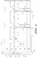
- FIG. 1is a partial cutaway side view of one embodiment of a wafer at one stage of its manufacture according to one embodiment of the present invention.
- wafer 101includes a semiconductor substrate 103 made of a bulk semiconductor material e.g. monocrystal silicon, gallium arsenide, or silicon germanium.
- a semiconductor substrateis a substrate that includes a semiconductor material.
- a semiconductor substratemay have other configurations such as a semiconductor on insulator (SOI) configuration. Examples of SOI configurations include a silicon-on-insulator (e.g. silicon oxide) on a bulk semiconductor material substrate and a silicon-on-sapphire substrate.
- SOI configurationsinclude a silicon-on-insulator (e.g. silicon oxide) on a bulk semiconductor material substrate and a silicon-on-sapphire substrate.
- a semiconductor substratemay include multiple layers of different semiconductor materials e.g.
- Substrate 103includes active circuitry (e.g. transistor 120 ) formed on the front side of substrate 103 .
- the front side of a wafer or substrateis the side of a wafer or substrate where the active circuitry is formed.
- the backside of a wafer or substrateis the side of the wafer or substrate opposite from the front side.
- Multilevel interconnect 122is formed on the front side 125 of wafer 101 .
- Multilevel interconnect 122includes interlevel dielectric layers 106 and 110 .
- Multilevel interconnect 122also includes interconnect layers 108 and 112 .
- Interlevel dielectric layers 106 and 110include dielectric material e.g. TEOS, SiO 2 , or low K dielectrics that electrically insulates metal interconnects of adjacent interconnect layers.
- Interlevel dielectric layers 106 and 110may also include etch stop layers and barrier layers e.g. made of materials as silicon nitride or silicon carbon nitride. The etch stop layers and barrier layers are not shown in FIG. 1 .
- Interlevel dielectric layers 106 and 110also include conductive vias 105 , 109 , 115 , and 121 having a conductive filler material of e.g. copper, tungsten, gold, and/or aluminum.
- the conductive viasinterconnect active circuitry (e.g. 120 ) on the front side of substrate 103 with the metal interconnects 107 , 111 , 113 , 117 , 119 , and 123 of interconnect layers 108 and 112 .
- Each interconnect layer ( 108 and 112 )also includes intralayer dielectric material ( 131 and 133 ) located between the metal interconnects (e.g. 107 and 113 ) of that interconnect layer.
- the dielectric material of the interconnect layers 106 and 110may also include etch stop layers and barrier layers (not shown).
- Metal interconnects 107 , 111 , 113 , 117 , 119 , and 123 of interconnect layers 108 and 112may be formed by forming a conductive layer over the front side 125 of wafer 101 and subsequently patterning the conductive layer.
- a layer of intra layer dielectric materiale.g. 131 , 133
- a metal layere.g. copper
- Front side 125is then planarized (e.g. by a chemical mechanical polishing (CMP)) wherein only the copper material remains in the trenches of the intra layer dielectric material.
- CMPchemical mechanical polishing
- a layer of metale.g. aluminum
- the metal layeris then patterned using photolithographic and etch processes to form the metal interconnects.
- Interlayer dielectric materialis then deposited over front side 125 wherein the intralayer dielectric material is then planarized using CMP or other planarization techniques such as resist coat and etch back.
- metal interconnectsmay also include multiple layers of different materials.
- a metal interconnectmay also include a conductive barrier layer (e.g. tantalum, tantalum nitride, titanium nitride, or titanium tungsten).
- Multilevel interconnect 122also includes a top dielectric layer 114 .
- layer 114includes a dielectric material e.g. silicon oxide, silicon oxynitride, silicon nitride, or polyimide.
- dielectric layer 114includes multiple dielectric layers and may include etch stop layers and barrier layers. Dielectric layer 114 includes openings to expose interconnects 111 , 117 and 123 of interconnect layer 112 .
- a metal layer 116is formed over front side 125 of wafer 101 .
- layer 116includes aluminum but may include other conductive material such as copper, gold, or tungsten.
- layer 116may include barrier or seed layers (e.g. titanium nitride, titanium tungsten, or tantalum).
- Layer 116may be formed by sputtering, CVD, plating, physical vapor deposition (PVD) or other processes. Layer 116 is a continuous conductive layer formed over all of front side 125 of wafer 101 . In one embodiment, layer 116 has a thickness in the range of 10,000 Angstroms to 50,000 Angstroms but may have other thicknesses in other embodiments.
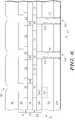
- FIG. 2is a partial cutaway side view of wafer 101 after substrate 103 has been thinned to reduce its thickness.
- Substrate 103may be thinned by grinding, etching, CMP, or by combinations of such processes.
- substrate 103has thickness in the range 300 microns to 1000 microns before thinning and a thickness in the range of 10 to 200 microns after thinning.
- wafers of other embodimentsmay have other thicknesses both before and after thinning.
- Dielectric layer 228is formed on backside 127 of wafer 101 .
- Dielectric layermay include silicon oxide, silicon nitride, TEOS, a diamond-like material, and/or sapphire.
- layer 228may be deposited (e.g. CVD, PVD) or grown from a substrate including semiconductor material on backside 127 . In some embodiments, layer 228 is not utilized.
- FIG. 3shows a partial cutaway side view of wafer 101 after openings or holes for vias 329 and 331 are formed from backside 127 of wafer 101 to interconnects 113 and 119 , respectively.
- the holes for vias 329 and 331are formed by forming a layer of photo resist over backside 127 and patterning the photo resist to form an etch mask for vias 329 and 331 .
- the material of dielectric layer 228 , substrate 103 , and the interlayer dielectric material of layer 106are etched using etch chemistries that are appropriate for removing the materials of those layers.
- the layer of patterned photo resist(not shown) is removed wherein layer 228 is used as a hard mask for subsequent etching of substrate 103 and layer 106 .
- the aspect ratio of the depth to width of the hole for vias 329 and 331is in the range of 0.5:1 to 10:1 but other aspect ratios may be utilized in other embodiments.
- side wall liners 401 and 403are formed on the sidewalls of vias 329 and 331 , respectively.
- liners 401 and 403are formed by depositing a conformal layer of spacer material (e.g. by CVD or atomic layer deposition (ALD)) and then anisotropically etching that conformal layer to leave liners 401 and 403 while exposing portions of interconnect 113 and 119 , respectively.
- liners 401 and 403are of a dielectric material (e.g.
- liners 401 and 403are of a material to act as a diffusion barrier for inhibiting diffusion of the metal filler material into substrate 103 .
- liners 401 and 403may be of a conductive material to electrically couple the filler material to the substrate. Such a configuration may be desirable for grounding substrate 103 . Other embodiments may not include liners 401 and 403 .
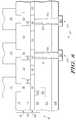
- FIG. 5shows a partial cutaway side view of wafer 101 during an electroplating process for the deposition of conductive filler material 507 and 509 in vias 329 and 331 , respectively.
- metal interconnects 113 and 119act as landing pads and seed layers for the electroplating of the conductive filler material 507 and 509 .
- a cathode connector 501is electrically connected to conductive metal layer 116 , which is electrically coupled to interconnect 113 though conductive via 115 and interconnect 117 and is electrically coupled to interconnect 119 through conductive via 121 and interconnect 123 .
- Cathode connector 501is electrically coupled to an electroplating power source 503 , which in the embodiment shown is a pulsed DC power source.
- An anode 505is electrically coupled to source 503 .
- wafer 101 and anode 505are submersed in an electrolyte plating solution and current from power source 503 sources current to connector 501 , where material from anode 505 is deposited in vias 329 and 331 .
- the filler materialinitially builds from interconnects 113 and 119 and continues to electroplate on the previously electroplated filler material.
- interconnects 113 and 119are electrically coupled to layer 116 , layer 116 acts as a current source during the electroplating for the formation of filler material 507 and 509 respectively.
- vias 329 and 331are shown as partially filled with conductive filler material 507 and 509 , respectively.
- Other electroplating processesmay be utilized in other embodiments.
- Layer 116may be protected or sealed during the electroplating process to avoid the deposition of material from anode 505 on that layer.
- the filler materialincludes copper but may include other material such as e.g. gold, nickel, palladium, alloys thereof or other platable conductive material.
- cathode connector 501is connected to layer 116 at a perimeter region of wafer 101 .
- the perimeter regionwould be a region of a wafer that would not be part of an integrated circuit upon singulation of the wafer into multiple integrated circuits.
- the region where cathode connector 501 attachesis on an area of layer 116 which is not subsequently used to form external connectors (e.g. bond pads) or other types of connectors of an integrated circuit.
- interconnects 113 and 119are the only exposed conductive structures shown in FIG. 5 electrically coupled to cathode connector 510 . Accordingly, filler material is only formed initially in vias 319 and 331 during the electroplating process. Accordingly, other structures are not plated with the conductive filler material. Accordingly, with this embodiment, the removal of a continuous layer of filler material on backside 127 after the electroplating process may not be required.
- FIG. 6shows wafer 101 after vias 329 and 331 have been completely filled with conductive filler material 601 and 603 , respectively.
- the electroplatingis performed to a point where the filler material overfills or begins to extend over some portion of dielectric layer 228 .
- backside 127would be planarized after electroplating to make filler material 601 and 603 co-planar with layer 228 .
- FIG. 7shows wafer 101 after layer 116 has been patterned to form conductive pads.
- layer 116is patterned by photolithographic and techniques. For example, a layer of photo resist may be deposited on front side 125 over layer 116 and patterned to form mask structures. All material of layer 116 not located under the mask structures would be removed to leave the pads.
- pads 701 , 703 , and 705are external wire bond pads. In another embodiment, pads 701 , 703 , and 705 are each under bump pad structures for a bump connector, where subsequent metal is formed on pads 701 , 703 , and 705 to complete the bump structure. These external conductors are used to electrically couple the circuitry of the integrated circuits of wafer 101 to external circuitry. In other embodiments, another integrated circuit may be electrically coupled to pads 701 , 703 , and 705 , such as in a multiple die package configuration (e.g. as in vertical or 3-D integration).
- One advantage that may occur from utilizing a metal layer, that is used to form the external connectors, for cathode connector attachmentis that additional interlevel metal layer deposition is not require after the thinning of the wafer for backside via formation.
- additional interlevel metal layer depositionis not require after the thinning of the wafer for backside via formation.
- subsequent metal layer depositionis needed to interconnect the circuitry of the wafer.
- Such depositionis made more complex by the reduction of substrate thickness.
- all front side interlevel metal layersare deposited prior to wafer thinning.
- interconnect levelsmay be added on top of pads 701 , 703 and 705 to further interconnect the active circuitry of the substrate 103 with structures for external electrical connection.
- another metal layermay be deposited and patterned on front side 125 for the interconnection of pads 701 , 703 , and 705 .
- an interconnect utilized as a seed layere.g. interconnect 119 ) for the formation of a conductive via may not be electrically coupled to an external electrical connector.
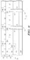
- FIG. 8shows a partial cutaway side view of wafer 101 after backside connector pads 801 and 803 are formed.
- Pads 801 and 803are electrically coupled to filler material 601 and 603 , respectively.
- pad 801is electrically coupled to pad 703 and pad 803 is electrically coupled to pad 705 .
- connector pads 801 and 803are formed by the deposition of a metal layer and photolithographic and etch patterning of the metal layer. In other embodiments, pads 801 and 803 are formed by an in-laid process where a dielectric layer is deposited and openings for the pads are formed. A metal layer is then deposited over backside 127 including in the openings and then is planarized where the metal located outside the openings is removed.
- pads 801 and 803may be formed by depositing a seed conductive layer over backside 127 , forming a layer of photo resist over the seed layer with openings for the pads, and then electroplating material in the openings. In subsequent processes, the photo resist and seed layer external to the pads would be removed. In still another embodiment, pads 801 and 803 would be formed by selective deposition of metal on the conductive filler material 601 and 603 .
- pads 801 and 803may be formed prior to the patterning of layer 116 . Other embodiments do not include pads 801 and 803 . Still in other embodiments, at least a portion of layer 228 may be removed after the formation of filler material 601 and 603 such that a portion of filler material 601 and 603 extends out from backside 127 .
- pads 801 and 803are utilized for external connection of the circuitry of the integrated circuits of wafer 101 to external circuitry.
- FIG. 9shows a second embodiment of wafer 101 .
- the embodiment of FIG. 9is different from the embodiment of FIG. 7 in that pads 901 , 903 , and 905 are patterned from metal layer 116 by an in-laid process as opposed to a patterning process for forming pads 701 , 703 , and 705 of FIG. 7 .
- layer 116is planarized (e.g. by a CMP process) such that the material of layer 116 external to the openings in layer 114 is removed.
- additional structurese.g. pads 801 and 803
- Wafer 101includes other active circuitry, interconnects, and through substrate conductive vias (not shown) located at other regions of wafer 101 . Wafer 101 may be subsequently singulated into multiple integrated circuits. The integrated circuits may then be packaged into integrated circuit packages wherein the pads (e.g. 701 , 801 , and 901 ) are electrically coupled to conductive structures of the package. In one embodiment, the integrated circuits maybe part of multi integrated circuit packages.
- the seed layers for electroplatingare located in the first formed interconnect layer 108 of multilevel interconnect 122 .
- the seed layersmay be located in other metal layers (e.g. 112 ) formed subsequently to layer 108 .
- One advantage that may occur from utilizing an interior conductive interconnect (e.g. 113 and 119 ) as a landing pad and seed layer for conductive via formationis that it reduces the amount of the thickness of wafer 101 that has to be removed in the formation of vias 329 and 331 as compared to a via that is formed all the way through a wafer 101 .
- a reduction in the amount of wafer removed for a through substrate vianot only reduces etching time, it also reduces the number of etching steps in that the number of layers of different material is reduced. For example, because not all of the layers of multilayer interconnect 122 are removed, less etching processes are needed to make vias 329 and 331 .
- the utilization of layer that will be used to form subsequent conductive structures of an integrated circuit (e.g. 116 ) as a cathode connector contact layer and current sourcefurther reduces the number of processing steps needed for electroplating to form a backside via connection. Because layer 116 will be subsequently used to form electrical connectors for the integrated circuits of wafer 101 , the electroplating will not require an addition step of seed layer formation and removal as with other electroplating via formation methods.
- a front side metal layeras a cathode connector contact layer allows for build up of the conductive via filler material from the backside of a wafer without having to deposit a seed layer into the via hole from the backside. Accordingly, voids and bread loafing of the seed layer material into the via can be avoided.
- vias with a higher aspect ratiomay be formed using processes described herein.
- planarization processesmay be efficiently utilized in removing the over plated filler material in that a seed layer does not also have to be removed in the planarization process.
- electroplating for conductive via filler material depositionallows the via to be filled from an internal conductor to the backside thereby reducing void and bread loafing that may occur from conformal layer filler material deposition. Accordingly, higher aspect ratio via formation may be utilized.
- material formationoccurs mainly in the via hole and not outside of the via hole. This may advantageously reduce the amount of excess filler material that is to be removed after the via has been filled with conductive material.
- the exposed portion of the seed layerse.g. patterned interconnects 119 and 113
- the material build up rate during electroplatingis enhanced as compared to processes that electroplate over a seed layer covering an entire wafer. Because the seed layer is only located in areas of material formation, the amount of area to electroplate is reduced and that area is electroplated at a faster rate. Thus, having patterned structures as seed layers reduces plating time.
- the method described hereinmay also be utilized to electroplate from a front side of a wafer as well.
- One embodimentincludes a method for forming a conductive via.
- the methodincludes forming a conductive layer over a first side of a semiconductor substrate.
- the semiconductor substratecomprises a first side and a second side and the first side is opposite the second side.
- the methodalso includes patterning the conductive layer to form a landing pad and forming a via hole in the semiconductor substrate from the second side of the semiconductor substrate.
- the via holeexposes the landing pad.
- the methodalso includes electroplating a conductive via material in the via hole using the landing pad as a seed layer.
- Another embodimentincludes a method for forming a conductive via.
- the methodincludes forming a seed layer over a first side of a semiconductor substrate.
- the semiconductor substratecomprises a first side and a second side and the first side is opposite the second side.
- the methodalso includes forming a continuous conductive layer over the seed layer.
- the seed layeris electrically coupled to the continuous conductive layer.
- the methodfurther includes after forming the seed layer, forming a via hole in the semiconductor substrate from the second side of the semiconductor substrate.
- the via holeexposes the seed layer.
- the methodalso includes electroplating a conductive via material from the seed layer in the via hole using the continuous conductive layer as a current source.
- Another embodimentincludes a method for forming a conductive via.
- the methodincludes forming a conductive layer over a first side of a semiconductor substrate.
- the semiconductor substratecomprises a first side and a second side. The first side is opposite the second side.
- the semiconductor substratecomprises active circuitry.
- the methodalso includes patterning the conductive layer to form a landing pad and forming a continuous conductive layer over the landing pad.
- the continuous conductive layeris electrically coupled to the landing pad.
- the methodalso includes etching the semiconductor substrate from the second side to form a via hole and expose the landing pad and electroplating a conductive via material in the via hole using the landing pad as a seed layer and the continuous conductive layer as a current source.
- the methodalso includes patterning the continuous conductive layer after electroplating the conductive via material.
Landscapes
- Engineering & Computer Science (AREA)
- Physics & Mathematics (AREA)
- Condensed Matter Physics & Semiconductors (AREA)
- General Physics & Mathematics (AREA)
- Manufacturing & Machinery (AREA)
- Computer Hardware Design (AREA)
- Microelectronics & Electronic Packaging (AREA)
- Power Engineering (AREA)
- Internal Circuitry In Semiconductor Integrated Circuit Devices (AREA)
- Electroplating Methods And Accessories (AREA)
Abstract
Description
Claims (22)
Priority Applications (5)
| Application Number | Priority Date | Filing Date | Title |
|---|---|---|---|
| US11/679,512US7741218B2 (en) | 2007-02-27 | 2007-02-27 | Conductive via formation utilizing electroplating |
| JP2009551767AJP5366833B2 (en) | 2007-02-27 | 2008-01-25 | Conductive via formation using electroplating |
| CN2008800064171ACN101622700B (en) | 2007-02-27 | 2008-01-25 | Utilizes plated conductive via formation |
| PCT/US2008/051987WO2008106256A1 (en) | 2007-02-27 | 2008-01-25 | Conductive via formation utilizing electroplating |
| TW097105225ATWI483312B (en) | 2007-02-27 | 2008-02-14 | Conductive via formation utilizing electroplating |
Applications Claiming Priority (1)
| Application Number | Priority Date | Filing Date | Title |
|---|---|---|---|
| US11/679,512US7741218B2 (en) | 2007-02-27 | 2007-02-27 | Conductive via formation utilizing electroplating |
Publications (2)
| Publication Number | Publication Date |
|---|---|
| US20080206984A1 US20080206984A1 (en) | 2008-08-28 |
| US7741218B2true US7741218B2 (en) | 2010-06-22 |
Family
ID=39716386
Family Applications (1)
| Application Number | Title | Priority Date | Filing Date |
|---|---|---|---|
| US11/679,512Active2027-12-15US7741218B2 (en) | 2007-02-27 | 2007-02-27 | Conductive via formation utilizing electroplating |
Country Status (5)
| Country | Link |
|---|---|
| US (1) | US7741218B2 (en) |
| JP (1) | JP5366833B2 (en) |
| CN (1) | CN101622700B (en) |
| TW (1) | TWI483312B (en) |
| WO (1) | WO2008106256A1 (en) |
Cited By (6)
| Publication number | Priority date | Publication date | Assignee | Title |
|---|---|---|---|---|
| US8654541B2 (en) | 2011-03-24 | 2014-02-18 | Toyota Motor Engineering & Manufacturing North America, Inc. | Three-dimensional power electronics packages |
| US9105628B1 (en)* | 2012-03-29 | 2015-08-11 | Valery Dubin | Through substrate via (TSuV) structures and method of making the same |
| US9219032B2 (en) | 2012-07-09 | 2015-12-22 | Qualcomm Incorporated | Integrating through substrate vias from wafer backside layers of integrated circuits |
| US10699954B2 (en) | 2018-04-19 | 2020-06-30 | Teledyne Scientific & Imaging, Llc | Through-substrate vias formed by bottom-up electroplating |
| US11721628B2 (en) | 2019-07-23 | 2023-08-08 | Samsung Electronics Co., Ltd. | Semiconductor device |
| US11949008B2 (en) | 2020-12-30 | 2024-04-02 | Win Semiconductors Corp. | Semiconductor structure and method for forming the same |
Families Citing this family (12)
| Publication number | Priority date | Publication date | Assignee | Title |
|---|---|---|---|---|
| US7939941B2 (en)* | 2007-06-27 | 2011-05-10 | Taiwan Semiconductor Manufacturing Company, Ltd. | Formation of through via before contact processing |
| US7872357B2 (en)* | 2008-03-05 | 2011-01-18 | Taiwan Semiconductor Manufacturing Company, Ltd. | Protection for bonding pads and methods of formation |
| US8853830B2 (en) | 2008-05-14 | 2014-10-07 | Taiwan Semiconductor Manufacturing Company, Ltd. | System, structure, and method of manufacturing a semiconductor substrate stack |
| US8691664B2 (en)* | 2009-04-20 | 2014-04-08 | Taiwan Semiconductor Manufacturing Company, Ltd. | Backside process for a substrate |
| TWI471977B (en)* | 2009-05-15 | 2015-02-01 | Xintec Inc | Power MOS half field effect transistor package |
| TWI504780B (en)* | 2009-09-04 | 2015-10-21 | Win Semiconductors Corp | A method of using an electroless plating for depositing a metal seed layer on semiconductor chips for the backside and via-hole manufacturing processes |
| US8304863B2 (en) | 2010-02-09 | 2012-11-06 | International Business Machines Corporation | Electromigration immune through-substrate vias |
| US9159699B2 (en)* | 2012-11-13 | 2015-10-13 | Delta Electronics, Inc. | Interconnection structure having a via structure |
| JP6104772B2 (en)* | 2013-03-29 | 2017-03-29 | ソニーセミコンダクタソリューションズ株式会社 | Laminated structure and manufacturing method thereof |
| US9754883B1 (en)* | 2016-03-04 | 2017-09-05 | International Business Machines Corporation | Hybrid metal interconnects with a bamboo grain microstructure |
| US10432172B2 (en)* | 2016-09-01 | 2019-10-01 | Samsung Electro-Mechanics Co., Ltd. | Bulk acoustic filter device and method of manufacturing the same |
| JP6877290B2 (en)* | 2017-08-03 | 2021-05-26 | 東京エレクトロン株式会社 | How to process the object to be processed |
Citations (7)
| Publication number | Priority date | Publication date | Assignee | Title |
|---|---|---|---|---|
| JPH08279510A (en) | 1995-04-04 | 1996-10-22 | Murata Mfg Co Ltd | Method of manufacturing semiconductor device |
| US6221769B1 (en) | 1999-03-05 | 2001-04-24 | International Business Machines Corporation | Method for integrated circuit power and electrical connections via through-wafer interconnects |
| US20040173909A1 (en)* | 2003-03-05 | 2004-09-09 | Micron Technology, Inc. | Conductive through wafer vias |
| US7109068B2 (en) | 2004-08-31 | 2006-09-19 | Micron Technology, Inc. | Through-substrate interconnect fabrication methods |
| US7179738B2 (en) | 2004-06-17 | 2007-02-20 | Texas Instruments Incorporated | Semiconductor assembly having substrate with electroplated contact pads |
| US20070045780A1 (en)* | 2005-09-01 | 2007-03-01 | Salman Akram | Methods of forming blind wafer interconnects, and related structures and assemblies |
| US20080166874A1 (en)* | 2007-01-05 | 2008-07-10 | International Business Machines Corporation | Formation of vertical devices by electroplating |
Family Cites Families (3)
| Publication number | Priority date | Publication date | Assignee | Title |
|---|---|---|---|---|
| JPH11135506A (en)* | 1997-10-31 | 1999-05-21 | Nec Corp | Manufacture of semiconductor device |
| JP2006210369A (en)* | 2005-01-25 | 2006-08-10 | Murata Mfg Co Ltd | Semiconductor apparatus and manufacturing method thereof |
| JP2007049103A (en)* | 2005-08-05 | 2007-02-22 | Zycube:Kk | Semiconductor chip, manufacturing method thereof, and semiconductor device |
- 2007
- 2007-02-27USUS11/679,512patent/US7741218B2/enactiveActive
- 2008
- 2008-01-25JPJP2009551767Apatent/JP5366833B2/enactiveActive
- 2008-01-25WOPCT/US2008/051987patent/WO2008106256A1/enactiveApplication Filing
- 2008-01-25CNCN2008800064171Apatent/CN101622700B/enactiveActive
- 2008-02-14TWTW097105225Apatent/TWI483312B/enactive
Patent Citations (7)
| Publication number | Priority date | Publication date | Assignee | Title |
|---|---|---|---|---|
| JPH08279510A (en) | 1995-04-04 | 1996-10-22 | Murata Mfg Co Ltd | Method of manufacturing semiconductor device |
| US6221769B1 (en) | 1999-03-05 | 2001-04-24 | International Business Machines Corporation | Method for integrated circuit power and electrical connections via through-wafer interconnects |
| US20040173909A1 (en)* | 2003-03-05 | 2004-09-09 | Micron Technology, Inc. | Conductive through wafer vias |
| US7179738B2 (en) | 2004-06-17 | 2007-02-20 | Texas Instruments Incorporated | Semiconductor assembly having substrate with electroplated contact pads |
| US7109068B2 (en) | 2004-08-31 | 2006-09-19 | Micron Technology, Inc. | Through-substrate interconnect fabrication methods |
| US20070045780A1 (en)* | 2005-09-01 | 2007-03-01 | Salman Akram | Methods of forming blind wafer interconnects, and related structures and assemblies |
| US20080166874A1 (en)* | 2007-01-05 | 2008-07-10 | International Business Machines Corporation | Formation of vertical devices by electroplating |
Non-Patent Citations (7)
| Title |
|---|
| Hauffe et al; "Optimized Micro-Via Technology for High Density and High Frequency (>40GHz) Hermetic Through-Wafer Connections in Silicon Substrates"; 2005 IEEE Electronic Components and Technology Conference; pp. 324-330. |
| International Search Report and Written Opinion for PCT Patent Application No. PCT/US2008/051987, dated May 27, 2008. |
| Morrow et al; "Three-Dimensional Wafer Stacking via Cu-Cu Bonding Intergrated with 65-nm Strained-Si/Low-k CMOS Technology"; IEEE Electron Device Letters, vol. 27, No. 5, May 2006. |
| Nguyen et al; "Through-Wafer Copper Electroplating for RF Silicon Technology"; ESSDERC, 2002, pp. 255-258. |
| Nguyen et al; "Through-Wafer Copper Electroplating for Three-Dimensional Interconnects"; J. of Micromechanics and Microengineering, 12 (2002), pp. 395-399. |
| Premachandran et al; "A Novel Electrically Conductive Wafer Through Hole Filled Vias Interconnect for 3D MEMS Packaging"; 2003 IEEE Electronic Components and Technology Conference; pp. 627-630. |
| Wu et al; "A Through-Wafer Interconnect in Silicon for RFICs"; IEEE Transactions on Electron Devices, vol. 51, No. 11, Nov. 2004, pp. 1765-1771. |
Cited By (6)
| Publication number | Priority date | Publication date | Assignee | Title |
|---|---|---|---|---|
| US8654541B2 (en) | 2011-03-24 | 2014-02-18 | Toyota Motor Engineering & Manufacturing North America, Inc. | Three-dimensional power electronics packages |
| US9105628B1 (en)* | 2012-03-29 | 2015-08-11 | Valery Dubin | Through substrate via (TSuV) structures and method of making the same |
| US9219032B2 (en) | 2012-07-09 | 2015-12-22 | Qualcomm Incorporated | Integrating through substrate vias from wafer backside layers of integrated circuits |
| US10699954B2 (en) | 2018-04-19 | 2020-06-30 | Teledyne Scientific & Imaging, Llc | Through-substrate vias formed by bottom-up electroplating |
| US11721628B2 (en) | 2019-07-23 | 2023-08-08 | Samsung Electronics Co., Ltd. | Semiconductor device |
| US11949008B2 (en) | 2020-12-30 | 2024-04-02 | Win Semiconductors Corp. | Semiconductor structure and method for forming the same |
Also Published As
| Publication number | Publication date |
|---|---|
| JP5366833B2 (en) | 2013-12-11 |
| US20080206984A1 (en) | 2008-08-28 |
| JP2010519780A (en) | 2010-06-03 |
| TW200850102A (en) | 2008-12-16 |
| WO2008106256A1 (en) | 2008-09-04 |
| TWI483312B (en) | 2015-05-01 |
| CN101622700B (en) | 2011-05-25 |
| CN101622700A (en) | 2010-01-06 |
Similar Documents
| Publication | Publication Date | Title |
|---|---|---|
| US7741218B2 (en) | Conductive via formation utilizing electroplating | |
| CN108461477B (en) | Metal interconnect for ultra (skip) via integration | |
| US9805972B1 (en) | Skip via structures | |
| US6821879B2 (en) | Copper interconnect by immersion/electroless plating in dual damascene process | |
| US7446036B1 (en) | Gap free anchored conductor and dielectric structure and method for fabrication thereof | |
| US10037940B2 (en) | Reliable packaging and interconnect structures | |
| US20080113505A1 (en) | Method of forming a through-substrate via | |
| US6534865B1 (en) | Method of enhanced fill of vias and trenches | |
| KR101577959B1 (en) | Method for forming electric wiring using electroless plating method for preventing void formation | |
| US9666529B2 (en) | Method and structure to reduce the electric field in semiconductor wiring interconnects | |
| US9761528B2 (en) | Interconnection structure | |
| US8227340B2 (en) | Method for producing a copper connection between two sides of a substrate | |
| US20100072579A1 (en) | Through Substrate Conductors | |
| US20200144195A1 (en) | Silicon carbide and silicon nitride interconnects | |
| US9978666B2 (en) | Method for fabrication semiconductor device with through-substrate via | |
| US20020111013A1 (en) | Method for formation of single inlaid structures | |
| US6811670B2 (en) | Method for forming cathode contact areas for an electroplating process | |
| US7928570B2 (en) | Interconnect structure | |
| US6368965B1 (en) | Method for low stress plating of semiconductor vias and channels | |
| US6518171B1 (en) | Dual damascene process using a low k interlayer for forming vias and trenches | |
| US20240105607A1 (en) | Buried power rail directly contacting backside power delivery network | |
| CN111383990B (en) | Semiconductor structure and forming method thereof | |
| US20250157927A1 (en) | Low resistance signal transduction enabled by high efficiency copper feedthroughs | |
| KR20070066298A (en) | Metal wiring of semiconductor device and manufacturing method thereof | |
| US7981781B2 (en) | Metal line of semiconductor device having a diffusion barrier and method for forming the same |
Legal Events
| Date | Code | Title | Description |
|---|---|---|---|
| AS | Assignment | Owner name:FREESCALE SEMICONDUCTOR, INC.,TEXAS Free format text:ASSIGNMENT OF ASSIGNORS INTEREST;ASSIGNORS:SPARKS, TERRY G.;JONES, ROBERT E.;REEL/FRAME:018937/0555 Effective date:20070227 | |
| AS | Assignment | Owner name:CITIBANK, N.A., NEW YORK Free format text:SECURITY AGREEMENT;ASSIGNOR:FREESCALE SEMICONDUCTOR, INC.;REEL/FRAME:019847/0804 Effective date:20070620 Owner name:CITIBANK, N.A.,NEW YORK Free format text:SECURITY AGREEMENT;ASSIGNOR:FREESCALE SEMICONDUCTOR, INC.;REEL/FRAME:019847/0804 Effective date:20070620 | |
| AS | Assignment | Owner name:CITIBANK, N.A., NEW YORK Free format text:SECURITY AGREEMENT;ASSIGNOR:FREESCALE SEMICONDUCTOR, INC.;REEL/FRAME:024085/0001 Effective date:20100219 Owner name:CITIBANK, N.A.,NEW YORK Free format text:SECURITY AGREEMENT;ASSIGNOR:FREESCALE SEMICONDUCTOR, INC.;REEL/FRAME:024085/0001 Effective date:20100219 | |
| AS | Assignment | Owner name:CITIBANK, N.A., AS COLLATERAL AGENT, NEW YORK Free format text:SECURITY AGREEMENT;ASSIGNOR:FREESCALE SEMICONDUCTOR, INC.;REEL/FRAME:024397/0001 Effective date:20100413 Owner name:CITIBANK, N.A., AS COLLATERAL AGENT,NEW YORK Free format text:SECURITY AGREEMENT;ASSIGNOR:FREESCALE SEMICONDUCTOR, INC.;REEL/FRAME:024397/0001 Effective date:20100413 | |
| STCF | Information on status: patent grant | Free format text:PATENTED CASE | |
| AS | Assignment | Owner name:CITIBANK, N.A., AS NOTES COLLATERAL AGENT, NEW YORK Free format text:SECURITY AGREEMENT;ASSIGNOR:FREESCALE SEMICONDUCTOR, INC.;REEL/FRAME:030633/0424 Effective date:20130521 Owner name:CITIBANK, N.A., AS NOTES COLLATERAL AGENT, NEW YOR Free format text:SECURITY AGREEMENT;ASSIGNOR:FREESCALE SEMICONDUCTOR, INC.;REEL/FRAME:030633/0424 Effective date:20130521 | |
| AS | Assignment | Owner name:CITIBANK, N.A., AS NOTES COLLATERAL AGENT, NEW YORK Free format text:SECURITY AGREEMENT;ASSIGNOR:FREESCALE SEMICONDUCTOR, INC.;REEL/FRAME:031591/0266 Effective date:20131101 Owner name:CITIBANK, N.A., AS NOTES COLLATERAL AGENT, NEW YOR Free format text:SECURITY AGREEMENT;ASSIGNOR:FREESCALE SEMICONDUCTOR, INC.;REEL/FRAME:031591/0266 Effective date:20131101 | |
| FPAY | Fee payment | Year of fee payment:4 | |
| AS | Assignment | Owner name:FREESCALE SEMICONDUCTOR, INC., TEXAS Free format text:PATENT RELEASE;ASSIGNOR:CITIBANK, N.A., AS COLLATERAL AGENT;REEL/FRAME:037356/0143 Effective date:20151207 Owner name:FREESCALE SEMICONDUCTOR, INC., TEXAS Free format text:PATENT RELEASE;ASSIGNOR:CITIBANK, N.A., AS COLLATERAL AGENT;REEL/FRAME:037354/0640 Effective date:20151207 Owner name:FREESCALE SEMICONDUCTOR, INC., TEXAS Free format text:PATENT RELEASE;ASSIGNOR:CITIBANK, N.A., AS COLLATERAL AGENT;REEL/FRAME:037356/0553 Effective date:20151207 | |
| AS | Assignment | Owner name:MORGAN STANLEY SENIOR FUNDING, INC., MARYLAND Free format text:ASSIGNMENT AND ASSUMPTION OF SECURITY INTEREST IN PATENTS;ASSIGNOR:CITIBANK, N.A.;REEL/FRAME:037486/0517 Effective date:20151207 | |
| AS | Assignment | Owner name:MORGAN STANLEY SENIOR FUNDING, INC., MARYLAND Free format text:ASSIGNMENT AND ASSUMPTION OF SECURITY INTEREST IN PATENTS;ASSIGNOR:CITIBANK, N.A.;REEL/FRAME:037518/0292 Effective date:20151207 | |
| AS | Assignment | Owner name:MORGAN STANLEY SENIOR FUNDING, INC., MARYLAND Free format text:SUPPLEMENT TO THE SECURITY AGREEMENT;ASSIGNOR:FREESCALE SEMICONDUCTOR, INC.;REEL/FRAME:039138/0001 Effective date:20160525 | |
| AS | Assignment | Owner name:NXP, B.V., F/K/A FREESCALE SEMICONDUCTOR, INC., NETHERLANDS Free format text:RELEASE BY SECURED PARTY;ASSIGNOR:MORGAN STANLEY SENIOR FUNDING, INC.;REEL/FRAME:040925/0001 Effective date:20160912 Owner name:NXP, B.V., F/K/A FREESCALE SEMICONDUCTOR, INC., NE Free format text:RELEASE BY SECURED PARTY;ASSIGNOR:MORGAN STANLEY SENIOR FUNDING, INC.;REEL/FRAME:040925/0001 Effective date:20160912 | |
| AS | Assignment | Owner name:NXP B.V., NETHERLANDS Free format text:RELEASE BY SECURED PARTY;ASSIGNOR:MORGAN STANLEY SENIOR FUNDING, INC.;REEL/FRAME:040928/0001 Effective date:20160622 | |
| AS | Assignment | Owner name:NXP USA, INC., TEXAS Free format text:CHANGE OF NAME;ASSIGNOR:FREESCALE SEMICONDUCTOR, INC.;REEL/FRAME:040632/0001 Effective date:20161107 | |
| AS | Assignment | Owner name:MORGAN STANLEY SENIOR FUNDING, INC., MARYLAND Free format text:CORRECTIVE ASSIGNMENT TO CORRECT THE REMOVE PATENTS 8108266 AND 8062324 AND REPLACE THEM WITH 6108266 AND 8060324 PREVIOUSLY RECORDED ON REEL 037518 FRAME 0292. ASSIGNOR(S) HEREBY CONFIRMS THE ASSIGNMENT AND ASSUMPTION OF SECURITY INTEREST IN PATENTS;ASSIGNOR:CITIBANK, N.A.;REEL/FRAME:041703/0536 Effective date:20151207 | |
| MAFP | Maintenance fee payment | Free format text:PAYMENT OF MAINTENANCE FEE, 8TH YEAR, LARGE ENTITY (ORIGINAL EVENT CODE: M1552) Year of fee payment:8 | |
| AS | Assignment | Owner name:NXP USA, INC., TEXAS Free format text:CORRECTIVE ASSIGNMENT TO CORRECT THE NATURE OF CONVEYANCE PREVIOUSLY RECORDED AT REEL: 040632 FRAME: 0001. ASSIGNOR(S) HEREBY CONFIRMS THE MERGER AND CHANGE OF NAME;ASSIGNOR:FREESCALE SEMICONDUCTOR INC.;REEL/FRAME:044209/0047 Effective date:20161107 | |
| AS | Assignment | Owner name:SHENZHEN XINGUODU TECHNOLOGY CO., LTD., CHINA Free format text:CORRECTIVE ASSIGNMENT TO CORRECT THE TO CORRECT THE APPLICATION NO. FROM 13,883,290 TO 13,833,290 PREVIOUSLY RECORDED ON REEL 041703 FRAME 0536. ASSIGNOR(S) HEREBY CONFIRMS THE THE ASSIGNMENT AND ASSUMPTION OF SECURITYINTEREST IN PATENTS.;ASSIGNOR:MORGAN STANLEY SENIOR FUNDING, INC.;REEL/FRAME:048734/0001 Effective date:20190217 | |
| AS | Assignment | Owner name:NXP B.V., NETHERLANDS Free format text:RELEASE BY SECURED PARTY;ASSIGNOR:MORGAN STANLEY SENIOR FUNDING, INC.;REEL/FRAME:050744/0097 Effective date:20190903 | |
| AS | Assignment | Owner name:MORGAN STANLEY SENIOR FUNDING, INC., MARYLAND Free format text:CORRECTIVE ASSIGNMENT TO CORRECT THE REMOVE APPLICATION11759915 AND REPLACE IT WITH APPLICATION 11759935 PREVIOUSLY RECORDED ON REEL 037486 FRAME 0517. ASSIGNOR(S) HEREBY CONFIRMS THE ASSIGNMENT AND ASSUMPTION OF SECURITYINTEREST IN PATENTS;ASSIGNOR:CITIBANK, N.A.;REEL/FRAME:053547/0421 Effective date:20151207 | |
| AS | Assignment | Owner name:NXP B.V., NETHERLANDS Free format text:CORRECTIVE ASSIGNMENT TO CORRECT THE REMOVEAPPLICATION 11759915 AND REPLACE IT WITH APPLICATION11759935 PREVIOUSLY RECORDED ON REEL 040928 FRAME 0001. ASSIGNOR(S) HEREBY CONFIRMS THE RELEASE OF SECURITYINTEREST;ASSIGNOR:MORGAN STANLEY SENIOR FUNDING, INC.;REEL/FRAME:052915/0001 Effective date:20160622 | |
| AS | Assignment | Owner name:NXP, B.V. F/K/A FREESCALE SEMICONDUCTOR, INC., NETHERLANDS Free format text:CORRECTIVE ASSIGNMENT TO CORRECT THE REMOVEAPPLICATION 11759915 AND REPLACE IT WITH APPLICATION11759935 PREVIOUSLY RECORDED ON REEL 040925 FRAME 0001. ASSIGNOR(S) HEREBY CONFIRMS THE RELEASE OF SECURITYINTEREST;ASSIGNOR:MORGAN STANLEY SENIOR FUNDING, INC.;REEL/FRAME:052917/0001 Effective date:20160912 | |
| MAFP | Maintenance fee payment | Free format text:PAYMENT OF MAINTENANCE FEE, 12TH YEAR, LARGE ENTITY (ORIGINAL EVENT CODE: M1553); ENTITY STATUS OF PATENT OWNER: LARGE ENTITY Year of fee payment:12 |