US7741150B2 - Packaged microelectronic devices and methods for manufacturing packaged microelectronic devices - Google Patents
Packaged microelectronic devices and methods for manufacturing packaged microelectronic devicesDownload PDFInfo
- Publication number
- US7741150B2 US7741150B2US11/626,683US62668307AUS7741150B2US 7741150 B2US7741150 B2US 7741150B2US 62668307 AUS62668307 AUS 62668307AUS 7741150 B2US7741150 B2US 7741150B2
- Authority
- US
- United States
- Prior art keywords
- die
- stand
- layer
- dies
- attaching
- Prior art date
- Legal status (The legal status is an assumption and is not a legal conclusion. Google has not performed a legal analysis and makes no representation as to the accuracy of the status listed.)
- Active, expires
Links
Images


Classifications
- H—ELECTRICITY
- H01—ELECTRIC ELEMENTS
- H01L—SEMICONDUCTOR DEVICES NOT COVERED BY CLASS H10
- H01L24/00—Arrangements for connecting or disconnecting semiconductor or solid-state bodies; Methods or apparatus related thereto
- H01L24/01—Means for bonding being attached to, or being formed on, the surface to be connected, e.g. chip-to-package, die-attach, "first-level" interconnects; Manufacturing methods related thereto
- H01L24/42—Wire connectors; Manufacturing methods related thereto
- H01L24/47—Structure, shape, material or disposition of the wire connectors after the connecting process
- H01L24/49—Structure, shape, material or disposition of the wire connectors after the connecting process of a plurality of wire connectors
- H—ELECTRICITY
- H01—ELECTRIC ELEMENTS
- H01L—SEMICONDUCTOR DEVICES NOT COVERED BY CLASS H10
- H01L21/00—Processes or apparatus adapted for the manufacture or treatment of semiconductor or solid state devices or of parts thereof
- H01L21/02—Manufacture or treatment of semiconductor devices or of parts thereof
- H01L21/04—Manufacture or treatment of semiconductor devices or of parts thereof the devices having potential barriers, e.g. a PN junction, depletion layer or carrier concentration layer
- H01L21/50—Assembly of semiconductor devices using processes or apparatus not provided for in a single one of the groups H01L21/18 - H01L21/326 or H10D48/04 - H10D48/07 e.g. sealing of a cap to a base of a container
- H01L21/56—Encapsulations, e.g. encapsulation layers, coatings
- H01L21/561—Batch processing
- H—ELECTRICITY
- H01—ELECTRIC ELEMENTS
- H01L—SEMICONDUCTOR DEVICES NOT COVERED BY CLASS H10
- H01L21/00—Processes or apparatus adapted for the manufacture or treatment of semiconductor or solid state devices or of parts thereof
- H01L21/67—Apparatus specially adapted for handling semiconductor or electric solid state devices during manufacture or treatment thereof; Apparatus specially adapted for handling wafers during manufacture or treatment of semiconductor or electric solid state devices or components ; Apparatus not specifically provided for elsewhere
- H01L21/683—Apparatus specially adapted for handling semiconductor or electric solid state devices during manufacture or treatment thereof; Apparatus specially adapted for handling wafers during manufacture or treatment of semiconductor or electric solid state devices or components ; Apparatus not specifically provided for elsewhere for supporting or gripping
- H01L21/6835—Apparatus specially adapted for handling semiconductor or electric solid state devices during manufacture or treatment thereof; Apparatus specially adapted for handling wafers during manufacture or treatment of semiconductor or electric solid state devices or components ; Apparatus not specifically provided for elsewhere for supporting or gripping using temporarily an auxiliary support
- H—ELECTRICITY
- H01—ELECTRIC ELEMENTS
- H01L—SEMICONDUCTOR DEVICES NOT COVERED BY CLASS H10
- H01L24/00—Arrangements for connecting or disconnecting semiconductor or solid-state bodies; Methods or apparatus related thereto
- H01L24/01—Means for bonding being attached to, or being formed on, the surface to be connected, e.g. chip-to-package, die-attach, "first-level" interconnects; Manufacturing methods related thereto
- H01L24/26—Layer connectors, e.g. plate connectors, solder or adhesive layers; Manufacturing methods related thereto
- H01L24/27—Manufacturing methods
- H—ELECTRICITY
- H01—ELECTRIC ELEMENTS
- H01L—SEMICONDUCTOR DEVICES NOT COVERED BY CLASS H10
- H01L24/00—Arrangements for connecting or disconnecting semiconductor or solid-state bodies; Methods or apparatus related thereto
- H01L24/01—Means for bonding being attached to, or being formed on, the surface to be connected, e.g. chip-to-package, die-attach, "first-level" interconnects; Manufacturing methods related thereto
- H01L24/26—Layer connectors, e.g. plate connectors, solder or adhesive layers; Manufacturing methods related thereto
- H01L24/28—Structure, shape, material or disposition of the layer connectors prior to the connecting process
- H01L24/29—Structure, shape, material or disposition of the layer connectors prior to the connecting process of an individual layer connector
- H—ELECTRICITY
- H01—ELECTRIC ELEMENTS
- H01L—SEMICONDUCTOR DEVICES NOT COVERED BY CLASS H10
- H01L24/00—Arrangements for connecting or disconnecting semiconductor or solid-state bodies; Methods or apparatus related thereto
- H01L24/01—Means for bonding being attached to, or being formed on, the surface to be connected, e.g. chip-to-package, die-attach, "first-level" interconnects; Manufacturing methods related thereto
- H01L24/26—Layer connectors, e.g. plate connectors, solder or adhesive layers; Manufacturing methods related thereto
- H01L24/31—Structure, shape, material or disposition of the layer connectors after the connecting process
- H01L24/32—Structure, shape, material or disposition of the layer connectors after the connecting process of an individual layer connector
- H—ELECTRICITY
- H01—ELECTRIC ELEMENTS
- H01L—SEMICONDUCTOR DEVICES NOT COVERED BY CLASS H10
- H01L24/00—Arrangements for connecting or disconnecting semiconductor or solid-state bodies; Methods or apparatus related thereto
- H01L24/80—Methods for connecting semiconductor or other solid state bodies using means for bonding being attached to, or being formed on, the surface to be connected
- H01L24/83—Methods for connecting semiconductor or other solid state bodies using means for bonding being attached to, or being formed on, the surface to be connected using a layer connector
- H—ELECTRICITY
- H01—ELECTRIC ELEMENTS
- H01L—SEMICONDUCTOR DEVICES NOT COVERED BY CLASS H10
- H01L24/00—Arrangements for connecting or disconnecting semiconductor or solid-state bodies; Methods or apparatus related thereto
- H01L24/80—Methods for connecting semiconductor or other solid state bodies using means for bonding being attached to, or being formed on, the surface to be connected
- H01L24/85—Methods for connecting semiconductor or other solid state bodies using means for bonding being attached to, or being formed on, the surface to be connected using a wire connector
- H—ELECTRICITY
- H01—ELECTRIC ELEMENTS
- H01L—SEMICONDUCTOR DEVICES NOT COVERED BY CLASS H10
- H01L25/00—Assemblies consisting of a plurality of semiconductor or other solid state devices
- H01L25/03—Assemblies consisting of a plurality of semiconductor or other solid state devices all the devices being of a type provided for in a single subclass of subclasses H10B, H10D, H10F, H10H, H10K or H10N, e.g. assemblies of rectifier diodes
- H01L25/04—Assemblies consisting of a plurality of semiconductor or other solid state devices all the devices being of a type provided for in a single subclass of subclasses H10B, H10D, H10F, H10H, H10K or H10N, e.g. assemblies of rectifier diodes the devices not having separate containers
- H01L25/065—Assemblies consisting of a plurality of semiconductor or other solid state devices all the devices being of a type provided for in a single subclass of subclasses H10B, H10D, H10F, H10H, H10K or H10N, e.g. assemblies of rectifier diodes the devices not having separate containers the devices being of a type provided for in group H10D89/00
- H01L25/0657—Stacked arrangements of devices
- H—ELECTRICITY
- H01—ELECTRIC ELEMENTS
- H01L—SEMICONDUCTOR DEVICES NOT COVERED BY CLASS H10
- H01L25/00—Assemblies consisting of a plurality of semiconductor or other solid state devices
- H01L25/50—Multistep manufacturing processes of assemblies consisting of devices, the devices being individual devices of subclass H10D or integrated devices of class H10
- H—ELECTRICITY
- H01—ELECTRIC ELEMENTS
- H01L—SEMICONDUCTOR DEVICES NOT COVERED BY CLASS H10
- H01L2224/00—Indexing scheme for arrangements for connecting or disconnecting semiconductor or solid-state bodies and methods related thereto as covered by H01L24/00
- H01L2224/01—Means for bonding being attached to, or being formed on, the surface to be connected, e.g. chip-to-package, die-attach, "first-level" interconnects; Manufacturing methods related thereto
- H01L2224/26—Layer connectors, e.g. plate connectors, solder or adhesive layers; Manufacturing methods related thereto
- H01L2224/2612—Auxiliary members for layer connectors, e.g. spacers
- H—ELECTRICITY
- H01—ELECTRIC ELEMENTS
- H01L—SEMICONDUCTOR DEVICES NOT COVERED BY CLASS H10
- H01L2224/00—Indexing scheme for arrangements for connecting or disconnecting semiconductor or solid-state bodies and methods related thereto as covered by H01L24/00
- H01L2224/01—Means for bonding being attached to, or being formed on, the surface to be connected, e.g. chip-to-package, die-attach, "first-level" interconnects; Manufacturing methods related thereto
- H01L2224/26—Layer connectors, e.g. plate connectors, solder or adhesive layers; Manufacturing methods related thereto
- H01L2224/28—Structure, shape, material or disposition of the layer connectors prior to the connecting process
- H01L2224/29—Structure, shape, material or disposition of the layer connectors prior to the connecting process of an individual layer connector
- H01L2224/29001—Core members of the layer connector
- H01L2224/29005—Structure
- H01L2224/29007—Layer connector smaller than the underlying bonding area
- H—ELECTRICITY
- H01—ELECTRIC ELEMENTS
- H01L—SEMICONDUCTOR DEVICES NOT COVERED BY CLASS H10
- H01L2224/00—Indexing scheme for arrangements for connecting or disconnecting semiconductor or solid-state bodies and methods related thereto as covered by H01L24/00
- H01L2224/01—Means for bonding being attached to, or being formed on, the surface to be connected, e.g. chip-to-package, die-attach, "first-level" interconnects; Manufacturing methods related thereto
- H01L2224/26—Layer connectors, e.g. plate connectors, solder or adhesive layers; Manufacturing methods related thereto
- H01L2224/28—Structure, shape, material or disposition of the layer connectors prior to the connecting process
- H01L2224/29—Structure, shape, material or disposition of the layer connectors prior to the connecting process of an individual layer connector
- H01L2224/29001—Core members of the layer connector
- H01L2224/2902—Disposition
- H01L2224/29034—Disposition the layer connector covering only portions of the surface to be connected
- H01L2224/29036—Disposition the layer connector covering only portions of the surface to be connected covering only the central area of the surface to be connected
- H—ELECTRICITY
- H01—ELECTRIC ELEMENTS
- H01L—SEMICONDUCTOR DEVICES NOT COVERED BY CLASS H10
- H01L2224/00—Indexing scheme for arrangements for connecting or disconnecting semiconductor or solid-state bodies and methods related thereto as covered by H01L24/00
- H01L2224/01—Means for bonding being attached to, or being formed on, the surface to be connected, e.g. chip-to-package, die-attach, "first-level" interconnects; Manufacturing methods related thereto
- H01L2224/26—Layer connectors, e.g. plate connectors, solder or adhesive layers; Manufacturing methods related thereto
- H01L2224/28—Structure, shape, material or disposition of the layer connectors prior to the connecting process
- H01L2224/29—Structure, shape, material or disposition of the layer connectors prior to the connecting process of an individual layer connector
- H01L2224/29001—Core members of the layer connector
- H01L2224/29099—Material
- H01L2224/291—Material with a principal constituent of the material being a metal or a metalloid, e.g. boron [B], silicon [Si], germanium [Ge], arsenic [As], antimony [Sb], tellurium [Te] and polonium [Po], and alloys thereof
- H01L2224/29101—Material with a principal constituent of the material being a metal or a metalloid, e.g. boron [B], silicon [Si], germanium [Ge], arsenic [As], antimony [Sb], tellurium [Te] and polonium [Po], and alloys thereof the principal constituent melting at a temperature of less than 400°C
- H—ELECTRICITY
- H01—ELECTRIC ELEMENTS
- H01L—SEMICONDUCTOR DEVICES NOT COVERED BY CLASS H10
- H01L2224/00—Indexing scheme for arrangements for connecting or disconnecting semiconductor or solid-state bodies and methods related thereto as covered by H01L24/00
- H01L2224/01—Means for bonding being attached to, or being formed on, the surface to be connected, e.g. chip-to-package, die-attach, "first-level" interconnects; Manufacturing methods related thereto
- H01L2224/26—Layer connectors, e.g. plate connectors, solder or adhesive layers; Manufacturing methods related thereto
- H01L2224/28—Structure, shape, material or disposition of the layer connectors prior to the connecting process
- H01L2224/29—Structure, shape, material or disposition of the layer connectors prior to the connecting process of an individual layer connector
- H01L2224/29001—Core members of the layer connector
- H01L2224/29099—Material
- H01L2224/2919—Material with a principal constituent of the material being a polymer, e.g. polyester, phenolic based polymer, epoxy
- H—ELECTRICITY
- H01—ELECTRIC ELEMENTS
- H01L—SEMICONDUCTOR DEVICES NOT COVERED BY CLASS H10
- H01L2224/00—Indexing scheme for arrangements for connecting or disconnecting semiconductor or solid-state bodies and methods related thereto as covered by H01L24/00
- H01L2224/01—Means for bonding being attached to, or being formed on, the surface to be connected, e.g. chip-to-package, die-attach, "first-level" interconnects; Manufacturing methods related thereto
- H01L2224/26—Layer connectors, e.g. plate connectors, solder or adhesive layers; Manufacturing methods related thereto
- H01L2224/31—Structure, shape, material or disposition of the layer connectors after the connecting process
- H01L2224/32—Structure, shape, material or disposition of the layer connectors after the connecting process of an individual layer connector
- H01L2224/321—Disposition
- H01L2224/32135—Disposition the layer connector connecting between different semiconductor or solid-state bodies, i.e. chip-to-chip
- H01L2224/32145—Disposition the layer connector connecting between different semiconductor or solid-state bodies, i.e. chip-to-chip the bodies being stacked
- H—ELECTRICITY
- H01—ELECTRIC ELEMENTS
- H01L—SEMICONDUCTOR DEVICES NOT COVERED BY CLASS H10
- H01L2224/00—Indexing scheme for arrangements for connecting or disconnecting semiconductor or solid-state bodies and methods related thereto as covered by H01L24/00
- H01L2224/01—Means for bonding being attached to, or being formed on, the surface to be connected, e.g. chip-to-package, die-attach, "first-level" interconnects; Manufacturing methods related thereto
- H01L2224/26—Layer connectors, e.g. plate connectors, solder or adhesive layers; Manufacturing methods related thereto
- H01L2224/31—Structure, shape, material or disposition of the layer connectors after the connecting process
- H01L2224/32—Structure, shape, material or disposition of the layer connectors after the connecting process of an individual layer connector
- H01L2224/321—Disposition
- H01L2224/32151—Disposition the layer connector connecting between a semiconductor or solid-state body and an item not being a semiconductor or solid-state body, e.g. chip-to-substrate, chip-to-passive
- H01L2224/32221—Disposition the layer connector connecting between a semiconductor or solid-state body and an item not being a semiconductor or solid-state body, e.g. chip-to-substrate, chip-to-passive the body and the item being stacked
- H01L2224/32225—Disposition the layer connector connecting between a semiconductor or solid-state body and an item not being a semiconductor or solid-state body, e.g. chip-to-substrate, chip-to-passive the body and the item being stacked the item being non-metallic, e.g. insulating substrate with or without metallisation
- H—ELECTRICITY
- H01—ELECTRIC ELEMENTS
- H01L—SEMICONDUCTOR DEVICES NOT COVERED BY CLASS H10
- H01L2224/00—Indexing scheme for arrangements for connecting or disconnecting semiconductor or solid-state bodies and methods related thereto as covered by H01L24/00
- H01L2224/01—Means for bonding being attached to, or being formed on, the surface to be connected, e.g. chip-to-package, die-attach, "first-level" interconnects; Manufacturing methods related thereto
- H01L2224/26—Layer connectors, e.g. plate connectors, solder or adhesive layers; Manufacturing methods related thereto
- H01L2224/31—Structure, shape, material or disposition of the layer connectors after the connecting process
- H01L2224/32—Structure, shape, material or disposition of the layer connectors after the connecting process of an individual layer connector
- H01L2224/321—Disposition
- H01L2224/32151—Disposition the layer connector connecting between a semiconductor or solid-state body and an item not being a semiconductor or solid-state body, e.g. chip-to-substrate, chip-to-passive
- H01L2224/32221—Disposition the layer connector connecting between a semiconductor or solid-state body and an item not being a semiconductor or solid-state body, e.g. chip-to-substrate, chip-to-passive the body and the item being stacked
- H01L2224/32245—Disposition the layer connector connecting between a semiconductor or solid-state body and an item not being a semiconductor or solid-state body, e.g. chip-to-substrate, chip-to-passive the body and the item being stacked the item being metallic
- H—ELECTRICITY
- H01—ELECTRIC ELEMENTS
- H01L—SEMICONDUCTOR DEVICES NOT COVERED BY CLASS H10
- H01L2224/00—Indexing scheme for arrangements for connecting or disconnecting semiconductor or solid-state bodies and methods related thereto as covered by H01L24/00
- H01L2224/01—Means for bonding being attached to, or being formed on, the surface to be connected, e.g. chip-to-package, die-attach, "first-level" interconnects; Manufacturing methods related thereto
- H01L2224/42—Wire connectors; Manufacturing methods related thereto
- H01L2224/47—Structure, shape, material or disposition of the wire connectors after the connecting process
- H01L2224/48—Structure, shape, material or disposition of the wire connectors after the connecting process of an individual wire connector
- H01L2224/4805—Shape
- H01L2224/4809—Loop shape
- H01L2224/48091—Arched
- H—ELECTRICITY
- H01—ELECTRIC ELEMENTS
- H01L—SEMICONDUCTOR DEVICES NOT COVERED BY CLASS H10
- H01L2224/00—Indexing scheme for arrangements for connecting or disconnecting semiconductor or solid-state bodies and methods related thereto as covered by H01L24/00
- H01L2224/01—Means for bonding being attached to, or being formed on, the surface to be connected, e.g. chip-to-package, die-attach, "first-level" interconnects; Manufacturing methods related thereto
- H01L2224/42—Wire connectors; Manufacturing methods related thereto
- H01L2224/47—Structure, shape, material or disposition of the wire connectors after the connecting process
- H01L2224/48—Structure, shape, material or disposition of the wire connectors after the connecting process of an individual wire connector
- H01L2224/481—Disposition
- H01L2224/48151—Connecting between a semiconductor or solid-state body and an item not being a semiconductor or solid-state body, e.g. chip-to-substrate, chip-to-passive
- H01L2224/48221—Connecting between a semiconductor or solid-state body and an item not being a semiconductor or solid-state body, e.g. chip-to-substrate, chip-to-passive the body and the item being stacked
- H01L2224/48225—Connecting between a semiconductor or solid-state body and an item not being a semiconductor or solid-state body, e.g. chip-to-substrate, chip-to-passive the body and the item being stacked the item being non-metallic, e.g. insulating substrate with or without metallisation
- H01L2224/48227—Connecting between a semiconductor or solid-state body and an item not being a semiconductor or solid-state body, e.g. chip-to-substrate, chip-to-passive the body and the item being stacked the item being non-metallic, e.g. insulating substrate with or without metallisation connecting the wire to a bond pad of the item
- H—ELECTRICITY
- H01—ELECTRIC ELEMENTS
- H01L—SEMICONDUCTOR DEVICES NOT COVERED BY CLASS H10
- H01L2224/00—Indexing scheme for arrangements for connecting or disconnecting semiconductor or solid-state bodies and methods related thereto as covered by H01L24/00
- H01L2224/01—Means for bonding being attached to, or being formed on, the surface to be connected, e.g. chip-to-package, die-attach, "first-level" interconnects; Manufacturing methods related thereto
- H01L2224/42—Wire connectors; Manufacturing methods related thereto
- H01L2224/47—Structure, shape, material or disposition of the wire connectors after the connecting process
- H01L2224/48—Structure, shape, material or disposition of the wire connectors after the connecting process of an individual wire connector
- H01L2224/481—Disposition
- H01L2224/48151—Connecting between a semiconductor or solid-state body and an item not being a semiconductor or solid-state body, e.g. chip-to-substrate, chip-to-passive
- H01L2224/48221—Connecting between a semiconductor or solid-state body and an item not being a semiconductor or solid-state body, e.g. chip-to-substrate, chip-to-passive the body and the item being stacked
- H01L2224/48245—Connecting between a semiconductor or solid-state body and an item not being a semiconductor or solid-state body, e.g. chip-to-substrate, chip-to-passive the body and the item being stacked the item being metallic
- H01L2224/48247—Connecting between a semiconductor or solid-state body and an item not being a semiconductor or solid-state body, e.g. chip-to-substrate, chip-to-passive the body and the item being stacked the item being metallic connecting the wire to a bond pad of the item
- H—ELECTRICITY
- H01—ELECTRIC ELEMENTS
- H01L—SEMICONDUCTOR DEVICES NOT COVERED BY CLASS H10
- H01L2224/00—Indexing scheme for arrangements for connecting or disconnecting semiconductor or solid-state bodies and methods related thereto as covered by H01L24/00
- H01L2224/01—Means for bonding being attached to, or being formed on, the surface to be connected, e.g. chip-to-package, die-attach, "first-level" interconnects; Manufacturing methods related thereto
- H01L2224/42—Wire connectors; Manufacturing methods related thereto
- H01L2224/47—Structure, shape, material or disposition of the wire connectors after the connecting process
- H01L2224/49—Structure, shape, material or disposition of the wire connectors after the connecting process of a plurality of wire connectors
- H—ELECTRICITY
- H01—ELECTRIC ELEMENTS
- H01L—SEMICONDUCTOR DEVICES NOT COVERED BY CLASS H10
- H01L2224/00—Indexing scheme for arrangements for connecting or disconnecting semiconductor or solid-state bodies and methods related thereto as covered by H01L24/00
- H01L2224/73—Means for bonding being of different types provided for in two or more of groups H01L2224/10, H01L2224/18, H01L2224/26, H01L2224/34, H01L2224/42, H01L2224/50, H01L2224/63, H01L2224/71
- H01L2224/732—Location after the connecting process
- H01L2224/73251—Location after the connecting process on different surfaces
- H01L2224/73265—Layer and wire connectors
- H—ELECTRICITY
- H01—ELECTRIC ELEMENTS
- H01L—SEMICONDUCTOR DEVICES NOT COVERED BY CLASS H10
- H01L2224/00—Indexing scheme for arrangements for connecting or disconnecting semiconductor or solid-state bodies and methods related thereto as covered by H01L24/00
- H01L2224/80—Methods for connecting semiconductor or other solid state bodies using means for bonding being attached to, or being formed on, the surface to be connected
- H01L2224/83—Methods for connecting semiconductor or other solid state bodies using means for bonding being attached to, or being formed on, the surface to be connected using a layer connector
- H01L2224/831—Methods for connecting semiconductor or other solid state bodies using means for bonding being attached to, or being formed on, the surface to be connected using a layer connector the layer connector being supplied to the parts to be connected in the bonding apparatus
- H01L2224/83101—Methods for connecting semiconductor or other solid state bodies using means for bonding being attached to, or being formed on, the surface to be connected using a layer connector the layer connector being supplied to the parts to be connected in the bonding apparatus as prepeg comprising a layer connector, e.g. provided in an insulating plate member
- H—ELECTRICITY
- H01—ELECTRIC ELEMENTS
- H01L—SEMICONDUCTOR DEVICES NOT COVERED BY CLASS H10
- H01L2224/00—Indexing scheme for arrangements for connecting or disconnecting semiconductor or solid-state bodies and methods related thereto as covered by H01L24/00
- H01L2224/80—Methods for connecting semiconductor or other solid state bodies using means for bonding being attached to, or being formed on, the surface to be connected
- H01L2224/83—Methods for connecting semiconductor or other solid state bodies using means for bonding being attached to, or being formed on, the surface to be connected using a layer connector
- H01L2224/8312—Aligning
- H01L2224/83136—Aligning involving guiding structures, e.g. spacers or supporting members
- H—ELECTRICITY
- H01—ELECTRIC ELEMENTS
- H01L—SEMICONDUCTOR DEVICES NOT COVERED BY CLASS H10
- H01L2224/00—Indexing scheme for arrangements for connecting or disconnecting semiconductor or solid-state bodies and methods related thereto as covered by H01L24/00
- H01L2224/80—Methods for connecting semiconductor or other solid state bodies using means for bonding being attached to, or being formed on, the surface to be connected
- H01L2224/83—Methods for connecting semiconductor or other solid state bodies using means for bonding being attached to, or being formed on, the surface to be connected using a layer connector
- H01L2224/838—Bonding techniques
- H01L2224/8385—Bonding techniques using a polymer adhesive, e.g. an adhesive based on silicone, epoxy, polyimide, polyester
- H—ELECTRICITY
- H01—ELECTRIC ELEMENTS
- H01L—SEMICONDUCTOR DEVICES NOT COVERED BY CLASS H10
- H01L2224/00—Indexing scheme for arrangements for connecting or disconnecting semiconductor or solid-state bodies and methods related thereto as covered by H01L24/00
- H01L2224/80—Methods for connecting semiconductor or other solid state bodies using means for bonding being attached to, or being formed on, the surface to be connected
- H01L2224/85—Methods for connecting semiconductor or other solid state bodies using means for bonding being attached to, or being formed on, the surface to be connected using a wire connector
- H—ELECTRICITY
- H01—ELECTRIC ELEMENTS
- H01L—SEMICONDUCTOR DEVICES NOT COVERED BY CLASS H10
- H01L2225/00—Details relating to assemblies covered by the group H01L25/00 but not provided for in its subgroups
- H01L2225/03—All the devices being of a type provided for in the same main group of the same subclass of class H10, e.g. assemblies of rectifier diodes
- H01L2225/04—All the devices being of a type provided for in the same main group of the same subclass of class H10, e.g. assemblies of rectifier diodes the devices not having separate containers
- H01L2225/065—All the devices being of a type provided for in the same main group of the same subclass of class H10
- H01L2225/06503—Stacked arrangements of devices
- H01L2225/0651—Wire or wire-like electrical connections from device to substrate
- H—ELECTRICITY
- H01—ELECTRIC ELEMENTS
- H01L—SEMICONDUCTOR DEVICES NOT COVERED BY CLASS H10
- H01L2225/00—Details relating to assemblies covered by the group H01L25/00 but not provided for in its subgroups
- H01L2225/03—All the devices being of a type provided for in the same main group of the same subclass of class H10, e.g. assemblies of rectifier diodes
- H01L2225/04—All the devices being of a type provided for in the same main group of the same subclass of class H10, e.g. assemblies of rectifier diodes the devices not having separate containers
- H01L2225/065—All the devices being of a type provided for in the same main group of the same subclass of class H10
- H01L2225/06503—Stacked arrangements of devices
- H01L2225/06575—Auxiliary carrier between devices, the carrier having no electrical connection structure
- H—ELECTRICITY
- H01—ELECTRIC ELEMENTS
- H01L—SEMICONDUCTOR DEVICES NOT COVERED BY CLASS H10
- H01L23/00—Details of semiconductor or other solid state devices
- H01L23/28—Encapsulations, e.g. encapsulating layers, coatings, e.g. for protection
- H01L23/31—Encapsulations, e.g. encapsulating layers, coatings, e.g. for protection characterised by the arrangement or shape
- H01L23/3107—Encapsulations, e.g. encapsulating layers, coatings, e.g. for protection characterised by the arrangement or shape the device being completely enclosed
- H—ELECTRICITY
- H01—ELECTRIC ELEMENTS
- H01L—SEMICONDUCTOR DEVICES NOT COVERED BY CLASS H10
- H01L24/00—Arrangements for connecting or disconnecting semiconductor or solid-state bodies; Methods or apparatus related thereto
- H01L24/01—Means for bonding being attached to, or being formed on, the surface to be connected, e.g. chip-to-package, die-attach, "first-level" interconnects; Manufacturing methods related thereto
- H01L24/42—Wire connectors; Manufacturing methods related thereto
- H01L24/47—Structure, shape, material or disposition of the wire connectors after the connecting process
- H01L24/48—Structure, shape, material or disposition of the wire connectors after the connecting process of an individual wire connector
- H—ELECTRICITY
- H01—ELECTRIC ELEMENTS
- H01L—SEMICONDUCTOR DEVICES NOT COVERED BY CLASS H10
- H01L24/00—Arrangements for connecting or disconnecting semiconductor or solid-state bodies; Methods or apparatus related thereto
- H01L24/73—Means for bonding being of different types provided for in two or more of groups H01L24/10, H01L24/18, H01L24/26, H01L24/34, H01L24/42, H01L24/50, H01L24/63, H01L24/71
- H—ELECTRICITY
- H01—ELECTRIC ELEMENTS
- H01L—SEMICONDUCTOR DEVICES NOT COVERED BY CLASS H10
- H01L25/00—Assemblies consisting of a plurality of semiconductor or other solid state devices
- H01L25/03—Assemblies consisting of a plurality of semiconductor or other solid state devices all the devices being of a type provided for in a single subclass of subclasses H10B, H10D, H10F, H10H, H10K or H10N, e.g. assemblies of rectifier diodes
- H01L25/04—Assemblies consisting of a plurality of semiconductor or other solid state devices all the devices being of a type provided for in a single subclass of subclasses H10B, H10D, H10F, H10H, H10K or H10N, e.g. assemblies of rectifier diodes the devices not having separate containers
- H01L25/041—Assemblies consisting of a plurality of semiconductor or other solid state devices all the devices being of a type provided for in a single subclass of subclasses H10B, H10D, H10F, H10H, H10K or H10N, e.g. assemblies of rectifier diodes the devices not having separate containers the devices being of a type provided for in subclass H10F
- H01L25/043—Stacked arrangements of devices
- H—ELECTRICITY
- H01—ELECTRIC ELEMENTS
- H01L—SEMICONDUCTOR DEVICES NOT COVERED BY CLASS H10
- H01L2924/00—Indexing scheme for arrangements or methods for connecting or disconnecting semiconductor or solid-state bodies as covered by H01L24/00
- H01L2924/0001—Technical content checked by a classifier
- H01L2924/00014—Technical content checked by a classifier the subject-matter covered by the group, the symbol of which is combined with the symbol of this group, being disclosed without further technical details
- H—ELECTRICITY
- H01—ELECTRIC ELEMENTS
- H01L—SEMICONDUCTOR DEVICES NOT COVERED BY CLASS H10
- H01L2924/00—Indexing scheme for arrangements or methods for connecting or disconnecting semiconductor or solid-state bodies as covered by H01L24/00
- H01L2924/01—Chemical elements
- H01L2924/01005—Boron [B]
- H—ELECTRICITY
- H01—ELECTRIC ELEMENTS
- H01L—SEMICONDUCTOR DEVICES NOT COVERED BY CLASS H10
- H01L2924/00—Indexing scheme for arrangements or methods for connecting or disconnecting semiconductor or solid-state bodies as covered by H01L24/00
- H01L2924/01—Chemical elements
- H01L2924/01006—Carbon [C]
- H—ELECTRICITY
- H01—ELECTRIC ELEMENTS
- H01L—SEMICONDUCTOR DEVICES NOT COVERED BY CLASS H10
- H01L2924/00—Indexing scheme for arrangements or methods for connecting or disconnecting semiconductor or solid-state bodies as covered by H01L24/00
- H01L2924/01—Chemical elements
- H01L2924/01033—Arsenic [As]
- H—ELECTRICITY
- H01—ELECTRIC ELEMENTS
- H01L—SEMICONDUCTOR DEVICES NOT COVERED BY CLASS H10
- H01L2924/00—Indexing scheme for arrangements or methods for connecting or disconnecting semiconductor or solid-state bodies as covered by H01L24/00
- H01L2924/01—Chemical elements
- H01L2924/01082—Lead [Pb]
- H—ELECTRICITY
- H01—ELECTRIC ELEMENTS
- H01L—SEMICONDUCTOR DEVICES NOT COVERED BY CLASS H10
- H01L2924/00—Indexing scheme for arrangements or methods for connecting or disconnecting semiconductor or solid-state bodies as covered by H01L24/00
- H01L2924/013—Alloys
- H01L2924/014—Solder alloys
- H—ELECTRICITY
- H01—ELECTRIC ELEMENTS
- H01L—SEMICONDUCTOR DEVICES NOT COVERED BY CLASS H10
- H01L2924/00—Indexing scheme for arrangements or methods for connecting or disconnecting semiconductor or solid-state bodies as covered by H01L24/00
- H01L2924/06—Polymers
- H01L2924/0665—Epoxy resin
- H—ELECTRICITY
- H01—ELECTRIC ELEMENTS
- H01L—SEMICONDUCTOR DEVICES NOT COVERED BY CLASS H10
- H01L2924/00—Indexing scheme for arrangements or methods for connecting or disconnecting semiconductor or solid-state bodies as covered by H01L24/00
- H01L2924/06—Polymers
- H01L2924/078—Adhesive characteristics other than chemical
- H01L2924/07802—Adhesive characteristics other than chemical not being an ohmic electrical conductor
- H—ELECTRICITY
- H01—ELECTRIC ELEMENTS
- H01L—SEMICONDUCTOR DEVICES NOT COVERED BY CLASS H10
- H01L2924/00—Indexing scheme for arrangements or methods for connecting or disconnecting semiconductor or solid-state bodies as covered by H01L24/00
- H01L2924/10—Details of semiconductor or other solid state devices to be connected
- H01L2924/11—Device type
- H01L2924/14—Integrated circuits
- H—ELECTRICITY
- H01—ELECTRIC ELEMENTS
- H01L—SEMICONDUCTOR DEVICES NOT COVERED BY CLASS H10
- H01L2924/00—Indexing scheme for arrangements or methods for connecting or disconnecting semiconductor or solid-state bodies as covered by H01L24/00
- H01L2924/15—Details of package parts other than the semiconductor or other solid state devices to be connected
- H01L2924/151—Die mounting substrate
- H01L2924/1517—Multilayer substrate
- H01L2924/15172—Fan-out arrangement of the internal vias
- H01L2924/15174—Fan-out arrangement of the internal vias in different layers of the multilayer substrate
- H—ELECTRICITY
- H01—ELECTRIC ELEMENTS
- H01L—SEMICONDUCTOR DEVICES NOT COVERED BY CLASS H10
- H01L2924/00—Indexing scheme for arrangements or methods for connecting or disconnecting semiconductor or solid-state bodies as covered by H01L24/00
- H01L2924/15—Details of package parts other than the semiconductor or other solid state devices to be connected
- H01L2924/151—Die mounting substrate
- H01L2924/1517—Multilayer substrate
- H01L2924/15182—Fan-in arrangement of the internal vias
- H01L2924/15184—Fan-in arrangement of the internal vias in different layers of the multilayer substrate
- H—ELECTRICITY
- H01—ELECTRIC ELEMENTS
- H01L—SEMICONDUCTOR DEVICES NOT COVERED BY CLASS H10
- H01L2924/00—Indexing scheme for arrangements or methods for connecting or disconnecting semiconductor or solid-state bodies as covered by H01L24/00
- H01L2924/15—Details of package parts other than the semiconductor or other solid state devices to be connected
- H01L2924/151—Die mounting substrate
- H01L2924/153—Connection portion
- H01L2924/1531—Connection portion the connection portion being formed only on the surface of the substrate opposite to the die mounting surface
- H01L2924/15311—Connection portion the connection portion being formed only on the surface of the substrate opposite to the die mounting surface being a ball array, e.g. BGA
- H—ELECTRICITY
- H01—ELECTRIC ELEMENTS
- H01L—SEMICONDUCTOR DEVICES NOT COVERED BY CLASS H10
- H01L2924/00—Indexing scheme for arrangements or methods for connecting or disconnecting semiconductor or solid-state bodies as covered by H01L24/00
- H01L2924/15—Details of package parts other than the semiconductor or other solid state devices to be connected
- H01L2924/181—Encapsulation
- H—ELECTRICITY
- H01—ELECTRIC ELEMENTS
- H01L—SEMICONDUCTOR DEVICES NOT COVERED BY CLASS H10
- H01L2924/00—Indexing scheme for arrangements or methods for connecting or disconnecting semiconductor or solid-state bodies as covered by H01L24/00
- H01L2924/19—Details of hybrid assemblies other than the semiconductor or other solid state devices to be connected
- H01L2924/191—Disposition
- H—ELECTRICITY
- H01—ELECTRIC ELEMENTS
- H01L—SEMICONDUCTOR DEVICES NOT COVERED BY CLASS H10
- H01L2924/00—Indexing scheme for arrangements or methods for connecting or disconnecting semiconductor or solid-state bodies as covered by H01L24/00
- H01L2924/30—Technical effects
- H01L2924/38—Effects and problems related to the device integration
- H01L2924/386—Wire effects
Definitions
- the present disclosureis related to packaged microelectronic devices and methods for manufacturing packaged microelectronic devices.
- Processors, memory devices, imagers and other types of microelectronic devicesare often manufactured on semiconductor workpieces or other types of workpieces.
- individual diese.g., devices
- Individual diesgenerally include an integrated circuit and a plurality of bond-pads coupled to the integrated circuit.
- the bond-padsprovide external electrical contacts on the die through which supply voltage, signals, etc., are transmitted to and from the integrated circuit.
- the bond-padsare usually very small, and they are arranged in an array having a fine pitch between bond-pads.
- the diescan also be quite delicate. As a result, after fabrication, the dies are packaged to protect the dies and to connect the bond-pads to another array of larger terminals that is easier to connect to a printed circuit board.
- Conventional processes for packaging diesinclude electrically coupling the bond-pads on the dies to an array of pins, ball-pads, or other types of electrical terminals, and then encapsulating the dies to protect them from environmental factors (e.g., moisture, particulates, static electricity, and physical impact).
- the bond-padsare electrically connected to contacts on an interposer substrate that has an array of ball-pads. For example, FIG.
- FIG. 1Aschematically illustrates a conventional packaged microelectronic device 6 including a microelectronic die 10 , an interposer substrate 60 attached to the die 10 , a plurality of wire-bonds 90 electrically coupling the die 10 to the interposer substrate 60 , and a casing 70 protecting the die 10 from environmental factors.
- microelectronic devicesElectronic products require packaged microelectronic devices to have an extremely high density of components in a very limited space.
- the space available for memory devices, imagers, processors, displays, and other microelectronic componentsis quite limited in cell phones, PDAs, portable computers, and many other products.
- Reducing the size of the microelectronic device 6is difficult because high performance microelectronic dies 10 generally have more bond-pads, which result in larger ball-grid arrays and thus larger footprints.
- One technique used to increase the density of microelectronic dies 10 within a given footprintis to stack one microelectronic die on top of another.
- FIG. 1Bschematically illustrates another conventional packaged microelectronic device 6 a having two stacked microelectronic dies 10 a - b .
- the microelectronic device 6 aincludes a substrate 60 a , a first microelectronic die 10 a attached to the substrate 60 a , a spacer 30 attached to the first die 10 a with a first adhesive 22 a , and a second microelectronic die 10 b attached to the spacer 30 with a second adhesive 22 b .
- the spacer 30is a precut section of a semiconductor wafer.
- One drawback of the packaged microelectronic device 6 a illustrated in FIG. 1Bis that it is expensive to cut semiconductor wafers to form the spacer 30 .
- attaching the spacer 30 to the first and second microelectronic dies 10 a - brequires additional equipment and steps in the packaging process.
- some conventional packaged microelectronic devicesinclude an epoxy spacer, rather than a section of a semiconductor wafer, to space apart the first and second microelectronic dies 10 a and 10 b .
- the epoxy spaceris formed by dispensing a discrete volume of epoxy onto the first die 10 a and then pressing the second die 10 b downward into the epoxy.
- One drawback of this methodis that it is difficult to position the second die 10 b parallel to the first die 10 a .
- microelectronic devices formed with this methodoften have “die tilt” in which the distance between the first and second dies varies across the device.
- the second die 10 bis not parallel to the first die 10 a , but rather includes a “high side,” the wire-bonds on the high side may be exposed after encapsulation. Moreover, the “low side” of the second die may contact the wire-bonds electrically connecting the first die to the substrate. This can cause an electrical short that renders the device defective. Accordingly, there is a need to improve the process of packaging multiple dies in a single microelectronic device.
- FIG. 1Aschematically illustrates a conventional packaged microelectronic device in accordance with the prior art.
- FIG. 1Bschematically illustrates another conventional packaged microelectronic device in accordance with the prior art.
- FIGS. 2-8illustrate stages of a method of manufacturing a packaged microelectronic device in accordance with one embodiment of the disclosure.
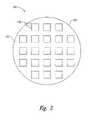
- FIG. 2is a schematic top plan view of a semiconductor workpiece.
- FIG. 3is a schematic side cross-sectional view of a portion of the workpiece of FIG. 2 .
- FIG. 4is a schematic side cross-sectional view of the portion of the semiconductor workpiece after forming an adhesive layer on the stand-off layer.
- FIG. 5is a schematic side cross-sectional view of the portion of the semiconductor workpiece after removing sections of the stand-off and adhesive layers.
- FIG. 6is a schematic side cross-sectional view of the portion of the semiconductor workpiece after inverting the workpiece and reattaching the workpiece to the support member.
- FIG. 7is a schematic side cross-sectional view of a microelectronic device assembly including a lead frame, a microelectronic die attached to the lead frame, and a first singulated microelectronic device attached to the die.
- FIG. 8is a schematic side cross-sectional view of the microelectronic device assembly after attaching a second singulated microelectronic device to the first singulated microelectronic device.
- FIG. 9is a schematic side cross-sectional view of a packaged microelectronic device in accordance with another embodiment of the disclosure.
- FIGS. 10 and 11illustrate stages of a method of manufacturing a packaged microelectronic device in accordance with another embodiment of the disclosure.
- FIG. 10is a schematic side cross-sectional view of a portion of a workpiece including a stand-off structure and first and second adhesive layers formed on the stand-off structure.
- FIG. 11is a schematic side cross-sectional view of a packaged microelectronic device in accordance with another embodiment of the disclosure.
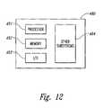
- FIG. 12is a schematic illustration of a system in which the microelectronic devices may be incorporated.
- the packaged microelectronic devicescan have a different number of stacked dies and/or may include other components.
- the microelectronic devicescan include micromechanical components, data storage elements, optics, read/write components, or other features.
- the microelectronic diescan be SRAM, DRAM (e.g., DDR-SDRAM), flash-memory (e.g., NAND flash-memory), processors, imagers, and other types of devices.
- DRAMe.g., DDR-SDRAM
- flash-memorye.g., NAND flash-memory
- processorsimagers
- imagerse.g., imagers, and other types of devices.
- several additional embodiments of the inventioncan have different configurations, components, or procedures than those described in this section. A person of ordinary skill in the art, therefore, will accordingly understand that the invention may have other embodiments with additional elements, or the invention may have other embodiments without several of the elements shown and described below with reference to
- FIGS. 2-8illustrate stages of a method of manufacturing a packaged microelectronic device in accordance with one embodiment of the disclosure.
- FIG. 2is a schematic top plan view of a semiconductor workpiece 100
- FIG. 3is a schematic side cross-sectional view of a portion of the workpiece 100 .
- the illustrated semiconductor workpiece 100is a wafer 101 in and on which devices are constructed.
- the workpiece 100includes a substrate 102 and a plurality of microelectronic dies 110 (only three are shown) formed in and/or on the substrate 102 .
- the individual dies 110include an active side 112 , a backside 114 opposite the active side 112 , a plurality of terminals 116 (e.g., bond-pads) arranged in an array on the active side 112 , and an integrated circuit 118 (shown schematically) operably coupled to the terminals 116 .
- the illustrated dies 110have the same structure, in other embodiments the dies may have different features to perform different functions.
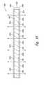
- a stand-off layer 120is formed across the semiconductor workpiece 100 at the backsides 114 of the dies 110 .
- the stand-off layer 120can be formed on the workpiece 100 by molding, spin-on techniques, film lamination, screen printing, spraying, brushing, a dip bath, or other suitable processes.
- the stand-off layer 120has a precise and generally uniform thickness and may be generally incompressible.
- the stand-off layer 120can be approximately 60 microns, but in other embodiments the stand-off layer 120 can have a thickness greater than or less than 60 microns.
- the stand-off layer 120can be made of a generally non-compressible material.
- the stand-off layer 120may be composed of epoxy, epoxy acrylic, polyimide, or other suitable materials.
- FIG. 4is a schematic side cross-sectional view of the portion of the semiconductor workpiece 100 after forming an adhesive layer 140 on the stand-off layer 120 .
- the adhesive layer 140can be a die attach film or other suitable member for connecting the dies 110 to other dies as described below.
- the combination of the stand-off and adhesive layers 120 and 140has a precise thickness T within the range of the desired distance between pairs of stacked microelectronic dies in a packaged microelectronic device as described in greater detail below.
- the workpiece 100may not include the adhesive layer 140 .
- the semiconductor workpiece 100can be removably attached to a support member 190 during several processing procedures to provide support to the workpiece 100 .
- the support member 190may include a dicing support having an annular frame 192 carrying a replaceable film 194 that can include an attachment device 196 (e.g., UV tape) for releasably adhering the support member 190 to the active side 112 of the dies 110 .
- an attachment device 196e.g., UV tape
- FIG. 5is a schematic side cross-sectional view of the portion of the semiconductor workpiece 100 after removing sections of the stand-off and adhesive layers 120 and 140 to form a plurality of discrete stand-offs 130 with adhesive sections 142 on corresponding dies 110 .
- Sections of the stand-off and adhesive layers 120 and 140can be removed via etching, cutting (e.g., with a wafer saw or dicing blade), or other suitable methods.
- the stand-off and/or adhesive layer 120 and/or 140can be composed of a photoactive material, and sections of these layers 120 and/or 140 can be exposed and developed to form the stand-offs 130 .
- the individual stand-offs 130include a first surface 132 facing a corresponding die 110 , a second surface 134 opposite the first surface 132 , and a plurality of ends 136 extending between the first and second surfaces 132 and 134 .
- the first surfaces 132are attached to corresponding dies 110 without an adhesive because the stand-offs 130 themselves adhere to the dies 110 .
- the second surfaces 134are generally planar and oriented parallel to the backsides 114 of the dies 110 .
- the ends 136are spaced apart so that the illustrated stand-offs 130 are positioned inboard the terminals 116 (i.e., between the terminals 116 and the center of the particular die 110 ) and over the central portion of the corresponding dies 110 .
- the stand-offs 130have a rectangular cross-sectional shape and are positioned on the dies 110 in a one-to-one correspondence, in other embodiments the stand-offs can have other cross-sectional shapes and/or a plurality of stand-offs can be formed on each die 110 . In either case, the position of the stand-offs 130 is driven by the configuration of the dies to which the particular stand-offs 130 are attached.
- the individual adhesive sections 142include a first surface 144 facing the second surface 134 of the corresponding stand-off 130 and a second surface 146 opposite the first surface 144 .
- the second surfaces 146are generally planar and oriented parallel to the backsides 114 of the dies 110 .
- FIG. 6is a schematic side cross-sectional view of the portion of the semiconductor workpiece 100 after inverting the workpiece 100 and reattaching the workpiece 100 to the support member 190 with the stand-offs 130 positioned between the dies 110 and the support member 190 .
- the workpiece 100is removably attached to the support member 190 with the second surface 146 of the adhesive sections 142 contacting the attachment device 196 (e.g., UV tape).
- the workpiece 100is then cut along lines A-A to singulate a plurality of microelectronic devices 104 .
- the individual microelectronic devices 104can be removed from the support member 190 via a conventional pick-and-place apparatus.
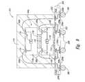
- FIG. 7is a schematic side cross-sectional view of a microelectronic device assembly 103 including a support member or lead frame 150 , a microelectronic die 110 a attached to the lead frame 150 , and a first singulated microelectronic device 104 a attached to the die 110 a .
- the die 110 awill be referred to as a first die 110 a
- the die 110 of the first singulated microelectronic device 104 awill be referred to as a second die 110 b .
- the lead frame 150includes (a) a die paddle 152 for carrying the first die 110 a and the first singulated microelectronic device 104 a , and (b) a plurality of leads 154 (only two are shown) for providing external electrical contacts.
- the first die 110 acan be either generally similar to the second die 110 b or have different features to perform different functions.
- the illustrated first die 110 aincludes an active side 112 , a backside 114 opposite the active side 112 , a plurality of terminals 116 (e.g., bond-pads) arranged in an array on the active side 112 , and an integrated circuit 118 (shown schematically) operably coupled to the terminals 116 .
- the backside 114 of the first die 110 ais attached to the die paddle 152 with an adhesive 148 .
- the terminals 116can be electrically coupled to corresponding leads 154 with a plurality of first wire-bonds 160 a.
- the first singulated microelectronic device 104 acan be attached to the first die 110 a with the stand-off 130 positioned between the first and second dies 110 a and 110 b .
- the second surface 146 of the adhesive section 142is placed against the active side 112 of the first die 110 a such that the first microelectronic device 104 a adheres to the first die 110 a .
- the stand-off 130 and adhesive section 142are positioned inboard the terminals 116 of the first die 110 a so as not to interfere with the first wire-bonds 160 a .
- the combined thickness T of the stand-off 130 and the adhesive section 142is sized to space the first and second dies 110 a - b apart by a sufficient distance so that the first wire-bonds 160 a can electrically couple the first die 110 a to the leads 154 without contacting the second die 110 b .
- the combined thickness T of the stand-off 130 and the adhesive section 142is greater than a distance D that the first wire-bonds 160 a project from the active surface 112 of the first die 110 a .
- FIG. 8is a schematic side cross-sectional view of the microelectronic device assembly 103 after attaching a second singulated microelectronic device 104 b to the first singulated microelectronic device 104 a .
- the second microelectronic device 104 bcan be attached to the first microelectronic device 104 a in generally the same manner as the first microelectronic device 104 a is attached to the first die 110 a .
- the second microelectronic device 104 bis electrically connected to corresponding leads 154 with a plurality of third wire-bonds 160 c .
- the assembly 103may not include the second microelectronic device 104 b or the assembly 103 may include four or more microelectronic devices attached in a stacked configuration. In either case, a casing 170 is formed over the assembly 103 to encapsulate the first die 110 a , the microelectronic devices 104 , the wire-bonds 160 , and a portion of the lead frame 150 . The encased assembly 103 accordingly forms a packaged microelectronic device 103 a.
- the stand-offs 130 and adhesive sections 142can be formed with a precise, uniform thickness T so that the second and third microelectronic dies 110 b - c are oriented generally parallel to the first microelectronic die 110 a .
- the packaged microelectronic device 103 ais expected to not have problems with die tilt and the concomitant exposure and/or shorting of wire-bonds.
- the stand-offs 130can be formed with relatively inexpensive materials, rather than expensive sections of a semiconductor wafer.
- a method of manufacturing a microelectronic deviceincludes forming a stand-off layer over a plurality of microelectronic dies on a semiconductor workpiece, and removing selected portions of the stand-off layer to form a plurality of stand-offs.
- the individual stand-offsare positioned on a backside of a corresponding die.
- the methodfurther includes cutting the semiconductor workpiece to singulate the dies, and attaching the stand-off on a first singulated die to a second die.
- a methodin another embodiment, includes forming a stand-off on a first microelectronic die, attaching a second microelectronic die to a support member, and coupling the stand-off to the second die.
- the stand-offis coupled to the second die after forming the stand-off on the first die and attaching the second die to the support member.
- the methodfurther includes encapsulating the first and second dies and at least a portion of the support member.
- a methodin another embodiment, includes molding a stand-off structure, forming an adhesive layer on the stand-off structure, and cutting the stand-off structure to form a plurality of stand-offs. The method further includes attaching a first microelectronic die to a support member, coupling a first singulated stand-off to the first die, and connecting a second microelectronic die to the first singulated stand-off.
- a systemcomprises a microelectronic device including a support member and a first microelectronic die.
- the first dieincludes a backside attached to the support member, an active side opposite the backside, a plurality of terminals at the active side, and an integrated circuit operably coupled to the terminals.
- the devicefurther includes a stand-off attached to the active side of the first die, and a second microelectronic die attached to the stand-off.
- the second dieincludes a backside, an active side opposite the backside, a plurality of terminals at the active side, and an integrated circuit operably coupled to the terminals.
- the backside of the second dieis attached to the stand-off without an adhesive positioned between the stand-off and the backside of the second die.
- a semiconductor workpiecein another embodiment, includes a substrate having a plurality of microelectronic dies.
- the individual diesinclude an active side, a backside opposite the active side, a plurality of terminals at the active side, and an integrated circuit operably coupled to the terminals.
- the workpiecefurther includes a plurality of stand-offs on the backsides of corresponding dies, and a plurality of adhesive sections attached to corresponding stand-offs.
- a microelectronic devicein another embodiment, includes a microelectronic die, a stand-off coupled to the die, and an exposed adhesive attached to the stand-off.
- the dieincludes an exposed active side, a backside opposite the active side, a plurality of terminals at the active side, and an integrated circuit operably coupled to the terminals.
- the stand-offis positioned at least partially inboard the terminals of the die and includes a first surface attached to the backside of the die and a second surface opposite the first surface.
- the exposed adhesiveis placed on the second surface of the stand-off.
- FIG. 9is a schematic side cross-sectional view of a packaged microelectronic device 203 in accordance with another embodiment of the disclosure.
- the packaged microelectronic device 203is generally similar to the packaged microelectronic device 103 a described above with reference to FIGS. 2-8 .
- the packaged microelectronic device 203includes a first die 110 a and a first microelectronic device 104 a attached to the first die 110 a .
- the illustrated packaged microelectronic device 203does not include a second microelectronic device attached to the first microelectronic device 104 a .
- the support member of the illustrated packaged microelectronic device 203includes an interposer substrate 250 in lieu of a lead frame.
- the interposer substrate 250includes a first side 252 attached to the backside 114 of the first die 110 a and a second side 253 opposite the first side 252 .
- the first side 252includes (a) a plurality of first contacts 254 a arranged in arrays for attachment to corresponding first wire-bonds 160 a , and (b) a plurality of second contacts 254 arranged in arrays for attachment to corresponding second wire-bonds 160 b .
- the second side 253includes (a) a plurality of first pads 256 a electrically connected to corresponding first contacts 254 a with a plurality of first conductive traces 258 a , and (b) a plurality of second pads 256 b electrically connected to corresponding second contacts 254 b with a plurality of second conductive traces 258 b .
- the illustrated packaged microelectronic device 203further includes a plurality of electrical couplers 280 (e.g., solder balls) attached to the first and second pads 256 a - b.
- FIGS. 10 and 11illustrate stages of a method of manufacturing a packaged microelectronic device in accordance with another embodiment of the disclosure.
- FIG. 10is a schematic side cross-sectional view of a portion of a workpiece 300 including a stand-off structure 320 and first and second adhesive layers 340 a - b formed on the stand-off structure 320 .
- the stand-off structure 320has a circular, rectangular, or other suitable planform shape and includes a first major surface 322 and a second major surface 324 opposite the first major surface 322 .
- the stand-off structure 320includes a flowable dielectric material and can be formed via molding or other suitable methods.
- the first adhesive layer 340 ais placed on the first major surface 322 and the second adhesive layer 340 b is placed on the second major surface 324 .
- the workpiece 300is cut along lines B-B to singulate a plurality of individual stand-offs 330 with corresponding adhesive sections 342 a - b .
- the workpiece 300may not include one or both of the adhesive layers 340 such that one or both of the major surfaces 322 and 324 are exposed.
- FIG. 11is a schematic side cross-sectional view of a packaged microelectronic device 303 in accordance with another embodiment of the disclosure.
- the packaged microelectronic device 303is generally similar to the packaged microelectronic device 103 a described above with reference to FIGS. 2-8 .
- the packaged microelectronic device 303includes a lead frame 150 , a first die 110 a attached to the lead frame 150 , and a second die 110 b attached to the first die 110 a .
- the illustrated packaged microelectronic device 303further includes a first singulated stand-off 330 positioned between the first and second dies 110 a - b with the first adhesive section 342 a attached to the active side 112 of the first die 110 a and the second adhesive section 342 b attached to the backside 114 of the second die 110 b .
- the packaged microelectronic device 303may include three or more microelectronic dies 110 attached in a stacked configuration.
- the packaged microelectronic device 303may include an interposer substrate in lieu of the lead frame 150 .
- the system 490can include a processor 491 , a memory 492 (e.g., SRAM, DRAM, Flash, and/or other memory device), input/output devices 493 , and/or other subsystems or components 494 .
- Microelectronic devicesmay be included in any of the components shown in FIG. 12 .
- the resulting system 490can perform any of a wide variety of computing, processing, storage, sensor, imagers, and/or other functions.
- representative systems 490include, without limitation, computers and/or other data processors, for example, desktop computers, laptop computers, Internet appliances, hand-held devices (e.g., palm-top computers, wearable computers, cellular or mobile phones, personal digital assistants), multi-processor systems, processor-based or programmable consumer electronics, network computers, and mini computers.
- Other representative systems 490include cameras, light or other radiation sensors, servers and associated server subsystems, display devices, and/or memory devices.
- individual diescan include imager arrays, such as CMOS imagers.
- Components of the system 490may be housed in a single unit or distributed over multiple, interconnected units, e.g., through a communications network. Components can accordingly include local and/or remote memory storage devices, and any of a wide variety of computer-readable media.
Landscapes
- Engineering & Computer Science (AREA)
- Microelectronics & Electronic Packaging (AREA)
- Power Engineering (AREA)
- Computer Hardware Design (AREA)
- Physics & Mathematics (AREA)
- Condensed Matter Physics & Semiconductors (AREA)
- General Physics & Mathematics (AREA)
- Manufacturing & Machinery (AREA)
- Die Bonding (AREA)
- Container, Conveyance, Adherence, Positioning, Of Wafer (AREA)
- Encapsulation Of And Coatings For Semiconductor Or Solid State Devices (AREA)
- Dicing (AREA)
Abstract
Description
Claims (20)
Priority Applications (3)
| Application Number | Priority Date | Filing Date | Title |
|---|---|---|---|
| US12/792,576US8399971B2 (en) | 2006-12-04 | 2010-06-02 | Packaged microelectronic devices and methods for manufacturing packaged microelectronic devices |
| US13/845,686US8900923B2 (en) | 2006-12-04 | 2013-03-18 | Packaged microelectronic devices and methods for manufacturing packaged microelectronic devices |
| US14/558,184US9324676B2 (en) | 2006-12-04 | 2014-12-02 | Packaged microelectronic devices and methods for manufacturing packaged microelectronic devices |
Applications Claiming Priority (2)
| Application Number | Priority Date | Filing Date | Title |
|---|---|---|---|
| SG200608455-2ASG143098A1 (en) | 2006-12-04 | 2006-12-04 | Packaged microelectronic devices and methods for manufacturing packaged microelectronic devices |
| SG200608455-2 | 2006-12-04 |
Related Child Applications (1)
| Application Number | Title | Priority Date | Filing Date |
|---|---|---|---|
| US12/792,576DivisionUS8399971B2 (en) | 2006-12-04 | 2010-06-02 | Packaged microelectronic devices and methods for manufacturing packaged microelectronic devices |
Publications (2)
| Publication Number | Publication Date |
|---|---|
| US20080128900A1 US20080128900A1 (en) | 2008-06-05 |
| US7741150B2true US7741150B2 (en) | 2010-06-22 |
Family
ID=39474769
Family Applications (4)
| Application Number | Title | Priority Date | Filing Date |
|---|---|---|---|
| US11/626,683Active2027-08-05US7741150B2 (en) | 2006-12-04 | 2007-01-24 | Packaged microelectronic devices and methods for manufacturing packaged microelectronic devices |
| US12/792,576Active2027-10-20US8399971B2 (en) | 2006-12-04 | 2010-06-02 | Packaged microelectronic devices and methods for manufacturing packaged microelectronic devices |
| US13/845,686Active2027-04-07US8900923B2 (en) | 2006-12-04 | 2013-03-18 | Packaged microelectronic devices and methods for manufacturing packaged microelectronic devices |
| US14/558,184ActiveUS9324676B2 (en) | 2006-12-04 | 2014-12-02 | Packaged microelectronic devices and methods for manufacturing packaged microelectronic devices |
Family Applications After (3)
| Application Number | Title | Priority Date | Filing Date |
|---|---|---|---|
| US12/792,576Active2027-10-20US8399971B2 (en) | 2006-12-04 | 2010-06-02 | Packaged microelectronic devices and methods for manufacturing packaged microelectronic devices |
| US13/845,686Active2027-04-07US8900923B2 (en) | 2006-12-04 | 2013-03-18 | Packaged microelectronic devices and methods for manufacturing packaged microelectronic devices |
| US14/558,184ActiveUS9324676B2 (en) | 2006-12-04 | 2014-12-02 | Packaged microelectronic devices and methods for manufacturing packaged microelectronic devices |
Country Status (2)
| Country | Link |
|---|---|
| US (4) | US7741150B2 (en) |
| SG (1) | SG143098A1 (en) |
Cited By (4)
| Publication number | Priority date | Publication date | Assignee | Title |
|---|---|---|---|---|
| US20100244272A1 (en)* | 2008-06-10 | 2010-09-30 | Micron Technology, Inc. | Packaged microelectronic devices and methods for manufacturing packaged microelectronic devices |
| US20100244229A1 (en)* | 2009-03-31 | 2010-09-30 | Stmicroelectronics (Grenoble 2) Sas | Semiconductor package fabrication process and semiconductor package |
| US20110101491A1 (en)* | 2007-09-25 | 2011-05-05 | Oswald Skeete | Integrated circuit packages including high density bump-less build up layers and a lesser density core or coreless substrate |
| US20120280344A1 (en)* | 2011-05-05 | 2012-11-08 | Lightwire LLC | Wafer Scale Packaging Platform For Transceivers |
Families Citing this family (19)
| Publication number | Priority date | Publication date | Assignee | Title |
|---|---|---|---|---|
| US20070045807A1 (en)* | 2005-09-01 | 2007-03-01 | Micron Technology, Inc. | Microelectronic devices and methods for manufacturing microelectronic devices |
| SG143098A1 (en) | 2006-12-04 | 2008-06-27 | Micron Technology Inc | Packaged microelectronic devices and methods for manufacturing packaged microelectronic devices |
| US9466719B2 (en) | 2009-07-15 | 2016-10-11 | Qualcomm Incorporated | Semiconductor-on-insulator with back side strain topology |
| US9390974B2 (en) | 2012-12-21 | 2016-07-12 | Qualcomm Incorporated | Back-to-back stacked integrated circuit assembly and method of making |
| US9034732B2 (en)* | 2009-07-15 | 2015-05-19 | Silanna Semiconductor U.S.A., Inc. | Semiconductor-on-insulator with back side support layer |
| US9496227B2 (en) | 2009-07-15 | 2016-11-15 | Qualcomm Incorporated | Semiconductor-on-insulator with back side support layer |
| US8921168B2 (en) | 2009-07-15 | 2014-12-30 | Silanna Semiconductor U.S.A., Inc. | Thin integrated circuit chip-on-board assembly and method of making |
| KR101818556B1 (en) | 2009-07-15 | 2018-01-15 | 퀄컴 인코포레이티드 | Semiconductor-on-insulator with back side body connection |
| KR101758852B1 (en)* | 2009-07-15 | 2017-07-17 | 퀄컴 인코포레이티드 | Semiconductor-on-insulator with backside heat dissipation |
| US8564141B2 (en)* | 2010-05-06 | 2013-10-22 | SK Hynix Inc. | Chip unit and stack package having the same |
| US8686547B1 (en)* | 2011-01-03 | 2014-04-01 | Marvell International Ltd. | Stack die structure for stress reduction and facilitation of electromagnetic shielding |
| US9147628B2 (en)* | 2012-06-27 | 2015-09-29 | Infineon Technoloiges Austria AG | Package-in-packages and methods of formation thereof |
| US9515181B2 (en) | 2014-08-06 | 2016-12-06 | Qualcomm Incorporated | Semiconductor device with self-aligned back side features |
| TWI611577B (en)* | 2016-03-04 | 2018-01-11 | 矽品精密工業股份有限公司 | Electronic package and semiconductor substrate |
| US9917041B1 (en)* | 2016-10-28 | 2018-03-13 | Intel Corporation | 3D chip assemblies using stacked leadframes |
| US10193011B1 (en)* | 2017-07-14 | 2019-01-29 | Globalfoundries Inc. | Method of manufacturing a 3 color LED integrated Si CMOS driver wafer using die to wafer bonding approach |
| WO2019180854A1 (en)* | 2018-03-20 | 2019-09-26 | 株式会社 東芝 | Multi-junction solar cell module and solar power generation system |
| GB2575038B (en)* | 2018-06-25 | 2023-04-19 | Lumentum Tech Uk Limited | A Semiconductor Separation Device |
| WO2020107447A1 (en)* | 2018-11-30 | 2020-06-04 | 北京比特大陆科技有限公司 | Method for manufacturing chip and chip structure |
Citations (58)
| Publication number | Priority date | Publication date | Assignee | Title |
|---|---|---|---|---|
| US5128831A (en) | 1991-10-31 | 1992-07-07 | Micron Technology, Inc. | High-density electronic package comprising stacked sub-modules which are electrically interconnected by solder-filled vias |
| US5252857A (en) | 1991-08-05 | 1993-10-12 | International Business Machines Corporation | Stacked DCA memory chips |
| US5323060A (en) | 1993-06-02 | 1994-06-21 | Micron Semiconductor, Inc. | Multichip module having a stacked chip arrangement |
| US5518957A (en) | 1991-10-10 | 1996-05-21 | Samsung Electronics Co., Ltd. | Method for making a thin profile semiconductor package |
| US5851845A (en) | 1995-12-18 | 1998-12-22 | Micron Technology, Inc. | Process for packaging a semiconductor die using dicing and testing |
| US5883426A (en) | 1996-04-18 | 1999-03-16 | Nec Corporation | Stack module |
| US5933713A (en) | 1998-04-06 | 1999-08-03 | Micron Technology, Inc. | Method of forming overmolded chip scale package and resulting product |
| US5946553A (en) | 1991-06-04 | 1999-08-31 | Micron Technology, Inc. | Process for manufacturing a semiconductor package with bi-substrate die |
| US5986209A (en) | 1997-07-09 | 1999-11-16 | Micron Technology, Inc. | Package stack via bottom leaded plastic (BLP) packaging |
| US5990566A (en) | 1998-05-20 | 1999-11-23 | Micron Technology, Inc. | High density semiconductor package |
| US6004867A (en) | 1996-12-16 | 1999-12-21 | Samsung Electronics Co., Ltd. | Chip-size packages assembled using mass production techniques at the wafer-level |
| US6008070A (en) | 1998-05-21 | 1999-12-28 | Micron Technology, Inc. | Wafer level fabrication and assembly of chip scale packages |
| US6020629A (en) | 1998-06-05 | 2000-02-01 | Micron Technology, Inc. | Stacked semiconductor package and method of fabrication |
| US6028365A (en) | 1998-03-30 | 2000-02-22 | Micron Technology, Inc. | Integrated circuit package and method of fabrication |
| US6051878A (en) | 1997-03-10 | 2000-04-18 | Micron Technology, Inc. | Method of constructing stacked packages |
| US6072233A (en) | 1998-05-04 | 2000-06-06 | Micron Technology, Inc. | Stackable ball grid array package |
| US6072236A (en) | 1996-03-07 | 2000-06-06 | Micron Technology, Inc. | Micromachined chip scale package |
| US6175149B1 (en) | 1998-02-13 | 2001-01-16 | Micron Technology, Inc. | Mounting multiple semiconductor dies in a package |
| US6184465B1 (en) | 1998-11-12 | 2001-02-06 | Micron Technology, Inc. | Semiconductor package |
| US6187615B1 (en) | 1998-08-28 | 2001-02-13 | Samsung Electronics Co., Ltd. | Chip scale packages and methods for manufacturing the chip scale packages at wafer level |
| US6212767B1 (en) | 1999-08-31 | 2001-04-10 | Micron Technology, Inc. | Assembling a stacked die package |
| US6225689B1 (en) | 1998-08-21 | 2001-05-01 | Micron Technology, Inc. | Low profile multi-IC chip package connector |
| US6228687B1 (en) | 1999-06-28 | 2001-05-08 | Micron Technology, Inc. | Wafer-level package and methods of fabricating |
| US6235554B1 (en) | 1995-11-27 | 2001-05-22 | Micron Technology, Inc. | Method for fabricating stackable chip scale semiconductor package |
| US6235552B1 (en) | 1999-07-09 | 2001-05-22 | Samsung Electronics Co., Ltd. | Chip scale package and method for manufacturing the same using a redistribution substrate |
| US6281577B1 (en) | 1996-06-28 | 2001-08-28 | Pac Tech-Packaging Technologies Gmbh | Chips arranged in plurality of planes and electrically connected to one another |
| US6294839B1 (en) | 1999-08-30 | 2001-09-25 | Micron Technology, Inc. | Apparatus and methods of packaging and testing die |
| US6297547B1 (en) | 1998-02-13 | 2001-10-02 | Micron Technology Inc. | Mounting multiple semiconductor dies in a package |
| US6303981B1 (en) | 1999-09-01 | 2001-10-16 | Micron Technology, Inc. | Semiconductor package having stacked dice and leadframes and method of fabrication |
| US6326698B1 (en) | 2000-06-08 | 2001-12-04 | Micron Technology, Inc. | Semiconductor devices having protective layers thereon through which contact pads are exposed and stereolithographic methods of fabricating such semiconductor devices |
| US6326700B1 (en) | 2000-08-15 | 2001-12-04 | United Test Center, Inc. | Low profile semiconductor package and process for making the same |
| US6407381B1 (en) | 2000-07-05 | 2002-06-18 | Amkor Technology, Inc. | Wafer scale image sensor package |
| US6429528B1 (en) | 1998-02-27 | 2002-08-06 | Micron Technology, Inc. | Multichip semiconductor package |
| US6459163B1 (en) | 2001-03-21 | 2002-10-01 | United Test Center, Inc. | Semiconductor device and method for fabricating the same |
| US6503780B1 (en) | 2000-07-05 | 2003-01-07 | Amkor Technology, Inc. | Wafer scale image sensor package fabrication method |
| US20030022462A1 (en) | 2000-06-08 | 2003-01-30 | Farnworth Warren M. | Stereolithographic method and apparatus for fabricating spacers for semiconductor devices and resulting structures |
| US20030038355A1 (en)* | 2001-08-24 | 2003-02-27 | Derderian James M. | Semiconductor devices and semiconductor device assemblies including a nonconfluent spacer layer |
| US6531784B1 (en) | 2000-06-02 | 2003-03-11 | Amkor Technology, Inc. | Semiconductor package with spacer strips |
| US6548376B2 (en) | 2001-08-30 | 2003-04-15 | Micron Technology, Inc. | Methods of thinning microelectronic workpieces |
| US6552910B1 (en) | 2000-06-28 | 2003-04-22 | Micron Technology, Inc. | Stacked-die assemblies with a plurality of microelectronic devices and methods of manufacture |
| US6560117B2 (en) | 2000-06-28 | 2003-05-06 | Micron Technology, Inc. | Packaged microelectronic die assemblies and methods of manufacture |
| US6576531B2 (en) | 2001-08-24 | 2003-06-10 | Micron Technology, Inc. | Method for cutting semiconductor wafers |
| US6607937B1 (en) | 2000-08-23 | 2003-08-19 | Micron Technology, Inc. | Stacked microelectronic dies and methods for stacking microelectronic dies |
| US20040038447A1 (en) | 2002-08-21 | 2004-02-26 | Corisis David J | Packaged microelectronic devices and methods for assembling microelectronic devices |
| US6753613B2 (en) | 2002-03-13 | 2004-06-22 | Intel Corporation | Stacked dice standoffs |
| US20040163240A1 (en) | 2002-12-24 | 2004-08-26 | Stmicroelectronics S.R.L. | Manufacturing process of a stacked semiconductor device and corresponding device |
| US20050023655A1 (en) | 2001-08-29 | 2005-02-03 | Fee Setho Sing | Packaged microelectronic devices and methods of forming same |
| US20050212109A1 (en)* | 2004-03-23 | 2005-09-29 | Cherukuri Kalyan C | Vertically stacked semiconductor device |
| US20060022323A1 (en)* | 2004-07-29 | 2006-02-02 | Swee Seng Eric T | Assemblies including stacked semiconductor dice having centrally located, wire bonded bond pads |
| US20060043509A1 (en) | 2004-08-24 | 2006-03-02 | Watkins Charles M | Packaged microelectronic imaging devices and methods of packaging microelectronic imaging devices |
| US20060180907A1 (en) | 2000-08-24 | 2006-08-17 | Micron Technology, Inc. | Packaged microelectronic devices with pressure release elements and methods for manufacturing and using such packaged microelectonic devices |
| US20070045807A1 (en)* | 2005-09-01 | 2007-03-01 | Micron Technology, Inc. | Microelectronic devices and methods for manufacturing microelectronic devices |
| US20070045796A1 (en)* | 2005-08-19 | 2007-03-01 | Micron Technology, Inc. | Microelectronic devices, stacked microelectronic devices, and methods for manufacturing microelectronic devices |
| US20070178666A1 (en)* | 2006-01-31 | 2007-08-02 | Stats Chippac Ltd. | Integrated circuit system with waferscale spacer system |
| US20070289777A1 (en)* | 2006-06-14 | 2007-12-20 | Stats Chippac Ltd. | Package-on-package system |
| US20080042245A1 (en)* | 2006-08-18 | 2008-02-21 | Stats Chippac Ltd. | Integrated circuit package system with waferscale spacer |
| US20080128900A1 (en)* | 2006-12-04 | 2008-06-05 | Micron Technology, Inc. | Packaged microelectronic devices and methods for manufacturing packaged microelectronic devices |
| US20080237824A1 (en)* | 2006-02-17 | 2008-10-02 | Amkor Technology, Inc. | Stacked electronic component package having single-sided film spacer |
Family Cites Families (17)
| Publication number | Priority date | Publication date | Assignee | Title |
|---|---|---|---|---|
| US6005778A (en)* | 1995-06-15 | 1999-12-21 | Honeywell Inc. | Chip stacking and capacitor mounting arrangement including spacers |
| JP3544895B2 (en) | 1999-07-30 | 2004-07-21 | シャープ株式会社 | Resin-sealed semiconductor device and method of manufacturing the same |
| US6549376B1 (en)* | 2000-03-31 | 2003-04-15 | John E. Scura | Gimbal suspension with vibration damper |
| US6503776B2 (en) | 2001-01-05 | 2003-01-07 | Advanced Semiconductor Engineering, Inc. | Method for fabricating stacked chip package |
| US20030111720A1 (en)* | 2001-12-18 | 2003-06-19 | Tan Lan Chu | Stacked die semiconductor device |
| CN1251318C (en) | 2002-02-25 | 2006-04-12 | 精工爱普生株式会社 | Semiconductor water, semiconductor device and their producing method, circuit board and instrument |
| US6703075B1 (en) | 2002-12-24 | 2004-03-09 | Chipmos Technologies (Bermuda) Ltd. | Wafer treating method for making adhesive dies |
| US7713841B2 (en) | 2003-09-19 | 2010-05-11 | Micron Technology, Inc. | Methods for thinning semiconductor substrates that employ support structures formed on the substrates |
| US20050112842A1 (en) | 2003-11-24 | 2005-05-26 | Kang Jung S. | Integrating passive components on spacer in stacked dies |
| US7422930B2 (en) | 2004-03-02 | 2008-09-09 | Infineon Technologies Ag | Integrated circuit with re-route layer and stacked die assembly |
| US7492039B2 (en)* | 2004-08-19 | 2009-02-17 | Micron Technology, Inc. | Assemblies and multi-chip modules including stacked semiconductor dice having centrally located, wire bonded bond pads |
| TWI292224B (en)* | 2005-09-02 | 2008-01-01 | Advanced Semiconductor Eng | Multi-chip package structure |
| US20070152314A1 (en)* | 2005-12-30 | 2007-07-05 | Intel Corporation | Low stress stacked die packages |
| US20070231970A1 (en)* | 2006-03-31 | 2007-10-04 | Tsuyoshi Fukuo | Cured mold compound spacer for stacked-die package |
| US20080054429A1 (en) | 2006-08-25 | 2008-03-06 | Bolken Todd O | Spacers for separating components of semiconductor device assemblies, semiconductor device assemblies and systems including spacers and methods of making spacers |
| US8198713B2 (en)* | 2007-07-13 | 2012-06-12 | Infineon Technologies Ag | Semiconductor wafer structure |
| SG150395A1 (en)* | 2007-08-16 | 2009-03-30 | Micron Technology Inc | Stacked microelectronic devices and methods for manufacturing stacked microelectronic devices |
- 2006
- 2006-12-04SGSG200608455-2Apatent/SG143098A1/enunknown
- 2007
- 2007-01-24USUS11/626,683patent/US7741150B2/enactiveActive
- 2010
- 2010-06-02USUS12/792,576patent/US8399971B2/enactiveActive
- 2013
- 2013-03-18USUS13/845,686patent/US8900923B2/enactiveActive
- 2014
- 2014-12-02USUS14/558,184patent/US9324676B2/enactiveActive
Patent Citations (65)
| Publication number | Priority date | Publication date | Assignee | Title |
|---|---|---|---|---|
| US6020624A (en) | 1991-06-04 | 2000-02-01 | Micron Technology, Inc. | Semiconductor package with bi-substrate die |
| US5946553A (en) | 1991-06-04 | 1999-08-31 | Micron Technology, Inc. | Process for manufacturing a semiconductor package with bi-substrate die |
| US5252857A (en) | 1991-08-05 | 1993-10-12 | International Business Machines Corporation | Stacked DCA memory chips |
| US5518957A (en) | 1991-10-10 | 1996-05-21 | Samsung Electronics Co., Ltd. | Method for making a thin profile semiconductor package |
| US5128831A (en) | 1991-10-31 | 1992-07-07 | Micron Technology, Inc. | High-density electronic package comprising stacked sub-modules which are electrically interconnected by solder-filled vias |
| US5323060A (en) | 1993-06-02 | 1994-06-21 | Micron Semiconductor, Inc. | Multichip module having a stacked chip arrangement |
| US6235554B1 (en) | 1995-11-27 | 2001-05-22 | Micron Technology, Inc. | Method for fabricating stackable chip scale semiconductor package |
| US5851845A (en) | 1995-12-18 | 1998-12-22 | Micron Technology, Inc. | Process for packaging a semiconductor die using dicing and testing |
| US6124634A (en) | 1996-03-07 | 2000-09-26 | Micron Technology, Inc. | Micromachined chip scale package |
| US6072236A (en) | 1996-03-07 | 2000-06-06 | Micron Technology, Inc. | Micromachined chip scale package |
| US5883426A (en) | 1996-04-18 | 1999-03-16 | Nec Corporation | Stack module |
| US6281577B1 (en) | 1996-06-28 | 2001-08-28 | Pac Tech-Packaging Technologies Gmbh | Chips arranged in plurality of planes and electrically connected to one another |
| US6004867A (en) | 1996-12-16 | 1999-12-21 | Samsung Electronics Co., Ltd. | Chip-size packages assembled using mass production techniques at the wafer-level |
| US6051878A (en) | 1997-03-10 | 2000-04-18 | Micron Technology, Inc. | Method of constructing stacked packages |
| US5986209A (en) | 1997-07-09 | 1999-11-16 | Micron Technology, Inc. | Package stack via bottom leaded plastic (BLP) packaging |
| US6297547B1 (en) | 1998-02-13 | 2001-10-02 | Micron Technology Inc. | Mounting multiple semiconductor dies in a package |
| US6175149B1 (en) | 1998-02-13 | 2001-01-16 | Micron Technology, Inc. | Mounting multiple semiconductor dies in a package |
| US6429528B1 (en) | 1998-02-27 | 2002-08-06 | Micron Technology, Inc. | Multichip semiconductor package |
| US6028365A (en) | 1998-03-30 | 2000-02-22 | Micron Technology, Inc. | Integrated circuit package and method of fabrication |
| US5933713A (en) | 1998-04-06 | 1999-08-03 | Micron Technology, Inc. | Method of forming overmolded chip scale package and resulting product |
| US6072233A (en) | 1998-05-04 | 2000-06-06 | Micron Technology, Inc. | Stackable ball grid array package |
| US5990566A (en) | 1998-05-20 | 1999-11-23 | Micron Technology, Inc. | High density semiconductor package |
| US6326697B1 (en) | 1998-05-21 | 2001-12-04 | Micron Technology, Inc. | Hermetically sealed chip scale packages formed by wafer level fabrication and assembly |
| US6008070A (en) | 1998-05-21 | 1999-12-28 | Micron Technology, Inc. | Wafer level fabrication and assembly of chip scale packages |
| US6020629A (en) | 1998-06-05 | 2000-02-01 | Micron Technology, Inc. | Stacked semiconductor package and method of fabrication |
| US6225689B1 (en) | 1998-08-21 | 2001-05-01 | Micron Technology, Inc. | Low profile multi-IC chip package connector |
| US6258623B1 (en) | 1998-08-21 | 2001-07-10 | Micron Technology, Inc. | Low profile multi-IC chip package connector |
| US6187615B1 (en) | 1998-08-28 | 2001-02-13 | Samsung Electronics Co., Ltd. | Chip scale packages and methods for manufacturing the chip scale packages at wafer level |
| US6184465B1 (en) | 1998-11-12 | 2001-02-06 | Micron Technology, Inc. | Semiconductor package |
| US6228687B1 (en) | 1999-06-28 | 2001-05-08 | Micron Technology, Inc. | Wafer-level package and methods of fabricating |
| US6235552B1 (en) | 1999-07-09 | 2001-05-22 | Samsung Electronics Co., Ltd. | Chip scale package and method for manufacturing the same using a redistribution substrate |
| US6294839B1 (en) | 1999-08-30 | 2001-09-25 | Micron Technology, Inc. | Apparatus and methods of packaging and testing die |
| US6212767B1 (en) | 1999-08-31 | 2001-04-10 | Micron Technology, Inc. | Assembling a stacked die package |
| US6303981B1 (en) | 1999-09-01 | 2001-10-16 | Micron Technology, Inc. | Semiconductor package having stacked dice and leadframes and method of fabrication |
| US6531784B1 (en) | 2000-06-02 | 2003-03-11 | Amkor Technology, Inc. | Semiconductor package with spacer strips |
| US20030032217A1 (en) | 2000-06-08 | 2003-02-13 | Farnworth Warren M. | Stereolithographic method and apparatus for fabricating spacers for semiconductor devices and resulting structures |
| US6326698B1 (en) | 2000-06-08 | 2001-12-04 | Micron Technology, Inc. | Semiconductor devices having protective layers thereon through which contact pads are exposed and stereolithographic methods of fabricating such semiconductor devices |
| US20030022462A1 (en) | 2000-06-08 | 2003-01-30 | Farnworth Warren M. | Stereolithographic method and apparatus for fabricating spacers for semiconductor devices and resulting structures |
| US6560117B2 (en) | 2000-06-28 | 2003-05-06 | Micron Technology, Inc. | Packaged microelectronic die assemblies and methods of manufacture |
| US6552910B1 (en) | 2000-06-28 | 2003-04-22 | Micron Technology, Inc. | Stacked-die assemblies with a plurality of microelectronic devices and methods of manufacture |
| US6503780B1 (en) | 2000-07-05 | 2003-01-07 | Amkor Technology, Inc. | Wafer scale image sensor package fabrication method |
| US6407381B1 (en) | 2000-07-05 | 2002-06-18 | Amkor Technology, Inc. | Wafer scale image sensor package |
| US6326700B1 (en) | 2000-08-15 | 2001-12-04 | United Test Center, Inc. | Low profile semiconductor package and process for making the same |
| US6607937B1 (en) | 2000-08-23 | 2003-08-19 | Micron Technology, Inc. | Stacked microelectronic dies and methods for stacking microelectronic dies |
| US20060180907A1 (en) | 2000-08-24 | 2006-08-17 | Micron Technology, Inc. | Packaged microelectronic devices with pressure release elements and methods for manufacturing and using such packaged microelectonic devices |
| US6459163B1 (en) | 2001-03-21 | 2002-10-01 | United Test Center, Inc. | Semiconductor device and method for fabricating the same |
| US6790712B2 (en) | 2001-03-21 | 2004-09-14 | United Test Center, Inc. | Semiconductor device and method for fabricating the same |
| US20030038355A1 (en)* | 2001-08-24 | 2003-02-27 | Derderian James M. | Semiconductor devices and semiconductor device assemblies including a nonconfluent spacer layer |
| US6576531B2 (en) | 2001-08-24 | 2003-06-10 | Micron Technology, Inc. | Method for cutting semiconductor wafers |
| US20050023655A1 (en) | 2001-08-29 | 2005-02-03 | Fee Setho Sing | Packaged microelectronic devices and methods of forming same |
| US6548376B2 (en) | 2001-08-30 | 2003-04-15 | Micron Technology, Inc. | Methods of thinning microelectronic workpieces |
| US6753613B2 (en) | 2002-03-13 | 2004-06-22 | Intel Corporation | Stacked dice standoffs |
| US20040038447A1 (en) | 2002-08-21 | 2004-02-26 | Corisis David J | Packaged microelectronic devices and methods for assembling microelectronic devices |
| US20040163240A1 (en) | 2002-12-24 | 2004-08-26 | Stmicroelectronics S.R.L. | Manufacturing process of a stacked semiconductor device and corresponding device |
| US20050212109A1 (en)* | 2004-03-23 | 2005-09-29 | Cherukuri Kalyan C | Vertically stacked semiconductor device |
| US20060022323A1 (en)* | 2004-07-29 | 2006-02-02 | Swee Seng Eric T | Assemblies including stacked semiconductor dice having centrally located, wire bonded bond pads |
| US7276790B2 (en) | 2004-07-29 | 2007-10-02 | Micron Technology, Inc. | Methods of forming a multi-chip module having discrete spacers |
| US20060043509A1 (en) | 2004-08-24 | 2006-03-02 | Watkins Charles M | Packaged microelectronic imaging devices and methods of packaging microelectronic imaging devices |
| US20070045796A1 (en)* | 2005-08-19 | 2007-03-01 | Micron Technology, Inc. | Microelectronic devices, stacked microelectronic devices, and methods for manufacturing microelectronic devices |
| US20070045807A1 (en)* | 2005-09-01 | 2007-03-01 | Micron Technology, Inc. | Microelectronic devices and methods for manufacturing microelectronic devices |
| US20070178666A1 (en)* | 2006-01-31 | 2007-08-02 | Stats Chippac Ltd. | Integrated circuit system with waferscale spacer system |
| US20080237824A1 (en)* | 2006-02-17 | 2008-10-02 | Amkor Technology, Inc. | Stacked electronic component package having single-sided film spacer |
| US20070289777A1 (en)* | 2006-06-14 | 2007-12-20 | Stats Chippac Ltd. | Package-on-package system |
| US20080042245A1 (en)* | 2006-08-18 | 2008-02-21 | Stats Chippac Ltd. | Integrated circuit package system with waferscale spacer |
| US20080128900A1 (en)* | 2006-12-04 | 2008-06-05 | Micron Technology, Inc. | Packaged microelectronic devices and methods for manufacturing packaged microelectronic devices |
Non-Patent Citations (7)
| Title |
|---|
| Office Action issued Dec. 5, 2008 in U.S. Appl. No. 11/217,886. |
| Office Action issued Jun. 9, 2008 in U.S. Appl. No. 11/217,886. |
| Search Report and Examination Report issued Dec. 11, 2008 in Singapore Application No. 200608455-2. |
| U.S. Appl. No. 11/217,886, filed Sep. 1, 2005, Greenwood et al. |
| U.S. Appl. No. 11/509,119, filed Aug. 24, 2006, Bolken et al. |
| Wolf et al., Silicon Processing for the VLSI Era; vol. 1-Process Technology, Lattice Press, 2000, p. 512. |
| Wolf et al., Silicon Processing for the VLSI Era; vol. 1—Process Technology, Lattice Press, 2000, p. 512. |
Cited By (12)
| Publication number | Priority date | Publication date | Assignee | Title |
|---|---|---|---|---|
| US20110101491A1 (en)* | 2007-09-25 | 2011-05-05 | Oswald Skeete | Integrated circuit packages including high density bump-less build up layers and a lesser density core or coreless substrate |
| US9941245B2 (en)* | 2007-09-25 | 2018-04-10 | Intel Corporation | Integrated circuit packages including high density bump-less build up layers and a lesser density core or coreless substrate |
| US20100244272A1 (en)* | 2008-06-10 | 2010-09-30 | Micron Technology, Inc. | Packaged microelectronic devices and methods for manufacturing packaged microelectronic devices |
| US8148807B2 (en)* | 2008-06-10 | 2012-04-03 | Micron Technology, Inc. | Packaged microelectronic devices and associated systems |
| US8940581B2 (en) | 2008-06-10 | 2015-01-27 | Micron Technology, Inc. | Packaged microelectronic devices and methods for manufacturing packaged microelectronic devices |
| US9530748B2 (en) | 2008-06-10 | 2016-12-27 | Micron Technology, Inc. | Packaged microelectronic devices and methods for manufacturing packaged microelectronic devices |
| US10008468B2 (en) | 2008-06-10 | 2018-06-26 | Micron Technology, Inc. | Packaged microelectronic devices and methods for manufacturing packaged microelectronic devices |
| US20100244229A1 (en)* | 2009-03-31 | 2010-09-30 | Stmicroelectronics (Grenoble 2) Sas | Semiconductor package fabrication process and semiconductor package |
| US8372694B2 (en)* | 2009-03-31 | 2013-02-12 | Stmicroelectronics (Grenoble 2) Sas | Semiconductor package fabrication process and semiconductor package |
| US20120280344A1 (en)* | 2011-05-05 | 2012-11-08 | Lightwire LLC | Wafer Scale Packaging Platform For Transceivers |
| US8803269B2 (en)* | 2011-05-05 | 2014-08-12 | Cisco Technology, Inc. | Wafer scale packaging platform for transceivers |
| US9343450B2 (en) | 2011-05-05 | 2016-05-17 | Cisco Technology, Inc. | Wafer scale packaging platform for transceivers |
Also Published As
| Publication number | Publication date |
|---|---|
| US8399971B2 (en) | 2013-03-19 |
| US8900923B2 (en) | 2014-12-02 |
| US20100237510A1 (en) | 2010-09-23 |
| US20080128900A1 (en) | 2008-06-05 |
| US20150130035A1 (en) | 2015-05-14 |
| US20130217182A1 (en) | 2013-08-22 |
| US9324676B2 (en) | 2016-04-26 |
| SG143098A1 (en) | 2008-06-27 |
Similar Documents
| Publication | Publication Date | Title |
|---|---|---|
| US7741150B2 (en) | Packaged microelectronic devices and methods for manufacturing packaged microelectronic devices | |
| CN113130434B (en) | Package structure and manufacturing method thereof | |
| EP2130224B1 (en) | Apparatus for packaging semiconductor devices | |
| US7947529B2 (en) | Microelectronic die packages with leadframes, including leadframe-based interposer for stacked die packages, and associated systems and methods | |
| JP5453692B2 (en) | Microelectronic die package with metal leads, and related systems and methods, including metal leads for stacked die packages | |
| US7560857B2 (en) | Package structure of MEMS microphone | |
| KR101485972B1 (en) | Integrated circuit package system with offset stacked die | |
| US8923004B2 (en) | Microelectronic packages with small footprints and associated methods of manufacturing | |
| TWI463635B (en) | Microelectronic package with stacked microelectronic units and method for manufacture thereof | |
| US20110031614A1 (en) | Methods for fabricating semiconductor components and packaged semiconductor components | |
| JP2009508324A6 (en) | Microelectronic device, stacked microelectronic device, and method of manufacturing microelectronic device | |
| JP2009508324A (en) | Microelectronic device, stacked microelectronic device, and method of manufacturing microelectronic device | |
| KR20110128748A (en) | Integrated circuit packaging system with double side connections and manufacturing method thereof | |
| CN101681886A (en) | Semiconductor assembly, stacked semiconductor device, and methods of manufacturing semiconductor assembly and stacked semiconductor device | |
| CN101627471A (en) | Microelectronic workpieces and methods for manufacturing microelectronic devices using such workpieces | |
| US20160031707A1 (en) | Microelectronic devices and methods for manufacturing microelectronic devices | |
| US9153526B2 (en) | Microelectronic devices and methods for manufacturing microelectronic devices | |
| TW200937540A (en) | Integrated circuit package system with package integration | |
| US8945987B2 (en) | Manufacture of face-down microelectronic packages |
Legal Events
| Date | Code | Title | Description |
|---|---|---|---|
| AS | Assignment | Owner name:MICRON TECHNOLOGY, INC., IDAHO Free format text:ASSIGNMENT OF ASSIGNORS INTEREST;ASSIGNORS:LEOW, SEE HIONG;TAY, LIANG CHEE;REEL/FRAME:019153/0853 Effective date:20070124 Owner name:MICRON TECHNOLOGY, INC.,IDAHO Free format text:ASSIGNMENT OF ASSIGNORS INTEREST;ASSIGNORS:LEOW, SEE HIONG;TAY, LIANG CHEE;REEL/FRAME:019153/0853 Effective date:20070124 | |
| FEPP | Fee payment procedure | Free format text:PAYOR NUMBER ASSIGNED (ORIGINAL EVENT CODE: ASPN); ENTITY STATUS OF PATENT OWNER: LARGE ENTITY | |
| STCF | Information on status: patent grant | Free format text:PATENTED CASE | |
| FPAY | Fee payment | Year of fee payment:4 | |
| AS | Assignment | Owner name:U.S. BANK NATIONAL ASSOCIATION, AS COLLATERAL AGENT, CALIFORNIA Free format text:SECURITY INTEREST;ASSIGNOR:MICRON TECHNOLOGY, INC.;REEL/FRAME:038669/0001 Effective date:20160426 Owner name:U.S. BANK NATIONAL ASSOCIATION, AS COLLATERAL AGEN Free format text:SECURITY INTEREST;ASSIGNOR:MICRON TECHNOLOGY, INC.;REEL/FRAME:038669/0001 Effective date:20160426 | |
| AS | Assignment | Owner name:MORGAN STANLEY SENIOR FUNDING, INC., AS COLLATERAL AGENT, MARYLAND Free format text:PATENT SECURITY AGREEMENT;ASSIGNOR:MICRON TECHNOLOGY, INC.;REEL/FRAME:038954/0001 Effective date:20160426 Owner name:MORGAN STANLEY SENIOR FUNDING, INC., AS COLLATERAL Free format text:PATENT SECURITY AGREEMENT;ASSIGNOR:MICRON TECHNOLOGY, INC.;REEL/FRAME:038954/0001 Effective date:20160426 | |
| AS | Assignment | Owner name:U.S. BANK NATIONAL ASSOCIATION, AS COLLATERAL AGENT, CALIFORNIA Free format text:CORRECTIVE ASSIGNMENT TO CORRECT THE REPLACE ERRONEOUSLY FILED PATENT #7358718 WITH THE CORRECT PATENT #7358178 PREVIOUSLY RECORDED ON REEL 038669 FRAME 0001. ASSIGNOR(S) HEREBY CONFIRMS THE SECURITY INTEREST;ASSIGNOR:MICRON TECHNOLOGY, INC.;REEL/FRAME:043079/0001 Effective date:20160426 Owner name:U.S. BANK NATIONAL ASSOCIATION, AS COLLATERAL AGEN Free format text:CORRECTIVE ASSIGNMENT TO CORRECT THE REPLACE ERRONEOUSLY FILED PATENT #7358718 WITH THE CORRECT PATENT #7358178 PREVIOUSLY RECORDED ON REEL 038669 FRAME 0001. ASSIGNOR(S) HEREBY CONFIRMS THE SECURITY INTEREST;ASSIGNOR:MICRON TECHNOLOGY, INC.;REEL/FRAME:043079/0001 Effective date:20160426 | |
| MAFP | Maintenance fee payment | Free format text:PAYMENT OF MAINTENANCE FEE, 8TH YEAR, LARGE ENTITY (ORIGINAL EVENT CODE: M1552) Year of fee payment:8 | |
| AS | Assignment | Owner name:JPMORGAN CHASE BANK, N.A., AS COLLATERAL AGENT, ILLINOIS Free format text:SECURITY INTEREST;ASSIGNORS:MICRON TECHNOLOGY, INC.;MICRON SEMICONDUCTOR PRODUCTS, INC.;REEL/FRAME:047540/0001 Effective date:20180703 Owner name:JPMORGAN CHASE BANK, N.A., AS COLLATERAL AGENT, IL Free format text:SECURITY INTEREST;ASSIGNORS:MICRON TECHNOLOGY, INC.;MICRON SEMICONDUCTOR PRODUCTS, INC.;REEL/FRAME:047540/0001 Effective date:20180703 | |
| AS | Assignment | Owner name:MICRON TECHNOLOGY, INC., IDAHO Free format text:RELEASE BY SECURED PARTY;ASSIGNOR:U.S. BANK NATIONAL ASSOCIATION, AS COLLATERAL AGENT;REEL/FRAME:047243/0001 Effective date:20180629 | |
| AS | Assignment | Owner name:MICRON TECHNOLOGY, INC., IDAHO Free format text:RELEASE BY SECURED PARTY;ASSIGNOR:MORGAN STANLEY SENIOR FUNDING, INC., AS COLLATERAL AGENT;REEL/FRAME:050937/0001 Effective date:20190731 | |
| AS | Assignment | Owner name:MICRON TECHNOLOGY, INC., IDAHO Free format text:RELEASE BY SECURED PARTY;ASSIGNOR:JPMORGAN CHASE BANK, N.A., AS COLLATERAL AGENT;REEL/FRAME:051028/0001 Effective date:20190731 Owner name:MICRON SEMICONDUCTOR PRODUCTS, INC., IDAHO Free format text:RELEASE BY SECURED PARTY;ASSIGNOR:JPMORGAN CHASE BANK, N.A., AS COLLATERAL AGENT;REEL/FRAME:051028/0001 Effective date:20190731 | |
| MAFP | Maintenance fee payment | Free format text:PAYMENT OF MAINTENANCE FEE, 12TH YEAR, LARGE ENTITY (ORIGINAL EVENT CODE: M1553); ENTITY STATUS OF PATENT OWNER: LARGE ENTITY Year of fee payment:12 |