US7740705B2 - Exhaust apparatus configured to reduce particle contamination in a deposition system - Google Patents
Exhaust apparatus configured to reduce particle contamination in a deposition systemDownload PDFInfo
- Publication number
- US7740705B2 US7740705B2US11/369,883US36988306AUS7740705B2US 7740705 B2US7740705 B2US 7740705B2US 36988306 AUS36988306 AUS 36988306AUS 7740705 B2US7740705 B2US 7740705B2
- Authority
- US
- United States
- Prior art keywords
- substrate
- deposition system
- space
- deposition
- vacuum pump
- Prior art date
- Legal status (The legal status is an assumption and is not a legal conclusion. Google has not performed a legal analysis and makes no representation as to the accuracy of the status listed.)
- Expired - Fee Related, expires
Links
Images


Classifications
- C—CHEMISTRY; METALLURGY
- C23—COATING METALLIC MATERIAL; COATING MATERIAL WITH METALLIC MATERIAL; CHEMICAL SURFACE TREATMENT; DIFFUSION TREATMENT OF METALLIC MATERIAL; COATING BY VACUUM EVAPORATION, BY SPUTTERING, BY ION IMPLANTATION OR BY CHEMICAL VAPOUR DEPOSITION, IN GENERAL; INHIBITING CORROSION OF METALLIC MATERIAL OR INCRUSTATION IN GENERAL
- C23C—COATING METALLIC MATERIAL; COATING MATERIAL WITH METALLIC MATERIAL; SURFACE TREATMENT OF METALLIC MATERIAL BY DIFFUSION INTO THE SURFACE, BY CHEMICAL CONVERSION OR SUBSTITUTION; COATING BY VACUUM EVAPORATION, BY SPUTTERING, BY ION IMPLANTATION OR BY CHEMICAL VAPOUR DEPOSITION, IN GENERAL
- C23C16/00—Chemical coating by decomposition of gaseous compounds, without leaving reaction products of surface material in the coating, i.e. chemical vapour deposition [CVD] processes
- C23C16/44—Chemical coating by decomposition of gaseous compounds, without leaving reaction products of surface material in the coating, i.e. chemical vapour deposition [CVD] processes characterised by the method of coating
- C23C16/4412—Details relating to the exhausts, e.g. pumps, filters, scrubbers, particle traps
Definitions
- the present inventionrelates to a deposition system and a method of operating thereof, and more particularly to a deposition system having separate regions for material deposition and transfer.
- a plasmais frequently employed to facilitate the addition and removal of material films.
- a dry plasma etch processis often utilized to remove or etch material along fine lines or within vias or contacts patterned on a silicon substrate.
- a vapor deposition processis utilized to deposit material along fine lines or within vias or contacts on a silicon substrate.
- vapor deposition processesinclude chemical vapor deposition (CVD), and plasma enhanced chemical vapor deposition (PECVD).
- PECVDplasma is utilized to alter or enhance the film deposition mechanism.
- plasma excitationgenerally allows film-forming reactions to proceed at temperatures that are significantly lower than those typically required to produce a similar film by thermally excited CVD.
- plasma excitationmay activate film-forming chemical reactions that are not energetically or kinetically favored in thermal CVD.
- the chemical and physical properties of PECVD filmsmay thus be varied over a relatively wide range by adjusting process parameters.
- ALDatomic layer deposition
- PEALDplasma enhanced ALD
- FEOLfront end-of-line
- BEOLback end-of-line
- ALDtwo or more process gases, such as a film precursor and a reduction gas, are introduced alternatingly and sequentially while the substrate is heated in order to form a material film one monolayer at a time.
- PEALDplasma is formed during the introduction of the reduction gas to form a reduction plasma.
- ALD and PEALD processeshave proven to provide improved uniformity in layer thickness and conformality to features on which the layer is deposited, albeit these processes are slower than their CVD and PECVD counterparts.
- Contaminationcan be reduced by aggressively evacuating the process chamber, but care must be taken not to negatively affect the deposition process.
- One aspect of the present inventionis directed to addressing various problems with semiconductor processing at ever decreasing line sizes where conformality, adhesion, and purity are becoming increasingly important issues affecting the resultant semiconductor device.
- Another aspect of the present inventionis to reduce contamination problems between interfaces of subsequently deposited or processed layers while maintaining process uniformity.
- Another aspect of the present inventionis to overcome the difficulties in plumbing a small process chamber while maintaining the ability to evacuate the chamber to reduce contamination.
- Another aspect of the present inventionis to provide a configuration compatible for vapor deposition and sample transfer within the same system.
- One non-limiting embodimentincludes a deposition system configured to form a deposit on a substrate, comprising, a chamber assembly configured to facilitate material deposition and to facilitate transfer of said substrate into and out of said deposition system, a substrate stage coupled to said chamber assembly and configured to support said substrate proximate a process space in said chamber assembly, a vacuum pump in fluid communication with said chamber assembly and located above said substrate, and a pumping manifold in fluid communication with an inlet of said vacuum pump and including at least one opening located below a level of said substrate.
- Yet another embodimentincludes a method of material deposition on a substrate in a vapor deposition system having a process space separated from a transfer space, comprising: disposing said substrate in the process space that is vacuum isolated from the transfer space, pumping said process space from at least one opening below a level of said substrate using a vacuum pump located above said substrate, processing said substrate at either of a first position or a second position in the process space while maintaining vacuum isolation from the transfer space, and depositing a material on said substrate at either the first position or the second position.
- a deposition systemconfigured to form a deposit on a substrate, including: a chamber assembly configured to facilitate material deposition and to facilitate transfer of said substrate into and out of said deposition system, a substrate stage coupled to said chamber assembly and configured to support said substrate proximate a process space in said chamber assembly, a vacuum pump in fluid communication with said chamber assembly and located above said substrate, and means for conducting gas from a level below a level of said substrate to said vacuum pump equally from more than one location in the process space.
- FIG. 1depicts a schematic view of a deposition system in accordance with one embodiment of the present invention
- FIG. 2depicts a schematic view of the deposition system of FIG. 1 in accordance with one embodiment of the present invention in which sample transfer is facilitated at a lower sample stage position.
- FIG. 3depicts a schematic view of a sealing mechanism in accordance with one embodiment of the invention
- FIG. 4depicts a schematic view of another sealing mechanism in accordance with one embodiment of the present invention.
- FIG. 5depicts a schematic view of another sealing mechanism in accordance with one embodiment of the present invention.
- FIG. 6depicts a schematic view of another sealing mechanism in accordance with one embodiment of the present invention.
- FIG. 7shows a process flow diagram of a process in accordance with one embodiment of the present invention.
- FIG. 8Ashows a cross-section of the upper chamber assembly
- FIG. 8Bshows a cross-section of the upper chamber assembly taken beneath the cross-section of FIG. 8A ;
- FIG. 8Cshows a perspective cross-sectional view of the upper chamber assembly.
- FIG. 1Aillustrates a deposition system 1 for depositing a thin film, such as a barrier film, on a substrate using for example a chemical vapor deposition (CVD) process, a plasma enhanced CVD (PECVD) process, an atomic layer deposition (ALD) process, or a plasma enhanced atomic layer deposition (PEALD) process.
- CVDchemical vapor deposition
- PECVDplasma enhanced CVD
- ALDatomic layer deposition
- PEALDplasma enhanced atomic layer deposition
- a thin conformal barrier layermay be deposited on wiring trenches or vias to minimize the migration of metal into the inter-level or intra-level dielectric
- a thin conformal seed layermay be deposited on wiring trenches or vias to provide a film with acceptable adhesion properties for bulk metal fill
- a thin conformal adhesion layermay be deposited on wiring trenches or vias to provide a film with acceptable adhesion properties for metal seed deposition.
- a bulk metalsuch as copper must be deposited within the wiring trench or via.
- PEALDAs line sizes shrink, PEALD has emerged as a leading candidate for such thin films.
- deposition of a thin barrier layeris preferably performed using a self-limiting ALD process, such as PEALD, since it provides acceptable conformality to complex, high aspect ratio features.
- a PEALD processinvolves alternating different process gases, such as a film precursor and a reduction gas, whereby the film precursor is adsorbed to the substrate surface in a first step and then reduced to form the desired film in a second step. Due to the alternation of two process gases in a vacuum chamber, deposition occurs at a relatively slow deposition rate.
- a PEALD processcan benefit by separating the process space within which the PEALD process is performed from a transfer space within which the substrate is transferred into and out of the processing chamber.
- the physical isolation of the process space and the transfer spacereduces the contamination of processed substrates. Since CVD and ALD processes are know to be “dirtier” than other deposition techniques, such as physical vapor deposition (PVD), the physical isolation of the process space and the transfer space can further reduce the transport of contamination from the processing chamber to other processing chambers coupled to the central transfer system.
- PVDphysical vapor deposition
- a first vacuum pumping system and a second vacuum pumping systemare used to separately pump the process space and the transfer space, respectively.
- the materials used for the CVD and ALD processesare increasingly more complex.
- metal halide film precursors or metal-organic film precursorsare utilized.
- the processing chambersare often contaminated with precursor residue or partially decomposed precursor residue or both on walls of the deposition system.
- One way to reduce film precursor residue on chamber surfacesis to increase a temperature of the surfaces in the processing chambers to a point where precursor accumulation cannot occur.
- the present inventorshave recognized that such a high temperature chamber (especially when used with elastomer seals) can cause air and water vapor from outside of the (vacuum) processing chamber, and therefore contaminants, to permeate through the seals of the processing chamber.
- the sealing membercomprises elastomer seals used with conventional sealing schemes.
- another aspect of the present inventionis to physically separate the process space from the transfer space of the processing chamber during processing, and thereby maintain the process space surfaces at a relatively high temperature to reduce film precursor accumulation, while maintaining transfer space surfaces at a lower temperature to reduce contamination within the transfer space region. Additionally, another aspect of the invention is to force whatever contaminants that do enter the process space into areas away from the substrate.
- the deposition system 101includes a processing chamber 110 having a substrate stage 120 configured to support a substrate 125 , upon which a material deposit such as a thin film is formed.
- the processing chamber 110further includes an upper chamber assembly 130 configured to define a process space 180 when coupled with substrate stage 120 , and a lower chamber assembly 132 configured to define a transfer space 182 .
- an intermediate section 131i.e., a mid-chamber assembly
- the deposition system 101includes a process material supply system 140 configured to introduce a first process material, a second process material, or a purge gas to processing chamber 110 .
- the deposition system 101includes a first power source 150 coupled to the processing chamber 110 and configured to generate plasma in the processing chamber 110 , and a substrate temperature control system 160 coupled to substrate stage 120 and configured to elevate and control the temperature of substrate 125 .
- the deposition system 101includes a process volume adjustment system 122 coupled to the processing chamber 110 and the substrate holder 120 , and configured to adjust the volume of the process space 180 adjacent substrate 125 .
- the process volume adjustment system 180can be configured to vertically translate the substrate holder 120 between a first position for processing substrate 125 (see FIGS. 1A and 1 B) and a second position for transferring substrate 125 into and out of processing chamber 110 (see FIGS. 2A and 2B ).
- the deposition system 101includes a first vacuum pump 190 coupled to process space 180 , wherein a first vacuum valve 194 is utilized to control the pumping speed delivered to process space 180 .
- the deposition system 101includes a second vacuum pump 192 coupled to transfer space 182 , wherein a second vacuum valve 196 is utilized to isolate the second vacuum pump 192 from transfer space 182 , when necessary.
- deposition system 101includes a controller 170 that can be coupled to processing chamber 110 , substrate holder 120 , upper assembly 130 , lower assembly 132 , process material supply system 140 , first power source 150 , substrate temperature control system 160 , process volume adjustment system 122 , first vacuum pump 190 , first vacuum valve 194 , second vacuum pump 192 , and second vacuum valve 196 .
- the deposition system 101may be configured to process 200 mm substrates, 300 mm substrates, or larger-sized substrates. In fact, it is contemplated that the deposition system may be configured to process substrates, wafers, or LCDs regardless of their size, as would be appreciated by those skilled in the art. Substrates can be introduced to processing chamber 110 , and may be lifted to and from an upper surface of substrate holder 120 via substrate lift system (not shown).
- the process material supply system 140can include a first process material supply system and a second process material supply system which are configured to alternatingly introduce a first process material to processing chamber 110 and a second process material to processing chamber 110 .
- the alternation of the introduction of the first process material and the introduction of the second process materialcan be cyclical, or it may be acyclical with variable time periods between introduction of the first and second process materials.
- the first process materialcan, for example, include a film precursor, such as a composition having the principal atomic or molecular species found in the film formed on substrate 125 .
- the film precursorcan originate as a solid phase, a liquid phase, or a gaseous phase, and may be delivered to processing chamber 110 in a gaseous phase.
- the second process materialcan, for example, include a reducing agent.
- the reducing agentcan originate as a solid phase, a liquid phase, or a gaseous phase, and it may be delivered to processing chamber 110 in a gaseous phase. Examples of gaseous film precursors and reduction gases are given below.
- the process material supply system 140can further include a purge gas supply system that can be configured to introduce a purge gas to processing chamber 110 between introduction of the first process material and the second process material to processing chamber 110 , respectively.
- the purge gascan include an inert gas, such as a noble gas (i.e., helium, neon, argon, xenon, krypton), or nitrogen (and nitrogen containing gases), or hydrogen (and hydrogen containing gases).
- the process gas supply system 140can include one or more material sources, one or more pressure control devices, one or more flow control devices, one or more filters, one or more valves, or one or more flow sensors. As shown in FIG. 2A , the process gas supply system 140 can supply one or more process gases to plenum 142 , through which gases are dispersed to a plurality of orifices 146 in injection plate 144 . The plurality of orifices 146 in injection plate 144 facilitates the distribution of process gases within process space 180 .
- a showerhead designas known in the art, can be used to uniformly distribute the first and second process gas materials into the process space 180 . Exemplary showerheads are described in greater detail in pending U.S. Patent Application Pub. No. 20040123803, U.S. Ser. No. 10/469592 the entire contents of which is incorporated herein by reference in its entirety, and in previously incorporated by reference U.S. Ser. No. 11/090,255.
- deposition system 101can be configured to perform a thermal deposition process (i.e., a deposition process not utilizing a plasma), such as a thermal atomic layer deposition (ALD) process or a thermal chemical vapor deposition (CVD) process.
- a thermal deposition processi.e., a deposition process not utilizing a plasma
- ALDthermal atomic layer deposition
- CVDthermal chemical vapor deposition
- deposition system 101can be configured for a plasma enhanced deposition process in which either of the first process material or the second process material can be plasma activated.
- the plasma enhanced deposition processcan include a plasma enhanced ALD (PEALD) process, or it may include a plasma enhanced CVD (PECVD) process.
- PEALDplasma enhanced ALD
- PECVDplasma enhanced CVD
- a first process materialsuch as a film precursor
- a second process materialsuch as a reduction gas
- the film precursorcan comprise a metal halide (e.g., tantalum pentachloride), or a metal organic (e.g., Ta(NC(CH 3 ) 2 C 2 H 5 )(N(CH 3 ) 2 ) 3 ; hereinafter referred to as TAIMATA 0 ®; for additional details, see U.S. Pat. No. 6,593,484).
- the reduction gascan include hydrogen, ammonia (NH 3 ), N 2 and H 2 , N 2 H 4 , NH(CH 3 ) 2 , or N 2 H 3 CH 3 , or any combination thereof.
- the film precursoris introduced to processing chamber 110 for a first period of time in order to cause adsorption of the film precursor on exposed surfaces of substrate 125 .
- a monolayer adsorption of materialoccurs.
- the processing chamber 110is purged with a purge gas for a second period of time.
- a reduction gasis introduced to processing chamber 110 for a third period of time, while power is coupled through, for example, the upper assembly 130 from the first power source 150 to the reduction gas.
- the coupling of power to the reduction gasheats the reduction gas, thus causing ionization and dissociation of the reducing gas in order to form, for example, dissociated species such as atomic hydrogen which can react with the adsorbed Ta film precursor to reduce the adsorbed Ta film precursor to form the desired Ta containing film.
- This cyclecan be repeated until a Ta containing layer of sufficient thickness is produced.
- the second process materialcan be introduced concurrent with or immediately about the time in which the process space 180 is increased in volume from V 1 to V 2 .
- Powercan be coupled through the substrate stage 120 from the first power source 150 to the second process material.
- the coupling of power to the second process materialheats the second process material, thus causing ionization and dissociation of the second process material (i.e., plasma formation) in order to reduce the adsorbed constituents of the first process material.
- the processing chambercan be purged with a purge gas for another period of time.
- the introduction of the first process gas material, the introduction of the second process material, and the formation of the plasma while the second process material is presentcan be repeated any number of times to produce a film of desired thickness.
- first volume (V 1 )can be sufficiently small such that the first process gas material passes through the process space and some fraction of the first process material adsorbs on the surface of the substrate.
- first volume of the process spaceis reduced, the amount of the first process material necessary for adsorption on the substrate surface is reduced and the time required to exchange the first process material within the first process space is reduced.
- the residence timeis reduced, hence, permitting a reduction in the first period of time.
- the process space 180is separated from the transfer space 182 by the substrate stage 120 , a flange 302 on the substrate stage 120 , and an extension 304 from the upper chamber assembly 130 .
- surfaces of the process space 180can be maintained at an elevated temperature to prevent accumulation of process residues on surfaces surrounding that space, while surfaces of the transfer space can be maintained at a reduced temperature to reduce contamination of the lower assembly 132 (including sidewalls) and the intermediate section 131 and the upper assembly 132 .
- separation of the process space from the transfer spaceinvolves thermal separation of the elevated upper chamber assembly 130 from the reduced temperature lower chamber assembly 132 .
- the extension 304can function as a radiation shield.
- the extension 304 including an annular volume 312can function as a thermal impedance limiting the heat flow across the extension element into the transfer space 182 surrounding the extension 304 .
- a cooling channelcan be provided in the upper chamber assembly 130 near the lower chamber assembly 132 as shown in FIG. 1A , or near the intermediate section 131 as shown in FIG. 1B , or can be provided in the intermediate section 131 .
- the thermal conductivity of the materials for the upper chamber assembly 130 and the intermediate section 131can be different.
- the upper chamber assembly 130can be made of aluminum or an aluminum alloy
- the intermediate section 131can be made of stainless steel.
- the lower chamber assembly 132can be made of aluminum or an aluminum alloy.
- a vapor deposition processcan be used be to deposit tantalum (Ta),tantalum carbide, tantalum nitride, or tantalum carbonitride in which a Ta film precursor such as TaF 5 , TaCl 5 , TaBr 5 , TaI 5 , Ta(CO) 5 , Ta[N(C 2 H 5 CH 3 )] 5 (PEMAT), Ta[N(CH 3 ) 2 ] 5 (PDMAT), Ta[N(C 2 H 5 ) 2 ] 5 (PDEAT), Ta(NC(CH 3 ) 3 )(N(C 2 H 5 ) 2 ) 3 ) (TBTDET), Ta(NC 2 H 5 )(N(C 2 H 5 ) 2 ) 3 , Ta(NC(CH 3 ) 2 C 2 H 5 )(N(CH 3 ) 2 ) 3 , or Ta(NC(CH 3 ) 3 )(N(CH 3 ) 2 ) 3 , adsorbs to the surface of the substrate
- titanium (Ti), titanium nitride, or titanium carbonitridecan be deposited using a Ti precursor such as TiF 4 , TiCl 4 , TiBr 4 , Til 4 , Ti[N(C 2 H 5 CH 3 )] 4 (TEMAT), Ti[N(CH 3 ) 2 ] 4 (TDMAT), or Ti[N(C 2 H 5 ) 2 ] 4 (TDEAT), and a reduction gas or plasma including H 2 , NH 3 , N 2 and H 2 , N 2 H 4 , NH(CH 3 ) 2 , or N 2 H 3 CH 3 .
- Ti precursorsuch as TiF 4 , TiCl 4 , TiBr 4 , Til 4 , Ti[N(C 2 H 5 CH 3 )] 4 (TEMAT), Ti[N(CH 3 ) 2 ] 4 (TDMAT), or Ti[N(C 2 H 5 ) 2 ] 4 (TDEAT)
- a reduction gas or plasmaincluding H 2 , NH 3 , N 2
- tungsten (W), tungsten nitride, or tungsten carbonitridecan be deposited using a W precursor such as WF 6 , or W(CO) 6 , and a reduction gas or plasma including H 2 , NH 3 , N 2 and H 2 , N 2 H 4 , NH(CH 3 ) 2 , or N 2 H 3 CH 3 .
- W precursorsuch as WF 6 , or W(CO) 6
- a reduction gas or plasmaincluding H 2 , NH 3 , N 2 and H 2 , N 2 H 4 , NH(CH 3 ) 2 , or N 2 H 3 CH 3 .
- molybdenum (Mo)can be deposited using a Mo precursor such as molybdenum hexafluoride (MoF 6 ), and a reduction gas or plasma including H 2 .
- Mo precursorsuch as molybdenum hexafluoride (MoF 6 )
- MoF 6molybdenum hexafluoride
- H 2hydrogen
- Cucan be deposited using a Cu precursor having Cu-containing organometallic compounds, such as Cu(TMVS)(hfac), also known by the trade name CupraSelect®, available from Schumacher, a unit of Air Products and Chemicals, Inc., 1969 Palomar Oaks Way, Carlsbad, Calif. 92009), or inorganic compounds, such as CuCl.
- the reduction gas or plasmacan include at least one of H 2 , O 2 , N 2 , NH 3 , or H 2 O.
- the term “at least one of A, B, C, . . . or X”refers to any one of the listed elements or any combination of more than one of the listed elements.
- the Zr precursorwhen depositing zirconium oxide, can include Zr(NO 3 ) 4 , or ZrCl 4 , and the reduction gas can include H 2 O.
- the Hf precursorWhen depositing hafnium oxide, the Hf precursor can include Hf(OBu t ) 4 , Hf(NO 3 ) 4 , or HfCl 4 , and the reduction gas can include H 2 O. In another example, when depositing hafnium (Hf), the Hf precursor can include HfCl 4 , and the second process material can include H 2 .
- the Nb precursorWhen depositing niobium (Nb), the Nb precursor can include niobium pentachloride (NbCl 5 ), and the reduction gas can include H 2 .
- the Zn precursorcan include zinc dichloride (ZnCl 2 ), and the reduction gas can include H 2 .
- the Si precursorWhen depositing silicon oxide, the Si precursor can include Si(OC 2 H 5 ) 4 , SiH 2 Cl 2 , SiCl 4 , or Si(NO 3 ) 4 , and the reduction gas can include H 2 O or O 2 .
- the Si precursorwhen depositing silicon nitride, the Si precursor can include SiCl 4 , or SiH 2 Cl 2 , and the reduction gas can include NH 3 , or N 2 and H 2 .
- the Ti precursorwhen depositing TiN, the Ti precursor can include titanium nitrate (Ti(NO 3 )), and the reduction gas can include NH 3 .
- the Al precursorwhen depositing aluminum, can include aluminum chloride (Al 2 Cl 6 ), or trimethylaluminum (Al(CH 3 ) 3 ), and the reduction gas can include H 2 .
- the Al precursorwhen depositing aluminum nitride, can include aluminum trichloride, or trimethylaluminum, and the reduction gas can include NH 3 , or N 2 and H 2 .
- the Al precursorwhen depositing aluminum oxide, can include aluminum chloride, or trimethylaluminum, and the reduction gas can include H 2 O, or O 2 and H 2 .
- the Ga precursorwhen depositing GaN, can include gallium nitrate (Ga(NO 3 ) 3 ), or trimethylgallium (Ga(CH 3 ) 3 ), and the reduction gas can include NH 3 .
- the process material depositedcan include at least one of a metal film, a metal nitride film, a metal carbonitride film, a metal oxide film, or a metal silicate film.
- the process material depositedcan include at least one of a tantalum film, a tantalum nitride film, or a tantalum carbonitride film.
- the process material depositedcan include for example an Al film, or a Cu film deposited to metallize a via for connecting one metal line to another metal line or for connecting a metal line to source/drain contacts of a semiconductor device.
- the Al or Cu filmscan be formed with or without a plasma process using precursors for the Al and Cu as described above.
- the process material depositedcan include a zirconium oxide film, a hafnium oxide film, a hafnium silicate film, a silicon oxide film, a silicon nitride film, a titanium nitride film, and/or a GaN film deposited to form an insulating layer such as for example above for a metal line or a gate structure of a semiconductor device.
- silane and disilanecould be used as silicon precursors for the deposition of silicon-based or silicon-including films.
- Germanecould be used a germanium precursor for the deposition of germanium-based or germanium-including films.
- the process material depositedcan include a metal silicide film and/or a germanium-including film deposited for example to form a conductive gate structure for a semiconductor device.
- the deposition system 101includes a plasma generation system configured to generate a plasma during at least a portion of the alternating introduction of the first process material and the second process material to processing chamber 110 .
- the plasma generation systemcan include the first power source 150 coupled to the processing chamber 110 , and configured to couple power to the first process material, or the second process material, or both in processing chamber 110 .
- the first power source 150may include a radio frequency (RF) generator and an impedance match network (not shown), and may further include an electrode (not shown) through which RF power is coupled to plasma in processing chamber 110 .
- the electrodecan be formed in the substrate stage 120 , or may be formed in the upper assembly 130 and can be configured to oppose the substrate stage 120 .
- the substrate stage 120can be electrically biased with a DC voltage or at an RF voltage via the transmission of RF power from an RF generator (not shown) through an impedance match network (not shown) to substrate stage 120 .
- the impedance match networkcan be configured to optimize the transfer of RF power from the RF generator to the plasma by matching the output impedance of the match network with the input impedance of the processing chamber, including the electrode, and plasma. For instance, the impedance match network serves to improve the transfer of RF power to plasma in plasma processing chamber 110 by reducing the reflected power.
- Match network topologiese.g. L-type, ⁇ -type, T-type, etc.
- automatic control methodsare well known to those skilled in the art.
- a typical frequency for the RF powercan range from about 0.1 MHz to about 100 MHz.
- the RF frequencycan, for example, range from approximately 400 kHz to approximately 60 MHz,
- the RF frequencycan, for example, be approximately 13.56 or 27.12 MHz.
- deposition system 101includes substrate temperature control system 160 coupled to the substrate stage 120 and configured to elevate and control the temperature of substrate 125 .
- Substrate temperature control system 160includes temperature control elements, such as a cooling system including a re-circulating coolant flow that receives heat from substrate stage 120 and transfers heat to a heat exchanger system (not shown), or when heating, transfers heat from the heat exchanger system.
- the temperature control elementscan include heating/cooling elements, such as resistive heating elements, or thermo-electric heaters/coolers can be included in the substrate holder 120 , as well as the chamber wall of the processing chamber 110 and any other component within the deposition system 101 .
- substrate stage 120can include a mechanical clamping system, or an electrical clamping system, such as an electrostatic clamping system, to affix substrate 125 to an upper surface of substrate stage 120 .
- substrate holder 120can further include a substrate backside gas delivery system configured to introduce gas to the backside of substrate 125 in order to improve the gas-gap thermal conductance between substrate 125 and substrate stage 120 .
- a substrate backside gas delivery systemconfigured to introduce gas to the backside of substrate 125 in order to improve the gas-gap thermal conductance between substrate 125 and substrate stage 120 .
- the substrate backside gas systemcan include a two-zone gas distribution system, wherein the helium gas gap pressure can be independently varied between the center and the edge of substrate 125 .
- the processing chamber 110is further coupled to the first vacuum pump 190 and the second vacuum pump 192 .
- the first vacuum pump 190can include a turbo-molecular pump
- the second vacuum pump 192can include a cryogenic pump.
- the first vacuum pump 190can include a turbo-molecular vacuum pump (TMP) capable of a pumping speed up to about 5000 liters per second (and greater) and valve 194 can include a gate valve for throttling the chamber pressure.
- TMPturbo-molecular vacuum pump
- valve 194can include a gate valve for throttling the chamber pressure.
- TMPturbo-molecular vacuum pump
- a 1000 to 3000 liter per second TMPis generally employed.
- a device for monitoring chamber pressure(not shown) can be coupled to the processing chamber 110 .
- the pressure measuring devicecan be, for example, a Type 628B Baratron absolute capacitance manometer commercially available from MKS Instruments, Inc. (Andover, Mass.).
- the first vacuum pump 190can be coupled to process space 180 such that it is located above the plane of substrate 125 .
- the present inventorshave recognized that conventionally it has been undesirable to locate a vacuum pump on top of the process chamber because this generally requires the pump inlet to be located above a level of the substrate. Thus, particles accumulating at the inlet can be released during processing and settle on the substrate as contamination.
- the inventorshave further recognized, however, that separating the processing space from the transfer space and providing separate pumping of these areas as described above makes it preferable to locate the processing space pump above a level of the substrate for space considerations, for example.
- the first vacuum pump 190can be configured to access process space 180 such that it pumps process space 180 from a location below the plane of substrate 125 in order to, for example, reduce particle contamination.
- the fluid coupling (fluid communication) between the location of pumping from process space 180 and the inlet to the first vacuum pump 190can be designed for maximal flow conductance.
- the fluid coupling between the location of pumping from process space 180 and the inlet to the first vacuum pump 190can be designed for a substantially constant cross-sectional area. In any case, it is often preferable to evacuate the process space 180 uniformly so that all areas of the substrate experience similar process conditions.
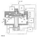
- the first vacuum pump 190is located above the upper chamber assembly 130 and is physically coupled to an upper surface thereof (see FIG. 1A ).
- the inlet 191 of the first vacuum pump 190is coupled to at least one annular volume, such as a first annular volume 352 coupled to second annular volume 312 , which in turn is coupled through extension 304 to one or more openings 305 that access process space 180 at a location below the plane of substrate 125 .
- the one or more openings 305are merely “below” the plane of the substrate 125 , but not directly below the substrate 125 itself. However, it is possible to arrange the one or more openings 305 at other locations within the process space 180 .
- the one or more openings 305may comprise a continuous annular opening, one or more slots, one or more orifices, or any combination thereof.
- the first vacuum pump 190is physically coupled to the upper chamber assembly 130 via the first vacuum valve 194 .
- intermediate connectionsmay be used such that the first vacuum pump is not actually supported by the upper chamber assembly.
- first vacuum pump 190may be more convenient to locate the first vacuum pump 190 above the process space 180 than below the process space 180 . In addition to space considerations, this may be due, for example, to the presence of the transfer space 182 and the process of translating the substrate stage 120 back and forth from the first and second position. Thus, a connection must be made to allow fluid communication between the first pump 190 , located above the process space 180 (and therefore above the substrate 125 ) and the one or more openings 305 which are preferably located below the substrate 125 .
- the inlet 191 of the first vacuum pump 190is in fluid communication with a first annular volume 352 that is in turn in fluid communication with a second annular volume 312 , whereby the first annular volume and the second annular volume are coupled or placed in fluid communication via one or more pumping ports 354 .
- the second annular volumeis typically coupled through extension 304 to one or more openings 305 that access process space 180 at a location below the plane of substrate 125 .
- locating the one or more openings 305 below the level of the substrate 125can impede particle accumulation released from the pump inlet 191 from reaching the substrate surface. Further, positioning the openings 305 below the substrate can cause a result that the flow of gas within the process space 180 will generally be downward and away from the center of the substrate 125 . Accordingly, any particulate accumulation will tend to occur beneath the level of the substrate 125 and will be less likely to contaminate the surface of the substrate 125 . Thus, causing vacuum flow from beneath the substrate 125 can reduce contamination of the substrate 125 .
- the one or more pumping ports 354may comprise two through-holes diametrically opposing one another (i.e., 180 degrees apart as relates to a circle which has the center of the substrate stage 120 as its center).
- the pumping ports 354allow gas to flow from the second annular volume 312 to the first annular volume 352 .
- the number of pumping portsmay be more or less, and their location may vary.
- the one or more openings 305may comprise two holes or slots diametrically opposing one another (i.e., 180 degrees apart). Furthermore, each slot can extend approximately 120 degrees in the azimuthal direction. However, the number of openings 305 may be more or less, and their location and size may vary.
- the pumping ports 354are offset in a vertical direction from the one or more openings 305 in order to alter the flow path from the one or more openings 305 , thus providing more symmetric pumping from the process space 180 .
- one aspect of the present inventionis to improve consistency of the process across the substrate 125 by evacuating the process space 180 uniformly so that all areas of the substrate 125 experience similar process conditions. If the first vacuum pump inlet 191 is not positioned directly above or below the center of the substrate 125 , inconsistent flow during pumping may arise. This is particularly true where pumping of the process space occurs through a limited volume opening 305 that is confined below the substrate. Accordingly, measures should be taken in order to compensate for any bias in flow created by positioning the first vacuum pump inlet 191 off-center to the substrate 125 .
- FIG. 8Ashows a cross section of the upper chamber assembly 130 of FIG. 1A .
- a process gas supply port 350through which process gas may be supplied to the plenum 142 .
- pumping ports 354which allow fluid communication between a second annular volume 312 (shown in FIG. 8B ) formed by the extension 304 and the first annular volume 352 . Accordingly, the path taken by gas pumped from the process space 180 will enter the one or more openings 305 , travel through the second annular volume 312 and then through the pumping ports 354 .
- the pumping portsare not directly above the openings 305 , and the gas is forced to change direction before passing through the pumping ports 354 .
- the gasAfter passing through the pumping ports 354 , the gas will enter a first annular volume 352 which is in fluid communication with the inlet 191 of the first vacuum pump 190 .
- FIG. 8Cshows a perspective cut-away view of one half of the upper chamber assembly, first annular volume 352 , second annular volume 312 , openings 305 and pumping ports 354 .
- the openings 305will each extend over an arc of approximately 30° on two sides of the processing space 180 .
- the shown pumping port 354extends over an arc of approximately 90° as shown in FIG. 8B , but other sizes and shapes are possible.
- the pumping port 354will have a mirrored counterpart on the opposite side of the chamber.
- the path and volume of gas pumped from the process space 180can be controlled.
- the systemis designed to achieve maximum pump conductance while also maintaining uniform pumping conditions.
- the combined area of the openings 305 and the pumping ports 354can be sized to match or exceed the opening area of the first pump inlet 191 .
- the conductance of the pumping portscan be sized and shaped to maximize conductance from the second annular volume 312 to the first annular volume 352 .
- the location of the pumping portscan be such that the gas pumped from the process space 180 encounters symmetrical conductances no matter which opening 305 it flows through, similar to the effect of placing the first vacuum pump inlet 191 directly over the center of the substrate 125 .
- gas flow during pumpingcan be made symmetric despite the off-center position of the first pump inlet 191 .
- the flow distance(the distance a gas must travel) between the one opening 305 and the first pump inlet 191 and the distance between another opening 305 and the first pump inlet are equal.
- the flow distancesare not equal, but, due to the shape and size of the cross-section of the annular volumes 312 and 352 , the conductances are equal.
- the first pump inlet 191is positioned at the 0° point as viewed from the top of the process space with the center of the substrate stage 120 defining the center of a circle with undetermined diameter.
- gas in the process space 180will more readily be pumped from the 0° area of the chamber than the 180° area, thus degrading process uniformity.
- first and second annular volumes connected only by selectively positioned pumping ports 354the pumping effect can be made more symmetrical.
- two pumping ports 354are included.
- One of the pumping ports 354is positioned at the 90° point on the above-described circle while the other pumping port 354 is positioned at the 270° point.
- gas pumped from the process space at the 180° pointmust travel approximately the same distance to the first pump inlet 191 as does gas pumped from the 0° point.
- gas pumped from the process space 180to travel a longer route to the pump inlet 191 than it would if a direct connection were made, better process uniformity can be achieved.
- pumping ports 354are located at the 0° and 180° points on the above-described circle. In another exemplary embodiment, more than two pumping ports 354 are included around the periphery of the process space 180 . Preferably, the pumping ports 354 are positioned symmetrically in the process space about a line defined by the center of the first pump inlet 191 and the center of the substrate stage 120 . For example, if two pumping ports 354 are provided, and the first pump inlet is at the 0° point, each pumping port 354 has a counterpart opening 354 mirrored about the line defined by the center of the first pump inlet 191 and the center of the substrate stage 120 .
- One such arrangementwould be to have one pumping port 354 at each of the 90° 0 and 270° points.
- Other arrangements with more pumping ports 354 in order to increase total conductanceare contemplated, but with more openings, the less balanced the vacuum pumping becomes.
- different sizes or shapes of pumping ports 354may be used.
- a small pumping port 354is included at the 0° and a large pumping port 354 is included at the 180° position.
- different sizes of pumping ports 354may be used.
- One benefit of differently sized pumping portsis that the overall size of the first annular space 352 may be reduced because it need only carry the gas flow of one pumping port 352 to the first vacuum pump inlet 191 ; the remainder of the gas flow travels straight up the small pumping port located at the 0° position and directly into the first vacuum pump inlet 191 , also located at the 0° position.
- the arrangement with pumping ports 354 located at the 90° and 270° positionsis easier to balance for symmetrical flow than is the arrangement where the ports are at the 0° and 180° positions.
- conductance of the portscan be varied by adjusting the shape of the pumping ports. For example, a long thin slot will have a lower conductance than a perfect circle of the same surface area. Thus, in some situations it may be beneficial to further reduce the overall size of the first annular space by providing long, thin pumping ports 354 in an area near the first pump inlet 191 while providing circular, wedge-shaped or square pumping ports 354 in areas further from the first pump inlet 191 .
- the shapes of the pumping ports 354may vary from the above-noted geometries.
- the above-described arrangementreduces contamination in the process space because the gas takes a path downward and away from the substrate 125 . Further, the arrangement allows the first vacuum pump 190 to reside above the process space 180 , out of the way of components such as the moving substrate stage 125 . Additionally, by incorporating the first annular volume 352 , the second annular volume 312 , and strategically placed pumping ports 354 , the pumping process can be made more uniform.
- FIGS. 3 , 4 , 5 , and 6illustrate several embodiments for sealing (and movably sealing) the substrate stage 120 with the upper chamber assembly 130 when the deposition system 101 is in a processing configuration.
- the systemincludes a sealing member that impedes the flow of gas between the process space and the transfer space.
- a seal of the sealing memberseparates the vacuum environment of the process space from the vacuum environment of the transfer space. By vacuum separating the process space from the transfer space, the seal is able to reduce leakage between the process space and the transfer space to less than 10-3 Torr-l/s and preferably less than 10-4 Torr-l/s.
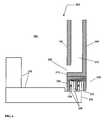
- FIG. 3is a schematic diagram illustrating a seal configuration for producing a seal between a flange 302 of the substrate stage 120 and an extension 304 from the upper chamber assembly 130 .
- a seal 306is located in a groove 308 of the flange 302 of the substrate stage 120 . Details of the seal 306 will be described below.
- the seal 306contacts a bottom plate 310 (i.e., a seal plate) of the extension 304 .
- a second annular volume 312is provided in the extension 304 for the purpose of evacuating gases from processing region 180 to pump 190 .
- the configuration shown in FIG. 3provides an adequate seal but does not accommodate considerable vertical translation without loss of the seal. For instance, only vertical motion less than a distance comparable to approximately one half of the seal 306 thickness can be tolerated before the seal looses contact with the bottom plate 310 .
- FIG. 4is a schematic diagram illustrating a seal configuration for producing a seal between the flange 302 of the substrate stage 120 and the extension 304 from the upper chamber assembly 130 .
- the seal 314is elongated in a vertical direction.
- the seal 314has a triangular cross section, the apex of which contacts the bottom plate 310 .
- the bottom plate 310includes a protective guard 316 that extends toward the flange 302 so as to protect the seal 314 from inadvertent material deposits or exposure to plasma species such as the above-noted plasma generated reducing agents.
- a recess 318is provided in the flange 302 of the substrate stage 120 .
- the configuration shown in FIG. 4permits a greater translation than the seal configuration shown in FIG. 3 .
- FIG. 5is a schematic diagram illustrating a seal configuration for producing a seal between the flange 302 of the substrate stage 120 and the extension 304 from the upper chamber assembly 130 .
- the seal configuration depicted in FIG. 5permits even greater translation of the substrate stage 120 in a vertical direction than the seal configurations shown in FIGS. 3 and 4 .
- the bottom plate 310connects to a bellows unit 320 which has a contact plate 322 (i.e., a seal plate).
- a guard 324can be provided in one embodiment of the present invention to protect the bellows unit 320 from inadvertent material deposits.
- the bellows unit 320being a metallic material such as stainless steel will not be prone to deterioration from plasma exposure.
- a recess 326can be provided in the flange 302 of the substrate stage 120 .
- FIG. 6is a schematic diagram illustrating a seal configuration for producing a seal between the flange 302 of the substrate stage 120 and the extension 304 from the upper chamber assembly 130 .
- the seal configuration depicted in FIG. 6permits even greater translation of the substrate stage 120 than the seal configurations shown in FIGS. 3 and 4 .
- the bottom plate 310connects to a slider-unit 328 .
- the slider unit 328has at least one longitudinal plate 330 extending in a vertical direction that engages an associated reception plate 332 on the flange 302 of the substrate stage 120 .
- the seal 334disposed on a side wall of either the longitudinal plate 330 or the receptor plate 332 to provide for the seal.
- the receptor plate 332is disposed in a recess 336 of the flange in order to protect the seal 334 from inadvertent material deposit or plasma deterioration.
- the seal 334can be a standard O-ring or preferably a tapered elastomer seal as shown in FIG. 6 , in which the seal for example has a triangular cross section whose apex is at a point of seal between the flange 302 of the substrate stage 120 and the upper chamber assembly 130 .
- the seal configuration depicted in FIG. 6permits even greater translation of the substrate stage without loss of seal than the seal configurations shown in FIGS. 3 and 4 .
- the longitudinal plate 330provides protection of the seal 334 from material deposit or plasma deterioration.
- the second volume (V 2 ) of the process space 180can be set to a volume in which the formation of plasma from the second process material leads to the formation of uniform plasma above the substrate, without loss of seal between the process space 180 and the vacuum in the lower assembly 132 .
- the ability according to the present invention to be able to provide a plasma process geometry of comparable uniformity to the process geometrypermits the present invention to perform consecutive processes or process steps, i.e., non-plasma and plasma, in the same system without the need to transfer the substrate between different processing systems, thereby saving process time and reducing surface contamination at the interfaces between the process films, leading to improved material properties for the resultant films.
- FIG. 7shows a process flow diagram of a process in accordance with one embodiment of the present invention.
- the process of FIG. 7may be performed by the processing system of FIGS. 1-2 , or any other suitable processing system.
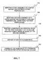
- the processincludes disposing a substrate in a process space of a processing system that is vacuum isolated from a transfer space of the processing system.
- a substrateis processed at either of a first position or a second position in the process space while maintaining vacuum isolation from the transfer space.
- a materialis deposited on the substrate at either the first position or the second position.
- the first assemblycan be maintained greater than or equal to 100 degrees C., while the second assembly can be maintained less than or equal to 100 degrees C.
- the first assemblycan be maintained greater than or equal to 50 degrees C., while the second assembly can be maintained less than or equal to 50 degrees C.
- the gas conductance from the process space to the transfer spaceto less than 10 ⁇ 3 Torr-l/s, and preferably less than 10 ⁇ 4 Torr-l/s.
- a process gas compositionin order to deposit a material, can be introduced to the process for vapor deposition of the material. Further, plasma can be formed from the process gas composition to enhance the vapor deposition rate.
- the material depositedcan be at least one of a metal, metal oxide, metal nitride, metal carbonitride, or a metal silicide.
- the material depositedcan be at least one of a tantalum film, a tantalum nitride film, or a tantalum carbonitride film.
- the processing systemcan be configured for at least one of an atomic layer deposition (ALD) process, a plasma enhanced ALD (PEALD) process, a chemical vapor deposition (CVD) process, or a plasma enhanced CVD (PECVD) process.
- ALDatomic layer deposition
- PEALDplasma enhanced ALD
- CVDchemical vapor deposition
- PECVDplasma enhanced CVD
- plasmacan be formed by applying radio frequency (RF) energy at a frequency from 0.1 to 100 MHz to a process gas in the process space.
- an electrodecan be connected to a RF power supply and configured to couple the RF energy into the process space.
- the substrate stageprior to forming the plasma, the volume of the process space is increased in order to facilitate conditions more conducive for plasma uniformity.
- the substrate stagecan be translated to a position that improves plasma uniformity of the vapor deposition process.
- the substrate stagecan be set to a position in which the plasma uniformity is better than 2% across a 200 mm diameter substrate or better than 1% across a 200 mm diameter substrate.
- the substrate stagecan be set to a position in which the plasma uniformity is better than 2% across a 300 mm diameter substrate or better than 1% across a 300 mm diameter substrate.
- a purge gascan be introduced after depositing the material.
- electromagnetic powercan be coupled to the vapor deposition system to release contaminants from at least one of the vapor deposition system or the substrate.
- the electromagnetic powercan be coupled into the vapor deposition system in the form of a plasma, an ultraviolet light, or a laser.
- controller 170can include a microprocessor, memory, and a digital I/O port capable of generating control voltages sufficient to communicate and activate inputs to deposition system 101 as well as monitor outputs from deposition system 101 .
- the controller 170may exchange information with the processing chamber 110 , substrate stage 120 , upper assembly 130 , lower chamber assembly 132 , process material supply system 140 , first power source 150 , substrate temperature control system 160 , first vacuum pump 190 , first vacuum valve 194 , second vacuum pump 192 , second vacuum valve 196 , and process volume adjustment system 122 .
- a program stored in the memorymay be utilized to activate the inputs to the aforementioned components of the deposition system 101 according to a process recipe in order to perform an etching process, or a deposition process.
- the controller 170can include a microprocessor, memory, and a digital I/O port capable of generating control voltages sufficient to communicate and activate inputs to deposition system 101 ( 101 ′) as well as monitor outputs from deposition system 101 ( 101 ′) in order to control and monitor the above-discussed processes for material deposition.
- the controller 170can include computer readable medium containing program instructions for execution to accomplish the steps described above in relation to FIG. 6 .
- the controller 170may be coupled to and may exchange information with the process chamber 110 , substrate stage 120 , upper assembly 130 , process material gas supply system 140 , power source 150 , substrate temperature controller 160 , first vacuum pumping system 190 , and/or second vacuum pumping system 192 .
- a program stored in the memorymay be utilized to activate the inputs to the aforementioned components of the deposition system 101 ( 101 ′) according to a process recipe in order to perform one of the above-described non-plasma or plasma enhanced deposition processes.
- controller 170is a DELL PRECISION WORKSTATION 610 , available from Dell Corporation, Austin, Tex.
- the controller 170may be implemented as a general-purpose computer system that performs a portion or all of the microprocessor based processing steps of the invention in response to a processor executing one or more sequences of one or more instructions contained in a memory. Such instructions may be read into the controller memory from another computer readable medium, such as a hard disk or a removable media drive.
- processors in a multi-processing arrangementmay also be employed as the controller microprocessor to execute the sequences of instructions contained in main memory.
- hard-wired circuitrymay be used in place of or in combination with software instructions. Thus, embodiments are not limited to any specific combination of hardware circuitry and software.
- the controller 170includes at least one computer readable medium or memory, such as the controller memory, for holding instructions programmed according to the teachings of the invention and for containing data structures, tables, records, or other data that may be necessary to implement the present invention.
- Examples of computer readable mediaare compact discs, hard disks, floppy disks, tape, magneto-optical disks, PROMs (EPROM, EEPROM, flash EPROM), DRAM, SRAM, SDRAM, or any other magnetic medium, compact discs (e.g., CD-ROM), or any other optical medium, punch cards, paper tape, or other physical medium with patterns of holes, a carrier wave (described below), or any other medium from which a computer can read.
- the present inventionincludes software for controlling the controller 170 , for driving a device or devices for implementing the invention, and/or for enabling the controller to interact with a human user.
- softwaremay include, but is not limited to, device drivers, operating systems, development tools, and applications software.
- Such computer readable mediafurther includes the computer program product of the present invention for performing all or a portion (if processing is distributed) of the processing performed in implementing the invention.
- the computer code devices of the present inventionmay be any interpretable or executable code mechanism, including but not limited to scripts, interpretable programs, dynamic link libraries (DLLs), Java classes, and complete executable programs. Moreover, parts of the processing of the present invention may be distributed for better performance, reliability, and/or cost.
- Non-volatile mediaincludes, for example, optical, magnetic disks, and magneto-optical disks, such as the hard disk or the removable media drive.
- Volatile mediaincludes dynamic memory, such as the main memory.
- various forms of computer readable mediamay be involved in carrying out one or more sequences of one or more instructions to the processor of the controller for execution.
- the instructionsmay initially be carried on a magnetic disk of a remote computer.
- the remote computercan load the instructions for implementing all or a portion of the present invention remotely into a dynamic memory and send the instructions over a network to the controller 170 .
- the controller 170may be locally located relative to the deposition system 101 ( 101 ′), or it may be remotely located relative to the deposition system 101 .
- the controller 170may exchange data with the deposition system 101 using at least one of a direct connection, an intranet, the Internet and a wireless connection.
- the controller 170may be coupled to an intranet at, for example, a customer site (i.e., a device maker, etc.), or it may be coupled to an intranet at, for example, a vendor site (i.e., an equipment manufacturer). Additionally, for example, the controller 170 may be coupled to the Internet.
- controllermay access, for example, the controller 170 to exchange data via at least one of a direct connection, an intranet, and the Internet.
- controller 170may exchange data with the deposition system 101 ( 101 ′) via a wireless connection.
Landscapes
- Chemical & Material Sciences (AREA)
- General Chemical & Material Sciences (AREA)
- Chemical Kinetics & Catalysis (AREA)
- Engineering & Computer Science (AREA)
- Materials Engineering (AREA)
- Mechanical Engineering (AREA)
- Metallurgy (AREA)
- Organic Chemistry (AREA)
- Chemical Vapour Deposition (AREA)
- Formation Of Insulating Films (AREA)
Abstract
Description
Claims (11)
Priority Applications (2)
| Application Number | Priority Date | Filing Date | Title |
|---|---|---|---|
| US11/369,883US7740705B2 (en) | 2006-03-08 | 2006-03-08 | Exhaust apparatus configured to reduce particle contamination in a deposition system |
| JP2007059045AJP5242066B2 (en) | 2006-03-08 | 2007-03-08 | An exhaust system configured to reduce particle contamination in a deposition system |
Applications Claiming Priority (1)
| Application Number | Priority Date | Filing Date | Title |
|---|---|---|---|
| US11/369,883US7740705B2 (en) | 2006-03-08 | 2006-03-08 | Exhaust apparatus configured to reduce particle contamination in a deposition system |
Publications (2)
| Publication Number | Publication Date |
|---|---|
| US20070212484A1 US20070212484A1 (en) | 2007-09-13 |
| US7740705B2true US7740705B2 (en) | 2010-06-22 |
Family
ID=38479269
Family Applications (1)
| Application Number | Title | Priority Date | Filing Date |
|---|---|---|---|
| US11/369,883Expired - Fee RelatedUS7740705B2 (en) | 2006-03-08 | 2006-03-08 | Exhaust apparatus configured to reduce particle contamination in a deposition system |
Country Status (2)
| Country | Link |
|---|---|
| US (1) | US7740705B2 (en) |
| JP (1) | JP5242066B2 (en) |
Cited By (413)
| Publication number | Priority date | Publication date | Assignee | Title |
|---|---|---|---|---|
| US20090044753A1 (en)* | 2006-06-23 | 2009-02-19 | Deenesh Padhi | Methods to improve the in-film defectivity of pecvd amorphous carbon films |
| US20100159703A1 (en)* | 2008-12-19 | 2010-06-24 | Andreas Fischer | Methods and apparatus for dual confinement and ultra-high pressure in an adjustable gap plasma chamber |
| US20100307415A1 (en)* | 2009-04-06 | 2010-12-09 | Eric Shero | Semiconductor processing reactor and components thereof |
| US20110305836A1 (en)* | 2009-03-10 | 2011-12-15 | Mitsui Engineering & Shipbuilding Co., Ltd. | Atomic layer deposition apparatus and thin film forming method |
| US20120160173A1 (en)* | 2010-12-23 | 2012-06-28 | Richard Endo | Vapor Based Processing System with Purge Mode |
| US20130025539A1 (en)* | 2007-05-21 | 2013-01-31 | Centrotherm Photovoltaics Ag | Device for doping, deposition or oxidation of semiconductor material at low pressure |
| US20130129577A1 (en)* | 2011-11-23 | 2013-05-23 | ASM Holding B.V. | Chamber sealing member |
| US20130224965A1 (en)* | 2012-02-29 | 2013-08-29 | Kabushiki Kaisha Toshiba | Semiconductor manufacturing apparatus and manufacturing method of semiconductor device |
| US20140227861A1 (en)* | 2013-02-08 | 2014-08-14 | Taiwan Semiconductor Manufacturing Co., Ltd. | Bottom-Up PEALD Process |
| US8877655B2 (en) | 2010-05-07 | 2014-11-04 | Asm America, Inc. | Systems and methods for thin-film deposition of metal oxides using excited nitrogen-oxygen species |
| US8883270B2 (en) | 2009-08-14 | 2014-11-11 | Asm America, Inc. | Systems and methods for thin-film deposition of metal oxides using excited nitrogen—oxygen species |
| US8894870B2 (en) | 2013-02-01 | 2014-11-25 | Asm Ip Holding B.V. | Multi-step method and apparatus for etching compounds containing a metal |
| US8933375B2 (en) | 2012-06-27 | 2015-01-13 | Asm Ip Holding B.V. | Susceptor heater and method of heating a substrate |
| US8946830B2 (en) | 2012-04-04 | 2015-02-03 | Asm Ip Holdings B.V. | Metal oxide protective layer for a semiconductor device |
| US8986456B2 (en) | 2006-10-10 | 2015-03-24 | Asm America, Inc. | Precursor delivery system |
| US8993054B2 (en) | 2013-07-12 | 2015-03-31 | Asm Ip Holding B.V. | Method and system to reduce outgassing in a reaction chamber |
| US9017481B1 (en) | 2011-10-28 | 2015-04-28 | Asm America, Inc. | Process feed management for semiconductor substrate processing |
| US9018111B2 (en) | 2013-07-22 | 2015-04-28 | Asm Ip Holding B.V. | Semiconductor reaction chamber with plasma capabilities |
| US9021985B2 (en) | 2012-09-12 | 2015-05-05 | Asm Ip Holdings B.V. | Process gas management for an inductively-coupled plasma deposition reactor |
| US9029253B2 (en) | 2012-05-02 | 2015-05-12 | Asm Ip Holding B.V. | Phase-stabilized thin films, structures and devices including the thin films, and methods of forming same |
| US9096931B2 (en) | 2011-10-27 | 2015-08-04 | Asm America, Inc | Deposition valve assembly and method of heating the same |
| US9117866B2 (en) | 2012-07-31 | 2015-08-25 | Asm Ip Holding B.V. | Apparatus and method for calculating a wafer position in a processing chamber under process conditions |
| US9167625B2 (en) | 2011-11-23 | 2015-10-20 | Asm Ip Holding B.V. | Radiation shielding for a substrate holder |
| US9169975B2 (en) | 2012-08-28 | 2015-10-27 | Asm Ip Holding B.V. | Systems and methods for mass flow controller verification |
| US9177784B2 (en) | 2012-05-07 | 2015-11-03 | Asm Ip Holdings B.V. | Semiconductor device dielectric interface layer |
| US9202727B2 (en) | 2012-03-02 | 2015-12-01 | ASM IP Holding | Susceptor heater shim |
| US9240412B2 (en) | 2013-09-27 | 2016-01-19 | Asm Ip Holding B.V. | Semiconductor structure and device and methods of forming same using selective epitaxial process |
| US9324811B2 (en) | 2012-09-26 | 2016-04-26 | Asm Ip Holding B.V. | Structures and devices including a tensile-stressed silicon arsenic layer and methods of forming same |
| US9341296B2 (en) | 2011-10-27 | 2016-05-17 | Asm America, Inc. | Heater jacket for a fluid line |
| US9396934B2 (en) | 2013-08-14 | 2016-07-19 | Asm Ip Holding B.V. | Methods of forming films including germanium tin and structures and devices including the films |
| US9404587B2 (en) | 2014-04-24 | 2016-08-02 | ASM IP Holding B.V | Lockout tagout for semiconductor vacuum valve |
| US9447498B2 (en) | 2014-03-18 | 2016-09-20 | Asm Ip Holding B.V. | Method for performing uniform processing in gas system-sharing multiple reaction chambers |
| US9455138B1 (en) | 2015-11-10 | 2016-09-27 | Asm Ip Holding B.V. | Method for forming dielectric film in trenches by PEALD using H-containing gas |
| US9478415B2 (en) | 2015-02-13 | 2016-10-25 | Asm Ip Holding B.V. | Method for forming film having low resistance and shallow junction depth |
| US9484191B2 (en) | 2013-03-08 | 2016-11-01 | Asm Ip Holding B.V. | Pulsed remote plasma method and system |
| US9543180B2 (en) | 2014-08-01 | 2017-01-10 | Asm Ip Holding B.V. | Apparatus and method for transporting wafers between wafer carrier and process tool under vacuum |
| US9556516B2 (en) | 2013-10-09 | 2017-01-31 | ASM IP Holding B.V | Method for forming Ti-containing film by PEALD using TDMAT or TDEAT |
| US9558931B2 (en) | 2012-07-27 | 2017-01-31 | Asm Ip Holding B.V. | System and method for gas-phase sulfur passivation of a semiconductor surface |
| US9589770B2 (en) | 2013-03-08 | 2017-03-07 | Asm Ip Holding B.V. | Method and systems for in-situ formation of intermediate reactive species |
| US9605343B2 (en) | 2013-11-13 | 2017-03-28 | Asm Ip Holding B.V. | Method for forming conformal carbon films, structures conformal carbon film, and system of forming same |
| US9607837B1 (en) | 2015-12-21 | 2017-03-28 | Asm Ip Holding B.V. | Method for forming silicon oxide cap layer for solid state diffusion process |
| US9627221B1 (en) | 2015-12-28 | 2017-04-18 | Asm Ip Holding B.V. | Continuous process incorporating atomic layer etching |
| US9640416B2 (en) | 2012-12-26 | 2017-05-02 | Asm Ip Holding B.V. | Single-and dual-chamber module-attachable wafer-handling chamber |
| US9647114B2 (en) | 2015-08-14 | 2017-05-09 | Asm Ip Holding B.V. | Methods of forming highly p-type doped germanium tin films and structures and devices including the films |
| US9657845B2 (en) | 2014-10-07 | 2017-05-23 | Asm Ip Holding B.V. | Variable conductance gas distribution apparatus and method |
| US9659799B2 (en) | 2012-08-28 | 2017-05-23 | Asm Ip Holding B.V. | Systems and methods for dynamic semiconductor process scheduling |
| US9711345B2 (en) | 2015-08-25 | 2017-07-18 | Asm Ip Holding B.V. | Method for forming aluminum nitride-based film by PEALD |
| US9735024B2 (en) | 2015-12-28 | 2017-08-15 | Asm Ip Holding B.V. | Method of atomic layer etching using functional group-containing fluorocarbon |
| US9754779B1 (en) | 2016-02-19 | 2017-09-05 | Asm Ip Holding B.V. | Method for forming silicon nitride film selectively on sidewalls or flat surfaces of trenches |
| US9793148B2 (en) | 2011-06-22 | 2017-10-17 | Asm Japan K.K. | Method for positioning wafers in multiple wafer transport |
| US9793135B1 (en) | 2016-07-14 | 2017-10-17 | ASM IP Holding B.V | Method of cyclic dry etching using etchant film |
| US9793115B2 (en) | 2013-08-14 | 2017-10-17 | Asm Ip Holding B.V. | Structures and devices including germanium-tin films and methods of forming same |
| US9812320B1 (en) | 2016-07-28 | 2017-11-07 | Asm Ip Holding B.V. | Method and apparatus for filling a gap |
| US9859151B1 (en) | 2016-07-08 | 2018-01-02 | Asm Ip Holding B.V. | Selective film deposition method to form air gaps |
| US9887082B1 (en) | 2016-07-28 | 2018-02-06 | Asm Ip Holding B.V. | Method and apparatus for filling a gap |
| US9890456B2 (en) | 2014-08-21 | 2018-02-13 | Asm Ip Holding B.V. | Method and system for in situ formation of gas-phase compounds |
| US9891521B2 (en) | 2014-11-19 | 2018-02-13 | Asm Ip Holding B.V. | Method for depositing thin film |
| US9899291B2 (en) | 2015-07-13 | 2018-02-20 | Asm Ip Holding B.V. | Method for protecting layer by forming hydrocarbon-based extremely thin film |
| US9899405B2 (en) | 2014-12-22 | 2018-02-20 | Asm Ip Holding B.V. | Semiconductor device and manufacturing method thereof |
| US9905420B2 (en) | 2015-12-01 | 2018-02-27 | Asm Ip Holding B.V. | Methods of forming silicon germanium tin films and structures and devices including the films |
| US9909214B2 (en) | 2015-10-15 | 2018-03-06 | Asm Ip Holding B.V. | Method for depositing dielectric film in trenches by PEALD |
| US9916980B1 (en) | 2016-12-15 | 2018-03-13 | Asm Ip Holding B.V. | Method of forming a structure on a substrate |
| US9960072B2 (en) | 2015-09-29 | 2018-05-01 | Asm Ip Holding B.V. | Variable adjustment for precise matching of multiple chamber cavity housings |
| US10032628B2 (en) | 2016-05-02 | 2018-07-24 | Asm Ip Holding B.V. | Source/drain performance through conformal solid state doping |
| US10043661B2 (en) | 2015-07-13 | 2018-08-07 | Asm Ip Holding B.V. | Method for protecting layer by forming hydrocarbon-based extremely thin film |
| US10083836B2 (en) | 2015-07-24 | 2018-09-25 | Asm Ip Holding B.V. | Formation of boron-doped titanium metal films with high work function |
| US10090316B2 (en) | 2016-09-01 | 2018-10-02 | Asm Ip Holding B.V. | 3D stacked multilayer semiconductor memory using doped select transistor channel |
| US10087522B2 (en) | 2016-04-21 | 2018-10-02 | Asm Ip Holding B.V. | Deposition of metal borides |
| US10087525B2 (en) | 2015-08-04 | 2018-10-02 | Asm Ip Holding B.V. | Variable gap hard stop design |
| USD830981S1 (en) | 2017-04-07 | 2018-10-16 | Asm Ip Holding B.V. | Susceptor for semiconductor substrate processing apparatus |
| US10103040B1 (en) | 2017-03-31 | 2018-10-16 | Asm Ip Holding B.V. | Apparatus and method for manufacturing a semiconductor device |
| US10134757B2 (en) | 2016-11-07 | 2018-11-20 | Asm Ip Holding B.V. | Method of processing a substrate and a device manufactured by using the method |
| US10167557B2 (en) | 2014-03-18 | 2019-01-01 | Asm Ip Holding B.V. | Gas distribution system, reactor including the system, and methods of using the same |
| US10177025B2 (en) | 2016-07-28 | 2019-01-08 | Asm Ip Holding B.V. | Method and apparatus for filling a gap |
| US10179947B2 (en) | 2013-11-26 | 2019-01-15 | Asm Ip Holding B.V. | Method for forming conformal nitrided, oxidized, or carbonized dielectric film by atomic layer deposition |
| US10190213B2 (en) | 2016-04-21 | 2019-01-29 | Asm Ip Holding B.V. | Deposition of metal borides |
| US10211308B2 (en) | 2015-10-21 | 2019-02-19 | Asm Ip Holding B.V. | NbMC layers |
| US10229833B2 (en) | 2016-11-01 | 2019-03-12 | Asm Ip Holding B.V. | Methods for forming a transition metal nitride film on a substrate by atomic layer deposition and related semiconductor device structures |
| US10236177B1 (en) | 2017-08-22 | 2019-03-19 | ASM IP Holding B.V.. | Methods for depositing a doped germanium tin semiconductor and related semiconductor device structures |
| US10249577B2 (en) | 2016-05-17 | 2019-04-02 | Asm Ip Holding B.V. | Method of forming metal interconnection and method of fabricating semiconductor apparatus using the method |
| US10249524B2 (en) | 2017-08-09 | 2019-04-02 | Asm Ip Holding B.V. | Cassette holder assembly for a substrate cassette and holding member for use in such assembly |
| US10262859B2 (en) | 2016-03-24 | 2019-04-16 | Asm Ip Holding B.V. | Process for forming a film on a substrate using multi-port injection assemblies |
| US10269558B2 (en) | 2016-12-22 | 2019-04-23 | Asm Ip Holding B.V. | Method of forming a structure on a substrate |
| US10276355B2 (en) | 2015-03-12 | 2019-04-30 | Asm Ip Holding B.V. | Multi-zone reactor, system including the reactor, and method of using the same |
| US10283353B2 (en) | 2017-03-29 | 2019-05-07 | Asm Ip Holding B.V. | Method of reforming insulating film deposited on substrate with recess pattern |
| US10290508B1 (en) | 2017-12-05 | 2019-05-14 | Asm Ip Holding B.V. | Method for forming vertical spacers for spacer-defined patterning |
| US10312055B2 (en) | 2017-07-26 | 2019-06-04 | Asm Ip Holding B.V. | Method of depositing film by PEALD using negative bias |
| US10319588B2 (en) | 2017-10-10 | 2019-06-11 | Asm Ip Holding B.V. | Method for depositing a metal chalcogenide on a substrate by cyclical deposition |
| US10322384B2 (en) | 2015-11-09 | 2019-06-18 | Asm Ip Holding B.V. | Counter flow mixer for process chamber |
| US10340135B2 (en) | 2016-11-28 | 2019-07-02 | Asm Ip Holding B.V. | Method of topologically restricted plasma-enhanced cyclic deposition of silicon or metal nitride |
| US10343920B2 (en) | 2016-03-18 | 2019-07-09 | Asm Ip Holding B.V. | Aligned carbon nanotubes |
| US10358721B2 (en)* | 2015-10-22 | 2019-07-23 | Asm Ip Holding B.V. | Semiconductor manufacturing system including deposition apparatus |
| US10364496B2 (en) | 2011-06-27 | 2019-07-30 | Asm Ip Holding B.V. | Dual section module having shared and unshared mass flow controllers |
| US10367080B2 (en) | 2016-05-02 | 2019-07-30 | Asm Ip Holding B.V. | Method of forming a germanium oxynitride film |
| US10381219B1 (en) | 2018-10-25 | 2019-08-13 | Asm Ip Holding B.V. | Methods for forming a silicon nitride film |
| US10381226B2 (en) | 2016-07-27 | 2019-08-13 | Asm Ip Holding B.V. | Method of processing substrate |
| US10378106B2 (en) | 2008-11-14 | 2019-08-13 | Asm Ip Holding B.V. | Method of forming insulation film by modified PEALD |
| US10388509B2 (en) | 2016-06-28 | 2019-08-20 | Asm Ip Holding B.V. | Formation of epitaxial layers via dislocation filtering |
| US10388513B1 (en) | 2018-07-03 | 2019-08-20 | Asm Ip Holding B.V. | Method for depositing silicon-free carbon-containing film as gap-fill layer by pulse plasma-assisted deposition |
| US10395919B2 (en) | 2016-07-28 | 2019-08-27 | Asm Ip Holding B.V. | Method and apparatus for filling a gap |
| US10403504B2 (en) | 2017-10-05 | 2019-09-03 | Asm Ip Holding B.V. | Method for selectively depositing a metallic film on a substrate |
| US10410943B2 (en) | 2016-10-13 | 2019-09-10 | Asm Ip Holding B.V. | Method for passivating a surface of a semiconductor and related systems |
| US10435790B2 (en) | 2016-11-01 | 2019-10-08 | Asm Ip Holding B.V. | Method of subatmospheric plasma-enhanced ALD using capacitively coupled electrodes with narrow gap |
| US10446393B2 (en) | 2017-05-08 | 2019-10-15 | Asm Ip Holding B.V. | Methods for forming silicon-containing epitaxial layers and related semiconductor device structures |
| US10458018B2 (en) | 2015-06-26 | 2019-10-29 | Asm Ip Holding B.V. | Structures including metal carbide material, devices including the structures, and methods of forming same |
| US10468261B2 (en) | 2017-02-15 | 2019-11-05 | Asm Ip Holding B.V. | Methods for forming a metallic film on a substrate by cyclical deposition and related semiconductor device structures |
| US10468251B2 (en) | 2016-02-19 | 2019-11-05 | Asm Ip Holding B.V. | Method for forming spacers using silicon nitride film for spacer-defined multiple patterning |
| US10483099B1 (en) | 2018-07-26 | 2019-11-19 | Asm Ip Holding B.V. | Method for forming thermally stable organosilicon polymer film |
| US10504742B2 (en) | 2017-05-31 | 2019-12-10 | Asm Ip Holding B.V. | Method of atomic layer etching using hydrogen plasma |
| US10501866B2 (en) | 2016-03-09 | 2019-12-10 | Asm Ip Holding B.V. | Gas distribution apparatus for improved film uniformity in an epitaxial system |
| US10510536B2 (en) | 2018-03-29 | 2019-12-17 | Asm Ip Holding B.V. | Method of depositing a co-doped polysilicon film on a surface of a substrate within a reaction chamber |
| US10529563B2 (en) | 2017-03-29 | 2020-01-07 | Asm Ip Holdings B.V. | Method for forming doped metal oxide films on a substrate by cyclical deposition and related semiconductor device structures |
| US10529542B2 (en) | 2015-03-11 | 2020-01-07 | Asm Ip Holdings B.V. | Cross-flow reactor and method |
| US10529554B2 (en) | 2016-02-19 | 2020-01-07 | Asm Ip Holding B.V. | Method for forming silicon nitride film selectively on sidewalls or flat surfaces of trenches |
| US10535516B2 (en) | 2018-02-01 | 2020-01-14 | Asm Ip Holdings B.V. | Method for depositing a semiconductor structure on a surface of a substrate and related semiconductor structures |
| US10541333B2 (en) | 2017-07-19 | 2020-01-21 | Asm Ip Holding B.V. | Method for depositing a group IV semiconductor and related semiconductor device structures |
| US10559458B1 (en) | 2018-11-26 | 2020-02-11 | Asm Ip Holding B.V. | Method of forming oxynitride film |
| US10590535B2 (en) | 2017-07-26 | 2020-03-17 | Asm Ip Holdings B.V. | Chemical treatment, deposition and/or infiltration apparatus and method for using the same |
| US10600673B2 (en) | 2015-07-07 | 2020-03-24 | Asm Ip Holding B.V. | Magnetic susceptor to baseplate seal |
| US10605530B2 (en) | 2017-07-26 | 2020-03-31 | Asm Ip Holding B.V. | Assembly of a liner and a flange for a vertical furnace as well as the liner and the vertical furnace |
| US10607895B2 (en) | 2017-09-18 | 2020-03-31 | Asm Ip Holdings B.V. | Method for forming a semiconductor device structure comprising a gate fill metal |
| USD880437S1 (en) | 2018-02-01 | 2020-04-07 | Asm Ip Holding B.V. | Gas supply plate for semiconductor manufacturing apparatus |
| US10612137B2 (en) | 2016-07-08 | 2020-04-07 | Asm Ip Holdings B.V. | Organic reactants for atomic layer deposition |
| US10612136B2 (en) | 2018-06-29 | 2020-04-07 | ASM IP Holding, B.V. | Temperature-controlled flange and reactor system including same |
| US10643904B2 (en) | 2016-11-01 | 2020-05-05 | Asm Ip Holdings B.V. | Methods for forming a semiconductor device and related semiconductor device structures |
| US10643826B2 (en) | 2016-10-26 | 2020-05-05 | Asm Ip Holdings B.V. | Methods for thermally calibrating reaction chambers |
| US10658181B2 (en) | 2018-02-20 | 2020-05-19 | Asm Ip Holding B.V. | Method of spacer-defined direct patterning in semiconductor fabrication |
| US10658205B2 (en) | 2017-09-28 | 2020-05-19 | Asm Ip Holdings B.V. | Chemical dispensing apparatus and methods for dispensing a chemical to a reaction chamber |
| US10655221B2 (en) | 2017-02-09 | 2020-05-19 | Asm Ip Holding B.V. | Method for depositing oxide film by thermal ALD and PEALD |
| US10685834B2 (en) | 2017-07-05 | 2020-06-16 | Asm Ip Holdings B.V. | Methods for forming a silicon germanium tin layer and related semiconductor device structures |
| US10683571B2 (en) | 2014-02-25 | 2020-06-16 | Asm Ip Holding B.V. | Gas supply manifold and method of supplying gases to chamber using same |
| US10692741B2 (en) | 2017-08-08 | 2020-06-23 | Asm Ip Holdings B.V. | Radiation shield |
| US10707106B2 (en) | 2011-06-06 | 2020-07-07 | Asm Ip Holding B.V. | High-throughput semiconductor-processing apparatus equipped with multiple dual-chamber modules |
| US10714315B2 (en) | 2012-10-12 | 2020-07-14 | Asm Ip Holdings B.V. | Semiconductor reaction chamber showerhead |
| US10714335B2 (en) | 2017-04-25 | 2020-07-14 | Asm Ip Holding B.V. | Method of depositing thin film and method of manufacturing semiconductor device |
| US10714350B2 (en) | 2016-11-01 | 2020-07-14 | ASM IP Holdings, B.V. | Methods for forming a transition metal niobium nitride film on a substrate by atomic layer deposition and related semiconductor device structures |
| US10714385B2 (en) | 2016-07-19 | 2020-07-14 | Asm Ip Holding B.V. | Selective deposition of tungsten |
| US10734244B2 (en) | 2017-11-16 | 2020-08-04 | Asm Ip Holding B.V. | Method of processing a substrate and a device manufactured by the same |
| US10734497B2 (en) | 2017-07-18 | 2020-08-04 | Asm Ip Holding B.V. | Methods for forming a semiconductor device structure and related semiconductor device structures |
| US10731249B2 (en) | 2018-02-15 | 2020-08-04 | Asm Ip Holding B.V. | Method of forming a transition metal containing film on a substrate by a cyclical deposition process, a method for supplying a transition metal halide compound to a reaction chamber, and related vapor deposition apparatus |
| US10755922B2 (en) | 2018-07-03 | 2020-08-25 | Asm Ip Holding B.V. | Method for depositing silicon-free carbon-containing film as gap-fill layer by pulse plasma-assisted deposition |
| US10767789B2 (en) | 2018-07-16 | 2020-09-08 | Asm Ip Holding B.V. | Diaphragm valves, valve components, and methods for forming valve components |
| US10770336B2 (en) | 2017-08-08 | 2020-09-08 | Asm Ip Holding B.V. | Substrate lift mechanism and reactor including same |
| US10770286B2 (en) | 2017-05-08 | 2020-09-08 | Asm Ip Holdings B.V. | Methods for selectively forming a silicon nitride film on a substrate and related semiconductor device structures |
| US10797133B2 (en) | 2018-06-21 | 2020-10-06 | Asm Ip Holding B.V. | Method for depositing a phosphorus doped silicon arsenide film and related semiconductor device structures |
| US10804098B2 (en) | 2009-08-14 | 2020-10-13 | Asm Ip Holding B.V. | Systems and methods for thin-film deposition of metal oxides using excited nitrogen-oxygen species |
| US10811256B2 (en) | 2018-10-16 | 2020-10-20 | Asm Ip Holding B.V. | Method for etching a carbon-containing feature |
| US10818758B2 (en) | 2018-11-16 | 2020-10-27 | Asm Ip Holding B.V. | Methods for forming a metal silicate film on a substrate in a reaction chamber and related semiconductor device structures |
| USD900036S1 (en) | 2017-08-24 | 2020-10-27 | Asm Ip Holding B.V. | Heater electrical connector and adapter |
| US10829852B2 (en) | 2018-08-16 | 2020-11-10 | Asm Ip Holding B.V. | Gas distribution device for a wafer processing apparatus |
| US10847366B2 (en) | 2018-11-16 | 2020-11-24 | Asm Ip Holding B.V. | Methods for depositing a transition metal chalcogenide film on a substrate by a cyclical deposition process |
| US10847371B2 (en) | 2018-03-27 | 2020-11-24 | Asm Ip Holding B.V. | Method of forming an electrode on a substrate and a semiconductor device structure including an electrode |
| US10847365B2 (en) | 2018-10-11 | 2020-11-24 | Asm Ip Holding B.V. | Method of forming conformal silicon carbide film by cyclic CVD |
| US10844484B2 (en) | 2017-09-22 | 2020-11-24 | Asm Ip Holding B.V. | Apparatus for dispensing a vapor phase reactant to a reaction chamber and related methods |
| USD903477S1 (en) | 2018-01-24 | 2020-12-01 | Asm Ip Holdings B.V. | Metal clamp |
| US10854498B2 (en) | 2011-07-15 | 2020-12-01 | Asm Ip Holding B.V. | Wafer-supporting device and method for producing same |
| US10858737B2 (en) | 2014-07-28 | 2020-12-08 | Asm Ip Holding B.V. | Showerhead assembly and components thereof |
| US10867788B2 (en) | 2016-12-28 | 2020-12-15 | Asm Ip Holding B.V. | Method of forming a structure on a substrate |
| US10865475B2 (en) | 2016-04-21 | 2020-12-15 | Asm Ip Holding B.V. | Deposition of metal borides and silicides |
| US10867786B2 (en) | 2018-03-30 | 2020-12-15 | Asm Ip Holding B.V. | Substrate processing method |
| US10872771B2 (en) | 2018-01-16 | 2020-12-22 | Asm Ip Holding B. V. | Method for depositing a material film on a substrate within a reaction chamber by a cyclical deposition process and related device structures |
| US10886123B2 (en) | 2017-06-02 | 2021-01-05 | Asm Ip Holding B.V. | Methods for forming low temperature semiconductor layers and related semiconductor device structures |
| US10883175B2 (en) | 2018-08-09 | 2021-01-05 | Asm Ip Holding B.V. | Vertical furnace for processing substrates and a liner for use therein |
| US10892156B2 (en) | 2017-05-08 | 2021-01-12 | Asm Ip Holding B.V. | Methods for forming a silicon nitride film on a substrate and related semiconductor device structures |
| US10896820B2 (en) | 2018-02-14 | 2021-01-19 | Asm Ip Holding B.V. | Method for depositing a ruthenium-containing film on a substrate by a cyclical deposition process |
| US10910262B2 (en) | 2017-11-16 | 2021-02-02 | Asm Ip Holding B.V. | Method of selectively depositing a capping layer structure on a semiconductor device structure |
| US10914004B2 (en) | 2018-06-29 | 2021-02-09 | Asm Ip Holding B.V. | Thin-film deposition method and manufacturing method of semiconductor device |
| US10923344B2 (en) | 2017-10-30 | 2021-02-16 | Asm Ip Holding B.V. | Methods for forming a semiconductor structure and related semiconductor structures |
| US10928731B2 (en) | 2017-09-21 | 2021-02-23 | Asm Ip Holding B.V. | Method of sequential infiltration synthesis treatment of infiltrateable material and structures and devices formed using same |
| US10934619B2 (en) | 2016-11-15 | 2021-03-02 | Asm Ip Holding B.V. | Gas supply unit and substrate processing apparatus including the gas supply unit |
| US10941490B2 (en) | 2014-10-07 | 2021-03-09 | Asm Ip Holding B.V. | Multiple temperature range susceptor, assembly, reactor and system including the susceptor, and methods of using the same |
| US10975470B2 (en) | 2018-02-23 | 2021-04-13 | Asm Ip Holding B.V. | Apparatus for detecting or monitoring for a chemical precursor in a high temperature environment |
| US11001925B2 (en) | 2016-12-19 | 2021-05-11 | Asm Ip Holding B.V. | Substrate processing apparatus |
| US11018002B2 (en) | 2017-07-19 | 2021-05-25 | Asm Ip Holding B.V. | Method for selectively depositing a Group IV semiconductor and related semiconductor device structures |
| US11018047B2 (en) | 2018-01-25 | 2021-05-25 | Asm Ip Holding B.V. | Hybrid lift pin |
| US11015245B2 (en) | 2014-03-19 | 2021-05-25 | Asm Ip Holding B.V. | Gas-phase reactor and system having exhaust plenum and components thereof |
| US11022879B2 (en) | 2017-11-24 | 2021-06-01 | Asm Ip Holding B.V. | Method of forming an enhanced unexposed photoresist layer |
| US11024523B2 (en) | 2018-09-11 | 2021-06-01 | Asm Ip Holding B.V. | Substrate processing apparatus and method |
| US11031242B2 (en) | 2018-11-07 | 2021-06-08 | Asm Ip Holding B.V. | Methods for depositing a boron doped silicon germanium film |
| USD922229S1 (en) | 2019-06-05 | 2021-06-15 | Asm Ip Holding B.V. | Device for controlling a temperature of a gas supply unit |
| US11049751B2 (en) | 2018-09-14 | 2021-06-29 | Asm Ip Holding B.V. | Cassette supply system to store and handle cassettes and processing apparatus equipped therewith |
| US11056567B2 (en) | 2018-05-11 | 2021-07-06 | Asm Ip Holding B.V. | Method of forming a doped metal carbide film on a substrate and related semiconductor device structures |
| US11056344B2 (en) | 2017-08-30 | 2021-07-06 | Asm Ip Holding B.V. | Layer forming method |
| US11053591B2 (en) | 2018-08-06 | 2021-07-06 | Asm Ip Holding B.V. | Multi-port gas injection system and reactor system including same |
| US11069510B2 (en) | 2017-08-30 | 2021-07-20 | Asm Ip Holding B.V. | Substrate processing apparatus |
| US11081345B2 (en) | 2018-02-06 | 2021-08-03 | Asm Ip Holding B.V. | Method of post-deposition treatment for silicon oxide film |
| US11088002B2 (en) | 2018-03-29 | 2021-08-10 | Asm Ip Holding B.V. | Substrate rack and a substrate processing system and method |
| US11087997B2 (en) | 2018-10-31 | 2021-08-10 | Asm Ip Holding B.V. | Substrate processing apparatus for processing substrates |
| US11114294B2 (en) | 2019-03-08 | 2021-09-07 | Asm Ip Holding B.V. | Structure including SiOC layer and method of forming same |
| US11114283B2 (en)* | 2018-03-16 | 2021-09-07 | Asm Ip Holding B.V. | Reactor, system including the reactor, and methods of manufacturing and using same |
| USD930782S1 (en) | 2019-08-22 | 2021-09-14 | Asm Ip Holding B.V. | Gas distributor |
| US11127589B2 (en) | 2019-02-01 | 2021-09-21 | Asm Ip Holding B.V. | Method of topology-selective film formation of silicon oxide |
| US11127617B2 (en) | 2017-11-27 | 2021-09-21 | Asm Ip Holding B.V. | Storage device for storing wafer cassettes for use with a batch furnace |
| USD931978S1 (en) | 2019-06-27 | 2021-09-28 | Asm Ip Holding B.V. | Showerhead vacuum transport |
| US11139191B2 (en) | 2017-08-09 | 2021-10-05 | Asm Ip Holding B.V. | Storage apparatus for storing cassettes for substrates and processing apparatus equipped therewith |
| US11139308B2 (en) | 2015-12-29 | 2021-10-05 | Asm Ip Holding B.V. | Atomic layer deposition of III-V compounds to form V-NAND devices |
| US11158513B2 (en) | 2018-12-13 | 2021-10-26 | Asm Ip Holding B.V. | Methods for forming a rhenium-containing film on a substrate by a cyclical deposition process and related semiconductor device structures |
| US11171025B2 (en) | 2019-01-22 | 2021-11-09 | Asm Ip Holding B.V. | Substrate processing device |
| USD935572S1 (en) | 2019-05-24 | 2021-11-09 | Asm Ip Holding B.V. | Gas channel plate |
| US11205585B2 (en) | 2016-07-28 | 2021-12-21 | Asm Ip Holding B.V. | Substrate processing apparatus and method of operating the same |
| US11217444B2 (en) | 2018-11-30 | 2022-01-04 | Asm Ip Holding B.V. | Method for forming an ultraviolet radiation responsive metal oxide-containing film |
| US11222772B2 (en) | 2016-12-14 | 2022-01-11 | Asm Ip Holding B.V. | Substrate processing apparatus |
| USD940837S1 (en) | 2019-08-22 | 2022-01-11 | Asm Ip Holding B.V. | Electrode |
| US11227782B2 (en) | 2019-07-31 | 2022-01-18 | Asm Ip Holding B.V. | Vertical batch furnace assembly |
| US11227789B2 (en) | 2019-02-20 | 2022-01-18 | Asm Ip Holding B.V. | Method and apparatus for filling a recess formed within a substrate surface |
| US11232963B2 (en) | 2018-10-03 | 2022-01-25 | Asm Ip Holding B.V. | Substrate processing apparatus and method |
| US11230766B2 (en) | 2018-03-29 | 2022-01-25 | Asm Ip Holding B.V. | Substrate processing apparatus and method |
| US11251040B2 (en) | 2019-02-20 | 2022-02-15 | Asm Ip Holding B.V. | Cyclical deposition method including treatment step and apparatus for same |
| US11251068B2 (en) | 2018-10-19 | 2022-02-15 | Asm Ip Holding B.V. | Substrate processing apparatus and substrate processing method |
| USD944946S1 (en) | 2019-06-14 | 2022-03-01 | Asm Ip Holding B.V. | Shower plate |
| US11270899B2 (en) | 2018-06-04 | 2022-03-08 | Asm Ip Holding B.V. | Wafer handling chamber with moisture reduction |
| US11274369B2 (en) | 2018-09-11 | 2022-03-15 | Asm Ip Holding B.V. | Thin film deposition method |
| US11282698B2 (en) | 2019-07-19 | 2022-03-22 | Asm Ip Holding B.V. | Method of forming topology-controlled amorphous carbon polymer film |
| US11286558B2 (en) | 2019-08-23 | 2022-03-29 | Asm Ip Holding B.V. | Methods for depositing a molybdenum nitride film on a surface of a substrate by a cyclical deposition process and related semiconductor device structures including a molybdenum nitride film |
| US11286562B2 (en) | 2018-06-08 | 2022-03-29 | Asm Ip Holding B.V. | Gas-phase chemical reactor and method of using same |
| US11289326B2 (en) | 2019-05-07 | 2022-03-29 | Asm Ip Holding B.V. | Method for reforming amorphous carbon polymer film |
| USD947913S1 (en) | 2019-05-17 | 2022-04-05 | Asm Ip Holding B.V. | Susceptor shaft |
| US11295980B2 (en) | 2017-08-30 | 2022-04-05 | Asm Ip Holding B.V. | Methods for depositing a molybdenum metal film over a dielectric surface of a substrate by a cyclical deposition process and related semiconductor device structures |
| USD948463S1 (en) | 2018-10-24 | 2022-04-12 | Asm Ip Holding B.V. | Susceptor for semiconductor substrate supporting apparatus |
| US11306395B2 (en) | 2017-06-28 | 2022-04-19 | Asm Ip Holding B.V. | Methods for depositing a transition metal nitride film on a substrate by atomic layer deposition and related deposition apparatus |
| USD949319S1 (en) | 2019-08-22 | 2022-04-19 | Asm Ip Holding B.V. | Exhaust duct |
| US11315794B2 (en) | 2019-10-21 | 2022-04-26 | Asm Ip Holding B.V. | Apparatus and methods for selectively etching films |
| US11339476B2 (en) | 2019-10-08 | 2022-05-24 | Asm Ip Holding B.V. | Substrate processing device having connection plates, substrate processing method |
| US11342216B2 (en) | 2019-02-20 | 2022-05-24 | Asm Ip Holding B.V. | Cyclical deposition method and apparatus for filling a recess formed within a substrate surface |
| US11345999B2 (en) | 2019-06-06 | 2022-05-31 | Asm Ip Holding B.V. | Method of using a gas-phase reactor system including analyzing exhausted gas |
| US11355338B2 (en) | 2019-05-10 | 2022-06-07 | Asm Ip Holding B.V. | Method of depositing material onto a surface and structure formed according to the method |
| US11361990B2 (en) | 2018-05-28 | 2022-06-14 | Asm Ip Holding B.V. | Substrate processing method and device manufactured by using the same |
| US11374112B2 (en) | 2017-07-19 | 2022-06-28 | Asm Ip Holding B.V. | Method for depositing a group IV semiconductor and related semiconductor device structures |
| US11378337B2 (en) | 2019-03-28 | 2022-07-05 | Asm Ip Holding B.V. | Door opener and substrate processing apparatus provided therewith |
| US11390950B2 (en) | 2017-01-10 | 2022-07-19 | Asm Ip Holding B.V. | Reactor system and method to reduce residue buildup during a film deposition process |
| US11390945B2 (en) | 2019-07-03 | 2022-07-19 | Asm Ip Holding B.V. | Temperature control assembly for substrate processing apparatus and method of using same |
| US11393690B2 (en) | 2018-01-19 | 2022-07-19 | Asm Ip Holding B.V. | Deposition method |
| US11390946B2 (en) | 2019-01-17 | 2022-07-19 | Asm Ip Holding B.V. | Methods of forming a transition metal containing film on a substrate by a cyclical deposition process |
| US11401605B2 (en) | 2019-11-26 | 2022-08-02 | Asm Ip Holding B.V. | Substrate processing apparatus |
| US11414760B2 (en) | 2018-10-08 | 2022-08-16 | Asm Ip Holding B.V. | Substrate support unit, thin film deposition apparatus including the same, and substrate processing apparatus including the same |
| US11424119B2 (en) | 2019-03-08 | 2022-08-23 | Asm Ip Holding B.V. | Method for selective deposition of silicon nitride layer and structure including selectively-deposited silicon nitride layer |
| US11430640B2 (en) | 2019-07-30 | 2022-08-30 | Asm Ip Holding B.V. | Substrate processing apparatus |
| US11430674B2 (en) | 2018-08-22 | 2022-08-30 | Asm Ip Holding B.V. | Sensor array, apparatus for dispensing a vapor phase reactant to a reaction chamber and related methods |
| US11437241B2 (en) | 2020-04-08 | 2022-09-06 | Asm Ip Holding B.V. | Apparatus and methods for selectively etching silicon oxide films |
| US11443926B2 (en) | 2019-07-30 | 2022-09-13 | Asm Ip Holding B.V. | Substrate processing apparatus |
| US11447864B2 (en) | 2019-04-19 | 2022-09-20 | Asm Ip Holding B.V. | Layer forming method and apparatus |
| US11447861B2 (en) | 2016-12-15 | 2022-09-20 | Asm Ip Holding B.V. | Sequential infiltration synthesis apparatus and a method of forming a patterned structure |
| US11453943B2 (en) | 2016-05-25 | 2022-09-27 | Asm Ip Holding B.V. | Method for forming carbon-containing silicon/metal oxide or nitride film by ALD using silicon precursor and hydrocarbon precursor |
| USD965044S1 (en) | 2019-08-19 | 2022-09-27 | Asm Ip Holding B.V. | Susceptor shaft |
| USD965524S1 (en) | 2019-08-19 | 2022-10-04 | Asm Ip Holding B.V. | Susceptor support |
| US11469098B2 (en) | 2018-05-08 | 2022-10-11 | Asm Ip Holding B.V. | Methods for depositing an oxide film on a substrate by a cyclical deposition process and related device structures |
| US11476109B2 (en) | 2019-06-11 | 2022-10-18 | Asm Ip Holding B.V. | Method of forming an electronic structure using reforming gas, system for performing the method, and structure formed using the method |
| US11473195B2 (en) | 2018-03-01 | 2022-10-18 | Asm Ip Holding B.V. | Semiconductor processing apparatus and a method for processing a substrate |
| US11482533B2 (en) | 2019-02-20 | 2022-10-25 | Asm Ip Holding B.V. | Apparatus and methods for plug fill deposition in 3-D NAND applications |
| US11482418B2 (en) | 2018-02-20 | 2022-10-25 | Asm Ip Holding B.V. | Substrate processing method and apparatus |
| US11482412B2 (en) | 2018-01-19 | 2022-10-25 | Asm Ip Holding B.V. | Method for depositing a gap-fill layer by plasma-assisted deposition |
| US11488854B2 (en) | 2020-03-11 | 2022-11-01 | Asm Ip Holding B.V. | Substrate handling device with adjustable joints |
| US11488819B2 (en) | 2018-12-04 | 2022-11-01 | Asm Ip Holding B.V. | Method of cleaning substrate processing apparatus |
| US11495459B2 (en) | 2019-09-04 | 2022-11-08 | Asm Ip Holding B.V. | Methods for selective deposition using a sacrificial capping layer |
| US11492703B2 (en) | 2018-06-27 | 2022-11-08 | Asm Ip Holding B.V. | Cyclic deposition methods for forming metal-containing material and films and structures including the metal-containing material |
| US11499226B2 (en) | 2018-11-02 | 2022-11-15 | Asm Ip Holding B.V. | Substrate supporting unit and a substrate processing device including the same |
| US11499222B2 (en) | 2018-06-27 | 2022-11-15 | Asm Ip Holding B.V. | Cyclic deposition methods for forming metal-containing material and films and structures including the metal-containing material |
| US11501968B2 (en) | 2019-11-15 | 2022-11-15 | Asm Ip Holding B.V. | Method for providing a semiconductor device with silicon filled gaps |
| US11515188B2 (en) | 2019-05-16 | 2022-11-29 | Asm Ip Holding B.V. | Wafer boat handling device, vertical batch furnace and method |
| US11515187B2 (en) | 2020-05-01 | 2022-11-29 | Asm Ip Holding B.V. | Fast FOUP swapping with a FOUP handler |
| US11521851B2 (en) | 2020-02-03 | 2022-12-06 | Asm Ip Holding B.V. | Method of forming structures including a vanadium or indium layer |
| US11527400B2 (en) | 2019-08-23 | 2022-12-13 | Asm Ip Holding B.V. | Method for depositing silicon oxide film having improved quality by peald using bis(diethylamino)silane |
| US11527403B2 (en) | 2019-12-19 | 2022-12-13 | Asm Ip Holding B.V. | Methods for filling a gap feature on a substrate surface and related semiconductor structures |
| US11530483B2 (en) | 2018-06-21 | 2022-12-20 | Asm Ip Holding B.V. | Substrate processing system |
| US11530876B2 (en) | 2020-04-24 | 2022-12-20 | Asm Ip Holding B.V. | Vertical batch furnace assembly comprising a cooling gas supply |
| US11532757B2 (en) | 2016-10-27 | 2022-12-20 | Asm Ip Holding B.V. | Deposition of charge trapping layers |
| US20220403520A1 (en)* | 2018-05-25 | 2022-12-22 | Applied Materials, Inc. | Ground path systems for providing a shorter and symmetrical ground path |
| US11551912B2 (en) | 2020-01-20 | 2023-01-10 | Asm Ip Holding B.V. | Method of forming thin film and method of modifying surface of thin film |
| US11551925B2 (en) | 2019-04-01 | 2023-01-10 | Asm Ip Holding B.V. | Method for manufacturing a semiconductor device |
| USD975665S1 (en) | 2019-05-17 | 2023-01-17 | Asm Ip Holding B.V. | Susceptor shaft |
| US11557474B2 (en) | 2019-07-29 | 2023-01-17 | Asm Ip Holding B.V. | Methods for selective deposition utilizing n-type dopants and/or alternative dopants to achieve high dopant incorporation |
| US11562901B2 (en) | 2019-09-25 | 2023-01-24 | Asm Ip Holding B.V. | Substrate processing method |
| US11572620B2 (en) | 2018-11-06 | 2023-02-07 | Asm Ip Holding B.V. | Methods for selectively depositing an amorphous silicon film on a substrate |
| US11581186B2 (en) | 2016-12-15 | 2023-02-14 | Asm Ip Holding B.V. | Sequential infiltration synthesis apparatus |
| US11587815B2 (en) | 2019-07-31 | 2023-02-21 | Asm Ip Holding B.V. | Vertical batch furnace assembly |
| US11587814B2 (en) | 2019-07-31 | 2023-02-21 | Asm Ip Holding B.V. | Vertical batch furnace assembly |
| USD979506S1 (en) | 2019-08-22 | 2023-02-28 | Asm Ip Holding B.V. | Insulator |
| US11594450B2 (en) | 2019-08-22 | 2023-02-28 | Asm Ip Holding B.V. | Method for forming a structure with a hole |
| US11594600B2 (en) | 2019-11-05 | 2023-02-28 | Asm Ip Holding B.V. | Structures with doped semiconductor layers and methods and systems for forming same |
| USD980814S1 (en) | 2021-05-11 | 2023-03-14 | Asm Ip Holding B.V. | Gas distributor for substrate processing apparatus |
| US11605528B2 (en) | 2019-07-09 | 2023-03-14 | Asm Ip Holding B.V. | Plasma device using coaxial waveguide, and substrate treatment method |
| USD980813S1 (en) | 2021-05-11 | 2023-03-14 | Asm Ip Holding B.V. | Gas flow control plate for substrate processing apparatus |
| US11610774B2 (en) | 2019-10-02 | 2023-03-21 | Asm Ip Holding B.V. | Methods for forming a topographically selective silicon oxide film by a cyclical plasma-enhanced deposition process |
| US11615970B2 (en) | 2019-07-17 | 2023-03-28 | Asm Ip Holding B.V. | Radical assist ignition plasma system and method |
| USD981973S1 (en) | 2021-05-11 | 2023-03-28 | Asm Ip Holding B.V. | Reactor wall for substrate processing apparatus |
| US11626316B2 (en) | 2019-11-20 | 2023-04-11 | Asm Ip Holding B.V. | Method of depositing carbon-containing material on a surface of a substrate, structure formed using the method, and system for forming the structure |
| US11626308B2 (en) | 2020-05-13 | 2023-04-11 | Asm Ip Holding B.V. | Laser alignment fixture for a reactor system |
| US11629406B2 (en) | 2018-03-09 | 2023-04-18 | Asm Ip Holding B.V. | Semiconductor processing apparatus comprising one or more pyrometers for measuring a temperature of a substrate during transfer of the substrate |
| US11629407B2 (en) | 2019-02-22 | 2023-04-18 | Asm Ip Holding B.V. | Substrate processing apparatus and method for processing substrates |
| US11637011B2 (en) | 2019-10-16 | 2023-04-25 | Asm Ip Holding B.V. | Method of topology-selective film formation of silicon oxide |
| US11637014B2 (en) | 2019-10-17 | 2023-04-25 | Asm Ip Holding B.V. | Methods for selective deposition of doped semiconductor material |
| US11639548B2 (en) | 2019-08-21 | 2023-05-02 | Asm Ip Holding B.V. | Film-forming material mixed-gas forming device and film forming device |
| US11639811B2 (en) | 2017-11-27 | 2023-05-02 | Asm Ip Holding B.V. | Apparatus including a clean mini environment |
| US11643724B2 (en) | 2019-07-18 | 2023-05-09 | Asm Ip Holding B.V. | Method of forming structures using a neutral beam |
| US11646204B2 (en) | 2020-06-24 | 2023-05-09 | Asm Ip Holding B.V. | Method for forming a layer provided with silicon |
| US11646205B2 (en) | 2019-10-29 | 2023-05-09 | Asm Ip Holding B.V. | Methods of selectively forming n-type doped material on a surface, systems for selectively forming n-type doped material, and structures formed using same |
| US11646184B2 (en) | 2019-11-29 | 2023-05-09 | Asm Ip Holding B.V. | Substrate processing apparatus |
| US11644758B2 (en) | 2020-07-17 | 2023-05-09 | Asm Ip Holding B.V. | Structures and methods for use in photolithography |
| US11658029B2 (en) | 2018-12-14 | 2023-05-23 | Asm Ip Holding B.V. | Method of forming a device structure using selective deposition of gallium nitride and system for same |
| US11658035B2 (en) | 2020-06-30 | 2023-05-23 | Asm Ip Holding B.V. | Substrate processing method |
| US11664267B2 (en) | 2019-07-10 | 2023-05-30 | Asm Ip Holding B.V. | Substrate support assembly and substrate processing device including the same |
| US11664245B2 (en) | 2019-07-16 | 2023-05-30 | Asm Ip Holding B.V. | Substrate processing device |
| US11664199B2 (en) | 2018-10-19 | 2023-05-30 | Asm Ip Holding B.V. | Substrate processing apparatus and substrate processing method |
| US11674220B2 (en) | 2020-07-20 | 2023-06-13 | Asm Ip Holding B.V. | Method for depositing molybdenum layers using an underlayer |
| US11680839B2 (en) | 2019-08-05 | 2023-06-20 | Asm Ip Holding B.V. | Liquid level sensor for a chemical source vessel |
| US11685991B2 (en) | 2018-02-14 | 2023-06-27 | Asm Ip Holding B.V. | Method for depositing a ruthenium-containing film on a substrate by a cyclical deposition process |
| USD990534S1 (en) | 2020-09-11 | 2023-06-27 | Asm Ip Holding B.V. | Weighted lift pin |
| US11688603B2 (en) | 2019-07-17 | 2023-06-27 | Asm Ip Holding B.V. | Methods of forming silicon germanium structures |
| USD990441S1 (en) | 2021-09-07 | 2023-06-27 | Asm Ip Holding B.V. | Gas flow control plate |
| US11705333B2 (en) | 2020-05-21 | 2023-07-18 | Asm Ip Holding B.V. | Structures including multiple carbon layers and methods of forming and using same |
| US11718913B2 (en) | 2018-06-04 | 2023-08-08 | Asm Ip Holding B.V. | Gas distribution system and reactor system including same |
| US11725280B2 (en) | 2020-08-26 | 2023-08-15 | Asm Ip Holding B.V. | Method for forming metal silicon oxide and metal silicon oxynitride layers |
| US11725277B2 (en) | 2011-07-20 | 2023-08-15 | Asm Ip Holding B.V. | Pressure transmitter for a semiconductor processing environment |
| US11735422B2 (en) | 2019-10-10 | 2023-08-22 | Asm Ip Holding B.V. | Method of forming a photoresist underlayer and structure including same |
| US11742198B2 (en) | 2019-03-08 | 2023-08-29 | Asm Ip Holding B.V. | Structure including SiOCN layer and method of forming same |
| US11767589B2 (en) | 2020-05-29 | 2023-09-26 | Asm Ip Holding B.V. | Substrate processing device |
| US11769682B2 (en) | 2017-08-09 | 2023-09-26 | Asm Ip Holding B.V. | Storage apparatus for storing cassettes for substrates and processing apparatus equipped therewith |
| US11776846B2 (en) | 2020-02-07 | 2023-10-03 | Asm Ip Holding B.V. | Methods for depositing gap filling fluids and related systems and devices |
| US11781243B2 (en) | 2020-02-17 | 2023-10-10 | Asm Ip Holding B.V. | Method for depositing low temperature phosphorous-doped silicon |
| US11781221B2 (en) | 2019-05-07 | 2023-10-10 | Asm Ip Holding B.V. | Chemical source vessel with dip tube |
| US11804364B2 (en) | 2020-05-19 | 2023-10-31 | Asm Ip Holding B.V. | Substrate processing apparatus |
| US11814747B2 (en) | 2019-04-24 | 2023-11-14 | Asm Ip Holding B.V. | Gas-phase reactor system-with a reaction chamber, a solid precursor source vessel, a gas distribution system, and a flange assembly |
| US11821078B2 (en) | 2020-04-15 | 2023-11-21 | Asm Ip Holding B.V. | Method for forming precoat film and method for forming silicon-containing film |
| US11823876B2 (en) | 2019-09-05 | 2023-11-21 | Asm Ip Holding B.V. | Substrate processing apparatus |
| US11823866B2 (en) | 2020-04-02 | 2023-11-21 | Asm Ip Holding B.V. | Thin film forming method |
| US11828707B2 (en) | 2020-02-04 | 2023-11-28 | Asm Ip Holding B.V. | Method and apparatus for transmittance measurements of large articles |
| US11830730B2 (en) | 2017-08-29 | 2023-11-28 | Asm Ip Holding B.V. | Layer forming method and apparatus |
| US11830738B2 (en) | 2020-04-03 | 2023-11-28 | Asm Ip Holding B.V. | Method for forming barrier layer and method for manufacturing semiconductor device |
| US11827981B2 (en) | 2020-10-14 | 2023-11-28 | Asm Ip Holding B.V. | Method of depositing material on stepped structure |
| US11840761B2 (en) | 2019-12-04 | 2023-12-12 | Asm Ip Holding B.V. | Substrate processing apparatus |
| US11876356B2 (en) | 2020-03-11 | 2024-01-16 | Asm Ip Holding B.V. | Lockout tagout assembly and system and method of using same |
| US11873557B2 (en) | 2020-10-22 | 2024-01-16 | Asm Ip Holding B.V. | Method of depositing vanadium metal |
| US11887857B2 (en) | 2020-04-24 | 2024-01-30 | Asm Ip Holding B.V. | Methods and systems for depositing a layer comprising vanadium, nitrogen, and a further element |
| US11885023B2 (en) | 2018-10-01 | 2024-01-30 | Asm Ip Holding B.V. | Substrate retaining apparatus, system including the apparatus, and method of using same |
| US11885020B2 (en) | 2020-12-22 | 2024-01-30 | Asm Ip Holding B.V. | Transition metal deposition method |
| US11885013B2 (en) | 2019-12-17 | 2024-01-30 | Asm Ip Holding B.V. | Method of forming vanadium nitride layer and structure including the vanadium nitride layer |
| USD1012873S1 (en) | 2020-09-24 | 2024-01-30 | Asm Ip Holding B.V. | Electrode for semiconductor processing apparatus |
| US11891696B2 (en) | 2020-11-30 | 2024-02-06 | Asm Ip Holding B.V. | Injector configured for arrangement within a reaction chamber of a substrate processing apparatus |
| US11898243B2 (en) | 2020-04-24 | 2024-02-13 | Asm Ip Holding B.V. | Method of forming vanadium nitride-containing layer |
| US11901179B2 (en) | 2020-10-28 | 2024-02-13 | Asm Ip Holding B.V. | Method and device for depositing silicon onto substrates |
| US11915929B2 (en) | 2019-11-26 | 2024-02-27 | Asm Ip Holding B.V. | Methods for selectively forming a target film on a substrate comprising a first dielectric surface and a second metallic surface |
| US11923181B2 (en) | 2019-11-29 | 2024-03-05 | Asm Ip Holding B.V. | Substrate processing apparatus for minimizing the effect of a filling gas during substrate processing |
| US11929251B2 (en) | 2019-12-02 | 2024-03-12 | Asm Ip Holding B.V. | Substrate processing apparatus having electrostatic chuck and substrate processing method |
| US11946137B2 (en) | 2020-12-16 | 2024-04-02 | Asm Ip Holding B.V. | Runout and wobble measurement fixtures |
| US11961741B2 (en) | 2020-03-12 | 2024-04-16 | Asm Ip Holding B.V. | Method for fabricating layer structure having target topological profile |
| US11959168B2 (en) | 2020-04-29 | 2024-04-16 | Asm Ip Holding B.V. | Solid source precursor vessel |
| US11967488B2 (en) | 2013-02-01 | 2024-04-23 | Asm Ip Holding B.V. | Method for treatment of deposition reactor |
| USD1023959S1 (en) | 2021-05-11 | 2024-04-23 | Asm Ip Holding B.V. | Electrode for substrate processing apparatus |
| US11976359B2 (en) | 2020-01-06 | 2024-05-07 | Asm Ip Holding B.V. | Gas supply assembly, components thereof, and reactor system including same |
| US11986868B2 (en) | 2020-02-28 | 2024-05-21 | Asm Ip Holding B.V. | System dedicated for parts cleaning |
| US11987881B2 (en) | 2020-05-22 | 2024-05-21 | Asm Ip Holding B.V. | Apparatus for depositing thin films using hydrogen peroxide |
| US11996292B2 (en) | 2019-10-25 | 2024-05-28 | Asm Ip Holding B.V. | Methods for filling a gap feature on a substrate surface and related semiconductor structures |
| US11993847B2 (en) | 2020-01-08 | 2024-05-28 | Asm Ip Holding B.V. | Injector |
| US11996289B2 (en) | 2020-04-16 | 2024-05-28 | Asm Ip Holding B.V. | Methods of forming structures including silicon germanium and silicon layers, devices formed using the methods, and systems for performing the methods |
| US11996309B2 (en) | 2019-05-16 | 2024-05-28 | Asm Ip Holding B.V. | Wafer boat handling device, vertical batch furnace and method |
| US11993843B2 (en) | 2017-08-31 | 2024-05-28 | Asm Ip Holding B.V. | Substrate processing apparatus |
| US12006572B2 (en) | 2019-10-08 | 2024-06-11 | Asm Ip Holding B.V. | Reactor system including a gas distribution assembly for use with activated species and method of using same |
| US12009241B2 (en) | 2019-10-14 | 2024-06-11 | Asm Ip Holding B.V. | Vertical batch furnace assembly with detector to detect cassette |
| US12009224B2 (en) | 2020-09-29 | 2024-06-11 | Asm Ip Holding B.V. | Apparatus and method for etching metal nitrides |
| US12020934B2 (en) | 2020-07-08 | 2024-06-25 | Asm Ip Holding B.V. | Substrate processing method |
| US12027365B2 (en) | 2020-11-24 | 2024-07-02 | Asm Ip Holding B.V. | Methods for filling a gap and related systems and devices |
| US12025484B2 (en) | 2018-05-08 | 2024-07-02 | Asm Ip Holding B.V. | Thin film forming method |
| US12033885B2 (en) | 2020-01-06 | 2024-07-09 | Asm Ip Holding B.V. | Channeled lift pin |
| US12040200B2 (en) | 2017-06-20 | 2024-07-16 | Asm Ip Holding B.V. | Semiconductor processing apparatus and methods for calibrating a semiconductor processing apparatus |
| US12040177B2 (en) | 2020-08-18 | 2024-07-16 | Asm Ip Holding B.V. | Methods for forming a laminate film by cyclical plasma-enhanced deposition processes |
| US12040199B2 (en) | 2018-11-28 | 2024-07-16 | Asm Ip Holding B.V. | Substrate processing apparatus for processing substrates |
| US12051567B2 (en) | 2020-10-07 | 2024-07-30 | Asm Ip Holding B.V. | Gas supply unit and substrate processing apparatus including gas supply unit |
| US12051602B2 (en) | 2020-05-04 | 2024-07-30 | Asm Ip Holding B.V. | Substrate processing system for processing substrates with an electronics module located behind a door in a front wall of the substrate processing system |
| US12057314B2 (en) | 2020-05-15 | 2024-08-06 | Asm Ip Holding B.V. | Methods for silicon germanium uniformity control using multiple precursors |
| US12074022B2 (en) | 2020-08-27 | 2024-08-27 | Asm Ip Holding B.V. | Method and system for forming patterned structures using multiple patterning process |
| US12087586B2 (en) | 2020-04-15 | 2024-09-10 | Asm Ip Holding B.V. | Method of forming chromium nitride layer and structure including the chromium nitride layer |
| US12106944B2 (en) | 2020-06-02 | 2024-10-01 | Asm Ip Holding B.V. | Rotating substrate support |
| US12107005B2 (en) | 2020-10-06 | 2024-10-01 | Asm Ip Holding B.V. | Deposition method and an apparatus for depositing a silicon-containing material |
| US12112940B2 (en) | 2019-07-19 | 2024-10-08 | Asm Ip Holding B.V. | Method of forming topology-controlled amorphous carbon polymer film |
| US12125700B2 (en) | 2020-01-16 | 2024-10-22 | Asm Ip Holding B.V. | Method of forming high aspect ratio features |
| US12129545B2 (en) | 2020-12-22 | 2024-10-29 | Asm Ip Holding B.V. | Precursor capsule, a vessel and a method |
| US12131885B2 (en) | 2020-12-22 | 2024-10-29 | Asm Ip Holding B.V. | Plasma treatment device having matching box |
| US12148609B2 (en) | 2020-09-16 | 2024-11-19 | Asm Ip Holding B.V. | Silicon oxide deposition method |
| US12154824B2 (en) | 2020-08-14 | 2024-11-26 | Asm Ip Holding B.V. | Substrate processing method |
| US12159788B2 (en) | 2020-12-14 | 2024-12-03 | Asm Ip Holding B.V. | Method of forming structures for threshold voltage control |
| US12169361B2 (en) | 2019-07-30 | 2024-12-17 | Asm Ip Holding B.V. | Substrate processing apparatus and method |
| US12173404B2 (en) | 2020-03-17 | 2024-12-24 | Asm Ip Holding B.V. | Method of depositing epitaxial material, structure formed using the method, and system for performing the method |
| US12195852B2 (en) | 2020-11-23 | 2025-01-14 | Asm Ip Holding B.V. | Substrate processing apparatus with an injector |
| US12211742B2 (en) | 2020-09-10 | 2025-01-28 | Asm Ip Holding B.V. | Methods for depositing gap filling fluid |
| US12209308B2 (en) | 2020-11-12 | 2025-01-28 | Asm Ip Holding B.V. | Reactor and related methods |
| US12218000B2 (en) | 2020-09-25 | 2025-02-04 | Asm Ip Holding B.V. | Semiconductor processing method |
| USD1060598S1 (en) | 2021-12-03 | 2025-02-04 | Asm Ip Holding B.V. | Split showerhead cover |
| US12217946B2 (en) | 2020-10-15 | 2025-02-04 | Asm Ip Holding B.V. | Method of manufacturing semiconductor device, and substrate treatment apparatus using ether-CAT |
| US12217954B2 (en) | 2020-08-25 | 2025-02-04 | Asm Ip Holding B.V. | Method of cleaning a surface |
| US12218269B2 (en) | 2020-02-13 | 2025-02-04 | Asm Ip Holding B.V. | Substrate processing apparatus including light receiving device and calibration method of light receiving device |
| US12221357B2 (en) | 2020-04-24 | 2025-02-11 | Asm Ip Holding B.V. | Methods and apparatus for stabilizing vanadium compounds |
| US12230531B2 (en) | 2018-04-09 | 2025-02-18 | Asm Ip Holding B.V. | Substrate supporting apparatus, substrate processing apparatus including the same, and substrate processing method |
| US12243747B2 (en) | 2020-04-24 | 2025-03-04 | Asm Ip Holding B.V. | Methods of forming structures including vanadium boride and vanadium phosphide layers |
| US12243742B2 (en) | 2020-04-21 | 2025-03-04 | Asm Ip Holding B.V. | Method for processing a substrate |
| US12241158B2 (en) | 2020-07-20 | 2025-03-04 | Asm Ip Holding B.V. | Method for forming structures including transition metal layers |
| US12243757B2 (en) | 2020-05-21 | 2025-03-04 | Asm Ip Holding B.V. | Flange and apparatus for processing substrates |
| US12247286B2 (en) | 2019-08-09 | 2025-03-11 | Asm Ip Holding B.V. | Heater assembly including cooling apparatus and method of using same |
| US12252785B2 (en) | 2019-06-10 | 2025-03-18 | Asm Ip Holding B.V. | Method for cleaning quartz epitaxial chambers |
| US12255053B2 (en) | 2020-12-10 | 2025-03-18 | Asm Ip Holding B.V. | Methods and systems for depositing a layer |
| US12266524B2 (en) | 2020-06-16 | 2025-04-01 | Asm Ip Holding B.V. | Method for depositing boron containing silicon germanium layers |
| US12272527B2 (en) | 2018-05-09 | 2025-04-08 | Asm Ip Holding B.V. | Apparatus for use with hydrogen radicals and method of using same |
| US12276023B2 (en) | 2017-08-04 | 2025-04-15 | Asm Ip Holding B.V. | Showerhead assembly for distributing a gas within a reaction chamber |
| US12278129B2 (en) | 2020-03-04 | 2025-04-15 | Asm Ip Holding B.V. | Alignment fixture for a reactor system |
| US12288710B2 (en) | 2020-12-18 | 2025-04-29 | Asm Ip Holding B.V. | Wafer processing apparatus with a rotatable table |
| US12297535B2 (en) | 2019-06-06 | 2025-05-13 | Picosun Oy | Substrate processing methods and apparatus |
| US12322591B2 (en) | 2020-07-27 | 2025-06-03 | Asm Ip Holding B.V. | Thin film deposition process |
| US12378665B2 (en) | 2018-10-26 | 2025-08-05 | Asm Ip Holding B.V. | High temperature coatings for a preclean and etch apparatus and related methods |
| US12406846B2 (en) | 2020-05-26 | 2025-09-02 | Asm Ip Holding B.V. | Method for depositing boron and gallium containing silicon germanium layers |
| US12410515B2 (en) | 2020-01-29 | 2025-09-09 | Asm Ip Holding B.V. | Contaminant trap system for a reactor system |
| US12431334B2 (en) | 2020-02-13 | 2025-09-30 | Asm Ip Holding B.V. | Gas distribution assembly |
| US12428726B2 (en) | 2019-10-08 | 2025-09-30 | Asm Ip Holding B.V. | Gas injection system and reactor system including same |
| US12431354B2 (en) | 2020-07-01 | 2025-09-30 | Asm Ip Holding B.V. | Silicon nitride and silicon oxide deposition methods using fluorine inhibitor |
| US12444599B2 (en) | 2021-12-08 | 2025-10-14 | Asm Ip Holding B.V. | Method for forming an ultraviolet radiation responsive metal oxide-containing film |
Families Citing this family (44)
| Publication number | Priority date | Publication date | Assignee | Title |
|---|---|---|---|---|
| US8741096B2 (en)* | 2006-06-29 | 2014-06-03 | Wonik Ips Co., Ltd. | Apparatus for semiconductor processing |
| US7993457B1 (en)* | 2007-01-23 | 2011-08-09 | Novellus Systems, Inc. | Deposition sub-chamber with variable flow |
| CN100590803C (en)* | 2007-06-22 | 2010-02-17 | 中芯国际集成电路制造(上海)有限公司 | Atomic layer deposition method and formed semiconductor device |
| US8673080B2 (en) | 2007-10-16 | 2014-03-18 | Novellus Systems, Inc. | Temperature controlled showerhead |
| JP5308679B2 (en)* | 2008-01-22 | 2013-10-09 | 東京エレクトロン株式会社 | Seal mechanism, seal groove, seal member, and substrate processing apparatus |
| TWI420722B (en) | 2008-01-30 | 2013-12-21 | Osram Opto Semiconductors Gmbh | Device with package unit |
| JP5423205B2 (en)* | 2008-08-29 | 2014-02-19 | 東京エレクトロン株式会社 | Deposition equipment |
| JP5445044B2 (en)* | 2008-11-14 | 2014-03-19 | 東京エレクトロン株式会社 | Deposition equipment |
| JP5269568B2 (en)* | 2008-12-03 | 2013-08-21 | アドヴァンスド・ディスプレイ・プロセス・エンジニアリング・コーポレーション・リミテッド | Substrate processing apparatus and method for opening and closing process space inside substrate processing apparatus |
| US8617347B2 (en)* | 2009-08-06 | 2013-12-31 | Applied Materials, Inc. | Vacuum processing chambers incorporating a moveable flow equalizer |
| JP5257328B2 (en)* | 2009-11-04 | 2013-08-07 | 東京エレクトロン株式会社 | Substrate processing apparatus, substrate processing method, and storage medium |
| JP5310512B2 (en)* | 2009-12-02 | 2013-10-09 | 東京エレクトロン株式会社 | Substrate processing equipment |
| US9111729B2 (en)* | 2009-12-03 | 2015-08-18 | Lam Research Corporation | Small plasma chamber systems and methods |
| JP5553588B2 (en)* | 2009-12-10 | 2014-07-16 | 東京エレクトロン株式会社 | Deposition equipment |
| US9190289B2 (en) | 2010-02-26 | 2015-11-17 | Lam Research Corporation | System, method and apparatus for plasma etch having independent control of ion generation and dissociation of process gas |
| US9449793B2 (en) | 2010-08-06 | 2016-09-20 | Lam Research Corporation | Systems, methods and apparatus for choked flow element extraction |
| US8999104B2 (en) | 2010-08-06 | 2015-04-07 | Lam Research Corporation | Systems, methods and apparatus for separate plasma source control |
| US9155181B2 (en) | 2010-08-06 | 2015-10-06 | Lam Research Corporation | Distributed multi-zone plasma source systems, methods and apparatus |
| US9967965B2 (en) | 2010-08-06 | 2018-05-08 | Lam Research Corporation | Distributed, concentric multi-zone plasma source systems, methods and apparatus |
| KR101937115B1 (en) | 2011-03-04 | 2019-01-09 | 노벨러스 시스템즈, 인코포레이티드 | Hybrid ceramic showerhead |
| DE102011113294A1 (en)* | 2011-09-05 | 2013-03-07 | Schmid Vacuum Technology Gmbh | Vacuum coater |
| DE102011113293A1 (en)* | 2011-09-05 | 2013-03-07 | Schmid Vacuum Technology Gmbh | Vacuum coater |
| JP5794876B2 (en)* | 2011-09-28 | 2015-10-14 | 株式会社アルバック | CVD equipment |
| US9177762B2 (en) | 2011-11-16 | 2015-11-03 | Lam Research Corporation | System, method and apparatus of a wedge-shaped parallel plate plasma reactor for substrate processing |
| US10283325B2 (en) | 2012-10-10 | 2019-05-07 | Lam Research Corporation | Distributed multi-zone plasma source systems, methods and apparatus |
| US9353439B2 (en) | 2013-04-05 | 2016-05-31 | Lam Research Corporation | Cascade design showerhead for transient uniformity |
| US10741365B2 (en)* | 2014-05-05 | 2020-08-11 | Lam Research Corporation | Low volume showerhead with porous baffle |
| US9881804B2 (en) | 2015-01-26 | 2018-01-30 | Tokyo Electron Limited | Method and system for high precision etching of substrates |
| US10378107B2 (en) | 2015-05-22 | 2019-08-13 | Lam Research Corporation | Low volume showerhead with faceplate holes for improved flow uniformity |
| US10023959B2 (en) | 2015-05-26 | 2018-07-17 | Lam Research Corporation | Anti-transient showerhead |
| US10403515B2 (en)* | 2015-09-24 | 2019-09-03 | Applied Materials, Inc. | Loadlock integrated bevel etcher system |
| KR101631684B1 (en)* | 2015-11-27 | 2016-06-20 | 코리아바큠테크(주) | Thin layer deposiition apparatus |
| US10998172B2 (en)* | 2017-09-22 | 2021-05-04 | Applied Materials, Inc. | Substrate processing chamber having improved process volume sealing |
| US10872803B2 (en) | 2017-11-03 | 2020-12-22 | Asm Ip Holding B.V. | Apparatus and methods for isolating a reaction chamber from a loading chamber resulting in reduced contamination |
| US10872804B2 (en)* | 2017-11-03 | 2020-12-22 | Asm Ip Holding B.V. | Apparatus and methods for isolating a reaction chamber from a loading chamber resulting in reduced contamination |
| JP7464536B2 (en)* | 2018-06-01 | 2024-04-09 | メカニック・アナリティック・インコーポレーテッド | Chromatographic valves for fluid analysis. |
| TWI838240B (en) | 2019-05-28 | 2024-04-01 | 美商應用材料股份有限公司 | Thermal process chamber lid with backside pumping |
| CN119980191A (en) | 2019-08-28 | 2025-05-13 | 朗姆研究公司 | Metal Deposition |
| US11972957B2 (en)* | 2020-07-31 | 2024-04-30 | Taiwan Semiconductor Manufacturing Company, Ltd. | Gas flow accelerator to prevent buildup of processing byproduct in a main pumping line of a semiconductor processing tool |
| US11427910B2 (en)* | 2020-10-20 | 2022-08-30 | Sky Tech Inc. | Atomic layer deposition equipment capable of reducing precursor deposition and atomic layer deposition process method using the same |
| CN112609170B (en)* | 2020-11-24 | 2022-12-09 | 鑫天虹(厦门)科技有限公司 | Atomic layer deposition apparatus and process |
| CN114959644A (en)* | 2021-02-26 | 2022-08-30 | 鑫天虹(厦门)科技有限公司 | Atomic layer deposition apparatus |
| CN116411259A (en)* | 2021-12-31 | 2023-07-11 | 中微半导体设备(上海)股份有限公司 | Process gas isolation device and chemical vapor deposition equipment |
| CN118064872B (en)* | 2024-04-22 | 2024-06-25 | 上海谙邦半导体设备有限公司 | Vapor deposition device |
Citations (6)
| Publication number | Priority date | Publication date | Assignee | Title |
|---|---|---|---|---|
| US4778559A (en)* | 1986-10-15 | 1988-10-18 | Advantage Production Technology | Semiconductor substrate heater and reactor process and apparatus |
| US4870923A (en)* | 1987-06-26 | 1989-10-03 | Dainippon Screen Mfg. Co., Ltd. | Apparatus for treating the surfaces of wafers |
| US5223001A (en)* | 1991-11-21 | 1993-06-29 | Tokyo Electron Kabushiki Kaisha | Vacuum processing apparatus |
| US6051371A (en)* | 1995-05-30 | 2000-04-18 | Kabushiki Kaisha Toshiba | Method for baking photoresist applied on substrate |
| US6183564B1 (en)* | 1998-11-12 | 2001-02-06 | Tokyo Electron Limited | Buffer chamber for integrating physical and chemical vapor deposition chambers together in a processing system |
| US6281141B1 (en)* | 1999-02-08 | 2001-08-28 | Steag Rtp Systems, Inc. | Process for forming thin dielectric layers in semiconductor devices |
Family Cites Families (8)
| Publication number | Priority date | Publication date | Assignee | Title |
|---|---|---|---|---|
| ATE58279T1 (en)* | 1987-06-22 | 1990-11-15 | Dammann & Westerkamp | FEEDING DEVICE FOR CATTLEFOOD. |
| JP2939378B2 (en)* | 1991-11-21 | 1999-08-25 | 東京エレクトロン株式会社 | Vacuum processing equipment |
| US5665640A (en)* | 1994-06-03 | 1997-09-09 | Sony Corporation | Method for producing titanium-containing thin films by low temperature plasma-enhanced chemical vapor deposition using a rotating susceptor reactor |
| JP3468446B2 (en)* | 1997-05-20 | 2003-11-17 | 東京エレクトロン株式会社 | Plasma processing equipment |
| JP3356654B2 (en)* | 1997-07-14 | 2002-12-16 | 東芝マイクロエレクトロニクス株式会社 | Semiconductor wafer deposition system |
| JP3035735B2 (en)* | 1998-09-07 | 2000-04-24 | 国際電気株式会社 | Substrate processing apparatus and substrate processing method |
| JP2004063661A (en)* | 2002-07-26 | 2004-02-26 | Hitachi Kokusai Electric Inc | Semiconductor manufacturing equipment |
| JP4564498B2 (en)* | 2004-10-15 | 2010-10-20 | 株式会社日立国際電気 | Substrate processing apparatus, semiconductor device manufacturing method, and substrate processing method |
- 2006
- 2006-03-08USUS11/369,883patent/US7740705B2/ennot_activeExpired - Fee Related
- 2007
- 2007-03-08JPJP2007059045Apatent/JP5242066B2/enactiveActive
Patent Citations (6)
| Publication number | Priority date | Publication date | Assignee | Title |
|---|---|---|---|---|
| US4778559A (en)* | 1986-10-15 | 1988-10-18 | Advantage Production Technology | Semiconductor substrate heater and reactor process and apparatus |
| US4870923A (en)* | 1987-06-26 | 1989-10-03 | Dainippon Screen Mfg. Co., Ltd. | Apparatus for treating the surfaces of wafers |
| US5223001A (en)* | 1991-11-21 | 1993-06-29 | Tokyo Electron Kabushiki Kaisha | Vacuum processing apparatus |
| US6051371A (en)* | 1995-05-30 | 2000-04-18 | Kabushiki Kaisha Toshiba | Method for baking photoresist applied on substrate |
| US6183564B1 (en)* | 1998-11-12 | 2001-02-06 | Tokyo Electron Limited | Buffer chamber for integrating physical and chemical vapor deposition chambers together in a processing system |
| US6281141B1 (en)* | 1999-02-08 | 2001-08-28 | Steag Rtp Systems, Inc. | Process for forming thin dielectric layers in semiconductor devices |
Cited By (552)
| Publication number | Priority date | Publication date | Assignee | Title |
|---|---|---|---|---|
| US20090044753A1 (en)* | 2006-06-23 | 2009-02-19 | Deenesh Padhi | Methods to improve the in-film defectivity of pecvd amorphous carbon films |
| US8282734B2 (en)* | 2006-06-23 | 2012-10-09 | Applied Materials, Inc. | Methods to improve the in-film defectivity of PECVD amorphous carbon films |
| US8986456B2 (en) | 2006-10-10 | 2015-03-24 | Asm America, Inc. | Precursor delivery system |
| US20130025539A1 (en)* | 2007-05-21 | 2013-01-31 | Centrotherm Photovoltaics Ag | Device for doping, deposition or oxidation of semiconductor material at low pressure |
| US8460468B2 (en)* | 2007-05-21 | 2013-06-11 | Centrotherm Photovoltaics Ag | Device for doping, deposition or oxidation of semiconductor material at low pressure |
| US10378106B2 (en) | 2008-11-14 | 2019-08-13 | Asm Ip Holding B.V. | Method of forming insulation film by modified PEALD |
| US20100159703A1 (en)* | 2008-12-19 | 2010-06-24 | Andreas Fischer | Methods and apparatus for dual confinement and ultra-high pressure in an adjustable gap plasma chamber |
| US20150011097A1 (en)* | 2008-12-19 | 2015-01-08 | Lam Research Corporation | Methods and apparatus for dual confinement and ultra-high pressure in an adjustable gap plasma chamber |
| US9548186B2 (en)* | 2008-12-19 | 2017-01-17 | Lam Research Corporation | Methods and apparatus for dual confinement and ultra-high pressure in an adjustable gap plasma chamber |
| US8869741B2 (en)* | 2008-12-19 | 2014-10-28 | Lam Research Corporation | Methods and apparatus for dual confinement and ultra-high pressure in an adjustable gap plasma chamber |
| US9068261B2 (en)* | 2009-03-10 | 2015-06-30 | Mitsui Engineering & Shipbuilding Co., Ltd. | Atomic layer deposition apparatus and thin film forming method |
| US20110305836A1 (en)* | 2009-03-10 | 2011-12-15 | Mitsui Engineering & Shipbuilding Co., Ltd. | Atomic layer deposition apparatus and thin film forming method |
| US9394608B2 (en) | 2009-04-06 | 2016-07-19 | Asm America, Inc. | Semiconductor processing reactor and components thereof |
| US10480072B2 (en) | 2009-04-06 | 2019-11-19 | Asm Ip Holding B.V. | Semiconductor processing reactor and components thereof |
| US10844486B2 (en) | 2009-04-06 | 2020-11-24 | Asm Ip Holding B.V. | Semiconductor processing reactor and components thereof |
| US20100307415A1 (en)* | 2009-04-06 | 2010-12-09 | Eric Shero | Semiconductor processing reactor and components thereof |
| US10804098B2 (en) | 2009-08-14 | 2020-10-13 | Asm Ip Holding B.V. | Systems and methods for thin-film deposition of metal oxides using excited nitrogen-oxygen species |
| US8883270B2 (en) | 2009-08-14 | 2014-11-11 | Asm America, Inc. | Systems and methods for thin-film deposition of metal oxides using excited nitrogen—oxygen species |
| US8877655B2 (en) | 2010-05-07 | 2014-11-04 | Asm America, Inc. | Systems and methods for thin-film deposition of metal oxides using excited nitrogen-oxygen species |
| US8906160B2 (en)* | 2010-12-23 | 2014-12-09 | Intermolecular, Inc. | Vapor based processing system with purge mode |
| US20120160173A1 (en)* | 2010-12-23 | 2012-06-28 | Richard Endo | Vapor Based Processing System with Purge Mode |
| US10707106B2 (en) | 2011-06-06 | 2020-07-07 | Asm Ip Holding B.V. | High-throughput semiconductor-processing apparatus equipped with multiple dual-chamber modules |
| US9793148B2 (en) | 2011-06-22 | 2017-10-17 | Asm Japan K.K. | Method for positioning wafers in multiple wafer transport |
| US10364496B2 (en) | 2011-06-27 | 2019-07-30 | Asm Ip Holding B.V. | Dual section module having shared and unshared mass flow controllers |
| US10854498B2 (en) | 2011-07-15 | 2020-12-01 | Asm Ip Holding B.V. | Wafer-supporting device and method for producing same |
| US11725277B2 (en) | 2011-07-20 | 2023-08-15 | Asm Ip Holding B.V. | Pressure transmitter for a semiconductor processing environment |
| US9096931B2 (en) | 2011-10-27 | 2015-08-04 | Asm America, Inc | Deposition valve assembly and method of heating the same |
| US9341296B2 (en) | 2011-10-27 | 2016-05-17 | Asm America, Inc. | Heater jacket for a fluid line |
| US10832903B2 (en) | 2011-10-28 | 2020-11-10 | Asm Ip Holding B.V. | Process feed management for semiconductor substrate processing |
| US9892908B2 (en) | 2011-10-28 | 2018-02-13 | Asm America, Inc. | Process feed management for semiconductor substrate processing |
| US9017481B1 (en) | 2011-10-28 | 2015-04-28 | Asm America, Inc. | Process feed management for semiconductor substrate processing |
| DE112012004880B4 (en) | 2011-11-23 | 2024-10-02 | Asm Ip Holding B.V. | chamber sealing element |
| US9167625B2 (en) | 2011-11-23 | 2015-10-20 | Asm Ip Holding B.V. | Radiation shielding for a substrate holder |
| US20130129577A1 (en)* | 2011-11-23 | 2013-05-23 | ASM Holding B.V. | Chamber sealing member |
| US9005539B2 (en)* | 2011-11-23 | 2015-04-14 | Asm Ip Holding B.V. | Chamber sealing member |
| US9340874B2 (en) | 2011-11-23 | 2016-05-17 | Asm Ip Holding B.V. | Chamber sealing member |
| US20130224965A1 (en)* | 2012-02-29 | 2013-08-29 | Kabushiki Kaisha Toshiba | Semiconductor manufacturing apparatus and manufacturing method of semiconductor device |
| US9202727B2 (en) | 2012-03-02 | 2015-12-01 | ASM IP Holding | Susceptor heater shim |
| US9384987B2 (en) | 2012-04-04 | 2016-07-05 | Asm Ip Holding B.V. | Metal oxide protective layer for a semiconductor device |
| US8946830B2 (en) | 2012-04-04 | 2015-02-03 | Asm Ip Holdings B.V. | Metal oxide protective layer for a semiconductor device |
| US9029253B2 (en) | 2012-05-02 | 2015-05-12 | Asm Ip Holding B.V. | Phase-stabilized thin films, structures and devices including the thin films, and methods of forming same |
| US9177784B2 (en) | 2012-05-07 | 2015-11-03 | Asm Ip Holdings B.V. | Semiconductor device dielectric interface layer |
| US9299595B2 (en) | 2012-06-27 | 2016-03-29 | Asm Ip Holding B.V. | Susceptor heater and method of heating a substrate |
| US8933375B2 (en) | 2012-06-27 | 2015-01-13 | Asm Ip Holding B.V. | Susceptor heater and method of heating a substrate |
| US9558931B2 (en) | 2012-07-27 | 2017-01-31 | Asm Ip Holding B.V. | System and method for gas-phase sulfur passivation of a semiconductor surface |
| US9117866B2 (en) | 2012-07-31 | 2015-08-25 | Asm Ip Holding B.V. | Apparatus and method for calculating a wafer position in a processing chamber under process conditions |
| US10566223B2 (en) | 2012-08-28 | 2020-02-18 | Asm Ip Holdings B.V. | Systems and methods for dynamic semiconductor process scheduling |
| US9659799B2 (en) | 2012-08-28 | 2017-05-23 | Asm Ip Holding B.V. | Systems and methods for dynamic semiconductor process scheduling |
| US9169975B2 (en) | 2012-08-28 | 2015-10-27 | Asm Ip Holding B.V. | Systems and methods for mass flow controller verification |
| US10023960B2 (en) | 2012-09-12 | 2018-07-17 | Asm Ip Holdings B.V. | Process gas management for an inductively-coupled plasma deposition reactor |
| US9605342B2 (en) | 2012-09-12 | 2017-03-28 | Asm Ip Holding B.V. | Process gas management for an inductively-coupled plasma deposition reactor |
| US9021985B2 (en) | 2012-09-12 | 2015-05-05 | Asm Ip Holdings B.V. | Process gas management for an inductively-coupled plasma deposition reactor |
| US9324811B2 (en) | 2012-09-26 | 2016-04-26 | Asm Ip Holding B.V. | Structures and devices including a tensile-stressed silicon arsenic layer and methods of forming same |
| US11501956B2 (en) | 2012-10-12 | 2022-11-15 | Asm Ip Holding B.V. | Semiconductor reaction chamber showerhead |
| US10714315B2 (en) | 2012-10-12 | 2020-07-14 | Asm Ip Holdings B.V. | Semiconductor reaction chamber showerhead |
| US9640416B2 (en) | 2012-12-26 | 2017-05-02 | Asm Ip Holding B.V. | Single-and dual-chamber module-attachable wafer-handling chamber |
| US8894870B2 (en) | 2013-02-01 | 2014-11-25 | Asm Ip Holding B.V. | Multi-step method and apparatus for etching compounds containing a metal |
| US11967488B2 (en) | 2013-02-01 | 2024-04-23 | Asm Ip Holding B.V. | Method for treatment of deposition reactor |
| US9228259B2 (en) | 2013-02-01 | 2016-01-05 | Asm Ip Holding B.V. | Method for treatment of deposition reactor |
| US9184045B2 (en)* | 2013-02-08 | 2015-11-10 | Taiwan Semiconductor Manufacturing Co., Ltd. | Bottom-up PEALD process |
| US20140227861A1 (en)* | 2013-02-08 | 2014-08-14 | Taiwan Semiconductor Manufacturing Co., Ltd. | Bottom-Up PEALD Process |
| US10121653B2 (en) | 2013-02-08 | 2018-11-06 | Taiwan Semiconductor Manufacturing Co., Ltd. | Bottom-up PEALD proces |
| US9484191B2 (en) | 2013-03-08 | 2016-11-01 | Asm Ip Holding B.V. | Pulsed remote plasma method and system |
| US9589770B2 (en) | 2013-03-08 | 2017-03-07 | Asm Ip Holding B.V. | Method and systems for in-situ formation of intermediate reactive species |
| US10366864B2 (en) | 2013-03-08 | 2019-07-30 | Asm Ip Holding B.V. | Method and system for in-situ formation of intermediate reactive species |
| US10340125B2 (en) | 2013-03-08 | 2019-07-02 | Asm Ip Holding B.V. | Pulsed remote plasma method and system |
| US8993054B2 (en) | 2013-07-12 | 2015-03-31 | Asm Ip Holding B.V. | Method and system to reduce outgassing in a reaction chamber |
| US9790595B2 (en) | 2013-07-12 | 2017-10-17 | Asm Ip Holding B.V. | Method and system to reduce outgassing in a reaction chamber |
| US9412564B2 (en) | 2013-07-22 | 2016-08-09 | Asm Ip Holding B.V. | Semiconductor reaction chamber with plasma capabilities |
| US9018111B2 (en) | 2013-07-22 | 2015-04-28 | Asm Ip Holding B.V. | Semiconductor reaction chamber with plasma capabilities |
| US9793115B2 (en) | 2013-08-14 | 2017-10-17 | Asm Ip Holding B.V. | Structures and devices including germanium-tin films and methods of forming same |
| US9396934B2 (en) | 2013-08-14 | 2016-07-19 | Asm Ip Holding B.V. | Methods of forming films including germanium tin and structures and devices including the films |
| US9240412B2 (en) | 2013-09-27 | 2016-01-19 | Asm Ip Holding B.V. | Semiconductor structure and device and methods of forming same using selective epitaxial process |
| US10361201B2 (en) | 2013-09-27 | 2019-07-23 | Asm Ip Holding B.V. | Semiconductor structure and device formed using selective epitaxial process |
| US9556516B2 (en) | 2013-10-09 | 2017-01-31 | ASM IP Holding B.V | Method for forming Ti-containing film by PEALD using TDMAT or TDEAT |
| US9605343B2 (en) | 2013-11-13 | 2017-03-28 | Asm Ip Holding B.V. | Method for forming conformal carbon films, structures conformal carbon film, and system of forming same |
| US10179947B2 (en) | 2013-11-26 | 2019-01-15 | Asm Ip Holding B.V. | Method for forming conformal nitrided, oxidized, or carbonized dielectric film by atomic layer deposition |
| US10683571B2 (en) | 2014-02-25 | 2020-06-16 | Asm Ip Holding B.V. | Gas supply manifold and method of supplying gases to chamber using same |
| US10604847B2 (en) | 2014-03-18 | 2020-03-31 | Asm Ip Holding B.V. | Gas distribution system, reactor including the system, and methods of using the same |
| US9447498B2 (en) | 2014-03-18 | 2016-09-20 | Asm Ip Holding B.V. | Method for performing uniform processing in gas system-sharing multiple reaction chambers |
| US10167557B2 (en) | 2014-03-18 | 2019-01-01 | Asm Ip Holding B.V. | Gas distribution system, reactor including the system, and methods of using the same |
| US11015245B2 (en) | 2014-03-19 | 2021-05-25 | Asm Ip Holding B.V. | Gas-phase reactor and system having exhaust plenum and components thereof |
| US9404587B2 (en) | 2014-04-24 | 2016-08-02 | ASM IP Holding B.V | Lockout tagout for semiconductor vacuum valve |
| US10858737B2 (en) | 2014-07-28 | 2020-12-08 | Asm Ip Holding B.V. | Showerhead assembly and components thereof |
| US9543180B2 (en) | 2014-08-01 | 2017-01-10 | Asm Ip Holding B.V. | Apparatus and method for transporting wafers between wafer carrier and process tool under vacuum |
| US10787741B2 (en) | 2014-08-21 | 2020-09-29 | Asm Ip Holding B.V. | Method and system for in situ formation of gas-phase compounds |
| US9890456B2 (en) | 2014-08-21 | 2018-02-13 | Asm Ip Holding B.V. | Method and system for in situ formation of gas-phase compounds |
| US9657845B2 (en) | 2014-10-07 | 2017-05-23 | Asm Ip Holding B.V. | Variable conductance gas distribution apparatus and method |
| US11795545B2 (en) | 2014-10-07 | 2023-10-24 | Asm Ip Holding B.V. | Multiple temperature range susceptor, assembly, reactor and system including the susceptor, and methods of using the same |
| US10941490B2 (en) | 2014-10-07 | 2021-03-09 | Asm Ip Holding B.V. | Multiple temperature range susceptor, assembly, reactor and system including the susceptor, and methods of using the same |
| US10561975B2 (en) | 2014-10-07 | 2020-02-18 | Asm Ip Holdings B.V. | Variable conductance gas distribution apparatus and method |
| US9891521B2 (en) | 2014-11-19 | 2018-02-13 | Asm Ip Holding B.V. | Method for depositing thin film |
| US9899405B2 (en) | 2014-12-22 | 2018-02-20 | Asm Ip Holding B.V. | Semiconductor device and manufacturing method thereof |
| US10438965B2 (en) | 2014-12-22 | 2019-10-08 | Asm Ip Holding B.V. | Semiconductor device and manufacturing method thereof |
| US9478415B2 (en) | 2015-02-13 | 2016-10-25 | Asm Ip Holding B.V. | Method for forming film having low resistance and shallow junction depth |
| US10529542B2 (en) | 2015-03-11 | 2020-01-07 | Asm Ip Holdings B.V. | Cross-flow reactor and method |
| US10276355B2 (en) | 2015-03-12 | 2019-04-30 | Asm Ip Holding B.V. | Multi-zone reactor, system including the reactor, and method of using the same |
| US11742189B2 (en) | 2015-03-12 | 2023-08-29 | Asm Ip Holding B.V. | Multi-zone reactor, system including the reactor, and method of using the same |
| US11242598B2 (en) | 2015-06-26 | 2022-02-08 | Asm Ip Holding B.V. | Structures including metal carbide material, devices including the structures, and methods of forming same |
| US10458018B2 (en) | 2015-06-26 | 2019-10-29 | Asm Ip Holding B.V. | Structures including metal carbide material, devices including the structures, and methods of forming same |
| US10600673B2 (en) | 2015-07-07 | 2020-03-24 | Asm Ip Holding B.V. | Magnetic susceptor to baseplate seal |
| US9899291B2 (en) | 2015-07-13 | 2018-02-20 | Asm Ip Holding B.V. | Method for protecting layer by forming hydrocarbon-based extremely thin film |
| US10043661B2 (en) | 2015-07-13 | 2018-08-07 | Asm Ip Holding B.V. | Method for protecting layer by forming hydrocarbon-based extremely thin film |
| US10083836B2 (en) | 2015-07-24 | 2018-09-25 | Asm Ip Holding B.V. | Formation of boron-doped titanium metal films with high work function |
| US10087525B2 (en) | 2015-08-04 | 2018-10-02 | Asm Ip Holding B.V. | Variable gap hard stop design |
| US9647114B2 (en) | 2015-08-14 | 2017-05-09 | Asm Ip Holding B.V. | Methods of forming highly p-type doped germanium tin films and structures and devices including the films |
| US9711345B2 (en) | 2015-08-25 | 2017-07-18 | Asm Ip Holding B.V. | Method for forming aluminum nitride-based film by PEALD |
| US9960072B2 (en) | 2015-09-29 | 2018-05-01 | Asm Ip Holding B.V. | Variable adjustment for precise matching of multiple chamber cavity housings |
| US10312129B2 (en) | 2015-09-29 | 2019-06-04 | Asm Ip Holding B.V. | Variable adjustment for precise matching of multiple chamber cavity housings |
| US9909214B2 (en) | 2015-10-15 | 2018-03-06 | Asm Ip Holding B.V. | Method for depositing dielectric film in trenches by PEALD |
| US11233133B2 (en) | 2015-10-21 | 2022-01-25 | Asm Ip Holding B.V. | NbMC layers |
| US10211308B2 (en) | 2015-10-21 | 2019-02-19 | Asm Ip Holding B.V. | NbMC layers |
| US10358721B2 (en)* | 2015-10-22 | 2019-07-23 | Asm Ip Holding B.V. | Semiconductor manufacturing system including deposition apparatus |
| US10322384B2 (en) | 2015-11-09 | 2019-06-18 | Asm Ip Holding B.V. | Counter flow mixer for process chamber |
| US9455138B1 (en) | 2015-11-10 | 2016-09-27 | Asm Ip Holding B.V. | Method for forming dielectric film in trenches by PEALD using H-containing gas |
| US9905420B2 (en) | 2015-12-01 | 2018-02-27 | Asm Ip Holding B.V. | Methods of forming silicon germanium tin films and structures and devices including the films |
| US9607837B1 (en) | 2015-12-21 | 2017-03-28 | Asm Ip Holding B.V. | Method for forming silicon oxide cap layer for solid state diffusion process |
| US9735024B2 (en) | 2015-12-28 | 2017-08-15 | Asm Ip Holding B.V. | Method of atomic layer etching using functional group-containing fluorocarbon |
| US9627221B1 (en) | 2015-12-28 | 2017-04-18 | Asm Ip Holding B.V. | Continuous process incorporating atomic layer etching |
| US11139308B2 (en) | 2015-12-29 | 2021-10-05 | Asm Ip Holding B.V. | Atomic layer deposition of III-V compounds to form V-NAND devices |
| US11956977B2 (en) | 2015-12-29 | 2024-04-09 | Asm Ip Holding B.V. | Atomic layer deposition of III-V compounds to form V-NAND devices |
| US10720322B2 (en) | 2016-02-19 | 2020-07-21 | Asm Ip Holding B.V. | Method for forming silicon nitride film selectively on top surface |
| US10468251B2 (en) | 2016-02-19 | 2019-11-05 | Asm Ip Holding B.V. | Method for forming spacers using silicon nitride film for spacer-defined multiple patterning |
| US9754779B1 (en) | 2016-02-19 | 2017-09-05 | Asm Ip Holding B.V. | Method for forming silicon nitride film selectively on sidewalls or flat surfaces of trenches |
| US11676812B2 (en) | 2016-02-19 | 2023-06-13 | Asm Ip Holding B.V. | Method for forming silicon nitride film selectively on top/bottom portions |
| US10529554B2 (en) | 2016-02-19 | 2020-01-07 | Asm Ip Holding B.V. | Method for forming silicon nitride film selectively on sidewalls or flat surfaces of trenches |
| US10501866B2 (en) | 2016-03-09 | 2019-12-10 | Asm Ip Holding B.V. | Gas distribution apparatus for improved film uniformity in an epitaxial system |
| US10343920B2 (en) | 2016-03-18 | 2019-07-09 | Asm Ip Holding B.V. | Aligned carbon nanotubes |
| US12240760B2 (en) | 2016-03-18 | 2025-03-04 | Asm Ip Holding B.V. | Aligned carbon nanotubes |
| US10262859B2 (en) | 2016-03-24 | 2019-04-16 | Asm Ip Holding B.V. | Process for forming a film on a substrate using multi-port injection assemblies |
| US10865475B2 (en) | 2016-04-21 | 2020-12-15 | Asm Ip Holding B.V. | Deposition of metal borides and silicides |
| US10087522B2 (en) | 2016-04-21 | 2018-10-02 | Asm Ip Holding B.V. | Deposition of metal borides |
| US10190213B2 (en) | 2016-04-21 | 2019-01-29 | Asm Ip Holding B.V. | Deposition of metal borides |
| US10851456B2 (en) | 2016-04-21 | 2020-12-01 | Asm Ip Holding B.V. | Deposition of metal borides |
| US10032628B2 (en) | 2016-05-02 | 2018-07-24 | Asm Ip Holding B.V. | Source/drain performance through conformal solid state doping |
| US10367080B2 (en) | 2016-05-02 | 2019-07-30 | Asm Ip Holding B.V. | Method of forming a germanium oxynitride film |
| US11101370B2 (en) | 2016-05-02 | 2021-08-24 | Asm Ip Holding B.V. | Method of forming a germanium oxynitride film |
| US10665452B2 (en) | 2016-05-02 | 2020-05-26 | Asm Ip Holdings B.V. | Source/drain performance through conformal solid state doping |
| US10249577B2 (en) | 2016-05-17 | 2019-04-02 | Asm Ip Holding B.V. | Method of forming metal interconnection and method of fabricating semiconductor apparatus using the method |
| US11453943B2 (en) | 2016-05-25 | 2022-09-27 | Asm Ip Holding B.V. | Method for forming carbon-containing silicon/metal oxide or nitride film by ALD using silicon precursor and hydrocarbon precursor |
| US10388509B2 (en) | 2016-06-28 | 2019-08-20 | Asm Ip Holding B.V. | Formation of epitaxial layers via dislocation filtering |
| US11649546B2 (en) | 2016-07-08 | 2023-05-16 | Asm Ip Holding B.V. | Organic reactants for atomic layer deposition |
| US10541173B2 (en) | 2016-07-08 | 2020-01-21 | Asm Ip Holding B.V. | Selective deposition method to form air gaps |
| US11749562B2 (en) | 2016-07-08 | 2023-09-05 | Asm Ip Holding B.V. | Selective deposition method to form air gaps |
| US9859151B1 (en) | 2016-07-08 | 2018-01-02 | Asm Ip Holding B.V. | Selective film deposition method to form air gaps |
| US11094582B2 (en) | 2016-07-08 | 2021-08-17 | Asm Ip Holding B.V. | Selective deposition method to form air gaps |
| US10612137B2 (en) | 2016-07-08 | 2020-04-07 | Asm Ip Holdings B.V. | Organic reactants for atomic layer deposition |
| US9793135B1 (en) | 2016-07-14 | 2017-10-17 | ASM IP Holding B.V | Method of cyclic dry etching using etchant film |
| US10714385B2 (en) | 2016-07-19 | 2020-07-14 | Asm Ip Holding B.V. | Selective deposition of tungsten |
| US10381226B2 (en) | 2016-07-27 | 2019-08-13 | Asm Ip Holding B.V. | Method of processing substrate |
| US11694892B2 (en) | 2016-07-28 | 2023-07-04 | Asm Ip Holding B.V. | Method and apparatus for filling a gap |
| US9887082B1 (en) | 2016-07-28 | 2018-02-06 | Asm Ip Holding B.V. | Method and apparatus for filling a gap |
| US10741385B2 (en) | 2016-07-28 | 2020-08-11 | Asm Ip Holding B.V. | Method and apparatus for filling a gap |
| US9812320B1 (en) | 2016-07-28 | 2017-11-07 | Asm Ip Holding B.V. | Method and apparatus for filling a gap |
| US11205585B2 (en) | 2016-07-28 | 2021-12-21 | Asm Ip Holding B.V. | Substrate processing apparatus and method of operating the same |
| US10177025B2 (en) | 2016-07-28 | 2019-01-08 | Asm Ip Holding B.V. | Method and apparatus for filling a gap |
| US11610775B2 (en) | 2016-07-28 | 2023-03-21 | Asm Ip Holding B.V. | Method and apparatus for filling a gap |
| US10395919B2 (en) | 2016-07-28 | 2019-08-27 | Asm Ip Holding B.V. | Method and apparatus for filling a gap |
| US11107676B2 (en) | 2016-07-28 | 2021-08-31 | Asm Ip Holding B.V. | Method and apparatus for filling a gap |
| US10090316B2 (en) | 2016-09-01 | 2018-10-02 | Asm Ip Holding B.V. | 3D stacked multilayer semiconductor memory using doped select transistor channel |
| US10410943B2 (en) | 2016-10-13 | 2019-09-10 | Asm Ip Holding B.V. | Method for passivating a surface of a semiconductor and related systems |
| US10643826B2 (en) | 2016-10-26 | 2020-05-05 | Asm Ip Holdings B.V. | Methods for thermally calibrating reaction chambers |
| US10943771B2 (en) | 2016-10-26 | 2021-03-09 | Asm Ip Holding B.V. | Methods for thermally calibrating reaction chambers |
| US11532757B2 (en) | 2016-10-27 | 2022-12-20 | Asm Ip Holding B.V. | Deposition of charge trapping layers |
| US10720331B2 (en) | 2016-11-01 | 2020-07-21 | ASM IP Holdings, B.V. | Methods for forming a transition metal nitride film on a substrate by atomic layer deposition and related semiconductor device structures |
| US10643904B2 (en) | 2016-11-01 | 2020-05-05 | Asm Ip Holdings B.V. | Methods for forming a semiconductor device and related semiconductor device structures |
| US11810788B2 (en) | 2016-11-01 | 2023-11-07 | Asm Ip Holding B.V. | Methods for forming a transition metal niobium nitride film on a substrate by atomic layer deposition and related semiconductor device structures |
| US10229833B2 (en) | 2016-11-01 | 2019-03-12 | Asm Ip Holding B.V. | Methods for forming a transition metal nitride film on a substrate by atomic layer deposition and related semiconductor device structures |
| US10435790B2 (en) | 2016-11-01 | 2019-10-08 | Asm Ip Holding B.V. | Method of subatmospheric plasma-enhanced ALD using capacitively coupled electrodes with narrow gap |
| US10714350B2 (en) | 2016-11-01 | 2020-07-14 | ASM IP Holdings, B.V. | Methods for forming a transition metal niobium nitride film on a substrate by atomic layer deposition and related semiconductor device structures |
| US10622375B2 (en) | 2016-11-07 | 2020-04-14 | Asm Ip Holding B.V. | Method of processing a substrate and a device manufactured by using the method |
| US10134757B2 (en) | 2016-11-07 | 2018-11-20 | Asm Ip Holding B.V. | Method of processing a substrate and a device manufactured by using the method |
| US10644025B2 (en) | 2016-11-07 | 2020-05-05 | Asm Ip Holding B.V. | Method of processing a substrate and a device manufactured by using the method |
| US11396702B2 (en) | 2016-11-15 | 2022-07-26 | Asm Ip Holding B.V. | Gas supply unit and substrate processing apparatus including the gas supply unit |
| US10934619B2 (en) | 2016-11-15 | 2021-03-02 | Asm Ip Holding B.V. | Gas supply unit and substrate processing apparatus including the gas supply unit |
| US10340135B2 (en) | 2016-11-28 | 2019-07-02 | Asm Ip Holding B.V. | Method of topologically restricted plasma-enhanced cyclic deposition of silicon or metal nitride |
| US11222772B2 (en) | 2016-12-14 | 2022-01-11 | Asm Ip Holding B.V. | Substrate processing apparatus |
| US12000042B2 (en) | 2016-12-15 | 2024-06-04 | Asm Ip Holding B.V. | Sequential infiltration synthesis apparatus and a method of forming a patterned structure |
| US11851755B2 (en) | 2016-12-15 | 2023-12-26 | Asm Ip Holding B.V. | Sequential infiltration synthesis apparatus and a method of forming a patterned structure |
| US9916980B1 (en) | 2016-12-15 | 2018-03-13 | Asm Ip Holding B.V. | Method of forming a structure on a substrate |
| US11447861B2 (en) | 2016-12-15 | 2022-09-20 | Asm Ip Holding B.V. | Sequential infiltration synthesis apparatus and a method of forming a patterned structure |
| US11970766B2 (en) | 2016-12-15 | 2024-04-30 | Asm Ip Holding B.V. | Sequential infiltration synthesis apparatus |
| US11581186B2 (en) | 2016-12-15 | 2023-02-14 | Asm Ip Holding B.V. | Sequential infiltration synthesis apparatus |
| US11001925B2 (en) | 2016-12-19 | 2021-05-11 | Asm Ip Holding B.V. | Substrate processing apparatus |
| US11251035B2 (en) | 2016-12-22 | 2022-02-15 | Asm Ip Holding B.V. | Method of forming a structure on a substrate |
| US10784102B2 (en) | 2016-12-22 | 2020-09-22 | Asm Ip Holding B.V. | Method of forming a structure on a substrate |
| US10269558B2 (en) | 2016-12-22 | 2019-04-23 | Asm Ip Holding B.V. | Method of forming a structure on a substrate |
| US10867788B2 (en) | 2016-12-28 | 2020-12-15 | Asm Ip Holding B.V. | Method of forming a structure on a substrate |
| US11390950B2 (en) | 2017-01-10 | 2022-07-19 | Asm Ip Holding B.V. | Reactor system and method to reduce residue buildup during a film deposition process |
| US12043899B2 (en) | 2017-01-10 | 2024-07-23 | Asm Ip Holding B.V. | Reactor system and method to reduce residue buildup during a film deposition process |
| US10655221B2 (en) | 2017-02-09 | 2020-05-19 | Asm Ip Holding B.V. | Method for depositing oxide film by thermal ALD and PEALD |
| US12106965B2 (en) | 2017-02-15 | 2024-10-01 | Asm Ip Holding B.V. | Methods for forming a metallic film on a substrate by cyclical deposition and related semiconductor device structures |
| US11410851B2 (en) | 2017-02-15 | 2022-08-09 | Asm Ip Holding B.V. | Methods for forming a metallic film on a substrate by cyclical deposition and related semiconductor device structures |
| US10468261B2 (en) | 2017-02-15 | 2019-11-05 | Asm Ip Holding B.V. | Methods for forming a metallic film on a substrate by cyclical deposition and related semiconductor device structures |
| US10468262B2 (en) | 2017-02-15 | 2019-11-05 | Asm Ip Holding B.V. | Methods for forming a metallic film on a substrate by a cyclical deposition and related semiconductor device structures |
| US10283353B2 (en) | 2017-03-29 | 2019-05-07 | Asm Ip Holding B.V. | Method of reforming insulating film deposited on substrate with recess pattern |
| US10529563B2 (en) | 2017-03-29 | 2020-01-07 | Asm Ip Holdings B.V. | Method for forming doped metal oxide films on a substrate by cyclical deposition and related semiconductor device structures |
| US11658030B2 (en) | 2017-03-29 | 2023-05-23 | Asm Ip Holding B.V. | Method for forming doped metal oxide films on a substrate by cyclical deposition and related semiconductor device structures |
| US10103040B1 (en) | 2017-03-31 | 2018-10-16 | Asm Ip Holding B.V. | Apparatus and method for manufacturing a semiconductor device |
| USD830981S1 (en) | 2017-04-07 | 2018-10-16 | Asm Ip Holding B.V. | Susceptor for semiconductor substrate processing apparatus |
| US10950432B2 (en) | 2017-04-25 | 2021-03-16 | Asm Ip Holding B.V. | Method of depositing thin film and method of manufacturing semiconductor device |
| US10714335B2 (en) | 2017-04-25 | 2020-07-14 | Asm Ip Holding B.V. | Method of depositing thin film and method of manufacturing semiconductor device |
| US10446393B2 (en) | 2017-05-08 | 2019-10-15 | Asm Ip Holding B.V. | Methods for forming silicon-containing epitaxial layers and related semiconductor device structures |
| US10770286B2 (en) | 2017-05-08 | 2020-09-08 | Asm Ip Holdings B.V. | Methods for selectively forming a silicon nitride film on a substrate and related semiconductor device structures |
| US11848200B2 (en) | 2017-05-08 | 2023-12-19 | Asm Ip Holding B.V. | Methods for selectively forming a silicon nitride film on a substrate and related semiconductor device structures |
| US10892156B2 (en) | 2017-05-08 | 2021-01-12 | Asm Ip Holding B.V. | Methods for forming a silicon nitride film on a substrate and related semiconductor device structures |
| US10504742B2 (en) | 2017-05-31 | 2019-12-10 | Asm Ip Holding B.V. | Method of atomic layer etching using hydrogen plasma |
| US10886123B2 (en) | 2017-06-02 | 2021-01-05 | Asm Ip Holding B.V. | Methods for forming low temperature semiconductor layers and related semiconductor device structures |
| US12040200B2 (en) | 2017-06-20 | 2024-07-16 | Asm Ip Holding B.V. | Semiconductor processing apparatus and methods for calibrating a semiconductor processing apparatus |
| US11976361B2 (en) | 2017-06-28 | 2024-05-07 | Asm Ip Holding B.V. | Methods for depositing a transition metal nitride film on a substrate by atomic layer deposition and related deposition apparatus |
| US11306395B2 (en) | 2017-06-28 | 2022-04-19 | Asm Ip Holding B.V. | Methods for depositing a transition metal nitride film on a substrate by atomic layer deposition and related deposition apparatus |
| US10685834B2 (en) | 2017-07-05 | 2020-06-16 | Asm Ip Holdings B.V. | Methods for forming a silicon germanium tin layer and related semiconductor device structures |
| US10734497B2 (en) | 2017-07-18 | 2020-08-04 | Asm Ip Holding B.V. | Methods for forming a semiconductor device structure and related semiconductor device structures |
| US11695054B2 (en) | 2017-07-18 | 2023-07-04 | Asm Ip Holding B.V. | Methods for forming a semiconductor device structure and related semiconductor device structures |
| US11164955B2 (en) | 2017-07-18 | 2021-11-02 | Asm Ip Holding B.V. | Methods for forming a semiconductor device structure and related semiconductor device structures |
| US11018002B2 (en) | 2017-07-19 | 2021-05-25 | Asm Ip Holding B.V. | Method for selectively depositing a Group IV semiconductor and related semiconductor device structures |
| US11004977B2 (en) | 2017-07-19 | 2021-05-11 | Asm Ip Holding B.V. | Method for depositing a group IV semiconductor and related semiconductor device structures |
| US10541333B2 (en) | 2017-07-19 | 2020-01-21 | Asm Ip Holding B.V. | Method for depositing a group IV semiconductor and related semiconductor device structures |
| US12363960B2 (en) | 2017-07-19 | 2025-07-15 | Asm Ip Holding B.V. | Method for depositing a Group IV semiconductor and related semiconductor device structures |
| US11374112B2 (en) | 2017-07-19 | 2022-06-28 | Asm Ip Holding B.V. | Method for depositing a group IV semiconductor and related semiconductor device structures |
| US10590535B2 (en) | 2017-07-26 | 2020-03-17 | Asm Ip Holdings B.V. | Chemical treatment, deposition and/or infiltration apparatus and method for using the same |
| US11802338B2 (en) | 2017-07-26 | 2023-10-31 | Asm Ip Holding B.V. | Chemical treatment, deposition and/or infiltration apparatus and method for using the same |
| US10605530B2 (en) | 2017-07-26 | 2020-03-31 | Asm Ip Holding B.V. | Assembly of a liner and a flange for a vertical furnace as well as the liner and the vertical furnace |
| US10312055B2 (en) | 2017-07-26 | 2019-06-04 | Asm Ip Holding B.V. | Method of depositing film by PEALD using negative bias |
| US12276023B2 (en) | 2017-08-04 | 2025-04-15 | Asm Ip Holding B.V. | Showerhead assembly for distributing a gas within a reaction chamber |
| US10692741B2 (en) | 2017-08-08 | 2020-06-23 | Asm Ip Holdings B.V. | Radiation shield |
| US11587821B2 (en) | 2017-08-08 | 2023-02-21 | Asm Ip Holding B.V. | Substrate lift mechanism and reactor including same |
| US10770336B2 (en) | 2017-08-08 | 2020-09-08 | Asm Ip Holding B.V. | Substrate lift mechanism and reactor including same |
| US11417545B2 (en) | 2017-08-08 | 2022-08-16 | Asm Ip Holding B.V. | Radiation shield |
| US11139191B2 (en) | 2017-08-09 | 2021-10-05 | Asm Ip Holding B.V. | Storage apparatus for storing cassettes for substrates and processing apparatus equipped therewith |
| US11769682B2 (en) | 2017-08-09 | 2023-09-26 | Asm Ip Holding B.V. | Storage apparatus for storing cassettes for substrates and processing apparatus equipped therewith |
| US10672636B2 (en) | 2017-08-09 | 2020-06-02 | Asm Ip Holding B.V. | Cassette holder assembly for a substrate cassette and holding member for use in such assembly |
| US10249524B2 (en) | 2017-08-09 | 2019-04-02 | Asm Ip Holding B.V. | Cassette holder assembly for a substrate cassette and holding member for use in such assembly |
| US10236177B1 (en) | 2017-08-22 | 2019-03-19 | ASM IP Holding B.V.. | Methods for depositing a doped germanium tin semiconductor and related semiconductor device structures |
| USD900036S1 (en) | 2017-08-24 | 2020-10-27 | Asm Ip Holding B.V. | Heater electrical connector and adapter |
| US11830730B2 (en) | 2017-08-29 | 2023-11-28 | Asm Ip Holding B.V. | Layer forming method and apparatus |
| US11295980B2 (en) | 2017-08-30 | 2022-04-05 | Asm Ip Holding B.V. | Methods for depositing a molybdenum metal film over a dielectric surface of a substrate by a cyclical deposition process and related semiconductor device structures |
| US11069510B2 (en) | 2017-08-30 | 2021-07-20 | Asm Ip Holding B.V. | Substrate processing apparatus |
| US11056344B2 (en) | 2017-08-30 | 2021-07-06 | Asm Ip Holding B.V. | Layer forming method |
| US11581220B2 (en) | 2017-08-30 | 2023-02-14 | Asm Ip Holding B.V. | Methods for depositing a molybdenum metal film over a dielectric surface of a substrate by a cyclical deposition process and related semiconductor device structures |
| US11993843B2 (en) | 2017-08-31 | 2024-05-28 | Asm Ip Holding B.V. | Substrate processing apparatus |
| US10607895B2 (en) | 2017-09-18 | 2020-03-31 | Asm Ip Holdings B.V. | Method for forming a semiconductor device structure comprising a gate fill metal |
| US10928731B2 (en) | 2017-09-21 | 2021-02-23 | Asm Ip Holding B.V. | Method of sequential infiltration synthesis treatment of infiltrateable material and structures and devices formed using same |
| US10844484B2 (en) | 2017-09-22 | 2020-11-24 | Asm Ip Holding B.V. | Apparatus for dispensing a vapor phase reactant to a reaction chamber and related methods |
| US10658205B2 (en) | 2017-09-28 | 2020-05-19 | Asm Ip Holdings B.V. | Chemical dispensing apparatus and methods for dispensing a chemical to a reaction chamber |
| US11387120B2 (en) | 2017-09-28 | 2022-07-12 | Asm Ip Holding B.V. | Chemical dispensing apparatus and methods for dispensing a chemical to a reaction chamber |
| US10403504B2 (en) | 2017-10-05 | 2019-09-03 | Asm Ip Holding B.V. | Method for selectively depositing a metallic film on a substrate |
| US11094546B2 (en) | 2017-10-05 | 2021-08-17 | Asm Ip Holding B.V. | Method for selectively depositing a metallic film on a substrate |
| US12033861B2 (en) | 2017-10-05 | 2024-07-09 | Asm Ip Holding B.V. | Method for selectively depositing a metallic film on a substrate |
| US10734223B2 (en) | 2017-10-10 | 2020-08-04 | Asm Ip Holding B.V. | Method for depositing a metal chalcogenide on a substrate by cyclical deposition |
| US10319588B2 (en) | 2017-10-10 | 2019-06-11 | Asm Ip Holding B.V. | Method for depositing a metal chalcogenide on a substrate by cyclical deposition |
| US12040184B2 (en) | 2017-10-30 | 2024-07-16 | Asm Ip Holding B.V. | Methods for forming a semiconductor structure and related semiconductor structures |
| US10923344B2 (en) | 2017-10-30 | 2021-02-16 | Asm Ip Holding B.V. | Methods for forming a semiconductor structure and related semiconductor structures |
| US10734244B2 (en) | 2017-11-16 | 2020-08-04 | Asm Ip Holding B.V. | Method of processing a substrate and a device manufactured by the same |
| US10910262B2 (en) | 2017-11-16 | 2021-02-02 | Asm Ip Holding B.V. | Method of selectively depositing a capping layer structure on a semiconductor device structure |
| US11022879B2 (en) | 2017-11-24 | 2021-06-01 | Asm Ip Holding B.V. | Method of forming an enhanced unexposed photoresist layer |
| US11127617B2 (en) | 2017-11-27 | 2021-09-21 | Asm Ip Holding B.V. | Storage device for storing wafer cassettes for use with a batch furnace |
| US11682572B2 (en) | 2017-11-27 | 2023-06-20 | Asm Ip Holdings B.V. | Storage device for storing wafer cassettes for use with a batch furnace |
| US11639811B2 (en) | 2017-11-27 | 2023-05-02 | Asm Ip Holding B.V. | Apparatus including a clean mini environment |
| US10290508B1 (en) | 2017-12-05 | 2019-05-14 | Asm Ip Holding B.V. | Method for forming vertical spacers for spacer-defined patterning |
| US11501973B2 (en) | 2018-01-16 | 2022-11-15 | Asm Ip Holding B.V. | Method for depositing a material film on a substrate within a reaction chamber by a cyclical deposition process and related device structures |
| US10872771B2 (en) | 2018-01-16 | 2020-12-22 | Asm Ip Holding B. V. | Method for depositing a material film on a substrate within a reaction chamber by a cyclical deposition process and related device structures |
| US12119228B2 (en) | 2018-01-19 | 2024-10-15 | Asm Ip Holding B.V. | Deposition method |
| US11972944B2 (en) | 2018-01-19 | 2024-04-30 | Asm Ip Holding B.V. | Method for depositing a gap-fill layer by plasma-assisted deposition |
| US11393690B2 (en) | 2018-01-19 | 2022-07-19 | Asm Ip Holding B.V. | Deposition method |
| US11482412B2 (en) | 2018-01-19 | 2022-10-25 | Asm Ip Holding B.V. | Method for depositing a gap-fill layer by plasma-assisted deposition |
| USD903477S1 (en) | 2018-01-24 | 2020-12-01 | Asm Ip Holdings B.V. | Metal clamp |
| US11018047B2 (en) | 2018-01-25 | 2021-05-25 | Asm Ip Holding B.V. | Hybrid lift pin |
| USD880437S1 (en) | 2018-02-01 | 2020-04-07 | Asm Ip Holding B.V. | Gas supply plate for semiconductor manufacturing apparatus |
| USD913980S1 (en) | 2018-02-01 | 2021-03-23 | Asm Ip Holding B.V. | Gas supply plate for semiconductor manufacturing apparatus |
| US10535516B2 (en) | 2018-02-01 | 2020-01-14 | Asm Ip Holdings B.V. | Method for depositing a semiconductor structure on a surface of a substrate and related semiconductor structures |
| US11735414B2 (en) | 2018-02-06 | 2023-08-22 | Asm Ip Holding B.V. | Method of post-deposition treatment for silicon oxide film |
| US11081345B2 (en) | 2018-02-06 | 2021-08-03 | Asm Ip Holding B.V. | Method of post-deposition treatment for silicon oxide film |
| US11387106B2 (en) | 2018-02-14 | 2022-07-12 | Asm Ip Holding B.V. | Method for depositing a ruthenium-containing film on a substrate by a cyclical deposition process |
| US10896820B2 (en) | 2018-02-14 | 2021-01-19 | Asm Ip Holding B.V. | Method for depositing a ruthenium-containing film on a substrate by a cyclical deposition process |
| US11685991B2 (en) | 2018-02-14 | 2023-06-27 | Asm Ip Holding B.V. | Method for depositing a ruthenium-containing film on a substrate by a cyclical deposition process |
| US10731249B2 (en) | 2018-02-15 | 2020-08-04 | Asm Ip Holding B.V. | Method of forming a transition metal containing film on a substrate by a cyclical deposition process, a method for supplying a transition metal halide compound to a reaction chamber, and related vapor deposition apparatus |
| US12173402B2 (en) | 2018-02-15 | 2024-12-24 | Asm Ip Holding B.V. | Method of forming a transition metal containing film on a substrate by a cyclical deposition process, a method for supplying a transition metal halide compound to a reaction chamber, and related vapor deposition apparatus |
| US11482418B2 (en) | 2018-02-20 | 2022-10-25 | Asm Ip Holding B.V. | Substrate processing method and apparatus |
| US10658181B2 (en) | 2018-02-20 | 2020-05-19 | Asm Ip Holding B.V. | Method of spacer-defined direct patterning in semiconductor fabrication |
| US10975470B2 (en) | 2018-02-23 | 2021-04-13 | Asm Ip Holding B.V. | Apparatus for detecting or monitoring for a chemical precursor in a high temperature environment |
| US11939673B2 (en) | 2018-02-23 | 2024-03-26 | Asm Ip Holding B.V. | Apparatus for detecting or monitoring for a chemical precursor in a high temperature environment |
| US11473195B2 (en) | 2018-03-01 | 2022-10-18 | Asm Ip Holding B.V. | Semiconductor processing apparatus and a method for processing a substrate |
| US11629406B2 (en) | 2018-03-09 | 2023-04-18 | Asm Ip Holding B.V. | Semiconductor processing apparatus comprising one or more pyrometers for measuring a temperature of a substrate during transfer of the substrate |
| US11114283B2 (en)* | 2018-03-16 | 2021-09-07 | Asm Ip Holding B.V. | Reactor, system including the reactor, and methods of manufacturing and using same |
| US10847371B2 (en) | 2018-03-27 | 2020-11-24 | Asm Ip Holding B.V. | Method of forming an electrode on a substrate and a semiconductor device structure including an electrode |
| US12020938B2 (en) | 2018-03-27 | 2024-06-25 | Asm Ip Holding B.V. | Method of forming an electrode on a substrate and a semiconductor device structure including an electrode |
| US11398382B2 (en) | 2018-03-27 | 2022-07-26 | Asm Ip Holding B.V. | Method of forming an electrode on a substrate and a semiconductor device structure including an electrode |
| US10510536B2 (en) | 2018-03-29 | 2019-12-17 | Asm Ip Holding B.V. | Method of depositing a co-doped polysilicon film on a surface of a substrate within a reaction chamber |
| US11230766B2 (en) | 2018-03-29 | 2022-01-25 | Asm Ip Holding B.V. | Substrate processing apparatus and method |
| US11088002B2 (en) | 2018-03-29 | 2021-08-10 | Asm Ip Holding B.V. | Substrate rack and a substrate processing system and method |
| US10867786B2 (en) | 2018-03-30 | 2020-12-15 | Asm Ip Holding B.V. | Substrate processing method |
| US12230531B2 (en) | 2018-04-09 | 2025-02-18 | Asm Ip Holding B.V. | Substrate supporting apparatus, substrate processing apparatus including the same, and substrate processing method |
| US11469098B2 (en) | 2018-05-08 | 2022-10-11 | Asm Ip Holding B.V. | Methods for depositing an oxide film on a substrate by a cyclical deposition process and related device structures |
| US12025484B2 (en) | 2018-05-08 | 2024-07-02 | Asm Ip Holding B.V. | Thin film forming method |
| US12272527B2 (en) | 2018-05-09 | 2025-04-08 | Asm Ip Holding B.V. | Apparatus for use with hydrogen radicals and method of using same |
| US11056567B2 (en) | 2018-05-11 | 2021-07-06 | Asm Ip Holding B.V. | Method of forming a doped metal carbide film on a substrate and related semiconductor device structures |
| US20220403520A1 (en)* | 2018-05-25 | 2022-12-22 | Applied Materials, Inc. | Ground path systems for providing a shorter and symmetrical ground path |
| US11361990B2 (en) | 2018-05-28 | 2022-06-14 | Asm Ip Holding B.V. | Substrate processing method and device manufactured by using the same |
| US11908733B2 (en) | 2018-05-28 | 2024-02-20 | Asm Ip Holding B.V. | Substrate processing method and device manufactured by using the same |
| US11270899B2 (en) | 2018-06-04 | 2022-03-08 | Asm Ip Holding B.V. | Wafer handling chamber with moisture reduction |
| US11837483B2 (en) | 2018-06-04 | 2023-12-05 | Asm Ip Holding B.V. | Wafer handling chamber with moisture reduction |
| US11718913B2 (en) | 2018-06-04 | 2023-08-08 | Asm Ip Holding B.V. | Gas distribution system and reactor system including same |
| US11286562B2 (en) | 2018-06-08 | 2022-03-29 | Asm Ip Holding B.V. | Gas-phase chemical reactor and method of using same |
| US11296189B2 (en) | 2018-06-21 | 2022-04-05 | Asm Ip Holding B.V. | Method for depositing a phosphorus doped silicon arsenide film and related semiconductor device structures |
| US11530483B2 (en) | 2018-06-21 | 2022-12-20 | Asm Ip Holding B.V. | Substrate processing system |
| US10797133B2 (en) | 2018-06-21 | 2020-10-06 | Asm Ip Holding B.V. | Method for depositing a phosphorus doped silicon arsenide film and related semiconductor device structures |
| US11814715B2 (en) | 2018-06-27 | 2023-11-14 | Asm Ip Holding B.V. | Cyclic deposition methods for forming metal-containing material and films and structures including the metal-containing material |
| US11499222B2 (en) | 2018-06-27 | 2022-11-15 | Asm Ip Holding B.V. | Cyclic deposition methods for forming metal-containing material and films and structures including the metal-containing material |
| US11492703B2 (en) | 2018-06-27 | 2022-11-08 | Asm Ip Holding B.V. | Cyclic deposition methods for forming metal-containing material and films and structures including the metal-containing material |
| US11952658B2 (en) | 2018-06-27 | 2024-04-09 | Asm Ip Holding B.V. | Cyclic deposition methods for forming metal-containing material and films and structures including the metal-containing material |
| US11168395B2 (en) | 2018-06-29 | 2021-11-09 | Asm Ip Holding B.V. | Temperature-controlled flange and reactor system including same |
| US10612136B2 (en) | 2018-06-29 | 2020-04-07 | ASM IP Holding, B.V. | Temperature-controlled flange and reactor system including same |
| US10914004B2 (en) | 2018-06-29 | 2021-02-09 | Asm Ip Holding B.V. | Thin-film deposition method and manufacturing method of semiconductor device |
| US11923190B2 (en) | 2018-07-03 | 2024-03-05 | Asm Ip Holding B.V. | Method for depositing silicon-free carbon-containing film as gap-fill layer by pulse plasma-assisted deposition |
| US10755922B2 (en) | 2018-07-03 | 2020-08-25 | Asm Ip Holding B.V. | Method for depositing silicon-free carbon-containing film as gap-fill layer by pulse plasma-assisted deposition |
| US10755923B2 (en) | 2018-07-03 | 2020-08-25 | Asm Ip Holding B.V. | Method for depositing silicon-free carbon-containing film as gap-fill layer by pulse plasma-assisted deposition |
| US10388513B1 (en) | 2018-07-03 | 2019-08-20 | Asm Ip Holding B.V. | Method for depositing silicon-free carbon-containing film as gap-fill layer by pulse plasma-assisted deposition |
| US11646197B2 (en) | 2018-07-03 | 2023-05-09 | Asm Ip Holding B.V. | Method for depositing silicon-free carbon-containing film as gap-fill layer by pulse plasma-assisted deposition |
| US10767789B2 (en) | 2018-07-16 | 2020-09-08 | Asm Ip Holding B.V. | Diaphragm valves, valve components, and methods for forming valve components |
| US10483099B1 (en) | 2018-07-26 | 2019-11-19 | Asm Ip Holding B.V. | Method for forming thermally stable organosilicon polymer film |
| US11053591B2 (en) | 2018-08-06 | 2021-07-06 | Asm Ip Holding B.V. | Multi-port gas injection system and reactor system including same |
| US10883175B2 (en) | 2018-08-09 | 2021-01-05 | Asm Ip Holding B.V. | Vertical furnace for processing substrates and a liner for use therein |
| US10829852B2 (en) | 2018-08-16 | 2020-11-10 | Asm Ip Holding B.V. | Gas distribution device for a wafer processing apparatus |
| US11430674B2 (en) | 2018-08-22 | 2022-08-30 | Asm Ip Holding B.V. | Sensor array, apparatus for dispensing a vapor phase reactant to a reaction chamber and related methods |
| US11804388B2 (en) | 2018-09-11 | 2023-10-31 | Asm Ip Holding B.V. | Substrate processing apparatus and method |
| US11024523B2 (en) | 2018-09-11 | 2021-06-01 | Asm Ip Holding B.V. | Substrate processing apparatus and method |
| US11274369B2 (en) | 2018-09-11 | 2022-03-15 | Asm Ip Holding B.V. | Thin film deposition method |
| US11049751B2 (en) | 2018-09-14 | 2021-06-29 | Asm Ip Holding B.V. | Cassette supply system to store and handle cassettes and processing apparatus equipped therewith |
| US11885023B2 (en) | 2018-10-01 | 2024-01-30 | Asm Ip Holding B.V. | Substrate retaining apparatus, system including the apparatus, and method of using same |
| US11232963B2 (en) | 2018-10-03 | 2022-01-25 | Asm Ip Holding B.V. | Substrate processing apparatus and method |
| US11414760B2 (en) | 2018-10-08 | 2022-08-16 | Asm Ip Holding B.V. | Substrate support unit, thin film deposition apparatus including the same, and substrate processing apparatus including the same |
| US10847365B2 (en) | 2018-10-11 | 2020-11-24 | Asm Ip Holding B.V. | Method of forming conformal silicon carbide film by cyclic CVD |
| US10811256B2 (en) | 2018-10-16 | 2020-10-20 | Asm Ip Holding B.V. | Method for etching a carbon-containing feature |
| US11251068B2 (en) | 2018-10-19 | 2022-02-15 | Asm Ip Holding B.V. | Substrate processing apparatus and substrate processing method |
| US11664199B2 (en) | 2018-10-19 | 2023-05-30 | Asm Ip Holding B.V. | Substrate processing apparatus and substrate processing method |
| USD948463S1 (en) | 2018-10-24 | 2022-04-12 | Asm Ip Holding B.V. | Susceptor for semiconductor substrate supporting apparatus |
| US10381219B1 (en) | 2018-10-25 | 2019-08-13 | Asm Ip Holding B.V. | Methods for forming a silicon nitride film |
| US12378665B2 (en) | 2018-10-26 | 2025-08-05 | Asm Ip Holding B.V. | High temperature coatings for a preclean and etch apparatus and related methods |
| US11087997B2 (en) | 2018-10-31 | 2021-08-10 | Asm Ip Holding B.V. | Substrate processing apparatus for processing substrates |
| US11735445B2 (en) | 2018-10-31 | 2023-08-22 | Asm Ip Holding B.V. | Substrate processing apparatus for processing substrates |
| US11499226B2 (en) | 2018-11-02 | 2022-11-15 | Asm Ip Holding B.V. | Substrate supporting unit and a substrate processing device including the same |
| US11866823B2 (en) | 2018-11-02 | 2024-01-09 | Asm Ip Holding B.V. | Substrate supporting unit and a substrate processing device including the same |
| US11572620B2 (en) | 2018-11-06 | 2023-02-07 | Asm Ip Holding B.V. | Methods for selectively depositing an amorphous silicon film on a substrate |
| US11031242B2 (en) | 2018-11-07 | 2021-06-08 | Asm Ip Holding B.V. | Methods for depositing a boron doped silicon germanium film |
| US10847366B2 (en) | 2018-11-16 | 2020-11-24 | Asm Ip Holding B.V. | Methods for depositing a transition metal chalcogenide film on a substrate by a cyclical deposition process |
| US11798999B2 (en) | 2018-11-16 | 2023-10-24 | Asm Ip Holding B.V. | Methods for forming a metal silicate film on a substrate in a reaction chamber and related semiconductor device structures |
| US11244825B2 (en) | 2018-11-16 | 2022-02-08 | Asm Ip Holding B.V. | Methods for depositing a transition metal chalcogenide film on a substrate by a cyclical deposition process |
| US11411088B2 (en) | 2018-11-16 | 2022-08-09 | Asm Ip Holding B.V. | Methods for forming a metal silicate film on a substrate in a reaction chamber and related semiconductor device structures |
| US10818758B2 (en) | 2018-11-16 | 2020-10-27 | Asm Ip Holding B.V. | Methods for forming a metal silicate film on a substrate in a reaction chamber and related semiconductor device structures |
| US10559458B1 (en) | 2018-11-26 | 2020-02-11 | Asm Ip Holding B.V. | Method of forming oxynitride film |
| US12040199B2 (en) | 2018-11-28 | 2024-07-16 | Asm Ip Holding B.V. | Substrate processing apparatus for processing substrates |
| US11217444B2 (en) | 2018-11-30 | 2022-01-04 | Asm Ip Holding B.V. | Method for forming an ultraviolet radiation responsive metal oxide-containing film |
| US11488819B2 (en) | 2018-12-04 | 2022-11-01 | Asm Ip Holding B.V. | Method of cleaning substrate processing apparatus |
| US11158513B2 (en) | 2018-12-13 | 2021-10-26 | Asm Ip Holding B.V. | Methods for forming a rhenium-containing film on a substrate by a cyclical deposition process and related semiconductor device structures |
| US11769670B2 (en) | 2018-12-13 | 2023-09-26 | Asm Ip Holding B.V. | Methods for forming a rhenium-containing film on a substrate by a cyclical deposition process and related semiconductor device structures |
| US11658029B2 (en) | 2018-12-14 | 2023-05-23 | Asm Ip Holding B.V. | Method of forming a device structure using selective deposition of gallium nitride and system for same |
| US11390946B2 (en) | 2019-01-17 | 2022-07-19 | Asm Ip Holding B.V. | Methods of forming a transition metal containing film on a substrate by a cyclical deposition process |
| US11959171B2 (en) | 2019-01-17 | 2024-04-16 | Asm Ip Holding B.V. | Methods of forming a transition metal containing film on a substrate by a cyclical deposition process |
| US11171025B2 (en) | 2019-01-22 | 2021-11-09 | Asm Ip Holding B.V. | Substrate processing device |
| US11127589B2 (en) | 2019-02-01 | 2021-09-21 | Asm Ip Holding B.V. | Method of topology-selective film formation of silicon oxide |
| US11342216B2 (en) | 2019-02-20 | 2022-05-24 | Asm Ip Holding B.V. | Cyclical deposition method and apparatus for filling a recess formed within a substrate surface |
| US11615980B2 (en) | 2019-02-20 | 2023-03-28 | Asm Ip Holding B.V. | Method and apparatus for filling a recess formed within a substrate surface |
| US11798834B2 (en) | 2019-02-20 | 2023-10-24 | Asm Ip Holding B.V. | Cyclical deposition method and apparatus for filling a recess formed within a substrate surface |
| US11227789B2 (en) | 2019-02-20 | 2022-01-18 | Asm Ip Holding B.V. | Method and apparatus for filling a recess formed within a substrate surface |
| US11482533B2 (en) | 2019-02-20 | 2022-10-25 | Asm Ip Holding B.V. | Apparatus and methods for plug fill deposition in 3-D NAND applications |
| US11251040B2 (en) | 2019-02-20 | 2022-02-15 | Asm Ip Holding B.V. | Cyclical deposition method including treatment step and apparatus for same |
| US12176243B2 (en) | 2019-02-20 | 2024-12-24 | Asm Ip Holding B.V. | Method and apparatus for filling a recess formed within a substrate surface |
| US11629407B2 (en) | 2019-02-22 | 2023-04-18 | Asm Ip Holding B.V. | Substrate processing apparatus and method for processing substrates |
| US12410522B2 (en) | 2019-02-22 | 2025-09-09 | Asm Ip Holding B.V. | Substrate processing apparatus and method for processing substrates |
| US11424119B2 (en) | 2019-03-08 | 2022-08-23 | Asm Ip Holding B.V. | Method for selective deposition of silicon nitride layer and structure including selectively-deposited silicon nitride layer |
| US11114294B2 (en) | 2019-03-08 | 2021-09-07 | Asm Ip Holding B.V. | Structure including SiOC layer and method of forming same |
| US11901175B2 (en) | 2019-03-08 | 2024-02-13 | Asm Ip Holding B.V. | Method for selective deposition of silicon nitride layer and structure including selectively-deposited silicon nitride layer |
| US11742198B2 (en) | 2019-03-08 | 2023-08-29 | Asm Ip Holding B.V. | Structure including SiOCN layer and method of forming same |
| US11378337B2 (en) | 2019-03-28 | 2022-07-05 | Asm Ip Holding B.V. | Door opener and substrate processing apparatus provided therewith |
| US11551925B2 (en) | 2019-04-01 | 2023-01-10 | Asm Ip Holding B.V. | Method for manufacturing a semiconductor device |
| US11447864B2 (en) | 2019-04-19 | 2022-09-20 | Asm Ip Holding B.V. | Layer forming method and apparatus |
| US11814747B2 (en) | 2019-04-24 | 2023-11-14 | Asm Ip Holding B.V. | Gas-phase reactor system-with a reaction chamber, a solid precursor source vessel, a gas distribution system, and a flange assembly |
| US11781221B2 (en) | 2019-05-07 | 2023-10-10 | Asm Ip Holding B.V. | Chemical source vessel with dip tube |
| US11289326B2 (en) | 2019-05-07 | 2022-03-29 | Asm Ip Holding B.V. | Method for reforming amorphous carbon polymer film |
| US11355338B2 (en) | 2019-05-10 | 2022-06-07 | Asm Ip Holding B.V. | Method of depositing material onto a surface and structure formed according to the method |
| US11996309B2 (en) | 2019-05-16 | 2024-05-28 | Asm Ip Holding B.V. | Wafer boat handling device, vertical batch furnace and method |
| US11515188B2 (en) | 2019-05-16 | 2022-11-29 | Asm Ip Holding B.V. | Wafer boat handling device, vertical batch furnace and method |
| USD975665S1 (en) | 2019-05-17 | 2023-01-17 | Asm Ip Holding B.V. | Susceptor shaft |
| USD947913S1 (en) | 2019-05-17 | 2022-04-05 | Asm Ip Holding B.V. | Susceptor shaft |
| USD935572S1 (en) | 2019-05-24 | 2021-11-09 | Asm Ip Holding B.V. | Gas channel plate |
| USD922229S1 (en) | 2019-06-05 | 2021-06-15 | Asm Ip Holding B.V. | Device for controlling a temperature of a gas supply unit |
| US11453946B2 (en) | 2019-06-06 | 2022-09-27 | Asm Ip Holding B.V. | Gas-phase reactor system including a gas detector |
| US12195855B2 (en) | 2019-06-06 | 2025-01-14 | Asm Ip Holding B.V. | Gas-phase reactor system including a gas detector |
| US12297535B2 (en) | 2019-06-06 | 2025-05-13 | Picosun Oy | Substrate processing methods and apparatus |
| US11345999B2 (en) | 2019-06-06 | 2022-05-31 | Asm Ip Holding B.V. | Method of using a gas-phase reactor system including analyzing exhausted gas |
| US12252785B2 (en) | 2019-06-10 | 2025-03-18 | Asm Ip Holding B.V. | Method for cleaning quartz epitaxial chambers |
| US11908684B2 (en) | 2019-06-11 | 2024-02-20 | Asm Ip Holding B.V. | Method of forming an electronic structure using reforming gas, system for performing the method, and structure formed using the method |
| US11476109B2 (en) | 2019-06-11 | 2022-10-18 | Asm Ip Holding B.V. | Method of forming an electronic structure using reforming gas, system for performing the method, and structure formed using the method |
| USD944946S1 (en) | 2019-06-14 | 2022-03-01 | Asm Ip Holding B.V. | Shower plate |
| USD931978S1 (en) | 2019-06-27 | 2021-09-28 | Asm Ip Holding B.V. | Showerhead vacuum transport |
| US11746414B2 (en) | 2019-07-03 | 2023-09-05 | Asm Ip Holding B.V. | Temperature control assembly for substrate processing apparatus and method of using same |
| US11390945B2 (en) | 2019-07-03 | 2022-07-19 | Asm Ip Holding B.V. | Temperature control assembly for substrate processing apparatus and method of using same |
| US11605528B2 (en) | 2019-07-09 | 2023-03-14 | Asm Ip Holding B.V. | Plasma device using coaxial waveguide, and substrate treatment method |
| US11664267B2 (en) | 2019-07-10 | 2023-05-30 | Asm Ip Holding B.V. | Substrate support assembly and substrate processing device including the same |
| US12107000B2 (en) | 2019-07-10 | 2024-10-01 | Asm Ip Holding B.V. | Substrate support assembly and substrate processing device including the same |
| US11996304B2 (en) | 2019-07-16 | 2024-05-28 | Asm Ip Holding B.V. | Substrate processing device |
| US11664245B2 (en) | 2019-07-16 | 2023-05-30 | Asm Ip Holding B.V. | Substrate processing device |
| US11615970B2 (en) | 2019-07-17 | 2023-03-28 | Asm Ip Holding B.V. | Radical assist ignition plasma system and method |
| US11688603B2 (en) | 2019-07-17 | 2023-06-27 | Asm Ip Holding B.V. | Methods of forming silicon germanium structures |
| US11643724B2 (en) | 2019-07-18 | 2023-05-09 | Asm Ip Holding B.V. | Method of forming structures using a neutral beam |
| US12129548B2 (en) | 2019-07-18 | 2024-10-29 | Asm Ip Holding B.V. | Method of forming structures using a neutral beam |
| US12112940B2 (en) | 2019-07-19 | 2024-10-08 | Asm Ip Holding B.V. | Method of forming topology-controlled amorphous carbon polymer film |
| US11282698B2 (en) | 2019-07-19 | 2022-03-22 | Asm Ip Holding B.V. | Method of forming topology-controlled amorphous carbon polymer film |
| US11557474B2 (en) | 2019-07-29 | 2023-01-17 | Asm Ip Holding B.V. | Methods for selective deposition utilizing n-type dopants and/or alternative dopants to achieve high dopant incorporation |
| US11443926B2 (en) | 2019-07-30 | 2022-09-13 | Asm Ip Holding B.V. | Substrate processing apparatus |
| US11430640B2 (en) | 2019-07-30 | 2022-08-30 | Asm Ip Holding B.V. | Substrate processing apparatus |
| US12169361B2 (en) | 2019-07-30 | 2024-12-17 | Asm Ip Holding B.V. | Substrate processing apparatus and method |
| US11587814B2 (en) | 2019-07-31 | 2023-02-21 | Asm Ip Holding B.V. | Vertical batch furnace assembly |
| US11227782B2 (en) | 2019-07-31 | 2022-01-18 | Asm Ip Holding B.V. | Vertical batch furnace assembly |
| US11876008B2 (en) | 2019-07-31 | 2024-01-16 | Asm Ip Holding B.V. | Vertical batch furnace assembly |
| US11587815B2 (en) | 2019-07-31 | 2023-02-21 | Asm Ip Holding B.V. | Vertical batch furnace assembly |
| US11680839B2 (en) | 2019-08-05 | 2023-06-20 | Asm Ip Holding B.V. | Liquid level sensor for a chemical source vessel |
| US12247286B2 (en) | 2019-08-09 | 2025-03-11 | Asm Ip Holding B.V. | Heater assembly including cooling apparatus and method of using same |
| USD965524S1 (en) | 2019-08-19 | 2022-10-04 | Asm Ip Holding B.V. | Susceptor support |
| USD965044S1 (en) | 2019-08-19 | 2022-09-27 | Asm Ip Holding B.V. | Susceptor shaft |
| US11639548B2 (en) | 2019-08-21 | 2023-05-02 | Asm Ip Holding B.V. | Film-forming material mixed-gas forming device and film forming device |
| USD930782S1 (en) | 2019-08-22 | 2021-09-14 | Asm Ip Holding B.V. | Gas distributor |
| US11594450B2 (en) | 2019-08-22 | 2023-02-28 | Asm Ip Holding B.V. | Method for forming a structure with a hole |
| USD949319S1 (en) | 2019-08-22 | 2022-04-19 | Asm Ip Holding B.V. | Exhaust duct |
| USD979506S1 (en) | 2019-08-22 | 2023-02-28 | Asm Ip Holding B.V. | Insulator |
| USD940837S1 (en) | 2019-08-22 | 2022-01-11 | Asm Ip Holding B.V. | Electrode |
| US12040229B2 (en) | 2019-08-22 | 2024-07-16 | Asm Ip Holding B.V. | Method for forming a structure with a hole |
| US11827978B2 (en) | 2019-08-23 | 2023-11-28 | Asm Ip Holding B.V. | Methods for depositing a molybdenum nitride film on a surface of a substrate by a cyclical deposition process and related semiconductor device structures including a molybdenum nitride film |
| US11286558B2 (en) | 2019-08-23 | 2022-03-29 | Asm Ip Holding B.V. | Methods for depositing a molybdenum nitride film on a surface of a substrate by a cyclical deposition process and related semiconductor device structures including a molybdenum nitride film |
| US11898242B2 (en) | 2019-08-23 | 2024-02-13 | Asm Ip Holding B.V. | Methods for forming a polycrystalline molybdenum film over a surface of a substrate and related structures including a polycrystalline molybdenum film |
| US11527400B2 (en) | 2019-08-23 | 2022-12-13 | Asm Ip Holding B.V. | Method for depositing silicon oxide film having improved quality by peald using bis(diethylamino)silane |
| US12033849B2 (en) | 2019-08-23 | 2024-07-09 | Asm Ip Holding B.V. | Method for depositing silicon oxide film having improved quality by PEALD using bis(diethylamino)silane |
| US11495459B2 (en) | 2019-09-04 | 2022-11-08 | Asm Ip Holding B.V. | Methods for selective deposition using a sacrificial capping layer |
| US11823876B2 (en) | 2019-09-05 | 2023-11-21 | Asm Ip Holding B.V. | Substrate processing apparatus |
| US11562901B2 (en) | 2019-09-25 | 2023-01-24 | Asm Ip Holding B.V. | Substrate processing method |
| US11610774B2 (en) | 2019-10-02 | 2023-03-21 | Asm Ip Holding B.V. | Methods for forming a topographically selective silicon oxide film by a cyclical plasma-enhanced deposition process |
| US12230497B2 (en) | 2019-10-02 | 2025-02-18 | Asm Ip Holding B.V. | Methods for forming a topographically selective silicon oxide film by a cyclical plasma-enhanced deposition process |
| US12428726B2 (en) | 2019-10-08 | 2025-09-30 | Asm Ip Holding B.V. | Gas injection system and reactor system including same |
| US12006572B2 (en) | 2019-10-08 | 2024-06-11 | Asm Ip Holding B.V. | Reactor system including a gas distribution assembly for use with activated species and method of using same |
| US11339476B2 (en) | 2019-10-08 | 2022-05-24 | Asm Ip Holding B.V. | Substrate processing device having connection plates, substrate processing method |
| US11735422B2 (en) | 2019-10-10 | 2023-08-22 | Asm Ip Holding B.V. | Method of forming a photoresist underlayer and structure including same |
| US12009241B2 (en) | 2019-10-14 | 2024-06-11 | Asm Ip Holding B.V. | Vertical batch furnace assembly with detector to detect cassette |
| US11637011B2 (en) | 2019-10-16 | 2023-04-25 | Asm Ip Holding B.V. | Method of topology-selective film formation of silicon oxide |
| US11637014B2 (en) | 2019-10-17 | 2023-04-25 | Asm Ip Holding B.V. | Methods for selective deposition of doped semiconductor material |
| US11315794B2 (en) | 2019-10-21 | 2022-04-26 | Asm Ip Holding B.V. | Apparatus and methods for selectively etching films |
| US11996292B2 (en) | 2019-10-25 | 2024-05-28 | Asm Ip Holding B.V. | Methods for filling a gap feature on a substrate surface and related semiconductor structures |
| US11646205B2 (en) | 2019-10-29 | 2023-05-09 | Asm Ip Holding B.V. | Methods of selectively forming n-type doped material on a surface, systems for selectively forming n-type doped material, and structures formed using same |
| US11594600B2 (en) | 2019-11-05 | 2023-02-28 | Asm Ip Holding B.V. | Structures with doped semiconductor layers and methods and systems for forming same |
| US12266695B2 (en) | 2019-11-05 | 2025-04-01 | Asm Ip Holding B.V. | Structures with doped semiconductor layers and methods and systems for forming same |
| US11501968B2 (en) | 2019-11-15 | 2022-11-15 | Asm Ip Holding B.V. | Method for providing a semiconductor device with silicon filled gaps |
| US11626316B2 (en) | 2019-11-20 | 2023-04-11 | Asm Ip Holding B.V. | Method of depositing carbon-containing material on a surface of a substrate, structure formed using the method, and system for forming the structure |
| US11915929B2 (en) | 2019-11-26 | 2024-02-27 | Asm Ip Holding B.V. | Methods for selectively forming a target film on a substrate comprising a first dielectric surface and a second metallic surface |
| US11401605B2 (en) | 2019-11-26 | 2022-08-02 | Asm Ip Holding B.V. | Substrate processing apparatus |
| US11923181B2 (en) | 2019-11-29 | 2024-03-05 | Asm Ip Holding B.V. | Substrate processing apparatus for minimizing the effect of a filling gas during substrate processing |
| US11646184B2 (en) | 2019-11-29 | 2023-05-09 | Asm Ip Holding B.V. | Substrate processing apparatus |
| US11929251B2 (en) | 2019-12-02 | 2024-03-12 | Asm Ip Holding B.V. | Substrate processing apparatus having electrostatic chuck and substrate processing method |
| US11840761B2 (en) | 2019-12-04 | 2023-12-12 | Asm Ip Holding B.V. | Substrate processing apparatus |
| US11885013B2 (en) | 2019-12-17 | 2024-01-30 | Asm Ip Holding B.V. | Method of forming vanadium nitride layer and structure including the vanadium nitride layer |
| US11527403B2 (en) | 2019-12-19 | 2022-12-13 | Asm Ip Holding B.V. | Methods for filling a gap feature on a substrate surface and related semiconductor structures |
| US12119220B2 (en) | 2019-12-19 | 2024-10-15 | Asm Ip Holding B.V. | Methods for filling a gap feature on a substrate surface and related semiconductor structures |
| US12033885B2 (en) | 2020-01-06 | 2024-07-09 | Asm Ip Holding B.V. | Channeled lift pin |
| US11976359B2 (en) | 2020-01-06 | 2024-05-07 | Asm Ip Holding B.V. | Gas supply assembly, components thereof, and reactor system including same |
| US11993847B2 (en) | 2020-01-08 | 2024-05-28 | Asm Ip Holding B.V. | Injector |
| US12125700B2 (en) | 2020-01-16 | 2024-10-22 | Asm Ip Holding B.V. | Method of forming high aspect ratio features |
| US11551912B2 (en) | 2020-01-20 | 2023-01-10 | Asm Ip Holding B.V. | Method of forming thin film and method of modifying surface of thin film |
| US12410515B2 (en) | 2020-01-29 | 2025-09-09 | Asm Ip Holding B.V. | Contaminant trap system for a reactor system |
| US11521851B2 (en) | 2020-02-03 | 2022-12-06 | Asm Ip Holding B.V. | Method of forming structures including a vanadium or indium layer |
| US11828707B2 (en) | 2020-02-04 | 2023-11-28 | Asm Ip Holding B.V. | Method and apparatus for transmittance measurements of large articles |
| US11776846B2 (en) | 2020-02-07 | 2023-10-03 | Asm Ip Holding B.V. | Methods for depositing gap filling fluids and related systems and devices |
| US12218269B2 (en) | 2020-02-13 | 2025-02-04 | Asm Ip Holding B.V. | Substrate processing apparatus including light receiving device and calibration method of light receiving device |
| US12431334B2 (en) | 2020-02-13 | 2025-09-30 | Asm Ip Holding B.V. | Gas distribution assembly |
| US11781243B2 (en) | 2020-02-17 | 2023-10-10 | Asm Ip Holding B.V. | Method for depositing low temperature phosphorous-doped silicon |
| US11986868B2 (en) | 2020-02-28 | 2024-05-21 | Asm Ip Holding B.V. | System dedicated for parts cleaning |
| US12278129B2 (en) | 2020-03-04 | 2025-04-15 | Asm Ip Holding B.V. | Alignment fixture for a reactor system |
| US11876356B2 (en) | 2020-03-11 | 2024-01-16 | Asm Ip Holding B.V. | Lockout tagout assembly and system and method of using same |
| US11837494B2 (en) | 2020-03-11 | 2023-12-05 | Asm Ip Holding B.V. | Substrate handling device with adjustable joints |
| US11488854B2 (en) | 2020-03-11 | 2022-11-01 | Asm Ip Holding B.V. | Substrate handling device with adjustable joints |
| US11961741B2 (en) | 2020-03-12 | 2024-04-16 | Asm Ip Holding B.V. | Method for fabricating layer structure having target topological profile |
| US12173404B2 (en) | 2020-03-17 | 2024-12-24 | Asm Ip Holding B.V. | Method of depositing epitaxial material, structure formed using the method, and system for performing the method |
| US11823866B2 (en) | 2020-04-02 | 2023-11-21 | Asm Ip Holding B.V. | Thin film forming method |
| US11830738B2 (en) | 2020-04-03 | 2023-11-28 | Asm Ip Holding B.V. | Method for forming barrier layer and method for manufacturing semiconductor device |
| US11437241B2 (en) | 2020-04-08 | 2022-09-06 | Asm Ip Holding B.V. | Apparatus and methods for selectively etching silicon oxide films |
| US11821078B2 (en) | 2020-04-15 | 2023-11-21 | Asm Ip Holding B.V. | Method for forming precoat film and method for forming silicon-containing film |
| US12087586B2 (en) | 2020-04-15 | 2024-09-10 | Asm Ip Holding B.V. | Method of forming chromium nitride layer and structure including the chromium nitride layer |
| US11996289B2 (en) | 2020-04-16 | 2024-05-28 | Asm Ip Holding B.V. | Methods of forming structures including silicon germanium and silicon layers, devices formed using the methods, and systems for performing the methods |
| US12243742B2 (en) | 2020-04-21 | 2025-03-04 | Asm Ip Holding B.V. | Method for processing a substrate |
| US11887857B2 (en) | 2020-04-24 | 2024-01-30 | Asm Ip Holding B.V. | Methods and systems for depositing a layer comprising vanadium, nitrogen, and a further element |
| US12221357B2 (en) | 2020-04-24 | 2025-02-11 | Asm Ip Holding B.V. | Methods and apparatus for stabilizing vanadium compounds |
| US12130084B2 (en) | 2020-04-24 | 2024-10-29 | Asm Ip Holding B.V. | Vertical batch furnace assembly comprising a cooling gas supply |
| US12243747B2 (en) | 2020-04-24 | 2025-03-04 | Asm Ip Holding B.V. | Methods of forming structures including vanadium boride and vanadium phosphide layers |
| US11530876B2 (en) | 2020-04-24 | 2022-12-20 | Asm Ip Holding B.V. | Vertical batch furnace assembly comprising a cooling gas supply |
| US11898243B2 (en) | 2020-04-24 | 2024-02-13 | Asm Ip Holding B.V. | Method of forming vanadium nitride-containing layer |
| US11959168B2 (en) | 2020-04-29 | 2024-04-16 | Asm Ip Holding B.V. | Solid source precursor vessel |
| US11515187B2 (en) | 2020-05-01 | 2022-11-29 | Asm Ip Holding B.V. | Fast FOUP swapping with a FOUP handler |
| US11798830B2 (en) | 2020-05-01 | 2023-10-24 | Asm Ip Holding B.V. | Fast FOUP swapping with a FOUP handler |
| US12051602B2 (en) | 2020-05-04 | 2024-07-30 | Asm Ip Holding B.V. | Substrate processing system for processing substrates with an electronics module located behind a door in a front wall of the substrate processing system |
| US11626308B2 (en) | 2020-05-13 | 2023-04-11 | Asm Ip Holding B.V. | Laser alignment fixture for a reactor system |
| US12057314B2 (en) | 2020-05-15 | 2024-08-06 | Asm Ip Holding B.V. | Methods for silicon germanium uniformity control using multiple precursors |
| US11804364B2 (en) | 2020-05-19 | 2023-10-31 | Asm Ip Holding B.V. | Substrate processing apparatus |
| US11705333B2 (en) | 2020-05-21 | 2023-07-18 | Asm Ip Holding B.V. | Structures including multiple carbon layers and methods of forming and using same |
| US12243757B2 (en) | 2020-05-21 | 2025-03-04 | Asm Ip Holding B.V. | Flange and apparatus for processing substrates |
| US11987881B2 (en) | 2020-05-22 | 2024-05-21 | Asm Ip Holding B.V. | Apparatus for depositing thin films using hydrogen peroxide |
| US12406846B2 (en) | 2020-05-26 | 2025-09-02 | Asm Ip Holding B.V. | Method for depositing boron and gallium containing silicon germanium layers |
| US11767589B2 (en) | 2020-05-29 | 2023-09-26 | Asm Ip Holding B.V. | Substrate processing device |
| US12106944B2 (en) | 2020-06-02 | 2024-10-01 | Asm Ip Holding B.V. | Rotating substrate support |
| US12266524B2 (en) | 2020-06-16 | 2025-04-01 | Asm Ip Holding B.V. | Method for depositing boron containing silicon germanium layers |
| US11646204B2 (en) | 2020-06-24 | 2023-05-09 | Asm Ip Holding B.V. | Method for forming a layer provided with silicon |
| US11658035B2 (en) | 2020-06-30 | 2023-05-23 | Asm Ip Holding B.V. | Substrate processing method |
| US12431354B2 (en) | 2020-07-01 | 2025-09-30 | Asm Ip Holding B.V. | Silicon nitride and silicon oxide deposition methods using fluorine inhibitor |
| US12020934B2 (en) | 2020-07-08 | 2024-06-25 | Asm Ip Holding B.V. | Substrate processing method |
| US11644758B2 (en) | 2020-07-17 | 2023-05-09 | Asm Ip Holding B.V. | Structures and methods for use in photolithography |
| US12055863B2 (en) | 2020-07-17 | 2024-08-06 | Asm Ip Holding B.V. | Structures and methods for use in photolithography |
| US11674220B2 (en) | 2020-07-20 | 2023-06-13 | Asm Ip Holding B.V. | Method for depositing molybdenum layers using an underlayer |
| US12241158B2 (en) | 2020-07-20 | 2025-03-04 | Asm Ip Holding B.V. | Method for forming structures including transition metal layers |
| US12322591B2 (en) | 2020-07-27 | 2025-06-03 | Asm Ip Holding B.V. | Thin film deposition process |
| US12154824B2 (en) | 2020-08-14 | 2024-11-26 | Asm Ip Holding B.V. | Substrate processing method |
| US12040177B2 (en) | 2020-08-18 | 2024-07-16 | Asm Ip Holding B.V. | Methods for forming a laminate film by cyclical plasma-enhanced deposition processes |
| US12217954B2 (en) | 2020-08-25 | 2025-02-04 | Asm Ip Holding B.V. | Method of cleaning a surface |
| US11725280B2 (en) | 2020-08-26 | 2023-08-15 | Asm Ip Holding B.V. | Method for forming metal silicon oxide and metal silicon oxynitride layers |
| US12074022B2 (en) | 2020-08-27 | 2024-08-27 | Asm Ip Holding B.V. | Method and system for forming patterned structures using multiple patterning process |
| US12211742B2 (en) | 2020-09-10 | 2025-01-28 | Asm Ip Holding B.V. | Methods for depositing gap filling fluid |
| USD990534S1 (en) | 2020-09-11 | 2023-06-27 | Asm Ip Holding B.V. | Weighted lift pin |
| US12148609B2 (en) | 2020-09-16 | 2024-11-19 | Asm Ip Holding B.V. | Silicon oxide deposition method |
| USD1012873S1 (en) | 2020-09-24 | 2024-01-30 | Asm Ip Holding B.V. | Electrode for semiconductor processing apparatus |
| US12218000B2 (en) | 2020-09-25 | 2025-02-04 | Asm Ip Holding B.V. | Semiconductor processing method |
| US12009224B2 (en) | 2020-09-29 | 2024-06-11 | Asm Ip Holding B.V. | Apparatus and method for etching metal nitrides |
| US12107005B2 (en) | 2020-10-06 | 2024-10-01 | Asm Ip Holding B.V. | Deposition method and an apparatus for depositing a silicon-containing material |
| US12051567B2 (en) | 2020-10-07 | 2024-07-30 | Asm Ip Holding B.V. | Gas supply unit and substrate processing apparatus including gas supply unit |
| US11827981B2 (en) | 2020-10-14 | 2023-11-28 | Asm Ip Holding B.V. | Method of depositing material on stepped structure |
| US12217946B2 (en) | 2020-10-15 | 2025-02-04 | Asm Ip Holding B.V. | Method of manufacturing semiconductor device, and substrate treatment apparatus using ether-CAT |
| US11873557B2 (en) | 2020-10-22 | 2024-01-16 | Asm Ip Holding B.V. | Method of depositing vanadium metal |
| US11901179B2 (en) | 2020-10-28 | 2024-02-13 | Asm Ip Holding B.V. | Method and device for depositing silicon onto substrates |
| US12209308B2 (en) | 2020-11-12 | 2025-01-28 | Asm Ip Holding B.V. | Reactor and related methods |
| US12195852B2 (en) | 2020-11-23 | 2025-01-14 | Asm Ip Holding B.V. | Substrate processing apparatus with an injector |
| US12027365B2 (en) | 2020-11-24 | 2024-07-02 | Asm Ip Holding B.V. | Methods for filling a gap and related systems and devices |
| US11891696B2 (en) | 2020-11-30 | 2024-02-06 | Asm Ip Holding B.V. | Injector configured for arrangement within a reaction chamber of a substrate processing apparatus |
| US12255053B2 (en) | 2020-12-10 | 2025-03-18 | Asm Ip Holding B.V. | Methods and systems for depositing a layer |
| US12159788B2 (en) | 2020-12-14 | 2024-12-03 | Asm Ip Holding B.V. | Method of forming structures for threshold voltage control |
| US11946137B2 (en) | 2020-12-16 | 2024-04-02 | Asm Ip Holding B.V. | Runout and wobble measurement fixtures |
| US12288710B2 (en) | 2020-12-18 | 2025-04-29 | Asm Ip Holding B.V. | Wafer processing apparatus with a rotatable table |
| US12129545B2 (en) | 2020-12-22 | 2024-10-29 | Asm Ip Holding B.V. | Precursor capsule, a vessel and a method |
| US11885020B2 (en) | 2020-12-22 | 2024-01-30 | Asm Ip Holding B.V. | Transition metal deposition method |
| US12131885B2 (en) | 2020-12-22 | 2024-10-29 | Asm Ip Holding B.V. | Plasma treatment device having matching box |
| US12442082B2 (en) | 2021-05-04 | 2025-10-14 | Asm Ip Holding B.V. | Reactor system comprising a tuning circuit |
| USD981973S1 (en) | 2021-05-11 | 2023-03-28 | Asm Ip Holding B.V. | Reactor wall for substrate processing apparatus |
| USD980813S1 (en) | 2021-05-11 | 2023-03-14 | Asm Ip Holding B.V. | Gas flow control plate for substrate processing apparatus |
| USD980814S1 (en) | 2021-05-11 | 2023-03-14 | Asm Ip Holding B.V. | Gas distributor for substrate processing apparatus |
| USD1023959S1 (en) | 2021-05-11 | 2024-04-23 | Asm Ip Holding B.V. | Electrode for substrate processing apparatus |
| USD990441S1 (en) | 2021-09-07 | 2023-06-27 | Asm Ip Holding B.V. | Gas flow control plate |
| USD1060598S1 (en) | 2021-12-03 | 2025-02-04 | Asm Ip Holding B.V. | Split showerhead cover |
| US12444599B2 (en) | 2021-12-08 | 2025-10-14 | Asm Ip Holding B.V. | Method for forming an ultraviolet radiation responsive metal oxide-containing film |
Also Published As
| Publication number | Publication date |
|---|---|
| JP5242066B2 (en) | 2013-07-24 |
| JP2007270352A (en) | 2007-10-18 |
| US20070212484A1 (en) | 2007-09-13 |
Similar Documents
| Publication | Publication Date | Title |
|---|---|---|
| US7740705B2 (en) | Exhaust apparatus configured to reduce particle contamination in a deposition system | |
| US7670432B2 (en) | Exhaust system for a vacuum processing system | |
| US7794546B2 (en) | Sealing device and method for a processing system | |
| US8454749B2 (en) | Method and system for sealing a first assembly to a second assembly of a processing system | |
| US20120315404A1 (en) | Apparatus for thermal and plasma enhanced vapor deposition and method of operating | |
| US20070116873A1 (en) | Apparatus for thermal and plasma enhanced vapor deposition and method of operating | |
| US7897217B2 (en) | Method and system for performing plasma enhanced atomic layer deposition | |
| US7422636B2 (en) | Plasma enhanced atomic layer deposition system having reduced contamination | |
| US20070116888A1 (en) | Method and system for performing different deposition processes within a single chamber | |
| US8815014B2 (en) | Method and system for performing different deposition processes within a single chamber | |
| US7651568B2 (en) | Plasma enhanced atomic layer deposition system | |
| US8163087B2 (en) | Plasma enhanced atomic layer deposition system and method | |
| US20060213437A1 (en) | Plasma enhanced atomic layer deposition system | |
| CN101205605B (en) | Apparatus for hot reinforcement and plasma reinforced vapor deposition | |
| US7338901B2 (en) | Method of preparing a film layer-by-layer using plasma enhanced atomic layer deposition | |
| KR101281863B1 (en) | Deposition system |
Legal Events
| Date | Code | Title | Description |
|---|---|---|---|
| AS | Assignment | Owner name:TOKYO ELECTRON LIMITED, JAPAN Free format text:ASSIGNMENT OF ASSIGNORS INTEREST;ASSIGNOR:LI, YICHENG;REEL/FRAME:021054/0568 Effective date:20060331 Owner name:TOKYO ELECTRON LIMITED,JAPAN Free format text:ASSIGNMENT OF ASSIGNORS INTEREST;ASSIGNOR:LI, YICHENG;REEL/FRAME:021054/0568 Effective date:20060331 | |
| FEPP | Fee payment procedure | Free format text:PAYOR NUMBER ASSIGNED (ORIGINAL EVENT CODE: ASPN); ENTITY STATUS OF PATENT OWNER: LARGE ENTITY | |
| STCF | Information on status: patent grant | Free format text:PATENTED CASE | |
| FPAY | Fee payment | Year of fee payment:4 | |
| MAFP | Maintenance fee payment | Free format text:PAYMENT OF MAINTENANCE FEE, 8TH YEAR, LARGE ENTITY (ORIGINAL EVENT CODE: M1552) Year of fee payment:8 | |
| FEPP | Fee payment procedure | Free format text:MAINTENANCE FEE REMINDER MAILED (ORIGINAL EVENT CODE: REM.); ENTITY STATUS OF PATENT OWNER: LARGE ENTITY | |
| LAPS | Lapse for failure to pay maintenance fees | Free format text:PATENT EXPIRED FOR FAILURE TO PAY MAINTENANCE FEES (ORIGINAL EVENT CODE: EXP.); ENTITY STATUS OF PATENT OWNER: LARGE ENTITY | |
| STCH | Information on status: patent discontinuation | Free format text:PATENT EXPIRED DUE TO NONPAYMENT OF MAINTENANCE FEES UNDER 37 CFR 1.362 | |
| FP | Lapsed due to failure to pay maintenance fee | Effective date:20220622 |