US7739576B2 - Variable strength ECC - Google Patents
Variable strength ECCDownload PDFInfo
- Publication number
- US7739576B2 US7739576B2US11/513,571US51357106AUS7739576B2US 7739576 B2US7739576 B2US 7739576B2US 51357106 AUS51357106 AUS 51357106AUS 7739576 B2US7739576 B2US 7739576B2
- Authority
- US
- United States
- Prior art keywords
- ecc
- code
- memory
- sector
- memory device
- Prior art date
- Legal status (The legal status is an assumption and is not a legal conclusion. Google has not performed a legal analysis and makes no representation as to the accuracy of the status listed.)
- Active, expires
Links
Images


Classifications
- G—PHYSICS
- G06—COMPUTING OR CALCULATING; COUNTING
- G06F—ELECTRIC DIGITAL DATA PROCESSING
- G06F11/00—Error detection; Error correction; Monitoring
- G06F11/07—Responding to the occurrence of a fault, e.g. fault tolerance
- G06F11/08—Error detection or correction by redundancy in data representation, e.g. by using checking codes
- G06F11/10—Adding special bits or symbols to the coded information, e.g. parity check, casting out 9's or 11's
- G06F11/1008—Adding special bits or symbols to the coded information, e.g. parity check, casting out 9's or 11's in individual solid state devices
- G06F11/1068—Adding special bits or symbols to the coded information, e.g. parity check, casting out 9's or 11's in individual solid state devices in sector programmable memories, e.g. flash disk
- B—PERFORMING OPERATIONS; TRANSPORTING
- B32—LAYERED PRODUCTS
- B32B—LAYERED PRODUCTS, i.e. PRODUCTS BUILT-UP OF STRATA OF FLAT OR NON-FLAT, e.g. CELLULAR OR HONEYCOMB, FORM
- B32B25/00—Layered products comprising a layer of natural or synthetic rubber
- B32B25/04—Layered products comprising a layer of natural or synthetic rubber comprising rubber as the main or only constituent of a layer, which is next to another layer of the same or of a different material
- B32B25/08—Layered products comprising a layer of natural or synthetic rubber comprising rubber as the main or only constituent of a layer, which is next to another layer of the same or of a different material of synthetic resin
- B—PERFORMING OPERATIONS; TRANSPORTING
- B32—LAYERED PRODUCTS
- B32B—LAYERED PRODUCTS, i.e. PRODUCTS BUILT-UP OF STRATA OF FLAT OR NON-FLAT, e.g. CELLULAR OR HONEYCOMB, FORM
- B32B27/00—Layered products comprising a layer of synthetic resin
- B32B27/06—Layered products comprising a layer of synthetic resin as the main or only constituent of a layer, which is next to another layer of the same or of a different material
- B32B27/08—Layered products comprising a layer of synthetic resin as the main or only constituent of a layer, which is next to another layer of the same or of a different material of synthetic resin
- F—MECHANICAL ENGINEERING; LIGHTING; HEATING; WEAPONS; BLASTING
- F16—ENGINEERING ELEMENTS AND UNITS; GENERAL MEASURES FOR PRODUCING AND MAINTAINING EFFECTIVE FUNCTIONING OF MACHINES OR INSTALLATIONS; THERMAL INSULATION IN GENERAL
- F16L—PIPES; JOINTS OR FITTINGS FOR PIPES; SUPPORTS FOR PIPES, CABLES OR PROTECTIVE TUBING; MEANS FOR THERMAL INSULATION IN GENERAL
- F16L11/00—Hoses, i.e. flexible pipes
- F16L11/04—Hoses, i.e. flexible pipes made of rubber or flexible plastics
- F16L2011/047—Hoses, i.e. flexible pipes made of rubber or flexible plastics with a diffusion barrier layer
- G—PHYSICS
- G11—INFORMATION STORAGE
- G11C—STATIC STORES
- G11C29/00—Checking stores for correct operation ; Subsequent repair; Testing stores during standby or offline operation
- G11C29/04—Detection or location of defective memory elements, e.g. cell constructio details, timing of test signals
- G11C2029/0411—Online error correction
Definitions
- the present inventionrelates generally to integrated circuits and in particular the present invention relates to data error correction codes of memory devices.
- RAMrandom-access memory
- RAMrandom-access memory
- ROMread-only memory
- Most RAMis volatile, which means that it requires a steady flow of electricity to maintain its contents. As soon as the power is turned off, whatever data was in RAM is lost.
- EEPROMelectrically erasable programmable read-only memory
- EEPROMelectrically erasable programmable read-only memory
- EEPROMcomprise a large number of memory cells having electrically isolated gates (floating gates). Data is stored in the memory cells in the form of charge on the floating gates. Charge is transported to or removed from the floating gates by specialized programming and erase operations, respectively.
- non-volatile memory and storageinclude, but are not limited to, Polymer Memory, Ferroelectric Random Access Memory (FeRAM), Ovionics Unified Memory (OUM), Nitride Read Only Memory (NROM), and Magnetoresistive Random Access Memory (MRAM).
- FeRAMFerroelectric Random Access Memory
- OUMOvionics Unified Memory
- NROMNitride Read Only Memory
- MRAMMagnetoresistive Random Access Memory
- ECC codesallow errors in the data stored in the memory to be detected and in many cases corrected.
- ECC codesinclude block codes, that are associated with a block of stored data (a memory data sector), and stream codes, that are typically utilized with streams of transmitted data.
- ECC codesinclude, but are not limited to, Hamming codes, Reed-Solomon (R-S) codes, Bose-Chaudhuri-Hochquenghem (BCH) codes, circular redundancy check codes (CRC, it is noted herein that CRC codes are often only utilized for error detection), Golay codes, Reed-Muller codes, Goppa codes, and Denniston codes.
- ECC syndrome generatorsECC checkers
- ECC checkersECC syndrome generators
- FIG. 1is a simplified block diagram of a system containing a non-volatile memory device in accordance with an embodiment of the present invention.
- FIGS. 2A-2Cdetail user data and associated ECC codes in accordance with embodiments of the present invention.
- FIGS. 3A-3Ddetail R-S encoders, R-S Decoders and Syndrome generators in accordance with embodiments of the present invention.
- FIG. 4details an ECC error check and correction circuit in accordance with an embodiment of the present invention.
- FIGS. 5A and 5Bdetail memory systems with memory and memory controllers with ECC generation, error check and correction circuits in accordance with embodiments of the present invention.
- FIG. 6is a simplified block diagram of a memory module in accordance with an embodiment of the present invention.
- Memory devices, control circuitry, or data handling routinesin accordance with embodiments of the present invention, facilitate the detection and correction of data in memory controllers, memory systems, and/or non-volatile memory devices by allowing the number of ECC check bytes being utilized to be varied to increase or decrease the ECC check depth.
- the depth of the ECC coverage(the overall number of bit errors detectable and/or correctable in each sector by the stored ECC check bytes) to be selected based on the application (such as increased error correction or speed of access), the amount of available data storage for ECC check bytes in the overhead/spare area associated with the sector, the version of memory device or controller being utilized, or the number of errors being seen in the memory system, device, bank, erase block, or sector (the error incidence rate), while the base data size of the area covered by the ECC check bytes (typically one or more sectors) and ECC math base stays the same.
- memory devices and other forms of computer usable storage or mediaare typically logically abstracted during use by various software drivers, management routines, and hardware support circuitry to appear to their host systems as virtual perfect data storage, without errors or defective regions.
- This abstraction of the memory device or other computer-usable storagegenerally is accomplished through the marking of bad memory blocks, replacement of defective blocks or memory elements with spare/redundant blocks or elements, and use of error correction methods, such as ECC codes, to detect and correct data errors in the retrieved data before it is utilized by the host system.
- the ECC encoding schemeis fixed to a specified or standardized size and generation/checking algorithm. This limits the memory system/controller/memory device to only operating with this ECC specification; incompatible or more capable devices cannot be utilized or must be de-tuned to match the specified ECC algorithm and number of ECC check bytes/symbols. Further, the ECC algorithm and/or number of ECC check bytes cannot be changed to increase or decrease ECC coverage depth depending on the error correction needs; increasing ECC depth when a higher incidence of errors occur or more data reliability is required, or decreasing depth with lower error rates, decreased ECC check byte storage area, and/or increased speed requirements.
- ECC codestypically utilize ECC codes to detect and correct a limited number of errors in stored user data.
- ECC codes, and block ECC codes in particularare commonly based on specialized polynomial equations, where the stored ECC codes are the generated coefficients of a polynomial for the current data.
- the data integrityis checked by regenerating these coefficients from the read data; serially running the read data and stored ECC codes through an ECC generator/checker to generate syndromes of the polynomial, and checking to see of any syndrome is non-zero. If any of the generated syndromes is non-zero, an error has been detected.
- ECC correction algorithmsolves for the zeros of the polynomial to locate the data word(s) and bit(s) within the data words that need to be corrected.
- ECC code/memory devicecan correct there is an overhead cost.
- Some of this increased overhead costcomes in the form of increased storage space required for storing the ECC codes to allow detection and correction errors in the stored data, and in increased size and complexity of the hardware circuits and/or software routines required to utilize the ECC codes and reduced speed of operation.
- ECC codes and algorithmsare typically designed to allow for the detection of more errors than they can correct for in order to increase operational stability in the ECC algorithm. As such, efficient and practical ECC code error correction is typically limited by storage space requirements, and by complexity and speed of use of the selected ECC codes and algorithms.
- the overhead data areascontain overhead information for operation of the memory device, portion of the array, erase block and/or the user data area that the overhead data space is associated with.
- each erase blocktypically contain a mixture of user data areas and overhead data areas.
- the overhead informationtypically includes, but is not limited to, erase block management (EBM) data, or sector status information. Flash memory devices also typically divide each erase block into a series of sectors, where the sectors each generally contain 512 bytes of user data space and an associated control or overhead area. One or more of the sectors are each typically written to a single row of the Flash memory array (also known as a physical page or column page or “page”) within the erase block.
- EBMerase block management
- FIG. 1details a simplified diagram of a system 128 incorporating of an embodiment of the present invention, having a memory device 100 connected to a host 102 , which is typically a processing device or memory controller.
- the memory 100has a control interface 106 and an address/data interface 108 that are each connected to the processing device 102 to allow memory read and write accesses. It is noted that in alternative embodiments, the address/data interface 108 can be divided into separate interfaces.
- a control state machine/control circuit 110directs the internal operation; managing the memory array 112 and updating RAM control registers 114 .
- the RAM control registers and tables 114are utilized by the control state machine 110 during operation of the memory 100 .
- the memory array 112contains a sequence of memory banks or segments 116 .
- Memory access addressesare received on the address/data interface 108 of the memory 100 and divided into a row and column address portions.
- the row addressis latched and decoded by row decode circuit 120 , which selects and activates a row page (not shown) of memory cells across a selected memory bank.
- the bit values encoded in the output of the selected row of memory cellsare connected from a local bitline/string (not shown) to a global bitline (not shown) and detected by sense amplifiers 122 associated with the memory bank.
- the column address of the accessis latched and decoded by the column decode circuit 124 .
- the output of the column decode circuitselects the desired column data from the sense amplifier outputs and connected to the data buffer 126 for transfer from the memory device through the address/data interface 108 .
- the row decode circuit 120selects the row page and column decode circuit selects write sense amplifiers 122 .
- Data values to be writtenare connected from the data buffer 126 to the data cache and then to the write data latches of the write sense amplifiers 122 selected by the column decode circuit 124 and written to the selected memory cells (not shown) of the memory array 112 .
- the written cellsare then reselected by the row and column decode circuits 120 , 124 and sense amplifiers 122 so that they can be read to verify that the correct values have been programmed into the selected memory cells.
- the column decode 124may be optionally placed between the memory array 112 and the sense amplifiers 122 .
- a Flash memoryis a type of EEPROM that is typically erased and reprogrammed in blocks instead of one byte at a time.
- a typical Flash memorycomprises a memory array, which includes a large number of non-volatile memory cells. Each of the memory cells typically includes a conductive floating gate (or non-conductive floating node/charge trapping layer) field-effect transistor (FET) capable of holding a charge. The data in a cell is determined by the presence or absence of the charge in the floating gate.
- FETfield-effect transistor
- the cellsare usually grouped into sections called “erase blocks.”
- the memory cells of a Flash memory arrayare typically arranged into a “NOR” architecture (each cell directly coupled to a bit line) or a “NAND” architecture (cells coupled into “strings” of cells, such that each cell is coupled indirectly to a bit line and requires activating the other cells of the string for access).
- Each of the cells within an erase blockcan be electrically programmed in a random basis by charging the floating gate. The charge can be removed from the floating gate by a block erase operation, wherein all floating gate memory cells in the erase block are erased in a single operation.
- embodiments of the present inventionare not limited to NAND or NOR architecture memory arrays or memory devices and can apply to other block erasing memory array architectures and memory devices, including, but not limited to AND and virtual ground architecture memory arrays and memory devices.
- EBMtypically under the control of an internal state machine, an external Flash memory controller, or software driver, provides an abstraction layer for this to the host (a processor or an external memory controller), allowing the Flash device to appear as a freely rewriteable device, including, but not limited to, managing the logical address to physical erase block translation mapping for reads and writes, the assignment of erased and available erase blocks for utilization, and the scheduling erase blocks that have been used and closed out for block erasure.
- Erase block managementalso allows for load leveling of the internal floating gate memory cells to help prevent write fatigue failure. Write fatigue is where the floating gate memory cell, after repetitive writes and erasures, no longer properly erases and removes charge from the floating gate. Load leveling procedures increase the mean time between failure of the erase block and Flash memory device as a whole.
- the host interface and Erase Block Management routinesadditionally allow the Flash memory device to appear as a read/write mass storage device (i.e., a magnetic disk) to the host.
- a read/write mass storage devicei.e., a magnetic disk
- One such approachis to conform the interface to the Flash memory to be identical to a standard interface for a conventional magnetic hard disk drive allowing the Flash memory device to appear as a block read/write mass storage device or disk.
- Memory devices, control circuitry, or data handling routinesfacilitate the detection and correction of data in memory systems or devices by allowing the ECC check byte/symbol data size to be selected based on the requirements of the memory device, memory system, memory controller, the error rate, or the application (such as either an increase error coverage or speed of operation).
- a memory device or memory systemcan select from two or more differing ECC check byte sizes to allow the ECC coverage depth of the memory device or memory system to be adjusted.
- two or more differing ECC check byte sizesare selected to allow the ECC coverage depth to be adjusted to allow for differing error rates, increased speed of operation, increased data reliability, or decreased ECC check byte/ECC code size and consequent utilization of the spare area.
- memory devices of differing technologies, design, spare area size, wear, or error ratescan be utilized together by allowing ECC check byte size to be varied.
- an ECC Syndrome Generator/Checkeris adapted to allow for two or more differing ECC check byte data sizes.
- ECC syndrome generation, Berlekamp algorithm, and/or Chien searchare adapted to allow for two or more differing ECC check byte data sizes for a given coverage area and math base.
- a memory controller, memory system or memory devicetags memory structures, such as, but not limited to, sectors, pages, erase blocks, memory segments, and memory array banks to identify the base ECC check byte size utilized in the memory structure.
- a different ECC check byte data sizeis utilized dependent on the type of memory being utilized and/or the data being stored, such as a MLC NAND Flash storing digital images (having a low data reliability requirement), an EEPROM storing boot code (requiring high data reliability), or a DRAM utilized as scratch pad memory (having a high access speed/low data reliability requirement).
- the ECC check byte data size and codingis adaptive based on the number of errors (such as, the instantaneous bit error rate for a selected memory area or device, the average bit error rate as indicated by a running average of the number of errors seen for each read operation on a selected memory area or device, or the incidence rate of uncorrectable errors for the selected memory area or device) and/or use level of the underlying memory area, such that as a memory area experiences an increasing wear level, increasing number of bit errors, or increasing number of unrecoverable data errors, the ECC check byte data size and coding scheme utilized in the area is increased to allow for greater data reliability.
- the number of errorssuch as, the instantaneous bit error rate for a selected memory area or device, the average bit error rate as indicated by a running average of the number of errors seen for each read operation on a selected memory area or device, or the incidence rate of uncorrectable errors for the selected memory area or device
- use level of the underlying memory areasuch that as a memory area experiences an increasing wear level, increasing number
- variable size ECC error codes of embodiments of the present inventionmay also be utilized in other computer usable storage devices than memory devices, including, but not limited to, magnetic disks, magnetic tapes, hard drives, or optical media.
- Reed-Solomon error correction block codesare one of a number of block codes commonly utilized in memory device applications and embodiments of the present invention. It is noted that embodiments of the present invention utilize Bose-Chaudhuri-Hochquenghem (BCH) based ECC codes and algorithms, such as Reed-Solomon (R-S) codes. However, it is also noted that they can utilize other ECC codes, including, but not limited to, Hamming codes, circular redundancy check codes (CRC), Golay codes, Reed-Muller codes, Goppa codes, and Denniston codes. As stated above, with a block code generator, a block of data is fed into the block code generator to generate the ECC code to be stored associated with the data block in the memory device.
- BCHBose-Chaudhuri-Hochquenghem
- R-SReed-Solomon
- R-SReed-Solomon codes
- other ECC codesincluding, but not limited to, Hamming codes, circular redundancy check codes (
- a Reed-Solomon code generatoris fed a data sector of 512 bytes and generates either five or ten 9-bit symbols (formatted into either a 6 byte code or a 12 byte code) that form the ECC code to tag on to the end of the data block.
- a Reed-Solomon code generatortypically it requires 2 ECC symbols to correct an error, while only a single ECC symbol is required to simply detect. Therefore, from the ten 9-bit symbols of a 12 byte ECC code it is typically possible to detect up to 10 errors or correct up to 5 errors in the data sector as it is read from the memory device.
- ECC coding schemesare generally chosen so that they can detect more errors than they can correct as a safety margin.
- ECC code generatorstypically serialize the data block into a data stream to generate the ECC code. In doing so, many ECC code generators utilize a Linear Feedback Shift Register (LFSR).
- LFSRLinear Feedback Shift Register
- a similar processis also generally utilized to check a read data block by utilizing the stored ECC code from the read data block and evaluating it against the stored data of the read data block to generate syndromes of the error polynomial to check for errors in the data.
- the ECC code generatordivides the user data of the stored data block into symbols of the same math base (such as 9-bit data symbols) as the ECC code it was stored with. It is noted that the math base of the ECC coding scheme typically determines the size of the data area (the number of bytes or sectors) being covered by the associated ECC check byte code.
- the ECC code generator/code check hardwareproduces a stream of binary digits (Syndrome generation) in what is known as Syndrome Generator. If the stream of binary digits is all zeros, no errors have been detected in the read data block. If one or more non-zero bits are output, there is an error and further processing is required by the ECC correction algorithm to try to determine the location of the error(s) and correct them.
- an ECC algorithm(such as a BCH-based Reed-Solomon code) utilizes the syndromes generated from the stored symbols of the ECC code and data block to compute an error location polynomial (ELP) that is used to locate the symbol(s) in the data block that are corrupted and the bit(s) within that symbol that are incorrect. In doing so, it utilizes a Berlekamp Algorithm to solve a series of equations to generate the error location polynomial in Galois fields in 2 ⁇ N space. A Chien search is then conducted, by inserting each location into the error location polynomial to see if this is one of the bit locations that satisfies the error solution.
- ELPerror location polynomial
- the ECC data coverage area, math base of the symbols, and ECC algorithms of ECC generator/checkersare typically designed for a fixed ECC data coverage area, but have a variable number of associated ECC check bytes/symbols (a fixed number of user data sectors or bytes covered by each individual ECC check byte code, but the size of the ECC check byte code being variable to allow for increases or decreases in the number of errors detectable or correctable within the covered user data).
- the ECC algorithms of ECC checkers/syndrome generatorsare also typically designed for the largest ECC check byte code size that can be utilized.
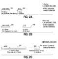
- FIGS. 2A and 2Bdetail data sectors 202 and their associated 9-bit math Reed-Solomon ECC code 204 , 206 of an embodiment of the present invention.
- the user datais stored in a 512-byte sector 202 that is concurrent with the ECC coverage area and is divided into 456 9-bit symbols for ECC purposes.
- the ECC code 204contains five 9-bit symbols stored in 6 bytes.
- the Reed-Solomon ECC encoding of the single data sector/ECC coverage area 202 and ECC code 204are designed to allow for the detection of 3 symbol errors and the correction of 2 symbol errors.
- this encodingincludes an additional error detection margin of 1 bit over the selected 2 bit correction ability to help foster predictable and stable operation of the ECC error correction (allowing the system to detect when it is in the situation of having more errors than it is capable of correcting, and to thus prevent operation of the ECC error correction in the situation where, instead of fixing errors, it would be potentially introducing more errors due to incorrect operation outside of its error correction range).
- the user datais also stored in a 512-byte sector 202 that is concurrent with the ECC coverage area and is divided into 456 9-bit symbols for ECC purposes.
- the ECC code 206contains ten 9-bit symbols stored in 12 bytes.
- the Reed-Solomon ECC encoding of the single data sector/ECC coverage area 202 and ECC code 206are designed to allow for the detection of 6 symbol errors and the correction of 4 symbol errors. It is noted that, while the ten 9-bit symbols allows an ECC detection range of 10 errors maximum or the ECC correction of 5 errors maximum, this encoding includes an additional error detection margin of 2 bits over the selected 4 bit correction ability to help foster predictable and stable operation of the ECC error correction.
- the additional coding ability of the ten symbol ECC check byte code over that of the five symbol ECC check byte codethus allows for an increase in the resulting error detection and correction ability.
- FIG. 2Cdetails an embodiment of the present invention having a generalized ECC coverage area 232 storing Y-bytes of user data divided into Z ECC symbols using X-bit math and protected by an associated X-bit math BCH ECC check byte code 234 that has a variable size of M-bytes/N X-bit symbols.
- the variable size of M-bytes/N X-bit symbols of the ECC code 234 of the generalized ECC coverage area 232allows for the detection/correction depth of the detection of J symbol errors and the correction of K symbol errors to be selected.
- ECC coverage areas sizes/math bases, ECC encoding schemes and ECC check byte code sizes of FIGS. 2A , 2 B, and 2 C incorporating embodiments of the present inventionwill be apparent to those skilled in the art with the benefit of the present disclosure.
- FIGS. 3A and 3Bdetail 9-bit Reed-Solomon ECC generators/encoders of an embodiment of the present invention.
- a 10-Symbol Reed-Solomon ECC encoder/LFSR 300is detailed.
- a 5-Symbol Reed-Solomon ECC encoder/LFSR 310is detailed. It is noted that the 5-Symbol Reed-Solomon ECC encoder 310 differs from the 10-Symbol Reed-Solomon ECC encoder 300 in that a different feedback path and coefficients are utilized for the smaller number of ECC check byte codes in the 5-Symbol encoder.
- 5-Symbol Reed-Solomon ECC encoder 310 and the 5-Symbol Reed-Solomon ECC encoder 300are detailed as separate circuits, a single 5 or 10-Symbol Reed-Solomon ECC encoder can be implemented that has a selectable feedback path and selectable or loadable polynomial coefficients to allow generation of either a 5 or 10-Symbol Reed-Solomon ECC check byte codes for data that is to be written to an associated memory.
- FIG. 3Cdetails a simplified flowchart of a Reed-Solomon ECC decoder 320 (also known as an ECC Checker/ECC Syndrome Generator) of an embodiment of the present invention utilizing 9-bit math and 5 or 10 symbol ECC check byte codes.
- the sector data and ECC check bytes 322(5 or 10 symbol based) are read in by the Reed-Solomon ECC decoder 320 and syndromes generated in the Syndrome Generator 324 from the sector data to check for errors, if the generated syndromes are zero, there is no error in the read sector data.
- the Syndrome Generator 340shown in FIG.
- Reed-Solomon syndrome generationis not dependent on the number of symbols utilized in the ECC check byte code and thus the same Syndrome Generator 340 can be utilized for both 5 symbol and 10 symbol ECC check byte codes.
- the Reed-Solomon ECC decoder 320executes the Berlekamp algorithm 326 to generate the error location polynomial (ELP).
- ELPerror location polynomial
- the Berlekamp algorithmshould be designed for the largest number of ECC check byte symbols that can be utilized (10 symbols in the case of the Reed-Solomon ECC decoder 320 of FIG. 3C ) the loop counters are then adjusted for the actual number of symbols being utilized.
- the Chien search 328is then implemented in the Reed-Solomon ECC decoder 320 utilizing the generated ELP polynomial to locate the actual error locations by iteratively looping through each of the possible error locations of the data to check to see if each is a solution 330 to the error polynomial, if the location is a solution to the ELP it is a data error.
- the Chien search 328is an iterative walk through the data to find solutions 330 to the ELP error polynomial it does not generally have to be adjusted for the number of ECC symbols being utilized in the ECC error correction, except for having to pad the input to the Chien search 328 with zeros for the unused symbols.
- FIG. 4shows a simplified diagram of a memory controller output 400 of an embodiment of the present invention coupled through a memory interface 402 to one or more Flash memory devices and through a host interface 404 to an external host (not shown), which typically is a processor or computer system.
- a data buffer 406is coupled to serially receive and hold a selected data block that is serially read through the memory interface 402 from a selected Flash memory device before it is transferred from the data buffer 406 through the host interface 404 under control of the host transfer hardware 414 .
- the serially streamed data blockis also coupled to a Reed-Solomon ECC checker/syndrome generator hardware 408 , which generates the syndromes from the data block and the stored ECC codes to see if they are non-zero, indicating that there is a data error.
- the Reed-Solomon ECC checker/syndrome generator hardware 408signals 410 to the host transfer hardware 414 to start the data transfer if the data block is correct (the ECC syndromes have been generated and evaluated correctly from the stored ECC codes and the data block, typically generating a string of zeros from the Reed-Solomon ECC syndrome generation hardware 408 ).
- the Reed-Solomon ECC checker/syndrome generator hardware 408signals 412 a (typically internal) microprocessor or dedicated ECC correction hardware 416 to correct the errors by utilizing a Reed-Solomon ECC correction algorithm.
- the microprocessor 416solves the Reed-Solomon ECC correction algorithm, using the generated syndromes to generate the error location polynomial (ELP) from the Berlekamp algorithm, and executing a Chien search using the generated ELP to determine the location of the bits to be corrected in the data block and applying the correction 418 to the data block contents held in the data buffer 406 .
- the microprocessor 416signals 420 the host transfer hardware 414 to begin transferring the data block from the data buffer 406 out through the host interface 404 .
- memory controller 400is designed to be externally coupled to one or more Flash memory devices
- memory outputs that are internal to a memory device incorporating embodiments of the present inventionshould be apparent to those skilled in the art with the benefit of the present disclosure. It is also noted that other embodiments incorporating differing ECC code schemes and math bases are also possible and should be apparent to those skilled in the art with the benefit of the present disclosure.
- the software routines that operate computer-based devicesare often stored on a variety of machine-usable or computer-usable storage mediums.
- These software routines and driversare often also referred to as firmware or ROM after the non-volatile ROM machine-usable storage device that such routines have historically been stored in.
- storage mediumscan include, but are not limited to, a non-volatile Flash memory, a ROM, an EEPROM, a one time programmable (OTP) device, a complex programmable logic device (CPLD), an application specific integrated circuit (ASIC), a magnetic media disk, etc.
- FIG. 5Ais a simplified diagram of a system 500 that incorporates a Flash memory device 504 embodiment of the present invention.
- the Flash memory 504is coupled to a processor 502 with an address/data bus 506 .
- a control state machine 510directs internal operation of the Flash memory device; managing the Flash memory array 508 and updating RAM control registers and tables 514 .
- the Flash memory array 508contains floating gate memory cells arranged in a sequence of erase blocks 516 , 518 .
- Each erase block 516 , 518contains a series of physical pages, each page containing one or more logical sectors 524 (shown here for illustration purposes as a single logical sector 524 per physical page/row) that contain a user data space 520 and a control/overhead data space 522 .
- the overhead data space 522contains overhead information for operation of the sector 520 , such as an error correction code (not shown), status flags, or an erase block management data field area (not shown).
- the RAM control registers and tables 514are loaded at power up from the non-volatile erase block management registers and tables (not shown) by the control state machine 510 .
- the user data space 520 in each logical sector 524is typically 512 bytes long.
- the Flash memory 504contains ECC generation and checking hardware 512 incorporating embodiments of the present invention.
- FIG. 5Bis a simplified diagram of another system 550 that incorporates a Flash memory system 560 embodiment of the present invention.
- the Flash memory system 560such as a memory system or Flash memory card, is coupled to a processor 552 with an address 554 , control 556 , and data bus 558 .
- a memory controller 566Internal to the Flash memory system 560 , a memory controller 566 directs internal operation of the Flash memory system 560 ; managing the Flash memory devices 562 , directing data accesses, updating internal control registers and tables (not shown), and/or directing operation of other possible hardware systems (not shown) of the Flash memory system 560 .
- the memory controller 566has an internal ECC generation and checking hardware (not shown) that incorporates embodiments of the present invention.
- the memory controller 566may optionally incorporate a small local embedded processor to help manage the Flash memory system 560 .
- the memory controller 566is coupled to and controls one or more Flash memory devices 562 via an internal control bus 564 . It is noted that other architectures Flash memory systems 560 , external interfaces 554 , 556 , 558 , and manners of coupling the memory controller 566 to the Flash memory devices 562 , such as directly coupled individual control busses and signal lines, are possible and should be apparent to those skilled in the art with benefit of the present disclosure.
- the Flash memory devices 562each contain a sequence of erase blocks 516 , 518 in their internal memory arrays.
- Each erase block 516 , 518contains a series of physical pages, each physical page having one or more logical sectors 524 that contain a user data space 520 and a control/overhead data space 522 (shown here for illustration purposes as a single logical sector 524 per physical page/row).
- the overhead data space 522contains an ECC code (not shown) and other overhead information for operation of the logical sector 520 , such as status flags, or an erase block management data field area (not shown).
- Flash memory embodiments of the present inventioncan apply to other non-volatile memory types including, but not limited to, polymer memory, multi-level cells (MLC) storage, NOR Flash, NAND Flash, virtual ground, FeRAM, OUM, NROM, and MRAM and should be apparent to those skilled in the art with the benefit of the present invention.
- MLCmulti-level cells
- FIG. 6is an illustration of a memory module 600 in accordance with an embodiment of the present invention.
- Memory module 600is illustrated as a memory card, although the concepts discussed with reference to memory module 600 are applicable to other types of removable or portable memory, e.g., USB flash drives, and are intended to be within the scope of “memory module” as used herein.
- memory modulee.g., USB flash drives
- FIG. 6shows one example form factor, these concepts are applicable to other form factors as well.
- memory module 600will include a housing 605 (as depicted) to enclose one or more memory devices 610 , though such a housing is not essential to all devices or device applications. At least one memory device 610 is a non-volatile memory including circuits of or adapted to perform elements of methods of the present invention.
- the housing 605includes one or more contacts 615 for communication with a host device. Examples of host devices include digital cameras, digital recording and playback devices, PDAs, personal computers, memory card readers, interface hubs and the like.
- the contacts 615are in the form of a standardized interface. For example, with a USB flash drive, the contacts 615 might be in the form of a USB Type-A male connector. In general, however, contacts 615 provide an interface for passing control, address and/or data signals between the memory module 600 and a host having compatible receptors for the contacts 615 .
- the memory module 600may optionally include additional circuitry 620 which may be one or more integrated circuits and/or discrete components.
- the additional circuitry 620may include a memory controller for controlling access across multiple memory devices 610 and/or for providing a translation layer between an external host and a memory device 610 .
- a memory controllercould selectively couple an I/O connection (not shown in FIG. 6 ) of a memory device 610 to receive the appropriate signal at the appropriate I/O connection at the appropriate time or to provide the appropriate signal at the appropriate contact 615 at the appropriate time.
- the communication protocol between a host and the memory module 600may be different than what is required for access of a memory device 610 .
- a memory controllercould then translate the command sequences received from a host into the appropriate command sequences to achieve the desired access to the memory device 610 .
- Such translationmay further include changes in signal voltage levels in addition to command sequences.
- the additional circuitry 620may further include functionality unrelated to control of a memory device 610 such as logic functions as might be performed by an ASIC (application specific integrated circuit). Also, the additional circuitry 620 may include circuitry to restrict read or write access to the memory module 600 , such as password protection, biometrics or the like. The additional circuitry 620 may include circuitry to indicate a status of the memory module 600 . For example, the additional circuitry 620 may include functionality to determine whether power is being supplied to the memory module 600 and whether the memory module 600 is currently being accessed, and to display an indication of its status, such as a solid light while powered and a flashing light while being accessed. The additional circuitry 620 may further include passive devices, such as decoupling capacitors to help regulate power requirements within the memory module 600 .
- Memory devices, circuitry, and data methodshave been described that facilitate the detection and correction of data in memory controllers, memory systems, and/or non-volatile memory devices by allowing the number of ECC check bytes being utilized to be varied to increase or decrease the ECC check depth.
- the depth of the ECC coverage(the overall number of bit errors detectable and/or correctable in each sector by the stored ECC check bytes) to be selected based on the application (such as increased error correction or speed of access), the amount of available data storage for ECC check bytes in the overhead/spare area associated with the sector, the version of memory device or controller being utilized, or the number of errors being seen in the memory system, device, bank, erase block, or sector (the error incidence rate), while the base data size of the area covered by the ECC check bytes (typically one or more sectors) stays the same.
Landscapes
- Engineering & Computer Science (AREA)
- Theoretical Computer Science (AREA)
- Quality & Reliability (AREA)
- Physics & Mathematics (AREA)
- General Engineering & Computer Science (AREA)
- General Physics & Mathematics (AREA)
- Techniques For Improving Reliability Of Storages (AREA)
- Detection And Correction Of Errors (AREA)
- Error Detection And Correction (AREA)
Abstract
Description
Claims (63)
Priority Applications (4)
| Application Number | Priority Date | Filing Date | Title |
|---|---|---|---|
| US11/513,571US7739576B2 (en) | 2006-08-31 | 2006-08-31 | Variable strength ECC |
| US11/711,699US20080053597A1 (en) | 2006-08-31 | 2007-02-27 | Multilayer hose |
| US12/814,885US8566675B2 (en) | 2006-08-31 | 2010-06-14 | Data handling |
| US14/059,057US9262261B2 (en) | 2006-08-31 | 2013-10-21 | Memory devices facilitating differing depths of error detection and/or error correction coverage |
Applications Claiming Priority (1)
| Application Number | Priority Date | Filing Date | Title |
|---|---|---|---|
| US11/513,571US7739576B2 (en) | 2006-08-31 | 2006-08-31 | Variable strength ECC |
Related Child Applications (1)
| Application Number | Title | Priority Date | Filing Date |
|---|---|---|---|
| US12/814,885ContinuationUS8566675B2 (en) | 2006-08-31 | 2010-06-14 | Data handling |
Publications (2)
| Publication Number | Publication Date |
|---|---|
| US20080072120A1 US20080072120A1 (en) | 2008-03-20 |
| US7739576B2true US7739576B2 (en) | 2010-06-15 |
Family
ID=39190106
Family Applications (3)
| Application Number | Title | Priority Date | Filing Date |
|---|---|---|---|
| US11/513,571Active2028-10-28US7739576B2 (en) | 2006-08-31 | 2006-08-31 | Variable strength ECC |
| US12/814,885Active2027-09-12US8566675B2 (en) | 2006-08-31 | 2010-06-14 | Data handling |
| US14/059,057Active2026-09-17US9262261B2 (en) | 2006-08-31 | 2013-10-21 | Memory devices facilitating differing depths of error detection and/or error correction coverage |
Family Applications After (2)
| Application Number | Title | Priority Date | Filing Date |
|---|---|---|---|
| US12/814,885Active2027-09-12US8566675B2 (en) | 2006-08-31 | 2010-06-14 | Data handling |
| US14/059,057Active2026-09-17US9262261B2 (en) | 2006-08-31 | 2013-10-21 | Memory devices facilitating differing depths of error detection and/or error correction coverage |
Country Status (1)
| Country | Link |
|---|---|
| US (3) | US7739576B2 (en) |
Cited By (64)
| Publication number | Priority date | Publication date | Assignee | Title |
|---|---|---|---|---|
| US20080034270A1 (en)* | 2006-08-07 | 2008-02-07 | Fujitsu Limited | Semiconductor memory device capable of changing ECC code length |
| US20080168329A1 (en)* | 2007-01-04 | 2008-07-10 | Junsheng Han | Error control coding methods for memories with subline accesses |
| US20080195810A1 (en)* | 2007-02-09 | 2008-08-14 | Zining Wu | Nonvolatile memory system |
| US20080256415A1 (en)* | 2005-09-27 | 2008-10-16 | Nxp B.V. | Error Detection/Correction Circuit as Well as Corresponding Method |
| US20080276150A1 (en)* | 2007-05-02 | 2008-11-06 | Samsung Electronics Co., Ltd | Error control code apparatuses and methods of using the same |
| US20100251066A1 (en)* | 2006-08-31 | 2010-09-30 | Micron Technology, Inc. | Data handling |
| US20110047438A1 (en)* | 2008-04-02 | 2011-02-24 | Netac Technology Co., Ltd. | Computer and data storage method |
| US20110191654A1 (en)* | 2010-02-03 | 2011-08-04 | Seagate Technology Llc | Adjustable error correction code length in an electrical storage device |
| US20110213945A1 (en)* | 2010-02-26 | 2011-09-01 | Apple Inc. | Data partitioning scheme for non-volatile memories |
| WO2012058328A1 (en)* | 2010-10-27 | 2012-05-03 | Sandforce, Inc. | Adaptive ecc techniques for flash memory based data storage |
| US20130024735A1 (en)* | 2011-07-19 | 2013-01-24 | Ocz Technology Group Inc. | Solid-state memory-based storage method and device with low error rate |
| US8386895B2 (en) | 2010-05-19 | 2013-02-26 | Micron Technology, Inc. | Enhanced multilevel memory |
| US20130111295A1 (en)* | 2011-10-31 | 2013-05-02 | Sheng Li | Methods and apparatus to perform error detection and correction |
| US8489979B2 (en) | 2010-05-28 | 2013-07-16 | Seagate Technology Llc | Methods and devices to reduce outer code failure rate variability |
| US8572457B2 (en) | 2010-05-28 | 2013-10-29 | Seagate Technology Llc | Outer code protection for solid state memory devices |
| US8578248B2 (en)* | 2006-10-10 | 2013-11-05 | Marvell World Trade Ltd. | Adaptive systems and methods for storing and retrieving data to and from memory cells |
| US8656101B2 (en) | 2011-01-18 | 2014-02-18 | Lsi Corporation | Higher-level redundancy information computation |
| US20140068376A1 (en)* | 2012-08-30 | 2014-03-06 | Kabushiki Kaisha Toshiba | Memory controller and semiconductor storage device |
| US8719663B2 (en) | 2010-12-12 | 2014-05-06 | Lsi Corporation | Cross-decoding for non-volatile storage |
| US20140173377A1 (en)* | 2011-07-26 | 2014-06-19 | Kabushiki Kaisha Toshiba | Memory controller, semiconductor storage device, and decoding method |
| US8788910B1 (en) | 2012-05-22 | 2014-07-22 | Pmc-Sierra, Inc. | Systems and methods for low latency, high reliability error correction in a flash drive |
| US8793556B1 (en) | 2012-05-22 | 2014-07-29 | Pmc-Sierra, Inc. | Systems and methods for reclaiming flash blocks of a flash drive |
| US8856431B2 (en) | 2012-08-02 | 2014-10-07 | Lsi Corporation | Mixed granularity higher-level redundancy for non-volatile memory |
| US20140317447A1 (en)* | 2010-09-28 | 2014-10-23 | Pure Storage, Inc. | Adaptive raid for an ssd environment |
| US8898548B1 (en)* | 2012-08-24 | 2014-11-25 | Western Digital Technologies, Inc. | Methods, data storage devices and systems having variable size ECC page size |
| US8935595B2 (en) | 2010-03-12 | 2015-01-13 | Lsi Corporation | LDPC erasure decoding for flash memories |
| US8949686B1 (en) | 2011-02-13 | 2015-02-03 | Apple Inc. | Protection against word line failure in memory devices |
| US8972826B2 (en) | 2012-10-24 | 2015-03-03 | Western Digital Technologies, Inc. | Adaptive error correction codes for data storage systems |
| US8972824B1 (en)* | 2012-05-22 | 2015-03-03 | Pmc-Sierra, Inc. | Systems and methods for transparently varying error correction code strength in a flash drive |
| US8996957B1 (en) | 2012-05-22 | 2015-03-31 | Pmc-Sierra, Inc. | Systems and methods for initializing regions of a flash drive having diverse error correction coding (ECC) schemes |
| US9009562B2 (en) | 2013-01-30 | 2015-04-14 | Hewlett-Packard Development Company, L.P. | Providing memory protection using a modified error correction code |
| US9009565B1 (en) | 2013-03-15 | 2015-04-14 | Pmc-Sierra, Inc. | Systems and methods for mapping for solid-state memory |
| US9021336B1 (en) | 2012-05-22 | 2015-04-28 | Pmc-Sierra, Inc. | Systems and methods for redundantly storing error correction codes in a flash drive with secondary parity information spread out across each page of a group of pages |
| US9021339B2 (en) | 2012-11-29 | 2015-04-28 | Western Digital Technologies, Inc. | Data reliability schemes for data storage systems |
| US9021333B1 (en) | 2012-05-22 | 2015-04-28 | Pmc-Sierra, Inc. | Systems and methods for recovering data from failed portions of a flash drive |
| US9021337B1 (en) | 2012-05-22 | 2015-04-28 | Pmc-Sierra, Inc. | Systems and methods for adaptively selecting among different error correction coding schemes in a flash drive |
| US9026867B1 (en) | 2013-03-15 | 2015-05-05 | Pmc-Sierra, Inc. | Systems and methods for adapting to changing characteristics of multi-level cells in solid-state memory |
| US9047214B1 (en) | 2012-05-22 | 2015-06-02 | Pmc-Sierra, Inc. | System and method for tolerating a failed page in a flash device |
| US9053012B1 (en) | 2013-03-15 | 2015-06-09 | Pmc-Sierra, Inc. | Systems and methods for storing data for solid-state memory |
| US9059736B2 (en) | 2012-12-03 | 2015-06-16 | Western Digital Technologies, Inc. | Methods, solid state drive controllers and data storage devices having a runtime variable raid protection scheme |
| US9081701B1 (en) | 2013-03-15 | 2015-07-14 | Pmc-Sierra, Inc. | Systems and methods for decoding data for solid-state memory |
| US9105305B2 (en) | 2010-12-01 | 2015-08-11 | Seagate Technology Llc | Dynamic higher-level redundancy mode management with independent silicon elements |
| US9176812B1 (en) | 2012-05-22 | 2015-11-03 | Pmc-Sierra, Inc. | Systems and methods for storing data in page stripes of a flash drive |
| US9183085B1 (en) | 2012-05-22 | 2015-11-10 | Pmc-Sierra, Inc. | Systems and methods for adaptively selecting from among a plurality of error correction coding schemes in a flash drive for robustness and low latency |
| US9201728B2 (en) | 2013-09-12 | 2015-12-01 | Seagate Technology Llc | Memory device with variable code rate |
| US20150350082A1 (en)* | 2014-06-02 | 2015-12-03 | Micron Technology, Inc. | Systems and methods for throttling packet transmission in a scalable memory system protocol |
| US9208018B1 (en) | 2013-03-15 | 2015-12-08 | Pmc-Sierra, Inc. | Systems and methods for reclaiming memory for solid-state memory |
| US9214963B1 (en) | 2012-12-21 | 2015-12-15 | Western Digital Technologies, Inc. | Method and system for monitoring data channel to enable use of dynamically adjustable LDPC coding parameters in a data storage system |
| US9235468B2 (en) | 2013-04-12 | 2016-01-12 | Qualcomm Incorporated | Systems and methods to improve the reliability and lifespan of flash memory |
| US9529653B2 (en) | 2014-10-09 | 2016-12-27 | International Business Machines Corporation | Processor register error correction management |
| US9559725B1 (en) | 2013-10-23 | 2017-01-31 | Seagate Technology Llc | Multi-strength reed-solomon outer code protection |
| US9577673B2 (en) | 2012-11-08 | 2017-02-21 | Micron Technology, Inc. | Error correction methods and apparatuses using first and second decoders |
| US9646718B2 (en) | 2014-08-01 | 2017-05-09 | Samsung Electronics Co., Ltd. | Semiconductor memory device having selective ECC function |
| US20170177432A1 (en)* | 2015-12-22 | 2017-06-22 | Freescale Semiconductor, Inc. | Memory controller and method of operating a memory controller |
| US20170220411A1 (en)* | 2009-12-29 | 2017-08-03 | Micron Technology, Inc. | Memory device having address and command selectable capabilities |
| US9727414B2 (en) | 2010-12-01 | 2017-08-08 | Seagate Technology Llc | Fractional redundant array of silicon independent elements |
| US10067823B2 (en) | 2014-12-04 | 2018-09-04 | Western Digital Technologies, Inc. | Systems and methods for adaptive error corrective code mechanisms |
| US10284231B2 (en) | 2017-06-01 | 2019-05-07 | Seagate Technology, Llc | Adaptive outer code for consistent overprovisioning (OP) level |
| US10409675B2 (en)* | 2015-01-08 | 2019-09-10 | Micron Technology, Inc. | Semiconductor device having error correction code (ECC) circuit |
| US10452472B1 (en) | 2018-06-04 | 2019-10-22 | Hewlett Packard Enterprise Development Lp | Tunable and dynamically adjustable error correction for memristor crossbars |
| US10896002B2 (en) | 2018-06-29 | 2021-01-19 | Seagate Technology Llc | Reverse directory structure in a garbage collection unit (GCU) |
| US11138069B2 (en) | 2018-06-11 | 2021-10-05 | Seagate Technology, Llc | Providing additional parity for non-standard sized parity data sets |
| US11150984B2 (en) | 2014-12-04 | 2021-10-19 | Western Digital Technologies, Inc. | Systems and methods for multi-zone data tiering for endurance extension in solid state drives |
| US20230289259A1 (en)* | 2022-03-08 | 2023-09-14 | SK Hynix Inc. | Memory and operation method of the same |
Families Citing this family (155)
| Publication number | Priority date | Publication date | Assignee | Title |
|---|---|---|---|---|
| US7904780B2 (en)* | 2006-11-03 | 2011-03-08 | Sandisk Corporation | Methods of modulating error correction coding |
| US8001441B2 (en)* | 2006-11-03 | 2011-08-16 | Sandisk Technologies Inc. | Nonvolatile memory with modulated error correction coding |
| DE102007011801B4 (en)* | 2007-03-12 | 2009-04-02 | Qimonda Ag | Circuit for generating an error coding data block, device with the circuit, device for generating an error coding data block |
| US7958301B2 (en)* | 2007-04-10 | 2011-06-07 | Marvell World Trade Ltd. | Memory controller and method for memory pages with dynamically configurable bits per cell |
| US20080288712A1 (en)* | 2007-04-25 | 2008-11-20 | Cornwell Michael J | Accessing metadata with an external host |
| JP2008287404A (en)* | 2007-05-16 | 2008-11-27 | Hitachi Ltd | Apparatus and method for detecting and recovering data corruption of non-access memory cell due to reading |
| US8583857B2 (en)* | 2007-08-20 | 2013-11-12 | Marvell World Trade Ltd. | Method and system for object-oriented data storage |
| US20090055605A1 (en)* | 2007-08-20 | 2009-02-26 | Zining Wu | Method and system for object-oriented data storage |
| JP4564520B2 (en) | 2007-08-31 | 2010-10-20 | 株式会社東芝 | Semiconductor memory device and control method thereof |
| US20090070655A1 (en)* | 2007-09-11 | 2009-03-12 | Silicon Motion, Inc. | Method for Generating an ECC Code for a Memory Device |
| US8650352B2 (en) | 2007-09-20 | 2014-02-11 | Densbits Technologies Ltd. | Systems and methods for determining logical values of coupled flash memory cells |
| US8365040B2 (en) | 2007-09-20 | 2013-01-29 | Densbits Technologies Ltd. | Systems and methods for handling immediate data errors in flash memory |
| US8694715B2 (en) | 2007-10-22 | 2014-04-08 | Densbits Technologies Ltd. | Methods for adaptively programming flash memory devices and flash memory systems incorporating same |
| KR101437517B1 (en)* | 2007-10-23 | 2014-09-05 | 삼성전자주식회사 | Memory system using interleaving technique, and method thereof |
| US8443242B2 (en)* | 2007-10-25 | 2013-05-14 | Densbits Technologies Ltd. | Systems and methods for multiple coding rates in flash devices |
| US20090125790A1 (en)* | 2007-11-13 | 2009-05-14 | Mcm Portfolio Llc | Method and Apparatus of Automatically Selecting Error Correction Algorithms by a NAND Flash Controller |
| JP2009129070A (en)* | 2007-11-21 | 2009-06-11 | Hitachi Ltd | Control method of flash memory storage device, flash memory storage device and storage system using the method |
| US8321625B2 (en) | 2007-12-05 | 2012-11-27 | Densbits Technologies Ltd. | Flash memory device with physical cell value deterioration accommodation and methods useful in conjunction therewith |
| WO2009072105A2 (en) | 2007-12-05 | 2009-06-11 | Densbits Technologies Ltd. | A low power chien-search based bch/rs decoding system for flash memory, mobile communications devices and other applications |
| US8335977B2 (en) | 2007-12-05 | 2012-12-18 | Densbits Technologies Ltd. | Flash memory apparatus and methods using a plurality of decoding stages including optional use of concatenated BCH codes and/or designation of “first below” cells |
| US8359516B2 (en) | 2007-12-12 | 2013-01-22 | Densbits Technologies Ltd. | Systems and methods for error correction and decoding on multi-level physical media |
| US8276051B2 (en)* | 2007-12-12 | 2012-09-25 | Densbits Technologies Ltd. | Chien-search system employing a clock-gating scheme to save power for error correction decoder and other applications |
| US8327246B2 (en) | 2007-12-18 | 2012-12-04 | Densbits Technologies Ltd. | Apparatus for coding at a plurality of rates in multi-level flash memory systems, and methods useful in conjunction therewith |
| WO2009118720A2 (en) | 2008-03-25 | 2009-10-01 | Densbits Technologies Ltd. | Apparatus and methods for hardware-efficient unbiased rounding |
| US9477587B2 (en) | 2008-04-11 | 2016-10-25 | Micron Technology, Inc. | Method and apparatus for a volume management system in a non-volatile memory device |
| US8627169B2 (en)* | 2008-06-20 | 2014-01-07 | Cadence Design Systems, Inc. | Method and apparatus for dynamically configurable multi level error correction |
| US8332725B2 (en) | 2008-08-20 | 2012-12-11 | Densbits Technologies Ltd. | Reprogramming non volatile memory portions |
| US8296620B2 (en)* | 2008-08-26 | 2012-10-23 | Seagate Technology Llc | Data devices including multiple error correction codes and methods of utilizing |
| TWI393146B (en)* | 2008-10-15 | 2013-04-11 | Genesys Logic Inc | Flash memory controller having configuring unit of error correction code (ecc) capability and method thereof |
| US8161354B2 (en)* | 2008-10-16 | 2012-04-17 | Genesys Logic, Inc. | Flash memory controller having configuring unit for error correction code (ECC) capability and method thereof |
| KR20100050789A (en)* | 2008-11-06 | 2010-05-14 | 삼성전자주식회사 | Memory device and memory system including the same |
| US8156411B2 (en) | 2008-11-06 | 2012-04-10 | Freescale Semiconductor, Inc. | Error correction of an encoded message |
| US7843660B1 (en)* | 2008-11-25 | 2010-11-30 | Western Digital Technologies, Inc. | Disk drive adjusting erasure window based on a number of non-read data sectors during a retry operation |
| US8555143B2 (en)* | 2008-12-22 | 2013-10-08 | Industrial Technology Research Institute | Flash memory controller and the method thereof |
| US8473815B2 (en)* | 2008-12-22 | 2013-06-25 | Industrial Technology Research Institute | Methods and systems of a flash memory controller and an error correction code (ECC) controller using variable-length segmented ECC data |
| JP5458568B2 (en)* | 2008-12-25 | 2014-04-02 | ソニー株式会社 | Nonvolatile storage device, information recording system, and information recording method |
| KR101042197B1 (en)* | 2008-12-30 | 2011-06-20 | (주)인디링스 | Memory Controllers and Memory Management Methods |
| KR20100102925A (en)* | 2009-03-12 | 2010-09-27 | 삼성전자주식회사 | Non-volatile memory device and memory system generating read reclaim signal |
| US8418021B2 (en)* | 2009-03-27 | 2013-04-09 | Mediatek Inc. | Storage controller with encoding/decoding circuit programmable to support different ECC requirements and related method thereof |
| US8819385B2 (en) | 2009-04-06 | 2014-08-26 | Densbits Technologies Ltd. | Device and method for managing a flash memory |
| US8458574B2 (en) | 2009-04-06 | 2013-06-04 | Densbits Technologies Ltd. | Compact chien-search based decoding apparatus and method |
| KR101572879B1 (en)* | 2009-04-29 | 2015-12-01 | 삼성전자주식회사 | Systems and methods for dynamically parallelizing parallel applications |
| US8566510B2 (en) | 2009-05-12 | 2013-10-22 | Densbits Technologies Ltd. | Systems and method for flash memory management |
| US8054691B2 (en) | 2009-06-26 | 2011-11-08 | Sandisk Technologies Inc. | Detecting the completion of programming for non-volatile storage |
| TWI508089B (en)* | 2009-06-29 | 2015-11-11 | A Data Technology Co Ltd | An electronic memory device and correction operation method thereof |
| KR101062755B1 (en)* | 2009-07-29 | 2011-09-06 | 주식회사 하이닉스반도체 | Semiconductor memory system including ECC circuit and control method thereof |
| EP2299362A3 (en)* | 2009-08-18 | 2011-05-04 | ViaSat, Inc. | Forward error correction for memories |
| US8077515B2 (en) | 2009-08-25 | 2011-12-13 | Micron Technology, Inc. | Methods, devices, and systems for dealing with threshold voltage change in memory devices |
| US8995197B1 (en) | 2009-08-26 | 2015-03-31 | Densbits Technologies Ltd. | System and methods for dynamic erase and program control for flash memory device memories |
| US9330767B1 (en) | 2009-08-26 | 2016-05-03 | Avago Technologies General Ip (Singapore) Pte. Ltd. | Flash memory module and method for programming a page of flash memory cells |
| US8868821B2 (en) | 2009-08-26 | 2014-10-21 | Densbits Technologies Ltd. | Systems and methods for pre-equalization and code design for a flash memory |
| US8305812B2 (en) | 2009-08-26 | 2012-11-06 | Densbits Technologies Ltd. | Flash memory module and method for programming a page of flash memory cells |
| US8271697B2 (en) | 2009-09-29 | 2012-09-18 | Micron Technology, Inc. | State change in systems having devices coupled in a chained configuration |
| US8730729B2 (en) | 2009-10-15 | 2014-05-20 | Densbits Technologies Ltd. | Systems and methods for averaging error rates in non-volatile devices and storage systems |
| US8724387B2 (en) | 2009-10-22 | 2014-05-13 | Densbits Technologies Ltd. | Method, system, and computer readable medium for reading and programming flash memory cells using multiple bias voltages |
| US8626988B2 (en) | 2009-11-19 | 2014-01-07 | Densbits Technologies Ltd. | System and method for uncoded bit error rate equalization via interleaving |
| US9037777B2 (en) | 2009-12-22 | 2015-05-19 | Densbits Technologies Ltd. | Device, system, and method for reducing program/read disturb in flash arrays |
| US8607124B2 (en) | 2009-12-24 | 2013-12-10 | Densbits Technologies Ltd. | System and method for setting a flash memory cell read threshold |
| CN102110028A (en)* | 2009-12-25 | 2011-06-29 | 康佳集团股份有限公司 | NAND flash memory as well as data checking method and device thereof |
| US8341502B2 (en) | 2010-02-28 | 2012-12-25 | Densbits Technologies Ltd. | System and method for multi-dimensional decoding |
| US8516274B2 (en) | 2010-04-06 | 2013-08-20 | Densbits Technologies Ltd. | Method, system and medium for analog encryption in a flash memory |
| US8527840B2 (en) | 2010-04-06 | 2013-09-03 | Densbits Technologies Ltd. | System and method for restoring damaged data programmed on a flash device |
| US8745317B2 (en) | 2010-04-07 | 2014-06-03 | Densbits Technologies Ltd. | System and method for storing information in a multi-level cell memory |
| US8429391B2 (en) | 2010-04-16 | 2013-04-23 | Micron Technology, Inc. | Boot partitions in memory devices and systems |
| JP5574230B2 (en)* | 2010-04-28 | 2014-08-20 | 株式会社日立製作所 | Fault handling method and computer |
| US9021177B2 (en) | 2010-04-29 | 2015-04-28 | Densbits Technologies Ltd. | System and method for allocating and using spare blocks in a flash memory |
| US8451664B2 (en) | 2010-05-12 | 2013-05-28 | Micron Technology, Inc. | Determining and using soft data in memory devices and systems |
| WO2011159806A2 (en)* | 2010-06-15 | 2011-12-22 | Fusion-Io, Inc. | Apparatus, system, and method for providing error correction |
| US8468431B2 (en) | 2010-07-01 | 2013-06-18 | Densbits Technologies Ltd. | System and method for multi-dimensional encoding and decoding |
| US8539311B2 (en) | 2010-07-01 | 2013-09-17 | Densbits Technologies Ltd. | System and method for data recovery in multi-level cell memories |
| US20120008414A1 (en) | 2010-07-06 | 2012-01-12 | Michael Katz | Systems and methods for storing, retrieving, and adjusting read thresholds in flash memory storage system |
| TWI455144B (en)* | 2010-07-22 | 2014-10-01 | Silicon Motion Inc | Controlling methods and controllers utilized in flash memory device |
| US8964464B2 (en) | 2010-08-24 | 2015-02-24 | Densbits Technologies Ltd. | System and method for accelerated sampling |
| US8508995B2 (en) | 2010-09-15 | 2013-08-13 | Densbits Technologies Ltd. | System and method for adjusting read voltage thresholds in memories |
| US20120254686A1 (en)* | 2010-10-01 | 2012-10-04 | SIGLEAD Inc. | Non-volatile semiconductor memory devices and error correction methods |
| CN102456400B (en)* | 2010-10-15 | 2015-03-11 | 慧荣科技股份有限公司 | Control method and controller for flash memory |
| US9063878B2 (en) | 2010-11-03 | 2015-06-23 | Densbits Technologies Ltd. | Method, system and computer readable medium for copy back |
| US8850100B2 (en) | 2010-12-07 | 2014-09-30 | Densbits Technologies Ltd. | Interleaving codeword portions between multiple planes and/or dies of a flash memory device |
| US10079068B2 (en) | 2011-02-23 | 2018-09-18 | Avago Technologies General Ip (Singapore) Pte. Ltd. | Devices and method for wear estimation based memory management |
| US8693258B2 (en) | 2011-03-17 | 2014-04-08 | Densbits Technologies Ltd. | Obtaining soft information using a hard interface |
| CN102693760B (en)* | 2011-03-24 | 2015-07-15 | 扬智科技股份有限公司 | Error Correction Method for NAND Flash Memory |
| US8990665B1 (en) | 2011-04-06 | 2015-03-24 | Densbits Technologies Ltd. | System, method and computer program product for joint search of a read threshold and soft decoding |
| US8799745B2 (en)* | 2011-04-12 | 2014-08-05 | Hitachi, Ltd. | Storage control apparatus and error correction method |
| US9372792B1 (en) | 2011-05-12 | 2016-06-21 | Avago Technologies General Ip (Singapore) Pte. Ltd. | Advanced management of a non-volatile memory |
| US9501392B1 (en) | 2011-05-12 | 2016-11-22 | Avago Technologies General Ip (Singapore) Pte. Ltd. | Management of a non-volatile memory module |
| US8996790B1 (en) | 2011-05-12 | 2015-03-31 | Densbits Technologies Ltd. | System and method for flash memory management |
| US9110785B1 (en) | 2011-05-12 | 2015-08-18 | Densbits Technologies Ltd. | Ordered merge of data sectors that belong to memory space portions |
| US9195592B1 (en) | 2011-05-12 | 2015-11-24 | Densbits Technologies Ltd. | Advanced management of a non-volatile memory |
| US9396106B2 (en) | 2011-05-12 | 2016-07-19 | Avago Technologies General Ip (Singapore) Pte. Ltd. | Advanced management of a non-volatile memory |
| US8667211B2 (en) | 2011-06-01 | 2014-03-04 | Densbits Technologies Ltd. | System and method for managing a non-volatile memory |
| US8572466B2 (en) | 2011-06-06 | 2013-10-29 | Micron Technology, Inc. | Apparatuses, systems, devices, and methods of replacing at least partially non-functional portions of memory |
| US8588003B1 (en) | 2011-08-01 | 2013-11-19 | Densbits Technologies Ltd. | System, method and computer program product for programming and for recovering from a power failure |
| US8902653B2 (en) | 2011-08-12 | 2014-12-02 | Micron Technology, Inc. | Memory devices and configuration methods for a memory device |
| US8553468B2 (en) | 2011-09-21 | 2013-10-08 | Densbits Technologies Ltd. | System and method for managing erase operations in a non-volatile memory |
| US9753858B2 (en) | 2011-11-30 | 2017-09-05 | Advanced Micro Devices, Inc. | DRAM cache with tags and data jointly stored in physical rows |
| US8996788B2 (en) | 2012-02-09 | 2015-03-31 | Densbits Technologies Ltd. | Configurable flash interface |
| US8947941B2 (en) | 2012-02-09 | 2015-02-03 | Densbits Technologies Ltd. | State responsive operations relating to flash memory cells |
| TW201337936A (en)* | 2012-03-06 | 2013-09-16 | Innodisk Corp | Flash memory device capable of raising data correction capability |
| US8996793B1 (en) | 2012-04-24 | 2015-03-31 | Densbits Technologies Ltd. | System, method and computer readable medium for generating soft information |
| US8838937B1 (en) | 2012-05-23 | 2014-09-16 | Densbits Technologies Ltd. | Methods, systems and computer readable medium for writing and reading data |
| US8879325B1 (en) | 2012-05-30 | 2014-11-04 | Densbits Technologies Ltd. | System, method and computer program product for processing read threshold information and for reading a flash memory module |
| TWI594254B (en)* | 2012-07-17 | 2017-08-01 | 慧榮科技股份有限公司 | Method for reading data from block of flash memory and associated memory device |
| US9921954B1 (en) | 2012-08-27 | 2018-03-20 | Avago Technologies General Ip (Singapore) Pte. Ltd. | Method and system for split flash memory management between host and storage controller |
| US8984368B2 (en)* | 2012-10-11 | 2015-03-17 | Advanced Micro Devices, Inc. | High reliability memory controller |
| JP5997577B2 (en)* | 2012-10-18 | 2016-09-28 | オークマ株式会社 | Chatter vibration suppressing method and machine tool |
| US9368225B1 (en) | 2012-11-21 | 2016-06-14 | Avago Technologies General Ip (Singapore) Pte. Ltd. | Determining read thresholds based upon read error direction statistics |
| US9069659B1 (en) | 2013-01-03 | 2015-06-30 | Densbits Technologies Ltd. | Read threshold determination using reference read threshold |
| US11416340B1 (en)* | 2013-01-04 | 2022-08-16 | Pure Storage, Inc. | Storage system with multiple storage types in a vast storage network |
| WO2014120660A1 (en) | 2013-01-29 | 2014-08-07 | Marvell World Trade Ltd. | Methods and apparatus for storing data to a solid state storage device based on data classification |
| US20140229655A1 (en)* | 2013-02-08 | 2014-08-14 | Seagate Technology Llc | Storing Error Correction Code (ECC) Data In a Multi-Tier Memory Structure |
| KR102102171B1 (en)* | 2013-04-05 | 2020-05-29 | 삼성전자 주식회사 | Multi level cell memory system |
| US9136876B1 (en) | 2013-06-13 | 2015-09-15 | Densbits Technologies Ltd. | Size limited multi-dimensional decoding |
| CN103412778A (en)* | 2013-08-12 | 2013-11-27 | 上海盈方微电子股份有限公司 | Program boot method and device of SOC (system on a chip) NAND Flash memory |
| US20150058697A1 (en)* | 2013-08-22 | 2015-02-26 | Kabushiki Kaisha Toshiba | Storage device, controller and memory controlling method |
| US9413491B1 (en) | 2013-10-08 | 2016-08-09 | Avago Technologies General Ip (Singapore) Pte. Ltd. | System and method for multiple dimension decoding and encoding a message |
| US9348694B1 (en) | 2013-10-09 | 2016-05-24 | Avago Technologies General Ip (Singapore) Pte. Ltd. | Detecting and managing bad columns |
| US9786388B1 (en) | 2013-10-09 | 2017-10-10 | Avago Technologies General Ip (Singapore) Pte. Ltd. | Detecting and managing bad columns |
| US9397706B1 (en) | 2013-10-09 | 2016-07-19 | Avago Technologies General Ip (Singapore) Pte. Ltd. | System and method for irregular multiple dimension decoding and encoding |
| KR102085127B1 (en)* | 2013-11-13 | 2020-04-14 | 삼성전자주식회사 | the method of memory controller operation and the non volatile memory device under the control of the memory controller |
| US9323609B2 (en)* | 2013-11-15 | 2016-04-26 | Intel Corporation | Data storage and variable length error correction information |
| JP2015106872A (en)* | 2013-12-02 | 2015-06-08 | ソニー株式会社 | Error correction device, error correction method, and program |
| CN103778030B (en)* | 2013-12-30 | 2017-09-22 | 上海晨思电子科技有限公司 | Daily record subsystem wiring method, error tracking method and processor |
| US9536612B1 (en) | 2014-01-23 | 2017-01-03 | Avago Technologies General Ip (Singapore) Pte. Ltd | Digital signaling processing for three dimensional flash memory arrays |
| US10120792B1 (en) | 2014-01-29 | 2018-11-06 | Avago Technologies General Ip (Singapore) Pte. Ltd. | Programming an embedded flash storage device |
| KR20150090414A (en)* | 2014-01-29 | 2015-08-06 | 에스케이하이닉스 주식회사 | Semicondcutor device performing error correction |
| CN103744744B (en)* | 2014-02-08 | 2017-08-25 | 威盛电子股份有限公司 | Data storage device and data verification method of volatile memory |
| CN103777904B (en) | 2014-02-12 | 2017-07-21 | 威盛电子股份有限公司 | Data storage device and data scrambling and descrambling method |
| US9954557B2 (en)* | 2014-04-30 | 2018-04-24 | Microsoft Technology Licensing, Llc | Variable width error correction |
| US9542262B1 (en) | 2014-05-29 | 2017-01-10 | Avago Technologies General Ip (Singapore) Pte. Ltd. | Error correction |
| US10116336B2 (en)* | 2014-06-13 | 2018-10-30 | Sandisk Technologies Llc | Error correcting code adjustment for a data storage device |
| US9442787B2 (en)* | 2014-06-13 | 2016-09-13 | Sandisk Technologies Llc | Three dimensional (3D) memory including error detection circuitry |
| US9892033B1 (en) | 2014-06-24 | 2018-02-13 | Avago Technologies General Ip (Singapore) Pte. Ltd. | Management of memory units |
| US9972393B1 (en) | 2014-07-03 | 2018-05-15 | Avago Technologies General Ip (Singapore) Pte. Ltd. | Accelerating programming of a flash memory module |
| US9584159B1 (en) | 2014-07-03 | 2017-02-28 | Avago Technologies General Ip (Singapore) Pte. Ltd. | Interleaved encoding |
| US9449702B1 (en) | 2014-07-08 | 2016-09-20 | Avago Technologies General Ip (Singapore) Pte. Ltd. | Power management |
| US9524211B1 (en) | 2014-11-18 | 2016-12-20 | Avago Technologies General Ip (Singapore) Pte. Ltd. | Codeword management |
| US9654148B2 (en)* | 2015-01-06 | 2017-05-16 | Samsung Electronics Co., Ltd. | Reconfigurable ECC for memory |
| US10305515B1 (en) | 2015-02-02 | 2019-05-28 | Avago Technologies International Sales Pte. Limited | System and method for encoding using multiple linear feedback shift registers |
| US10141955B2 (en)* | 2015-04-11 | 2018-11-27 | International Business Machines Corporation | Method and apparatus for selective and power-aware memory error protection and memory management |
| US10628255B1 (en) | 2015-06-11 | 2020-04-21 | Avago Technologies International Sales Pte. Limited | Multi-dimensional decoding |
| US9851921B1 (en) | 2015-07-05 | 2017-12-26 | Avago Technologies General Ip (Singapore) Pte. Ltd. | Flash memory chip processing |
| US9817714B2 (en)* | 2015-08-28 | 2017-11-14 | Intel Corporation | Memory device on-die error checking and correcting code |
| JP6158265B2 (en)* | 2015-09-16 | 2017-07-05 | 株式会社東芝 | Cache memory system |
| CN107015880B (en)* | 2016-01-28 | 2020-06-30 | 京微雅格(北京)科技有限公司 | FPGA circuit and configuration file processing method thereof |
| US9954558B1 (en) | 2016-03-03 | 2018-04-24 | Avago Technologies General Ip (Singapore) Pte. Ltd. | Fast decoding of data stored in a flash memory |
| JP2018156463A (en)* | 2017-03-17 | 2018-10-04 | 東芝メモリ株式会社 | Memory system |
| JP2019121129A (en)* | 2017-12-28 | 2019-07-22 | 株式会社日立製作所 | Non-volatile memory |
| US11314425B2 (en) | 2018-05-08 | 2022-04-26 | Micron Technology, Inc. | Read error recovery |
| CN111771192A (en) | 2018-05-11 | 2020-10-13 | 拉姆伯斯公司 | Efficient Storage of Error Correcting Code Information |
| US10691532B2 (en)* | 2018-06-29 | 2020-06-23 | Alibaba Group Holding Limited | Storage drive error-correcting code-assisted scrubbing for dynamic random-access memory retention time handling |
| US11042432B1 (en)* | 2019-12-20 | 2021-06-22 | Western Digital Technologies, Inc. | Data storage device with dynamic stripe length manager |
| US11537292B2 (en)* | 2020-06-24 | 2022-12-27 | Western Digital Technologies, Inc. | Methods and apparatus for enhancing uber rate for storage devices |
| WO2022139848A1 (en)* | 2020-12-26 | 2022-06-30 | Intel Corporation | Dynamic hardware integrity and/or replay protection |
| CN114816807B (en)* | 2021-01-22 | 2025-07-25 | 南宁富联富桂精密工业有限公司 | Method for dynamically enhancing memory error correction capability and electronic device |
| CN117280315B (en)* | 2021-05-27 | 2025-02-07 | 美光科技公司 | Storage Bank Protection |
Citations (17)
| Publication number | Priority date | Publication date | Assignee | Title |
|---|---|---|---|---|
| US5459850A (en)* | 1993-02-19 | 1995-10-17 | Conner Peripherals, Inc. | Flash solid state drive that emulates a disk drive and stores variable length and fixed lenth data blocks |
| US5754567A (en) | 1996-10-15 | 1998-05-19 | Micron Quantum Devices, Inc. | Write reduction in flash memory systems through ECC usage |
| US5854800A (en) | 1995-06-07 | 1998-12-29 | Micron Technlogy, Inc. | Method and apparatus for a high speed cyclical redundancy check system |
| US5864569A (en) | 1996-10-18 | 1999-01-26 | Micron Technology, Inc. | Method and apparatus for performing error correction on data read from a multistate memory |
| US5923682A (en) | 1997-01-29 | 1999-07-13 | Micron Technology, Inc. | Error correction chip for memory applications |
| US6076182A (en) | 1996-12-16 | 2000-06-13 | Micron Electronics, Inc. | Memory fault correction system and method |
| US6141249A (en)* | 1999-04-01 | 2000-10-31 | Lexar Media, Inc. | Organization of blocks within a nonvolatile memory unit to effectively decrease sector write operation time |
| US6279072B1 (en) | 1999-07-22 | 2001-08-21 | Micron Technology, Inc. | Reconfigurable memory with selectable error correction storage |
| US20030115538A1 (en) | 2001-12-13 | 2003-06-19 | Micron Technology, Inc. | Error correction in ROM embedded DRAM |
| US6741253B2 (en) | 2001-10-09 | 2004-05-25 | Micron Technology, Inc. | Embedded memory system and method including data error correction |
| US20040210709A1 (en)* | 2000-02-17 | 2004-10-21 | Conley Kevin M | Flash EEPROM system with simultaneous multiple data sector programming and storage of physical block characteristics in other designated blocks |
| US6838331B2 (en) | 2002-04-09 | 2005-01-04 | Micron Technology, Inc. | Method and system for dynamically operating memory in a power-saving error correction mode |
| US20050172065A1 (en) | 2004-01-30 | 2005-08-04 | Micron Technology, Inc. | Data move method and apparatus |
| US20050268203A1 (en) | 2004-05-26 | 2005-12-01 | Micron Technology, Inc. | Erasure pointer error correction |
| US20050283650A1 (en)* | 2004-06-04 | 2005-12-22 | Yan Zhang | Method and system for detecting and correcting errors while accessing memory devices in microprocessor systems |
| US7010645B2 (en)* | 2002-12-27 | 2006-03-07 | International Business Machines Corporation | System and method for sequentially staging received data to a write cache in advance of storing the received data |
| US20060098484A1 (en) | 2004-11-08 | 2006-05-11 | Micron Technology, Inc. | Memory block quality identification in a memory device |
Family Cites Families (8)
| Publication number | Priority date | Publication date | Assignee | Title |
|---|---|---|---|---|
| US5444719A (en)* | 1993-01-26 | 1995-08-22 | International Business Machines Corporation | Adjustable error-correction composite Reed-Solomon encoder/syndrome generator |
| US6226772B1 (en)* | 1998-11-06 | 2001-05-01 | Lih-Jyh Weng | Pipelined combined system for producing error correction code symbols and error syndromes for large ECC redundancy |
| US6405339B1 (en)* | 1999-08-31 | 2002-06-11 | International Business Machines Corporation | Parallelized programmable encoder/syndrome generator |
| US6961890B2 (en)* | 2001-08-16 | 2005-11-01 | Hewlett-Packard Development Company, L.P. | Dynamic variable-length error correction code |
| US6978415B1 (en)* | 2001-11-27 | 2005-12-20 | Maxtor Corporation | Variable redundancy cyclic code encoders |
| EP1776699A1 (en)* | 2004-08-02 | 2007-04-25 | Koninklijke Philips Electronics N.V. | Data storage and replay apparatus |
| US7739576B2 (en)* | 2006-08-31 | 2010-06-15 | Micron Technology, Inc. | Variable strength ECC |
| US8086935B1 (en)* | 2007-06-19 | 2011-12-27 | Marvell International Ltd. | Soft error correction for a data storage mechanism |
- 2006
- 2006-08-31USUS11/513,571patent/US7739576B2/enactiveActive
- 2010
- 2010-06-14USUS12/814,885patent/US8566675B2/enactiveActive
- 2013
- 2013-10-21USUS14/059,057patent/US9262261B2/enactiveActive
Patent Citations (17)
| Publication number | Priority date | Publication date | Assignee | Title |
|---|---|---|---|---|
| US5459850A (en)* | 1993-02-19 | 1995-10-17 | Conner Peripherals, Inc. | Flash solid state drive that emulates a disk drive and stores variable length and fixed lenth data blocks |
| US5854800A (en) | 1995-06-07 | 1998-12-29 | Micron Technlogy, Inc. | Method and apparatus for a high speed cyclical redundancy check system |
| US5754567A (en) | 1996-10-15 | 1998-05-19 | Micron Quantum Devices, Inc. | Write reduction in flash memory systems through ECC usage |
| US5864569A (en) | 1996-10-18 | 1999-01-26 | Micron Technology, Inc. | Method and apparatus for performing error correction on data read from a multistate memory |
| US6076182A (en) | 1996-12-16 | 2000-06-13 | Micron Electronics, Inc. | Memory fault correction system and method |
| US5923682A (en) | 1997-01-29 | 1999-07-13 | Micron Technology, Inc. | Error correction chip for memory applications |
| US6141249A (en)* | 1999-04-01 | 2000-10-31 | Lexar Media, Inc. | Organization of blocks within a nonvolatile memory unit to effectively decrease sector write operation time |
| US6279072B1 (en) | 1999-07-22 | 2001-08-21 | Micron Technology, Inc. | Reconfigurable memory with selectable error correction storage |
| US20040210709A1 (en)* | 2000-02-17 | 2004-10-21 | Conley Kevin M | Flash EEPROM system with simultaneous multiple data sector programming and storage of physical block characteristics in other designated blocks |
| US6741253B2 (en) | 2001-10-09 | 2004-05-25 | Micron Technology, Inc. | Embedded memory system and method including data error correction |
| US20030115538A1 (en) | 2001-12-13 | 2003-06-19 | Micron Technology, Inc. | Error correction in ROM embedded DRAM |
| US6838331B2 (en) | 2002-04-09 | 2005-01-04 | Micron Technology, Inc. | Method and system for dynamically operating memory in a power-saving error correction mode |
| US7010645B2 (en)* | 2002-12-27 | 2006-03-07 | International Business Machines Corporation | System and method for sequentially staging received data to a write cache in advance of storing the received data |
| US20050172065A1 (en) | 2004-01-30 | 2005-08-04 | Micron Technology, Inc. | Data move method and apparatus |
| US20050268203A1 (en) | 2004-05-26 | 2005-12-01 | Micron Technology, Inc. | Erasure pointer error correction |
| US20050283650A1 (en)* | 2004-06-04 | 2005-12-22 | Yan Zhang | Method and system for detecting and correcting errors while accessing memory devices in microprocessor systems |
| US20060098484A1 (en) | 2004-11-08 | 2006-05-11 | Micron Technology, Inc. | Memory block quality identification in a memory device |
Cited By (99)
| Publication number | Priority date | Publication date | Assignee | Title |
|---|---|---|---|---|
| US20080256415A1 (en)* | 2005-09-27 | 2008-10-16 | Nxp B.V. | Error Detection/Correction Circuit as Well as Corresponding Method |
| US8001450B2 (en)* | 2006-08-07 | 2011-08-16 | Fujitsu Semiconductor Limited | Semiconductor memory device capable of changing ECC code length |
| US20080034270A1 (en)* | 2006-08-07 | 2008-02-07 | Fujitsu Limited | Semiconductor memory device capable of changing ECC code length |
| US9262261B2 (en) | 2006-08-31 | 2016-02-16 | Micron Technology, Inc. | Memory devices facilitating differing depths of error detection and/or error correction coverage |
| US20100251066A1 (en)* | 2006-08-31 | 2010-09-30 | Micron Technology, Inc. | Data handling |
| US8566675B2 (en)* | 2006-08-31 | 2013-10-22 | Micron Technology, Inc. | Data handling |
| US8578248B2 (en)* | 2006-10-10 | 2013-11-05 | Marvell World Trade Ltd. | Adaptive systems and methods for storing and retrieving data to and from memory cells |
| US7895502B2 (en)* | 2007-01-04 | 2011-02-22 | International Business Machines Corporation | Error control coding methods for memories with subline accesses |
| US20080168329A1 (en)* | 2007-01-04 | 2008-07-10 | Junsheng Han | Error control coding methods for memories with subline accesses |
| US8539195B2 (en)* | 2007-02-09 | 2013-09-17 | Marvell World Trade Ltd. | Non-volatile memory device with non-evenly distributable data access |
| US8874874B2 (en) | 2007-02-09 | 2014-10-28 | Marvell World Trade Ltd. | Method and storage drive for writing portions of blocks of data in respective arrays of memory cells of corresponding integrated circuits |
| US20080195810A1 (en)* | 2007-02-09 | 2008-08-14 | Zining Wu | Nonvolatile memory system |
| US20120278545A1 (en)* | 2007-02-09 | 2012-11-01 | Zining Wu | Non-volatile memory device with non-evenly distributable data access |
| US8019959B2 (en)* | 2007-02-09 | 2011-09-13 | Marvell World Trade Ltd. | Nonvolatile memory system |
| US8219775B2 (en) | 2007-02-09 | 2012-07-10 | Marvell World Trade Ltd. | Nonvolatile memory system |
| US20080276150A1 (en)* | 2007-05-02 | 2008-11-06 | Samsung Electronics Co., Ltd | Error control code apparatuses and methods of using the same |
| US8112693B2 (en)* | 2007-05-02 | 2012-02-07 | Samsung Electronics Co., Ltd. | Error control code apparatuses and methods of using the same |
| US20110047438A1 (en)* | 2008-04-02 | 2011-02-24 | Netac Technology Co., Ltd. | Computer and data storage method |
| US10185622B2 (en)* | 2009-12-29 | 2019-01-22 | Micron Technology, Inc. | Memory device having address and command selectable capabilities |
| US20170220411A1 (en)* | 2009-12-29 | 2017-08-03 | Micron Technology, Inc. | Memory device having address and command selectable capabilities |
| US8327226B2 (en)* | 2010-02-03 | 2012-12-04 | Seagate Technology Llc | Adjustable error correction code length in an electrical storage device |
| US8826100B2 (en) | 2010-02-03 | 2014-09-02 | Seagate Technology Llc | Adjustable memory allocation based on error correction |
| US20110191654A1 (en)* | 2010-02-03 | 2011-08-04 | Seagate Technology Llc | Adjustable error correction code length in an electrical storage device |
| US8356137B2 (en)* | 2010-02-26 | 2013-01-15 | Apple Inc. | Data storage scheme for non-volatile memories based on data priority |
| US20110213945A1 (en)* | 2010-02-26 | 2011-09-01 | Apple Inc. | Data partitioning scheme for non-volatile memories |
| US8935595B2 (en) | 2010-03-12 | 2015-01-13 | Lsi Corporation | LDPC erasure decoding for flash memories |
| US8700978B2 (en) | 2010-05-19 | 2014-04-15 | Micron Technology, Inc. | Enhanced multilevel memory |
| US8386895B2 (en) | 2010-05-19 | 2013-02-26 | Micron Technology, Inc. | Enhanced multilevel memory |
| US8489979B2 (en) | 2010-05-28 | 2013-07-16 | Seagate Technology Llc | Methods and devices to reduce outer code failure rate variability |
| US8782505B2 (en) | 2010-05-28 | 2014-07-15 | Seagate Technology Llc | Methods and devices to reduce outer code failure rate variability |
| US8572457B2 (en) | 2010-05-28 | 2013-10-29 | Seagate Technology Llc | Outer code protection for solid state memory devices |
| US11435904B1 (en) | 2010-09-28 | 2022-09-06 | Pure Storage, Inc. | Dynamic protection data in a storage system |
| US11797386B2 (en) | 2010-09-28 | 2023-10-24 | Pure Storage, Inc. | Flexible RAID layouts in a storage system |
| US9594633B2 (en)* | 2010-09-28 | 2017-03-14 | Pure Storage, Inc. | Adaptive raid for an SSD environment |
| US20140317447A1 (en)* | 2010-09-28 | 2014-10-23 | Pure Storage, Inc. | Adaptive raid for an ssd environment |
| US10452289B1 (en)* | 2010-09-28 | 2019-10-22 | Pure Storage, Inc. | Dynamically adjusting an amount of protection data stored in a storage system |
| US20160188405A1 (en)* | 2010-10-27 | 2016-06-30 | Seagate Technology Llc | Adaptive ecc techniques for flash memory based data storage |
| WO2012058328A1 (en)* | 2010-10-27 | 2012-05-03 | Sandforce, Inc. | Adaptive ecc techniques for flash memory based data storage |
| US20140136927A1 (en)* | 2010-10-27 | 2014-05-15 | Lsi Corporation | Adaptive ecc techniques for flash memory based data storage |
| US9105305B2 (en) | 2010-12-01 | 2015-08-11 | Seagate Technology Llc | Dynamic higher-level redundancy mode management with independent silicon elements |
| US9727414B2 (en) | 2010-12-01 | 2017-08-08 | Seagate Technology Llc | Fractional redundant array of silicon independent elements |
| US8719663B2 (en) | 2010-12-12 | 2014-05-06 | Lsi Corporation | Cross-decoding for non-volatile storage |
| US8656101B2 (en) | 2011-01-18 | 2014-02-18 | Lsi Corporation | Higher-level redundancy information computation |
| US9454429B2 (en) | 2011-02-13 | 2016-09-27 | Apple Inc. | Protection against word line failure in memory devices |
| US8949686B1 (en) | 2011-02-13 | 2015-02-03 | Apple Inc. | Protection against word line failure in memory devices |
| US20130024735A1 (en)* | 2011-07-19 | 2013-01-24 | Ocz Technology Group Inc. | Solid-state memory-based storage method and device with low error rate |
| US20140173377A1 (en)* | 2011-07-26 | 2014-06-19 | Kabushiki Kaisha Toshiba | Memory controller, semiconductor storage device, and decoding method |
| US9164831B2 (en)* | 2011-07-26 | 2015-10-20 | Kabushiki Kaisha Toshiba | Memory controller, semiconductor storage device, and decoding method |
| US20130111295A1 (en)* | 2011-10-31 | 2013-05-02 | Sheng Li | Methods and apparatus to perform error detection and correction |
| US8788904B2 (en)* | 2011-10-31 | 2014-07-22 | Hewlett-Packard Development Company, L.P. | Methods and apparatus to perform error detection and correction |
| US9021336B1 (en) | 2012-05-22 | 2015-04-28 | Pmc-Sierra, Inc. | Systems and methods for redundantly storing error correction codes in a flash drive with secondary parity information spread out across each page of a group of pages |
| US8788910B1 (en) | 2012-05-22 | 2014-07-22 | Pmc-Sierra, Inc. | Systems and methods for low latency, high reliability error correction in a flash drive |
| US9021333B1 (en) | 2012-05-22 | 2015-04-28 | Pmc-Sierra, Inc. | Systems and methods for recovering data from failed portions of a flash drive |
| US9021337B1 (en) | 2012-05-22 | 2015-04-28 | Pmc-Sierra, Inc. | Systems and methods for adaptively selecting among different error correction coding schemes in a flash drive |
| US9047214B1 (en) | 2012-05-22 | 2015-06-02 | Pmc-Sierra, Inc. | System and method for tolerating a failed page in a flash device |
| US9176812B1 (en) | 2012-05-22 | 2015-11-03 | Pmc-Sierra, Inc. | Systems and methods for storing data in page stripes of a flash drive |
| US8793556B1 (en) | 2012-05-22 | 2014-07-29 | Pmc-Sierra, Inc. | Systems and methods for reclaiming flash blocks of a flash drive |
| US8996957B1 (en) | 2012-05-22 | 2015-03-31 | Pmc-Sierra, Inc. | Systems and methods for initializing regions of a flash drive having diverse error correction coding (ECC) schemes |
| US9183085B1 (en) | 2012-05-22 | 2015-11-10 | Pmc-Sierra, Inc. | Systems and methods for adaptively selecting from among a plurality of error correction coding schemes in a flash drive for robustness and low latency |
| US8972824B1 (en)* | 2012-05-22 | 2015-03-03 | Pmc-Sierra, Inc. | Systems and methods for transparently varying error correction code strength in a flash drive |
| US8856431B2 (en) | 2012-08-02 | 2014-10-07 | Lsi Corporation | Mixed granularity higher-level redundancy for non-volatile memory |
| US8898548B1 (en)* | 2012-08-24 | 2014-11-25 | Western Digital Technologies, Inc. | Methods, data storage devices and systems having variable size ECC page size |
| US20140068376A1 (en)* | 2012-08-30 | 2014-03-06 | Kabushiki Kaisha Toshiba | Memory controller and semiconductor storage device |
| US9003269B2 (en)* | 2012-08-30 | 2015-04-07 | Kabushiki Kaisha Toshiba | Memory controller and semiconductor storage device |
| US8972826B2 (en) | 2012-10-24 | 2015-03-03 | Western Digital Technologies, Inc. | Adaptive error correction codes for data storage systems |
| US10216574B2 (en) | 2012-10-24 | 2019-02-26 | Western Digital Technologies, Inc. | Adaptive error correction codes for data storage systems |
| US9577673B2 (en) | 2012-11-08 | 2017-02-21 | Micron Technology, Inc. | Error correction methods and apparatuses using first and second decoders |
| US10135465B2 (en) | 2012-11-08 | 2018-11-20 | Micron Technology, Inc. | Error correction methods and apparatuses using first and second decoders |
| US9021339B2 (en) | 2012-11-29 | 2015-04-28 | Western Digital Technologies, Inc. | Data reliability schemes for data storage systems |
| US9059736B2 (en) | 2012-12-03 | 2015-06-16 | Western Digital Technologies, Inc. | Methods, solid state drive controllers and data storage devices having a runtime variable raid protection scheme |
| US9214963B1 (en) | 2012-12-21 | 2015-12-15 | Western Digital Technologies, Inc. | Method and system for monitoring data channel to enable use of dynamically adjustable LDPC coding parameters in a data storage system |
| US9009562B2 (en) | 2013-01-30 | 2015-04-14 | Hewlett-Packard Development Company, L.P. | Providing memory protection using a modified error correction code |
| US9081701B1 (en) | 2013-03-15 | 2015-07-14 | Pmc-Sierra, Inc. | Systems and methods for decoding data for solid-state memory |
| US9026867B1 (en) | 2013-03-15 | 2015-05-05 | Pmc-Sierra, Inc. | Systems and methods for adapting to changing characteristics of multi-level cells in solid-state memory |
| US9009565B1 (en) | 2013-03-15 | 2015-04-14 | Pmc-Sierra, Inc. | Systems and methods for mapping for solid-state memory |
| US9053012B1 (en) | 2013-03-15 | 2015-06-09 | Pmc-Sierra, Inc. | Systems and methods for storing data for solid-state memory |
| US9208018B1 (en) | 2013-03-15 | 2015-12-08 | Pmc-Sierra, Inc. | Systems and methods for reclaiming memory for solid-state memory |
| US9235468B2 (en) | 2013-04-12 | 2016-01-12 | Qualcomm Incorporated | Systems and methods to improve the reliability and lifespan of flash memory |
| US9778861B2 (en) | 2013-04-12 | 2017-10-03 | Qualcomm Incorporated | Systems and methods to improve the reliability and lifespan of flash memory |
| US9201728B2 (en) | 2013-09-12 | 2015-12-01 | Seagate Technology Llc | Memory device with variable code rate |
| US9559725B1 (en) | 2013-10-23 | 2017-01-31 | Seagate Technology Llc | Multi-strength reed-solomon outer code protection |
| US9823864B2 (en)* | 2014-06-02 | 2017-11-21 | Micron Technology, Inc. | Systems and methods for throttling packet transmission in a scalable memory system protocol |
| US20150350082A1 (en)* | 2014-06-02 | 2015-12-03 | Micron Technology, Inc. | Systems and methods for throttling packet transmission in a scalable memory system protocol |
| US9646718B2 (en) | 2014-08-01 | 2017-05-09 | Samsung Electronics Co., Ltd. | Semiconductor memory device having selective ECC function |
| US9529653B2 (en) | 2014-10-09 | 2016-12-27 | International Business Machines Corporation | Processor register error correction management |
| US10067823B2 (en) | 2014-12-04 | 2018-09-04 | Western Digital Technologies, Inc. | Systems and methods for adaptive error corrective code mechanisms |
| US11150984B2 (en) | 2014-12-04 | 2021-10-19 | Western Digital Technologies, Inc. | Systems and methods for multi-zone data tiering for endurance extension in solid state drives |
| US11640333B2 (en) | 2014-12-04 | 2023-05-02 | Western Digital Technologies, Inc. | Systems and methods for allocating blocks of memory to multiple zones associated with corresponding error correction mechanisms |
| US10409675B2 (en)* | 2015-01-08 | 2019-09-10 | Micron Technology, Inc. | Semiconductor device having error correction code (ECC) circuit |
| US11436084B2 (en) | 2015-01-08 | 2022-09-06 | Micron Technology, Inc. | Semiconductor device having error correction code (ECC) circuit |
| US11016845B2 (en) | 2015-01-08 | 2021-05-25 | Micron Technology, Inc. | Semiconductor device having error correction code (ECC) circuit |
| US20170177432A1 (en)* | 2015-12-22 | 2017-06-22 | Freescale Semiconductor, Inc. | Memory controller and method of operating a memory controller |
| US9940186B2 (en)* | 2015-12-22 | 2018-04-10 | Nxp Usa, Inc. | Memory controller and method of operating a memory controller |
| US10284231B2 (en) | 2017-06-01 | 2019-05-07 | Seagate Technology, Llc | Adaptive outer code for consistent overprovisioning (OP) level |
| US10452472B1 (en) | 2018-06-04 | 2019-10-22 | Hewlett Packard Enterprise Development Lp | Tunable and dynamically adjustable error correction for memristor crossbars |
| US11138069B2 (en) | 2018-06-11 | 2021-10-05 | Seagate Technology, Llc | Providing additional parity for non-standard sized parity data sets |
| US10896002B2 (en) | 2018-06-29 | 2021-01-19 | Seagate Technology Llc | Reverse directory structure in a garbage collection unit (GCU) |
| US20230289259A1 (en)* | 2022-03-08 | 2023-09-14 | SK Hynix Inc. | Memory and operation method of the same |
| US11874734B2 (en)* | 2022-03-08 | 2024-01-16 | SK Hynix Inc. | Memory and operation method of the same |
Also Published As
| Publication number | Publication date |
|---|---|
| US8566675B2 (en) | 2013-10-22 |
| US20140047298A1 (en) | 2014-02-13 |
| US9262261B2 (en) | 2016-02-16 |
| US20080072120A1 (en) | 2008-03-20 |
| US20100251066A1 (en) | 2010-09-30 |
Similar Documents
| Publication | Publication Date | Title |
|---|---|---|
| US7739576B2 (en) | Variable strength ECC | |
| US9654141B2 (en) | Memory devices and systems configured to adjust a size of an ECC coverage area | |
| US8782493B2 (en) | Correcting data in a memory | |
| US9229802B2 (en) | Non-systematic coded error correction | |
| US8977813B2 (en) | Implementing RAID in solid state memory | |
| US7450425B2 (en) | Non-volatile memory cell read failure reduction | |
| US7853841B2 (en) | Memory cell programming | |
| US8327224B2 (en) | Data recovery in a solid state storage system | |
| US20250123922A1 (en) | Non-Blocking Chipkill Recovery |
Legal Events
| Date | Code | Title | Description |
|---|---|---|---|
| AS | Assignment | Owner name:MICRON TECHNOLOGY, INC., IDAHO Free format text:ASSIGNMENT OF ASSIGNORS INTEREST;ASSIGNOR:RADKE, WILLIAM H.;REEL/FRAME:018257/0736 Effective date:20060830 Owner name:MICRON TECHNOLOGY, INC.,IDAHO Free format text:ASSIGNMENT OF ASSIGNORS INTEREST;ASSIGNOR:RADKE, WILLIAM H.;REEL/FRAME:018257/0736 Effective date:20060830 | |
| FEPP | Fee payment procedure | Free format text:PAYOR NUMBER ASSIGNED (ORIGINAL EVENT CODE: ASPN); ENTITY STATUS OF PATENT OWNER: LARGE ENTITY | |
| STCF | Information on status: patent grant | Free format text:PATENTED CASE | |
| CC | Certificate of correction | ||
| FPAY | Fee payment | Year of fee payment:4 | |
| AS | Assignment | Owner name:U.S. BANK NATIONAL ASSOCIATION, AS COLLATERAL AGENT, CALIFORNIA Free format text:SECURITY INTEREST;ASSIGNOR:MICRON TECHNOLOGY, INC.;REEL/FRAME:038669/0001 Effective date:20160426 Owner name:U.S. BANK NATIONAL ASSOCIATION, AS COLLATERAL AGEN Free format text:SECURITY INTEREST;ASSIGNOR:MICRON TECHNOLOGY, INC.;REEL/FRAME:038669/0001 Effective date:20160426 | |
| AS | Assignment | Owner name:MORGAN STANLEY SENIOR FUNDING, INC., AS COLLATERAL AGENT, MARYLAND Free format text:PATENT SECURITY AGREEMENT;ASSIGNOR:MICRON TECHNOLOGY, INC.;REEL/FRAME:038954/0001 Effective date:20160426 Owner name:MORGAN STANLEY SENIOR FUNDING, INC., AS COLLATERAL Free format text:PATENT SECURITY AGREEMENT;ASSIGNOR:MICRON TECHNOLOGY, INC.;REEL/FRAME:038954/0001 Effective date:20160426 | |
| AS | Assignment | Owner name:U.S. BANK NATIONAL ASSOCIATION, AS COLLATERAL AGENT, CALIFORNIA Free format text:CORRECTIVE ASSIGNMENT TO CORRECT THE REPLACE ERRONEOUSLY FILED PATENT #7358718 WITH THE CORRECT PATENT #7358178 PREVIOUSLY RECORDED ON REEL 038669 FRAME 0001. ASSIGNOR(S) HEREBY CONFIRMS THE SECURITY INTEREST;ASSIGNOR:MICRON TECHNOLOGY, INC.;REEL/FRAME:043079/0001 Effective date:20160426 Owner name:U.S. BANK NATIONAL ASSOCIATION, AS COLLATERAL AGEN Free format text:CORRECTIVE ASSIGNMENT TO CORRECT THE REPLACE ERRONEOUSLY FILED PATENT #7358718 WITH THE CORRECT PATENT #7358178 PREVIOUSLY RECORDED ON REEL 038669 FRAME 0001. ASSIGNOR(S) HEREBY CONFIRMS THE SECURITY INTEREST;ASSIGNOR:MICRON TECHNOLOGY, INC.;REEL/FRAME:043079/0001 Effective date:20160426 | |
| MAFP | Maintenance fee payment | Free format text:PAYMENT OF MAINTENANCE FEE, 8TH YEAR, LARGE ENTITY (ORIGINAL EVENT CODE: M1552) Year of fee payment:8 | |
| AS | Assignment | Owner name:JPMORGAN CHASE BANK, N.A., AS COLLATERAL AGENT, ILLINOIS Free format text:SECURITY INTEREST;ASSIGNORS:MICRON TECHNOLOGY, INC.;MICRON SEMICONDUCTOR PRODUCTS, INC.;REEL/FRAME:047540/0001 Effective date:20180703 Owner name:JPMORGAN CHASE BANK, N.A., AS COLLATERAL AGENT, IL Free format text:SECURITY INTEREST;ASSIGNORS:MICRON TECHNOLOGY, INC.;MICRON SEMICONDUCTOR PRODUCTS, INC.;REEL/FRAME:047540/0001 Effective date:20180703 | |
| AS | Assignment | Owner name:MICRON TECHNOLOGY, INC., IDAHO Free format text:RELEASE BY SECURED PARTY;ASSIGNOR:U.S. BANK NATIONAL ASSOCIATION, AS COLLATERAL AGENT;REEL/FRAME:047243/0001 Effective date:20180629 | |
| AS | Assignment | Owner name:MICRON TECHNOLOGY, INC., IDAHO Free format text:RELEASE BY SECURED PARTY;ASSIGNOR:MORGAN STANLEY SENIOR FUNDING, INC., AS COLLATERAL AGENT;REEL/FRAME:050937/0001 Effective date:20190731 | |
| AS | Assignment | Owner name:MICRON TECHNOLOGY, INC., IDAHO Free format text:RELEASE BY SECURED PARTY;ASSIGNOR:JPMORGAN CHASE BANK, N.A., AS COLLATERAL AGENT;REEL/FRAME:051028/0001 Effective date:20190731 Owner name:MICRON SEMICONDUCTOR PRODUCTS, INC., IDAHO Free format text:RELEASE BY SECURED PARTY;ASSIGNOR:JPMORGAN CHASE BANK, N.A., AS COLLATERAL AGENT;REEL/FRAME:051028/0001 Effective date:20190731 | |
| MAFP | Maintenance fee payment | Free format text:PAYMENT OF MAINTENANCE FEE, 12TH YEAR, LARGE ENTITY (ORIGINAL EVENT CODE: M1553); ENTITY STATUS OF PATENT OWNER: LARGE ENTITY Year of fee payment:12 |