US7738988B2 - Process and method for continuous, non lot-based integrated circuit manufacturing - Google Patents
Process and method for continuous, non lot-based integrated circuit manufacturingDownload PDFInfo
- Publication number
- US7738988B2 US7738988B2US11/763,104US76310407AUS7738988B2US 7738988 B2US7738988 B2US 7738988B2US 76310407 AUS76310407 AUS 76310407AUS 7738988 B2US7738988 B2US 7738988B2
- Authority
- US
- United States
- Prior art keywords
- integrated circuit
- circuit devices
- circuit device
- identification code
- devices
- Prior art date
- Legal status (The legal status is an assumption and is not a legal conclusion. Google has not performed a legal analysis and makes no representation as to the accuracy of the status listed.)
- Expired - Fee Related
Links
Images


Classifications
- G—PHYSICS
- G05—CONTROLLING; REGULATING
- G05B—CONTROL OR REGULATING SYSTEMS IN GENERAL; FUNCTIONAL ELEMENTS OF SUCH SYSTEMS; MONITORING OR TESTING ARRANGEMENTS FOR SUCH SYSTEMS OR ELEMENTS
- G05B19/00—Programme-control systems
- G05B19/02—Programme-control systems electric
- G05B19/04—Programme control other than numerical control, i.e. in sequence controllers or logic controllers
- G05B19/12—Programme control other than numerical control, i.e. in sequence controllers or logic controllers using record carriers
- G05B19/128—Programme control other than numerical control, i.e. in sequence controllers or logic controllers using record carriers the workpiece itself serves as a record carrier, e.g. by its form, by marks or codes on it
- G—PHYSICS
- G01—MEASURING; TESTING
- G01R—MEASURING ELECTRIC VARIABLES; MEASURING MAGNETIC VARIABLES
- G01R31/00—Arrangements for testing electric properties; Arrangements for locating electric faults; Arrangements for electrical testing characterised by what is being tested not provided for elsewhere
- G01R31/28—Testing of electronic circuits, e.g. by signal tracer
- G01R31/317—Testing of digital circuits
- G01R31/31718—Logistic aspects, e.g. binning, selection, sorting of devices under test, tester/handler interaction networks, Test management software, e.g. software for test statistics or test evaluation, yield analysis
- G—PHYSICS
- G06—COMPUTING OR CALCULATING; COUNTING
- G06F—ELECTRIC DIGITAL DATA PROCESSING
- G06F11/00—Error detection; Error correction; Monitoring
- G06F11/006—Identification
- H—ELECTRICITY
- H10—SEMICONDUCTOR DEVICES; ELECTRIC SOLID-STATE DEVICES NOT OTHERWISE PROVIDED FOR
- H10D—INORGANIC ELECTRIC SEMICONDUCTOR DEVICES
- H10D89/00—Aspects of integrated devices not covered by groups H10D84/00 - H10D88/00
- H10D89/10—Integrated device layouts
- G—PHYSICS
- G05—CONTROLLING; REGULATING
- G05B—CONTROL OR REGULATING SYSTEMS IN GENERAL; FUNCTIONAL ELEMENTS OF SUCH SYSTEMS; MONITORING OR TESTING ARRANGEMENTS FOR SUCH SYSTEMS OR ELEMENTS
- G05B2219/00—Program-control systems
- G05B2219/30—Nc systems
- G05B2219/31—From computer integrated manufacturing till monitoring
- G05B2219/31296—Identification, pallet object data and program code for station
- G—PHYSICS
- G05—CONTROLLING; REGULATING
- G05B—CONTROL OR REGULATING SYSTEMS IN GENERAL; FUNCTIONAL ELEMENTS OF SUCH SYSTEMS; MONITORING OR TESTING ARRANGEMENTS FOR SUCH SYSTEMS OR ELEMENTS
- G05B2219/00—Program-control systems
- G05B2219/30—Nc systems
- G05B2219/45—Nc applications
- G05B2219/45026—Circuit board, pcb
- H—ELECTRICITY
- H01—ELECTRIC ELEMENTS
- H01L—SEMICONDUCTOR DEVICES NOT COVERED BY CLASS H10
- H01L2223/00—Details relating to semiconductor or other solid state devices covered by the group H01L23/00
- H01L2223/544—Marks applied to semiconductor devices or parts
- H01L2223/54433—Marks applied to semiconductor devices or parts containing identification or tracking information
- H01L2223/5444—Marks applied to semiconductor devices or parts containing identification or tracking information for electrical read out
- Y—GENERAL TAGGING OF NEW TECHNOLOGICAL DEVELOPMENTS; GENERAL TAGGING OF CROSS-SECTIONAL TECHNOLOGIES SPANNING OVER SEVERAL SECTIONS OF THE IPC; TECHNICAL SUBJECTS COVERED BY FORMER USPC CROSS-REFERENCE ART COLLECTIONS [XRACs] AND DIGESTS
- Y02—TECHNOLOGIES OR APPLICATIONS FOR MITIGATION OR ADAPTATION AGAINST CLIMATE CHANGE
- Y02P—CLIMATE CHANGE MITIGATION TECHNOLOGIES IN THE PRODUCTION OR PROCESSING OF GOODS
- Y02P90/00—Enabling technologies with a potential contribution to greenhouse gas [GHG] emissions mitigation
- Y02P90/02—Total factory control, e.g. smart factories, flexible manufacturing systems [FMS] or integrated manufacturing systems [IMS]
Definitions
- the present inventionrelates in general to integrated circuit (IC) manufacturing and, more specifically, to methods for tracking IC devices in a substantially continuous flow of IC devices from multiple lots through one or more steps in an IC manufacturing process.
- ICintegrated circuit
- Integrated circuitsare small electronic circuits formed on the surface of a wafer of semiconductor material, such as silicon, in an IC manufacturing process referred to as “fabrication.” Once fabricated, ICs are probed to evaluate a variety of their electronic characteristics, cut from the wafer on which they were formed into discrete IC dice or “chips,” and then assembled for customer use using various well-known IC packaging techniques, including lead frame packaging, Chip-On-Board (COB) packaging, and flip-chip packaging.
- COBChip-On-Board
- ICsDuring the manufacturing process, ICs generally undergo a variety of tests to ensure they will function properly once shipped. Testing typically involves a variety of known test steps, such as speed grading, burn-in, and final, which test ICs for defects and functionality and grade ICs for speed.
- ICsare typically tracked through the fabrication, probe, assembly, and test steps described above so correlations can be found between the results of tests performed on ICs in the test steps and the“path” the ICs took through the manufacturing process. For example, by tracking a group of ICs through the manufacturing process, it might be determined that ICs wire-bonded on a particular wire-bonding machine have an unusually high failure rate when tested. Similarly, it might be determined that a test machine itself is failing a disproportionate number of ICs. In either case, tracking ICs through the manufacturing process allows the source of a problem to be pinpointed and addressed.
- a conventional procedure 10 for tracking ICs through a process step 12 in an IC manufacturing processinvolves the use of lot numbers for the ICs.
- Lot numbersare first assigned to wafers during fabrication.
- a group of 20-50 wafersreceives a single unique lot number (e.g., 36/1/9970).
- the wafersare typically split into several sub-lots, with each sub-lot being assigned a new lot number (sometimes referred to as a “sub-lot” number) that is a modified form of the group's original lot number (e.g., 36/1/9970/0, 36/1/9970/1, . . . ).
- sub-lotsare split and re-split for a variety of reasons until the group is typically split into many sub-lots, all having a unique lot number that is a modified form of the group's original lot number.
- a sub-lot(e.g., sub-lot H) is received from an input queue 14 where sub-lots wait to proceed through the process step 12 .
- the process step 12may be any step in the IC manufacturing process including, for example, probe, wafer saw, speed grading, burn-in, or final testing.
- data 16 related to the process step 12is generated.
- data 16may include, for example: an identification of the processing equipment and the operating personnel for the process step 12 ; information regarding the set-up of the process step 12 ; the time and date the sub-lot advanced through the process step 12 ; and yield and test results from the process step 12 .
- a process report 18is manually or automatically generated based on the generated data 16 .
- the report 18lists the lot number (e.g., “H”) of the ICs in the sub-lot.
- the report 18also physically accompanies the sub-lot through the remainder of the manufacturing process to insure that the data 16 is correlated with the ICs in the sub-lot, although this is not necessary if other indicia identifying the lot number of the ICs in the sub-lot physically accompany the sub-lot through the manufacturing process.
- a processed sub-lot(e.g., sub-lot H) is cleared from equipment associated with the process step 12 to an output queue 20 to prepare the process step 12 for processing another sub-lot (e.g., sub-lot I).
- the next sub-lotcan be processed.
- This “clearing” processis necessary because if two sub-lots (e.g., sub-lots H and I) proceed through the process step 12 in a continuous manner, the conventional tracking procedure 10 is unable to correlate the data 16 and the process report 18 generated as each of the two sub-lots proceed with the correct sub-lot. Instead, the data 16 for the two sub-lots is mixed, causing the conventional tracking procedure 10 to fail to uniquely track the two sub-lots through the process step 12 .
- Fuse IDs and other electrically retrievable ID codesare typically programmed into ICs by blowing selected fuses or anti-fuses in circuitry on the ICs so that the circuitry outputs the ID code when accessed.
- None of these methodsaddresses the inefficiency problems caused by the conventional lot-based tracking procedure described above.
- An inventive method for tracking integrated circuit (IC) devices of the type to each have a substantially unique identification (ID) codeincludes: reading the ID code of each of the IC devices; advancing multiple lots of the IC devices through the step in the manufacturing process in a substantially continuous manner; generating data, such as processing equipment data or test data, related to the advancement of each of the IC devices trough the step in the process; and associating the data generated for each of the IC devices with the ID code of its associated IC device.
- IDsubstantially unique identification
- a method of manufacturing IC devices from semiconductor wafersincludes: providing wafers in multiple lots; fabricating ICs on the wafers; causing each of the ICs to permanently store a substantially unique ID code, such as a fuse ID; separating the ICs from their wafers to form IC dice; assembling the IC dice into IC devices; reading the IC code from the IC in each of the IC devices; testing each of the IC devices; while testing the IC devices: advancing the IC devices from the multiple lots of wafers through at least one test step in a substantially continuous manner; generating data related to the advancement of each of the IC devices through the test step; and associating the data generated for each of the IC devices with the ID code of the IC in its associated IC device.
- a substantially unique ID codesuch as a fuse ID
- a method for correlating variables related to an IC manufacturing process with variables related to the performance of IC devices as they advance through the processincludes: causing each of multiple ICs from multiple lots to permanently store a substantially unique ID code, such as a fuse ID; reading the ID code from each of the IC devices; advancing the IC devices from the multiple lots through at least one step in the manufacturing process in a substantially continuous manner; while the IC devices advance through the step in the manufacturing process, generating data related to process variables associated with the step in the process; generating data related to variables associated with the performance of at least some of the IC devices as they advance through at least one step in the manufacturing process; and associating the process variable-related data and the performance variable-related data generated for each of the IC devices with the ID code of the IC device associated with the data to correlate the process variables with the performance variables.
- a substantially unique ID codesuch as a fuse ID
- FIG. 1is a flow diagram showing a process step in a conventional lot-based integrated circuit (IC) manufacturing process
- FIG. 2is a flow diagram showing a process step in a substantially continuous, non lot-based IC manufacturing process in accordance with the present invention.
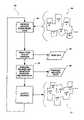
- an inventive method 30 for tracking integrated circuit (IC) devices through a step 32 in an IC manufacturing processincludes a step 34 of receiving IC devices from multiple, mixed lots 36 .
- IC devicesincluding Dynamic Random Access Memories (DRAMs), Static Random Access Memories (SRAMs), Synchronous DRAMs (SDRAMs), processors, Application Specific ICs (ASICs), Read Only Memory (ROM) ICs, Electrically Erasable Programmable ROM (EEPROM) ICs, and to mixtures of different types of IC devices.
- the step 32may be any step in an IC manufacturing process, including assembly and test steps.
- the step 32may encompass processing by a single machine, part of a machine, many machines operating in series or parallel, or any combination thereof.
- the step 34 of receiving IC devices from multiple, mixed lots 36is without regard to the lots from which the IC devices come, and thus allows a more efficient use of processing equipment than traditional lot-based procedures.
- the present inventionis described as being implemented in a single process step 32 for ease of understanding, the invention more typically is implemented on a series of process steps, such as all back-end test steps.
- the IC devicesare each programmed with a unique identification (ID) code, such as the well-known fuse ID described above.
- IDis programmed in an IC device by selectively blowing fuses or anti-fuses in a circuit on the IC device so that when the circuit is accessed, it outputs an ID code.
- ID code programmed into each IC devicebe unique by specifying, for example, a lot number, wafer number, and wafer position for the IC device, it is not necessary to implement the present invention. For example, if the ID code is the same for all IC devices derived from the same semiconductor wafer, or from the same lot, it will work for purposes of the present invention.
- data 40 related to the process step 32is generated for each IC device.
- data 40may include, for example, process variables such as the processing equipment used, the operating personnel present, the set-up, and the time and date of processing for the process step 32 , and performance variables such as yield and test results from the process step 32 .
- the set-up for the process step 32may include, for example, a standard set-up or a set-up in accordance with a Special Work Request (SWR) by engineering personnel.
- SWRSpecial Work Request
- the ID code data 38 and process-related data 40may be automatically correlated by computer with data from process steps prior to the process step 32 through reference to the ID codes common to the ID code data 38 generated in the process step 32 and ID code data generated in the prior process steps.
- correlationscan be found between process variables, such as the processing equipment used, and performance variables, such as test results.
- process variablessuch as the processing equipment used
- performance variablessuch as test results.
- the process of correlationis preferably performed in real time so information is available immediately, although it is within the scope of the present invention to perform the correlation at a later time.
- the processed IC devicesare output from the process step 32 to mixed output lots 42 . It should be understood that, in some cases, the processed IC devices must be cleared from processing equipment before other IC devices can be processed, and in other cases, such as in serial-feed machines, processed IC devices are being output from the process step 32 while other IC devices are advancing through the process step 32 and still other IC devices are being received by the process step 32 . Any of these cases fall within the scope of the present invention.
- the inventive method 30avoids the need for lot-based manufacturing altogether.
- the mixed input lots 36 and output lots 42may then be mixed without regard to lots, and the processing of IC devices through the process step 32 may proceed in a substantially continuous fashion, thus dramatically improving the utilization of processing equipment.
- the inventive methodis more reliable than conventional tracking procedures.
Landscapes
- Engineering & Computer Science (AREA)
- Physics & Mathematics (AREA)
- General Physics & Mathematics (AREA)
- General Engineering & Computer Science (AREA)
- Theoretical Computer Science (AREA)
- Quality & Reliability (AREA)
- Automation & Control Theory (AREA)
- Testing Or Measuring Of Semiconductors Or The Like (AREA)
- Semiconductor Integrated Circuits (AREA)
Abstract
Description
This application is a continuation of application Ser. No. 10/205,918, filed Jul. 25, 2002, now U.S. Pat. No. 7,555,358, issued Jun. 30, 2009, which is a continuation of application Ser. No. 09/137,781, filed Aug. 20, 1998, now U.S. Pat. No. 6,427,092, issued Jul. 30, 2002, which is a continuation of application Ser. No. 08/822,731, filed Mar. 24, 1997, now U.S. Pat. No. 5,856,923, issued Jan. 5, 1999, which is related to the following applications: Ser. No. 08/591,238, filed Jan. 17, 1996, now abandoned; Ser. No. 08/664,109, filed Jun. 13, 1996, now U.S. Pat. No. 5,895,962, issued Apr. 20, 1999; Ser. No. 08/785,353, filed Jan. 17, 1997, now U.S. Pat. No. 5,927,512, issued Jul. 27, 1999; Ser. No. 08/801,565, filed Feb. 17, 1997, now U.S. Pat. No. 5,844,803 issued Dec. 1, 1998; Ser. No. 08/806,442, filed Feb. 26, 1997, now U.S. Pat. No. 5,915,231, issued Jun. 22, 1999; and Ser. No. 08/871,015, filed Jun. 6, 1997, now U.S. Pat. No. 5,907,492, issued May 25, 1999. The disclosure of each of the previously referenced U.S. patent applications and patents is hereby incorporated by reference in its entirety.
1. Field of the Invention
The present invention relates in general to integrated circuit (IC) manufacturing and, more specifically, to methods for tracking IC devices in a substantially continuous flow of IC devices from multiple lots through one or more steps in an IC manufacturing process.
2. State of the Art
Integrated circuits (ICs) are small electronic circuits formed on the surface of a wafer of semiconductor material, such as silicon, in an IC manufacturing process referred to as “fabrication.” Once fabricated, ICs are probed to evaluate a variety of their electronic characteristics, cut from the wafer on which they were formed into discrete IC dice or “chips,” and then assembled for customer use using various well-known IC packaging techniques, including lead frame packaging, Chip-On-Board (COB) packaging, and flip-chip packaging.
During the manufacturing process, ICs generally undergo a variety of tests to ensure they will function properly once shipped. Testing typically involves a variety of known test steps, such as speed grading, burn-in, and final, which test ICs for defects and functionality and grade ICs for speed.
ICs are typically tracked through the fabrication, probe, assembly, and test steps described above so correlations can be found between the results of tests performed on ICs in the test steps and the“path” the ICs took through the manufacturing process. For example, by tracking a group of ICs through the manufacturing process, it might be determined that ICs wire-bonded on a particular wire-bonding machine have an unusually high failure rate when tested. Similarly, it might be determined that a test machine itself is failing a disproportionate number of ICs. In either case, tracking ICs through the manufacturing process allows the source of a problem to be pinpointed and addressed.
As shown inFIG. 1 , aconventional procedure 10 for tracking ICs through aprocess step 12 in an IC manufacturing process involves the use of lot numbers for the ICs. Lot numbers are first assigned to wafers during fabrication. Typically, a group of 20-50 wafers receives a single unique lot number (e.g., 36/1/9970). As the group of wafers proceeds to probe, the wafers are typically split into several sub-lots, with each sub-lot being assigned a new lot number (sometimes referred to as a “sub-lot” number) that is a modified form of the group's original lot number (e.g., 36/1/9970/0, 36/1/9970/1, . . . ). As the group continues through the manufacturing process, sub-lots are split and re-split for a variety of reasons until the group is typically split into many sub-lots, all having a unique lot number that is a modified form of the group's original lot number.
In theconventional tracking procedure 10, a sub-lot (e.g., sub-lot H) is received from aninput queue 14 where sub-lots wait to proceed through theprocess step 12. Theprocess step 12 may be any step in the IC manufacturing process including, for example, probe, wafer saw, speed grading, burn-in, or final testing.
As a sub-lot advances through theprocess step 12,data 16 related to theprocess step 12 is generated.Such data 16 may include, for example: an identification of the processing equipment and the operating personnel for theprocess step 12; information regarding the set-up of theprocess step 12; the time and date the sub-lot advanced through theprocess step 12; and yield and test results from theprocess step 12.
Once a sub-lot has advanced through theprocess step 12, aprocess report 18 is manually or automatically generated based on the generateddata 16. To associate thereport 18, and hence thedata 16, with the ICs in the sub-lot, and thus track the ICs through theprocess step 12, thereport 18 lists the lot number (e.g., “H”) of the ICs in the sub-lot. Typically, thereport 18 also physically accompanies the sub-lot through the remainder of the manufacturing process to insure that thedata 16 is correlated with the ICs in the sub-lot, although this is not necessary if other indicia identifying the lot number of the ICs in the sub-lot physically accompany the sub-lot through the manufacturing process.
With thereport 18 generated, a processed sub-lot (e.g., sub-lot H) is cleared from equipment associated with theprocess step 12 to anoutput queue 20 to prepare theprocess step 12 for processing another sub-lot (e.g., sub-lot I). Once the processed sub-lot is cleared, the next sub-lot can be processed. This “clearing” process is necessary because if two sub-lots (e.g., sub-lots H and I) proceed through theprocess step 12 in a continuous manner, theconventional tracking procedure 10 is unable to correlate thedata 16 and theprocess report 18 generated as each of the two sub-lots proceed with the correct sub-lot. Instead, thedata 16 for the two sub-lots is mixed, causing theconventional tracking procedure 10 to fail to uniquely track the two sub-lots through theprocess step 12.
The conventional tracking procedure described above is problematic because it makes inefficient use of often very expensive manufacturing and test equipment and other resources by leaving sub-lots “parked” in input queues while process reports are generated and the equipment is cleared of already processed sub-lots. In process steps that use multiple machines in parallel to process a sub-lot, some machines may be idle while other machines finish their allotment from the sub-lot being processed and the next sub-lot waits in an input queue. In addition, generation of the process reports, as well as clearing a processed sub-lot from equipment, often requires laborious manual work by operating personnel. Further, a process report that must physically accompany a sub-lot through the manufacturing process may become lost or damaged. And thus is not as reliable a means of tracking ICs as is desired.
As described in U.S. Pat. Nos. 5,301,143, 5,294,812, and 5,103,166, some methods have been devised to aid quality control personnel in tracking ICs undergoing failure analysis back to the wafer from which they come. By tracking the ICs back to their wafer, test data related to the ICs can be correlated to the wafer to pinpoint possible problems with the wafer. Such methods take place “off” the manufacturing line, and involve the use of electrically retrievable identification (ID) codes, such as so-called “fuse IDs,” programmed into individual ICs to identify the ICs. Fuse IDs and other electrically retrievable ID codes are typically programmed into ICs by blowing selected fuses or anti-fuses in circuitry on the ICs so that the circuitry outputs the ID code when accessed. Unfortunately, none of these methods addresses the inefficiency problems caused by the conventional lot-based tracking procedure described above.
Therefore, there is a need in the art for a procedure for tracking ICs through an IC manufacturing process that uses manufacturing resources more efficiently. Such a procedure should not leave equipment idle while ICs wait to be processed. In addition, such a procedure should achieve a level of reliability not reached by conventional tracking procedures.
An inventive method for tracking integrated circuit (IC) devices of the type to each have a substantially unique identification (ID) code (e.g., a fuse ID) through a step in an IC manufacturing process includes: reading the ID code of each of the IC devices; advancing multiple lots of the IC devices through the step in the manufacturing process in a substantially continuous manner; generating data, such as processing equipment data or test data, related to the advancement of each of the IC devices trough the step in the process; and associating the data generated for each of the IC devices with the ID code of its associated IC device.
- By associating the data with the ID codes, the inventive method allows the IC devices to be tracked through the step in the process. Further, because multiple lots of the IC devices can advance through the step in the manufacturing process continuously, manufacturing resources are used more efficiently. In addition, because the ID codes and associated data read and generated using the inventive method need not physically accompany ICs as they progress through the manufacturing process, the inventive method is more reliable than conventional tracking procedures.
In another embodiment, a method of manufacturing IC devices from semiconductor wafers includes: providing wafers in multiple lots; fabricating ICs on the wafers; causing each of the ICs to permanently store a substantially unique ID code, such as a fuse ID; separating the ICs from their wafers to form IC dice; assembling the IC dice into IC devices; reading the IC code from the IC in each of the IC devices; testing each of the IC devices; while testing the IC devices: advancing the IC devices from the multiple lots of wafers through at least one test step in a substantially continuous manner; generating data related to the advancement of each of the IC devices through the test step; and associating the data generated for each of the IC devices with the ID code of the IC in its associated IC device.
In a further embodiment, a method for correlating variables related to an IC manufacturing process with variables related to the performance of IC devices as they advance through the process includes: causing each of multiple ICs from multiple lots to permanently store a substantially unique ID code, such as a fuse ID; reading the ID code from each of the IC devices; advancing the IC devices from the multiple lots through at least one step in the manufacturing process in a substantially continuous manner; while the IC devices advance through the step in the manufacturing process, generating data related to process variables associated with the step in the process; generating data related to variables associated with the performance of at least some of the IC devices as they advance through at least one step in the manufacturing process; and associating the process variable-related data and the performance variable-related data generated for each of the IC devices with the ID code of the IC device associated with the data to correlate the process variables with the performance variables.
As shown inFIG. 2 , aninventive method 30 for tracking integrated circuit (IC) devices through astep 32 in an IC manufacturing process includes astep 34 of receiving IC devices from multiple,mixed lots 36. It will be understood by those having skill in the field of this invention that the invention is applicable to any IC devices, including Dynamic Random Access Memories (DRAMs), Static Random Access Memories (SRAMs), Synchronous DRAMs (SDRAMs), processors, Application Specific ICs (ASICs), Read Only Memory (ROM) ICs, Electrically Erasable Programmable ROM (EEPROM) ICs, and to mixtures of different types of IC devices. Further, it will be understood that thestep 32 may be any step in an IC manufacturing process, including assembly and test steps. It will also be understood that thestep 32 may encompass processing by a single machine, part of a machine, many machines operating in series or parallel, or any combination thereof. In addition, it will be understood that thestep 34 of receiving IC devices from multiple,mixed lots 36 is without regard to the lots from which the IC devices come, and thus allows a more efficient use of processing equipment than traditional lot-based procedures. It will also be understood, of course, that although the present invention is described as being implemented in asingle process step 32 for ease of understanding, the invention more typically is implemented on a series of process steps, such as all back-end test steps.
The IC devices are each programmed with a unique identification (ID) code, such as the well-known fuse ID described above. Briefly, a fuse ID is programmed in an IC device by selectively blowing fuses or anti-fuses in a circuit on the IC device so that when the circuit is accessed, it outputs an ID code. Although it is preferable that the ID code programmed into each IC device be unique by specifying, for example, a lot number, wafer number, and wafer position for the IC device, it is not necessary to implement the present invention. For example, if the ID code is the same for all IC devices derived from the same semiconductor wafer, or from the same lot, it will work for purposes of the present invention.
Before or after the IC devices progress through theprocess step 32, their ID codes are read and stored in a computer asdata 38. As the IC devices progress through theprocess step 32,data 40 related to theprocess step 32 is generated for each IC device.Such data 40 may include, for example, process variables such as the processing equipment used, the operating personnel present, the set-up, and the time and date of processing for theprocess step 32, and performance variables such as yield and test results from theprocess step 32. The set-up for theprocess step 32 may include, for example, a standard set-up or a set-up in accordance with a Special Work Request (SWR) by engineering personnel.
TheID code data 38 and process-relateddata 40 may be automatically correlated by computer with data from process steps prior to theprocess step 32 through reference to the ID codes common to theID code data 38 generated in theprocess step 32 and ID code data generated in the prior process steps. As a result, correlations can be found between process variables, such as the processing equipment used, and performance variables, such as test results. Thus for example, it might be discerned that the IC devices derived from a particular section of the semiconductor wafers provided by a particular supplier have an unusually high failure rate at a particular test step. The process of correlation is preferably performed in real time so information is available immediately, although it is within the scope of the present invention to perform the correlation at a later time.
Once the IC devices have advanced through theprocess step 32, the processed IC devices are output from theprocess step 32 tomixed output lots 42. It should be understood that, in some cases, the processed IC devices must be cleared from processing equipment before other IC devices can be processed, and in other cases, such as in serial-feed machines, processed IC devices are being output from theprocess step 32 while other IC devices are advancing through theprocess step 32 and still other IC devices are being received by theprocess step 32. Any of these cases fall within the scope of the present invention.
It should be understood that by reading the ID codes of processed IC devices and associating those codes with data generated during processing, theinventive method 30 avoids the need for lot-based manufacturing altogether. Themixed input lots 36 andoutput lots 42 may then be mixed without regard to lots, and the processing of IC devices through theprocess step 32 may proceed in a substantially continuous fashion, thus dramatically improving the utilization of processing equipment. In additions because the ID codes and associated data read and generated using the inventive method need not physically accompany ICs as they progress through the manufacturing process, the inventive method is more reliable than conventional tracking procedures.
Although the present invention has been described with reference to a particular embodiment, the invention is not limited to this described embodiment. For example, the present invention includes within its scope the manufacture of Single In-line Memory Modules (SIMMs) and Dual In-line Memory Modules (DIMMs), as well as the IC devices described above. Thus, the invention is limited only by the appended claims, which include within their scope all equivalent that operate according to the principles of the invention as described.
Claims (20)
1. A method for tracking at least one integrated circuit device comprising:
providing each integrated circuit device of a plurality of integrated circuit devices with at least one identification code in a lot of integrated circuit devices of a plurality of lots of integrated circuit devices;
reading the at least one identification code of each integrated circuit device of the plurality of integrated circuit devices in a lot of integrated circuit devices of a plurality of lots of integrated circuit devices;
advancing the plurality of integrated circuit devices through a manufacturing process in a substantially continuous manner after mixing at least one integrated circuit device of the integrated circuit devices from one lot to another lot of the plurality of lots of integrated circuit devices without regard to the lot of the plurality of lots from which the integrated circuit devices come during the manufacturing process;
generating data related to the advancement of each integrated circuit device of the plurality of integrated circuit devices through at least a portion of the manufacturing process; and
associating the data generated for each integrated circuit device of the plurality of integrated circuit devices with the at least one identification code for an associated integrated circuit device of the plurality of integrated circuit devices.
2. A method for tracking at least one integrated circuit device of a plurality of integrated circuit devices in a manufacturing process comprising:
forming a unique identification code using a fuse in each integrated circuit device of the plurality of integrated circuit devices for reading the identification code of each integrated circuit device of the plurality of integrated circuit devices in a lot of integrated circuit devices of a plurality of lots of integrated circuit devices;
advancing the plurality of integrated circuit devices in each lot of a plurality of lots of integrated circuit devices after the integrated circuit devices of the plurality of lots of integrated circuit devices have been mixed from one lot to another lot without regard to the lot of the plurality of lots from which the integrated circuit devices come during the manufacturing process;
generating data related to the advancement of each integrated circuit device of the plurality of integrated circuit devices in each lot of a plurality of lots of integrated circuit devices through a portion of the manufacturing process; and
associating the data generated for each integrated circuit device of the plurality of integrated circuit devices with the identification code in each lot of a plurality of lots of integrated circuit devices.
3. The method ofclaim 2 , wherein each integrated circuit device of the plurality of integrated circuit devices is programmed with at least one substantially unique, electrically retrievable identification code for the reading of the at least one identification code of each integrated circuit device of the plurality of integrated circuit devices comprising electrically retrieving the at least one substantially unique, electrically retrievable identification code of each integrated circuit device of the plurality of integrated circuit devices.
4. The method ofclaim 2 , wherein each integrated circuit device of the plurality of integrated circuit devices is programmed with at least one unique fuse identification code for the reading of the at least one identification code of each integrated circuit device of the plurality of integrated circuit devices comprising reading the at least one unique fuse identification code programmed into each integrated circuit device of the plurality of integrated circuit devices.
5. The method ofclaim 2 , wherein advancing the plurality of integrated circuit devices through the manufacturing process includes advancing the plurality of integrated circuit devices through an assembly step.
6. The method ofclaim 2 , wherein advancing the plurality of integrated circuit devices through the manufacturing process includes advancing the plurality of integrated circuit devices through a test procedure.
7. The method ofclaim 2 , further comprising reading the at least one identification code of each integrated circuit device of the plurality of integrated circuit devices occurs before advancing the plurality of integrated circuit devices through the manufacturing process.
8. The method ofclaim 2 , wherein advancing the plurality of integrated circuit devices through the manufacturing process includes serially advancing each integrated circuit device of the plurality of integrated circuit devices through multiple machines associated with the manufacturing process.
9. The method ofclaim 2 , wherein advancing the plurality of integrated circuit devices through the manufacturing process includes advancing the plurality of integrated circuit devices through parallel machines associated with the manufacturing process.
10. The method ofclaim 2 , wherein generating data related to the advancement of each integrated circuit device of the plurality of integrated circuit devices through the at least a portion of the manufacturing process comprises generating data selected from a group consisting of processing equipment data, processing personnel data, processing set-up data, time and date data, yield data, and test data.
11. The method ofclaim 2 , further comprising storing the at least one identification code of each integrated circuit device of the plurality of integrated circuit devices, the associating of data generated for each integrated circuit device of the plurality of integrated circuit devices with the at least one identification code of its associated integrated circuit device comprising storing the data generated for each integrated circuit device of the plurality of integrated circuit devices in association with the stored at least one identification code of its associated integrated circuit device.
12. The method ofclaim 2 , wherein each integrated circuit device of the plurality of integrated circuit devices has an associated lot identification code and the associating data generated for each integrated circuit device of the plurality of integrated circuit devices with the at least one identification code of its associated integrated circuit device comprising storing the data generated for each integrated circuit device of the plurality of integrated circuit devices in association with the lot identification code of its associated integrated circuit device.
13. A method for tracking a manufacturing process using at least one integrated circuit device of a plurality of integrated circuit devices in the manufacturing process comprising:
forming a unique identification code using a fuse in each integrated circuit device of the plurality of integrated circuit devices in a lot of integrated circuit devices of a plurality of lots of integrated circuit devices for reading the identification code of each integrated circuit device of the plurality of integrated circuit devices;
mixing the integrated circuit devices from the plurality of lots of integrated circuit devices from one lot to another without regard to the lot of the plurality of lots from which the integrated circuit devices come during the manufacturing process;
advancing the plurality of integrated circuit devices through a first portion of the manufacturing process;
forming a unique identification code using a fuse in each integrated circuit device of the plurality of integrated circuit devices for reading the identification code of each integrated circuit device of the plurality of integrated circuit devices associated with the first portion of the manufacturing process;
advancing the plurality of integrated circuit devices through a second portion of the manufacturing process;
forming a unique identification code using a fuse in each integrated circuit device of the plurality of integrated circuit devices for reading the identification code of each integrated circuit device of the plurality of integrated circuit devices associated with the second portion of the manufacturing process;
generating data related to the advancement of each integrated circuit device of the plurality of integrated circuit devices through the first portion and the second portion of the manufacturing process; and
associating the data generated for each integrated circuit device of the plurality of integrated circuit devices with the identification code for the first portion and the second portion of the manufacturing process.
14. The method ofclaim 13 , wherein each integrated circuit device of the plurality of integrated circuit devices is programmed with at least one substantially unique, electrically retrievable identification code for the reading of the at least one identification code of each integrated circuit device of the plurality of integrated circuit devices comprising electrically retrieving the at least one substantially unique, electrically retrievable identification code of each integrated circuit device of the plurality of integrated circuit devices for advancing the plurality of integrated circuit devices through an assembly step.
15. The method ofclaim 13 , wherein each integrated circuit device of the plurality of integrated circuit devices is programmed with at least one unique fuse identification code, the reading of the at least one identification code of each integrated circuit device of the plurality of integrated circuit devices comprising reading the at least one unique fuse identification code programmed into each integrated circuit device of the plurality of integrated circuit devices for advancing the plurality of integrated circuit devices through a test procedure.
16. The method ofclaim 13 , wherein advancing the plurality of integrated circuit devices through the manufacturing process includes advancing the plurality of integrated circuit devices through one of an assembly step and a test procedure.
17. The method ofclaim 13 , further comprising reading the at least one identification code of each integrated circuit device of the plurality of integrated circuit devices occurs before advancing the plurality of integrated circuit devices through the manufacturing process wherein advancing the plurality of integrated circuit devices through the manufacturing process includes serially advancing each integrated circuit device of the plurality of integrated circuit devices through multiple machines associated with the manufacturing process.
18. The method ofclaim 13 , wherein advancing the plurality of integrated circuit devices through the manufacturing process includes advancing the plurality of integrated circuit devices through parallel machines associated with the manufacturing process.
19. The method ofclaim 13 , further comprising storing the at least one identification code of each integrated circuit device of the plurality of integrated circuit devices for the associating the data generated for each integrated circuit device of the plurality of integrated circuit devices with the at least one identification code of its associated integrated circuit device comprising storing the data generated for each integrated circuit device of the plurality of integrated circuit devices in association with the stored at least one identification code of its associated integrated circuit device.
20. The method ofclaim 13 , wherein each integrated circuit device of the plurality of integrated circuit devices has an associated lot identification code and the associating data generated for each integrated circuit device of the plurality of integrated circuit devices with the at least one identification code of its associated integrated circuit device comprising storing the data generated for each integrated circuit device of the plurality of integrated circuit devices in association with the lot identification code of its associated integrated circuit device.
Priority Applications (3)
| Application Number | Priority Date | Filing Date | Title |
|---|---|---|---|
| US11/763,104US7738988B2 (en) | 1997-03-24 | 2007-06-14 | Process and method for continuous, non lot-based integrated circuit manufacturing |
| US12/776,625US8315730B2 (en) | 1997-03-24 | 2010-05-10 | Methods for non lot-based integrated circuit manufacturing |
| US13/615,018US8600540B2 (en) | 1997-03-24 | 2012-09-13 | Methods for non-lot-based manufacturing of articles |
Applications Claiming Priority (4)
| Application Number | Priority Date | Filing Date | Title |
|---|---|---|---|
| US08/822,731US5856923A (en) | 1997-03-24 | 1997-03-24 | Method for continuous, non lot-based integrated circuit manufacturing |
| US09/137,781US6427092B1 (en) | 1997-03-24 | 1998-08-20 | Method for continuous, non lot-based integrated circuit manufacturing |
| US10/205,918US7555358B2 (en) | 1997-03-24 | 2002-07-25 | Process and method for continuous, non lot-based integrated circuit manufacturing |
| US11/763,104US7738988B2 (en) | 1997-03-24 | 2007-06-14 | Process and method for continuous, non lot-based integrated circuit manufacturing |
Related Parent Applications (1)
| Application Number | Title | Priority Date | Filing Date |
|---|---|---|---|
| US10/205,918ContinuationUS7555358B2 (en) | 1997-03-24 | 2002-07-25 | Process and method for continuous, non lot-based integrated circuit manufacturing |
Related Child Applications (1)
| Application Number | Title | Priority Date | Filing Date |
|---|---|---|---|
| US12/776,625ContinuationUS8315730B2 (en) | 1997-03-24 | 2010-05-10 | Methods for non lot-based integrated circuit manufacturing |
Publications (2)
| Publication Number | Publication Date |
|---|---|
| US20070239307A1 US20070239307A1 (en) | 2007-10-11 |
| US7738988B2true US7738988B2 (en) | 2010-06-15 |
Family
ID=25236814
Family Applications (6)
| Application Number | Title | Priority Date | Filing Date |
|---|---|---|---|
| US08/822,731Expired - LifetimeUS5856923A (en) | 1997-03-24 | 1997-03-24 | Method for continuous, non lot-based integrated circuit manufacturing |
| US09/137,781Expired - LifetimeUS6427092B1 (en) | 1997-03-24 | 1998-08-20 | Method for continuous, non lot-based integrated circuit manufacturing |
| US10/205,918Expired - Fee RelatedUS7555358B2 (en) | 1997-03-24 | 2002-07-25 | Process and method for continuous, non lot-based integrated circuit manufacturing |
| US11/763,104Expired - Fee RelatedUS7738988B2 (en) | 1997-03-24 | 2007-06-14 | Process and method for continuous, non lot-based integrated circuit manufacturing |
| US12/776,625Expired - Fee RelatedUS8315730B2 (en) | 1997-03-24 | 2010-05-10 | Methods for non lot-based integrated circuit manufacturing |
| US13/615,018Expired - Fee RelatedUS8600540B2 (en) | 1997-03-24 | 2012-09-13 | Methods for non-lot-based manufacturing of articles |
Family Applications Before (3)
| Application Number | Title | Priority Date | Filing Date |
|---|---|---|---|
| US08/822,731Expired - LifetimeUS5856923A (en) | 1997-03-24 | 1997-03-24 | Method for continuous, non lot-based integrated circuit manufacturing |
| US09/137,781Expired - LifetimeUS6427092B1 (en) | 1997-03-24 | 1998-08-20 | Method for continuous, non lot-based integrated circuit manufacturing |
| US10/205,918Expired - Fee RelatedUS7555358B2 (en) | 1997-03-24 | 2002-07-25 | Process and method for continuous, non lot-based integrated circuit manufacturing |
Family Applications After (2)
| Application Number | Title | Priority Date | Filing Date |
|---|---|---|---|
| US12/776,625Expired - Fee RelatedUS8315730B2 (en) | 1997-03-24 | 2010-05-10 | Methods for non lot-based integrated circuit manufacturing |
| US13/615,018Expired - Fee RelatedUS8600540B2 (en) | 1997-03-24 | 2012-09-13 | Methods for non-lot-based manufacturing of articles |
Country Status (5)
| Country | Link |
|---|---|
| US (6) | US5856923A (en) |
| EP (1) | EP1027675A4 (en) |
| JP (1) | JP3360733B2 (en) |
| KR (1) | KR100430174B1 (en) |
| WO (1) | WO1998043191A1 (en) |
Cited By (2)
| Publication number | Priority date | Publication date | Assignee | Title |
|---|---|---|---|---|
| US8600540B2 (en) | 1997-03-24 | 2013-12-03 | Micron Technology, Inc. | Methods for non-lot-based manufacturing of articles |
| US20180002826A1 (en)* | 2016-06-30 | 2018-01-04 | Infineon Technologies Ag | Method of manufacturing cz silicon wafers, and method of manufacturing a semiconductor device |
Families Citing this family (60)
| Publication number | Priority date | Publication date | Assignee | Title |
|---|---|---|---|---|
| WO2000057458A1 (en)* | 1999-03-24 | 2000-09-28 | Fujitsu Limited | Method of manufacturing semiconductor device and semiconductor device manufactured by it |
| US5927512A (en)* | 1997-01-17 | 1999-07-27 | Micron Technology, Inc. | Method for sorting integrated circuit devices |
| US6100486A (en) | 1998-08-13 | 2000-08-08 | Micron Technology, Inc. | Method for sorting integrated circuit devices |
| US5844803A (en) | 1997-02-17 | 1998-12-01 | Micron Technology, Inc. | Method of sorting a group of integrated circuit devices for those devices requiring special testing |
| US5915231A (en) | 1997-02-26 | 1999-06-22 | Micron Technology, Inc. | Method in an integrated circuit (IC) manufacturing process for identifying and redirecting IC's mis-processed during their manufacture |
| US7120513B1 (en)* | 1997-06-06 | 2006-10-10 | Micron Technology, Inc. | Method for using data regarding manufacturing procedures integrated circuits (ICS) have undergone, such as repairs, to select procedures the ICS will undergo, such as additional repairs |
| US5907492A (en)* | 1997-06-06 | 1999-05-25 | Micron Technology, Inc. | Method for using data regarding manufacturing procedures integrated circuits (IC's) have undergone, such as repairs, to select procedures the IC's will undergo, such as additional repairs |
| US6446017B1 (en)* | 1997-08-21 | 2002-09-03 | Micron Technology, Inc. | Method and system for tracking manufacturing data for integrated circuit parts |
| US6092000A (en)* | 1997-10-28 | 2000-07-18 | Vanguard International Semiconductor Corporation | Method for maximizing the throughput of a multiple-step workstation in a plant |
| US6049624A (en)* | 1998-02-20 | 2000-04-11 | Micron Technology, Inc. | Non-lot based method for assembling integrated circuit devices |
| US6238942B1 (en)* | 1998-04-07 | 2001-05-29 | Micron Technology, Inc. | Method of wire-bonding a repair die in a multi-chip module using a repair solution generated during testing of the module |
| US6314547B1 (en)* | 1998-09-11 | 2001-11-06 | International Business Machines Corporation | Method for improving the assignment of circuit locations during fabrication |
| US6360133B1 (en)* | 1999-06-17 | 2002-03-19 | Advanced Micro Devices, Inc. | Method and apparatus for automatic routing for reentrant process |
| US6990387B1 (en)* | 2000-05-18 | 2006-01-24 | Intel Corporation | Test system for identification and sorting of integrated circuit devices |
| US6524881B1 (en)* | 2000-08-25 | 2003-02-25 | Micron Technology, Inc. | Method and apparatus for marking a bare semiconductor die |
| US20020147946A1 (en)* | 2001-04-05 | 2002-10-10 | Yong Jaimsomporn | Method and system for automatic test report generation from memory device reliabilty testing |
| MY127433A (en)* | 2001-05-29 | 2006-12-29 | Integrated Device Tech | Die bonding apparatus with automatic die and lead frame image matching system. |
| WO2003003138A2 (en)* | 2001-06-27 | 2003-01-09 | Nokia Corporation | Method and system for efficient management and transport of traffic over a network |
| US6961880B2 (en)* | 2001-07-30 | 2005-11-01 | Infineon Technologies Ag | Recording test information to identify memory cell errors |
| US6792365B2 (en)* | 2001-08-10 | 2004-09-14 | Micron Technology, Inc. | Sequential unique marking |
| US7169685B2 (en)* | 2002-02-25 | 2007-01-30 | Micron Technology, Inc. | Wafer back side coating to balance stress from passivation layer on front of wafer and be used as die attach adhesive |
| US7046536B2 (en)* | 2002-05-29 | 2006-05-16 | Micron Technology, Inc. | Programable identification circuitry |
| US8321048B1 (en)* | 2002-06-28 | 2012-11-27 | Advanced Micro Devices, Inc. | Associating data with workpieces and correlating the data with yield data |
| US6952623B2 (en)* | 2002-07-02 | 2005-10-04 | Texas Instruments, Inc. | Permanent chip ID using FeRAM |
| US7668702B2 (en)* | 2002-07-19 | 2010-02-23 | Applied Materials, Inc. | Method, system and medium for controlling manufacturing process using adaptive models based on empirical data |
| JP3736525B2 (en)* | 2002-12-25 | 2006-01-18 | ソニー株式会社 | Semiconductor integrated circuit device and circuit board |
| JP4449319B2 (en)* | 2003-03-25 | 2010-04-14 | 株式会社デンソー | Manufacturing management method |
| US7017429B2 (en)* | 2003-04-30 | 2006-03-28 | Infineon Technologies Richmond, Lp | Continuous test flow method and apparatus |
| US6954711B2 (en)* | 2003-05-19 | 2005-10-11 | Applied Materials, Inc. | Test substrate reclamation method and apparatus |
| JP4215677B2 (en)* | 2003-08-25 | 2009-01-28 | 日立ビアメカニクス株式会社 | Laser processing machine and laser processing method |
| US20050152594A1 (en)* | 2003-11-10 | 2005-07-14 | Hermes-Microvision, Inc. | Method and system for monitoring IC process |
| US7415317B2 (en)* | 2004-02-25 | 2008-08-19 | Micron Technology, Inc. | Method and system for correlating and combining production and non-production data for analysis |
| US7395130B2 (en)* | 2004-02-27 | 2008-07-01 | Micron Technology, Inc. | Method and system for aggregating and combining manufacturing data for analysis |
| US7512455B2 (en)* | 2004-03-29 | 2009-03-31 | Palo Alto Research Center Incorporated | Method for self-synchronization of modular production systems |
| US7185888B2 (en) | 2004-03-29 | 2007-03-06 | Palo Alto Research Center Incorporated | Rotational jam clearance apparatus |
| EP1810326A1 (en)* | 2004-10-15 | 2007-07-25 | Applied Materials, Inc. | Die-level traceability mechanism for semiconductor assembly and test facility |
| US7657390B2 (en)* | 2005-11-02 | 2010-02-02 | Applied Materials, Inc. | Reclaiming substrates having defects and contaminants |
| US7487003B1 (en)* | 2006-03-09 | 2009-02-03 | Rockwell Automation Technologies, Inc. | Automatic tracking of a lot of items through virtual sublots |
| DE102006039207B3 (en)* | 2006-08-22 | 2008-04-03 | Hans-Georg Zwicker | System and method for organizing workpieces to be machined |
| US20080294282A1 (en)* | 2007-05-24 | 2008-11-27 | Applied Materials, Inc. | Use of logical lots in semiconductor substrate processing |
| EP2051189A1 (en)* | 2007-10-18 | 2009-04-22 | Siemens Aktiengesellschaft | Device for electronic identification of items |
| DE102007062376A1 (en)* | 2007-12-22 | 2009-06-25 | Dietz-Automotive Gmbh & Co. Kg | Method for assembling an assembly |
| US7908023B2 (en)* | 2008-01-14 | 2011-03-15 | International Business Machines Corporation | Method of establishing a lot grade system for product lots in a semiconductor manufacturing process |
| JP5433290B2 (en)* | 2009-04-20 | 2014-03-05 | 東京エレクトロン株式会社 | Substrate storage method and control device |
| EP4092590B1 (en)* | 2009-07-10 | 2025-07-02 | Malikie Innovations Limited | System and method for performing serialization of devices |
| US8689434B2 (en)* | 2009-10-14 | 2014-04-08 | Nanya Technology Corporation | Integrated circuit manufacturing system |
| JP2011098808A (en)* | 2009-11-05 | 2011-05-19 | Nikon Corp | Substrate cartridge, substrate processing device, substrate processing system, substrate processing method, control device and method of manufacturing display element |
| TWI442401B (en)* | 2009-12-30 | 2014-06-21 | Macronix Int Co Ltd | 3d chip select for sheard input packages |
| JP5968705B2 (en)* | 2012-07-13 | 2016-08-10 | ルネサスエレクトロニクス株式会社 | Manufacturing method of semiconductor device |
| GB2505489A (en) | 2012-08-31 | 2014-03-05 | Sony Corp | A mobile communications device for use in a virtual narrowband carrier within a wideband carrier of a mobile communications system |
| KR102021819B1 (en)* | 2012-12-14 | 2019-09-17 | 삼성전자주식회사 | System for testing a semiconductor module |
| US9678501B2 (en)* | 2013-01-08 | 2017-06-13 | Bloom Energy Corporation | Serialization of fuel cell components |
| US9305816B2 (en) | 2013-12-28 | 2016-04-05 | Intel Corporation | Methods and devices for securing and transporting singulated die in high volume manufacturing |
| US9823303B1 (en) | 2014-03-14 | 2017-11-21 | Altera Corporation | Methods for selecting integrated circuit dies based on pre-determined criteria |
| US9559113B2 (en) | 2014-05-01 | 2017-01-31 | Macronix International Co., Ltd. | SSL/GSL gate oxide in 3D vertical channel NAND |
| CN106537990B (en)* | 2014-07-11 | 2019-11-01 | 华为技术有限公司 | For the network equipment, user equipment and the method for access signal broadcast |
| EP3709746B1 (en)* | 2014-12-01 | 2024-09-04 | International Semiconductor Group | Wireless communication terminal and wireless communication method |
| KR102653937B1 (en)* | 2018-07-17 | 2024-04-02 | 삼성전자주식회사 | Test method for semiconductor devices and test system for semiconductor devices |
| GB2581861B (en)* | 2018-09-14 | 2022-10-05 | Sino Ic Tech Co Ltd | IC Test Information Management System Based on Industrial Internet |
| CN110349887A (en)* | 2019-07-16 | 2019-10-18 | 沛顿科技(深圳)有限公司 | The system of the single IC condition of production of retrospect based on two dimensional code |
Citations (127)
| Publication number | Priority date | Publication date | Assignee | Title |
|---|---|---|---|---|
| US4027246A (en) | 1976-03-26 | 1977-05-31 | International Business Machines Corporation | Automated integrated circuit manufacturing system |
| US4032949A (en) | 1975-05-15 | 1977-06-28 | Raytheon Company | Integrated circuit fusing technique |
| US4150331A (en) | 1977-07-29 | 1979-04-17 | Burroughs Corporation | Signature encoding for integrated circuits |
| JPS5850728A (en) | 1981-09-19 | 1983-03-25 | Mitsubishi Electric Corp | Manufacture of semiconductor device |
| JPS5852814A (en) | 1981-09-24 | 1983-03-29 | Nec Corp | Semiconductor integrated circuit |
| JPS5860529A (en) | 1981-10-06 | 1983-04-11 | Mitsubishi Electric Corp | Identifying method for semiconductor chip |
| US4454413A (en) | 1982-02-19 | 1984-06-12 | Precision Monolithics, Inc. | Apparatus for tracking integrated circuit devices |
| US4455495A (en) | 1979-10-01 | 1984-06-19 | Hitachi, Ltd. | Programmable semiconductor integrated circuitry including a programming semiconductor element |
| US4460999A (en) | 1981-07-15 | 1984-07-17 | Pacific Western Systems, Inc. | Memory tester having memory repair analysis under pattern generator control |
| US4510673A (en) | 1983-06-23 | 1985-04-16 | International Business Machines Corporation | Laser written chip identification method |
| US4534014A (en) | 1983-06-20 | 1985-08-06 | Ames Oliver C | Mechanically programmable read only memory |
| JPS61120433A (en) | 1984-11-16 | 1986-06-07 | Toshiba Corp | die bonding equipment |
| US4667403A (en) | 1984-05-16 | 1987-05-26 | Siemens Aktiengesellschaft | Method for manufacturing electronic card modules |
| US4736373A (en) | 1981-08-03 | 1988-04-05 | Pacific Western Systems, Inc. | Memory tester having concurrent failure data readout and memory repair analysis |
| US4796194A (en)* | 1986-08-20 | 1989-01-03 | Atherton Robert W | Real world modeling and control process |
| US4871963A (en) | 1986-07-22 | 1989-10-03 | Sgs Microelettronica S.P.A. | Method and apparatus for testing EPROM type semiconductor devices during burn-in |
| US4954453A (en) | 1989-02-24 | 1990-09-04 | At&T Bell Laboratories | Method of producing an article comprising a multichip assembly |
| US4958373A (en) | 1987-03-31 | 1990-09-18 | Kabushiki Kaisha Toshiba | Defect-recognition processing apparatus |
| US4967381A (en) | 1985-04-30 | 1990-10-30 | Prometrix Corporation | Process control interface system for managing measurement data |
| US4985988A (en) | 1989-11-03 | 1991-01-22 | Motorola, Inc. | Method for assembling, testing, and packaging integrated circuits |
| US5003251A (en) | 1989-09-12 | 1991-03-26 | Grumman Aerospace Corporation | Bar code reader for printed circuit board |
| US5014208A (en)* | 1989-01-23 | 1991-05-07 | Siemens Corporate Research, Inc. | Workcell controller employing entity-server model for physical objects and logical abstractions |
| US5043657A (en) | 1990-07-13 | 1991-08-27 | Analog Devices, Incorporated | Marking techniques for identifying integrated circuit parts at the time of testing |
| US5103166A (en) | 1990-05-23 | 1992-04-07 | Samsung Electronics Co., Ltd. | Semiconductor integrated circuit chip having an identification circuit therein |
| US5105362A (en) | 1987-04-03 | 1992-04-14 | Mitsubishi Denki Kabushiki Kaisha | Method for producing semiconductor devices |
| US5110754A (en) | 1991-10-04 | 1992-05-05 | Micron Technology, Inc. | Method of making a DRAM capacitor for use as an programmable antifuse for redundancy repair/options on a DRAM |
| US5118369A (en) | 1990-08-23 | 1992-06-02 | Colorcode Unlimited Corporation | Microlabelling system and process for making microlabels |
| US5150331A (en) | 1991-03-25 | 1992-09-22 | Amoco Corporation | Method for enhancing seismic data |
| US5175774A (en) | 1990-10-16 | 1992-12-29 | Micron Technology, Inc. | Semiconductor wafer marking for identification during processing |
| US5197650A (en) | 1990-09-18 | 1993-03-30 | Sharp Kabushiki Kaisha | Die bonding apparatus |
| US5217834A (en) | 1990-08-14 | 1993-06-08 | Kabushiki Kaisha Toshiba | Methods of forming and inspecting semiconductor device patterns |
| US5219765A (en) | 1990-09-12 | 1993-06-15 | Hitachi, Ltd. | Method for manufacturing a semiconductor device including wafer aging, probe inspection, and feeding back the results of the inspection to the device fabrication process |
| US5226118A (en) | 1991-01-29 | 1993-07-06 | Prometrix Corporation | Data analysis system and method for industrial process control systems |
| US5235550A (en) | 1991-05-16 | 1993-08-10 | Micron Technology, Inc. | Method for maintaining optimum biasing voltage and standby current levels in a DRAM array having repaired row-to-column shorts |
| US5253208A (en) | 1991-04-12 | 1993-10-12 | Hyundai Electronics Industries Co., Ltd. | Identification circuit for indicating redundant row or column substitution |
| US5256578A (en) | 1991-12-23 | 1993-10-26 | Motorola, Inc. | Integral semiconductor wafer map recording |
| US5256562A (en) | 1990-12-31 | 1993-10-26 | Kopin Corporation | Method for manufacturing a semiconductor device using a circuit transfer film |
| US5271796A (en) | 1991-03-27 | 1993-12-21 | Kabushiki Kaisha Toshiba | Method and apparatus for detecting defect on semiconductor substrate surface |
| US5289113A (en) | 1989-08-01 | 1994-02-22 | Analog Devices, Inc. | PROM for integrated circuit identification and testing |
| US5294812A (en) | 1990-09-14 | 1994-03-15 | Kabushiki Kaisha Toshiba | Semiconductor device having identification region for carrying out failure analysis |
| US5296402A (en) | 1992-07-07 | 1994-03-22 | Hyundai Electronics Industries Co., Ltd. | Method for manufacturing a DRAM having a second effective capacitor area |
| US5301143A (en) | 1992-12-31 | 1994-04-05 | Micron Semiconductor, Inc. | Method for identifying a semiconductor die using an IC with programmable links |
| US5326709A (en) | 1991-12-19 | 1994-07-05 | Samsung Electronics Co., Ltd. | Wafer testing process of a semiconductor device comprising a redundancy circuit |
| US5345110A (en) | 1993-04-13 | 1994-09-06 | Micron Semiconductor, Inc. | Low-power fuse detect and latch circuit |
| US5347463A (en) | 1990-07-03 | 1994-09-13 | Honda Giken Kogyo Kabushiki Kaisha | System and method for line production management |
| US5350715A (en) | 1991-11-12 | 1994-09-27 | Samsung Electronics Co., Ltd. | Chip identification scheme |
| US5352945A (en) | 1993-03-18 | 1994-10-04 | Micron Semiconductor, Inc. | Voltage compensating delay element |
| US5355320A (en) | 1992-03-06 | 1994-10-11 | Vlsi Technology, Inc. | System for controlling an integrated product process for semiconductor wafers and packages |
| US5360747A (en) | 1993-06-10 | 1994-11-01 | Xilinx, Inc. | Method of reducing dice testing with on-chip identification |
| US5399531A (en) | 1990-12-17 | 1995-03-21 | United Micrpelectronics Corporation | Single semiconductor wafer transfer method and plural processing station manufacturing system |
| US5420796A (en) | 1993-12-23 | 1995-05-30 | Vlsi Technology, Inc. | Method of inspecting planarity of wafer surface after etchback step in integrated circuit fabrication |
| US5424652A (en) | 1992-06-10 | 1995-06-13 | Micron Technology, Inc. | Method and apparatus for testing an unpackaged semiconductor die |
| US5428311A (en) | 1993-06-30 | 1995-06-27 | Sgs-Thomson Microelectronics, Inc. | Fuse circuitry to control the propagation delay of an IC |
| US5440240A (en) | 1991-06-04 | 1995-08-08 | Micron Technology, Inc. | Z-axis interconnect for discrete die burn-in for nonpackaged die |
| US5440493A (en) | 1993-04-15 | 1995-08-08 | Nec Corporation | Lot transporting system between stations having different manufacturing equipment |
| US5442561A (en) | 1992-05-12 | 1995-08-15 | Nippon Telegraph And Telephone Corporation | Production management system and its application method |
| US5448488A (en) | 1993-02-26 | 1995-09-05 | Sony Corporation | Computer-controlled individual chip management system for processing wafers |
| US5450326A (en) | 1994-07-06 | 1995-09-12 | Harris Corporation | Graphical display discriminant factor indicator for anomaly identification in semiconductor manufacture batch process |
| US5467304A (en) | 1993-11-17 | 1995-11-14 | Nec Corporation | Semiconductor integrated circuit |
| US5477493A (en) | 1993-10-04 | 1995-12-19 | Nec Corporation | Semiconductor device having a boundary scan test circuit |
| US5483175A (en) | 1992-04-10 | 1996-01-09 | Micron Technology, Inc. | Method for circuits connection for wafer level burning and testing of individual dies on semiconductor wafer |
| US5495417A (en) | 1990-08-14 | 1996-02-27 | Kabushiki Kaisha Toshiba | System for automatically producing different semiconductor products in different quantities through a plurality of processes along a production line |
| US5504369A (en) | 1993-07-23 | 1996-04-02 | Motorola Inc. | Apparatus for performing wafer level testing of integrated circuit dice |
| US5511005A (en) | 1994-02-16 | 1996-04-23 | Ade Corporation | Wafer handling and processing system |
| US5516028A (en) | 1993-11-10 | 1996-05-14 | Rasp; Richard A. | Process and system for temperature control and in-line testing of electronic, electromechanical and mechanical modules |
| US5537325A (en) | 1991-10-29 | 1996-07-16 | Komatsu Electronic Metals Co., Ltd. | Apparatus for and method of manufacturing semiconductor wafer |
| US5539235A (en) | 1994-02-04 | 1996-07-23 | Advanced Micro Devices, Inc. | Metal programmed transistor array |
| US5538141A (en) | 1994-09-27 | 1996-07-23 | Intel Corporation | Test flow assurance using memory imprinting |
| US5550838A (en) | 1991-08-07 | 1996-08-27 | Rohm Co., Ltd. | Method for testing characteristics of a semiconductor memory device in a series of steps |
| US5563832A (en) | 1993-10-29 | 1996-10-08 | Nec Corporation | Semiconductor memory device having interface units memorizing available memory cell sub-arrays |
| US5568408A (en) | 1993-11-22 | 1996-10-22 | Nec Corporation | Automatic repair data editing system associated with repairing system for semiconductor integrated circuit device |
| US5570293A (en) | 1990-11-29 | 1996-10-29 | Tokyo Seimitsu Co., Ltd. | Method and device for manufacturing a semiconductor chip |
| US5581510A (en) | 1994-06-28 | 1996-12-03 | Mitsubishi Denki Kabushiki Kaisha | Method of testing flash memory |
| US5590069A (en) | 1994-10-17 | 1996-12-31 | Qualcomm Incorporated | Method and apparatus for providing ROM in an integrated circuit having update through single substance layer modification capability |
| US5600171A (en) | 1993-07-15 | 1997-02-04 | Mitsubishi Denki Kabushiki Kaisha | Mask ROM device |
| US5606193A (en) | 1994-10-03 | 1997-02-25 | Sharp Kabushiki Kaisha | DRAM and MROM cells with similar structure |
| US5617366A (en) | 1994-12-13 | 1997-04-01 | Samsung Electronics Co., Ltd. | Method and apparatus for a test control circuit of a semiconductor memory device |
| US5619469A (en) | 1995-05-26 | 1997-04-08 | Lg Semicon Co., Ltd. | Fuse redundancy circuitry for a semiconductor memory device |
| US5625816A (en) | 1994-04-05 | 1997-04-29 | Advanced Micro Devices, Inc. | Method and system for generating product performance history |
| US5642307A (en)* | 1992-07-09 | 1997-06-24 | Advanced Micro Devices, Inc. | Die identifier and die indentification method |
| US5654204A (en) | 1994-07-20 | 1997-08-05 | Anderson; James C. | Die sorter |
| US5726074A (en) | 1994-12-08 | 1998-03-10 | Nec Corporation | Method and apparatus for manufacturing semiconductor device |
| JPH10104315A (en) | 1996-09-27 | 1998-04-24 | Nec Corp | Device and method for inspecting semiconductor integrated circuit |
| US5764650A (en) | 1996-08-02 | 1998-06-09 | Micron Technology, Inc. | Intelligent binning for electrically repairable semiconductor chips |
| EP0849675A2 (en) | 1996-12-18 | 1998-06-24 | Texas Instruments Incorporated | Volatile memory chip with non-volatile memory locations for storing quality information |
| US5787190A (en) | 1995-06-07 | 1998-07-28 | Advanced Micro Devices, Inc. | Method and apparatus for pattern recognition of wafer test bins |
| US5787012A (en) | 1995-11-17 | 1998-07-28 | Sun Microsystems, Inc. | Integrated circuit with identification signal writing circuitry distributed on multiple metal layers |
| US5801067A (en) | 1993-10-27 | 1998-09-01 | Ronald Shaw | Method for recording and identifying integrated circuit chips and the like |
| US5801965A (en) | 1993-12-28 | 1998-09-01 | Hitachi, Ltd. | Method and system for manufacturing semiconductor devices, and method and system for inspecting semiconductor devices |
| US5805472A (en) | 1996-02-27 | 1998-09-08 | Kabushiki Kaisha Toshiba | Test handler for semiconductor devices |
| US5822218A (en) | 1996-08-27 | 1998-10-13 | Clemson University | Systems, methods and computer program products for prediction of defect-related failures in integrated circuits |
| US5828778A (en) | 1995-07-13 | 1998-10-27 | Matsushita Electric Industrial Co., Ltd. | Method and apparatus for analyzing failure of semiconductor wafer |
| US5837558A (en) | 1997-11-04 | 1998-11-17 | Texas Instruments Incorporated | Integrated circuit chip packaging method |
| US5844803A (en) | 1997-02-17 | 1998-12-01 | Micron Technology, Inc. | Method of sorting a group of integrated circuit devices for those devices requiring special testing |
| US5856923A (en) | 1997-03-24 | 1999-01-05 | Micron Technology, Inc. | Method for continuous, non lot-based integrated circuit manufacturing |
| JPH118327A (en) | 1997-06-16 | 1999-01-12 | Sony Corp | Method for providing semiconductor chip identification code and method for managing semiconductor chip |
| US5865319A (en) | 1994-12-28 | 1999-02-02 | Advantest Corp. | Automatic test handler system for IC tester |
| US5867505A (en) | 1996-08-07 | 1999-02-02 | Micron Technology, Inc. | Method and apparatus for testing an integrated circuit including the step/means for storing an associated test identifier in association with integrated circuit identifier for each test to be performed on the integrated circuit |
| US5890807A (en) | 1995-10-28 | 1999-04-06 | Deutsche Itt Industries Gmbh | Method for identifying an apparatus or device utilizing a randomly produced characteristic thereof |
| US5895962A (en) | 1996-06-13 | 1999-04-20 | Micron Technology, Inc. | Structure and a method for storing information in a semiconductor device |
| US5907492A (en) | 1997-06-06 | 1999-05-25 | Micron Technology, Inc. | Method for using data regarding manufacturing procedures integrated circuits (IC's) have undergone, such as repairs, to select procedures the IC's will undergo, such as additional repairs |
| US5915231A (en) | 1997-02-26 | 1999-06-22 | Micron Technology, Inc. | Method in an integrated circuit (IC) manufacturing process for identifying and redirecting IC's mis-processed during their manufacture |
| US5927512A (en) | 1997-01-17 | 1999-07-27 | Micron Technology, Inc. | Method for sorting integrated circuit devices |
| US5946497A (en)* | 1996-05-17 | 1999-08-31 | Advanced Micro Devices, Inc. | System and method for providing microprocessor serialization using programmable fuses |
| US5950012A (en)* | 1996-03-08 | 1999-09-07 | Texas Instruments Incorporated | Single chip microprocessor circuits, systems, and methods for self-loading patch micro-operation codes and patch microinstruction codes |
| US5963881A (en) | 1995-09-22 | 1999-10-05 | Texas Instruments Incorporated | Method and system for enhancing the identification of causes of variations in the performance of manufactured articles |
| US5976899A (en) | 1996-09-13 | 1999-11-02 | Micron Technology, Inc. | Reduced terminal testing system |
| US5991699A (en) | 1995-05-04 | 1999-11-23 | Kla Instruments Corporation | Detecting groups of defects in semiconductor feature space |
| US6000830A (en) | 1997-04-18 | 1999-12-14 | Tokyo Electron Limited | System for applying recipe of semiconductor manufacturing apparatus |
| US6018686A (en) | 1997-10-31 | 2000-01-25 | Cypress Semiconductor Corp. | Electrically imprinting a semiconductor die with identifying information |
| US6049624A (en) | 1998-02-20 | 2000-04-11 | Micron Technology, Inc. | Non-lot based method for assembling integrated circuit devices |
| US6055463A (en) | 1997-05-20 | 2000-04-25 | Samsung Electronics Co. Ltd. | Control system and method for semiconductor integrated circuit test process |
| US6072574A (en) | 1997-01-30 | 2000-06-06 | Micron Technology, Inc. | Integrated circuit defect review and classification process |
| US6075216A (en) | 1994-06-30 | 2000-06-13 | Advantest Corp. | Device transfer and reinspection method for IC handler |
| US6100486A (en) | 1998-08-13 | 2000-08-08 | Micron Technology, Inc. | Method for sorting integrated circuit devices |
| US6138256A (en) | 1998-03-27 | 2000-10-24 | Micron Technology, Inc. | Intelligent binning for electrically repairable semiconductor chips |
| US6194738B1 (en) | 1996-06-13 | 2001-02-27 | Micron Technology, Inc. | Method and apparatus for storage of test results within an integrated circuit |
| US6265232B1 (en) | 1998-08-21 | 2001-07-24 | Micron Technology, Inc. | Yield based, in-line defect sampling method |
| US6368975B1 (en) | 1999-07-07 | 2002-04-09 | Applied Materials, Inc. | Method and apparatus for monitoring a process by employing principal component analysis |
| US6636068B2 (en) | 1998-05-22 | 2003-10-21 | Micron Technology Inc | Device and method for isolating a short-circuited integrated circuit (IC) from other ICs on a semiconductor wafer |
| US6725121B1 (en) | 2001-05-24 | 2004-04-20 | Advanced Micro Devices, Inc. | Method and apparatus for using a dynamic control model to compensate for a process interrupt |
| US6895538B2 (en) | 2000-07-18 | 2005-05-17 | Infineon Technologies Ag | Method for testing a device and a test configuration including a device with a test memory |
| US7120513B1 (en) | 1997-06-06 | 2006-10-10 | Micron Technology, Inc. | Method for using data regarding manufacturing procedures integrated circuits (ICS) have undergone, such as repairs, to select procedures the ICS will undergo, such as additional repairs |
| US7169625B2 (en) | 2003-07-25 | 2007-01-30 | Applied Materials, Inc. | Method for automatic determination of semiconductor plasma chamber matching and source of fault by comprehensive plasma monitoring |
| USRE39518E1 (en) | 1997-05-28 | 2007-03-13 | Advanced Micro Devices, Inc. | Run to run control process for controlling critical dimensions |
| US7337034B1 (en) | 2005-09-07 | 2008-02-26 | Advanced Micro Devices, Inc. | Method and apparatus for determining a root cause of a statistical process control failure |
| US7517708B2 (en) | 2007-01-30 | 2009-04-14 | Tokyo Electron Limited | Real-time parameter tuning using wafer temperature |
Family Cites Families (18)
| Publication number | Priority date | Publication date | Assignee | Title |
|---|---|---|---|---|
| JP2627796B2 (en) | 1988-12-19 | 1997-07-09 | 東京エレクトロン株式会社 | Semiconductor manufacturing equipment |
| JPH02246312A (en) | 1989-03-20 | 1990-10-02 | Fujitsu Ltd | How to identify the chip |
| JPH0425349A (en)* | 1990-05-21 | 1992-01-29 | Mitsubishi Electric Corp | Mixed lot organization method and device |
| JPH0480949A (en) | 1990-07-23 | 1992-03-13 | Hitachi Ltd | Lead frame |
| JPH0574909A (en) | 1990-12-17 | 1993-03-26 | Asia Electron Inc | Wafer test method |
| JP3158472B2 (en) | 1991-04-17 | 2001-04-23 | 松下電器産業株式会社 | Management method of machining process in multi-product line |
| JP2675699B2 (en) | 1991-10-28 | 1997-11-12 | シャープ株式会社 | Marking method |
| JPH05315207A (en) | 1992-05-08 | 1993-11-26 | Nec Corp | Semiconductor device |
| US5396614A (en) | 1992-06-25 | 1995-03-07 | Sun Microsystems, Inc. | Method and apparatus for a secure protocol for virtual memory managers that use memory objects |
| JPH0613443A (en) | 1992-06-26 | 1994-01-21 | Toshiba Seiki Kk | Manufacture of semiconductor device |
| JPH06267809A (en) | 1993-03-17 | 1994-09-22 | Hitachi Ltd | Multiple-chamber apparatus having wafer-id reading function |
| JPH06349691A (en) | 1993-06-03 | 1994-12-22 | Hitachi Ltd | Semiconductor device and device and method for manufacturing it |
| JPH0750233A (en) | 1993-08-06 | 1995-02-21 | Kawasaki Steel Corp | Semiconductor chip |
| JPH07335510A (en)* | 1994-06-09 | 1995-12-22 | Hitachi Ltd | Semiconductor device, its identifier assigning method, and its failure analysis method |
| US5567927A (en)* | 1994-07-25 | 1996-10-22 | Texas Instruments Incorporated | Apparatus for semiconductor wafer identification |
| JP3417098B2 (en) | 1994-12-05 | 2003-06-16 | 日産自動車株式会社 | Production and quality control methods for electronic components |
| US6373452B1 (en)* | 1995-08-03 | 2002-04-16 | Fujiitsu Limited | Plasma display panel, method of driving same and plasma display apparatus |
| US6080170A (en)* | 1996-07-26 | 2000-06-27 | Kensey Nash Corporation | System and method of use for revascularizing stenotic bypass grafts and other occluded blood vessels |
- 1997
- 1997-03-24USUS08/822,731patent/US5856923A/ennot_activeExpired - Lifetime
- 1998
- 1998-03-24WOPCT/US1998/005921patent/WO1998043191A1/enactiveIP Right Grant
- 1998-03-24KRKR10-1999-7008661Apatent/KR100430174B1/ennot_activeExpired - Fee Related
- 1998-03-24EPEP98912047Apatent/EP1027675A4/ennot_activeCeased
- 1998-03-24JPJP54597298Apatent/JP3360733B2/ennot_activeExpired - Fee Related
- 1998-08-20USUS09/137,781patent/US6427092B1/ennot_activeExpired - Lifetime
- 2002
- 2002-07-25USUS10/205,918patent/US7555358B2/ennot_activeExpired - Fee Related
- 2007
- 2007-06-14USUS11/763,104patent/US7738988B2/ennot_activeExpired - Fee Related
- 2010
- 2010-05-10USUS12/776,625patent/US8315730B2/ennot_activeExpired - Fee Related
- 2012
- 2012-09-13USUS13/615,018patent/US8600540B2/ennot_activeExpired - Fee Related
Patent Citations (170)
| Publication number | Priority date | Publication date | Assignee | Title |
|---|---|---|---|---|
| US4032949A (en) | 1975-05-15 | 1977-06-28 | Raytheon Company | Integrated circuit fusing technique |
| US4027246A (en) | 1976-03-26 | 1977-05-31 | International Business Machines Corporation | Automated integrated circuit manufacturing system |
| US4150331A (en) | 1977-07-29 | 1979-04-17 | Burroughs Corporation | Signature encoding for integrated circuits |
| US4455495A (en) | 1979-10-01 | 1984-06-19 | Hitachi, Ltd. | Programmable semiconductor integrated circuitry including a programming semiconductor element |
| US4460999A (en) | 1981-07-15 | 1984-07-17 | Pacific Western Systems, Inc. | Memory tester having memory repair analysis under pattern generator control |
| US4736373A (en) | 1981-08-03 | 1988-04-05 | Pacific Western Systems, Inc. | Memory tester having concurrent failure data readout and memory repair analysis |
| JPS5850728A (en) | 1981-09-19 | 1983-03-25 | Mitsubishi Electric Corp | Manufacture of semiconductor device |
| JPS5852814A (en) | 1981-09-24 | 1983-03-29 | Nec Corp | Semiconductor integrated circuit |
| JPS5860529A (en) | 1981-10-06 | 1983-04-11 | Mitsubishi Electric Corp | Identifying method for semiconductor chip |
| US4454413A (en) | 1982-02-19 | 1984-06-12 | Precision Monolithics, Inc. | Apparatus for tracking integrated circuit devices |
| US4534014A (en) | 1983-06-20 | 1985-08-06 | Ames Oliver C | Mechanically programmable read only memory |
| US4510673A (en) | 1983-06-23 | 1985-04-16 | International Business Machines Corporation | Laser written chip identification method |
| US4667403A (en) | 1984-05-16 | 1987-05-26 | Siemens Aktiengesellschaft | Method for manufacturing electronic card modules |
| JPS61120433A (en) | 1984-11-16 | 1986-06-07 | Toshiba Corp | die bonding equipment |
| US4967381A (en) | 1985-04-30 | 1990-10-30 | Prometrix Corporation | Process control interface system for managing measurement data |
| US4871963A (en) | 1986-07-22 | 1989-10-03 | Sgs Microelettronica S.P.A. | Method and apparatus for testing EPROM type semiconductor devices during burn-in |
| US4796194A (en)* | 1986-08-20 | 1989-01-03 | Atherton Robert W | Real world modeling and control process |
| US4958373A (en) | 1987-03-31 | 1990-09-18 | Kabushiki Kaisha Toshiba | Defect-recognition processing apparatus |
| US5105362A (en) | 1987-04-03 | 1992-04-14 | Mitsubishi Denki Kabushiki Kaisha | Method for producing semiconductor devices |
| US5014208A (en)* | 1989-01-23 | 1991-05-07 | Siemens Corporate Research, Inc. | Workcell controller employing entity-server model for physical objects and logical abstractions |
| US4954453A (en) | 1989-02-24 | 1990-09-04 | At&T Bell Laboratories | Method of producing an article comprising a multichip assembly |
| US5289113A (en) | 1989-08-01 | 1994-02-22 | Analog Devices, Inc. | PROM for integrated circuit identification and testing |
| US5003251A (en) | 1989-09-12 | 1991-03-26 | Grumman Aerospace Corporation | Bar code reader for printed circuit board |
| US4985988A (en) | 1989-11-03 | 1991-01-22 | Motorola, Inc. | Method for assembling, testing, and packaging integrated circuits |
| US5103166A (en) | 1990-05-23 | 1992-04-07 | Samsung Electronics Co., Ltd. | Semiconductor integrated circuit chip having an identification circuit therein |
| US5347463A (en) | 1990-07-03 | 1994-09-13 | Honda Giken Kogyo Kabushiki Kaisha | System and method for line production management |
| US5043657A (en) | 1990-07-13 | 1991-08-27 | Analog Devices, Incorporated | Marking techniques for identifying integrated circuit parts at the time of testing |
| US5495417A (en) | 1990-08-14 | 1996-02-27 | Kabushiki Kaisha Toshiba | System for automatically producing different semiconductor products in different quantities through a plurality of processes along a production line |
| US5217834A (en) | 1990-08-14 | 1993-06-08 | Kabushiki Kaisha Toshiba | Methods of forming and inspecting semiconductor device patterns |
| US5118369A (en) | 1990-08-23 | 1992-06-02 | Colorcode Unlimited Corporation | Microlabelling system and process for making microlabels |
| US5219765A (en) | 1990-09-12 | 1993-06-15 | Hitachi, Ltd. | Method for manufacturing a semiconductor device including wafer aging, probe inspection, and feeding back the results of the inspection to the device fabrication process |
| US5294812A (en) | 1990-09-14 | 1994-03-15 | Kabushiki Kaisha Toshiba | Semiconductor device having identification region for carrying out failure analysis |
| US5197650A (en) | 1990-09-18 | 1993-03-30 | Sharp Kabushiki Kaisha | Die bonding apparatus |
| US5175774A (en) | 1990-10-16 | 1992-12-29 | Micron Technology, Inc. | Semiconductor wafer marking for identification during processing |
| US5570293A (en) | 1990-11-29 | 1996-10-29 | Tokyo Seimitsu Co., Ltd. | Method and device for manufacturing a semiconductor chip |
| US5399531A (en) | 1990-12-17 | 1995-03-21 | United Micrpelectronics Corporation | Single semiconductor wafer transfer method and plural processing station manufacturing system |
| US5256562A (en) | 1990-12-31 | 1993-10-26 | Kopin Corporation | Method for manufacturing a semiconductor device using a circuit transfer film |
| US5226118A (en) | 1991-01-29 | 1993-07-06 | Prometrix Corporation | Data analysis system and method for industrial process control systems |
| US5150331A (en) | 1991-03-25 | 1992-09-22 | Amoco Corporation | Method for enhancing seismic data |
| US5271796A (en) | 1991-03-27 | 1993-12-21 | Kabushiki Kaisha Toshiba | Method and apparatus for detecting defect on semiconductor substrate surface |
| US5253208A (en) | 1991-04-12 | 1993-10-12 | Hyundai Electronics Industries Co., Ltd. | Identification circuit for indicating redundant row or column substitution |
| US5235550A (en) | 1991-05-16 | 1993-08-10 | Micron Technology, Inc. | Method for maintaining optimum biasing voltage and standby current levels in a DRAM array having repaired row-to-column shorts |
| US5440240A (en) | 1991-06-04 | 1995-08-08 | Micron Technology, Inc. | Z-axis interconnect for discrete die burn-in for nonpackaged die |
| US5550838A (en) | 1991-08-07 | 1996-08-27 | Rohm Co., Ltd. | Method for testing characteristics of a semiconductor memory device in a series of steps |
| US5110754A (en) | 1991-10-04 | 1992-05-05 | Micron Technology, Inc. | Method of making a DRAM capacitor for use as an programmable antifuse for redundancy repair/options on a DRAM |
| US5537325A (en) | 1991-10-29 | 1996-07-16 | Komatsu Electronic Metals Co., Ltd. | Apparatus for and method of manufacturing semiconductor wafer |
| US5350715A (en) | 1991-11-12 | 1994-09-27 | Samsung Electronics Co., Ltd. | Chip identification scheme |
| US5326709A (en) | 1991-12-19 | 1994-07-05 | Samsung Electronics Co., Ltd. | Wafer testing process of a semiconductor device comprising a redundancy circuit |
| US5256578A (en) | 1991-12-23 | 1993-10-26 | Motorola, Inc. | Integral semiconductor wafer map recording |
| US5355320A (en) | 1992-03-06 | 1994-10-11 | Vlsi Technology, Inc. | System for controlling an integrated product process for semiconductor wafers and packages |
| US5483175A (en) | 1992-04-10 | 1996-01-09 | Micron Technology, Inc. | Method for circuits connection for wafer level burning and testing of individual dies on semiconductor wafer |
| US5442561A (en) | 1992-05-12 | 1995-08-15 | Nippon Telegraph And Telephone Corporation | Production management system and its application method |
| US5424652A (en) | 1992-06-10 | 1995-06-13 | Micron Technology, Inc. | Method and apparatus for testing an unpackaged semiconductor die |
| US5296402A (en) | 1992-07-07 | 1994-03-22 | Hyundai Electronics Industries Co., Ltd. | Method for manufacturing a DRAM having a second effective capacitor area |
| US5642307A (en)* | 1992-07-09 | 1997-06-24 | Advanced Micro Devices, Inc. | Die identifier and die indentification method |
| US5301143A (en) | 1992-12-31 | 1994-04-05 | Micron Semiconductor, Inc. | Method for identifying a semiconductor die using an IC with programmable links |
| US5448488A (en) | 1993-02-26 | 1995-09-05 | Sony Corporation | Computer-controlled individual chip management system for processing wafers |
| US5352945A (en) | 1993-03-18 | 1994-10-04 | Micron Semiconductor, Inc. | Voltage compensating delay element |
| US5345110A (en) | 1993-04-13 | 1994-09-06 | Micron Semiconductor, Inc. | Low-power fuse detect and latch circuit |
| US5440493A (en) | 1993-04-15 | 1995-08-08 | Nec Corporation | Lot transporting system between stations having different manufacturing equipment |
| US5360747A (en) | 1993-06-10 | 1994-11-01 | Xilinx, Inc. | Method of reducing dice testing with on-chip identification |
| US5428311A (en) | 1993-06-30 | 1995-06-27 | Sgs-Thomson Microelectronics, Inc. | Fuse circuitry to control the propagation delay of an IC |
| US5600171A (en) | 1993-07-15 | 1997-02-04 | Mitsubishi Denki Kabushiki Kaisha | Mask ROM device |
| US5504369A (en) | 1993-07-23 | 1996-04-02 | Motorola Inc. | Apparatus for performing wafer level testing of integrated circuit dice |
| US5477493A (en) | 1993-10-04 | 1995-12-19 | Nec Corporation | Semiconductor device having a boundary scan test circuit |
| US5801067A (en) | 1993-10-27 | 1998-09-01 | Ronald Shaw | Method for recording and identifying integrated circuit chips and the like |
| US5563832A (en) | 1993-10-29 | 1996-10-08 | Nec Corporation | Semiconductor memory device having interface units memorizing available memory cell sub-arrays |
| US5516028A (en) | 1993-11-10 | 1996-05-14 | Rasp; Richard A. | Process and system for temperature control and in-line testing of electronic, electromechanical and mechanical modules |
| US5467304A (en) | 1993-11-17 | 1995-11-14 | Nec Corporation | Semiconductor integrated circuit |
| US5568408A (en) | 1993-11-22 | 1996-10-22 | Nec Corporation | Automatic repair data editing system associated with repairing system for semiconductor integrated circuit device |
| US5420796A (en) | 1993-12-23 | 1995-05-30 | Vlsi Technology, Inc. | Method of inspecting planarity of wafer surface after etchback step in integrated circuit fabrication |
| US5801965A (en) | 1993-12-28 | 1998-09-01 | Hitachi, Ltd. | Method and system for manufacturing semiconductor devices, and method and system for inspecting semiconductor devices |
| US5539235A (en) | 1994-02-04 | 1996-07-23 | Advanced Micro Devices, Inc. | Metal programmed transistor array |
| US5511005A (en) | 1994-02-16 | 1996-04-23 | Ade Corporation | Wafer handling and processing system |
| US6148307A (en) | 1994-04-05 | 2000-11-14 | Advanced Micro Devices, Inc. | Method and system for generating product performance history |
| US5889674A (en) | 1994-04-05 | 1999-03-30 | Advanced Micro Devices, Inc. | Method and system for generating product performance history |
| US5625816A (en) | 1994-04-05 | 1997-04-29 | Advanced Micro Devices, Inc. | Method and system for generating product performance history |
| US5581510A (en) | 1994-06-28 | 1996-12-03 | Mitsubishi Denki Kabushiki Kaisha | Method of testing flash memory |
| US6075216A (en) | 1994-06-30 | 2000-06-13 | Advantest Corp. | Device transfer and reinspection method for IC handler |
| US5450326A (en) | 1994-07-06 | 1995-09-12 | Harris Corporation | Graphical display discriminant factor indicator for anomaly identification in semiconductor manufacture batch process |
| US5654204A (en) | 1994-07-20 | 1997-08-05 | Anderson; James C. | Die sorter |
| US5603412A (en) | 1994-09-27 | 1997-02-18 | Intel Corporation | Apparatus and semiconductor component for assuring test flow compliance |
| US5538141A (en) | 1994-09-27 | 1996-07-23 | Intel Corporation | Test flow assurance using memory imprinting |
| US5606193A (en) | 1994-10-03 | 1997-02-25 | Sharp Kabushiki Kaisha | DRAM and MROM cells with similar structure |
| US5590069A (en) | 1994-10-17 | 1996-12-31 | Qualcomm Incorporated | Method and apparatus for providing ROM in an integrated circuit having update through single substance layer modification capability |
| US5726074A (en) | 1994-12-08 | 1998-03-10 | Nec Corporation | Method and apparatus for manufacturing semiconductor device |
| US5617366A (en) | 1994-12-13 | 1997-04-01 | Samsung Electronics Co., Ltd. | Method and apparatus for a test control circuit of a semiconductor memory device |
| US5865319A (en) | 1994-12-28 | 1999-02-02 | Advantest Corp. | Automatic test handler system for IC tester |
| US5991699A (en) | 1995-05-04 | 1999-11-23 | Kla Instruments Corporation | Detecting groups of defects in semiconductor feature space |
| US5619469A (en) | 1995-05-26 | 1997-04-08 | Lg Semicon Co., Ltd. | Fuse redundancy circuitry for a semiconductor memory device |
| US5787190A (en) | 1995-06-07 | 1998-07-28 | Advanced Micro Devices, Inc. | Method and apparatus for pattern recognition of wafer test bins |
| US5828778A (en) | 1995-07-13 | 1998-10-27 | Matsushita Electric Industrial Co., Ltd. | Method and apparatus for analyzing failure of semiconductor wafer |
| US5963881A (en) | 1995-09-22 | 1999-10-05 | Texas Instruments Incorporated | Method and system for enhancing the identification of causes of variations in the performance of manufactured articles |
| US5890807A (en) | 1995-10-28 | 1999-04-06 | Deutsche Itt Industries Gmbh | Method for identifying an apparatus or device utilizing a randomly produced characteristic thereof |
| US5787012A (en) | 1995-11-17 | 1998-07-28 | Sun Microsystems, Inc. | Integrated circuit with identification signal writing circuitry distributed on multiple metal layers |
| US5805472A (en) | 1996-02-27 | 1998-09-08 | Kabushiki Kaisha Toshiba | Test handler for semiconductor devices |
| US5950012A (en)* | 1996-03-08 | 1999-09-07 | Texas Instruments Incorporated | Single chip microprocessor circuits, systems, and methods for self-loading patch micro-operation codes and patch microinstruction codes |
| US5946497A (en)* | 1996-05-17 | 1999-08-31 | Advanced Micro Devices, Inc. | System and method for providing microprocessor serialization using programmable fuses |
| US6190972B1 (en) | 1996-06-13 | 2001-02-20 | Micron Technology, Inc. | Method for storing information in a semiconductor device |
| US6194738B1 (en) | 1996-06-13 | 2001-02-27 | Micron Technology, Inc. | Method and apparatus for storage of test results within an integrated circuit |
| US6365421B2 (en) | 1996-06-13 | 2002-04-02 | Micron Technology, Inc. | Method and apparatus for storage of test results within an integrated circuit |
| US5895962A (en) | 1996-06-13 | 1999-04-20 | Micron Technology, Inc. | Structure and a method for storing information in a semiconductor device |
| US6219810B1 (en) | 1996-08-02 | 2001-04-17 | Micron Technology, Inc. | Intelligent binning for electrically repairable semiconductor chips |
| US5764650A (en) | 1996-08-02 | 1998-06-09 | Micron Technology, Inc. | Intelligent binning for electrically repairable semiconductor chips |
| US5867505A (en) | 1996-08-07 | 1999-02-02 | Micron Technology, Inc. | Method and apparatus for testing an integrated circuit including the step/means for storing an associated test identifier in association with integrated circuit identifier for each test to be performed on the integrated circuit |
| US5822218A (en) | 1996-08-27 | 1998-10-13 | Clemson University | Systems, methods and computer program products for prediction of defect-related failures in integrated circuits |
| US5994915A (en) | 1996-09-13 | 1999-11-30 | Micron Technology, Inc. | Reduced terminal testing system |
| US6292009B1 (en) | 1996-09-13 | 2001-09-18 | Micron Technology, Inc. | Reduced terminal testing system |
| US5976899A (en) | 1996-09-13 | 1999-11-02 | Micron Technology, Inc. | Reduced terminal testing system |
| US6424168B1 (en) | 1996-09-13 | 2002-07-23 | Micron Technology, Inc. | Reduced terminal testing system |
| US6534785B1 (en) | 1996-09-13 | 2003-03-18 | Micron Technology, Inc. | Reduced terminal testing system |
| JPH10104315A (en) | 1996-09-27 | 1998-04-24 | Nec Corp | Device and method for inspecting semiconductor integrated circuit |
| EP0849675A2 (en) | 1996-12-18 | 1998-06-24 | Texas Instruments Incorporated | Volatile memory chip with non-volatile memory locations for storing quality information |
| US6130442A (en) | 1996-12-18 | 2000-10-10 | Texas Instruments Incorporated | Memory chip containing a non-volatile memory register for permanently storing information about the quality of the device and test method therefor |
| US6307171B1 (en) | 1997-01-17 | 2001-10-23 | Micron Technology, Inc. | Method for sorting integrated circuit devices |
| US6365861B1 (en) | 1997-01-17 | 2002-04-02 | Micron Technology, Inc. | Method for sorting integrated circuit devices |
| US6365860B1 (en) | 1997-01-17 | 2002-04-02 | Micron Technology, Inc. | Method for sorting integrated circuit devices |
| US5927512A (en) | 1997-01-17 | 1999-07-27 | Micron Technology, Inc. | Method for sorting integrated circuit devices |
| US6437271B1 (en) | 1997-01-17 | 2002-08-20 | Micron Technology, Inc. | Method for sorting integrated circuit devices |
| US6504123B2 (en) | 1997-01-17 | 2003-01-07 | Micron Technology, Inc. | Process for sorting integrated circuit devices |
| US6350959B1 (en) | 1997-01-17 | 2002-02-26 | Micron Technology, Inc. | Method for sorting integrated circuit devices |
| US6373011B1 (en) | 1997-01-17 | 2002-04-16 | Micron Technology, Inc. | Method for sorting integrated circuit devices |
| US6703573B2 (en) | 1997-01-17 | 2004-03-09 | Micron Technology, Inc. | Method for sorting integrated circuit devices |
| US6147316A (en) | 1997-01-17 | 2000-11-14 | Micron Technology, Inc. | Method for sorting integrated circuit devices |
| US6441897B1 (en) | 1997-01-30 | 2002-08-27 | Micron Technology, Inc. | Integrated circuit defect review and classification process |
| US6373566B2 (en) | 1997-01-30 | 2002-04-16 | Micron Technology, Inc. | Integrated circuit defect review and classification process |
| US6654114B2 (en) | 1997-01-30 | 2003-11-25 | Micron Technology, Inc. | Integrated circuit defect review and classification process |
| US6259520B1 (en) | 1997-01-30 | 2001-07-10 | Micron Technology, Inc. | Integrated circuit defect review and classification process |
| US6072574A (en) | 1997-01-30 | 2000-06-06 | Micron Technology, Inc. | Integrated circuit defect review and classification process |
| US6529793B1 (en) | 1997-02-17 | 2003-03-04 | Micron Technology, Inc. | Method of sorting a group of integrated circuit devices for those devices requiring special testing |
| US7107117B2 (en) | 1997-02-17 | 2006-09-12 | Micron Technology, Inc. | Sorting a group of integrated circuit devices for those devices requiring special testing |
| US6122563A (en) | 1997-02-17 | 2000-09-19 | Micron Technology, Inc. | Method of sorting a group of integrated circuit devices for those devices requiring special testing |
| US5844803A (en) | 1997-02-17 | 1998-12-01 | Micron Technology, Inc. | Method of sorting a group of integrated circuit devices for those devices requiring special testing |
| US6788993B2 (en) | 1997-02-17 | 2004-09-07 | Micron Technology, Inc. | Sorting a group of integrated circuit devices for those devices requiring special testing |
| US6363329B2 (en) | 1997-02-26 | 2002-03-26 | Micron Technology, Inc. | Method in an integrated circuit (IC) manufacturing process for identifying and redirecting IC's mis-processed during their manufacture |
| US6067507A (en) | 1997-02-26 | 2000-05-23 | Micron Technology, Inc. | Method in an integrated circuit (IC) manufacturing process for identifying and redirecting IC's mis-processd during their manufacture |
| US6944567B2 (en) | 1997-02-26 | 2005-09-13 | Micron Technology, Inc. | Method in an integrated circuit (IC) manufacturing process for identifying and redirecting ICs mis-processed during their manufacture |
| US6208947B1 (en) | 1997-02-26 | 2001-03-27 | Micron Technology, Inc. | Method in an integrated circuit (IC) manufacturing process for identifying and redirecting IC's mis-processed during their manufacture |
| US6594611B2 (en) | 1997-02-26 | 2003-07-15 | Micron Technology, Inc. | Method in an integrated circuit (IC) manufacturing process for identifying and redirecting IC's mis-processed during their manufacture |
| US5915231A (en) | 1997-02-26 | 1999-06-22 | Micron Technology, Inc. | Method in an integrated circuit (IC) manufacturing process for identifying and redirecting IC's mis-processed during their manufacture |
| US7124050B2 (en) | 1997-02-26 | 2006-10-17 | Micron Technology, Inc. | Method in an integrated circuit (IC) manufacturing process for identifying and redirecting IC's mis-processed during their manufacture |
| US5856923A (en) | 1997-03-24 | 1999-01-05 | Micron Technology, Inc. | Method for continuous, non lot-based integrated circuit manufacturing |
| US6427092B1 (en) | 1997-03-24 | 2002-07-30 | Micron Technology, Inc. | Method for continuous, non lot-based integrated circuit manufacturing |
| US6000830A (en) | 1997-04-18 | 1999-12-14 | Tokyo Electron Limited | System for applying recipe of semiconductor manufacturing apparatus |
| US6055463A (en) | 1997-05-20 | 2000-04-25 | Samsung Electronics Co. Ltd. | Control system and method for semiconductor integrated circuit test process |
| USRE39518E1 (en) | 1997-05-28 | 2007-03-13 | Advanced Micro Devices, Inc. | Run to run control process for controlling critical dimensions |
| US7120513B1 (en) | 1997-06-06 | 2006-10-10 | Micron Technology, Inc. | Method for using data regarding manufacturing procedures integrated circuits (ICS) have undergone, such as repairs, to select procedures the ICS will undergo, such as additional repairs |
| US6553276B2 (en) | 1997-06-06 | 2003-04-22 | Micron Technology, Inc. | Method of using data regarding manufacturing procedures integrated circuits (IC's) have undergone, such as repairs, to select procedures the IC's will undergo, such as additional repairs |
| US7155300B2 (en) | 1997-06-06 | 2006-12-26 | Micron Technology, Inc. | Method for using data regarding manufacturing procedures integrated circuits (IC's) have undergone, such as repairs, to select procedures the IC's will undergo, such as additional repairs |
| US6363295B1 (en) | 1997-06-06 | 2002-03-26 | Micron Technology, Inc. | Method for using data regarding manufacturing procedures integrated circuits (IC's) have undergone, such as repairs, to select procedures the IC's will undergo, such as additional repairs |
| US5907492A (en) | 1997-06-06 | 1999-05-25 | Micron Technology, Inc. | Method for using data regarding manufacturing procedures integrated circuits (IC's) have undergone, such as repairs, to select procedures the IC's will undergo, such as additional repairs |
| JPH118327A (en) | 1997-06-16 | 1999-01-12 | Sony Corp | Method for providing semiconductor chip identification code and method for managing semiconductor chip |
| US6018686A (en) | 1997-10-31 | 2000-01-25 | Cypress Semiconductor Corp. | Electrically imprinting a semiconductor die with identifying information |
| US5837558A (en) | 1997-11-04 | 1998-11-17 | Texas Instruments Incorporated | Integrated circuit chip packaging method |
| US6400840B2 (en) | 1998-02-20 | 2002-06-04 | Micron Technology, Inc. | Non-lot based method for assembling integrated circuit devices |
| US6049624A (en) | 1998-02-20 | 2000-04-11 | Micron Technology, Inc. | Non-lot based method for assembling integrated circuit devices |
| US6588854B2 (en) | 1998-02-20 | 2003-07-08 | Micron Technology, Inc. | Nonlot based method for assembling integrated circuit devices |
| US7120287B2 (en) | 1998-02-20 | 2006-10-10 | Micron Technology, Inc. | Non-lot based method for assembling integrated circuit devices |
| US6226394B1 (en) | 1998-02-20 | 2001-05-01 | Micron Tecnology, Inc. | Non-lot based method for assembling integrated circuit devices |
| US6138256A (en) | 1998-03-27 | 2000-10-24 | Micron Technology, Inc. | Intelligent binning for electrically repairable semiconductor chips |
| US6636068B2 (en) | 1998-05-22 | 2003-10-21 | Micron Technology Inc | Device and method for isolating a short-circuited integrated circuit (IC) from other ICs on a semiconductor wafer |
| US6100486A (en) | 1998-08-13 | 2000-08-08 | Micron Technology, Inc. | Method for sorting integrated circuit devices |
| US6613590B2 (en) | 1998-08-21 | 2003-09-02 | Micron Technology, Inc. | Yield based, in-line defect sampling method |
| US6265232B1 (en) | 1998-08-21 | 2001-07-24 | Micron Technology, Inc. | Yield based, in-line defect sampling method |
| US6368975B1 (en) | 1999-07-07 | 2002-04-09 | Applied Materials, Inc. | Method and apparatus for monitoring a process by employing principal component analysis |
| US6895538B2 (en) | 2000-07-18 | 2005-05-17 | Infineon Technologies Ag | Method for testing a device and a test configuration including a device with a test memory |
| US6725121B1 (en) | 2001-05-24 | 2004-04-20 | Advanced Micro Devices, Inc. | Method and apparatus for using a dynamic control model to compensate for a process interrupt |
| US7169625B2 (en) | 2003-07-25 | 2007-01-30 | Applied Materials, Inc. | Method for automatic determination of semiconductor plasma chamber matching and source of fault by comprehensive plasma monitoring |
| US7337034B1 (en) | 2005-09-07 | 2008-02-26 | Advanced Micro Devices, Inc. | Method and apparatus for determining a root cause of a statistical process control failure |
| US7517708B2 (en) | 2007-01-30 | 2009-04-14 | Tokyo Electron Limited | Real-time parameter tuning using wafer temperature |
Non-Patent Citations (1)
| Title |
|---|
| Fresonke, Dean, "In-Fab Identification of Silicon Wafers with Clean, Laser Marked Barcodes," Advanced Semiconductor Manufacturing Conference and Workshop, 1994, IEEE/SEMI, pp. 157-160. |
Cited By (5)
| Publication number | Priority date | Publication date | Assignee | Title |
|---|---|---|---|---|
| US8600540B2 (en) | 1997-03-24 | 2013-12-03 | Micron Technology, Inc. | Methods for non-lot-based manufacturing of articles |
| US20180002826A1 (en)* | 2016-06-30 | 2018-01-04 | Infineon Technologies Ag | Method of manufacturing cz silicon wafers, and method of manufacturing a semiconductor device |
| US10273597B2 (en)* | 2016-06-30 | 2019-04-30 | Infineon Technologies Ag | Method of manufacturing CZ silicon wafers, and method of manufacturing a semiconductor device |
| US10724149B2 (en) | 2016-06-30 | 2020-07-28 | Infineon Technologies Ag | Method of manufacturing CZ silicon wafers, and method of manufacturing a semiconductor device |
| US10837120B2 (en) | 2016-06-30 | 2020-11-17 | Infineon Technologies Ag | Method of manufacturing CZ silicon wafers, and method of manufacturing a semiconductor device |
Also Published As
| Publication number | Publication date |
|---|---|
| US20100222913A1 (en) | 2010-09-02 |
| KR100430174B1 (en) | 2004-05-03 |
| US20070239307A1 (en) | 2007-10-11 |
| US20020183884A1 (en) | 2002-12-05 |
| EP1027675A1 (en) | 2000-08-16 |
| US7555358B2 (en) | 2009-06-30 |
| US5856923A (en) | 1999-01-05 |
| EP1027675A4 (en) | 2007-05-09 |
| US6427092B1 (en) | 2002-07-30 |
| JP3360733B2 (en) | 2002-12-24 |
| JP2001510638A (en) | 2001-07-31 |
| US8600540B2 (en) | 2013-12-03 |
| US8315730B2 (en) | 2012-11-20 |
| US20130006411A1 (en) | 2013-01-03 |
| KR20010005597A (en) | 2001-01-15 |
| WO1998043191A1 (en) | 1998-10-01 |
Similar Documents
| Publication | Publication Date | Title |
|---|---|---|
| US7738988B2 (en) | Process and method for continuous, non lot-based integrated circuit manufacturing | |
| US6788993B2 (en) | Sorting a group of integrated circuit devices for those devices requiring special testing | |
| US7682847B2 (en) | Method for sorting integrated circuit devices | |
| US7276672B2 (en) | Method for sorting integrated circuit devices | |
| US6830941B1 (en) | Method and apparatus for identifying individual die during failure analysis |
Legal Events
| Date | Code | Title | Description |
|---|---|---|---|
| FEPP | Fee payment procedure | Free format text:PAYOR NUMBER ASSIGNED (ORIGINAL EVENT CODE: ASPN); ENTITY STATUS OF PATENT OWNER: LARGE ENTITY | |
| REMI | Maintenance fee reminder mailed | ||
| LAPS | Lapse for failure to pay maintenance fees | ||
| STCH | Information on status: patent discontinuation | Free format text:PATENT EXPIRED DUE TO NONPAYMENT OF MAINTENANCE FEES UNDER 37 CFR 1.362 | |
| FP | Lapsed due to failure to pay maintenance fee | Effective date:20140615 | |
| FP | Lapsed due to failure to pay maintenance fee | Effective date:20180615 |