US7738304B2 - Multiple use memory chip - Google Patents
Multiple use memory chipDownload PDFInfo
- Publication number
- US7738304B2 US7738304B2US11/246,193US24619305AUS7738304B2US 7738304 B2US7738304 B2US 7738304B2US 24619305 AUS24619305 AUS 24619305AUS 7738304 B2US7738304 B2US 7738304B2
- Authority
- US
- United States
- Prior art keywords
- cells
- bit
- flash
- array
- cell
- Prior art date
- Legal status (The legal status is an assumption and is not a legal conclusion. Google has not performed a legal analysis and makes no representation as to the accuracy of the status listed.)
- Expired - Lifetime, expires
Links
- 230000015654memoryEffects0.000claimsabstractdescription54
- 150000004767nitridesChemical class0.000claimsabstractdescription6
- 238000000034methodMethods0.000claimsdescription21
- 229910052581Si3N4Inorganic materials0.000claims1
- 239000000463materialSubstances0.000claims1
- HQVNEWCFYHHQES-UHFFFAOYSA-Nsilicon nitrideChemical compoundN12[Si]34N5[Si]62N3[Si]51N64HQVNEWCFYHHQES-UHFFFAOYSA-N0.000claims1
- 238000003491arrayMethods0.000description22
- 238000009792diffusion processMethods0.000description18
- 230000009977dual effectEffects0.000description10
- 238000002955isolationMethods0.000description8
- 238000004519manufacturing processMethods0.000description5
- 230000011218segmentationEffects0.000description4
- 230000002093peripheral effectEffects0.000description3
- 238000013459approachMethods0.000description2
- 238000013461designMethods0.000description2
- 239000002784hot electronSubstances0.000description2
- 238000013507mappingMethods0.000description2
- 230000007246mechanismEffects0.000description2
- 239000002184metalSubstances0.000description2
- 230000001413cellular effectEffects0.000description1
- 238000007796conventional methodMethods0.000description1
- 238000005516engineering processMethods0.000description1
- 238000002347injectionMethods0.000description1
- 239000007924injectionSubstances0.000description1
- 230000003993interactionEffects0.000description1
- 239000011159matrix materialSubstances0.000description1
- 238000012986modificationMethods0.000description1
- 230000004048modificationEffects0.000description1
- 230000008672reprogrammingEffects0.000description1
- 230000000717retained effectEffects0.000description1
- 239000007787solidSubstances0.000description1
- 238000000638solvent extractionMethods0.000description1
- 239000000758substrateSubstances0.000description1
- 230000005641tunnelingEffects0.000description1
Images


Classifications
- G—PHYSICS
- G11—INFORMATION STORAGE
- G11C—STATIC STORES
- G11C11/00—Digital stores characterised by the use of particular electric or magnetic storage elements; Storage elements therefor
- G11C11/005—Digital stores characterised by the use of particular electric or magnetic storage elements; Storage elements therefor comprising combined but independently operative RAM-ROM, RAM-PROM, RAM-EPROM cells
- G—PHYSICS
- G11—INFORMATION STORAGE
- G11C—STATIC STORES
- G11C16/00—Erasable programmable read-only memories
- G11C16/02—Erasable programmable read-only memories electrically programmable
- G11C16/04—Erasable programmable read-only memories electrically programmable using variable threshold transistors, e.g. FAMOS
- G11C16/0466—Erasable programmable read-only memories electrically programmable using variable threshold transistors, e.g. FAMOS comprising cells with charge storage in an insulating layer, e.g. metal-nitride-oxide-silicon [MNOS], silicon-oxide-nitride-oxide-silicon [SONOS]
- G11C16/0475—Erasable programmable read-only memories electrically programmable using variable threshold transistors, e.g. FAMOS comprising cells with charge storage in an insulating layer, e.g. metal-nitride-oxide-silicon [MNOS], silicon-oxide-nitride-oxide-silicon [SONOS] comprising two or more independent storage sites which store independent data
Definitions
- This inventionrelates generally to devices including embedded nonvolatile memories.
- Nonvolatile memory cellsare advantageous since they retain recorded information even when the power to the memory is turned off.
- non-volatile memoriesincluding electrically programmable read only memories (EPROMs), electrically eraseable and programmable read only memories (EEPROMs) and flash EEPROM memories.
- EPROMsare electrically programmable, usually by channel hot electron injection into a floating gate, but are erasable through UV light exposure.
- Conventional EEPROMshave the same programming functionality, but instead of being light erasable they can be both erased and programmed electrically, for example, by electron tunneling into or out of the trapping media.
- Flash EEPROMshave the same or similar read and programming functionality as EEPROMs. However, in contrast to EEPROMs where single bits, single bytes, or small amount of bytes may be selectively erased, in Flash EEPROMs, the erase is performed on a large number of bytes, typically referred to as a “sector” or a “block”. As an example, an erase sector in a Flash EEPROM may be 1K Bytes, or 1 M Bytes, or some other large number of Bytes. Thus, EEPROMS differ from Flash EEPROMs in the erase granularity.
- select transistorsare used to isolate the bits to be erased from the other bits in the memory array.
- many more select transistorsare required due to the finer erase granularity.
- a Flash EEPROM arraywill usually be much smaller than a respective EEPROM array due to the much smaller overhead of select transistors. This makes Flash EEPROM devices more cost effective since the array area directly affects the total die size. Furthermore, the yield is also positively affected.
- Nonvolatile memory cellsdiffer in certain aspects from the transistors, typically called logic devices, that are generally utilized in electronic components, such as microcontrollers, that work with the memory cells.
- Logic devicesare formed of transistors that use a single gate electrode while nonvolatile memories usually include two gate electrodes, known as the control and the floating gate electrodes, situated one over the other.
- the doping profiles of the source and drain junctions, and sometimes even the local substrate doping profile of logic and non-volatile memory transistorsdiffer. Because of these structural differences, nonvolatile memories and logic devices may be manufactured by some common and some different process steps.
- non-volatile memory transistors used in Flash EEPROM and in EEPROM devicesmay differ as well, and in each case, the non-volatile cell structure is optimized for the specific application (Flash EEPROM vs. EEPROM) and the specific program and erase mechanisms being used. All these facts may contribute to a substantial increase in process complexity and manufacturing cost when integrating logic devices and non-volatile memory devices of one or more types onto the same die.
- a basic FLASH memorymay be created and an additional FLASH portion may be adapted to emulate EEPROM memory.
- the softwaremay be stored in a boot block which may also be a FLASH memory.
- the systemneeds a first FLASH memory to act as FLASH, a second FLASH memory to store the software needed to emulate EEPROM operation and additional FLASH memory to actually implement the FLASH-like capabilities. This results in a very costly structure whose operation is complicated. Thus, this technique has also not met with considerable administrative acceptance.
- the third techniqueis to use an EEPROM memory to emulate a FLASH memory.
- EEPROM memoriesare generally large and therefore tend to be much more expensive
- EEPROM memoriesmay be three to four times larger than FLASH memories. Therefore, this approach is generally not considered to be commercially viable and has similarly failed to meet with considerable commercial acceptance.
- FIGS. 1A and 1Bare schematic illustrations of multiple array dies
- FIG. 2Ais a schematic illustration of a single bit NROM cell
- FIG. 2Bis a schematic illustration of a dual bit NROM cell
- FIG. 3is a schematic illustration of an exemplary embodiment of a flash array and its programming and erase operations when implemented with NROM memory cells;
- FIG. 4is a schematic illustration of an exemplary EEPROM array and its programming and erase operations, when implemented with NROM memory cells;
- FIGS. 5A , 5 B and 5 Care schematic illustrations of multiple use arrays within a virtual ground array
- FIG. 6is a schematic illustration of a multiple use array within a NOR array.
- FIGS. 7 and 7Aare schematic illustrations of dies with multiple arrays thereon of different types.
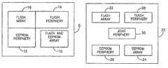
- FIGS. 1A and 1Billustrate two alternate embodiments of a single integrated circuit die, constructed and operative in accordance with the present invention.
- the present inventionincludes a die storing Flash and EEPROM bits.
- the bitsmay be stored together in the same array (as in FIG. 1A ) or in separate sections of the die (as in FIG. 1B ).
- FIG. 1Ashows a die 8 with a combined Flash and EEPROM array 10 and separate EEPROM and Flash peripheries 12 and 14 , respectively.
- EEPROM periphery 12may access and operate the EEPROM bits of array 10 while Flash periphery 14 may access and operate the Flash bits. Since some operations may be similar or the same for both EEPROM and Flash operation, there may exist a joint periphery 16 which may be used to access or to operate on both types of bits.
- FIG. 1Bshows a die 20 with separate arrays 22 and 24 for Flash bits and EEPROM bits, respectively. Similar to die 8 of FIG. 1A , there may be three kinds of peripheries: an EEPROM periphery 26 , a Flash periphery 28 and a joint periphery 30 .
- Charge pump circuitsused to generate voltages higher than the supply level, may be an example of peripheral circuits used to operate both the Flash and the EEPROM arrays.
- Sense amplifiersused to read out the array data, may be another example of joint peripheral circuits. In general, the ability to use common circuits to operate both types of arrays depends also on the specifications of the device. For example, if both arrays are allowed to be read at the same time, then the sense amplifiers can not be shared.
- FIGS. 1A and 1Bare exemplary in nature, the relative size and locations of the array(s) and peripheries will depend on the specific design and application of the chip. Furthermore, there may be more than one array of any type. Still further, the Flash bits may be block erased or page-mode erased, and similarly the EEPROM bits may be Byte or page erased.
- NROMnitride read only memory
- NROM cellsshown in FIGS. 2A and 2B to which reference is now made, may store data and may operate in arrays of either Flash or EEPROM types without any modification in the cell structure or in the operating mechanisms, as described hereinbelow.
- the NROM cellmay have a channel 100 between two diffusion areas 102 and 104 . Over the channel may be an oxide-nitride-oxide (ONO) sandwich (layers 109 , 110 and 111 ), wherein each layer is 100 or less thick, over which lies a gate 112 .
- ONOoxide-nitride-oxide
- chargemay be stored in a charge storage area 106 of nitride layer 110 near one of the diffusion areas 102 or 104 .
- charge storage area 106 of nitride layer 110near one of the diffusion areas 102 or 104 .
- chargemay be stored in a charge storage area 106 of nitride layer 110 near each of diffusion areas 102 and 104 .
- charge storage area 106 of nitride layer 110there may be two separated and separately chargeable areas 106 and 108 within nitride layer 110 , near each of diffusion areas 102 and 104
- Each chargeable areamay define one bit or multiple bits.
- each bitmay have only two distinct states, a ‘1’ and a ‘0’.
- each bitmay have multiple states. For example, for two bits per storage area, the four states are ‘11’, ‘00’, ‘10’ and ‘01’.
- single bitand ‘dual bit’ will be used to indicate storing charge in one or both of the charge storage areas 106 and 108 , irrespective of the number of threshold voltage levels defined for the storage area.
- the single and dual bit cells 30 and 40may be operated similarly, where the operations which occur to access the bit in charge area 106 in single bit cell 30 may also occur to access the bit in charge area 106 in dual bit cell 40 . Therefore, the presentation below will describe the dual bit operation; it being understood that the single bit operation may be similar but operative only on one of the bits, such as left bit 106 .
- gate 112may receive a high programming voltage V g
- left diffusion area 102may act as the drain and may receive a drain programming voltage VD
- right diffusion area 104may be grounded (i.e. area 104 acts as the source).
- the electronsmay flow from area 104 to area 102 (as indicated by arrow 114 ).
- the channel hot electronsmay then be injected into the nitride layer, in area 106 .
- the negative charge in area 106may raise the threshold voltage of the cell, if read in the reverse direction.
- the left diffusion area 102may be the source (i.e. grounded) and right diffusion area 104 may be the drain (i e. receives the drain programming voltage VD).
- the cellmay therefore be programmed in the opposite direction (as indicated by arrow 113 (FIG. 2 B)), and the electrons may then jump up into chargeable area 108 .
- a bitmay be read in the direction opposite (a “reverse read”) to that of its programming direction
- a reverse readis described in U.S. Pat. No. 6,011,725, mentioned above.
- right diffusion area 104may be the drain and left diffusion area 102 may be the source. This is known as the “read through” direction (indicated by arrow 113 ).
- the cellmay be read in the opposite direction (as indicated by arrow 114 ).
- left diffusion area 102may be the drain and right diffusion area 104 may be the source.
- the gatemay receive a negative erase gate voltage Vge, the left diffusion area 102 may receive an erase voltage V e and right diffusion area 104 may be left floating.
- the gatemay receive negative erase gate voltage Vge, the right diffusion area 104 may receive erase voltage Ve and left diffusion area 102 may be left floating
- the difference between an NROM EEPROM and an NROM flash devicemay not be in the structure of the cell nor much in the architecture of the array (particularly, there is no need for per cell select transistors as in floating gate EEPROM devices), but in the access operations (i.e. read, write and erase).
- the NROM cellmay be particularly suitable for multiple use chips.
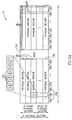
- FIG. 3illustrates an exemplary embodiment of independent flash array 22 and its programming and erase operations when implemented with NROM memory cells.
- the arraymay be a virtual ground array in which cells 116 are formed into a matrix.
- An exemplary architecture for such an arraymay be described in U.S. Ser. No. 09/727,781, filed Dec. 4, 2000, assigned to the common assignee of the present invention, whose disclosure is incorporated herein by reference. Alternative architectures are also incorporated in the present invention.
- Flash array 22may be segmented by select transistors 118 to implement blocks (sometimes also referred as “sectors” or “erase sectors”). Select transistors 118 may connect metal lines 120 to bit lines BL of a block.
- the Flash array 22may be further segmented by isolation zones 120 into isolated virtual ground slices.
- the isolation zones 122may be necessary to prevent interaction of two bits on the same WL that are accessed at the same time Isolation zones 122 may be manufactured as a thick oxide region, as a shallow trech isolation, as an unused column of memory cells or with any other suitable isolation technique.
- the bits of flash array 22may be individually read and programmed while blocks of the array may be erased together.
- two exemplary cells P and Qare noted.
- the gates of cells 116 of a rowmay be connected to a word line WL, such as WLA, and the diffusions of two columns of neighboring cells 116 may be connected together as a bit line BL, such as BLB.
- WLword line
- BLBbit line BL
- the right diffusion of cell P and the left diffusion of cell Qare connected to bit line BLB while their gates are connected to word line WLB
- Vr/0/Fmay indicate that the line may receive a read voltage Vr during reading, a 0 (or ground) voltage during programming and may be left floating (F), or driven to a low voltage, during erasure.
- a reading gate voltage Vgr(typically in the range of 2-5V, e.g. 3V) may be applied to word line WLB
- a read source voltage Vsr(typically in the range of approximately 1-2V, e.g. 1.5V) may be applied to bit line BLA
- bit line BLBmay be grounded (0V). All other bit lines may preferably be floated (FL) near ground prior to any operation (reading, programming or erasing). All other word lines may be grounded.
- a programming gate voltage Vgp(typically in the range of approximately 7-10V, e.g., 9V) may be applied to word line WLB
- a programming drain voltage Vdp(typically in the range of approximately 3-6V, e.g. 4.5V) may be applied to bit line BLB
- bit line BLAmay be grounded (0V). All other bit lines may preferably be floated (FL) near ground prior to any operation (programming or erasing). All other word lines may be grounded.
- a block of flash cellsare erased together, typically by erasing a column, some columns, or all columns of bits at a time.
- a negative erase gate voltage Vge(such as approximately in the range of ⁇ 2 to ⁇ 7V) may be applied to all word lines WL and a positive erase drain voltage Vde (typically in the range of approximately 3-6V, e.g. 4V) may be applied to the bit line whose bits need to be erased.
- bit lines BLB and BLDmay receive the positive erase drain voltage Vde
- the other bit lines of the arraymay be floating.
- bit line BLBThe bits on both sides of bit line BLB may be erased since both bits receive the exact same gate and bit line voltages.
- left-side bit 106 of cell Qmay also be erased together with right-side bit 108 of cell P and similarly for the other bits along bit line BLB
- bit lines BLsreceive the drain voltage Vd
- the considerations of how many bit lines may be erased togetherinclude erase time, erase characteristics, and erase currents.
- FIG. 4illustrates an exemplary embodiment of independent EEPROM array 24 and its programming and erase operations, when implemented with NROM memory cells.
- Such an exemplary arraymay be described in U.S. Ser. No. 09/761,818, filed Jan. 18, 2001 and Ser. No. 09/841,052, filed Apr. 25, 2001, assigned to the common assignee of the present invention, whose disclosure is incorporated herein by reference.
- EEPROM array 24may be implemented in blocks or not. The considerations for EEPROM array segmentation include operation performance and characteristics, disturbs, etc., as can be understood by those skilled in the art. The bits of EEPROM array 24 may be individually read, programmed and erased using the relevant read, program and erase voltages.
- EEPROM array 24may be similar to flash array 22 of FIG. 3 , with the addition of extra isolation zones 122 which define therebetween a slice of word lines and bit lines. Isolation zones 122 may serve to stop voltage propagation which may occur during programming and erasure and which may cause partial erasure of non-accessed cells. Depending on the array design and voltages used, the isolation zones 122 may divide the array into slices of a plurality of columns or of just one column.
- a programming gate voltage Vgp(typically in the range of approximately 7-10V, e.g., 9V) may be applied to word line WLB
- a programming drain voltage Vdp(typically in the range of approximately 3-6V, e.g. 4.5V) may be applied to bit line BLB
- bit line BLAmay be grounded (0V). All other bit lines may preferably be floated (FL) near ground prior to any operation (programming or erasing). All other word lines are either grounded or receive a programming inhibit voltage Vip, as described in U.S. Ser. No.
- the programming inhibit voltage Vipmay be 1V, although other inhibit voltages may be appropriate, as described in U.S. Ser. No. 09/761,818.
- a negative erase gate voltage Vge(such as approximately in the range of ⁇ 2V to ⁇ 7V) may be applied to word line WLB, a positive erase drain voltage Vde (typically in the range of approximately 3-5V, e.g. 4V) may be applied to bit line BLB, and the remaining bit lines are floated near ground before erasing. All other word lines receive an erase inhibit voltage Vie, as described in U.S. Ser. No. 09/761,818. For example, erase inhibit voltage Vie may be 3V, although other inhibit voltages may be appropriate, as described in U.S. Ser. No. 09/761,818.
- left-side bit 106 of cell Qmay receive the same gate, drain and source voltages. This means that left-side bit 106 of cell Q may also be erased together with right-side bit 108 of cell P. Accordingly, after an erasure of right-side bit 108 of cell P, left-side bit 106 of cell Q may be re-programmed to its original value. This is the case for a two-bit NROM cell. For single bit operation, it is preferable to arrange the bits so that they do not share a common bit line. In such an arrangement, no neighboring bit would be erased upon erasure of right-side bit 108 of cell P, for example.
- EEPROM array 24is not an emulated array as in the prior art but a proper EEPROM array. Each bit of the array is erasable directly and there is no need to copy the contents of a block to another storage area, modify them, erase the whole block and then rewrite the modified stored contents back into the array. Furthermore, it is also noted that the NROM based EEPROM array does not require a select transistor per cell as encountered in EEPROM arrays based on floating gate devices.
- the array architectures of NROM based EEPROM array 24 and Flash array 22may be identical or very similar. If desired, both arrays 22 and 24 may be implemented in slices. Alternatively, only EEPROM array 24 may be implemented in slices. A slice may be at least one column of NROM cells wide and the slices of the arrays may be of unequal widths.
- the operations of the two arraysmay also be very similar with the exception of the voltage levels that may vary between EEPROM and Flash operations in order to obtain different program and erase performance and characteristics.
- the access to the arraysmay differ in order to achieve the individual vs. group erasure. Since the NROM cell in the Flash and EEPROM arrays may be the same, and due to the identical or similar array architectures, the same array may be operated in either Flash or EEPROM modes
- the manufacturing processes to produce flash array 22 and EEPROM array 24may be identical or, at least, very similar. Moreover, the process to manufacture combined array 10 ( FIG. 1A ) may also be the same.
- An exemplary manufacturing process that may be used to manufacture both flash array 22 and EEPROM array 24is described in U.S. Pat. No. 6,297,096, assigned to the common assignee of the present invention, whose disclosure is incorporated herein by reference.
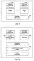
- FIG. 5Aillustrates an exemplary multiple use array 10 which may contain multiple physical sectors 130 , where each physical sector 130 may contain isolated virtual ground slices 132 .
- the physical sectors 130may be accessed by a single row decoder 134 and the data may be read with a sense amplifier 136 , one per set of isolated slices 132 .
- each physical sector 130may operate as a Flash or as an EEPROM type of array.
- the functionality of each physical sector 130may be predetermined, e g. by a pre-determined address mapping, or may be configurable. For example, the configuration may be performed through the decoding of the word line addresses
- Kthere are N physical sectors 130 of which K are Flash physical sectors and N-K are EEPROM physical sectors.
- Kmay be a predetermined number or a configurable number. If K is a configurable number, then additional peripheral circuits may need to be configured accordingly, e.g. the decoding circuitry, the address mapping generator, etc.
- Each physical sector 130may comprise multiple word lines WL while the global bit lines GBL may extend through multiple physical sectors 130 to the appropriate sense amplifier 136 .
- each sense amplifier 136may read data from Flash and EEPROM cells, depending on which word line, one part of a Flash or one part of an EEPROM physical sector, may be activated.
- FIGS. 5B and 5Cillustrate two embodiments of the array of FIG. 5A , using the array architecture of FIGS. 3 and 4 .
- FIG. 5Bshows two physical sectors 130 A and 130 B, where physical sector 130 A may be a Flash physical sector, with X word lines WL, and physical sector 130 B may be an EEPROM physical sector, with Y word lines WL.
- the two types of physical sectorsmay be generally identical with the only difference being their mode of operation.
- FIG. 5Calso shows two physical sectors, here labeled 130 C and 130 D, where physical sector 130 C may be a Flash physical sector, with X word lines WL, and physical sector 130 D may be an EEPROM physical sector, with Y word lines WL.
- the widths of the two types of slices 132may be different.
- Flash isolated slice 132 Ahas Q NROM cells while EEPROM isolated slices 132 B and 132 C have P NROM cells.
- different isolated virtual ground slices within a physical sectormay operate as Flash or EEPROM.
- the predetermined or configurable functionality of each sliceis controlled also by the BL decoder addresses.
- array 10may be a combined NROM based NOR Flash and EEPROM array. Such an array is described in U.S. Ser. No. 10/023,469, filed Dec. 20, 2001, assigned to the common assignee of the present invention, whose disclosure is incorporated herein by reference.
- the architecturemay be that of a NOR array, with one bit line BLj per column and a common line CLj per one or more word lines.
- Nor array 10 ′may be segmented by common line select transistors 140 and bit line select transistors 142 to implement blocks and to connect metal lines to bit lines BL and common lines CL of a block. It will be appreciated that the segmentation may be not required to practice the present invention, nor may the particular segmentation shown in FIG. 6 be the only segmentation possible.
- Each NROM cell 144may be connected between one bit line BLj and one column line CLj.
- each cellmay have two storage areas, a Flash storage area and an EEPROM storage area.
- the Flash storage areashown as a solid circle, may be the bit on the side of the cell connected to the common line CLj while the EEPROM storage area, shown as an open circle, may be on the side of the cell connected to the bit line BLj.
- a group of the Flash storage areas 144(such as those connected to a common line or all of the storage areas of a block) may be erased together while the EEPROM storage areas 142 may be individually erasable.
- a YMUX 150may include switching elements to connect the relevant power supplies to the relevant bit line BL and/or common lines CL.
- the voltages used for reading, programming and erasingmay be those described above with respect to FIGS. 3 and 4 , where those for FIG. 3 may be appropriate for the Flash storage area and those for FIG. 4 may be appropriate for the EEPROM storage area.
- the terminal close to the storage area being readmay be grounded.
- Each type of bitmay be read differently.
- the Flash storage areamay be read with a CL sense amplifier 146 , which may perform a close to ground sensing, while the EEPROM storage area may be read with a BL sense amplifier 148 , which may perform a standard, precharge sensing. More details about implementing close to ground reading can be found in U.S. Pat. No. 6,128,226, whose disclosure is incorporated herein by reference.
- YMUX 150may connect the relevant sense amplifier to be line BL depending on which type of bit is to be read at a given time.
- the terminal close to the storage area being programmed or erasedmay be at programming or erasing voltages Vdp or Vde.
- Flash storage areas of a blockmay be erased together.
- the common lines CL of the blockmay be driven to the erase voltage Ve
- all of the bit lines BL of the blockmay be set to float and the word lines WL of the block may be driven to their erase voltage.
- a ⁇ 7V erase voltagecan be used. Positive erase voltages can be utilized as well.
- the NOR arraymay be utilized for multiple die 20 ( FIG. 1B ).
- the NROM cellsmay be utilized as single or as dual bit cells, where the bits may be flash bits. The storage areas connected to one common line may be erased together and the storage areas connected to one bit line may be erased together.
- the NROM cellsmay be single bit cells which may use the EEPROM storage areas (i.e. those connected to bit lines BLj).
- the bits stored thereinmay be EEPROM bits that are accessed as described hereinabove.
- FIGS. 7 and 7Aillustrate a multiple use die with more than one array of at least one type.
- the general casemay be shown in FIG. 7 which a specific case may be shown in FIG. 7A .
- the present inventionmay be used for N arrays on a single die, where some of the N arrays may be Flash type arrays and some of the arrays may be EEPROM type arrays.
- FIG. 7Ashows one embodiment with two Flash arrays 164 and 166 and one EEPROM array 168 .
- Flash array 164may be a word mode array, in which words of a fixed length may be erased at a time, useful for storing program code which changes rarely and may be read and programmed in small chunks but erased in large chunks. Flash array 164 may have a fast access time.
- Flash array 166may be a page mode array, in which entire pages or blocks may be erased at a time, useful for storing large amounts of data, such as a video sequence. Such an array may have long first byte latency and fast burst access.
- EEPROM array 168may have individual byte or word erasure, useful for storing small chunks of data that may be frequently modified (e.g. phone numbers on a cellular telephone).
Landscapes
- Engineering & Computer Science (AREA)
- Computer Hardware Design (AREA)
- Microelectronics & Electronic Packaging (AREA)
- Non-Volatile Memory (AREA)
- Semiconductor Memories (AREA)
- Read Only Memory (AREA)
Abstract
Description
Claims (20)
Priority Applications (3)
| Application Number | Priority Date | Filing Date | Title |
|---|---|---|---|
| US11/246,193US7738304B2 (en) | 2002-07-10 | 2005-10-11 | Multiple use memory chip |
| US11/979,184US7489562B2 (en) | 2002-07-10 | 2007-10-31 | Multiple use memory chip |
| US11/979,182US7573745B2 (en) | 2002-07-10 | 2007-10-31 | Multiple use memory chip |
Applications Claiming Priority (3)
| Application Number | Priority Date | Filing Date | Title |
|---|---|---|---|
| US10/191,451US6917544B2 (en) | 2002-07-10 | 2002-07-10 | Multiple use memory chip |
| US11/024,750US6954382B2 (en) | 2002-07-10 | 2004-12-30 | Multiple use memory chip |
| US11/246,193US7738304B2 (en) | 2002-07-10 | 2005-10-11 | Multiple use memory chip |
Related Parent Applications (1)
| Application Number | Title | Priority Date | Filing Date |
|---|---|---|---|
| US11/024,750ContinuationUS6954382B2 (en) | 2002-07-10 | 2004-12-30 | Multiple use memory chip |
Related Child Applications (2)
| Application Number | Title | Priority Date | Filing Date |
|---|---|---|---|
| US11/979,182ContinuationUS7573745B2 (en) | 2002-07-10 | 2007-10-31 | Multiple use memory chip |
| US11/979,184ContinuationUS7489562B2 (en) | 2002-07-10 | 2007-10-31 | Multiple use memory chip |
Publications (2)
| Publication Number | Publication Date |
|---|---|
| US20060152975A1 US20060152975A1 (en) | 2006-07-13 |
| US7738304B2true US7738304B2 (en) | 2010-06-15 |
Family
ID=29735291
Family Applications (5)
| Application Number | Title | Priority Date | Filing Date |
|---|---|---|---|
| US10/191,451Expired - LifetimeUS6917544B2 (en) | 2002-07-10 | 2002-07-10 | Multiple use memory chip |
| US11/024,750Expired - LifetimeUS6954382B2 (en) | 2002-07-10 | 2004-12-30 | Multiple use memory chip |
| US11/246,193Expired - LifetimeUS7738304B2 (en) | 2002-07-10 | 2005-10-11 | Multiple use memory chip |
| US11/979,184Expired - LifetimeUS7489562B2 (en) | 2002-07-10 | 2007-10-31 | Multiple use memory chip |
| US11/979,182Expired - LifetimeUS7573745B2 (en) | 2002-07-10 | 2007-10-31 | Multiple use memory chip |
Family Applications Before (2)
| Application Number | Title | Priority Date | Filing Date |
|---|---|---|---|
| US10/191,451Expired - LifetimeUS6917544B2 (en) | 2002-07-10 | 2002-07-10 | Multiple use memory chip |
| US11/024,750Expired - LifetimeUS6954382B2 (en) | 2002-07-10 | 2004-12-30 | Multiple use memory chip |
Family Applications After (2)
| Application Number | Title | Priority Date | Filing Date |
|---|---|---|---|
| US11/979,184Expired - LifetimeUS7489562B2 (en) | 2002-07-10 | 2007-10-31 | Multiple use memory chip |
| US11/979,182Expired - LifetimeUS7573745B2 (en) | 2002-07-10 | 2007-10-31 | Multiple use memory chip |
Country Status (4)
| Country | Link |
|---|---|
| US (5) | US6917544B2 (en) |
| EP (1) | EP1381055A3 (en) |
| JP (1) | JP2004039233A (en) |
| IL (1) | IL156854A0 (en) |
Cited By (4)
| Publication number | Priority date | Publication date | Assignee | Title |
|---|---|---|---|---|
| US20090251954A1 (en)* | 2008-04-08 | 2009-10-08 | Samsung Electronics Co., Ltd. | Variable resistance memory device and system |
| US8471328B2 (en) | 2010-07-26 | 2013-06-25 | United Microelectronics Corp. | Non-volatile memory and manufacturing method thereof |
| US20140063957A1 (en)* | 2011-12-02 | 2014-03-06 | Tsinghua University | Nor flash memory array structure, mixed nonvolatile flash memory and memory system comprising the same |
| US9171846B2 (en) | 2012-05-31 | 2015-10-27 | Moon J. Kim | Leakage and performance graded memory |
Families Citing this family (64)
| Publication number | Priority date | Publication date | Assignee | Title |
|---|---|---|---|---|
| US6768165B1 (en) | 1997-08-01 | 2004-07-27 | Saifun Semiconductors Ltd. | Two bit non-volatile electrically erasable and programmable semiconductor memory cell utilizing asymmetrical charge trapping |
| US6614692B2 (en) | 2001-01-18 | 2003-09-02 | Saifun Semiconductors Ltd. | EEPROM array and method for operation thereof |
| US6584017B2 (en) | 2001-04-05 | 2003-06-24 | Saifun Semiconductors Ltd. | Method for programming a reference cell |
| US6700818B2 (en) | 2002-01-31 | 2004-03-02 | Saifun Semiconductors Ltd. | Method for operating a memory device |
| US7190620B2 (en)* | 2002-01-31 | 2007-03-13 | Saifun Semiconductors Ltd. | Method for operating a memory device |
| US6917544B2 (en)* | 2002-07-10 | 2005-07-12 | Saifun Semiconductors Ltd. | Multiple use memory chip |
| US7136304B2 (en) | 2002-10-29 | 2006-11-14 | Saifun Semiconductor Ltd | Method, system and circuit for programming a non-volatile memory array |
| US6992932B2 (en) | 2002-10-29 | 2006-01-31 | Saifun Semiconductors Ltd | Method circuit and system for read error detection in a non-volatile memory array |
| US6963505B2 (en)* | 2002-10-29 | 2005-11-08 | Aifun Semiconductors Ltd. | Method circuit and system for determining a reference voltage |
| US6967896B2 (en)* | 2003-01-30 | 2005-11-22 | Saifun Semiconductors Ltd | Address scramble |
| US7178004B2 (en) | 2003-01-31 | 2007-02-13 | Yan Polansky | Memory array programming circuit and a method for using the circuit |
| US7142464B2 (en) | 2003-04-29 | 2006-11-28 | Saifun Semiconductors Ltd. | Apparatus and methods for multi-level sensing in a memory array |
| US7057928B2 (en)* | 2003-07-08 | 2006-06-06 | Hewlett-Packard Development Company, L.P. | System and method for erasing high-density non-volatile fast memory |
| US7123532B2 (en) | 2003-09-16 | 2006-10-17 | Saifun Semiconductors Ltd. | Operating array cells with matched reference cells |
| WO2005094178A2 (en) | 2004-04-01 | 2005-10-13 | Saifun Semiconductors Ltd. | Method, circuit and systems for erasing one or more non-volatile memory cells |
| US7158411B2 (en)* | 2004-04-01 | 2007-01-02 | Macronix International Co., Ltd. | Integrated code and data flash memory |
| US7755938B2 (en)* | 2004-04-19 | 2010-07-13 | Saifun Semiconductors Ltd. | Method for reading a memory array with neighbor effect cancellation |
| JP2005322109A (en) | 2004-05-11 | 2005-11-17 | Renesas Technology Corp | Ic card module |
| US7366025B2 (en)* | 2004-06-10 | 2008-04-29 | Saifun Semiconductors Ltd. | Reduced power programming of non-volatile cells |
| US7317633B2 (en) | 2004-07-06 | 2008-01-08 | Saifun Semiconductors Ltd | Protection of NROM devices from charge damage |
| US7095655B2 (en)* | 2004-08-12 | 2006-08-22 | Saifun Semiconductors Ltd. | Dynamic matching of signal path and reference path for sensing |
| US20060036803A1 (en)* | 2004-08-16 | 2006-02-16 | Mori Edan | Non-volatile memory device controlled by a micro-controller |
| US7638850B2 (en) | 2004-10-14 | 2009-12-29 | Saifun Semiconductors Ltd. | Non-volatile memory structure and method of fabrication |
| US7262999B2 (en)* | 2004-11-24 | 2007-08-28 | Macronix International Co., Ltd. | System and method for preventing read margin degradation for a memory array |
| JP4628757B2 (en)* | 2004-11-26 | 2011-02-09 | イノテック株式会社 | Semiconductor memory device |
| US7257025B2 (en)* | 2004-12-09 | 2007-08-14 | Saifun Semiconductors Ltd | Method for reading non-volatile memory cells |
| EP1686592A3 (en) | 2005-01-19 | 2007-04-25 | Saifun Semiconductors Ltd. | Partial erase verify |
| US8053812B2 (en) | 2005-03-17 | 2011-11-08 | Spansion Israel Ltd | Contact in planar NROM technology |
| US8400841B2 (en) | 2005-06-15 | 2013-03-19 | Spansion Israel Ltd. | Device to program adjacent storage cells of different NROM cells |
| US7184313B2 (en) | 2005-06-17 | 2007-02-27 | Saifun Semiconductors Ltd. | Method circuit and system for compensating for temperature induced margin loss in non-volatile memory cells |
| US7786512B2 (en) | 2005-07-18 | 2010-08-31 | Saifun Semiconductors Ltd. | Dense non-volatile memory array and method of fabrication |
| US7668017B2 (en) | 2005-08-17 | 2010-02-23 | Saifun Semiconductors Ltd. | Method of erasing non-volatile memory cells |
| US8116142B2 (en)* | 2005-09-06 | 2012-02-14 | Infineon Technologies Ag | Method and circuit for erasing a non-volatile memory cell |
| US7881123B2 (en)* | 2005-09-23 | 2011-02-01 | Macronix International Co., Ltd. | Multi-operation mode nonvolatile memory |
| US7221138B2 (en) | 2005-09-27 | 2007-05-22 | Saifun Semiconductors Ltd | Method and apparatus for measuring charge pump output current |
| JP4892215B2 (en)* | 2005-09-28 | 2012-03-07 | 富士通セミコンダクター株式会社 | Semiconductor memory device |
| US7511333B2 (en) | 2005-10-06 | 2009-03-31 | Promos Technologies Inc. | Nonvolatile memory cell with multiple floating gates and a connection region in the channel |
| US7352627B2 (en) | 2006-01-03 | 2008-04-01 | Saifon Semiconductors Ltd. | Method, system, and circuit for operating a non-volatile memory array |
| US7808818B2 (en) | 2006-01-12 | 2010-10-05 | Saifun Semiconductors Ltd. | Secondary injection for NROM |
| US8253452B2 (en) | 2006-02-21 | 2012-08-28 | Spansion Israel Ltd | Circuit and method for powering up an integrated circuit and an integrated circuit utilizing same |
| US7760554B2 (en) | 2006-02-21 | 2010-07-20 | Saifun Semiconductors Ltd. | NROM non-volatile memory and mode of operation |
| US7692961B2 (en) | 2006-02-21 | 2010-04-06 | Saifun Semiconductors Ltd. | Method, circuit and device for disturb-control of programming nonvolatile memory cells by hot-hole injection (HHI) and by channel hot-electron (CHE) injection |
| US7638835B2 (en) | 2006-02-28 | 2009-12-29 | Saifun Semiconductors Ltd. | Double density NROM with nitride strips (DDNS) |
| US7701779B2 (en) | 2006-04-27 | 2010-04-20 | Sajfun Semiconductors Ltd. | Method for programming a reference cell |
| US7605579B2 (en) | 2006-09-18 | 2009-10-20 | Saifun Semiconductors Ltd. | Measuring and controlling current consumption and output current of charge pumps |
| US7710777B1 (en)* | 2006-12-20 | 2010-05-04 | Marvell International Ltd. | Semi-volatile NAND flash memory |
| WO2008113033A1 (en)* | 2007-03-14 | 2008-09-18 | Slacker, Inc. | Systems and methods of utilizing multiple satellite transponders for data distribution |
| US7613042B2 (en)* | 2007-11-05 | 2009-11-03 | Spansion Llc | Decoding system capable of reducing sector select area overhead for flash memory |
| US7590001B2 (en) | 2007-12-18 | 2009-09-15 | Saifun Semiconductors Ltd. | Flash memory with optimized write sector spares |
| US20090171650A1 (en)* | 2007-12-27 | 2009-07-02 | Unity Semiconductor Corporation | Non-Volatile memories in interactive entertainment systems |
| US7645993B2 (en)* | 2007-12-28 | 2010-01-12 | Spansion, Llc | Arrayed neutron detector with multi shielding allowing for discrimination between radiation types |
| US7826267B2 (en)* | 2008-05-23 | 2010-11-02 | Silicon Storage Technology, Inc. | Method and apparatus for reading and programming a non-volatile memory cell in a virtual ground array |
| JP2010033682A (en)* | 2008-07-31 | 2010-02-12 | Panasonic Corp | Nonvolatile semiconductor memory device |
| JP5086933B2 (en)* | 2008-08-06 | 2012-11-28 | 株式会社東芝 | Driving method of nonvolatile semiconductor memory device |
| CN102693905B (en)* | 2011-03-22 | 2015-08-05 | 中芯国际集成电路制造(上海)有限公司 | The formation method of flash cell and floating boom thereof |
| US20130056641A1 (en)* | 2011-09-01 | 2013-03-07 | Massachusetts Institute Of Technology | Solid-state neutron detector with gadolinium converter |
| CN102544022B (en)* | 2012-01-05 | 2014-10-22 | 清华大学 | Hybrid non-volatile flash memory and memory system thereof |
| TWI494930B (en)* | 2012-05-03 | 2015-08-01 | Macronix Int Co Ltd | Plural operation of memory device |
| US9430339B1 (en) | 2012-12-27 | 2016-08-30 | Marvell International Ltd. | Method and apparatus for using wear-out blocks in nonvolatile memory |
| WO2015131029A1 (en)* | 2014-02-28 | 2015-09-03 | Sun Chemical Corporation | Radiation curable inks and coatings containing diacetone acrylamide |
| TWI626658B (en)* | 2016-06-14 | 2018-06-11 | 旺宏電子股份有限公司 | Memory device and operating method thereof |
| CN108509154B (en)* | 2018-03-31 | 2021-07-13 | 深圳忆联信息系统有限公司 | Method and device for dynamically recombining raid according to bad block distribution |
| JP2019220242A (en)* | 2018-06-21 | 2019-12-26 | セイコーエプソン株式会社 | Non-volatile storage device, microcomputer, and electronic apparatus |
| US20240402006A1 (en)* | 2023-06-02 | 2024-12-05 | International Business Machines Corporation | Flexible ultraviolet sensor |
Citations (530)
| Publication number | Priority date | Publication date | Assignee | Title |
|---|---|---|---|---|
| GB1297899A (en) | 1970-10-02 | 1972-11-29 | ||
| US3881180A (en) | 1971-11-30 | 1975-04-29 | Texas Instruments Inc | Non-volatile memory cell |
| US3895360A (en) | 1974-01-29 | 1975-07-15 | Westinghouse Electric Corp | Block oriented random access memory |
| US3952325A (en) | 1971-07-28 | 1976-04-20 | U.S. Philips Corporation | Semiconductor memory elements |
| US4016588A (en) | 1974-12-27 | 1977-04-05 | Nippon Electric Company, Ltd. | Non-volatile semiconductor memory device |
| US4017888A (en) | 1975-12-31 | 1977-04-12 | International Business Machines Corporation | Non-volatile metal nitride oxide semiconductor device |
| US4145703A (en) | 1977-04-15 | 1979-03-20 | Supertex, Inc. | High power MOS device and fabrication method therefor |
| US4151021A (en) | 1977-01-26 | 1979-04-24 | Texas Instruments Incorporated | Method of making a high density floating gate electrically programmable ROM |
| US4173791A (en) | 1977-09-16 | 1979-11-06 | Fairchild Camera And Instrument Corporation | Insulated gate field-effect transistor read-only memory array |
| US4173766A (en) | 1977-09-16 | 1979-11-06 | Fairchild Camera And Instrument Corporation | Insulated gate field-effect transistor read-only memory cell |
| US4247861A (en) | 1979-03-09 | 1981-01-27 | Rca Corporation | High performance electrically alterable read-only memory (EAROM) |
| US4257832A (en) | 1978-07-24 | 1981-03-24 | Siemens Aktiengesellschaft | Process for producing an integrated multi-layer insulator memory cell |
| US4281397A (en) | 1979-10-29 | 1981-07-28 | Texas Instruments Incorporated | Virtual ground MOS EPROM or ROM matrix |
| US4306353A (en) | 1979-06-13 | 1981-12-22 | Siemens Aktiengesellschaft | Process for production of integrated MOS circuits with and without MNOS memory transistors in silicon-gate technology |
| US4342102A (en) | 1980-06-18 | 1982-07-27 | Signetics Corporation | Semiconductor memory array |
| US4342149A (en) | 1979-11-23 | 1982-08-03 | Siemens Aktiengesellschaft | Method of making very short channel length MNOS and MOS devices by double implantation of one conductivity type subsequent to other type implantation |
| US4360900A (en) | 1978-11-27 | 1982-11-23 | Texas Instruments Incorporated | Non-volatile semiconductor memory elements |
| US4373248A (en) | 1978-07-12 | 1983-02-15 | Texas Instruments Incorporated | Method of making high density semiconductor device such as floating gate electrically programmable ROM or the like |
| US4380057A (en) | 1980-10-27 | 1983-04-12 | International Business Machines Corporation | Electrically alterable double dense memory |
| US4388705A (en) | 1981-10-01 | 1983-06-14 | Mostek Corporation | Semiconductor memory circuit |
| US4389705A (en) | 1981-08-21 | 1983-06-21 | Mostek Corporation | Semiconductor memory circuit with depletion data transfer transistor |
| US4404747A (en) | 1981-07-29 | 1983-09-20 | Schur, Inc. | Knife and sheath assembly |
| US4435786A (en) | 1981-11-23 | 1984-03-06 | Fairchild Camera And Instrument Corporation | Self-refreshing memory cell |
| US4448400A (en) | 1981-07-13 | 1984-05-15 | Eliyahou Harari | Highly scalable dynamic RAM cell with self-signal amplification |
| US4471373A (en) | 1980-02-27 | 1984-09-11 | Hitachi, Ltd. | Semiconductor integrated circuit device with memory MISFETS and thin and thick gate insulator MISFETS |
| US4494016A (en) | 1982-07-26 | 1985-01-15 | Sperry Corporation | High performance MESFET transistor for VLSI implementation |
| US4507673A (en) | 1979-10-13 | 1985-03-26 | Tokyo Shibaura Denki Kabushiki Kaisha | Semiconductor memory device |
| US4521796A (en) | 1980-12-11 | 1985-06-04 | General Instrument Corporation | Memory implant profile for improved channel shielding in electrically alterable read only memory semiconductor device |
| US4527257A (en) | 1982-08-25 | 1985-07-02 | Westinghouse Electric Corp. | Common memory gate non-volatile transistor memory |
| GB2157489A (en) | 1984-03-23 | 1985-10-23 | Hitachi Ltd | A semiconductor integrated circuit memory device |
| US4586163A (en) | 1982-09-13 | 1986-04-29 | Toshiba Shibaura Denki Kabushiki Kaisha | Multi-bit-per-cell read only memory circuit |
| US4613956A (en) | 1983-02-23 | 1986-09-23 | Texas Instruments Incorporated | Floating gate memory with improved dielectric |
| US4630085A (en) | 1984-02-28 | 1986-12-16 | Nec Corporation | Erasable, programmable read-only memory device |
| US4663645A (en) | 1984-05-23 | 1987-05-05 | Hitachi, Ltd. | Semiconductor device of an LDD structure having a floating gate |
| US4665426A (en) | 1985-02-01 | 1987-05-12 | Advanced Micro Devices, Inc. | EPROM with ultraviolet radiation transparent silicon nitride passivation layer |
| US4667217A (en) | 1985-04-19 | 1987-05-19 | Ncr Corporation | Two bit vertically/horizontally integrated memory cell |
| US4672409A (en) | 1980-12-25 | 1987-06-09 | Fujitsu Limited | Nonvolatile semiconductor memory device |
| US4725984A (en) | 1984-02-21 | 1988-02-16 | Seeq Technology, Inc. | CMOS eprom sense amplifier |
| US4733105A (en) | 1985-09-04 | 1988-03-22 | Oki Electric Industry Co., Ltd. | CMOS output circuit |
| US4742491A (en) | 1985-09-26 | 1988-05-03 | Advanced Micro Devices, Inc. | Memory cell having hot-hole injection erase mode |
| US4758869A (en) | 1986-08-29 | 1988-07-19 | Waferscale Integration, Inc. | Nonvolatile floating gate transistor structure |
| US4760555A (en) | 1986-04-21 | 1988-07-26 | Texas Instruments Incorporated | Memory array with an array reorganizer |
| US4761764A (en) | 1985-04-18 | 1988-08-02 | Nec Corporation | Programmable read only memory operable with reduced programming power consumption |
| US4769340A (en) | 1983-11-28 | 1988-09-06 | Exel Microelectronics, Inc. | Method for making electrically programmable memory device by doping the floating gate by implant |
| US4780424A (en) | 1987-09-28 | 1988-10-25 | Intel Corporation | Process for fabricating electrically alterable floating gate memory devices |
| US4839705A (en) | 1987-12-16 | 1989-06-13 | Texas Instruments Incorporated | X-cell EEPROM array |
| US4847808A (en) | 1986-04-22 | 1989-07-11 | Nec Corporation | Read only semiconductor memory having multiple bit cells |
| US4857770A (en) | 1988-02-29 | 1989-08-15 | Advanced Micro Devices, Inc. | Output buffer arrangement for reducing chip noise without speed penalty |
| US4870470A (en) | 1987-10-16 | 1989-09-26 | International Business Machines Corporation | Non-volatile memory cell having Si rich silicon nitride charge trapping layer |
| US4888735A (en) | 1987-12-30 | 1989-12-19 | Elite Semiconductor & Systems Int'l., Inc. | ROM cell and array configuration |
| US4916671A (en) | 1988-09-06 | 1990-04-10 | Mitsubishi Denki Kabushiki Kaisha | Semiconductor memory device having sense amplifier having improved activation timing thereof and operating method thereof |
| US4941028A (en) | 1988-08-10 | 1990-07-10 | Actel Corporation | Structure for protecting thin dielectrics during processing |
| US4961010A (en) | 1989-05-19 | 1990-10-02 | National Semiconductor Corporation | Output buffer for reducing switching induced noise |
| US4992391A (en) | 1989-11-29 | 1991-02-12 | Advanced Micro Devices, Inc. | Process for fabricating a control gate for a floating gate FET |
| US5021999A (en) | 1987-12-17 | 1991-06-04 | Mitsubishi Denki Kabushiki Kaisha | Non-volatile semiconductor memory device with facility of storing tri-level data |
| US5027321A (en) | 1989-11-21 | 1991-06-25 | Intel Corporation | Apparatus and method for improved reading/programming of virtual ground EPROM arrays |
| US5029063A (en) | 1989-03-25 | 1991-07-02 | Eurosil Electronic Gmbh | MOSFET multiplying circuit |
| US5042009A (en) | 1988-12-09 | 1991-08-20 | Waferscale Integration, Inc. | Method for programming a floating gate memory device |
| US5075245A (en) | 1990-08-03 | 1991-12-24 | Intel Corporation | Method for improving erase characteristics of buried bit line flash EPROM devices without using sacrificial oxide growth and removal steps |
| US5081371A (en) | 1990-11-07 | 1992-01-14 | U.S. Philips Corp. | Integrated charge pump circuit with back bias voltage reduction |
| US5086325A (en) | 1990-11-21 | 1992-02-04 | Atmel Corporation | Narrow width EEPROM with single diffusion electrode formation |
| US5094968A (en) | 1990-11-21 | 1992-03-10 | Atmel Corporation | Fabricating a narrow width EEPROM with single diffusion electrode formation |
| US5104819A (en) | 1989-08-07 | 1992-04-14 | Intel Corporation | Fabrication of interpoly dielctric for EPROM-related technologies |
| US5117389A (en) | 1990-09-05 | 1992-05-26 | Macronix International Co., Ltd. | Flat-cell read-only-memory integrated circuit |
| US5120672A (en) | 1989-02-22 | 1992-06-09 | Texas Instruments Incorporated | Fabricating a single level merged EEPROM cell having an ONO memory stack substantially spaced from the source region |
| US5142496A (en) | 1991-06-03 | 1992-08-25 | Advanced Micro Devices, Inc. | Method for measuring VT 's less than zero without applying negative voltages |
| US5142495A (en) | 1989-03-10 | 1992-08-25 | Intel Corporation | Variable load for margin mode |
| US5159570A (en) | 1987-12-22 | 1992-10-27 | Texas Instruments Incorporated | Four memory state EEPROM |
| US5168334A (en) | 1987-07-31 | 1992-12-01 | Texas Instruments, Incorporated | Non-volatile semiconductor memory |
| US5172338A (en) | 1989-04-13 | 1992-12-15 | Sundisk Corporation | Multi-state EEprom read and write circuits and techniques |
| US5175120A (en) | 1991-10-11 | 1992-12-29 | Micron Technology, Inc. | Method of processing a semiconductor wafer to form an array of nonvolatile memory devices employing floating gate transistors and peripheral area having CMOS transistors |
| US5204835A (en) | 1990-06-13 | 1993-04-20 | Waferscale Integration Inc. | Eprom virtual ground array |
| US5214303A (en) | 1991-02-08 | 1993-05-25 | Sharp Kabushiki Kaisha | Semiconductor device ROM having an offset region |
| US5237213A (en) | 1991-04-15 | 1993-08-17 | Oki Electric Industry Co., Ltd. | Semiconductor integrated circuit with low-noise output buffers |
| US5241497A (en) | 1990-06-14 | 1993-08-31 | Creative Integrated Systems, Inc. | VLSI memory with increased memory access speed, increased memory cell density and decreased parasitic capacitance |
| US5260593A (en) | 1991-12-10 | 1993-11-09 | Micron Technology, Inc. | Semiconductor floating gate device having improved channel-floating gate interaction |
| US5268861A (en) | 1991-04-10 | 1993-12-07 | Sharp Kabushiki Kaisha | Semiconductor read only memory |
| US5276646A (en) | 1990-09-25 | 1994-01-04 | Samsung Electronics Co., Ltd. | High voltage generating circuit for a semiconductor memory circuit |
| US5280420A (en) | 1992-10-02 | 1994-01-18 | National Semiconductor Corporation | Charge pump which operates on a low voltage power supply |
| US5289412A (en) | 1992-06-19 | 1994-02-22 | Intel Corporation | High-speed bias-stabilized current-mirror referencing circuit for non-volatile memories |
| US5293563A (en) | 1988-12-29 | 1994-03-08 | Sharp Kabushiki Kaisha | Multi-level memory cell with increased read-out margin |
| US5295092A (en) | 1992-01-21 | 1994-03-15 | Sharp Kabushiki Kaisha | Semiconductor read only memory |
| US5295108A (en) | 1992-04-08 | 1994-03-15 | Nec Corporation | Electrically erasable and programmable read only memory device with simple controller for selecting operational sequences after confirmation |
| US5305262A (en) | 1991-09-11 | 1994-04-19 | Kawasaki Steel Corporation | Semiconductor integrated circuit |
| US5311049A (en) | 1991-10-17 | 1994-05-10 | Rohm Co., Ltd. | Non-volatile semiconductor memory with outer drain diffusion layer |
| US5315541A (en) | 1992-07-24 | 1994-05-24 | Sundisk Corporation | Segmented column memory array |
| US5324675A (en) | 1992-03-31 | 1994-06-28 | Kawasaki Steel Corporation | Method of producing semiconductor devices of a MONOS type |
| US5335198A (en) | 1993-05-06 | 1994-08-02 | Advanced Micro Devices, Inc. | Flash EEPROM array with high endurance |
| US5334555A (en) | 1991-11-06 | 1994-08-02 | Sony Corporation | Method of determining conditions for plasma silicon nitride film growth and method of manufacturing semiconductor device |
| US5338954A (en) | 1991-10-31 | 1994-08-16 | Rohm Co., Ltd. | Semiconductor memory device having an insulating film and a trap film joined in a channel region |
| US5345425A (en) | 1990-11-20 | 1994-09-06 | Fujitsu Limited | Semiconductor memory device |
| US5349221A (en) | 1991-10-25 | 1994-09-20 | Rohm Co., Ltd. | Semiconductor memory device and method of reading out information for the same |
| US5350710A (en) | 1993-06-24 | 1994-09-27 | United Microelectronics Corporation | Device for preventing antenna effect on circuit |
| US5352620A (en) | 1984-05-23 | 1994-10-04 | Hitachi, Ltd. | Method of making semiconductor device with memory cells and peripheral transistors |
| US5357134A (en) | 1991-10-31 | 1994-10-18 | Rohm Co., Ltd. | Nonvolatile semiconductor device having charge trap film containing silicon crystal grains |
| US5359554A (en) | 1991-08-27 | 1994-10-25 | Matsushita Electric Industrial Co., Ltd. | Semiconductor memory device having an energy gap for high speed operation |
| US5361343A (en) | 1991-07-30 | 1994-11-01 | Intel Corporation | Microprocessor system including first and second nonvolatile memory arrays which may be simultaneously read and reprogrammed |
| US5366915A (en) | 1992-08-28 | 1994-11-22 | Nec Corporation | Process of fabricating floating gate type field effect transistor having drain region gently varied in impurity profile |
| US5375094A (en) | 1992-06-19 | 1994-12-20 | Kabushiki Kaisha Toshiba | Nonvolatile semiconductor memory system with a plurality of erase blocks |
| US5381374A (en) | 1992-01-09 | 1995-01-10 | Kabushiki Kaisha Toshiba | Memory cell data output circuit having improved access time |
| US5393701A (en) | 1993-04-08 | 1995-02-28 | United Microelectronics Corporation | Layout design to eliminate process antenna effect |
| US5394355A (en) | 1990-08-28 | 1995-02-28 | Mitsubishi Denki Kabushiki Kaisha | Read only memory for storing multi-data |
| US5399891A (en) | 1992-01-22 | 1995-03-21 | Macronix International Co., Ltd. | Floating gate or flash EPROM transistor array having contactless source and drain diffusions |
| US5400286A (en) | 1993-08-17 | 1995-03-21 | Catalyst Semiconductor Corp. | Self-recovering erase scheme to enhance flash memory endurance |
| US5402374A (en) | 1993-04-30 | 1995-03-28 | Rohm Co., Ltd. | Non-volatile semiconductor memory device and memory circuit using the same |
| US5412601A (en) | 1992-08-31 | 1995-05-02 | Nippon Steel Corporation | Non-volatile semiconductor memory device capable of storing multi-value data in each memory cell |
| US5414693A (en) | 1991-08-29 | 1995-05-09 | Hyundai Electronics Industries Co., Ltd. | Self-aligned dual-bit split gate (DSG) flash EEPROM cell |
| US5418176A (en) | 1994-02-17 | 1995-05-23 | United Microelectronics Corporation | Process for producing memory devices having narrow buried N+ lines |
| US5418743A (en) | 1992-12-07 | 1995-05-23 | Nippon Steel Corporation | Method of writing into non-volatile semiconductor memory |
| US5422844A (en) | 1992-12-21 | 1995-06-06 | National Semiconductor Corporation | Memory array with field oxide islands eliminated and method |
| US5424978A (en) | 1993-03-15 | 1995-06-13 | Nippon Steel Corporation | Non-volatile semiconductor memory cell capable of storing more than two different data and method of using the same |
| US5424567A (en) | 1991-05-15 | 1995-06-13 | North American Philips Corporation | Protected programmable transistor with reduced parasitic capacitances and method of fabrication |
| US5426605A (en) | 1992-08-19 | 1995-06-20 | U.S. Philips Corporation | Semiconductor memory device |
| US5434825A (en) | 1988-06-08 | 1995-07-18 | Harari; Eliyahou | Flash EEPROM system cell array with more than two storage states per memory cell |
| US5436478A (en) | 1994-03-16 | 1995-07-25 | National Semiconductor Corporation | Fast access AMG EPROM with segment select transistors which have an increased width |
| US5436481A (en) | 1993-01-21 | 1995-07-25 | Nippon Steel Corporation | MOS-type semiconductor device and method of making the same |
| US5440505A (en) | 1994-01-21 | 1995-08-08 | Intel Corporation | Method and circuitry for storing discrete amounts of charge in a single memory element |
| US5450341A (en) | 1992-08-31 | 1995-09-12 | Nippon Steel Corporation | Non-volatile semiconductor memory device having memory cells, each for at least three different data writable thereinto selectively and a method of using the same |
| US5450354A (en) | 1992-08-31 | 1995-09-12 | Nippon Steel Corporation | Non-volatile semiconductor memory device detachable deterioration of memory cells |
| US5455793A (en) | 1992-01-15 | 1995-10-03 | National Semiconductor Corp. | Electrically reprogrammable EPROM cell with merged transistor and optimum area |
| US5467308A (en) | 1994-04-05 | 1995-11-14 | Motorola Inc. | Cross-point eeprom memory array |
| US5477499A (en) | 1993-10-13 | 1995-12-19 | Advanced Micro Devices, Inc. | Memory architecture for a three volt flash EEPROM |
| US5495440A (en) | 1993-01-19 | 1996-02-27 | Mitsubishi Denki Kabushiki Kaisha | Semiconductor memory device having hierarchical bit line structure |
| US5496753A (en) | 1992-05-29 | 1996-03-05 | Citizen Watch, Co., Ltd. | Method of fabricating a semiconductor nonvolatile storage device |
| US5508968A (en) | 1994-08-12 | 1996-04-16 | International Business Machines Corporation | Dynamic random access memory persistent page implemented as processor register sets |
| US5518942A (en) | 1995-02-22 | 1996-05-21 | Alliance Semiconductor Corporation | Method of making flash EPROM cell having improved erase characteristics by using a tilt angle implant |
| US5521870A (en) | 1993-12-07 | 1996-05-28 | Nec Corporation | Semiconductor memory device having a coincidence detection circuit and its test method |
| US5523972A (en) | 1994-06-02 | 1996-06-04 | Intel Corporation | Method and apparatus for verifying the programming of multi-level flash EEPROM memory |
| US5523251A (en) | 1994-10-05 | 1996-06-04 | United Microelectronics Corp. | Method for fabricating a self aligned mask ROM |
| US5530803A (en) | 1994-04-14 | 1996-06-25 | Advanced Micro Devices, Inc. | Method and apparatus for programming memory devices |
| US5534804A (en) | 1995-02-13 | 1996-07-09 | Advanced Micro Devices, Inc. | CMOS power-on reset circuit using hysteresis |
| US5537358A (en) | 1994-12-06 | 1996-07-16 | National Semiconductor Corporation | Flash memory having adaptive sensing and method |
| US5544116A (en) | 1993-08-31 | 1996-08-06 | Macronix International Co., Ltd. | Erase and program verification circuit for non-volatile memory |
| US5553030A (en) | 1993-09-10 | 1996-09-03 | Intel Corporation | Method and apparatus for controlling the output voltage provided by a charge pump circuit |
| US5553018A (en) | 1995-06-07 | 1996-09-03 | Advanced Micro Devices, Inc. | Nonvolatile memory cell formed using self aligned source implant |
| US5557570A (en) | 1992-05-28 | 1996-09-17 | Kabushiki Kaisha Toshiba | Nonvolatile semiconductor memory device |
| US5557221A (en) | 1992-06-15 | 1996-09-17 | Fujitsu Limited | Semiconductor integrated circuit with input/output interface adapted for small-amplitude operation |
| US5559687A (en) | 1993-06-21 | 1996-09-24 | Sgs-Thomson Microelectronics, S.R.L. | Voltage multiplier for high output current with stabilized output voltage |
| US5563823A (en) | 1993-08-31 | 1996-10-08 | Macronix International Co., Ltd. | Fast FLASH EPROM programming and pre-programming circuit design |
| US5568085A (en) | 1994-05-16 | 1996-10-22 | Waferscale Integration Inc. | Unit for stabilizing voltage on a capacitive node |
| US5579199A (en) | 1992-11-26 | 1996-11-26 | Sharp Kabushiki Kaisha | Non-volatile memory device and a method for producing the same |
| US5581252A (en) | 1994-10-13 | 1996-12-03 | Linear Technology Corporation | Analog-to-digital conversion using comparator coupled capacitor digital-to-analog converters |
| US5583808A (en) | 1994-09-16 | 1996-12-10 | National Semiconductor Corporation | EPROM array segmented for high performance and method for controlling same |
| US5590068A (en) | 1993-02-01 | 1996-12-31 | National Semiconductor Corporation | Ultra-high density alternate metal virtual ground ROM |
| US5590074A (en) | 1991-12-27 | 1996-12-31 | Fujitsu Limited | Nonvolatile semiconductor memory |
| US5592417A (en) | 1994-01-31 | 1997-01-07 | Sgs-Thomson Microelectronics S.A. | Non-volatile programmable bistable multivibrator, programmable by the source, for memory redundancy circuit |
| US5600586A (en) | 1994-05-26 | 1997-02-04 | Aplus Integrated Circuits, Inc. | Flat-cell ROM and decoder |
| US5599727A (en) | 1994-12-15 | 1997-02-04 | Sharp Kabushiki Kaisha | Method for producing a floating gate memory device including implanting ions through an oxidized portion of the silicon film from which the floating gate is formed |
| US5606523A (en) | 1994-01-31 | 1997-02-25 | Sgs-Thomson Microelectronics S.A. | Non-volatile programmable bistable multivibrator in predefined initial state for memory redundancy circuit |
| US5608679A (en) | 1994-06-02 | 1997-03-04 | Intel Corporation | Fast internal reference cell trimming for flash EEPROM memory |
| US5612642A (en) | 1995-04-28 | 1997-03-18 | Altera Corporation | Power-on reset circuit with hysteresis |
| US5617357A (en) | 1995-04-07 | 1997-04-01 | Advanced Micro Devices, Inc. | Flash EEPROM memory with improved discharge speed using substrate bias and method therefor |
| US5623438A (en) | 1992-11-30 | 1997-04-22 | Sgs-Thomson Microelectronics, Inc. | Virtual ground read only memory circuit |
| US5627790A (en) | 1994-03-22 | 1997-05-06 | Sgs-Thomson Microelectronics S.R.L. | Reading circuit for an integrated semiconductor memory device |
| US5633603A (en) | 1995-12-26 | 1997-05-27 | Hyundai Electronics Industries Co., Ltd. | Data output buffer using pass transistors biased with a reference voltage and a precharged data input |
| US5636288A (en) | 1995-02-16 | 1997-06-03 | Paradigm Electronics Inc. | Standby power circuit arrangement |
| US5644531A (en) | 1995-11-01 | 1997-07-01 | Advanced Micro Devices, Inc. | Program algorithm for low voltage single power supply flash memories |
| US5654568A (en) | 1992-01-17 | 1997-08-05 | Rohm Co., Ltd. | Semiconductor device including nonvolatile memories |
| US5657332A (en) | 1992-05-20 | 1997-08-12 | Sandisk Corporation | Soft errors handling in EEPROM devices |
| US5661060A (en) | 1994-12-28 | 1997-08-26 | National Semiconductor Corporation | Method for forming field oxide regions |
| US5663907A (en) | 1996-04-25 | 1997-09-02 | Bright Microelectronics, Inc. | Switch driver circuit for providing small sector sizes for negative gate erase flash EEPROMS using a standard twin-well CMOS process |
| US5672959A (en) | 1996-04-12 | 1997-09-30 | Micro Linear Corporation | Low drop-out voltage regulator having high ripple rejection and low power consumption |
| US5675280A (en) | 1993-06-17 | 1997-10-07 | Fujitsu Limited | Semiconductor integrated circuit device having built-in step-down circuit for stepping down external power supply voltage |
| US5677869A (en) | 1995-12-14 | 1997-10-14 | Intel Corporation | Programming flash memory using strict ordering of states |
| US5677867A (en) | 1991-06-12 | 1997-10-14 | Hazani; Emanuel | Memory with isolatable expandable bit lines |
| US5683925A (en) | 1996-06-13 | 1997-11-04 | Waferscale Integration Inc. | Manufacturing method for ROM array with minimal band-to-band tunneling |
| US5689459A (en) | 1994-03-03 | 1997-11-18 | Rohm Corporation | Low voltage one transistor flash EEPROM cell using Fowler-Nordheim programming and erase |
| US5694356A (en) | 1994-11-02 | 1997-12-02 | Invoice Technology, Inc. | High resolution analog storage EPROM and flash EPROM |
| US5696929A (en) | 1995-10-03 | 1997-12-09 | Intel Corporation | Flash EEPROM main memory in a computer system |
| US5708608A (en) | 1995-12-28 | 1998-01-13 | Hyundai Electronics Industries Cp., Ltd. | High-speed and low-noise output buffer |
| US5712815A (en) | 1996-04-22 | 1998-01-27 | Advanced Micro Devices, Inc. | Multiple bits per-cell flash EEPROM capable of concurrently programming and verifying memory cells and reference cells |
| US5712814A (en) | 1994-07-18 | 1998-01-27 | Sgs-Thomson Microelectronics S.R.L. | Nonvolatile memory cell and a method for forming the same |
| US5715193A (en) | 1996-05-23 | 1998-02-03 | Micron Quantum Devices, Inc. | Flash memory system and method for monitoring the disturb effect on memory cell blocks due to high voltage conditions of other memory cell blocks |
| US5717635A (en) | 1996-08-27 | 1998-02-10 | International Business Machines Corporation | High density EEPROM for solid state file |
| US5717632A (en) | 1996-11-27 | 1998-02-10 | Advanced Micro Devices, Inc. | Apparatus and method for multiple-level storage in non-volatile memories |
| US5717581A (en) | 1994-06-30 | 1998-02-10 | Sgs-Thomson Microelectronics, Inc. | Charge pump circuit with feedback control |
| US5726946A (en) | 1994-06-02 | 1998-03-10 | Mitsubishi Denki Kabushiki Kaisha | Semiconductor integrated circuit device having hierarchical power source arrangement |
| US5748534A (en) | 1996-03-26 | 1998-05-05 | Invox Technology | Feedback loop for reading threshold voltage |
| US5751037A (en) | 1995-07-27 | 1998-05-12 | Sony Corporation | Non-volatile memory cell having dual gate electrodes |
| US5751637A (en) | 1995-06-07 | 1998-05-12 | Macronix International Co., Ltd. | Automatic programming algorithm for page mode flash memory with variable programming pulse height and pulse width |
| US5754475A (en) | 1996-06-24 | 1998-05-19 | Advanced Micro Devices, Inc. | Bit line discharge method for reading a multiple bits-per-cell flash EEPROM |
| EP0843398A2 (en) | 1996-11-18 | 1998-05-20 | WaferScale Integration Inc. | Backup battery switch |
| US5760634A (en) | 1996-09-12 | 1998-06-02 | United Microelectronics Corporation | High speed, low noise output buffer |
| US5760445A (en) | 1994-09-13 | 1998-06-02 | Hewlett-Packard Company | Device and method of manufacture for protection against plasma charging damage in advanced MOS technologies |
| US5768193A (en) | 1996-06-17 | 1998-06-16 | Aplus Integrated Circuits, Inc. | Bit-refreshable method and circuit for refreshing a nonvolatile flash memory |
| US5768192A (en) | 1996-07-23 | 1998-06-16 | Saifun Semiconductors, Ltd. | Non-volatile semiconductor memory cell utilizing asymmetrical charge trapping |
| US5771197A (en) | 1996-06-29 | 1998-06-23 | Hyundai Electronics Industries Co., Ltd. | Sense amplifier of semiconductor memory device |
| US5774395A (en) | 1996-11-27 | 1998-06-30 | Advanced Micro Devices, Inc. | Electrically erasable reference cell for accurately determining threshold voltage of a non-volatile memory at a plurality of threshold voltage levels |
| US5777919A (en) | 1996-09-13 | 1998-07-07 | Holtek Microelectronics, Inc. | Select gate enhanced high density read-only-memory device |
| US5781476A (en) | 1989-02-06 | 1998-07-14 | Hitachi, Ltd. | Nonvolatile semiconductor memory device |
| US5781478A (en) | 1995-11-13 | 1998-07-14 | Kabushiki Kaisha Toshiba | Nonvolatile semiconductor memory device |
| US5784314A (en) | 1995-07-14 | 1998-07-21 | Sgs-Thomson Microelectronics S.R.L. | Method for setting the threshold voltage of a reference memory cell |
| US5787036A (en) | 1995-12-12 | 1998-07-28 | Nec Corporation | Flash memory including improved transistor cells and a method of programming the memory |
| US5793079A (en) | 1996-07-22 | 1998-08-11 | Catalyst Semiconductor, Inc. | Single transistor non-volatile electrically alterable semiconductor memory device |
| US5801076A (en) | 1995-02-21 | 1998-09-01 | Advanced Micro Devices, Inc. | Method of making non-volatile memory device having a floating gate with enhanced charge retention |
| US5805500A (en) | 1997-06-18 | 1998-09-08 | Sgs-Thomson Microelectronics S.R.L. | Circuit and method for generating a read reference signal for nonvolatile memory cells |
| US5808506A (en) | 1996-10-01 | 1998-09-15 | Information Storage Devices, Inc. | MOS charge pump generation and regulation method and apparatus |
| US5812457A (en) | 1996-09-09 | 1998-09-22 | Sony Corporation | Semiconductor NAND type flash memory with incremental step pulse programming |
| US5812449A (en) | 1995-05-16 | 1998-09-22 | Hyundai Electronics Industries Co., Ltd. | Flash EEPROM cell, method of manufacturing the same, method of programming and method of reading the same |
| US5812456A (en) | 1996-10-01 | 1998-09-22 | Microchip Technology Incorporated | Switched ground read for EPROM memory array |
| US5815435A (en) | 1995-10-10 | 1998-09-29 | Information Storage Devices, Inc. | Storage cell for analog recording and playback |
| US5822256A (en) | 1994-09-06 | 1998-10-13 | Intel Corporation | Method and circuitry for usage of partially functional nonvolatile memory |
| US5825686A (en) | 1995-02-16 | 1998-10-20 | Siemens Aktiengesellschaft | Multi-value read-only memory cell having an improved signal-to-noise ratio |
| US5825683A (en) | 1997-10-29 | 1998-10-20 | Utron Technology Inc. | Folded read-only memory |
| US5828601A (en) | 1993-12-01 | 1998-10-27 | Advanced Micro Devices, Inc. | Programmed reference |
| US5835935A (en) | 1995-09-13 | 1998-11-10 | Lexar Media, Inc. | Method of and architecture for controlling system data with automatic wear leveling in a semiconductor non-volatile mass storage memory |
| US5834851A (en) | 1990-02-09 | 1998-11-10 | Hitachi, Ltd. | SRAM having load transistor formed above driver transistor |
| US5836772A (en) | 1994-09-29 | 1998-11-17 | Macronix International Co., Ltd. | Interpoly dielectric process |
| US5841700A (en) | 1992-09-08 | 1998-11-24 | National Semiconductor Corporation | Source-coupling, split gate, virtual ground flash EEPROM array |
| US5847441A (en) | 1996-05-10 | 1998-12-08 | Micron Technology, Inc. | Semiconductor junction antifuse circuit |
| US5862076A (en) | 1990-11-13 | 1999-01-19 | Waferscale Integration, Inc. | Fast EPROM array |
| US5861771A (en) | 1996-10-28 | 1999-01-19 | Fujitsu Limited | Regulator circuit and semiconductor integrated circuit device having the same |
| US5864164A (en) | 1996-12-09 | 1999-01-26 | United Microelectronics Corp. | Multi-stage ROM structure and method for fabricating the same |
| US5867429A (en) | 1997-11-19 | 1999-02-02 | Sandisk Corporation | High density non-volatile flash memory without adverse effects of electric field coupling between adjacent floating gates |
| US5870335A (en) | 1997-03-06 | 1999-02-09 | Agate Semiconductor, Inc. | Precision programming of nonvolatile memory cells |
| US5870334A (en) | 1994-09-17 | 1999-02-09 | Kabushiki Kaisha Toshiba | Nonvolatile semiconductor memory device |
| US5875128A (en) | 1996-06-28 | 1999-02-23 | Nec Corporation | Semiconductor memory |
| US5877537A (en) | 1995-12-14 | 1999-03-02 | Sharp Kabushiki Kaisha | Semiconductor device having first transistor rows with second transistor rows connected therebetween |
| US5880620A (en) | 1997-04-22 | 1999-03-09 | Xilinx, Inc. | Pass gate circuit with body bias control |
| US5886927A (en) | 1996-06-11 | 1999-03-23 | Nkk Corporation | Nonvolatile memory device with verify function |
| USRE36179E (en) | 1990-02-13 | 1999-04-06 | Seiko Instruments Inc. | Switching circuit for selecting an output signal from plural input signals |
| US5903031A (en) | 1995-07-04 | 1999-05-11 | Matsushita Electric Industrial Co., Ltd. | MIS device, method of manufacturing the same, and method of diagnosing the same |
| US5910924A (en) | 1996-08-27 | 1999-06-08 | Hitachi, Ltd. | Semiconductor integrated circuit including voltage converter effective at low operational voltages |
| US5920503A (en) | 1996-03-29 | 1999-07-06 | Aplus Flash Technology, Inc. | Flash memory with novel bitline decoder and sourceline latch |
| US5926409A (en) | 1997-09-05 | 1999-07-20 | Information Storage Devices, Inc. | Method and apparatus for an adaptive ramp amplitude controller in nonvolatile memory application |
| US5930195A (en) | 1997-10-31 | 1999-07-27 | Sharp Kabushiki Kaisha | Semiconductor memory device |
| US5933367A (en) | 1997-03-18 | 1999-08-03 | Nec Corporation | Erasing method in nonvolatile semiconductor memory device |
| US5933366A (en) | 1996-11-29 | 1999-08-03 | Sanyo Electric Co., Ltd. | Multistate memory device with reference bit lines |
| US5936888A (en) | 1997-07-07 | 1999-08-10 | Nec Corporation | Semiconductor non-volatile memory device having floating gate type reference cell short-circuited between control gate electrode and floating gate electrode |
| US5940332A (en) | 1997-11-13 | 1999-08-17 | Stmicroelectronics, Inc. | Programmed memory with improved speed and power consumption |
| US5946558A (en) | 1997-02-05 | 1999-08-31 | United Microelectronics Corp. | Method of making ROM components |
| US5946258A (en) | 1998-03-16 | 1999-08-31 | Intel Corporation | Pump supply self regulation for flash memory cell pair reference circuit |
| US5949728A (en) | 1997-12-12 | 1999-09-07 | Scenix Semiconductor, Inc. | High speed, noise immune, single ended sensing scheme for non-volatile memories |
| US5963412A (en) | 1997-11-13 | 1999-10-05 | Advanced Micro Devices, Inc. | Process induced charging damage control device |
| US5963465A (en) | 1997-12-12 | 1999-10-05 | Saifun Semiconductors, Ltd. | Symmetric segmented memory array architecture |
| US5966603A (en) | 1997-06-11 | 1999-10-12 | Saifun Semiconductors Ltd. | NROM fabrication method with a periphery portion |
| US5969993A (en) | 1997-06-20 | 1999-10-19 | Nec Corporation | Method of restoring data in non-volatile semiconductor memory |
| US5969989A (en) | 1994-02-02 | 1999-10-19 | Kabushiki Kaisha Toshiba | Semiconductor memory device capable of storing plural-bit data in a single memory cell |
| US5973373A (en) | 1994-09-28 | 1999-10-26 | Siemens Aktiengesellschaft | Read-only-memory cell arrangement using vertical MOS transistors and gate dielectrics of different thicknesses and method for its production |
| US5982666A (en) | 1995-04-28 | 1999-11-09 | Stmicroelectronics S.R.L. | Sense amplifier circuit for semiconductor memory devices |
| US5986940A (en) | 1997-02-27 | 1999-11-16 | Kabushiki Kaisha Toshiba | Semiconductor integrated circuit device with a constant current source |
| US5991202A (en) | 1998-09-24 | 1999-11-23 | Advanced Micro Devices, Inc. | Method for reducing program disturb during self-boosting in a NAND flash memory |
| US5990526A (en) | 1997-02-20 | 1999-11-23 | Stmicroelectronics S.R.L. | Memory device with a cell array in triple well, and related manufacturing process |
| US6000006A (en) | 1997-08-25 | 1999-12-07 | Bit Microsystems, Inc. | Unified re-map and cache-index table with dual write-counters for wear-leveling of non-volatile flash RAM mass storage |
| US5999444A (en) | 1997-09-02 | 1999-12-07 | Sony Corporation | Nonvolatile semiconductor memory device and writing and erasing method of the same |
| US5999494A (en) | 1993-04-14 | 1999-12-07 | Holzrichter; Dieter | Data recorder |
| US6005423A (en) | 1994-02-10 | 1999-12-21 | Xilinx, Inc. | Low current power-on reset circuit |
| US6011725A (en) | 1997-08-01 | 2000-01-04 | Saifun Semiconductors, Ltd. | Two bit non-volatile electrically erasable and programmable semiconductor memory cell utilizing asymmetrical charge trapping |
| JP2000021183A (en) | 1998-06-30 | 2000-01-21 | Matsushita Electric Ind Co Ltd | Semiconductor nonvolatile memory |
| US6018186A (en) | 1997-04-15 | 2000-01-25 | United Microelectronics Corp. | Three-dimensional, deep-trench, high-density read-only memory (ROM) and its manufacturing method |
| US6020241A (en) | 1997-12-22 | 2000-02-01 | Taiwan Semiconductor Manufacturing Company | Post metal code engineering for a ROM |
| US6028324A (en) | 1997-03-07 | 2000-02-22 | Taiwan Semiconductor Manufacturing Company | Test structures for monitoring gate oxide defect densities and the plasma antenna effect |
| US6030871A (en) | 1998-05-05 | 2000-02-29 | Saifun Semiconductors Ltd. | Process for producing two bit ROM cell utilizing angled implant |
| US6034403A (en) | 1998-06-25 | 2000-03-07 | Acer Semiconductor Manufacturing, Inc. | High density flat cell mask ROM |
| US6034896A (en) | 1995-07-03 | 2000-03-07 | The University Of Toronto, Innovations Foundation | Method of fabricating a fast programmable flash E2 PROM cell |
| US6037627A (en) | 1996-08-02 | 2000-03-14 | Seiko Instruments Inc. | MOS semiconductor device |
| US6040610A (en) | 1997-04-08 | 2000-03-21 | Kabushiki Kaisha Toshiba | Semiconductor device |
| US6044022A (en) | 1999-02-26 | 2000-03-28 | Tower Semiconductor Ltd. | Programmable configuration for EEPROMS including 2-bit non-volatile memory cell arrays |
| US6044019A (en) | 1998-10-23 | 2000-03-28 | Sandisk Corporation | Non-volatile memory with improved sensing and method therefor |
| US6064591A (en) | 1996-04-19 | 2000-05-16 | Kabushiki Kaisha Toshiba | Memory system |
| US6064226A (en) | 1998-03-17 | 2000-05-16 | Vanguard International Semiconductor Corporation | Multiple input/output level interface input receiver |
| US6063666A (en) | 1998-06-16 | 2000-05-16 | Advanced Micro Devices, Inc. | RTCVD oxide and N2 O anneal for top oxide of ONO film |
| US6064251A (en) | 1997-08-27 | 2000-05-16 | Integrated Silicon Solution, Inc. | System and method for a low voltage charge pump with large output voltage range |
| US6075402A (en) | 1996-10-11 | 2000-06-13 | Sgs-Thomson Microelectronics S.R.L. | Positive charge pump |
| US6075724A (en) | 1999-02-22 | 2000-06-13 | Vantis Corporation | Method for sorting semiconductor devices having a plurality of non-volatile memory cells |
| US6074916A (en) | 1996-04-15 | 2000-06-13 | Sgs-Thomson Microelectronics S.R.L. | FLASH-EPROM with embedded EEPROM |
| US6078518A (en) | 1998-02-25 | 2000-06-20 | Micron Technology, Inc. | Apparatus and method for reading state of multistate non-volatile memory cells |
| US6081456A (en) | 1999-02-04 | 2000-06-27 | Tower Semiconductor Ltd. | Bit line control circuit for a memory array using 2-bit non-volatile memory cells |
| US6084794A (en) | 1999-05-28 | 2000-07-04 | Winbond Electronics Corp. | High speed flat-cell mask ROM structure with select lines |
| US6091640A (en) | 1996-09-30 | 2000-07-18 | Hitachi, Ltd. | Semiconductor integrated circuit with multiple write operation modes |
| US6094095A (en) | 1998-06-29 | 2000-07-25 | Cypress Semiconductor Corp. | Efficient pump for generating voltages above and/or below operating voltages |
| US6097639A (en) | 1997-12-31 | 2000-08-01 | Lg Semicon Co., Ltd. | System and method for programming nonvolatile memory |
| US6108240A (en) | 1999-02-04 | 2000-08-22 | Tower Semiconductor Ltd. | Implementation of EEPROM using intermediate gate voltage to avoid disturb conditions |
| US6108241A (en) | 1999-07-01 | 2000-08-22 | Micron Technology, Inc. | Leakage detection in flash memory cell |
| US6107862A (en) | 1997-02-28 | 2000-08-22 | Seiko Instruments Inc. | Charge pump circuit |
| US6118692A (en) | 1991-02-08 | 2000-09-12 | Btg International Inc. | Memory apparatus including programmable non-volatile multi-bit memory cell, and apparatus and method for demarcating memory states of the cell |
| US6117714A (en) | 1997-12-23 | 2000-09-12 | Intel Corporation | Method for protecting a transistor gate from charge damage |
| US6118207A (en) | 1997-11-12 | 2000-09-12 | Deka Products Limited Partnership | Piezo-electric actuator operable in an electrolytic fluid |
| US6122198A (en) | 1999-08-13 | 2000-09-19 | Advanced Micro Devices, Inc. | Bit by bit APDE verify for flash memory applications |
| US6128226A (en) | 1999-02-04 | 2000-10-03 | Saifun Semiconductors Ltd. | Method and apparatus for operating with a close to ground signal |
| US6128227A (en) | 1998-03-28 | 2000-10-03 | Hyundai Electronics Industries Co., Ltd. | Sense amplifier circuit in a flash memory device |
| US6130572A (en) | 1997-01-23 | 2000-10-10 | Stmicroelectronics S.R.L. | NMOS negative charge pump |
| US6130574A (en) | 1997-01-24 | 2000-10-10 | Siemens Aktiengesellschaft | Circuit configuration for producing negative voltages, charge pump having at least two circuit configurations and method of operating a charge pump |
| US6133095A (en) | 1999-02-04 | 2000-10-17 | Saifun Semiconductors Ltd. | Method for creating diffusion areas for sources and drains without an etch step |
| US6134156A (en) | 1999-02-04 | 2000-10-17 | Saifun Semiconductors Ltd. | Method for initiating a retrieval procedure in virtual ground arrays |
| US6137718A (en) | 1996-08-01 | 2000-10-24 | Siemens Aktiengesellschaft | Method for operating a non-volatile memory cell arrangement |
| US6147904A (en) | 1999-02-04 | 2000-11-14 | Tower Semiconductor Ltd. | Redundancy method and structure for 2-bit non-volatile memory cells |
| US6150800A (en) | 1998-09-16 | 2000-11-21 | Matsushita Electric Industrial Co., Ltd. | Power circuit including inrush current limiter, and integrated circuit including the power circuit |
| US6154081A (en) | 1999-06-15 | 2000-11-28 | Delphi Technologies, Inc. | Load circuit having extended reverse voltage protection |
| US6157570A (en) | 1999-02-04 | 2000-12-05 | Tower Semiconductor Ltd. | Program/erase endurance of EEPROM memory cells |
| US6156149A (en) | 1997-05-07 | 2000-12-05 | Applied Materials, Inc. | In situ deposition of a dielectric oxide layer and anti-reflective coating |
| US6157242A (en) | 1998-03-19 | 2000-12-05 | Sharp Kabushiki Kaisha | Charge pump for operation at a wide range of power supply voltages |
| US6163484A (en) | 1998-04-27 | 2000-12-19 | Nec Corporation | Non-volatile semiconductor storage device having improved program/erase/over erase verify |
| US6163048A (en) | 1995-10-25 | 2000-12-19 | Cypress Semiconductor Corporation | Semiconductor non-volatile memory device having a NAND cell structure |
| US6169691B1 (en) | 1998-09-15 | 2001-01-02 | Stmicroelectronics S.R.L. | Method for maintaining the memory content of non-volatile memory cells |
| US6175523B1 (en) | 1999-10-25 | 2001-01-16 | Advanced Micro Devices, Inc | Precharging mechanism and method for NAND-based flash memory devices |
| US6181605B1 (en) | 1999-10-06 | 2001-01-30 | Advanced Micro Devices, Inc. | Global erase/program verification apparatus and method |
| US6181597B1 (en) | 1999-02-04 | 2001-01-30 | Tower Semiconductor Ltd. | EEPROM array using 2-bit non-volatile memory cells with serial read operations |
| US6185143B1 (en) | 2000-02-04 | 2001-02-06 | Hewlett-Packard Company | Magnetic random access memory (MRAM) device including differential sense amplifiers |
| US6188211B1 (en) | 1998-05-13 | 2001-02-13 | Texas Instruments Incorporated | Current-efficient low-drop-out voltage regulator with improved load regulation and frequency response |
| US6190966B1 (en) | 1997-03-25 | 2001-02-20 | Vantis Corporation | Process for fabricating semiconductor memory device with high data retention including silicon nitride etch stop layer formed at high temperature with low hydrogen ion concentration |
| US6192445B1 (en) | 1996-09-24 | 2001-02-20 | Altera Corporation | System and method for programming EPROM cells using shorter duration pulse(s) in repeating the programming process of a particular cell |
| US6195196B1 (en) | 1998-03-13 | 2001-02-27 | Fuji Photo Film Co., Ltd. | Array-type exposing device and flat type display incorporating light modulator and driving method thereof |
| US6198342B1 (en) | 1998-12-08 | 2001-03-06 | Sharp Kabushiki Kaisha | Charge pump circuit simple in construction and free from trouble even at low voltage |
| EP1073120A3 (en) | 1999-07-30 | 2001-03-07 | Saifun Semiconductors Ltd | An NROM fabrication method |
| US6201737B1 (en) | 2000-01-28 | 2001-03-13 | Advanced Micro Devices, Inc. | Apparatus and method to characterize the threshold distribution in an NROM virtual ground array |
| US6205056B1 (en) | 2000-03-14 | 2001-03-20 | Advanced Micro Devices, Inc. | Automated reference cell trimming verify |
| US6205059B1 (en) | 1998-10-05 | 2001-03-20 | Advanced Micro Devices | Method for erasing flash electrically erasable programmable read-only memory (EEPROM) |
| US6208557B1 (en) | 1999-05-21 | 2001-03-27 | National Semiconductor Corporation | EPROM and flash memory cells with source-side injection and a gate dielectric that traps hot electrons during programming |
| US6208200B1 (en) | 1997-07-14 | 2001-03-27 | Sony Corporation | Level shift circuit with low voltage operation |
| JP2001085646A (en) | 1999-09-10 | 2001-03-30 | Toshiba Corp | Nonvolatile semiconductor memory device |
| US6214666B1 (en) | 1998-12-18 | 2001-04-10 | Vantis Corporation | Method of forming a non-volatile memory device |
| US6215697B1 (en) | 1999-01-14 | 2001-04-10 | Macronix International Co., Ltd. | Multi-level memory cell device and method for self-converged programming |
| US6215702B1 (en) | 2000-02-16 | 2001-04-10 | Advanced Micro Devices, Inc. | Method of maintaining constant erasing speeds for non-volatile memory cells |
| US6215148B1 (en) | 1998-05-20 | 2001-04-10 | Saifun Semiconductors Ltd. | NROM cell with improved programming, erasing and cycling |
| US6218695B1 (en) | 1999-06-28 | 2001-04-17 | Tower Semiconductor Ltd. | Area efficient column select circuitry for 2-bit non-volatile memory cells |
| US6219290B1 (en) | 1998-10-14 | 2001-04-17 | Macronix International Co., Ltd. | Memory cell sense amplifier |
| US6219277B1 (en) | 1998-04-28 | 2001-04-17 | Stmicroelectronics S.A. | Device and method for the reading of EEPROM cells |
| US6222762B1 (en) | 1992-01-14 | 2001-04-24 | Sandisk Corporation | Multi-state memory |
| US6222768B1 (en) | 2000-01-28 | 2001-04-24 | Advanced Micro Devices, Inc. | Auto adjusting window placement scheme for an NROM virtual ground array |
| JP2001118392A (en) | 1993-08-27 | 2001-04-27 | Toshiba Corp | Nonvolatile semiconductor memory and data programming method thereof |
| US6233180B1 (en) | 1999-02-04 | 2001-05-15 | Saifun Semiconductors Ltd. | Device for determining the validity of word line conditions and for delaying data sensing operation |
| US6240032B1 (en) | 1997-11-27 | 2001-05-29 | Sharp Kabushiki Kaisha | Non-volatile semiconductor memory allowing user to enter various refresh commands |
| US6240040B1 (en) | 2000-03-15 | 2001-05-29 | Advanced Micro Devices, Inc. | Multiple bank simultaneous operation for a flash memory |
| JP2001156189A (en) | 1999-10-06 | 2001-06-08 | Saifun Semiconductors Ltd | NROM cell with automatic matching programming and erasing area |
| US6246555B1 (en) | 2000-09-06 | 2001-06-12 | Prominenet Communications Inc. | Transient current and voltage protection of a voltage regulator |
| US6252442B1 (en) | 1996-09-19 | 2001-06-26 | Sgs-Thomson Microelectronics S.A. | Electronic circuit provided with a neutralization device |
| US6252799B1 (en) | 1997-04-11 | 2001-06-26 | Programmable Silicon Solutions | Device with embedded flash and EEPROM memories |
| US6256231B1 (en) | 1999-02-04 | 2001-07-03 | Tower Semiconductor Ltd. | EEPROM array using 2-bit non-volatile memory cells and method of implementing same |
| US20010006477A1 (en) | 1991-02-08 | 2001-07-05 | Banks Gerald J. | Electrically alterable non-volatile memory with n-bits per cell |
| US6261904B1 (en) | 2000-02-10 | 2001-07-17 | Advanced Micro Devices, Inc. | Dual bit isolation scheme for flash devices |
| US6265268B1 (en) | 1999-10-25 | 2001-07-24 | Advanced Micro Devices, Inc. | High temperature oxide deposition process for fabricating an ONO floating-gate electrode in a two bit EEPROM device |
| US6266281B1 (en) | 2000-02-16 | 2001-07-24 | Advanced Micro Devices, Inc. | Method of erasing non-volatile memory cells |
| US6272047B1 (en) | 1999-12-17 | 2001-08-07 | Micron Technology, Inc. | Flash memory cell |
| US6275414B1 (en) | 2000-05-16 | 2001-08-14 | Advanced Micro Devices, Inc. | Uniform bitline strapping of a non-volatile memory cell |
| US6281545B1 (en) | 1997-11-20 | 2001-08-28 | Taiwan Semiconductor Manufacturing Company | Multi-level, split-gate, flash memory cell |
| US6282145B1 (en) | 1999-01-14 | 2001-08-28 | Silicon Storage Technology, Inc. | Array architecture and operating methods for digital multilevel nonvolatile memory integrated circuit system |
| US6282133B1 (en) | 1999-09-14 | 2001-08-28 | Nec Corporation | Semiconductor memory device having a delay circuit for generating a read timing |
| US6285614B1 (en) | 1997-11-21 | 2001-09-04 | Stmicroelectronics S.R.L. | Voltage regulator for single feed voltage memory circuits, and flash type memory in particular |
| US6285246B1 (en) | 1998-09-15 | 2001-09-04 | California Micro Devices, Inc. | Low drop-out regulator capable of functioning in linear and saturated regions of output driver |
| US6285589B1 (en) | 1997-03-31 | 2001-09-04 | Sanyo Electric Co., Ltd. | Non-volatile semiconductor memory apparatus |
| EP0822557B1 (en) | 1996-07-30 | 2001-09-05 | Nec Corporation | Non-volatile semiconductor memory device with variable source voltage |
| US6287917B1 (en) | 1999-09-08 | 2001-09-11 | Advanced Micro Devices, Inc. | Process for fabricating an MNOS flash memory device |
| US6292394B1 (en) | 2000-06-29 | 2001-09-18 | Saifun Semiconductors Ltd. | Method for programming of a semiconductor memory cell |
| US6297143B1 (en) | 1999-10-25 | 2001-10-02 | Advanced Micro Devices, Inc. | Process for forming a bit-line in a MONOS device |
| US6297974B1 (en) | 1999-09-27 | 2001-10-02 | Intel Corporation | Method and apparatus for reducing stress across capacitors used in integrated circuits |
| US6304485B1 (en) | 1989-04-13 | 2001-10-16 | San Disk Corporation | Flash EEprom system |
| US6307807B1 (en) | 1998-09-10 | 2001-10-23 | Kabushiki Kaisha Toshiba | Nonvolatile semiconductor memory |
| US6307784B1 (en) | 2001-02-28 | 2001-10-23 | Advanced Micro Devices | Negative gate erase |
| US6308485B1 (en) | 1998-06-29 | 2001-10-30 | Stora Kopparbergs Bergslags Ab | Panel and method for mounting the same |
| US6320786B1 (en) | 2000-12-22 | 2001-11-20 | Macronix International Co., Ltd. | Method of controlling multi-state NROM |
| EP0704851B1 (en) | 1994-09-27 | 2001-11-28 | STMicroelectronics S.r.l. | Byte erasable EEPROM fully compatible with a single power supply flash-EPROM process |
| US6330192B1 (en) | 2000-01-27 | 2001-12-11 | Mitsubishi Denki Kabushiki Kaisha | Nonvolatile semiconductor memory device and method of erasing data of nonvolatile semiconductor memory device |
| US6331950B1 (en) | 1999-10-19 | 2001-12-18 | Fujitsu Limited | Write protect input implementation for a simultaneous operation flash memory device |
| US6337502B1 (en) | 1999-06-18 | 2002-01-08 | Saifun Semicinductors Ltd. | Method and circuit for minimizing the charging effect during manufacture of semiconductor devices |
| US20020004878A1 (en) | 1996-08-08 | 2002-01-10 | Robert Norman | System and method which compares data preread from memory cells to data to be written to the cells |
| US20020004921A1 (en) | 2000-07-10 | 2002-01-10 | Hitachi, Ltd. | Method of deciding error rate and semiconductor integrated circuit device |
| US6339556B1 (en) | 1999-11-15 | 2002-01-15 | Nec Corporation | Semiconductor memory device |
| US6343033B1 (en) | 2000-02-25 | 2002-01-29 | Advanced Micro Devices, Inc. | Variable pulse width memory programming |
| US6346442B1 (en) | 1999-02-04 | 2002-02-12 | Tower Semiconductor Ltd. | Methods for fabricating a semiconductor chip having CMOS devices and a fieldless array |
| US6348381B1 (en) | 2001-02-21 | 2002-02-19 | Macronix International Co., Ltd. | Method for forming a nonvolatile memory with optimum bias condition |
| US6351415B1 (en) | 2001-03-28 | 2002-02-26 | Tower Semiconductor Ltd. | Symmetrical non-volatile memory array architecture without neighbor effect |
| US6353554B1 (en) | 1995-02-27 | 2002-03-05 | Btg International Inc. | Memory apparatus including programmable non-volatile multi-bit memory cell, and apparatus and method for demarcating memory states of the cell |
| US6353555B1 (en) | 1999-06-22 | 2002-03-05 | Samsung Electronics Co., Ltd. | Flash memory device capable of minimizing a substrate voltage bouncing and a program method thereof |
| US6353356B1 (en) | 1999-08-30 | 2002-03-05 | Micron Technology, Inc. | High voltage charge pump circuits |
| US6356469B1 (en) | 2000-09-14 | 2002-03-12 | Fairchild Semiconductor Corporation | Low voltage charge pump employing optimized clock amplitudes |
| US6359501B2 (en) | 2000-02-11 | 2002-03-19 | Windbond Eelctronics Corp. | Charge-pumping circuits for a low-supply voltage |
| US6374337B1 (en) | 1998-11-17 | 2002-04-16 | Lexar Media, Inc. | Data pipelining method and apparatus for memory control circuit |
| US6385086B1 (en) | 2000-06-13 | 2002-05-07 | Mitsubishi Denki Kabushiki Kaisha | Nonvolatile semiconductor memory device capable of high speed generation of rewrite voltage |
| JP3285358B2 (en) | 1993-03-25 | 2002-05-27 | シヤルラット | Air control system for hydraulic pneumatic tank |
| US6396741B1 (en) | 2000-05-04 | 2002-05-28 | Saifun Semiconductors Ltd. | Programming of nonvolatile memory cells |
| US20020064911A1 (en) | 1997-07-30 | 2002-05-30 | Boaz Eitan | Non-volatile electrically erasable and programmable semiconductor memory cell utilizing asymmetrical charge trapping |
| US6400607B1 (en) | 1999-10-29 | 2002-06-04 | Stmicroelectronics S.R.L. | Reading circuit for a non-volatile memory |
| US6400209B1 (en) | 1999-08-05 | 2002-06-04 | Fujitsu Limited | Switch circuit with back gate voltage control and series regulator |
| US20020071313A1 (en) | 2000-12-11 | 2002-06-13 | Kabushiki Kaisha Toshiba | Non-volatile semiconductor memory device |
| US6407537B2 (en) | 1999-12-21 | 2002-06-18 | Koninklijke Philips Electronics N.V. | Voltage regulator provided with a current limiter |
| US20020076710A1 (en) | 1998-01-20 | 2002-06-20 | Codon Diagnostics, Llc | Detection and treatment of breast disease |
| US6410388B1 (en) | 2000-02-15 | 2002-06-25 | Advanced Micro Devices, Inc. | Process for optimizing pocket implant profile by RTA implant annealing for a non-volatile semiconductor device |
| US6417081B1 (en) | 2000-05-16 | 2002-07-09 | Advanced Micro Devices, Inc. | Process for reduction of capacitance of a bitline for a non-volatile memory cell |
| US6418506B1 (en) | 1996-12-31 | 2002-07-09 | Intel Corporation | Integrated circuit memory and method for transferring data using a volatile memory to buffer data for a nonvolatile memory array |
| US6426898B1 (en) | 2001-03-05 | 2002-07-30 | Micron Technology, Inc. | Method of reducing trapped holes induced by erase operations in the tunnel oxide of flash memory cells |
| JP2002216488A (en) | 2001-01-18 | 2002-08-02 | Iwate Toshiba Electronics Co Ltd | Semiconductor storage device |
| US6429063B1 (en) | 1999-10-26 | 2002-08-06 | Saifun Semiconductors Ltd. | NROM cell with generally decoupled primary and secondary injection |
| US6433624B1 (en) | 2000-11-30 | 2002-08-13 | Intel Corporation | Threshold voltage generation circuit |
| US6438031B1 (en) | 2000-02-16 | 2002-08-20 | Advanced Micro Devices, Inc. | Method of programming a non-volatile memory cell using a substrate bias |
| US6436768B1 (en) | 2001-06-27 | 2002-08-20 | Advanced Micro Devices, Inc. | Source drain implant during ONO formation for improved isolation of SONOS devices |
| US6438035B2 (en) | 2000-06-15 | 2002-08-20 | Sharp Kabushiki Kaisha | Nonvolatile semiconductor storage device |
| US6436766B1 (en) | 1999-10-29 | 2002-08-20 | Advanced Micro Devices, Inc. | Process for fabricating high density memory cells using a polysilicon hard mask |
| US6440797B1 (en) | 2001-09-28 | 2002-08-27 | Advanced Micro Devices, Inc. | Nitride barrier layer for protection of ONO structure from top oxide loss in a fabrication of SONOS flash memory |
| US6442074B1 (en) | 2001-02-28 | 2002-08-27 | Advanced Micro Devices, Inc. | Tailored erase method using higher program VT and higher negative gate erase |
| US6445030B1 (en) | 2001-01-30 | 2002-09-03 | Advanced Micro Devices, Inc. | Flash memory erase speed by fluorine implant or fluorination |
| US6449190B1 (en) | 2001-01-17 | 2002-09-10 | Advanced Micro Devices, Inc. | Adaptive reference cells for a memory device |
| US6449188B1 (en) | 2001-06-19 | 2002-09-10 | Advanced Micro Devices, Inc. | Low column leakage nor flash array-double cell implementation |
| US6452438B1 (en) | 2000-12-28 | 2002-09-17 | Intel Corporation | Triple well no body effect negative charge pump |
| US20020132436A1 (en) | 2001-01-18 | 2002-09-19 | Ron Eliyahu | EEPROM array and method for operation thereof |
| US6456528B1 (en) | 2001-09-17 | 2002-09-24 | Sandisk Corporation | Selective operation of a multi-state non-volatile memory system in a binary mode |
| US6456533B1 (en) | 2001-02-28 | 2002-09-24 | Advanced Micro Devices, Inc. | Higher program VT and faster programming rates based on improved erase methods |
| US6458656B1 (en) | 2000-03-16 | 2002-10-01 | Advanced Micro Devices, Inc. | Process for creating a flash memory cell using a photoresist flow operation |
| US6458677B1 (en) | 1999-10-25 | 2002-10-01 | Advanced Micro Devices, Inc. | Process for fabricating an ONO structure |
| EP0693781B1 (en) | 1994-07-13 | 2002-10-02 | United Microelectronics Corporation | Grounding method for eliminating process antenna effect |
| US20020140109A1 (en) | 1999-12-22 | 2002-10-03 | Ali Keshavarzi | Decoupling capacitors for thin gate oxides |
| US20020145465A1 (en) | 2001-04-05 | 2002-10-10 | Joseph Shor | Efficient charge pump apparatus and method for operating the same |
| US6469935B2 (en) | 1999-08-05 | 2002-10-22 | Halo Lsi Design & Device Technology, Inc. | Array architecture nonvolatile memory and its operation methods |
| US6469929B1 (en) | 2001-08-21 | 2002-10-22 | Tower Semiconductor Ltd. | Structure and method for high speed sensing of memory arrays |
| US6472706B2 (en) | 2000-07-12 | 2002-10-29 | Koninklijke Philips Electronics Nv | Semiconductor device |
| US6477085B1 (en) | 2001-05-09 | 2002-11-05 | Macronix International Co., Ltd. | Method for operating non-volatile memory with symmetrical dual-channels |
| EP0751560B1 (en) | 1995-06-30 | 2002-11-27 | STMicroelectronics S.r.l. | Process for forming an integrated circuit comprising non-volatile memory cells and side transistors of at least two different types, and corresponding IC |
| US6490204B2 (en) | 2000-05-04 | 2002-12-03 | Saifun Semiconductors Ltd. | Programming and erasing methods for a reference cell of an NROM array |
| US6496414B2 (en) | 2001-04-20 | 2002-12-17 | Fujitsu Limited | Nonvolatile semiconductor memory |
| US20020191465A1 (en) | 2001-04-25 | 2002-12-19 | Eduardo Maayan | Method for operation of an EEPROM array, including refresh thereof |
| US20020199065A1 (en) | 2001-06-20 | 2002-12-26 | Sreenivas Subramoney | Method for using cache prefetch feature to improve garbage collection algorithm |
| US20030001213A1 (en) | 2001-06-29 | 2003-01-02 | Chinatech Corporation | High density read only memory and fabrication method thereof |
| US6504756B2 (en) | 1998-04-08 | 2003-01-07 | Micron Technology, Inc. | Dual floating gate programmable read only memory cell structure and method for its fabrication and operation |
| US6510082B1 (en) | 2001-10-23 | 2003-01-21 | Advanced Micro Devices, Inc. | Drain side sensing scheme for virtual ground flash EPROM array with adjacent bit charge and hold |
| US6512701B1 (en) | 2001-06-21 | 2003-01-28 | Advanced Micro Devices, Inc. | Erase method for dual bit virtual ground flash |
| US20030021155A1 (en) | 2001-04-09 | 2003-01-30 | Yachareni Santosh K. | Soft program and soft program verify of the core cells in flash memory array |
| US6519182B1 (en) | 2000-07-10 | 2003-02-11 | Advanced Micro Devices, Inc. | Using hot carrier injection to control over-programming in a non-volatile memory cell having an oxide-nitride-oxide (ONO) structure |
| US6522585B2 (en) | 2001-05-25 | 2003-02-18 | Sandisk Corporation | Dual-cell soft programming for virtual-ground memory arrays |
| US6525696B2 (en) | 2000-12-20 | 2003-02-25 | Radio Frequency Systems, Inc. | Dual band antenna using a single column of elliptical vivaldi notches |
| US6525969B1 (en) | 2001-08-10 | 2003-02-25 | Advanced Micro Devices, Inc. | Decoder apparatus and methods for pre-charging bit lines |
| US6529412B1 (en) | 2002-01-16 | 2003-03-04 | Advanced Micro Devices, Inc. | Source side sensing scheme for virtual ground read of flash eprom array with adjacent bit precharge |
| US6528390B2 (en) | 2001-03-02 | 2003-03-04 | Advanced Micro Devices, Inc. | Process for fabricating a non-volatile memory device |
| US6532173B2 (en) | 2001-07-10 | 2003-03-11 | Fujitsu Limited | Nonvolatile semiconductor memory device with mechanism to prevent leak current |
| US6535434B2 (en) | 2001-04-05 | 2003-03-18 | Saifun Semiconductors Ltd. | Architecture and scheme for a non-strobed read sequence |
| US6535020B1 (en) | 2001-12-18 | 2003-03-18 | Sun Microsystems, Inc. | Output buffer with compensated slew rate and delay control |
| US6538270B1 (en) | 2000-05-16 | 2003-03-25 | Advanced Micro Devices, Inc. | Staggered bitline strapping of a non-volatile memory cell |
| US6537881B1 (en) | 2000-10-16 | 2003-03-25 | Advanced Micro Devices, Inc. | Process for fabricating a non-volatile memory device |
| US6541816B2 (en) | 2000-11-28 | 2003-04-01 | Advanced Micro Devices, Inc. | Planar structure for non-volatile memory devices |
| US20030076710A1 (en) | 2001-10-24 | 2003-04-24 | Yair Sofer | Method for erasing a memory cell |
| US6559500B2 (en) | 2001-03-29 | 2003-05-06 | Fujitsu Limited | Non-volatile semiconductor memory and its driving method |
| US6562683B1 (en) | 2000-08-31 | 2003-05-13 | Advanced Micro Devices, Inc. | Bit-line oxidation by removing ONO oxide prior to bit-line implant |
| US6566194B1 (en) | 2001-10-01 | 2003-05-20 | Advanced Micro Devices, Inc. | Salicided gate for virtual ground arrays |
| US6567303B1 (en) | 2001-01-31 | 2003-05-20 | Advanced Micro Devices, Inc. | Charge injection |
| US6567312B1 (en) | 2000-05-15 | 2003-05-20 | Fujitsu Limited | Non-volatile semiconductor memory device having a charge storing insulation film and data holding method therefor |
| US6570211B1 (en) | 2002-06-26 | 2003-05-27 | Advanced Micro Devices, Inc. | 2Bit/cell architecture for floating gate flash memory product and associated method |
| US6574139B2 (en) | 2001-06-20 | 2003-06-03 | Fujitsu Limited | Method and device for reading dual bit memory cells using multiple reference cells with two side read |
| US6577532B1 (en) | 1996-10-24 | 2003-06-10 | Micron Technology, Inc. | Method for performing analog over-program and under-program detection for a multistate memory cell |
| US6577547B2 (en) | 2001-01-16 | 2003-06-10 | Umc Japan | Semiconductor memory device |
| US6577514B2 (en) | 2001-04-05 | 2003-06-10 | Saifun Semiconductors Ltd. | Charge pump with constant boosted output voltage |
| US6583479B1 (en) | 2000-10-16 | 2003-06-24 | Advanced Micro Devices, Inc. | Sidewall NROM and method of manufacture thereof for non-volatile memory cells |
| US6583005B2 (en) | 2000-08-01 | 2003-06-24 | Fujitsu Limited | Method of manufacturing a semiconductor memory device with a buried bit line |
| US6584017B2 (en) | 2001-04-05 | 2003-06-24 | Saifun Semiconductors Ltd. | Method for programming a reference cell |
| US20030117861A1 (en) | 2001-12-20 | 2003-06-26 | Eduardo Maayan | NROM NOR array |
| US20030117841A1 (en) | 2000-08-03 | 2003-06-26 | Fujitsu Limited | Non-volatile semiconductor storage device and method of reading out data |
| US20030131186A1 (en) | 2001-12-29 | 2003-07-10 | Wolfgang Buhr | Method and arrangement for programming and verifying EEPROM pages and a corresponding computer software product and a corresponding computer-readable storage medium |
| US6593606B1 (en) | 2000-05-16 | 2003-07-15 | Advanced Micro Devices, Inc. | Staggered bitline strapping of a non-volatile memory cell |
| US6594181B1 (en) | 2002-05-10 | 2003-07-15 | Fujitsu Limited | System for reading a double-bit memory cell |
| US20030134476A1 (en) | 2002-01-17 | 2003-07-17 | Yakov Roizin | Oxide-nitride-oxide structure |
| US20030145176A1 (en) | 2002-01-31 | 2003-07-31 | Ran Dvir | Mass storage device architecture and operation |
| US20030145188A1 (en) | 2002-01-31 | 2003-07-31 | Zeev Cohen | Look ahead methods and apparatus |
| US20030142544A1 (en) | 2002-01-31 | 2003-07-31 | Eduardo Maayan | Mass storage array and methods for operation thereof |
| US6608526B1 (en) | 2002-04-17 | 2003-08-19 | National Semiconductor Corporation | CMOS assisted output stage |
| US20030155659A1 (en) | 2002-02-19 | 2003-08-21 | Vani Verma | Memory module having interconnected and stacked integrated circuits |
| US20030156456A1 (en) | 2002-01-31 | 2003-08-21 | Assaf Shappir | Method for operating a memory device |
| US6614686B1 (en) | 1999-10-14 | 2003-09-02 | Fujitsu Limited | Nonvolatile memory circuit for recording multiple bit information |
| US6614052B1 (en) | 1995-11-07 | 2003-09-02 | Semiconductor Energy Laboratory Co., Ltd. | Semiconductor display devices and applications |
| US6614295B2 (en) | 2000-12-28 | 2003-09-02 | Nec Corporation | Feedback-type amplifier circuit and driver circuit |
| US6617179B1 (en) | 2001-06-05 | 2003-09-09 | Advanced Micro Devices, Inc. | Method and system for qualifying an ONO layer in a semiconductor device |
| US6618290B1 (en) | 2000-06-23 | 2003-09-09 | Advanced Micro Devices, Inc. | Method of programming a non-volatile memory cell using a baking process |
| US6617215B1 (en) | 2002-03-27 | 2003-09-09 | Advanced Micro Devices, Inc. | Memory wordline hard mask |
| US6624672B2 (en) | 2000-12-21 | 2003-09-23 | Stmicroelectronics S.R.L. | Output buffer with constant switching current |
| EP1071096B1 (en) | 1999-07-22 | 2003-09-24 | STMicroelectronics S.r.l. | Read circuit for a nonvolatile memory |
| US6630384B1 (en) | 2001-10-05 | 2003-10-07 | Advanced Micro Devices, Inc. | Method of fabricating double densed core gates in sonos flash memory |
| US20030190786A1 (en) | 2002-04-08 | 2003-10-09 | Ramsbey Mark T. | Memory manufacturing process with bitline isolation |
| US6633496B2 (en) | 1997-12-12 | 2003-10-14 | Saifun Semiconductors Ltd. | Symmetric architecture for memory cells having widely spread metal bit lines |
| US6633956B1 (en) | 2000-04-14 | 2003-10-14 | Mitsubishi Denki Kabushiki Kaisha | Memory card with task registers storing physical addresses |
| US6633499B1 (en) | 1997-12-12 | 2003-10-14 | Saifun Semiconductors Ltd. | Method for reducing voltage drops in symmetric array architectures |
| US20030197221A1 (en) | 2002-04-17 | 2003-10-23 | Fujitsu Limited | Non-volatile semiconductor memory and method of manufacturing the same |
| US6639271B1 (en) | 2001-12-20 | 2003-10-28 | Advanced Micro Devices, Inc. | Fully isolated dielectric memory cell structure for a dual bit nitride storage device and process for making same |
| US6639849B2 (en) | 2002-02-28 | 2003-10-28 | Fujitsu Limited | Nonvolatile semiconductor memory device programming second dynamic reference cell according to threshold value of first dynamic reference cell |
| US6639844B1 (en) | 2002-03-13 | 2003-10-28 | Advanced Micro Devices, Inc. | Overerase correction method |
| US20030202411A1 (en) | 2002-04-29 | 2003-10-30 | Shigekazu Yamada | System for control of pre-charge levels in a memory device |
| US6643177B1 (en) | 2003-01-21 | 2003-11-04 | Advanced Micro Devices, Inc. | Method for improving read margin in a flash memory device |
| US6642573B1 (en) | 2002-03-13 | 2003-11-04 | Advanced Micro Devices, Inc. | Use of high-K dielectric material in modified ONO structure for semiconductor devices |
| US6643170B2 (en) | 2001-10-24 | 2003-11-04 | Macronix International Co., Ltd. | Method for operating a multi-level memory cell |
| US6642586B2 (en) | 2001-02-07 | 2003-11-04 | Fujitsu Limited | Semiconductor memory capable of being driven at low voltage and its manufacture method |
| US6642148B1 (en) | 2002-04-19 | 2003-11-04 | Advanced Micro Devices, Inc. | RELACS shrink method applied for single print resist mask for LDD or buried bitline implants using chemically amplified DUV type photoresist |
| US6643178B2 (en) | 2001-07-31 | 2003-11-04 | Fujitsu Limited | System for source side sensing |
| US20030208663A1 (en) | 2002-04-12 | 2003-11-06 | Van Buskirk Michael A. | System and method for multi-bit flash reads using dual dynamic references |
| US20030206435A1 (en) | 2000-12-21 | 2003-11-06 | Fujitsu Limited | Nonvolatile semiconductor storage device and data erasing method |
| US6645801B1 (en) | 2001-10-01 | 2003-11-11 | Advanced Micro Devices, Inc. | Salicided gate for virtual ground arrays |
| US20030209767A1 (en) | 2002-05-10 | 2003-11-13 | Fujitsu Limited | Nonvolatile semiconductor memory device and method for fabricating the same |
| US6650568B2 (en) | 2001-02-26 | 2003-11-18 | Fujitsu Limited | Method of read operation of nonvolatile semiconductor memory and nonvolatile semiconductor memory |
| US20030214844A1 (en) | 2002-05-15 | 2003-11-20 | Fujitsu Limited | Nonvolatile semiconductor memory device of virtual-ground memory array with reliable data reading |
| US6653190B1 (en) | 2001-12-15 | 2003-11-25 | Advanced Micro Devices, Inc. | Flash memory with controlled wordline width |
| US6654296B2 (en) | 2001-07-23 | 2003-11-25 | Samsung Electronics Co., Ltd. | Devices, circuits and methods for dual voltage generation using single charge pump |
| US6653191B1 (en) | 2002-05-16 | 2003-11-25 | Advanced Micro Devices, Inc. | Memory manufacturing process using bitline rapid thermal anneal |
| EP1365452A2 (en) | 2002-05-21 | 2003-11-26 | Fujitsu Limited | Non-volatile semiconductor memory device and method of fabricating thereof |
| US20030218913A1 (en) | 2002-05-24 | 2003-11-27 | Le Binh Quang | Stepped pre-erase voltages for mirrorbit erase |
| US20030222303A1 (en) | 2002-05-31 | 2003-12-04 | Fujitsu Limited | Non-volatile semiconductor memory device and method for fabricating the same |
| US20030227796A1 (en) | 2002-06-11 | 2003-12-11 | Fujitsu Limited | Nonvolatile semiconductor memory device capable of correcting over-erased memory cells |
| US6665769B2 (en) | 2001-04-05 | 2003-12-16 | Saifun Semiconductors Ltd. | Method and apparatus for dynamically masking an N-bit memory array having individually programmable cells |
| US6670669B1 (en) | 1999-08-10 | 2003-12-30 | Fujitsu Limited | Multiple-bit non-volatile memory utilizing non-conductive charge trapping gate |
| US6670241B1 (en) | 2002-04-22 | 2003-12-30 | Advanced Micro Devices, Inc. | Semiconductor memory with deuterated materials |
| US6674138B1 (en) | 2001-12-31 | 2004-01-06 | Advanced Micro Devices, Inc. | Use of high-k dielectric materials in modified ONO structure for semiconductor devices |
| US6677805B2 (en) | 2001-04-05 | 2004-01-13 | Saifun Semiconductors Ltd. | Charge pump stage with body effect minimization |
| US20040008541A1 (en) | 2002-07-10 | 2004-01-15 | Eduardo Maayan | Multiple use memory chip |
| US20040012993A1 (en) | 2002-07-16 | 2004-01-22 | Kazuhiro Kurihara | System for using a dynamic reference in a double-bit cell memory |
| US20040013000A1 (en) | 2002-07-16 | 2004-01-22 | Fujitsu Limited | Nonvolatile semiconductor memory and method of operating the same |
| US20040014290A1 (en) | 2002-03-14 | 2004-01-22 | Yang Jean Y. | Hard mask process for memory device without bitline shorts |
| US6686242B2 (en) | 2001-03-02 | 2004-02-03 | Infineon Technologies Ag | Method for producing metallic bit lines for memory cell arrays, method for producing memory cell arrays and memory cell array |
| US6690602B1 (en) | 2002-04-08 | 2004-02-10 | Advanced Micro Devices, Inc. | Algorithm dynamic reference programming |
| US20040027858A1 (en) | 2002-08-12 | 2004-02-12 | Fujitsu Limited | Nonvolatile memory having a trap layer |
| US6717207B2 (en) | 2002-01-30 | 2004-04-06 | Renesas Technology Corp. | Non-volatile semiconductor memory device of which bit line withstand voltage can be increased |
| US6731542B1 (en) | 2002-12-05 | 2004-05-04 | Advanced Micro Devices, Inc. | Circuit for accurate memory read operations |
| US6738289B2 (en) | 2001-02-26 | 2004-05-18 | Sandisk Corporation | Non-volatile memory with improved programming and method therefor |
| US6744692B2 (en) | 2002-02-07 | 2004-06-01 | Renesas Technology Corp. | Memory system's improvement in efficiency of data process between host, buffer memory and nonvolatile memory |
| US6765259B2 (en) | 2002-08-28 | 2004-07-20 | Tower Semiconductor Ltd. | Non-volatile memory transistor array implementing “H” shaped source/drain regions and method for fabricating same |
| US20040153621A1 (en) | 2003-01-31 | 2004-08-05 | Yan Polansky | Memory array programming circuit and a method for using the circuit |
| US20040151034A1 (en) | 2003-01-30 | 2004-08-05 | Shor Joseph S. | Method and circuit for operating a memory cell using a single charge pump |
| US20040157393A1 (en) | 2003-02-10 | 2004-08-12 | Macronix International Co., Ltd. | Method for manufacturing embedded non-volatile memory with two polysilicon layers |
| US6781876B2 (en) | 1997-07-29 | 2004-08-24 | Micron Technology, Inc. | Memory device with gallium nitride or gallium aluminum nitride gate |
| US6788579B2 (en) | 2001-04-10 | 2004-09-07 | Stmicroelectronics S.R.L. | Method for programming nonvolatile memory cells with program and verify algorithm using a staircase voltage with varying step amplitude |
| US6791396B2 (en) | 2001-10-24 | 2004-09-14 | Saifun Semiconductors Ltd. | Stack element circuit |
| US6794249B2 (en) | 2001-06-21 | 2004-09-21 | Infineon Technologies Ag | Method for fabricating a memory cell |
| US20040222437A1 (en) | 2000-12-07 | 2004-11-11 | Dror Avni | Programming and erasing methods for an NROM array |
| US6831872B2 (en) | 2002-12-04 | 2004-12-14 | Sharp Kabushiki Kaisha | Semiconductor memory device and method for correcting a reference cell |
| US6836431B2 (en) | 2001-06-29 | 2004-12-28 | Hynix Semiconductor Inc | Method of programming/reading multi-level flash memory using sensing circuit |
| EP1067557B1 (en) | 1999-06-22 | 2005-02-02 | STMicroelectronics S.r.l. | Flash compatible EEPROM |
| US6871258B2 (en) | 2001-06-05 | 2005-03-22 | Stmicroelectronics S.R.L. | Method for erasing an electrically erasable nonvolatile memory device, in particular an eeprom-flash memory device, and an electrically erasable nonvolatile memory device, in particular an eeprom-flash memory device |
| US20050117395A1 (en) | 2002-01-31 | 2005-06-02 | Saifun Semiconductors Ltd. | Method for operating a memory device |
| US6912160B2 (en) | 2003-03-11 | 2005-06-28 | Fujitsu Limited | Nonvolatile semiconductor memory device |
| US20050140405A1 (en) | 2003-12-30 | 2005-06-30 | Chang-Ho Do | Power-up circuit semiconductor memory device |
| US6937523B2 (en) | 2003-10-27 | 2005-08-30 | Tower Semiconductor Ltd. | Neighbor effect cancellation in memory array architecture |
| US6967872B2 (en) | 2001-12-18 | 2005-11-22 | Sandisk Corporation | Method and system for programming and inhibiting multi-level, non-volatile memory cells |
| US6996692B2 (en) | 2002-04-17 | 2006-02-07 | Matsushita Electric Industrial Co., Ltd. | Nonvolatile semiconductor memory device and method for providing security for the same |
| EP1207552A3 (en) | 2000-11-17 | 2006-09-20 | Fujitsu Limited | Non-volatile-semiconductor memory device and fabrication process thereof |
| US7158411B2 (en)* | 2004-04-01 | 2007-01-02 | Macronix International Co., Ltd. | Integrated code and data flash memory |
| US20090279360A1 (en)* | 2008-05-07 | 2009-11-12 | Aplus Flash Technology, Inc. | NAND based NMOS NOR flash memory cell, a NAND based NMOS nor flash memory array, and a method of forming a NAND based NMOS NOR flash memory array |
| US20090316491A1 (en)* | 2008-06-23 | 2009-12-24 | Park Kitae | Non-volatile memory devices and methods of erasing non-volatile memory devices |
Family Cites Families (26)
| Publication number | Priority date | Publication date | Assignee | Title |
|---|---|---|---|---|
| US6236396B1 (en)* | 1992-05-27 | 2001-05-22 | Apple Computer, Inc. | Method and apparatus for controlling a scheduler |
| JPH07193151A (en) | 1993-12-27 | 1995-07-28 | Toshiba Corp | Nonvolatile semiconductor memory device and its storage method |
| US5802268A (en)* | 1994-11-22 | 1998-09-01 | Lucent Technologies Inc. | Digital processor with embedded eeprom memory |
| JPH08258215A (en) | 1995-03-22 | 1996-10-08 | Nisshin Steel Co Ltd | Black galvanized steel plate excellent in corrosion resistance and designedness |
| US5760767A (en)* | 1995-10-26 | 1998-06-02 | Sony Corporation | Method and apparatus for displaying in and out points during video editing |
| KR100359414B1 (en)* | 1996-01-25 | 2003-01-24 | 동경 엘렉트론 디바이스 주식회사 | Data reading method and memory controlling apparatus |
| US5933602A (en)* | 1996-07-31 | 1999-08-03 | Novell, Inc. | System for selecting command packet and corresponding response packet from communication stream of packets by monitoring packets sent between nodes on network |
| US6219050B1 (en)* | 1997-07-16 | 2001-04-17 | Compuware Corporation | Bounce diagram: a user interface for graphical exploration of packet trace information |
| US6181697B1 (en)* | 1998-03-31 | 2001-01-30 | At&T Corp. | Method for a unicast endpoint client to access a multicast internet protocol (IP) session and to serve as a redistributor of such session |
| US6278694B1 (en)* | 1999-04-16 | 2001-08-21 | Concord Communications Inc. | Collecting and reporting monitoring data from remote network probes |
| TW466576B (en) | 1999-06-15 | 2001-12-01 | Ebara Corp | Substrate processing apparatus |
| US6529954B1 (en)* | 1999-06-29 | 2003-03-04 | Wandell & Goltermann Technologies, Inc. | Knowledge based expert analysis system |
| US6366501B1 (en) | 2000-02-29 | 2002-04-02 | Advanced Micro Devices, Inc. | Selective erasure of a non-volatile memory cell of a flash memory device |
| US6349062B1 (en) | 2000-02-29 | 2002-02-19 | Advanced Micro Devices, Inc. | Selective erasure of a non-volatile memory cell of a flash memory device |
| US6593942B1 (en)* | 2000-03-31 | 2003-07-15 | Matsushita Electric Industrial Co., Ltd. | Event programming guide |
| JP3871853B2 (en)* | 2000-05-26 | 2007-01-24 | 株式会社ルネサステクノロジ | Semiconductor device and operation method thereof |
| US6708292B1 (en)* | 2000-08-18 | 2004-03-16 | Network Associates, Inc. | System, method and software for protocol analyzer remote buffer management |
| US6331951B1 (en) | 2000-11-21 | 2001-12-18 | Advanced Micro Devices, Inc. | Method and system for embedded chip erase verification |
| JP2002174868A (en)* | 2000-12-07 | 2002-06-21 | Fuji Photo Film Co Ltd | Radiograph image information reader |
| US6760865B2 (en) | 2001-05-16 | 2004-07-06 | Freescale Semiconductor, Inc. | Multiple level built-in self-test controller and method therefor |
| US6347056B1 (en) | 2001-05-16 | 2002-02-12 | Motorola, Inc. | Recording of result information in a built-in self-test circuit and method therefor |
| KR20040071322A (en) | 2002-01-16 | 2004-08-11 | 어드밴스드 마이크로 디바이시즈, 인코포레이티드 | Charge injection |
| US6901010B1 (en) | 2002-04-08 | 2005-05-31 | Advanced Micro Devices, Inc. | Erase method for a dual bit memory cell |
| US6700815B2 (en) | 2002-04-08 | 2004-03-02 | Advanced Micro Devices, Inc. | Refresh scheme for dynamic page programming |
| US6980471B1 (en)* | 2004-12-23 | 2005-12-27 | Sandisk Corporation | Substrate electron injection techniques for programming non-volatile charge storage memory cells |
| US7369438B2 (en)* | 2004-12-28 | 2008-05-06 | Aplus Flash Technology, Inc. | Combo memory design and technology for multiple-function java card, sim-card, bio-passport and bio-id card applications |
- 2002
- 2002-07-10USUS10/191,451patent/US6917544B2/ennot_activeExpired - Lifetime
- 2003
- 2003-07-09ILIL15685403Apatent/IL156854A0/enunknown
- 2003-07-10EPEP03254386Apatent/EP1381055A3/ennot_activeWithdrawn
- 2003-07-10JPJP2003272960Apatent/JP2004039233A/enactivePending
- 2004
- 2004-12-30USUS11/024,750patent/US6954382B2/ennot_activeExpired - Lifetime
- 2005
- 2005-10-11USUS11/246,193patent/US7738304B2/ennot_activeExpired - Lifetime
- 2007
- 2007-10-31USUS11/979,184patent/US7489562B2/ennot_activeExpired - Lifetime
- 2007-10-31USUS11/979,182patent/US7573745B2/ennot_activeExpired - Lifetime
Patent Citations (581)
| Publication number | Priority date | Publication date | Assignee | Title |
|---|---|---|---|---|
| GB1297899A (en) | 1970-10-02 | 1972-11-29 | ||
| US3952325A (en) | 1971-07-28 | 1976-04-20 | U.S. Philips Corporation | Semiconductor memory elements |
| US3881180A (en) | 1971-11-30 | 1975-04-29 | Texas Instruments Inc | Non-volatile memory cell |
| US3895360A (en) | 1974-01-29 | 1975-07-15 | Westinghouse Electric Corp | Block oriented random access memory |
| US4016588A (en) | 1974-12-27 | 1977-04-05 | Nippon Electric Company, Ltd. | Non-volatile semiconductor memory device |
| US4017888A (en) | 1975-12-31 | 1977-04-12 | International Business Machines Corporation | Non-volatile metal nitride oxide semiconductor device |
| US4151021A (en) | 1977-01-26 | 1979-04-24 | Texas Instruments Incorporated | Method of making a high density floating gate electrically programmable ROM |
| US4145703A (en) | 1977-04-15 | 1979-03-20 | Supertex, Inc. | High power MOS device and fabrication method therefor |
| US4173791A (en) | 1977-09-16 | 1979-11-06 | Fairchild Camera And Instrument Corporation | Insulated gate field-effect transistor read-only memory array |
| US4173766A (en) | 1977-09-16 | 1979-11-06 | Fairchild Camera And Instrument Corporation | Insulated gate field-effect transistor read-only memory cell |
| US4373248A (en) | 1978-07-12 | 1983-02-15 | Texas Instruments Incorporated | Method of making high density semiconductor device such as floating gate electrically programmable ROM or the like |
| US4257832A (en) | 1978-07-24 | 1981-03-24 | Siemens Aktiengesellschaft | Process for producing an integrated multi-layer insulator memory cell |
| US4360900A (en) | 1978-11-27 | 1982-11-23 | Texas Instruments Incorporated | Non-volatile semiconductor memory elements |
| US4247861A (en) | 1979-03-09 | 1981-01-27 | Rca Corporation | High performance electrically alterable read-only memory (EAROM) |
| US4306353A (en) | 1979-06-13 | 1981-12-22 | Siemens Aktiengesellschaft | Process for production of integrated MOS circuits with and without MNOS memory transistors in silicon-gate technology |
| US4507673A (en) | 1979-10-13 | 1985-03-26 | Tokyo Shibaura Denki Kabushiki Kaisha | Semiconductor memory device |
| US4281397A (en) | 1979-10-29 | 1981-07-28 | Texas Instruments Incorporated | Virtual ground MOS EPROM or ROM matrix |
| US4342149A (en) | 1979-11-23 | 1982-08-03 | Siemens Aktiengesellschaft | Method of making very short channel length MNOS and MOS devices by double implantation of one conductivity type subsequent to other type implantation |
| US4471373A (en) | 1980-02-27 | 1984-09-11 | Hitachi, Ltd. | Semiconductor integrated circuit device with memory MISFETS and thin and thick gate insulator MISFETS |
| US4342102A (en) | 1980-06-18 | 1982-07-27 | Signetics Corporation | Semiconductor memory array |
| US4380057A (en) | 1980-10-27 | 1983-04-12 | International Business Machines Corporation | Electrically alterable double dense memory |
| US4521796A (en) | 1980-12-11 | 1985-06-04 | General Instrument Corporation | Memory implant profile for improved channel shielding in electrically alterable read only memory semiconductor device |
| US4672409A (en) | 1980-12-25 | 1987-06-09 | Fujitsu Limited | Nonvolatile semiconductor memory device |
| US4448400A (en) | 1981-07-13 | 1984-05-15 | Eliyahou Harari | Highly scalable dynamic RAM cell with self-signal amplification |
| US4404747A (en) | 1981-07-29 | 1983-09-20 | Schur, Inc. | Knife and sheath assembly |
| US4389705A (en) | 1981-08-21 | 1983-06-21 | Mostek Corporation | Semiconductor memory circuit with depletion data transfer transistor |
| US4388705A (en) | 1981-10-01 | 1983-06-14 | Mostek Corporation | Semiconductor memory circuit |
| US4435786A (en) | 1981-11-23 | 1984-03-06 | Fairchild Camera And Instrument Corporation | Self-refreshing memory cell |
| US4494016A (en) | 1982-07-26 | 1985-01-15 | Sperry Corporation | High performance MESFET transistor for VLSI implementation |
| US4527257A (en) | 1982-08-25 | 1985-07-02 | Westinghouse Electric Corp. | Common memory gate non-volatile transistor memory |
| US4586163A (en) | 1982-09-13 | 1986-04-29 | Toshiba Shibaura Denki Kabushiki Kaisha | Multi-bit-per-cell read only memory circuit |
| US4613956A (en) | 1983-02-23 | 1986-09-23 | Texas Instruments Incorporated | Floating gate memory with improved dielectric |
| US4769340A (en) | 1983-11-28 | 1988-09-06 | Exel Microelectronics, Inc. | Method for making electrically programmable memory device by doping the floating gate by implant |
| US4725984A (en) | 1984-02-21 | 1988-02-16 | Seeq Technology, Inc. | CMOS eprom sense amplifier |
| US4630085A (en) | 1984-02-28 | 1986-12-16 | Nec Corporation | Erasable, programmable read-only memory device |
| GB2157489A (en) | 1984-03-23 | 1985-10-23 | Hitachi Ltd | A semiconductor integrated circuit memory device |
| US4663645A (en) | 1984-05-23 | 1987-05-05 | Hitachi, Ltd. | Semiconductor device of an LDD structure having a floating gate |
| US5352620A (en) | 1984-05-23 | 1994-10-04 | Hitachi, Ltd. | Method of making semiconductor device with memory cells and peripheral transistors |
| US4665426A (en) | 1985-02-01 | 1987-05-12 | Advanced Micro Devices, Inc. | EPROM with ultraviolet radiation transparent silicon nitride passivation layer |
| US4761764A (en) | 1985-04-18 | 1988-08-02 | Nec Corporation | Programmable read only memory operable with reduced programming power consumption |
| US4667217A (en) | 1985-04-19 | 1987-05-19 | Ncr Corporation | Two bit vertically/horizontally integrated memory cell |
| US4733105A (en) | 1985-09-04 | 1988-03-22 | Oki Electric Industry Co., Ltd. | CMOS output circuit |
| US4742491A (en) | 1985-09-26 | 1988-05-03 | Advanced Micro Devices, Inc. | Memory cell having hot-hole injection erase mode |
| US4760555A (en) | 1986-04-21 | 1988-07-26 | Texas Instruments Incorporated | Memory array with an array reorganizer |
| US4847808A (en) | 1986-04-22 | 1989-07-11 | Nec Corporation | Read only semiconductor memory having multiple bit cells |
| US4758869A (en) | 1986-08-29 | 1988-07-19 | Waferscale Integration, Inc. | Nonvolatile floating gate transistor structure |
| US5168334A (en) | 1987-07-31 | 1992-12-01 | Texas Instruments, Incorporated | Non-volatile semiconductor memory |
| US4780424A (en) | 1987-09-28 | 1988-10-25 | Intel Corporation | Process for fabricating electrically alterable floating gate memory devices |
| US4870470A (en) | 1987-10-16 | 1989-09-26 | International Business Machines Corporation | Non-volatile memory cell having Si rich silicon nitride charge trapping layer |
| US4839705A (en) | 1987-12-16 | 1989-06-13 | Texas Instruments Incorporated | X-cell EEPROM array |
| US5021999A (en) | 1987-12-17 | 1991-06-04 | Mitsubishi Denki Kabushiki Kaisha | Non-volatile semiconductor memory device with facility of storing tri-level data |
| US5159570A (en) | 1987-12-22 | 1992-10-27 | Texas Instruments Incorporated | Four memory state EEPROM |
| US4888735A (en) | 1987-12-30 | 1989-12-19 | Elite Semiconductor & Systems Int'l., Inc. | ROM cell and array configuration |
| US4857770A (en) | 1988-02-29 | 1989-08-15 | Advanced Micro Devices, Inc. | Output buffer arrangement for reducing chip noise without speed penalty |
| US5434825A (en) | 1988-06-08 | 1995-07-18 | Harari; Eliyahou | Flash EEPROM system cell array with more than two storage states per memory cell |
| US4941028A (en) | 1988-08-10 | 1990-07-10 | Actel Corporation | Structure for protecting thin dielectrics during processing |
| US4916671A (en) | 1988-09-06 | 1990-04-10 | Mitsubishi Denki Kabushiki Kaisha | Semiconductor memory device having sense amplifier having improved activation timing thereof and operating method thereof |
| US5042009A (en) | 1988-12-09 | 1991-08-20 | Waferscale Integration, Inc. | Method for programming a floating gate memory device |
| US5293563A (en) | 1988-12-29 | 1994-03-08 | Sharp Kabushiki Kaisha | Multi-level memory cell with increased read-out margin |
| US5781476A (en) | 1989-02-06 | 1998-07-14 | Hitachi, Ltd. | Nonvolatile semiconductor memory device |
| US5120672A (en) | 1989-02-22 | 1992-06-09 | Texas Instruments Incorporated | Fabricating a single level merged EEPROM cell having an ONO memory stack substantially spaced from the source region |
| US5142495A (en) | 1989-03-10 | 1992-08-25 | Intel Corporation | Variable load for margin mode |
| US5029063A (en) | 1989-03-25 | 1991-07-02 | Eurosil Electronic Gmbh | MOSFET multiplying circuit |
| US5172338A (en) | 1989-04-13 | 1992-12-15 | Sundisk Corporation | Multi-state EEprom read and write circuits and techniques |
| US6304485B1 (en) | 1989-04-13 | 2001-10-16 | San Disk Corporation | Flash EEprom system |
| US5172338B1 (en) | 1989-04-13 | 1997-07-08 | Sandisk Corp | Multi-state eeprom read and write circuits and techniques |
| US4961010A (en) | 1989-05-19 | 1990-10-02 | National Semiconductor Corporation | Output buffer for reducing switching induced noise |
| US5104819A (en) | 1989-08-07 | 1992-04-14 | Intel Corporation | Fabrication of interpoly dielctric for EPROM-related technologies |
| US5027321A (en) | 1989-11-21 | 1991-06-25 | Intel Corporation | Apparatus and method for improved reading/programming of virtual ground EPROM arrays |
| US4992391A (en) | 1989-11-29 | 1991-02-12 | Advanced Micro Devices, Inc. | Process for fabricating a control gate for a floating gate FET |
| US5834851A (en) | 1990-02-09 | 1998-11-10 | Hitachi, Ltd. | SRAM having load transistor formed above driver transistor |
| USRE36179E (en) | 1990-02-13 | 1999-04-06 | Seiko Instruments Inc. | Switching circuit for selecting an output signal from plural input signals |
| US5204835A (en) | 1990-06-13 | 1993-04-20 | Waferscale Integration Inc. | Eprom virtual ground array |
| EP0461764B1 (en) | 1990-06-13 | 2000-07-12 | WaferScale Integration Inc. | EPROM virtual ground array |
| US5241497A (en) | 1990-06-14 | 1993-08-31 | Creative Integrated Systems, Inc. | VLSI memory with increased memory access speed, increased memory cell density and decreased parasitic capacitance |
| US5075245A (en) | 1990-08-03 | 1991-12-24 | Intel Corporation | Method for improving erase characteristics of buried bit line flash EPROM devices without using sacrificial oxide growth and removal steps |
| US5394355A (en) | 1990-08-28 | 1995-02-28 | Mitsubishi Denki Kabushiki Kaisha | Read only memory for storing multi-data |
| US5117389A (en) | 1990-09-05 | 1992-05-26 | Macronix International Co., Ltd. | Flat-cell read-only-memory integrated circuit |
| US5276646A (en) | 1990-09-25 | 1994-01-04 | Samsung Electronics Co., Ltd. | High voltage generating circuit for a semiconductor memory circuit |
| US5081371A (en) | 1990-11-07 | 1992-01-14 | U.S. Philips Corp. | Integrated charge pump circuit with back bias voltage reduction |
| US5862076A (en) | 1990-11-13 | 1999-01-19 | Waferscale Integration, Inc. | Fast EPROM array |
| US5345425A (en) | 1990-11-20 | 1994-09-06 | Fujitsu Limited | Semiconductor memory device |
| US5086325A (en) | 1990-11-21 | 1992-02-04 | Atmel Corporation | Narrow width EEPROM with single diffusion electrode formation |
| US5094968A (en) | 1990-11-21 | 1992-03-10 | Atmel Corporation | Fabricating a narrow width EEPROM with single diffusion electrode formation |
| US6118692A (en) | 1991-02-08 | 2000-09-12 | Btg International Inc. | Memory apparatus including programmable non-volatile multi-bit memory cell, and apparatus and method for demarcating memory states of the cell |
| US20010006477A1 (en) | 1991-02-08 | 2001-07-05 | Banks Gerald J. | Electrically alterable non-volatile memory with n-bits per cell |
| US5214303A (en) | 1991-02-08 | 1993-05-25 | Sharp Kabushiki Kaisha | Semiconductor device ROM having an offset region |
| US5268861A (en) | 1991-04-10 | 1993-12-07 | Sharp Kabushiki Kaisha | Semiconductor read only memory |
| US5237213A (en) | 1991-04-15 | 1993-08-17 | Oki Electric Industry Co., Ltd. | Semiconductor integrated circuit with low-noise output buffers |
| US5424567A (en) | 1991-05-15 | 1995-06-13 | North American Philips Corporation | Protected programmable transistor with reduced parasitic capacitances and method of fabrication |
| US5142496A (en) | 1991-06-03 | 1992-08-25 | Advanced Micro Devices, Inc. | Method for measuring VT 's less than zero without applying negative voltages |
| US5677867A (en) | 1991-06-12 | 1997-10-14 | Hazani; Emanuel | Memory with isolatable expandable bit lines |
| US5361343A (en) | 1991-07-30 | 1994-11-01 | Intel Corporation | Microprocessor system including first and second nonvolatile memory arrays which may be simultaneously read and reprogrammed |
| US5359554A (en) | 1991-08-27 | 1994-10-25 | Matsushita Electric Industrial Co., Ltd. | Semiconductor memory device having an energy gap for high speed operation |
| US5414693A (en) | 1991-08-29 | 1995-05-09 | Hyundai Electronics Industries Co., Ltd. | Self-aligned dual-bit split gate (DSG) flash EEPROM cell |
| US5305262A (en) | 1991-09-11 | 1994-04-19 | Kawasaki Steel Corporation | Semiconductor integrated circuit |
| US5175120A (en) | 1991-10-11 | 1992-12-29 | Micron Technology, Inc. | Method of processing a semiconductor wafer to form an array of nonvolatile memory devices employing floating gate transistors and peripheral area having CMOS transistors |
| US5311049A (en) | 1991-10-17 | 1994-05-10 | Rohm Co., Ltd. | Non-volatile semiconductor memory with outer drain diffusion layer |
| US5349221A (en) | 1991-10-25 | 1994-09-20 | Rohm Co., Ltd. | Semiconductor memory device and method of reading out information for the same |
| JP3358663B2 (en) | 1991-10-25 | 2002-12-24 | ローム株式会社 | Semiconductor storage device and storage information reading method thereof |
| US5357134A (en) | 1991-10-31 | 1994-10-18 | Rohm Co., Ltd. | Nonvolatile semiconductor device having charge trap film containing silicon crystal grains |
| US5338954A (en) | 1991-10-31 | 1994-08-16 | Rohm Co., Ltd. | Semiconductor memory device having an insulating film and a trap film joined in a channel region |
| US5334555A (en) | 1991-11-06 | 1994-08-02 | Sony Corporation | Method of determining conditions for plasma silicon nitride film growth and method of manufacturing semiconductor device |
| US5260593A (en) | 1991-12-10 | 1993-11-09 | Micron Technology, Inc. | Semiconductor floating gate device having improved channel-floating gate interaction |
| US5590074A (en) | 1991-12-27 | 1996-12-31 | Fujitsu Limited | Nonvolatile semiconductor memory |
| US5381374A (en) | 1992-01-09 | 1995-01-10 | Kabushiki Kaisha Toshiba | Memory cell data output circuit having improved access time |
| US6222762B1 (en) | 1992-01-14 | 2001-04-24 | Sandisk Corporation | Multi-state memory |
| US5455793A (en) | 1992-01-15 | 1995-10-03 | National Semiconductor Corp. | Electrically reprogrammable EPROM cell with merged transistor and optimum area |
| US5654568A (en) | 1992-01-17 | 1997-08-05 | Rohm Co., Ltd. | Semiconductor device including nonvolatile memories |
| US5295092A (en) | 1992-01-21 | 1994-03-15 | Sharp Kabushiki Kaisha | Semiconductor read only memory |
| EP1032034A1 (en) | 1992-01-22 | 2000-08-30 | Macronix International Co., Ltd. | Method of making memory device |
| US5399891A (en) | 1992-01-22 | 1995-03-21 | Macronix International Co., Ltd. | Floating gate or flash EPROM transistor array having contactless source and drain diffusions |
| US5324675A (en) | 1992-03-31 | 1994-06-28 | Kawasaki Steel Corporation | Method of producing semiconductor devices of a MONOS type |
| US5295108A (en) | 1992-04-08 | 1994-03-15 | Nec Corporation | Electrically erasable and programmable read only memory device with simple controller for selecting operational sequences after confirmation |
| US5657332A (en) | 1992-05-20 | 1997-08-12 | Sandisk Corporation | Soft errors handling in EEPROM devices |
| US5557570A (en) | 1992-05-28 | 1996-09-17 | Kabushiki Kaisha Toshiba | Nonvolatile semiconductor memory device |
| US5496753A (en) | 1992-05-29 | 1996-03-05 | Citizen Watch, Co., Ltd. | Method of fabricating a semiconductor nonvolatile storage device |
| US5557221A (en) | 1992-06-15 | 1996-09-17 | Fujitsu Limited | Semiconductor integrated circuit with input/output interface adapted for small-amplitude operation |
| US5375094A (en) | 1992-06-19 | 1994-12-20 | Kabushiki Kaisha Toshiba | Nonvolatile semiconductor memory system with a plurality of erase blocks |
| US5289412A (en) | 1992-06-19 | 1994-02-22 | Intel Corporation | High-speed bias-stabilized current-mirror referencing circuit for non-volatile memories |
| EP0580467B1 (en) | 1992-07-24 | 1998-09-02 | SanDisk Corporation | Segmented column memory array |
| US5315541A (en) | 1992-07-24 | 1994-05-24 | Sundisk Corporation | Segmented column memory array |
| US5426605A (en) | 1992-08-19 | 1995-06-20 | U.S. Philips Corporation | Semiconductor memory device |
| US5366915A (en) | 1992-08-28 | 1994-11-22 | Nec Corporation | Process of fabricating floating gate type field effect transistor having drain region gently varied in impurity profile |
| US5450354A (en) | 1992-08-31 | 1995-09-12 | Nippon Steel Corporation | Non-volatile semiconductor memory device detachable deterioration of memory cells |
| US5450341A (en) | 1992-08-31 | 1995-09-12 | Nippon Steel Corporation | Non-volatile semiconductor memory device having memory cells, each for at least three different data writable thereinto selectively and a method of using the same |
| US5412601A (en) | 1992-08-31 | 1995-05-02 | Nippon Steel Corporation | Non-volatile semiconductor memory device capable of storing multi-value data in each memory cell |
| US5841700A (en) | 1992-09-08 | 1998-11-24 | National Semiconductor Corporation | Source-coupling, split gate, virtual ground flash EEPROM array |
| US5280420A (en) | 1992-10-02 | 1994-01-18 | National Semiconductor Corporation | Charge pump which operates on a low voltage power supply |
| US5579199A (en) | 1992-11-26 | 1996-11-26 | Sharp Kabushiki Kaisha | Non-volatile memory device and a method for producing the same |
| US5623438A (en) | 1992-11-30 | 1997-04-22 | Sgs-Thomson Microelectronics, Inc. | Virtual ground read only memory circuit |
| US5596527A (en) | 1992-12-07 | 1997-01-21 | Nippon Steel Corporation | Electrically alterable n-bit per cell non-volatile memory with reference cells |
| US5418743A (en) | 1992-12-07 | 1995-05-23 | Nippon Steel Corporation | Method of writing into non-volatile semiconductor memory |
| US5422844A (en) | 1992-12-21 | 1995-06-06 | National Semiconductor Corporation | Memory array with field oxide islands eliminated and method |
| US5495440A (en) | 1993-01-19 | 1996-02-27 | Mitsubishi Denki Kabushiki Kaisha | Semiconductor memory device having hierarchical bit line structure |
| US5436481A (en) | 1993-01-21 | 1995-07-25 | Nippon Steel Corporation | MOS-type semiconductor device and method of making the same |
| US5590068A (en) | 1993-02-01 | 1996-12-31 | National Semiconductor Corporation | Ultra-high density alternate metal virtual ground ROM |
| US5424978A (en) | 1993-03-15 | 1995-06-13 | Nippon Steel Corporation | Non-volatile semiconductor memory cell capable of storing more than two different data and method of using the same |
| JP3285358B2 (en) | 1993-03-25 | 2002-05-27 | シヤルラット | Air control system for hydraulic pneumatic tank |
| US5393701A (en) | 1993-04-08 | 1995-02-28 | United Microelectronics Corporation | Layout design to eliminate process antenna effect |
| US5999494A (en) | 1993-04-14 | 1999-12-07 | Holzrichter; Dieter | Data recorder |
| US5402374A (en) | 1993-04-30 | 1995-03-28 | Rohm Co., Ltd. | Non-volatile semiconductor memory device and memory circuit using the same |
| US5335198A (en) | 1993-05-06 | 1994-08-02 | Advanced Micro Devices, Inc. | Flash EEPROM array with high endurance |
| US5675280A (en) | 1993-06-17 | 1997-10-07 | Fujitsu Limited | Semiconductor integrated circuit device having built-in step-down circuit for stepping down external power supply voltage |
| US5559687A (en) | 1993-06-21 | 1996-09-24 | Sgs-Thomson Microelectronics, S.R.L. | Voltage multiplier for high output current with stabilized output voltage |
| US5350710A (en) | 1993-06-24 | 1994-09-27 | United Microelectronics Corporation | Device for preventing antenna effect on circuit |
| US5400286A (en) | 1993-08-17 | 1995-03-21 | Catalyst Semiconductor Corp. | Self-recovering erase scheme to enhance flash memory endurance |
| JP2001118392A (en) | 1993-08-27 | 2001-04-27 | Toshiba Corp | Nonvolatile semiconductor memory and data programming method thereof |
| US5563823A (en) | 1993-08-31 | 1996-10-08 | Macronix International Co., Ltd. | Fast FLASH EPROM programming and pre-programming circuit design |
| US5544116A (en) | 1993-08-31 | 1996-08-06 | Macronix International Co., Ltd. | Erase and program verification circuit for non-volatile memory |
| US5553030A (en) | 1993-09-10 | 1996-09-03 | Intel Corporation | Method and apparatus for controlling the output voltage provided by a charge pump circuit |
| US5477499A (en) | 1993-10-13 | 1995-12-19 | Advanced Micro Devices, Inc. | Memory architecture for a three volt flash EEPROM |
| US5828601A (en) | 1993-12-01 | 1998-10-27 | Advanced Micro Devices, Inc. | Programmed reference |
| EP0656628B1 (en) | 1993-12-01 | 2003-04-09 | Advanced Micro Devices, Inc. | Programmed reference |
| US5521870A (en) | 1993-12-07 | 1996-05-28 | Nec Corporation | Semiconductor memory device having a coincidence detection circuit and its test method |
| US5892710A (en) | 1994-01-21 | 1999-04-06 | Intel Corporation | Method and circuitry for storing discrete amounts of charge in a single memory element |
| US5440505A (en) | 1994-01-21 | 1995-08-08 | Intel Corporation | Method and circuitry for storing discrete amounts of charge in a single memory element |
| US5606523A (en) | 1994-01-31 | 1997-02-25 | Sgs-Thomson Microelectronics S.A. | Non-volatile programmable bistable multivibrator in predefined initial state for memory redundancy circuit |
| US5592417A (en) | 1994-01-31 | 1997-01-07 | Sgs-Thomson Microelectronics S.A. | Non-volatile programmable bistable multivibrator, programmable by the source, for memory redundancy circuit |
| US5969989A (en) | 1994-02-02 | 1999-10-19 | Kabushiki Kaisha Toshiba | Semiconductor memory device capable of storing plural-bit data in a single memory cell |
| US6005423A (en) | 1994-02-10 | 1999-12-21 | Xilinx, Inc. | Low current power-on reset circuit |
| US5418176A (en) | 1994-02-17 | 1995-05-23 | United Microelectronics Corporation | Process for producing memory devices having narrow buried N+ lines |
| US5689459A (en) | 1994-03-03 | 1997-11-18 | Rohm Corporation | Low voltage one transistor flash EEPROM cell using Fowler-Nordheim programming and erase |
| US5436478A (en) | 1994-03-16 | 1995-07-25 | National Semiconductor Corporation | Fast access AMG EPROM with segment select transistors which have an increased width |
| US5627790A (en) | 1994-03-22 | 1997-05-06 | Sgs-Thomson Microelectronics S.R.L. | Reading circuit for an integrated semiconductor memory device |
| US5467308A (en) | 1994-04-05 | 1995-11-14 | Motorola Inc. | Cross-point eeprom memory array |
| US5530803A (en) | 1994-04-14 | 1996-06-25 | Advanced Micro Devices, Inc. | Method and apparatus for programming memory devices |
| US5568085A (en) | 1994-05-16 | 1996-10-22 | Waferscale Integration Inc. | Unit for stabilizing voltage on a capacitive node |
| US5600586A (en) | 1994-05-26 | 1997-02-04 | Aplus Integrated Circuits, Inc. | Flat-cell ROM and decoder |
| US5608679A (en) | 1994-06-02 | 1997-03-04 | Intel Corporation | Fast internal reference cell trimming for flash EEPROM memory |
| US5726946A (en) | 1994-06-02 | 1998-03-10 | Mitsubishi Denki Kabushiki Kaisha | Semiconductor integrated circuit device having hierarchical power source arrangement |
| US5523972A (en) | 1994-06-02 | 1996-06-04 | Intel Corporation | Method and apparatus for verifying the programming of multi-level flash EEPROM memory |
| US5717581A (en) | 1994-06-30 | 1998-02-10 | Sgs-Thomson Microelectronics, Inc. | Charge pump circuit with feedback control |
| EP0693781B1 (en) | 1994-07-13 | 2002-10-02 | United Microelectronics Corporation | Grounding method for eliminating process antenna effect |
| US5712814A (en) | 1994-07-18 | 1998-01-27 | Sgs-Thomson Microelectronics S.R.L. | Nonvolatile memory cell and a method for forming the same |
| US5508968A (en) | 1994-08-12 | 1996-04-16 | International Business Machines Corporation | Dynamic random access memory persistent page implemented as processor register sets |
| US5822256A (en) | 1994-09-06 | 1998-10-13 | Intel Corporation | Method and circuitry for usage of partially functional nonvolatile memory |
| US5760445A (en) | 1994-09-13 | 1998-06-02 | Hewlett-Packard Company | Device and method of manufacture for protection against plasma charging damage in advanced MOS technologies |
| US5583808A (en) | 1994-09-16 | 1996-12-10 | National Semiconductor Corporation | EPROM array segmented for high performance and method for controlling same |
| US5949714A (en) | 1994-09-17 | 1999-09-07 | Kabushiki Kaisha Toshiba | Nonvolatile semiconductor memory device |
| US5870334A (en) | 1994-09-17 | 1999-02-09 | Kabushiki Kaisha Toshiba | Nonvolatile semiconductor memory device |
| EP0704851B1 (en) | 1994-09-27 | 2001-11-28 | STMicroelectronics S.r.l. | Byte erasable EEPROM fully compatible with a single power supply flash-EPROM process |
| US5973373A (en) | 1994-09-28 | 1999-10-26 | Siemens Aktiengesellschaft | Read-only-memory cell arrangement using vertical MOS transistors and gate dielectrics of different thicknesses and method for its production |
| US5836772A (en) | 1994-09-29 | 1998-11-17 | Macronix International Co., Ltd. | Interpoly dielectric process |
| US5523251A (en) | 1994-10-05 | 1996-06-04 | United Microelectronics Corp. | Method for fabricating a self aligned mask ROM |
| US5581252A (en) | 1994-10-13 | 1996-12-03 | Linear Technology Corporation | Analog-to-digital conversion using comparator coupled capacitor digital-to-analog converters |
| US5694356A (en) | 1994-11-02 | 1997-12-02 | Invoice Technology, Inc. | High resolution analog storage EPROM and flash EPROM |
| US5537358A (en) | 1994-12-06 | 1996-07-16 | National Semiconductor Corporation | Flash memory having adaptive sensing and method |
| US5599727A (en) | 1994-12-15 | 1997-02-04 | Sharp Kabushiki Kaisha | Method for producing a floating gate memory device including implanting ions through an oxidized portion of the silicon film from which the floating gate is formed |
| US5661060A (en) | 1994-12-28 | 1997-08-26 | National Semiconductor Corporation | Method for forming field oxide regions |
| US5534804A (en) | 1995-02-13 | 1996-07-09 | Advanced Micro Devices, Inc. | CMOS power-on reset circuit using hysteresis |
| US5825686A (en) | 1995-02-16 | 1998-10-20 | Siemens Aktiengesellschaft | Multi-value read-only memory cell having an improved signal-to-noise ratio |
| US5636288A (en) | 1995-02-16 | 1997-06-03 | Paradigm Electronics Inc. | Standby power circuit arrangement |
| US5801076A (en) | 1995-02-21 | 1998-09-01 | Advanced Micro Devices, Inc. | Method of making non-volatile memory device having a floating gate with enhanced charge retention |
| US5518942A (en) | 1995-02-22 | 1996-05-21 | Alliance Semiconductor Corporation | Method of making flash EPROM cell having improved erase characteristics by using a tilt angle implant |
| US20020034097A1 (en) | 1995-02-27 | 2002-03-21 | Banks Gerald J. | Memory apparatus including programmable non-volatile multi-bit memory cell, and apparatus and method for demarcating memory states of the cell |
| US6353554B1 (en) | 1995-02-27 | 2002-03-05 | Btg International Inc. | Memory apparatus including programmable non-volatile multi-bit memory cell, and apparatus and method for demarcating memory states of the cell |
| US5617357A (en) | 1995-04-07 | 1997-04-01 | Advanced Micro Devices, Inc. | Flash EEPROM memory with improved discharge speed using substrate bias and method therefor |
| EP0740307B1 (en) | 1995-04-28 | 2001-12-12 | STMicroelectronics S.r.l. | Sense amplifier circuit for semiconductor memory devices |
| US5982666A (en) | 1995-04-28 | 1999-11-09 | Stmicroelectronics S.R.L. | Sense amplifier circuit for semiconductor memory devices |
| US5612642A (en) | 1995-04-28 | 1997-03-18 | Altera Corporation | Power-on reset circuit with hysteresis |
| US5812449A (en) | 1995-05-16 | 1998-09-22 | Hyundai Electronics Industries Co., Ltd. | Flash EEPROM cell, method of manufacturing the same, method of programming and method of reading the same |
| US5553018A (en) | 1995-06-07 | 1996-09-03 | Advanced Micro Devices, Inc. | Nonvolatile memory cell formed using self aligned source implant |
| US5656513A (en) | 1995-06-07 | 1997-08-12 | Advanced Micro Devices, Inc. | Nonvolatile memory cell formed using self aligned source implant |
| US5751637A (en) | 1995-06-07 | 1998-05-12 | Macronix International Co., Ltd. | Automatic programming algorithm for page mode flash memory with variable programming pulse height and pulse width |
| EP0751560B1 (en) | 1995-06-30 | 2002-11-27 | STMicroelectronics S.r.l. | Process for forming an integrated circuit comprising non-volatile memory cells and side transistors of at least two different types, and corresponding IC |
| US6034896A (en) | 1995-07-03 | 2000-03-07 | The University Of Toronto, Innovations Foundation | Method of fabricating a fast programmable flash E2 PROM cell |
| US5903031A (en) | 1995-07-04 | 1999-05-11 | Matsushita Electric Industrial Co., Ltd. | MIS device, method of manufacturing the same, and method of diagnosing the same |
| US5784314A (en) | 1995-07-14 | 1998-07-21 | Sgs-Thomson Microelectronics S.R.L. | Method for setting the threshold voltage of a reference memory cell |
| US5751037A (en) | 1995-07-27 | 1998-05-12 | Sony Corporation | Non-volatile memory cell having dual gate electrodes |
| US5835935A (en) | 1995-09-13 | 1998-11-10 | Lexar Media, Inc. | Method of and architecture for controlling system data with automatic wear leveling in a semiconductor non-volatile mass storage memory |
| US5696929A (en) | 1995-10-03 | 1997-12-09 | Intel Corporation | Flash EEPROM main memory in a computer system |
| US5815435A (en) | 1995-10-10 | 1998-09-29 | Information Storage Devices, Inc. | Storage cell for analog recording and playback |
| US6163048A (en) | 1995-10-25 | 2000-12-19 | Cypress Semiconductor Corporation | Semiconductor non-volatile memory device having a NAND cell structure |
| US5644531A (en) | 1995-11-01 | 1997-07-01 | Advanced Micro Devices, Inc. | Program algorithm for low voltage single power supply flash memories |
| US6614052B1 (en) | 1995-11-07 | 2003-09-02 | Semiconductor Energy Laboratory Co., Ltd. | Semiconductor display devices and applications |
| US5920507A (en) | 1995-11-13 | 1999-07-06 | Kabushiki Kaisha Toshiba | Nonvolatile semiconductor memory device |
| US5781478A (en) | 1995-11-13 | 1998-07-14 | Kabushiki Kaisha Toshiba | Nonvolatile semiconductor memory device |
| US5787036A (en) | 1995-12-12 | 1998-07-28 | Nec Corporation | Flash memory including improved transistor cells and a method of programming the memory |
| US5677869A (en) | 1995-12-14 | 1997-10-14 | Intel Corporation | Programming flash memory using strict ordering of states |
| US5877537A (en) | 1995-12-14 | 1999-03-02 | Sharp Kabushiki Kaisha | Semiconductor device having first transistor rows with second transistor rows connected therebetween |
| US5633603A (en) | 1995-12-26 | 1997-05-27 | Hyundai Electronics Industries Co., Ltd. | Data output buffer using pass transistors biased with a reference voltage and a precharged data input |
| US5708608A (en) | 1995-12-28 | 1998-01-13 | Hyundai Electronics Industries Cp., Ltd. | High-speed and low-noise output buffer |
| US5748534A (en) | 1996-03-26 | 1998-05-05 | Invox Technology | Feedback loop for reading threshold voltage |
| US5920503A (en) | 1996-03-29 | 1999-07-06 | Aplus Flash Technology, Inc. | Flash memory with novel bitline decoder and sourceline latch |
| US5672959A (en) | 1996-04-12 | 1997-09-30 | Micro Linear Corporation | Low drop-out voltage regulator having high ripple rejection and low power consumption |
| US6074916A (en) | 1996-04-15 | 2000-06-13 | Sgs-Thomson Microelectronics S.R.L. | FLASH-EPROM with embedded EEPROM |
| US6064591A (en) | 1996-04-19 | 2000-05-16 | Kabushiki Kaisha Toshiba | Memory system |
| US5712815A (en) | 1996-04-22 | 1998-01-27 | Advanced Micro Devices, Inc. | Multiple bits per-cell flash EEPROM capable of concurrently programming and verifying memory cells and reference cells |
| US5663907A (en) | 1996-04-25 | 1997-09-02 | Bright Microelectronics, Inc. | Switch driver circuit for providing small sector sizes for negative gate erase flash EEPROMS using a standard twin-well CMOS process |
| US5847441A (en) | 1996-05-10 | 1998-12-08 | Micron Technology, Inc. | Semiconductor junction antifuse circuit |
| US5715193A (en) | 1996-05-23 | 1998-02-03 | Micron Quantum Devices, Inc. | Flash memory system and method for monitoring the disturb effect on memory cell blocks due to high voltage conditions of other memory cell blocks |
| US5886927A (en) | 1996-06-11 | 1999-03-23 | Nkk Corporation | Nonvolatile memory device with verify function |
| US5683925A (en) | 1996-06-13 | 1997-11-04 | Waferscale Integration Inc. | Manufacturing method for ROM array with minimal band-to-band tunneling |
| US5768193A (en) | 1996-06-17 | 1998-06-16 | Aplus Integrated Circuits, Inc. | Bit-refreshable method and circuit for refreshing a nonvolatile flash memory |
| US5754475A (en) | 1996-06-24 | 1998-05-19 | Advanced Micro Devices, Inc. | Bit line discharge method for reading a multiple bits-per-cell flash EEPROM |
| US5875128A (en) | 1996-06-28 | 1999-02-23 | Nec Corporation | Semiconductor memory |
| US5771197A (en) | 1996-06-29 | 1998-06-23 | Hyundai Electronics Industries Co., Ltd. | Sense amplifier of semiconductor memory device |
| US5793079A (en) | 1996-07-22 | 1998-08-11 | Catalyst Semiconductor, Inc. | Single transistor non-volatile electrically alterable semiconductor memory device |
| US5768192A (en) | 1996-07-23 | 1998-06-16 | Saifun Semiconductors, Ltd. | Non-volatile semiconductor memory cell utilizing asymmetrical charge trapping |
| EP0822557B1 (en) | 1996-07-30 | 2001-09-05 | Nec Corporation | Non-volatile semiconductor memory device with variable source voltage |
| US6137718A (en) | 1996-08-01 | 2000-10-24 | Siemens Aktiengesellschaft | Method for operating a non-volatile memory cell arrangement |
| US6037627A (en) | 1996-08-02 | 2000-03-14 | Seiko Instruments Inc. | MOS semiconductor device |
| US20020004878A1 (en) | 1996-08-08 | 2002-01-10 | Robert Norman | System and method which compares data preread from memory cells to data to be written to the cells |
| US5910924A (en) | 1996-08-27 | 1999-06-08 | Hitachi, Ltd. | Semiconductor integrated circuit including voltage converter effective at low operational voltages |
| US5717635A (en) | 1996-08-27 | 1998-02-10 | International Business Machines Corporation | High density EEPROM for solid state file |
| US5812457A (en) | 1996-09-09 | 1998-09-22 | Sony Corporation | Semiconductor NAND type flash memory with incremental step pulse programming |
| US5760634A (en) | 1996-09-12 | 1998-06-02 | United Microelectronics Corporation | High speed, low noise output buffer |
| US5777919A (en) | 1996-09-13 | 1998-07-07 | Holtek Microelectronics, Inc. | Select gate enhanced high density read-only-memory device |
| US6252442B1 (en) | 1996-09-19 | 2001-06-26 | Sgs-Thomson Microelectronics S.A. | Electronic circuit provided with a neutralization device |
| US6192445B1 (en) | 1996-09-24 | 2001-02-20 | Altera Corporation | System and method for programming EPROM cells using shorter duration pulse(s) in repeating the programming process of a particular cell |
| US6091640A (en) | 1996-09-30 | 2000-07-18 | Hitachi, Ltd. | Semiconductor integrated circuit with multiple write operation modes |
| US5812456A (en) | 1996-10-01 | 1998-09-22 | Microchip Technology Incorporated | Switched ground read for EPROM memory array |
| US5808506A (en) | 1996-10-01 | 1998-09-15 | Information Storage Devices, Inc. | MOS charge pump generation and regulation method and apparatus |
| US6075402A (en) | 1996-10-11 | 2000-06-13 | Sgs-Thomson Microelectronics S.R.L. | Positive charge pump |
| US6577532B1 (en) | 1996-10-24 | 2003-06-10 | Micron Technology, Inc. | Method for performing analog over-program and under-program detection for a multistate memory cell |
| US6324094B1 (en) | 1996-10-24 | 2001-11-27 | Micron Technology, Inc. | Apparatus for reading state of multistate non-volatile memory cells |
| US5861771A (en) | 1996-10-28 | 1999-01-19 | Fujitsu Limited | Regulator circuit and semiconductor integrated circuit device having the same |
| EP0843398A2 (en) | 1996-11-18 | 1998-05-20 | WaferScale Integration Inc. | Backup battery switch |
| US5717632A (en) | 1996-11-27 | 1998-02-10 | Advanced Micro Devices, Inc. | Apparatus and method for multiple-level storage in non-volatile memories |
| US5774395A (en) | 1996-11-27 | 1998-06-30 | Advanced Micro Devices, Inc. | Electrically erasable reference cell for accurately determining threshold voltage of a non-volatile memory at a plurality of threshold voltage levels |
| US5933366A (en) | 1996-11-29 | 1999-08-03 | Sanyo Electric Co., Ltd. | Multistate memory device with reference bit lines |
| US5864164A (en) | 1996-12-09 | 1999-01-26 | United Microelectronics Corp. | Multi-stage ROM structure and method for fabricating the same |
| US6418506B1 (en) | 1996-12-31 | 2002-07-09 | Intel Corporation | Integrated circuit memory and method for transferring data using a volatile memory to buffer data for a nonvolatile memory array |
| US6130572A (en) | 1997-01-23 | 2000-10-10 | Stmicroelectronics S.R.L. | NMOS negative charge pump |
| US6130574A (en) | 1997-01-24 | 2000-10-10 | Siemens Aktiengesellschaft | Circuit configuration for producing negative voltages, charge pump having at least two circuit configurations and method of operating a charge pump |
| US5946558A (en) | 1997-02-05 | 1999-08-31 | United Microelectronics Corp. | Method of making ROM components |
| US5990526A (en) | 1997-02-20 | 1999-11-23 | Stmicroelectronics S.R.L. | Memory device with a cell array in triple well, and related manufacturing process |
| US5986940A (en) | 1997-02-27 | 1999-11-16 | Kabushiki Kaisha Toshiba | Semiconductor integrated circuit device with a constant current source |
| US6107862A (en) | 1997-02-28 | 2000-08-22 | Seiko Instruments Inc. | Charge pump circuit |
| US5870335A (en) | 1997-03-06 | 1999-02-09 | Agate Semiconductor, Inc. | Precision programming of nonvolatile memory cells |
| US6028324A (en) | 1997-03-07 | 2000-02-22 | Taiwan Semiconductor Manufacturing Company | Test structures for monitoring gate oxide defect densities and the plasma antenna effect |
| US5933367A (en) | 1997-03-18 | 1999-08-03 | Nec Corporation | Erasing method in nonvolatile semiconductor memory device |
| US6190966B1 (en) | 1997-03-25 | 2001-02-20 | Vantis Corporation | Process for fabricating semiconductor memory device with high data retention including silicon nitride etch stop layer formed at high temperature with low hydrogen ion concentration |
| US6285589B1 (en) | 1997-03-31 | 2001-09-04 | Sanyo Electric Co., Ltd. | Non-volatile semiconductor memory apparatus |
| US6040610A (en) | 1997-04-08 | 2000-03-21 | Kabushiki Kaisha Toshiba | Semiconductor device |
| US6252799B1 (en) | 1997-04-11 | 2001-06-26 | Programmable Silicon Solutions | Device with embedded flash and EEPROM memories |
| US6326265B1 (en) | 1997-04-11 | 2001-12-04 | Programmable Silicon Solutions | Device with embedded flash and EEPROM memories |
| US6018186A (en) | 1997-04-15 | 2000-01-25 | United Microelectronics Corp. | Three-dimensional, deep-trench, high-density read-only memory (ROM) and its manufacturing method |
| US5880620A (en) | 1997-04-22 | 1999-03-09 | Xilinx, Inc. | Pass gate circuit with body bias control |
| US6156149A (en) | 1997-05-07 | 2000-12-05 | Applied Materials, Inc. | In situ deposition of a dielectric oxide layer and anti-reflective coating |
| US5966603A (en) | 1997-06-11 | 1999-10-12 | Saifun Semiconductors Ltd. | NROM fabrication method with a periphery portion |
| US6297096B1 (en) | 1997-06-11 | 2001-10-02 | Saifun Semiconductors Ltd. | NROM fabrication method |
| US5805500A (en) | 1997-06-18 | 1998-09-08 | Sgs-Thomson Microelectronics S.R.L. | Circuit and method for generating a read reference signal for nonvolatile memory cells |
| US5969993A (en) | 1997-06-20 | 1999-10-19 | Nec Corporation | Method of restoring data in non-volatile semiconductor memory |
| US5936888A (en) | 1997-07-07 | 1999-08-10 | Nec Corporation | Semiconductor non-volatile memory device having floating gate type reference cell short-circuited between control gate electrode and floating gate electrode |
| US6208200B1 (en) | 1997-07-14 | 2001-03-27 | Sony Corporation | Level shift circuit with low voltage operation |
| US6781876B2 (en) | 1997-07-29 | 2004-08-24 | Micron Technology, Inc. | Memory device with gallium nitride or gallium aluminum nitride gate |
| US20020064911A1 (en) | 1997-07-30 | 2002-05-30 | Boaz Eitan | Non-volatile electrically erasable and programmable semiconductor memory cell utilizing asymmetrical charge trapping |
| US6552387B1 (en) | 1997-07-30 | 2003-04-22 | Saifun Semiconductors Ltd. | Non-volatile electrically erasable and programmable semiconductor memory cell utilizing asymmetrical charge trapping |
| US6566699B2 (en) | 1997-07-30 | 2003-05-20 | Saifun Semiconductors Ltd. | Non-volatile electrically erasable and programmable semiconductor memory cell utilizing asymmetrical charge trapping |
| US6011725A (en) | 1997-08-01 | 2000-01-04 | Saifun Semiconductors, Ltd. | Two bit non-volatile electrically erasable and programmable semiconductor memory cell utilizing asymmetrical charge trapping |
| US6768165B1 (en) | 1997-08-01 | 2004-07-27 | Saifun Semiconductors Ltd. | Two bit non-volatile electrically erasable and programmable semiconductor memory cell utilizing asymmetrical charge trapping |
| US6649972B2 (en) | 1997-08-01 | 2003-11-18 | Saifun Semiconductors Ltd. | Two bit non-volatile electrically erasable and programmable semiconductor memory cell utilizing asymmetrical charge trapping |
| US6000006A (en) | 1997-08-25 | 1999-12-07 | Bit Microsystems, Inc. | Unified re-map and cache-index table with dual write-counters for wear-leveling of non-volatile flash RAM mass storage |
| US6064251A (en) | 1997-08-27 | 2000-05-16 | Integrated Silicon Solution, Inc. | System and method for a low voltage charge pump with large output voltage range |
| US5999444A (en) | 1997-09-02 | 1999-12-07 | Sony Corporation | Nonvolatile semiconductor memory device and writing and erasing method of the same |
| US5926409A (en) | 1997-09-05 | 1999-07-20 | Information Storage Devices, Inc. | Method and apparatus for an adaptive ramp amplitude controller in nonvolatile memory application |
| US5825683A (en) | 1997-10-29 | 1998-10-20 | Utron Technology Inc. | Folded read-only memory |
| US5930195A (en) | 1997-10-31 | 1999-07-27 | Sharp Kabushiki Kaisha | Semiconductor memory device |
| US6118207A (en) | 1997-11-12 | 2000-09-12 | Deka Products Limited Partnership | Piezo-electric actuator operable in an electrolytic fluid |
| US5940332A (en) | 1997-11-13 | 1999-08-17 | Stmicroelectronics, Inc. | Programmed memory with improved speed and power consumption |
| US5963412A (en) | 1997-11-13 | 1999-10-05 | Advanced Micro Devices, Inc. | Process induced charging damage control device |
| US5867429A (en) | 1997-11-19 | 1999-02-02 | Sandisk Corporation | High density non-volatile flash memory without adverse effects of electric field coupling between adjacent floating gates |
| US6281545B1 (en) | 1997-11-20 | 2001-08-28 | Taiwan Semiconductor Manufacturing Company | Multi-level, split-gate, flash memory cell |
| US6285614B1 (en) | 1997-11-21 | 2001-09-04 | Stmicroelectronics S.R.L. | Voltage regulator for single feed voltage memory circuits, and flash type memory in particular |
| US6240032B1 (en) | 1997-11-27 | 2001-05-29 | Sharp Kabushiki Kaisha | Non-volatile semiconductor memory allowing user to enter various refresh commands |
| US5949728A (en) | 1997-12-12 | 1999-09-07 | Scenix Semiconductor, Inc. | High speed, noise immune, single ended sensing scheme for non-volatile memories |
| US6285574B1 (en) | 1997-12-12 | 2001-09-04 | Saifun Semiconductors Ltd. | Symmetric segmented memory array architecture |
| US5963465A (en) | 1997-12-12 | 1999-10-05 | Saifun Semiconductors, Ltd. | Symmetric segmented memory array architecture |
| US6335874B1 (en) | 1997-12-12 | 2002-01-01 | Saifun Semiconductors Ltd. | Symmetric segmented memory array architecture |
| US6633499B1 (en) | 1997-12-12 | 2003-10-14 | Saifun Semiconductors Ltd. | Method for reducing voltage drops in symmetric array architectures |
| US6633496B2 (en) | 1997-12-12 | 2003-10-14 | Saifun Semiconductors Ltd. | Symmetric architecture for memory cells having widely spread metal bit lines |
| US6020241A (en) | 1997-12-22 | 2000-02-01 | Taiwan Semiconductor Manufacturing Company | Post metal code engineering for a ROM |
| US6117714A (en) | 1997-12-23 | 2000-09-12 | Intel Corporation | Method for protecting a transistor gate from charge damage |
| US6097639A (en) | 1997-12-31 | 2000-08-01 | Lg Semicon Co., Ltd. | System and method for programming nonvolatile memory |
| US20020076710A1 (en) | 1998-01-20 | 2002-06-20 | Codon Diagnostics, Llc | Detection and treatment of breast disease |
| US6723518B2 (en) | 1998-01-20 | 2004-04-20 | Codon Diagnostics, Llc | Detection and treatment of breast disease |
| US6078518A (en) | 1998-02-25 | 2000-06-20 | Micron Technology, Inc. | Apparatus and method for reading state of multistate non-volatile memory cells |
| US6195196B1 (en) | 1998-03-13 | 2001-02-27 | Fuji Photo Film Co., Ltd. | Array-type exposing device and flat type display incorporating light modulator and driving method thereof |
| US5946258A (en) | 1998-03-16 | 1999-08-31 | Intel Corporation | Pump supply self regulation for flash memory cell pair reference circuit |
| US6064226A (en) | 1998-03-17 | 2000-05-16 | Vanguard International Semiconductor Corporation | Multiple input/output level interface input receiver |
| US6157242A (en) | 1998-03-19 | 2000-12-05 | Sharp Kabushiki Kaisha | Charge pump for operation at a wide range of power supply voltages |
| US6128227A (en) | 1998-03-28 | 2000-10-03 | Hyundai Electronics Industries Co., Ltd. | Sense amplifier circuit in a flash memory device |
| US6504756B2 (en) | 1998-04-08 | 2003-01-07 | Micron Technology, Inc. | Dual floating gate programmable read only memory cell structure and method for its fabrication and operation |
| US6163484A (en) | 1998-04-27 | 2000-12-19 | Nec Corporation | Non-volatile semiconductor storage device having improved program/erase/over erase verify |
| US6219277B1 (en) | 1998-04-28 | 2001-04-17 | Stmicroelectronics S.A. | Device and method for the reading of EEPROM cells |
| US6201282B1 (en) | 1998-05-05 | 2001-03-13 | Saifun Semiconductors Ltd. | Two bit ROM cell and process for producing same |
| US6030871A (en) | 1998-05-05 | 2000-02-29 | Saifun Semiconductors Ltd. | Process for producing two bit ROM cell utilizing angled implant |
| US6188211B1 (en) | 1998-05-13 | 2001-02-13 | Texas Instruments Incorporated | Current-efficient low-drop-out voltage regulator with improved load regulation and frequency response |
| US6348711B1 (en) | 1998-05-20 | 2002-02-19 | Saifun Semiconductors Ltd. | NROM cell with self-aligned programming and erasure areas |
| US6664588B2 (en) | 1998-05-20 | 2003-12-16 | Saifun Semiconductors Ltd. | NROM cell with self-aligned programming and erasure areas |
| US6215148B1 (en) | 1998-05-20 | 2001-04-10 | Saifun Semiconductors Ltd. | NROM cell with improved programming, erasing and cycling |
| US6063666A (en) | 1998-06-16 | 2000-05-16 | Advanced Micro Devices, Inc. | RTCVD oxide and N2 O anneal for top oxide of ONO film |
| US6034403A (en) | 1998-06-25 | 2000-03-07 | Acer Semiconductor Manufacturing, Inc. | High density flat cell mask ROM |
| US6308485B1 (en) | 1998-06-29 | 2001-10-30 | Stora Kopparbergs Bergslags Ab | Panel and method for mounting the same |
| US6094095A (en) | 1998-06-29 | 2000-07-25 | Cypress Semiconductor Corp. | Efficient pump for generating voltages above and/or below operating voltages |
| JP2000021183A (en) | 1998-06-30 | 2000-01-21 | Matsushita Electric Ind Co Ltd | Semiconductor nonvolatile memory |
| US6307807B1 (en) | 1998-09-10 | 2001-10-23 | Kabushiki Kaisha Toshiba | Nonvolatile semiconductor memory |
| US6169691B1 (en) | 1998-09-15 | 2001-01-02 | Stmicroelectronics S.R.L. | Method for maintaining the memory content of non-volatile memory cells |
| US6285246B1 (en) | 1998-09-15 | 2001-09-04 | California Micro Devices, Inc. | Low drop-out regulator capable of functioning in linear and saturated regions of output driver |
| US6150800A (en) | 1998-09-16 | 2000-11-21 | Matsushita Electric Industrial Co., Ltd. | Power circuit including inrush current limiter, and integrated circuit including the power circuit |
| US5991202A (en) | 1998-09-24 | 1999-11-23 | Advanced Micro Devices, Inc. | Method for reducing program disturb during self-boosting in a NAND flash memory |
| US6205059B1 (en) | 1998-10-05 | 2001-03-20 | Advanced Micro Devices | Method for erasing flash electrically erasable programmable read-only memory (EEPROM) |
| US6219290B1 (en) | 1998-10-14 | 2001-04-17 | Macronix International Co., Ltd. | Memory cell sense amplifier |
| US6044019A (en) | 1998-10-23 | 2000-03-28 | Sandisk Corporation | Non-volatile memory with improved sensing and method therefor |
| US6374337B1 (en) | 1998-11-17 | 2002-04-16 | Lexar Media, Inc. | Data pipelining method and apparatus for memory control circuit |
| US6198342B1 (en) | 1998-12-08 | 2001-03-06 | Sharp Kabushiki Kaisha | Charge pump circuit simple in construction and free from trouble even at low voltage |
| US6214666B1 (en) | 1998-12-18 | 2001-04-10 | Vantis Corporation | Method of forming a non-volatile memory device |
| US6215697B1 (en) | 1999-01-14 | 2001-04-10 | Macronix International Co., Ltd. | Multi-level memory cell device and method for self-converged programming |
| US6282145B1 (en) | 1999-01-14 | 2001-08-28 | Silicon Storage Technology, Inc. | Array architecture and operating methods for digital multilevel nonvolatile memory integrated circuit system |
| US6519180B2 (en) | 1999-01-14 | 2003-02-11 | Silicon Storage Technology, Inc. | Array architecture and operating methods for digital multilevel nonvolatile memory integrated circuit system |
| US6346442B1 (en) | 1999-02-04 | 2002-02-12 | Tower Semiconductor Ltd. | Methods for fabricating a semiconductor chip having CMOS devices and a fieldless array |
| US6133095A (en) | 1999-02-04 | 2000-10-17 | Saifun Semiconductors Ltd. | Method for creating diffusion areas for sources and drains without an etch step |
| US6233180B1 (en) | 1999-02-04 | 2001-05-15 | Saifun Semiconductors Ltd. | Device for determining the validity of word line conditions and for delaying data sensing operation |
| US6181597B1 (en) | 1999-02-04 | 2001-01-30 | Tower Semiconductor Ltd. | EEPROM array using 2-bit non-volatile memory cells with serial read operations |
| US6157570A (en) | 1999-02-04 | 2000-12-05 | Tower Semiconductor Ltd. | Program/erase endurance of EEPROM memory cells |
| US6256231B1 (en) | 1999-02-04 | 2001-07-03 | Tower Semiconductor Ltd. | EEPROM array using 2-bit non-volatile memory cells and method of implementing same |
| US6147904A (en) | 1999-02-04 | 2000-11-14 | Tower Semiconductor Ltd. | Redundancy method and structure for 2-bit non-volatile memory cells |
| US6128226A (en) | 1999-02-04 | 2000-10-03 | Saifun Semiconductors Ltd. | Method and apparatus for operating with a close to ground signal |
| US6134156A (en) | 1999-02-04 | 2000-10-17 | Saifun Semiconductors Ltd. | Method for initiating a retrieval procedure in virtual ground arrays |
| US6108240A (en) | 1999-02-04 | 2000-08-22 | Tower Semiconductor Ltd. | Implementation of EEPROM using intermediate gate voltage to avoid disturb conditions |
| US6081456A (en) | 1999-02-04 | 2000-06-27 | Tower Semiconductor Ltd. | Bit line control circuit for a memory array using 2-bit non-volatile memory cells |
| US6075724A (en) | 1999-02-22 | 2000-06-13 | Vantis Corporation | Method for sorting semiconductor devices having a plurality of non-volatile memory cells |
| US6044022A (en) | 1999-02-26 | 2000-03-28 | Tower Semiconductor Ltd. | Programmable configuration for EEPROMS including 2-bit non-volatile memory cell arrays |
| US6208557B1 (en) | 1999-05-21 | 2001-03-27 | National Semiconductor Corporation | EPROM and flash memory cells with source-side injection and a gate dielectric that traps hot electrons during programming |
| US6084794A (en) | 1999-05-28 | 2000-07-04 | Winbond Electronics Corp. | High speed flat-cell mask ROM structure with select lines |
| US6154081A (en) | 1999-06-15 | 2000-11-28 | Delphi Technologies, Inc. | Load circuit having extended reverse voltage protection |
| US6627555B2 (en) | 1999-06-18 | 2003-09-30 | Saifun Semiconductors Ltd. | Method and circuit for minimizing the charging effect during manufacture of semiconductor devices |
| US6337502B1 (en) | 1999-06-18 | 2002-01-08 | Saifun Semicinductors Ltd. | Method and circuit for minimizing the charging effect during manufacture of semiconductor devices |
| US6353555B1 (en) | 1999-06-22 | 2002-03-05 | Samsung Electronics Co., Ltd. | Flash memory device capable of minimizing a substrate voltage bouncing and a program method thereof |
| EP1067557B1 (en) | 1999-06-22 | 2005-02-02 | STMicroelectronics S.r.l. | Flash compatible EEPROM |
| US6218695B1 (en) | 1999-06-28 | 2001-04-17 | Tower Semiconductor Ltd. | Area efficient column select circuitry for 2-bit non-volatile memory cells |
| US6108241A (en) | 1999-07-01 | 2000-08-22 | Micron Technology, Inc. | Leakage detection in flash memory cell |
| EP1071096B1 (en) | 1999-07-22 | 2003-09-24 | STMicroelectronics S.r.l. | Read circuit for a nonvolatile memory |
| EP1073120A3 (en) | 1999-07-30 | 2001-03-07 | Saifun Semiconductors Ltd | An NROM fabrication method |
| US6400209B1 (en) | 1999-08-05 | 2002-06-04 | Fujitsu Limited | Switch circuit with back gate voltage control and series regulator |
| US6469935B2 (en) | 1999-08-05 | 2002-10-22 | Halo Lsi Design & Device Technology, Inc. | Array architecture nonvolatile memory and its operation methods |
| US6670669B1 (en) | 1999-08-10 | 2003-12-30 | Fujitsu Limited | Multiple-bit non-volatile memory utilizing non-conductive charge trapping gate |
| US6122198A (en) | 1999-08-13 | 2000-09-19 | Advanced Micro Devices, Inc. | Bit by bit APDE verify for flash memory applications |
| US6353356B1 (en) | 1999-08-30 | 2002-03-05 | Micron Technology, Inc. | High voltage charge pump circuits |
| US6287917B1 (en) | 1999-09-08 | 2001-09-11 | Advanced Micro Devices, Inc. | Process for fabricating an MNOS flash memory device |
| JP2001085646A (en) | 1999-09-10 | 2001-03-30 | Toshiba Corp | Nonvolatile semiconductor memory device |
| US6282133B1 (en) | 1999-09-14 | 2001-08-28 | Nec Corporation | Semiconductor memory device having a delay circuit for generating a read timing |
| US6297974B1 (en) | 1999-09-27 | 2001-10-02 | Intel Corporation | Method and apparatus for reducing stress across capacitors used in integrated circuits |
| JP2001156189A (en) | 1999-10-06 | 2001-06-08 | Saifun Semiconductors Ltd | NROM cell with automatic matching programming and erasing area |
| US6181605B1 (en) | 1999-10-06 | 2001-01-30 | Advanced Micro Devices, Inc. | Global erase/program verification apparatus and method |
| EP1091418A3 (en) | 1999-10-06 | 2003-06-18 | Saifun Semiconductors Ltd | NROM cell with self-aligned programming and erasure areas |
| EP1223586B1 (en) | 1999-10-14 | 2005-08-03 | Fujitsu Limited | Nonvolatile memory for storing multibit data |
| US6614686B1 (en) | 1999-10-14 | 2003-09-02 | Fujitsu Limited | Nonvolatile memory circuit for recording multiple bit information |
| US6331950B1 (en) | 1999-10-19 | 2001-12-18 | Fujitsu Limited | Write protect input implementation for a simultaneous operation flash memory device |
| US6265268B1 (en) | 1999-10-25 | 2001-07-24 | Advanced Micro Devices, Inc. | High temperature oxide deposition process for fabricating an ONO floating-gate electrode in a two bit EEPROM device |
| US6458677B1 (en) | 1999-10-25 | 2002-10-01 | Advanced Micro Devices, Inc. | Process for fabricating an ONO structure |
| US6297143B1 (en) | 1999-10-25 | 2001-10-02 | Advanced Micro Devices, Inc. | Process for forming a bit-line in a MONOS device |
| US6175523B1 (en) | 1999-10-25 | 2001-01-16 | Advanced Micro Devices, Inc | Precharging mechanism and method for NAND-based flash memory devices |
| US6429063B1 (en) | 1999-10-26 | 2002-08-06 | Saifun Semiconductors Ltd. | NROM cell with generally decoupled primary and secondary injection |
| US6400607B1 (en) | 1999-10-29 | 2002-06-04 | Stmicroelectronics S.R.L. | Reading circuit for a non-volatile memory |
| US6436766B1 (en) | 1999-10-29 | 2002-08-20 | Advanced Micro Devices, Inc. | Process for fabricating high density memory cells using a polysilicon hard mask |
| US6339556B1 (en) | 1999-11-15 | 2002-01-15 | Nec Corporation | Semiconductor memory device |
| US6272047B1 (en) | 1999-12-17 | 2001-08-07 | Micron Technology, Inc. | Flash memory cell |
| US6407537B2 (en) | 1999-12-21 | 2002-06-18 | Koninklijke Philips Electronics N.V. | Voltage regulator provided with a current limiter |
| US20020140109A1 (en) | 1999-12-22 | 2002-10-03 | Ali Keshavarzi | Decoupling capacitors for thin gate oxides |
| US6330192B1 (en) | 2000-01-27 | 2001-12-11 | Mitsubishi Denki Kabushiki Kaisha | Nonvolatile semiconductor memory device and method of erasing data of nonvolatile semiconductor memory device |
| US6201737B1 (en) | 2000-01-28 | 2001-03-13 | Advanced Micro Devices, Inc. | Apparatus and method to characterize the threshold distribution in an NROM virtual ground array |
| US6222768B1 (en) | 2000-01-28 | 2001-04-24 | Advanced Micro Devices, Inc. | Auto adjusting window placement scheme for an NROM virtual ground array |
| US6185143B1 (en) | 2000-02-04 | 2001-02-06 | Hewlett-Packard Company | Magnetic random access memory (MRAM) device including differential sense amplifiers |
| EP1126468B1 (en) | 2000-02-04 | 2005-12-28 | Hewlett-Packard Company, A Delaware Corporation | MRAM device including differential sense amplifiers |
| US6261904B1 (en) | 2000-02-10 | 2001-07-17 | Advanced Micro Devices, Inc. | Dual bit isolation scheme for flash devices |
| US6359501B2 (en) | 2000-02-11 | 2002-03-19 | Windbond Eelctronics Corp. | Charge-pumping circuits for a low-supply voltage |
| US6410388B1 (en) | 2000-02-15 | 2002-06-25 | Advanced Micro Devices, Inc. | Process for optimizing pocket implant profile by RTA implant annealing for a non-volatile semiconductor device |
| US6215702B1 (en) | 2000-02-16 | 2001-04-10 | Advanced Micro Devices, Inc. | Method of maintaining constant erasing speeds for non-volatile memory cells |
| US6438031B1 (en) | 2000-02-16 | 2002-08-20 | Advanced Micro Devices, Inc. | Method of programming a non-volatile memory cell using a substrate bias |
| US6266281B1 (en) | 2000-02-16 | 2001-07-24 | Advanced Micro Devices, Inc. | Method of erasing non-volatile memory cells |
| US6343033B1 (en) | 2000-02-25 | 2002-01-29 | Advanced Micro Devices, Inc. | Variable pulse width memory programming |
| US6205056B1 (en) | 2000-03-14 | 2001-03-20 | Advanced Micro Devices, Inc. | Automated reference cell trimming verify |
| US6240040B1 (en) | 2000-03-15 | 2001-05-29 | Advanced Micro Devices, Inc. | Multiple bank simultaneous operation for a flash memory |
| US6458656B1 (en) | 2000-03-16 | 2002-10-01 | Advanced Micro Devices, Inc. | Process for creating a flash memory cell using a photoresist flow operation |
| US6633956B1 (en) | 2000-04-14 | 2003-10-14 | Mitsubishi Denki Kabushiki Kaisha | Memory card with task registers storing physical addresses |
| US20030072192A1 (en) | 2000-05-04 | 2003-04-17 | Ilan Bloom | Programming of nonvolatile memory cells |
| US6396741B1 (en) | 2000-05-04 | 2002-05-28 | Saifun Semiconductors Ltd. | Programming of nonvolatile memory cells |
| US6490204B2 (en) | 2000-05-04 | 2002-12-03 | Saifun Semiconductors Ltd. | Programming and erasing methods for a reference cell of an NROM array |
| US6567312B1 (en) | 2000-05-15 | 2003-05-20 | Fujitsu Limited | Non-volatile semiconductor memory device having a charge storing insulation film and data holding method therefor |
| US6593606B1 (en) | 2000-05-16 | 2003-07-15 | Advanced Micro Devices, Inc. | Staggered bitline strapping of a non-volatile memory cell |
| US6417081B1 (en) | 2000-05-16 | 2002-07-09 | Advanced Micro Devices, Inc. | Process for reduction of capacitance of a bitline for a non-volatile memory cell |
| US6538270B1 (en) | 2000-05-16 | 2003-03-25 | Advanced Micro Devices, Inc. | Staggered bitline strapping of a non-volatile memory cell |
| US6275414B1 (en) | 2000-05-16 | 2001-08-14 | Advanced Micro Devices, Inc. | Uniform bitline strapping of a non-volatile memory cell |
| US6385086B1 (en) | 2000-06-13 | 2002-05-07 | Mitsubishi Denki Kabushiki Kaisha | Nonvolatile semiconductor memory device capable of high speed generation of rewrite voltage |
| US6438035B2 (en) | 2000-06-15 | 2002-08-20 | Sharp Kabushiki Kaisha | Nonvolatile semiconductor storage device |
| EP1164597B1 (en) | 2000-06-15 | 2006-08-02 | Sharp Kabushiki Kaisha | Nonvolatile semiconductor storage device |
| US6618290B1 (en) | 2000-06-23 | 2003-09-09 | Advanced Micro Devices, Inc. | Method of programming a non-volatile memory cell using a baking process |
| US6292394B1 (en) | 2000-06-29 | 2001-09-18 | Saifun Semiconductors Ltd. | Method for programming of a semiconductor memory cell |
| US6519182B1 (en) | 2000-07-10 | 2003-02-11 | Advanced Micro Devices, Inc. | Using hot carrier injection to control over-programming in a non-volatile memory cell having an oxide-nitride-oxide (ONO) structure |
| US20020004921A1 (en) | 2000-07-10 | 2002-01-10 | Hitachi, Ltd. | Method of deciding error rate and semiconductor integrated circuit device |
| US6472706B2 (en) | 2000-07-12 | 2002-10-29 | Koninklijke Philips Electronics Nv | Semiconductor device |
| US6583005B2 (en) | 2000-08-01 | 2003-06-24 | Fujitsu Limited | Method of manufacturing a semiconductor memory device with a buried bit line |
| US20030117841A1 (en) | 2000-08-03 | 2003-06-26 | Fujitsu Limited | Non-volatile semiconductor storage device and method of reading out data |
| US6562683B1 (en) | 2000-08-31 | 2003-05-13 | Advanced Micro Devices, Inc. | Bit-line oxidation by removing ONO oxide prior to bit-line implant |
| US6246555B1 (en) | 2000-09-06 | 2001-06-12 | Prominenet Communications Inc. | Transient current and voltage protection of a voltage regulator |
| US6356469B1 (en) | 2000-09-14 | 2002-03-12 | Fairchild Semiconductor Corporation | Low voltage charge pump employing optimized clock amplitudes |
| US6537881B1 (en) | 2000-10-16 | 2003-03-25 | Advanced Micro Devices, Inc. | Process for fabricating a non-volatile memory device |
| US6583479B1 (en) | 2000-10-16 | 2003-06-24 | Advanced Micro Devices, Inc. | Sidewall NROM and method of manufacture thereof for non-volatile memory cells |
| EP1207552A3 (en) | 2000-11-17 | 2006-09-20 | Fujitsu Limited | Non-volatile-semiconductor memory device and fabrication process thereof |
| US6555436B2 (en) | 2000-11-28 | 2003-04-29 | Advanced Micro Devices, Inc. | Simultaneous formation of charge storage and bitline to wordline isolation |
| US6541816B2 (en) | 2000-11-28 | 2003-04-01 | Advanced Micro Devices, Inc. | Planar structure for non-volatile memory devices |
| US6433624B1 (en) | 2000-11-30 | 2002-08-13 | Intel Corporation | Threshold voltage generation circuit |
| US20040222437A1 (en) | 2000-12-07 | 2004-11-11 | Dror Avni | Programming and erasing methods for an NROM array |
| US6928001B2 (en) | 2000-12-07 | 2005-08-09 | Saifun Semiconductors Ltd. | Programming and erasing methods for a non-volatile memory cell |
| US6639837B2 (en) | 2000-12-11 | 2003-10-28 | Kabushiki Kaisha Toshiba | Non-volatile semiconductor memory device |
| US20020071313A1 (en) | 2000-12-11 | 2002-06-13 | Kabushiki Kaisha Toshiba | Non-volatile semiconductor memory device |
| US6525696B2 (en) | 2000-12-20 | 2003-02-25 | Radio Frequency Systems, Inc. | Dual band antenna using a single column of elliptical vivaldi notches |
| US20030206435A1 (en) | 2000-12-21 | 2003-11-06 | Fujitsu Limited | Nonvolatile semiconductor storage device and data erasing method |
| US6624672B2 (en) | 2000-12-21 | 2003-09-23 | Stmicroelectronics S.R.L. | Output buffer with constant switching current |
| US6320786B1 (en) | 2000-12-22 | 2001-11-20 | Macronix International Co., Ltd. | Method of controlling multi-state NROM |
| US6452438B1 (en) | 2000-12-28 | 2002-09-17 | Intel Corporation | Triple well no body effect negative charge pump |
| US6614295B2 (en) | 2000-12-28 | 2003-09-02 | Nec Corporation | Feedback-type amplifier circuit and driver circuit |
| US6577547B2 (en) | 2001-01-16 | 2003-06-10 | Umc Japan | Semiconductor memory device |
| US6449190B1 (en) | 2001-01-17 | 2002-09-10 | Advanced Micro Devices, Inc. | Adaptive reference cells for a memory device |
| US6614692B2 (en) | 2001-01-18 | 2003-09-02 | Saifun Semiconductors Ltd. | EEPROM array and method for operation thereof |
| US20020132436A1 (en) | 2001-01-18 | 2002-09-19 | Ron Eliyahu | EEPROM array and method for operation thereof |
| JP2002216488A (en) | 2001-01-18 | 2002-08-02 | Iwate Toshiba Electronics Co Ltd | Semiconductor storage device |
| US6445030B1 (en) | 2001-01-30 | 2002-09-03 | Advanced Micro Devices, Inc. | Flash memory erase speed by fluorine implant or fluorination |
| US6567303B1 (en) | 2001-01-31 | 2003-05-20 | Advanced Micro Devices, Inc. | Charge injection |
| US6642586B2 (en) | 2001-02-07 | 2003-11-04 | Fujitsu Limited | Semiconductor memory capable of being driven at low voltage and its manufacture method |
| US6348381B1 (en) | 2001-02-21 | 2002-02-19 | Macronix International Co., Ltd. | Method for forming a nonvolatile memory with optimum bias condition |
| US6738289B2 (en) | 2001-02-26 | 2004-05-18 | Sandisk Corporation | Non-volatile memory with improved programming and method therefor |
| US6650568B2 (en) | 2001-02-26 | 2003-11-18 | Fujitsu Limited | Method of read operation of nonvolatile semiconductor memory and nonvolatile semiconductor memory |
| US6307784B1 (en) | 2001-02-28 | 2001-10-23 | Advanced Micro Devices | Negative gate erase |
| US6590811B1 (en) | 2001-02-28 | 2003-07-08 | Advanced Micro Devices, Inc. | Higher program VT and faster programming rates based on improved erase methods |
| US6442074B1 (en) | 2001-02-28 | 2002-08-27 | Advanced Micro Devices, Inc. | Tailored erase method using higher program VT and higher negative gate erase |
| US6456533B1 (en) | 2001-02-28 | 2002-09-24 | Advanced Micro Devices, Inc. | Higher program VT and faster programming rates based on improved erase methods |
| US6528390B2 (en) | 2001-03-02 | 2003-03-04 | Advanced Micro Devices, Inc. | Process for fabricating a non-volatile memory device |
| US6686242B2 (en) | 2001-03-02 | 2004-02-03 | Infineon Technologies Ag | Method for producing metallic bit lines for memory cell arrays, method for producing memory cell arrays and memory cell array |
| US6426898B1 (en) | 2001-03-05 | 2002-07-30 | Micron Technology, Inc. | Method of reducing trapped holes induced by erase operations in the tunnel oxide of flash memory cells |
| US6351415B1 (en) | 2001-03-28 | 2002-02-26 | Tower Semiconductor Ltd. | Symmetrical non-volatile memory array architecture without neighbor effect |
| US6559500B2 (en) | 2001-03-29 | 2003-05-06 | Fujitsu Limited | Non-volatile semiconductor memory and its driving method |
| US6665769B2 (en) | 2001-04-05 | 2003-12-16 | Saifun Semiconductors Ltd. | Method and apparatus for dynamically masking an N-bit memory array having individually programmable cells |
| US6584017B2 (en) | 2001-04-05 | 2003-06-24 | Saifun Semiconductors Ltd. | Method for programming a reference cell |
| US6577514B2 (en) | 2001-04-05 | 2003-06-10 | Saifun Semiconductors Ltd. | Charge pump with constant boosted output voltage |
| US6677805B2 (en) | 2001-04-05 | 2004-01-13 | Saifun Semiconductors Ltd. | Charge pump stage with body effect minimization |
| US6535434B2 (en) | 2001-04-05 | 2003-03-18 | Saifun Semiconductors Ltd. | Architecture and scheme for a non-strobed read sequence |
| US20020145465A1 (en) | 2001-04-05 | 2002-10-10 | Joseph Shor | Efficient charge pump apparatus and method for operating the same |
| US20030021155A1 (en) | 2001-04-09 | 2003-01-30 | Yachareni Santosh K. | Soft program and soft program verify of the core cells in flash memory array |
| US6788579B2 (en) | 2001-04-10 | 2004-09-07 | Stmicroelectronics S.R.L. | Method for programming nonvolatile memory cells with program and verify algorithm using a staircase voltage with varying step amplitude |
| US6496414B2 (en) | 2001-04-20 | 2002-12-17 | Fujitsu Limited | Nonvolatile semiconductor memory |
| US6636440B2 (en) | 2001-04-25 | 2003-10-21 | Saifun Semiconductors Ltd. | Method for operation of an EEPROM array, including refresh thereof |
| US20020191465A1 (en) | 2001-04-25 | 2002-12-19 | Eduardo Maayan | Method for operation of an EEPROM array, including refresh thereof |
| US6477085B1 (en) | 2001-05-09 | 2002-11-05 | Macronix International Co., Ltd. | Method for operating non-volatile memory with symmetrical dual-channels |
| US6522585B2 (en) | 2001-05-25 | 2003-02-18 | Sandisk Corporation | Dual-cell soft programming for virtual-ground memory arrays |
| US6871258B2 (en) | 2001-06-05 | 2005-03-22 | Stmicroelectronics S.R.L. | Method for erasing an electrically erasable nonvolatile memory device, in particular an eeprom-flash memory device, and an electrically erasable nonvolatile memory device, in particular an eeprom-flash memory device |
| US6617179B1 (en) | 2001-06-05 | 2003-09-09 | Advanced Micro Devices, Inc. | Method and system for qualifying an ONO layer in a semiconductor device |
| US6449188B1 (en) | 2001-06-19 | 2002-09-10 | Advanced Micro Devices, Inc. | Low column leakage nor flash array-double cell implementation |
| US6574139B2 (en) | 2001-06-20 | 2003-06-03 | Fujitsu Limited | Method and device for reading dual bit memory cells using multiple reference cells with two side read |
| US20020199065A1 (en) | 2001-06-20 | 2002-12-26 | Sreenivas Subramoney | Method for using cache prefetch feature to improve garbage collection algorithm |
| US6794249B2 (en) | 2001-06-21 | 2004-09-21 | Infineon Technologies Ag | Method for fabricating a memory cell |
| US6512701B1 (en) | 2001-06-21 | 2003-01-28 | Advanced Micro Devices, Inc. | Erase method for dual bit virtual ground flash |
| US6436768B1 (en) | 2001-06-27 | 2002-08-20 | Advanced Micro Devices, Inc. | Source drain implant during ONO formation for improved isolation of SONOS devices |
| US6836431B2 (en) | 2001-06-29 | 2004-12-28 | Hynix Semiconductor Inc | Method of programming/reading multi-level flash memory using sensing circuit |
| US20030001213A1 (en) | 2001-06-29 | 2003-01-02 | Chinatech Corporation | High density read only memory and fabrication method thereof |
| US6532173B2 (en) | 2001-07-10 | 2003-03-11 | Fujitsu Limited | Nonvolatile semiconductor memory device with mechanism to prevent leak current |
| US6654296B2 (en) | 2001-07-23 | 2003-11-25 | Samsung Electronics Co., Ltd. | Devices, circuits and methods for dual voltage generation using single charge pump |
| US6643178B2 (en) | 2001-07-31 | 2003-11-04 | Fujitsu Limited | System for source side sensing |
| US6525969B1 (en) | 2001-08-10 | 2003-02-25 | Advanced Micro Devices, Inc. | Decoder apparatus and methods for pre-charging bit lines |
| US6469929B1 (en) | 2001-08-21 | 2002-10-22 | Tower Semiconductor Ltd. | Structure and method for high speed sensing of memory arrays |
| US6456528B1 (en) | 2001-09-17 | 2002-09-24 | Sandisk Corporation | Selective operation of a multi-state non-volatile memory system in a binary mode |
| US6440797B1 (en) | 2001-09-28 | 2002-08-27 | Advanced Micro Devices, Inc. | Nitride barrier layer for protection of ONO structure from top oxide loss in a fabrication of SONOS flash memory |
| US6680509B1 (en) | 2001-09-28 | 2004-01-20 | Advanced Micro Devices, Inc. | Nitride barrier layer for protection of ONO structure from top oxide loss in fabrication of SONOS flash memory |
| US6566194B1 (en) | 2001-10-01 | 2003-05-20 | Advanced Micro Devices, Inc. | Salicided gate for virtual ground arrays |
| US6645801B1 (en) | 2001-10-01 | 2003-11-11 | Advanced Micro Devices, Inc. | Salicided gate for virtual ground arrays |
| US6630384B1 (en) | 2001-10-05 | 2003-10-07 | Advanced Micro Devices, Inc. | Method of fabricating double densed core gates in sonos flash memory |
| US6510082B1 (en) | 2001-10-23 | 2003-01-21 | Advanced Micro Devices, Inc. | Drain side sensing scheme for virtual ground flash EPROM array with adjacent bit charge and hold |
| US6791396B2 (en) | 2001-10-24 | 2004-09-14 | Saifun Semiconductors Ltd. | Stack element circuit |
| US6643181B2 (en) | 2001-10-24 | 2003-11-04 | Saifun Semiconductors Ltd. | Method for erasing a memory cell |
| US6643170B2 (en) | 2001-10-24 | 2003-11-04 | Macronix International Co., Ltd. | Method for operating a multi-level memory cell |
| US20030076710A1 (en) | 2001-10-24 | 2003-04-24 | Yair Sofer | Method for erasing a memory cell |
| US6653190B1 (en) | 2001-12-15 | 2003-11-25 | Advanced Micro Devices, Inc. | Flash memory with controlled wordline width |
| US6967872B2 (en) | 2001-12-18 | 2005-11-22 | Sandisk Corporation | Method and system for programming and inhibiting multi-level, non-volatile memory cells |
| US6535020B1 (en) | 2001-12-18 | 2003-03-18 | Sun Microsystems, Inc. | Output buffer with compensated slew rate and delay control |
| US20040021172A1 (en) | 2001-12-20 | 2004-02-05 | Advanced Micro Devices, Inc. | Fully isolated dielectric memory cell structure for a dual bit nitride storage device and process for making same |
| US20030117861A1 (en) | 2001-12-20 | 2003-06-26 | Eduardo Maayan | NROM NOR array |
| US6639271B1 (en) | 2001-12-20 | 2003-10-28 | Advanced Micro Devices, Inc. | Fully isolated dielectric memory cell structure for a dual bit nitride storage device and process for making same |
| US6885585B2 (en) | 2001-12-20 | 2005-04-26 | Saifun Semiconductors Ltd. | NROM NOR array |
| US20030131186A1 (en) | 2001-12-29 | 2003-07-10 | Wolfgang Buhr | Method and arrangement for programming and verifying EEPROM pages and a corresponding computer software product and a corresponding computer-readable storage medium |
| US6674138B1 (en) | 2001-12-31 | 2004-01-06 | Advanced Micro Devices, Inc. | Use of high-k dielectric materials in modified ONO structure for semiconductor devices |
| US6529412B1 (en) | 2002-01-16 | 2003-03-04 | Advanced Micro Devices, Inc. | Source side sensing scheme for virtual ground read of flash eprom array with adjacent bit precharge |
| US20030134476A1 (en) | 2002-01-17 | 2003-07-17 | Yakov Roizin | Oxide-nitride-oxide structure |
| US6717207B2 (en) | 2002-01-30 | 2004-04-06 | Renesas Technology Corp. | Non-volatile semiconductor memory device of which bit line withstand voltage can be increased |
| US6700818B2 (en) | 2002-01-31 | 2004-03-02 | Saifun Semiconductors Ltd. | Method for operating a memory device |
| US20030145188A1 (en) | 2002-01-31 | 2003-07-31 | Zeev Cohen | Look ahead methods and apparatus |
| US20030145176A1 (en) | 2002-01-31 | 2003-07-31 | Ran Dvir | Mass storage device architecture and operation |
| US20030156456A1 (en) | 2002-01-31 | 2003-08-21 | Assaf Shappir | Method for operating a memory device |
| US20050117395A1 (en) | 2002-01-31 | 2005-06-02 | Saifun Semiconductors Ltd. | Method for operating a memory device |
| US7079420B2 (en) | 2002-01-31 | 2006-07-18 | Saifun Semiconductors Ltd. | Method for operating a memory device |
| US20030142544A1 (en) | 2002-01-31 | 2003-07-31 | Eduardo Maayan | Mass storage array and methods for operation thereof |
| US6744692B2 (en) | 2002-02-07 | 2004-06-01 | Renesas Technology Corp. | Memory system's improvement in efficiency of data process between host, buffer memory and nonvolatile memory |
| US20030155659A1 (en) | 2002-02-19 | 2003-08-21 | Vani Verma | Memory module having interconnected and stacked integrated circuits |
| US6639849B2 (en) | 2002-02-28 | 2003-10-28 | Fujitsu Limited | Nonvolatile semiconductor memory device programming second dynamic reference cell according to threshold value of first dynamic reference cell |
| US6639844B1 (en) | 2002-03-13 | 2003-10-28 | Advanced Micro Devices, Inc. | Overerase correction method |
| US6642573B1 (en) | 2002-03-13 | 2003-11-04 | Advanced Micro Devices, Inc. | Use of high-K dielectric material in modified ONO structure for semiconductor devices |
| US20040014290A1 (en) | 2002-03-14 | 2004-01-22 | Yang Jean Y. | Hard mask process for memory device without bitline shorts |
| US6617215B1 (en) | 2002-03-27 | 2003-09-09 | Advanced Micro Devices, Inc. | Memory wordline hard mask |
| US20030190786A1 (en) | 2002-04-08 | 2003-10-09 | Ramsbey Mark T. | Memory manufacturing process with bitline isolation |
| US6690602B1 (en) | 2002-04-08 | 2004-02-10 | Advanced Micro Devices, Inc. | Algorithm dynamic reference programming |
| US20030208663A1 (en) | 2002-04-12 | 2003-11-06 | Van Buskirk Michael A. | System and method for multi-bit flash reads using dual dynamic references |
| US20030197221A1 (en) | 2002-04-17 | 2003-10-23 | Fujitsu Limited | Non-volatile semiconductor memory and method of manufacturing the same |
| US6608526B1 (en) | 2002-04-17 | 2003-08-19 | National Semiconductor Corporation | CMOS assisted output stage |
| US6996692B2 (en) | 2002-04-17 | 2006-02-07 | Matsushita Electric Industrial Co., Ltd. | Nonvolatile semiconductor memory device and method for providing security for the same |
| US6642148B1 (en) | 2002-04-19 | 2003-11-04 | Advanced Micro Devices, Inc. | RELACS shrink method applied for single print resist mask for LDD or buried bitline implants using chemically amplified DUV type photoresist |
| US6670241B1 (en) | 2002-04-22 | 2003-12-30 | Advanced Micro Devices, Inc. | Semiconductor memory with deuterated materials |
| US20030202411A1 (en) | 2002-04-29 | 2003-10-30 | Shigekazu Yamada | System for control of pre-charge levels in a memory device |
| US6594181B1 (en) | 2002-05-10 | 2003-07-15 | Fujitsu Limited | System for reading a double-bit memory cell |
| US20030209767A1 (en) | 2002-05-10 | 2003-11-13 | Fujitsu Limited | Nonvolatile semiconductor memory device and method for fabricating the same |
| US20030214844A1 (en) | 2002-05-15 | 2003-11-20 | Fujitsu Limited | Nonvolatile semiconductor memory device of virtual-ground memory array with reliable data reading |
| US6653191B1 (en) | 2002-05-16 | 2003-11-25 | Advanced Micro Devices, Inc. | Memory manufacturing process using bitline rapid thermal anneal |
| US20030218207A1 (en) | 2002-05-21 | 2003-11-27 | Fujitsu Limited | Non-volatile semiconductor memory device and method of fabricating thereof |
| EP1365452A2 (en) | 2002-05-21 | 2003-11-26 | Fujitsu Limited | Non-volatile semiconductor memory device and method of fabricating thereof |
| US20030218913A1 (en) | 2002-05-24 | 2003-11-27 | Le Binh Quang | Stepped pre-erase voltages for mirrorbit erase |
| US20030222303A1 (en) | 2002-05-31 | 2003-12-04 | Fujitsu Limited | Non-volatile semiconductor memory device and method for fabricating the same |
| US20030227796A1 (en) | 2002-06-11 | 2003-12-11 | Fujitsu Limited | Nonvolatile semiconductor memory device capable of correcting over-erased memory cells |
| US6570211B1 (en) | 2002-06-26 | 2003-05-27 | Advanced Micro Devices, Inc. | 2Bit/cell architecture for floating gate flash memory product and associated method |
| US6917544B2 (en)* | 2002-07-10 | 2005-07-12 | Saifun Semiconductors Ltd. | Multiple use memory chip |
| US7573745B2 (en)* | 2002-07-10 | 2009-08-11 | Saifun Semiconductors Ltd. | Multiple use memory chip |
| US7489562B2 (en)* | 2002-07-10 | 2009-02-10 | Saifun Semiconductors Ltd. | Multiple use memory chip |
| US20080123413A1 (en)* | 2002-07-10 | 2008-05-29 | Eduardo Maayan | Multiple use memory chip |
| US20040008541A1 (en) | 2002-07-10 | 2004-01-15 | Eduardo Maayan | Multiple use memory chip |
| US20040013000A1 (en) | 2002-07-16 | 2004-01-22 | Fujitsu Limited | Nonvolatile semiconductor memory and method of operating the same |
| US20040012993A1 (en) | 2002-07-16 | 2004-01-22 | Kazuhiro Kurihara | System for using a dynamic reference in a double-bit cell memory |
| US20040027858A1 (en) | 2002-08-12 | 2004-02-12 | Fujitsu Limited | Nonvolatile memory having a trap layer |
| US6765259B2 (en) | 2002-08-28 | 2004-07-20 | Tower Semiconductor Ltd. | Non-volatile memory transistor array implementing “H” shaped source/drain regions and method for fabricating same |
| US6831872B2 (en) | 2002-12-04 | 2004-12-14 | Sharp Kabushiki Kaisha | Semiconductor memory device and method for correcting a reference cell |
| US6731542B1 (en) | 2002-12-05 | 2004-05-04 | Advanced Micro Devices, Inc. | Circuit for accurate memory read operations |
| US6643177B1 (en) | 2003-01-21 | 2003-11-04 | Advanced Micro Devices, Inc. | Method for improving read margin in a flash memory device |
| US20040151034A1 (en) | 2003-01-30 | 2004-08-05 | Shor Joseph S. | Method and circuit for operating a memory cell using a single charge pump |
| US20040153621A1 (en) | 2003-01-31 | 2004-08-05 | Yan Polansky | Memory array programming circuit and a method for using the circuit |
| US20040157393A1 (en) | 2003-02-10 | 2004-08-12 | Macronix International Co., Ltd. | Method for manufacturing embedded non-volatile memory with two polysilicon layers |
| US6912160B2 (en) | 2003-03-11 | 2005-06-28 | Fujitsu Limited | Nonvolatile semiconductor memory device |
| US6937523B2 (en) | 2003-10-27 | 2005-08-30 | Tower Semiconductor Ltd. | Neighbor effect cancellation in memory array architecture |
| US20050140405A1 (en) | 2003-12-30 | 2005-06-30 | Chang-Ho Do | Power-up circuit semiconductor memory device |
| US7158411B2 (en)* | 2004-04-01 | 2007-01-02 | Macronix International Co., Ltd. | Integrated code and data flash memory |
| US20070103991A1 (en)* | 2004-04-01 | 2007-05-10 | Macronix International Co., Ltd. | Integrated code and data flash memory |
| US20090279360A1 (en)* | 2008-05-07 | 2009-11-12 | Aplus Flash Technology, Inc. | NAND based NMOS NOR flash memory cell, a NAND based NMOS nor flash memory array, and a method of forming a NAND based NMOS NOR flash memory array |
| US20090316491A1 (en)* | 2008-06-23 | 2009-12-24 | Park Kitae | Non-volatile memory devices and methods of erasing non-volatile memory devices |
Non-Patent Citations (47)
| Title |
|---|
| "Philips Research-Technologies-Embedded Nonvolatile Memories" http://research.philips.com/technologies/ics/nvmemories/index.html, 2006. |
| "Semiconductor Memory: Non-Volatile Memory (NVM)", National University of Singapore, Department of Electrical and Computer Engineering: http://ece.nus.edu.sg/stfpage/elezhucx/myweb/NVM.pdf, 2000. |
| 2 Bit/Cell EEPROM Cell Using Band-To-Band Tunneling for Data Read-Out, IBM Technical Disclosure Bulletin, 1992, 136-140, vol. 35 No. 4B. |
| 4 Bits of Digital Data Fit in a Single Cell, Technology Newsletter, Electronic Design, Apr. 1, 1996. |
| Adams et al., "SONOS Nonvolatile Semiconductor Memories for Space and Military Applications", Symposium, 2000. http://klabs.org/richcontent/MemoryContent/nvmt-symp/nvmts-2000/papers/adams-d.pdf. |
| Allen et al., CMOS Analog Circuit Design, 2002, 259 pages, Oxford University Press. |
| Allen, et al., "CMOS Analog Circuit Design", 2002, pp. 259, Oxford University Press. |
| Bhattacharyya et al., FET Gate Structure for Nonvolatile N-Channel Read-Mostly Memory Device, IBM Technical Disclosure Bulletin, Nov. 1975, 1768, vol. 18, No. 6. |
| Bu, Jiankang et al., "Design Considerations in Scaled SONOS Nonvolatile Memory Devices" Lehigh University, Bethlehem, PA, Power Point Presentation, pp. 1-24, 2000; http://klabs.org/richcontent/MemoryContent/nvmt-symp/nvmts-2000/presentations/bu-white-sonos-lehigh-u niv.pdf. |
| Bude et al., "EEPROM/Flash Sub 3.0V drain-Source Bias Hot Carrier Writing", IEDM 1995, pp. 989-992. |
| Bude et al., "Modeling Nonequilibrium Hot Carrier Device Effects", Conference of Insulator Specialists of Europe, Jun. 1997. |
| Bude et al., EEPROM/Flash Sub 3.0V drain-Source Bias Hot Carrier Writing, IEDM, 1995, pp. 989-992. |
| Bude et al., Modeling Nonequilibrium Hot Carrier Device Effects, Conference of Insulator Specialists of Europe, Jun. 1997, Sweden. |
| Bude et al., Secondary Electron Flash-a High Performance, Low Power Flash Technology for 0.35 um and below, IEDM, 1997, 279-282. |
| Campardo et al., IEEE Journal of Solid-State Circuits, Nov. 2000, 1655-1667, vol. 35, No. 11. |
| Chan et al., A True Single-Transistor Oxide-Nitride-Oxide EEPROM Device, IEEE Electron Device Letters, Mar. 1987, vol. EDL-8, No. 3. |
| Chang et al., "Nonvolatile Semiconductor Memory Devices", Proceedings of the IEEE, Jul. 1976, pp. 1039-1059, vol. 64, No. 7. |
| Chang, Non Volatile Semiconductor Memory Devices, Proceedings of the IEEE, 64 vol., No. 7, pp. 1039-1059; Jul. 1976. |
| Eitan et al., "Hot-Electron Injection into the Oxide in n-Channel MOS Devices", IEEE Transactions on Electron Devices, vol. ED-28, No. 3, pp. 328-370, Mar. 1981. |
| Esquivel et al., High Density Contactless, Self Aligned EPROM Cell Array Technology, 1986. |
| European Search Report 03254386 dated Apr. 11, 2007. |
| Fotouhi, An efficient CMOS line driver for 1.544-Mb/s T1 and 2.048-Mb/s El applications, IEEE Journal of Solid-State Circuits, 2003, 226-236pages, 38vol. |
| Glasser et al., MOS Device Electronics, The Design and Analysis of VLSI Circuits, Chapter 2, 67-163, 1998, Addison-Wesley Publishing Company. |
| Johns, Martin, Analog Integrated Circuit Design, Jun. 1, 1997, Chapter 10, John Wiley and Sons Inc. |
| Jung et al., IEEE Journal of Solid-State Circuits, Nov. 1996, 1575-1583, vol. 31, No. 11. |
| Klinke et al., A very-high-slew-rate CMOS operational amplifier, IEEE Journal of Solid-State Circuits, 1989, 744-746, 24 Vol. |
| Lee, A new approach for the floating-gate MOS nonvolatile memory, Applied Physics Letters, Oct. 1977, 475-476, vol. 31, No. 7, American Institute of Physics. |
| Lin et al., Novel Source-Controlled Self-Verified Programming for Multilevel EEPROM's, IEEE Transactions on Electron Devices, Jun. 2000, 1166-1174, vol. 47, No. 6. |
| M. Specht et al, Novel Dual Bit Tri- Gate Charge Trapping Memory Devices, IEEE Electron Device Letters, vol. 25, No. 12, Dec. 2004, pp. 810-812. |
| Ma et al., A Dual-bit Split-Gate EEPROM (DSG) Cell in Contactless Array for Single-Vcc High Density Flash Memories, IEEE, 1994, 57-60. |
| Martin, Improved Circuits for the Realization of Switched-Capacitor Filters, IEEE Transactions on Circuits and Systems, Apr. 1980, 237-244, vol. CAS-27. |
| Mitchell et al., A new self-aligned planar array cell for ultra high density EPROMS, 1987. |
| Oshima et al., Process and Device Technologies for 16Mbit EPROMs with Large-Tilt-Angle Implanted P-Pocket Cell, IEEE, Dec. 1990, Ch. 2865-4/90/0000-0095, pp. 5 2 1-5 2 4, San Francisco, California. |
| Pickar, Ion Implementation is Silicon-Physics, Processing, and Microelectronic Devices, Applied Solid State Science, 1975, 151-241, vol. 5, Academic Press. |
| P-N Junction Diode, Physics of semiconductor devices, 1981, Ch. 2, "A Wiley-Interscience Publication", John Wiley & Sons Publishers. |
| Ricco et al., "Nonvolatile Multilevel Memories for Digital Applications", Proceedings of the IEEE, Dec. 1998, pp. 2399-2421, vol. 86, No. 12, Institute of Electrical and Electronics Engineers, Inc. |
| Ricco et al., Nonvolatile Multilevel Memories for Digital Applications, Dec. 1998, 2399-2421, vol. 86, No. 12, Institute of Electrical and Electronics Engineers, Inc. |
| Roy Anirban, "Characterization and Modeling of Charge Trapping and Retention in Novel Multi-Dielectric Nonvolatile Semiconductor Memory Devices", Microelectronics Laboratory, Sherman Fairchild Center, Department of Computer Science and Electrical Engineering, Bethlehem, Pennsylvania, p. 1-35, 1989. |
| Shor et al, paper WA2.04.01-Self regulated Four phased charge pump with boosted wells, ISCAS 2002. |
| Tseng et al., "Thin CVD Stacked Gate Dielectric for ULSI Technology", IEEE, pp. 321-214; 1993, 13.1.1-13.1.4. |
| U.S. Appl. No. 08/902,890, filed Jul. 30, 1997, Eitan. |
| U.S. Appl. No. 09/730,586, filed Dec. 7, 2000, Avni et al. |
| Umezawa et al., A 5-V-Only Operation 0.6-mum Flash EEPROM with Row Decoder Scheme in Triple-Well Structure, IEEE Journal of Solid-State Circuits, 1992, 1540, vol. 27. |
| Umezawa et al., A 5-V-Only Operation 0.6-μm Flash EEPROM with Row Decoder Scheme in Triple-Well Structure, IEEE Journal of Solid-State Circuits, 1992, 1540, vol. 27. |
| Umezawa, et al., "A 5-V-Only Operation 0.6-mum Flash EEPROM with Row Decoder Scheme in Triple-Well Structure", IEEE Journal of Solid-State Circuits, 1992, pp. 1541-1545, vol. 27. |
| Umezawa, et al., "A 5-V-Only Operation 0.6-μm Flash EEPROM with Row Decoder Scheme in Triple-Well Structure", IEEE Journal of Solid-State Circuits, 1992, pp. 1541-1545, vol. 27. |
| Yoon, Sukyoon, et al., A Novel Substrate Hot Electron and Hole Injection Structure with a double-implanted buried-channel MOSFET, IEEE Transactions on Electron Devices, Dec. 1991, p. 2722, vol. 38, No. 12. |
Cited By (8)
| Publication number | Priority date | Publication date | Assignee | Title |
|---|---|---|---|---|
| US20090251954A1 (en)* | 2008-04-08 | 2009-10-08 | Samsung Electronics Co., Ltd. | Variable resistance memory device and system |
| US7952956B2 (en)* | 2008-04-08 | 2011-05-31 | Samsung Electronics Co., Ltd. | Variable resistance memory device and system |
| US8471328B2 (en) | 2010-07-26 | 2013-06-25 | United Microelectronics Corp. | Non-volatile memory and manufacturing method thereof |
| US8723249B2 (en) | 2010-07-26 | 2014-05-13 | United Microelectronics Corp. | Non-volatile memory |
| US8956943B2 (en) | 2010-07-26 | 2015-02-17 | United Microelectronics Corporation | Method for manufacturing non-volatile memory |
| US20140063957A1 (en)* | 2011-12-02 | 2014-03-06 | Tsinghua University | Nor flash memory array structure, mixed nonvolatile flash memory and memory system comprising the same |
| US8917549B2 (en)* | 2011-12-02 | 2014-12-23 | Tsinghua University | NOR flash memory array structure, mixed nonvolatile flash memory and memory system comprising the same |
| US9171846B2 (en) | 2012-05-31 | 2015-10-27 | Moon J. Kim | Leakage and performance graded memory |
Also Published As
| Publication number | Publication date |
|---|---|
| JP2004039233A (en) | 2004-02-05 |
| US20040008541A1 (en) | 2004-01-15 |
| US7489562B2 (en) | 2009-02-10 |
| IL156854A0 (en) | 2004-02-08 |
| EP1381055A2 (en) | 2004-01-14 |
| US6917544B2 (en) | 2005-07-12 |
| US6954382B2 (en) | 2005-10-11 |
| US7573745B2 (en) | 2009-08-11 |
| US20050117444A1 (en) | 2005-06-02 |
| US20060152975A1 (en) | 2006-07-13 |
| US20080123413A1 (en) | 2008-05-29 |
| US20080130359A1 (en) | 2008-06-05 |
| EP1381055A3 (en) | 2007-05-16 |
Similar Documents
| Publication | Publication Date | Title |
|---|---|---|
| US7738304B2 (en) | Multiple use memory chip | |
| EP1518247B1 (en) | Method of erasing a flash memory using a pre-erasing step | |
| EP1493159B1 (en) | Refresh scheme for dynamic page programming | |
| US5790456A (en) | Multiple bits-per-cell flash EEPROM memory cells with wide program and erase Vt window | |
| KR100187196B1 (en) | Nonvolatile Semiconductor Memory Device | |
| US20120063223A1 (en) | Most compact flotox-based combo NVM design without sacrificing EEPROM endurance cycles for 1-die data and code storage | |
| CN100433193C (en) | Charge injection | |
| US6570787B1 (en) | Programming with floating source for low power, low leakage and high density flash memory devices | |
| US7206224B1 (en) | Methods and systems for high write performance in multi-bit flash memory devices | |
| JPH0845292A (en) | Memory cell,flash eeprom,method for erasing of memory cell and method for control of flash eeprom memory cell | |
| EP1274096B1 (en) | Control gate and word line voltage boosting scheme for twin MONOS memory cells | |
| US6865114B2 (en) | Word line selector for a semiconductor memory | |
| KR100746292B1 (en) | Nonvolatile memory device | |
| US6363014B1 (en) | Low column leakage NOR flash array-single cell implementation | |
| EP1214715B1 (en) | 1 transistor cell for eeprom application | |
| US6934190B1 (en) | Ramp source hot-hole programming for trap based non-volatile memory devices | |
| US7382650B2 (en) | Method and apparatus for sector erase operation in a flash memory array | |
| US7312495B2 (en) | Split gate multi-bit memory cell | |
| JP3850136B2 (en) | Nonvolatile semiconductor memory device | |
| EP0982737B1 (en) | Non-volatile semiconductor memory | |
| US7295477B2 (en) | Semiconductor memory device and method for writing data into the semiconductor memory device | |
| JPH06349290A (en) | Semiconductor memory |
Legal Events
| Date | Code | Title | Description |
|---|---|---|---|
| AS | Assignment | Owner name:SAIFUN SEMICONDUCTORS LTD.,ISRAEL Free format text:ASSIGNMENT OF ASSIGNORS INTEREST;ASSIGNORS:MAAYAN, EDUARDO;EITAN, BOAZ;SIGNING DATES FROM 20060713 TO 20060717;REEL/FRAME:017978/0574 Owner name:SAIFUN SEMICONDUCTORS LTD., ISRAEL Free format text:ASSIGNMENT OF ASSIGNORS INTEREST;ASSIGNORS:MAAYAN, EDUARDO;EITAN, BOAZ;REEL/FRAME:017978/0574;SIGNING DATES FROM 20060713 TO 20060717 | |
| STCF | Information on status: patent grant | Free format text:PATENTED CASE | |
| FPAY | Fee payment | Year of fee payment:4 | |
| AS | Assignment | Owner name:MORGAN STANLEY SENIOR FUNDING, INC., NEW YORK Free format text:SECURITY INTEREST;ASSIGNOR:CYPRESS SEMICONDUCTOR CORPORATION;REEL/FRAME:039676/0237 Effective date:20160805 | |
| MAFP | Maintenance fee payment | Free format text:PAYMENT OF MAINTENANCE FEE, 8TH YEAR, LARGE ENTITY (ORIGINAL EVENT CODE: M1552) Year of fee payment:8 | |
| AS | Assignment | Owner name:MORGAN STANLEY SENIOR FUNDING, NEW YORK Free format text:CORRECTIVE ASSIGNMENT TO CORRECT THE FOLLOWING NUMBERS 6272046,7277824,7282374,7286384,7299106,7337032,7460920,7519447 PREVIOUSLY RECORDED ON REEL 039676 FRAME 0237. ASSIGNOR(S) HEREBY CONFIRMS THE SECURITY INTEREST;ASSIGNOR:CYPRESS SEMICONDUCTOR CORPORATION;REEL/FRAME:047797/0854 Effective date:20171229 | |
| MAFP | Maintenance fee payment | Free format text:PAYMENT OF MAINTENANCE FEE, 12TH YEAR, LARGE ENTITY (ORIGINAL EVENT CODE: M1553); ENTITY STATUS OF PATENT OWNER: LARGE ENTITY Year of fee payment:12 | |
| AS | Assignment | Owner name:SPANSION LLC, CALIFORNIA Free format text:RELEASE BY SECURED PARTY;ASSIGNOR:MUFG UNION BANK, N.A.;REEL/FRAME:059410/0438 Effective date:20200416 Owner name:CYPRESS SEMICONDUCTOR CORPORATION, CALIFORNIA Free format text:RELEASE BY SECURED PARTY;ASSIGNOR:MUFG UNION BANK, N.A.;REEL/FRAME:059410/0438 Effective date:20200416 |