US7738086B2 - Active CMOS biosensor chip for fluorescent-based detection - Google Patents
Active CMOS biosensor chip for fluorescent-based detectionDownload PDFInfo
- Publication number
- US7738086B2 US7738086B2US11/800,468US80046807AUS7738086B2US 7738086 B2US7738086 B2US 7738086B2US 80046807 AUS80046807 AUS 80046807AUS 7738086 B2US7738086 B2US 7738086B2
- Authority
- US
- United States
- Prior art keywords
- fluorescent
- biosensor chip
- time
- light source
- cmos
- Prior art date
- Legal status (The legal status is an assumption and is not a legal conclusion. Google has not performed a legal analysis and makes no representation as to the accuracy of the status listed.)
- Active, expires
Links
Images


Classifications
- G—PHYSICS
- G01—MEASURING; TESTING
- G01N—INVESTIGATING OR ANALYSING MATERIALS BY DETERMINING THEIR CHEMICAL OR PHYSICAL PROPERTIES
- G01N21/00—Investigating or analysing materials by the use of optical means, i.e. using sub-millimetre waves, infrared, visible or ultraviolet light
- G01N21/62—Systems in which the material investigated is excited whereby it emits light or causes a change in wavelength of the incident light
- G01N21/63—Systems in which the material investigated is excited whereby it emits light or causes a change in wavelength of the incident light optically excited
- G01N21/64—Fluorescence; Phosphorescence
- G01N21/6408—Fluorescence; Phosphorescence with measurement of decay time, time resolved fluorescence
- G—PHYSICS
- G01—MEASURING; TESTING
- G01N—INVESTIGATING OR ANALYSING MATERIALS BY DETERMINING THEIR CHEMICAL OR PHYSICAL PROPERTIES
- G01N21/00—Investigating or analysing materials by the use of optical means, i.e. using sub-millimetre waves, infrared, visible or ultraviolet light
- G01N21/62—Systems in which the material investigated is excited whereby it emits light or causes a change in wavelength of the incident light
- G01N21/63—Systems in which the material investigated is excited whereby it emits light or causes a change in wavelength of the incident light optically excited
- G01N21/64—Fluorescence; Phosphorescence
- G01N21/6428—Measuring fluorescence of fluorescent products of reactions or of fluorochrome labelled reactive substances, e.g. measuring quenching effects, using measuring "optrodes"
- G—PHYSICS
- G01—MEASURING; TESTING
- G01N—INVESTIGATING OR ANALYSING MATERIALS BY DETERMINING THEIR CHEMICAL OR PHYSICAL PROPERTIES
- G01N21/00—Investigating or analysing materials by the use of optical means, i.e. using sub-millimetre waves, infrared, visible or ultraviolet light
- G01N21/62—Systems in which the material investigated is excited whereby it emits light or causes a change in wavelength of the incident light
- G01N21/63—Systems in which the material investigated is excited whereby it emits light or causes a change in wavelength of the incident light optically excited
- G01N21/64—Fluorescence; Phosphorescence
- G01N21/645—Specially adapted constructive features of fluorimeters
- G01N21/6452—Individual samples arranged in a regular 2D-array, e.g. multiwell plates
- G01N21/6454—Individual samples arranged in a regular 2D-array, e.g. multiwell plates using an integrated detector array
- H—ELECTRICITY
- H04—ELECTRIC COMMUNICATION TECHNIQUE
- H04N—PICTORIAL COMMUNICATION, e.g. TELEVISION
- H04N25/00—Circuitry of solid-state image sensors [SSIS]; Control thereof
- H04N25/50—Control of the SSIS exposure
- H04N25/51—Control of the gain
- H—ELECTRICITY
- H04—ELECTRIC COMMUNICATION TECHNIQUE
- H04N—PICTORIAL COMMUNICATION, e.g. TELEVISION
- H04N25/00—Circuitry of solid-state image sensors [SSIS]; Control thereof
- H04N25/70—SSIS architectures; Circuits associated therewith
- H04N25/76—Addressed sensors, e.g. MOS or CMOS sensors
- H04N25/77—Pixel circuitry, e.g. memories, A/D converters, pixel amplifiers, shared circuits or shared components
- H04N25/771—Pixel circuitry, e.g. memories, A/D converters, pixel amplifiers, shared circuits or shared components comprising storage means other than floating diffusion
- H—ELECTRICITY
- H10—SEMICONDUCTOR DEVICES; ELECTRIC SOLID-STATE DEVICES NOT OTHERWISE PROVIDED FOR
- H10F—INORGANIC SEMICONDUCTOR DEVICES SENSITIVE TO INFRARED RADIATION, LIGHT, ELECTROMAGNETIC RADIATION OF SHORTER WAVELENGTH OR CORPUSCULAR RADIATION
- H10F39/00—Integrated devices, or assemblies of multiple devices, comprising at least one element covered by group H10F30/00, e.g. radiation detectors comprising photodiode arrays
- H10F39/10—Integrated devices
- H10F39/12—Image sensors
- H10F39/18—Complementary metal-oxide-semiconductor [CMOS] image sensors; Photodiode array image sensors
- H—ELECTRICITY
- H10—SEMICONDUCTOR DEVICES; ELECTRIC SOLID-STATE DEVICES NOT OTHERWISE PROVIDED FOR
- H10F—INORGANIC SEMICONDUCTOR DEVICES SENSITIVE TO INFRARED RADIATION, LIGHT, ELECTROMAGNETIC RADIATION OF SHORTER WAVELENGTH OR CORPUSCULAR RADIATION
- H10F39/00—Integrated devices, or assemblies of multiple devices, comprising at least one element covered by group H10F30/00, e.g. radiation detectors comprising photodiode arrays
- H10F39/80—Constructional details of image sensors
- H10F39/805—Coatings
- H10F39/8053—Colour filters
Definitions
- the present inventionrelates to fluorescent-based detection. More particularly, the present invention relates to systems and methods for providing time-gated, time-resolved fluorescent-based detection on an active complementary metal oxide semiconductor (CMOS) biosensor chip.
- CMOScomplementary metal oxide semiconductor
- An assayis a qualitative and/or quantitative analysis of an unknown analyte.
- an assaycan be a procedure that determines the concentration and sequences of DNA in a mixture.
- an assaycan be an analysis of the type and concentrations of protein in an unknown sample.
- Probesinclude, for example, proteins and nucleic acids. Probes are selected based on the analytes of interest such that there is a strong and specific interaction between a particular type of probe and a particular target.
- More than one analytecan be detected using multiplexed detection.
- multiplexed detectiondifferent types of probes are arranged in an array on the surface of the solid supports. Each type of probe results in a strong and specific interaction with a different analyte of interest.
- high density microarraysare used to examine gene expressions at the scale of entire genomes by simultaneously assaying mixtures derived from expressed mRNA against thousands of array sites, each bearing probes for a specific gene.
- Microarraysgenerally quantify target concentrations in relative terms, for example, in the form of a ratio to hybridization signal obtained using a reference target sample. Other biosensing applications are calibrated to provide absolute target concentrations.
- Fluorescent-based detectionis commonly used for quantifying the extent of probe-target binding in surface-based sensing assays.
- fluorescent-based detectiona target is labeled with a fluorophore molecule, which can cause the target fluorophore to be fluorescent.
- Traditional microarray scannersinclude an excitation source, such as a laser, that emits light on the bound target fluorophores. This causes the target fluorophores to emit fluorescent light that is focused and collected (through a generally lossy optical path) onto a cooled charge-coupled device (CCD) or a photomultiplier tube (PMT).
- Optical filteringis typically used to improve the signal-to-noise ratio (SNR) by removing background light or reflected excitation light.
- the arraysare generally sensitive to particular fluorophore concentrations from 10 8 to 10 11 cm ⁇ 2 .
- Characteristic lifetimesare associated with each fluorophore.
- the lifetimeis defined by the transient exponential fluorescent decay of the fluorophore once the excitation source is removed.
- the lifetimewhich is typically on the order of nanoseconds for organic dyes, is characteristic of the dye and the environment, and can be used in addition to color and intensity for multiplexed detection.
- Quantum-dot fluorophorescan have lifetimes exceeding 15 nanoseconds at the cost of slightly lower quantum yields.
- Fluorescent lifetime detectionfor example, has been employed for capillary electrophoresis in both the time and frequency domain. Fluorescent lifetime is also sensitive to excited-state reactions, such as fluorescent resonance energy transfer (FRET), which allows for the detection of macromolecular associations labeled by two different fluorophores.
- FRETfluorescent resonance energy transfer
- PMT detectorsuse time-correlated single photon counting (TCSPC).
- TCSPCtime-correlated single photon counting
- sensitivityis limited by a dark count, which is typically about 400 Hertz (Hz).
- HzHertz
- a detection limit of approximately 2 ⁇ 10 5 photons/cm 2 seci.e., 5 ⁇ 10 ⁇ 7 lux
- SNRdecibels
- a detection limit of at least ten times thiscan be expected.
- the time resolution(as determined by the full width at half maximum (FWHM) of the impulse response of the PMT) is limited by jitter in the PMT and instrumentation, and can be less than 50 picoseconds ( ⁇ s).
- the response of the fluorophoreis characterized by the absorption cross-section and quantum yield.
- Detection limits this loware said to characterize single-molecule detection capabilities. Actual detection limits are usually several orders of magnitude greater than this and are limited by background—either the effectiveness of optical filtering in removing the excitation wavelength or in removing stray fluorescence. Lower excitation power also results in higher detection limits.
- CMOScomplementary metal oxide semiconductor
- An active CMOS biosensor chip for fluorescent-based assaysis provided that enables time-gated, time-resolved fluorescence spectroscopy.
- Analytesare loaded with fluorophores that are bound to probe molecules immobilized on the surface of the chip.
- Photodiodes and other circuitry in the chipare used to measure the fluorescent intensity of the fluorophore at different times. These measurements are then averaged to generate a representation of the transient fluorescent decay response of the fluorophores, which is unique to the fluorophores. This data can then be used for further analysis of the analytes.
- the biosensor chipprovides capabilities beyond those of macroscopic instrumentation by enabling time-gated operation for background rejection, easing requirements on optical filters, and by characterizing fluorescence lifetime, allowing for a more detailed characterization of fluorophore labels and their environment.
- the biosensor chipcan be used for a variety of applications including biological, medical, and in-the-field applications.
- the biosensor chipcan be used for DNA and protein microarrays where the biomolecular probe is attached directly to the chip surface.
- the biosensor chipcan also be used as a general fluorescent lifetime imager in a wide-field or confocal microscopy system.
- the biosensor chipcan be used as an imager in a conventional widefield epifluorescent microscope for lifetime imaging.
- a method for operating an imager with time-resolved, time-gated fluorescent-based detectioncomprising: (a) receiving light from a fluorescent source on a complementary metal oxide semiconductor (CMOS) biosensor chip, wherein the fluorescent source is excited by an external pulsed excitation light source; (b) directing the light source to turn off after a first time period; (c) measuring a fluorescent light from the fluorescent source on the CMOS biosensor chip after a second time period measured from when the light source is directed to turn off; (d) repeating (a)-(c) a number of times; and (e) averaging results from each measuring.
- CMOScomplementary metal oxide semiconductor
- the biosensor chipcan be used as a microarray or as an imager in a widefield epifluorescent microscope for lifetime imaging.
- a systemfor time-resolved, time-gated fluorescent-based detection comprising: an external pulsed excitation light source; and a complementary metal oxide semiconductor (CMOS) biosensor chip coupled to the light source, wherein the CMOS biosensor chip is operative to (a) direct the light source to turn on, (b) direct the light source to turn off after a first time period, (c) measure a fluorescent light from a fluorescent source on the CMOS biosensor chip after a second time period measured from when the light source is directed to turn off, (d) repeat (a)-(c) a number of times, and (e) average results from each measure.
- CMOScomplementary metal oxide semiconductor
- the CMOS biosensor chipcan include at least one driver, at least one photodiode, processing circuitry (e.g., sample-and-hold circuitry, analog-to-digital converter, and accumulator), and control circuitry.
- processing circuitrye.g., sample-and-hold circuitry, analog-to-digital converter, and accumulator
- control circuitrye.g., control circuitry.
- the CMOS biosensorcan also include delay circuitry.
- the biosensor chipcan be used as a microarray or as an imager in a widefield epifluorescent microscope for lifetime imaging.
- an apparatusfor time-resolved, time-gated fluorescent-based detection comprising: a first printed circuit board on which is mounted a pulsed excitation light source; a second printed circuit board on which is mounted a complementary metal oxide semiconductor (CMOS) biosensor chip; and at least one cable with a first connector attached to the first printed circuit board and coupled to the light source and a second connector attached to the second printed circuit board and coupled to the CMOS biosensor chip.
- CMOScomplementary metal oxide semiconductor
- the CMOS biosensor chipcan be operative to measure a fluorescent decay response of at least one fluorescently labeled target, wherein the target is bound to a probe immobilized on the surface of the CMOS biosensor chip, and wherein the fluorescent decay response is measured a plurality of times at a time period measured from a time when the light source is turned off after a period during which the light source is turned on.
- FIG. 1is a block diagram of a sensor chip in accordance with an embodiment of the invention.
- FIG. 2is a timing diagram of time-resolved, time-gated fluorescent-based detection in accordance with an embodiment of the invention.
- FIG. 3is a die photograph of a sensor chip in accordance with an embodiment of the invention.
- FIG. 4is a schematic diagram of a pixel in accordance with an embodiment of the invention.
- FIG. 5is an equivalent circuit of the front-end of the pixel schematic shown in FIG. 4 in accordance with an embodiment of the invention.
- FIG. 6is a simplified top-level schematic diagram of a sensor chip in accordance with an embodiment of the invention.
- FIG. 7is a schematic diagram of the current-mode ⁇ analog-to-digital converter shown in FIG. 6 in accordance with an embodiment of the invention.
- FIG. 8is a block diagram of a fluorescent-based detection system in accordance with an embodiment of the invention.
- FIG. 9is a flow chart illustrating different states of a fluorophore during fluorescent-based detection in accordance with an embodiment of the invention.
- FIGS. 10-11are flow charts illustrating processes for fluorescent-based detection in accordance with different embodiments of the invention.
- FIG. 12is a schematic diagram of a transconductor used by the current-mode sample-and-hold (SH) circuit and the ⁇ analog-to-digital converter circuits shown in the sensor chip in FIG. 6 in accordance with an embodiment of the invention.
- SHcurrent-mode sample-and-hold
- FIG. 13is a schematic diagram of a half circuit used for analyzing the noise associated with current sampling by the current-mode SH circuit shown in the sensor chip in FIG. 6 in accordance with an embodiment of the invention.
- FIG. 14is a chart illustrating the quantum efficiency of an n-well/p-substrate photodiode sensor as a function of the wavelength in accordance with an embodiment of the invention.
- FIG. 15is a chart illustrating the sensitivity of the sensor system in accordance with an embodiment of the invention.
- FIG. 16is a chart illustrating the time-resolved detection of the laser turn-off edge in accordance with an embodiment of the invention.
- FIG. 17is a chart illustrating the differentiated impulse response of the sensor system in accordance with an embodiment of the invention.
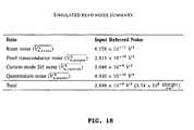
- FIG. 18is a table illustrating a summary for the simulated read noise sources in accordance with an embodiment of the invention.
- FIG. 19is a table illustrating the sensor chip's specification and a summary of the measured performance of the chip in accordance with an embodiment of the invention.
- an active complementary metal oxide semiconductor (CMOS) biosensor chipfor fluorescent-based detection.
- the present inventionprovides several advantages.
- the chipenables time-gated, time-resolved fluorescence spectroscopy.
- a time-gated operationprovides additional background rejection and eases requirements on optical filters.
- the chipalso provides for probe molecules to be immobilized directly on the surface of the chip, thereby eliminating losses associated with the use of large and complex optical filters and also allows for efficient solid-angle collection.
- the ability to distinguish a fluorophore lifetimeadvantageously offers the potential to detect the presence of more than one fluorophore without the need for multiple optical filters.
- Photodiodeswhich are the photosensitive devices compatible with a CMOS process, do not have gain, but use averaging (e.g., in the form of integrating photocurrent onto a capacitor and averaging the results of multiple measurements) in order to achieve a high signal-to-noise ratio (SNR).
- SNRsignal-to-noise ratio
- High sensitivitycan be achieved using a real-time detection application to extract a transient fluorescent decay response that follows the rapid turn-off of an excitation source (e.g., laser).
- Time-gatingimproves the signal-to-background ratio (SBR) of the detector by ensuring that the excitation source is turned off before collecting the photodiode response.
- Sub-samplingis used to achieve this real-time detection.
- the transient responseis repeated a number of times. During each time, the integral of the photodiode current i det (t) is taken from a different starting time (t r ) relative to the laser turn-off time, generating output
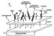
- FIG. 1is a block diagram of a sensor chip 100 in accordance with an embodiment of the invention.
- Chip 100includes a solid support such as a biopolymer layer 102 with probe molecules 104 and 106 (e.g., proteins and nucleic acids) immobilized on the solid support.
- Probes 104 and 106are used to bind to different analytes in a mixture. For example, analytes 108 bind to probes 104 and not to probes 106 .
- Chip 100also includes sensor electronics 110 that detect and process signals generated by analytes 108 .
- chip 100is described herein primarily in the context of using a biopolymer layer 102 as a solid support and having two different probes 104 and 106 immobilized on the solid support for clarity, chip 100 may include any other suitable type of solid support and may have any suitable number of different types of probes for binding to different analytes.
- Analytesmay be labeled with fluorophore molecules.
- the fluorophoresare originally in a ground state.
- an excitation source(not shown) directs a light on chip 100 .
- the excitation sourcecan be any suitable pulsed excitation light source such as, for example, a pulse laser source.
- the pulse laser sourcecan be any suitable laser source such as, for example, a gain switched or a mode-locked laser source.
- the fluorophoresabsorb the light, thereby increasing its energy levels until the fluorophores reach a high-energy excited state. Because the fluorophores are unstable in the high-energy excited state, during an excited lifetime process, the fluorophores lose some of its energy and adopt a lower energy excited state to become semi-stable. During an emission process, the fluorophores releases its excess energy by emitting light until the fluorophores return to the ground state.
- FIG. 2is a timing diagram 200 of time-resolved, time-gated fluorescence detection illustrating a first time period 202 when an excitation source such as a laser is turned on and a second time period 204 when the laser is turned off.
- the laseremits a light, causing fluorophores in analytes 108 to absorb the light and to reach an excited state.
- the fluorescence intensity of the fluorophoresis high.
- the laseris turned off.
- time period 204the intensity of the fluorophores decays at a substantially exponential rate until the ground state is reached.
- sub-sampling of the fluorescence intensity(which can be a measure of the photodiode current) from different starting times t r relative to time 206 , can be measured. These measurements can be averaged to generate a value representing the area under the fluorescent decay response curve (i.e., the integral of the photodiode current).
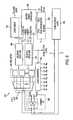
- FIG. 3is a die photograph of a sensor chip 300 in accordance with one embodiment of the invention.
- Chip 300can be a 5 mm ⁇ 5 mm CMOS biosensor chip fabricated in a mixed-signal 0.25 ⁇ m process.
- Chip 300includes an 8 ⁇ 4 pixel array that is divided into four banks (e.g., each bank is arranged as a 4 ⁇ 2 array 302 ) of eight pixels (each having a photodiode) 304 , four current sample-and-hold (SH) circuits 306 , four current-mode ⁇ analog-to-digital converters (ADCs) 308 , reset delay circuitry 310 , ⁇ clocks delay circuitry 312 , laser drivers 314 , a digital controller 316 , and a static random access memory (SRAM) 318 .
- SHcurrent sample-and-hold
- ADCsanalog-to-digital converters
- Laser drivers 314control the operation of an excitation source such as a laser.
- reset delay circuitry 310receives and delays a reset signal (and its complement signal) by a time t r , which is measured relative to the timing of laser drivers 314 .
- the delayed reset signalis sent to pixels 304 in arrays 302 (e.g., to pixel reset predrivers). Pixels 304 receive fluorescent light from the fluorophores, and, upon receiving the delayed reset signal, send as output currents reflecting the fluorescence intensity of the fluorophores.
- the output currentsare time-multiplexed into four SH circuits 306 , which sample the currents and hold the currents for a period of time.
- the sampled current from each SH circuit 306is sent as input to a respective ⁇ ADC 308 , which converts the sampled current from an analog format to a digital format.
- ⁇ ADC 308is controlled by ⁇ clocks delay circuitry 312 .
- Digital resultsare stored in an on-chip memory such as SRAM 318 .
- Digital controller 316which can be configured externally with a serial bit stream, generates the clocks and control signals for ⁇ ADCs 308 , steps through the appropriate t r values, controls the storage of digital samples, and determines the laser pulse duration.
- FIG. 3is described herein as being a particular dimension fabricated on a particular process, with certain configurations of circuitry, any other suitable sizes, processes, and configurations of circuitry may be used.
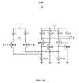
- FIG. 4is a schematic diagram 400 of each pixel 304 .
- Circuit 400includes two reset transistors M 1 and M 2 , an isolation device M 3 , a storage capacitor M 4 , a transconductor 410 , and a diode D 1 420 .
- Diode 420can be an n-well/p-substrate photodiode.
- the photodiode in pixel 304preferably includes an n-well guard ring to collect carriers generated by neighboring pixels 304 .
- Transconductor 410includes multiple transistors M 5 A, M 5 B, M 6 A, M 6 B, and M 7 , and two resistors R 1 A and R 1 B.
- Resistors R 1 A and R 1 Bcan be non-silicided polysilicon resistors that are used to linearize transconductor 410 through source degeneration.
- Transconductor 410converts the voltage across storage capacity M 4 , which results from the integrated photocurrent, into a differential current (I out ) for subsequent current-mode data conversion.
- the transistors in diagram 400may be any suitable type of transistor having any suitable size.
- transistors M 5 A, M 5 B, and/or M 7can be large input n-field-effect transistors (n-FETs) (e.g., 4.32 mm/1 ⁇ m) to reduce 1/f noise and to improve matching performance.
- n-FETsn-field-effect transistors
- C pixelthe capacitance on node V diode (C pixel ), which is the sum of the reverse-biased capacitance of D 1 (C diode ) and the capacitances of M 1 and M 3 (C M1, M3 ).
- C diodecan be about 0.9 ⁇ F while C M1, M3 can be about 10 ⁇ F.
- Transistor M 1is in an ON state, and is sized to provide a triode region resistance of R reset that allows V diode to be held within a particular voltage of V reset , even for large photodiode currents associated with the excitation source.
- the 0.5 ⁇ m M 1 reset deviceis 3 mm to provide a triode region resistance of R reset of about 1.8 ⁇ , which allows V diode to be held within 20 mV of V reset even for photodiode currents as large as 10 mA, which is the photocurrent associated with a 500 W/m 2 635-nm laser.
- Isolation transistor M 3is sized such that it mitigates some of the voltage offset associated with charge-injection from transistor M 1 .
- M 3is 0.5 ⁇ m long and 1.5 mm wide.
- FIG. 5shows an equivalent circuit of the front-end of pixel diagram 400 (diode 420 ) during the reset phase.
- R diodeis the parasitic resistance associated with the n-well bulk connection to diode 420 .
- R diodecan be about 1 k ⁇ , though the resistance may be reduced down to about 200 ⁇ through more careful design.
- the value of R diodelimits the maximum sustainable photocurrent (e.g., to about 1 mA) before blooming can occur in diode 420 (i.e., the diode becomes forward biased because of the voltage drop across R diode ).
- ⁇ diodecan be about 900 ⁇ s and ⁇ M1,M3 can be about 20 ⁇ s.
- the bandwidth critical response of the pixel determined by these time constantsis how quickly the internal diode voltage across C diode (V int ) can track the external diode voltage V diode during the reset phase.
- the laser diode pulse fall-timeis preferably greater than both time constants for the pixel to track the photocurrent up to t r .
- Transistor M 3acts to provide a larger capacitance for charge integration (e.g., 50 ⁇ F when reset is low) while removing the bulk of the capacitance (that of transistor M 4 ) from the performance-limiting time constants.
- i det ⁇ ( t )⁇ - ⁇ ⁇ ⁇ h det ⁇ ( t - t ′ ) ⁇ i em ⁇ ( t ′ ) ⁇ d t ′ ( 1 )
- fluorophore lifetimesare preferably greater than the time constants associated with h det (t).
- i em (t)can be set equal to Q o ⁇ (t).
- the pixel dynamicscan be represented by the following system of differential equations:
- Equation (3)shows that the pixel response time limits the ability of V diode to track v int .
- v diode ⁇ ( t )V reset + Q o C diode + C M ⁇ ⁇ 1 , M ⁇ ⁇ 3 ⁇ e - t r C diode ⁇ R diode - Q o C diode + C M ⁇ ⁇ 1 , M ⁇ ⁇ 3 ⁇ e t r C M ⁇ ⁇ 1 , M ⁇ ⁇ 3 ⁇ R diode ⁇ e - t ⁇ ( C M ⁇ ⁇ 1 , M ⁇ ⁇ 3 + C diode C M ⁇ ⁇ 1 , M ⁇ ⁇ 3 ⁇ C diode ⁇ R diode ) ( 4 )
- Equation (5)represents the total integrated voltage subsequently sensed by the pixel transconductor.
- the actual impulse response h det (t)is proportional to the derivative of ⁇ tilde over (v) ⁇ diode (t r ) with respect to t r :
- the pixel transconductorconverts V diode to a differential current for subsequent current-mode data conversion.
- the transconductanceis approximately:
- g m5is the transconductance of transistor M 5 .
- the simulated 3 dB bandwidthis approximately 2.6 MHz.
- Large input nFETse.g., 4.32 mm/1 ⁇ m
- transistors M 5 A and M 5 Bcan be used to reduce 1/f noise and to improve matching performance. This, along with the large reset devices, limits the fill factor to approximately 13%.
- the overall gain of the pixelis 7.04 ⁇ 10 ⁇ 7 ⁇ A per integrated electron from the photodiode.
- FIG. 6is a simplified top-level schematic diagram 600 of a sensor chip.
- Circuit 600includes the components similar to those illustrated in chip 300 ( FIG. 3 ).
- Circuit 600includes an array 602 having a number of pixels.
- array 602can be array 302 having eight pixels.
- Array 602sends as output differential signal currents for each of the pixels, which are time-multiplexed using multiplexer 604 onto a current-mode SH element 606 .
- current-mode SH element 606can be current SH circuit 306 .
- Current-mode SH element 606can include a differential transconductor with two feedback storage capacitors. The current-mode SH element 606 samples g m,pixel ⁇ tilde over (v) ⁇ diode (t) for one of the multiplexed pixels.
- the output of current-mode SH element 606is continuously sampled by current-mode ⁇ ADC 608 .
- current-mode ⁇ ADC 608can be ⁇ ADC 308 .
- Using a sampled version of the pixel current rather than sending the pixel current directly into ⁇ ADC 608advantageously reduces charge-injection and clock feed-through noise coupling back into array 602 through multiplexer 604 .
- FIG. 7shows a schematic diagram of ⁇ ADC 608 .
- ⁇ ADC 608can be a fully-differential, second-order, one-bit current-output circuit with a full-scale input level.
- the ADCcan deliver a gain of 205 DN per ⁇ A of pixel current.
- clock generator 620can be ⁇ clocks delay circuitry 312 .
- the transconductors in both current-mode SH element 606 and ⁇ ADC 608can use source-degenerating polysilicon resistors, which have a nominal transconductance.
- FIG. 12illustrates a simplified schematic of a transconductor 1200 used in both elements 606 and 608 .
- Transconductor 1200includes a degeneration resistor R 1 for linearization and devices M 3 A and M 3 B as an active cascode.
- transconductoralso includes triode region common-mode feedback devices for properly setting the common-mode level when the transconductor is used with fully differential feedback.
- the closed-loop bandwidthcan be given by
- C hold( ⁇ 58 ⁇ F) is the holding capacitance, implemented as inversion-mode MOS capacitors.
- the bandwidthallows over 12 bits of settling accuracy to be achieved with four-phase nonoverlapping clocks operating with an 8 ⁇ s period.
- the active cascode devices in the output stage of the transconductorcan increase the performance of the circuit by mitigating the effects of finite device output conductance.
- the differential pairsees a very low input impedance (R i ) looking into the active cascode comprised of transistors M 2 and M 3 :
- R ir o ⁇ ⁇ 2 + R L / 2 1 + g m ⁇ ⁇ 2 ⁇ r o ⁇ ⁇ 2 + g m ⁇ ⁇ 2 ⁇ g m ⁇ ⁇ 3 ⁇ r o ⁇ ⁇ 2 ⁇ r o ⁇ ⁇ 3 ( 8 )
- This expressionassumes a differential load resistance of R L loading the transconductor output and that the PMOS current sources have a high output resistance compared to the differential load.
- This low input resistance looking into the active cascodeallows the majority of the current switched by the differential input pair to flow to the output instead of being shunted by the output conductance of the current source “I 1 +I 2 .”
- ⁇ ADC 608generates a one-bit “up” or “down” output that is sent as input to a 24-bit accumulator 610 .
- accumulator 610can be a low-pass digital filter.
- the 12-bit (or other suitable number of bits) value generated by accumulator 610 after running ⁇ ADC 608 for a number of cycles (e.g., 4096 cycles)has a relative accuracy of approximately 11 bits, limited by idle tones in ⁇ ADC 608 .
- the measured detrimental effect of idle tonesis less than what behavioral modeling of ⁇ ADC 608 predicts because of the dithering effect of noise at the input of the ⁇ ADC 608 from current-mode SH element 606 and other analog noise signals in the ⁇ ADC 608 loop.
- Results from accumulator 610are cached into an on-chip memory (e.g., SRAM 318 ). This eliminates the need for firing noisy off-chip drivers during repeated measurements.
- the outputs of the four accumulators 610(each associated with a different array 302 ), are sent as input to a memory (e.g., SRAM) controller that coordinates writing this data to a single memory array.
- the address space of SRAM 318is organized by sub-blocks and by which pixel within the sub-block is being written.
- SRAM 318can be written in a single-pixel mode (e.g., a maximum of 2048 24-bit pixels values) or in a multiple-pixel mode (e.g., 64 values for each of 32 pixels). When measurements are completed and stored in SRAM 318 , the entire contents of SRAM 318 can then be loaded off-chip.
- thiscan be performed in less than 310 ⁇ s.
- a single measurementcan take 4097 ADC cycles to complete with one additional cycle used to allow SH element 606 to settle.
- one measurement on each of the four pixelscan be repeated every 33 ms.
- Other suitable numbers of cycles and time periodscan also be used in performing these measurements.
- Circuit 600also includes master digital controller 612 , which drives both the array reset signal and the excitation source (e.g., a laser).
- master digital controller 612can be digital controller 316 . Controller 612 can vary the skew between the signals of the reset signal and the laser to achieve time-resolved fluorescence detection.
- Laser driver 614can include a variable width inverter with independent tunability of the pull-up and pull-down widths, selected digitally using control words (e.g., two seven-bit words).
- laser driver 614can be laser driver 314 . Laser diodes with larger operating voltages can be accommodated by using thick oxide input/output (I/O) in the output circuitry of the laser driver.
- I/Othick oxide input/output
- a thick oxide 3.3 V I/Ocan be used. This also allows the laser diode to tolerate overshoot at the near-end, which sometimes occurs as a result of reflections against the highly nonlinear load resistance turn-on characteristic of the laser diode.
- the maximum current sourcing capabilitycan be at any suitable voltage output that is sufficient to drive commercial laser diodes with certain optical outputs. Larger laser diodes can be sized such that they can be suitably driven by off-chip transmission lines in parallel. Pulse width and synchronization can be determined by controller 612 .
- the maximum current sourcing capability at 2.7 V outputcan be greater than 130 mA, which is sufficient to drive commercial laser diodes with 50 mW of optical output.
- Large laser diodes with input capacitances of up to 40 ⁇ Fcan be driven by up to four off-chip 50- ⁇ transmission lines in parallel, resulting in near-end fall times of about 500 ⁇ s.
- the pulse widthcan be varied in 50 ns intervals up to 204.8 ⁇ s, but typically a pulse width of 300 ns is used.
- Circuit 600further includes programmable, variable delay lines 616 and 618 used to trigger the pixel reset predrivers in array 602 .
- Delay line 616delays the reset signal while delay line 618 delays the complement of the reset signal.
- An n-bit multiplexercan be used to choose one of the phases in each delay line 616 and 618 .
- the phases in each delay line 616 and 618are preferably the complement of the other.
- Each delay line 616 and 618 and multiplexeris designed to limit mismatch between buffer stages that results from layout parasitics.
- Large on-chip drivers for the reset and laser diode driversare designed to rapidly switch to achieve sufficient resolution for time-resolved detection. This can result in power-supply and substrate noise issues that may be a concern for the sensitive analog circuits of array 602 and ⁇ ADC 608 .
- Several techniquescan be implemented to minimize these issues. For example, the slew rate of the reset signal can be limited to control noise generation.
- Array 602 and ⁇ ADC 608can be isolated from one another and other circuitry using a double guard ring. Supplies can be separated and decoupled on the chip. Data inputs to, and data outputs from, the chip can also be separated (e.g., all bias currents and voltages can sent as input into one side of the chip while all digital signals can be interfaced from another side of the chip).
- Circuit read noise and photon shot noisedetermine the SNR and the dynamic range for the measurement of ⁇ tilde over (v) ⁇ diode (t).
- the read noisegenerally include four major components: the pixel reset noise, the pixel transconductor noise, the current-mode SH noise, and the quantization noise of the ADC. Averaging of repeated measurements can be used to reduce the first three read noise sources, thereby leaving the system noise floor determined by the quantization limit of the ADC. Simulated read noise sources are summarized in the table in FIG. 18 .
- C pixelC diode +C M1,M3 and the sampling capacitance C M4 , which is determined by the gate capacitance of M 4 .
- C pixelcan be approximately 10.9 ⁇ F
- C M4can be approximately 30 ⁇ F.
- Long reset timesare typically used to provide a steady-state system.
- the sampled noise voltage power on a capacitor Ccan be given by kT/C.
- the total mean-squared noise chargecan be given by the following expression:
- Pixel transconductance noiseReferring to FIG. 4 , the pixel transconductance noise is dominated by the thermal noise of the degeneration resistor and the channel thermal noise of transistors M 5 and M 6 .
- the drain current noise power spectral density (PSD) of transistor M 5can be given by the following expression:
- FIG. 13shows a partial circuit 1300 used for this analysis.
- the noise voltageis stored at node V x .
- R iis the output resistance of the driving stage (pixel transconductor), modeled by the current source I i .
- Resistors R m and R sare the respective analog multiplexor switch on-resistance and current-mode SH feedback switch on-resistance.
- the transconductoris modeled as an ideal transconductor with transconductance g m and output resistance r o .
- the sampled noise voltage on V xis dominated by the noise of R s and the transconductor equivalent output noise current.
- r o>>R s
- g m r othe total integrated noise sampled on V x from the switch resistance R s can be given by the following expression:
- V n,currsh 2The total sampled noise on V x , given by V n,gm 2 + V n,Rs 2 , when input-referred to v diode is denoted as V n,currsh 2 in the table in FIG. 18 .
- This noise(e.g., 2.046 ⁇ 10 ⁇ 9 V 2 ) can constitute more than two-thirds of the total read noise of the sensor.
- the equivalent quantization noise ( V n,quant 2 ) referred back to the pixel v diode nodeis 4.930 ⁇ 10 ⁇ 10 V 2 , assuming a 12-bit data conversion and a 30-mV swing on ⁇ tilde over (v) ⁇ diode (t).
- the total mean squared noiseis 54 ⁇ V, which corresponds to approximately 3.74 ⁇ 10 8 photons/cm 2 for a quantum efficiency of 45% and capacitance C pixtotal of approximately 50 ⁇ F.
- the mean-square shot noise chargecan be given by the following expression:
- V n , sh 2 _Q n , sh 2 _ C pixtotal 2 .
- the time-gated behavior of the sensorprovides for background rejection of the excitation source, even in the absence of optical filtering.
- the background excitation reaching the sensoris assumed to have an exponential decay time given by ⁇ diode , which is valid if ⁇ diode is much larger than the laser turn-off time.
- fluorophores excited during the turn-off transientcan be ignored so that the fluorescent signal is characterized by a decay time given by the fluorescent lifetime ⁇ fluor , which is valid if ⁇ fluor >> ⁇ diode .
- Q totalcan represent the total charge generated in the sensor due to the pulsed excitation source in the absence of fluorophores.
- I background ⁇ ( t )( 1 - ⁇ ⁇ ⁇ c surface ) ⁇ Q total ⁇ diode ⁇ e - t / ⁇ diode ( 19 )
- I signal ⁇ ( t )⁇ ⁇ ⁇ ⁇ ⁇ ⁇ c surface ⁇ fluor ⁇ e - t / ⁇ fluor ( 20 ) where ⁇ is the quantum yield of the dye.
- SBRsignal-to-background ratio
- SBR dBt r ⁇ 20 ln ⁇ ( 10 ) ⁇ ⁇ diode - ⁇ ⁇ diode ⁇ ⁇ ⁇ ⁇ diode ⁇ ⁇ + 20 ⁇ ⁇ log 10 ( ⁇ ⁇ ⁇ c surface ⁇ ⁇ 1 - ⁇ ⁇ ⁇ c surface ) ( 22 )
- SBR dBincreases linearly with t r , while the SNR decreases with increasing t r .
- an optimal value of t r for detectionoccurs when the SNR equals the SBR.
- FIG. 14shows the measured external quantum efficiency of the n-well/p-substrate photodiode as a function of the wavelength using a standard measurement set-up including a monochromator, integrating sphere, and calibrated photodetector.
- peak quantum efficiencies in the range of 0.45-0.5 electrons/photonsoccur at wavelengths between 600-700 nm for the relatively deep diode junctions, suggesting a peak performance for dyes operating in this wavelength range.
- the dye AlexaFluor 633has a peak absorption at around 630 nm.
- the structure in the curve, particularly evident for the longer wavelengths,is due to interference effects in the dielectric stack.
- FIG. 8is a block diagram of is a block diagram of fluorescent-based detection system 800 in accordance with an embodiment of the invention.
- System 800includes a first printed circuit board (PCB) 802 .
- a biochip sensorwhich can be packaged in a ceramic quad-flat-pack (QFP) package 804 , is mounted on PCB 802 .
- the biochip sensorcan include the circuitry shown in FIGS. 3-7 .
- System 800also includes a second PCB 806 .
- Laser circuitry 808which includes a laser diode, a lens holder, a collimating lens, and a focusing lens, is mounted on PCB 806 .
- the laser diodecan be a 635 nm, 5 mW AlGaInP diode packaged in a 9 mm CAN style package. Alternatively, any other suitable diode can be used.
- PCB 806is mounted over PCB 802 such that circuitry 808 can direct the light over analytes bound to the probes on the surface of biochip 804 .
- Cables 810 with connectors 812e.g., SubMiniature version A or SMA connectors
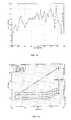
- FIG. 15characterizes the sensitivity of the sensor.
- t ris chosen to position the end of the reset phase 8.5 ns before the laser diode turn-off, allowing the laser diode power to be directly integrated in the sensor.
- Neutral density filterscan be used to vary the laser signal strength. While the natural density filters have transmission tolerances of about ⁇ 10%, the transmission of individual neutral density filters can be calibrated to remove this source of possible measurement error. As shown in FIG. 15 , each point in the signal curve is the average of 2047 measurements.
- the noise curves of FIG. 15can be generated by taking the average of blocks of N consecutive measurements in the original 2047 measurement dataset.
- the standard deviation of the floor (2047/N) averaged blocks of datais recorded as the-noise after averaging.
- the noise curvesshow the effect of averaging on reducing the noise floor of the system.
- the noise curvesshow the effect of averaging on reducing the noise floor of the system.
- Averaging 64 pointsyields a noise floor close to the 12-bit quantization noise limit of the system.
- the noise curvesacquire a one-half slope due to photon shot noise.
- the systemshows a peak SNR, limited by photon shot noise, of 64 dB and dynamic range of 74 dB.
- the read noise floor of the sensor (without averaging) shown in FIG. 15(e.g., 5 ⁇ 10 8 photons/cm 2 ) is slightly larger than that predicted by simulation (e.g., 3.74 ⁇ 10 8 photons/cm 2 ). This may be due to a slight underestimation of the read noise contribution of the pixel transconductor.
- the measured dark current in the photodiodeis approximately 2.31 ⁇ A, which corresponds to a dark current signal from the pixel transconductor of 10.4 ⁇ A per second of integration.
- the corresponding dark current shot noise levelis approximately 10 ⁇ 3 digital numbers (DN) for 12-bit conversion, well below the quantization noise limit.
- the dynamic rangeis the true dynamic range of the sensor.
- the excitation sourcelaser diode
- the effective dynamic rangecan be reduced because the sensor will saturate at lower fluorescent signal levels.
- FIG. 16illustrates an illustrative embodiment of the time-domain response of the sensor in which t r is varied to reconstruct the actual turn-off transient of the laser.
- the solid linerepresents the output from a 12 GHz-bandwidth, New Focus 1577-A photodetector as measured by an Agilent 86100B oscilloscope.
- the circlesshow the numerically differentiated output of the sensor.
- the laser fall-timeis varied from approximately 1 ns to 5 ns. For the fastest -fall times, the sensor output can lag the high-speed detector output due to the limitations of the ⁇ diode time constant described above.
- the impulse response of the systemis measured, for example, using a PiLas Picosecond Laser Diode System with a 635 nm laser diode head.
- the laseris capable of producing laser pulses of less than 40 ⁇ s FWHM with peak collimated beam power as high as 150 mW.
- the laseris triggered by the chip's laser driver output.
- the delay from the chip's laser driver signal to when the laser is actually firedcan be controlled by varying the coaxial cable length carrying the trigger signal.
- FIG. 17shows the numerically differentiated ADC output of the system for an impulse excitation.
- each time sampleis measured 32 times and subsequently averaged to get the final waveform.
- the circuitsdepict the numerically differentiated output of the sensor.
- the systemshows an exponential decay. An artifact of the 4-point numerical differentiation algorithm is apparent during the beginning of the pulse because the algorithm does not produce accurate results for a signal with such a high frequency edge and effectively low-pass filters it.
- the exponential decayhas a time constant ( ⁇ diode ) of 1.2 ns, suggesting a parasitic R diode resistance of approximately 1400 ⁇ .
- ⁇ diodeEven for long-lifetime quantum-dot fluorophores, time-gating alone generally does not provide adequate background rejection for detection. To detect surface concentrations on the order of 10 8 cm ⁇ 2 , at least 160 dB of excitation rejection is needed. Even if ⁇ diode were reduced through design improvement to 500 ⁇ s, time-gating alone would not provide sufficient SBR. As a result, a thin-film optical filter can be added to the chip to provide sufficient SBR. For example, in one embodiment, an OD 5 23-layer SiO 2 /T i O 2 thin-film optical filter can be added to the chip. This filter, combined with time-gating, can thus result in more than 160 dB of background rejection being achieved.
- FIG. 9is a flow chart illustrating different states of a fluorophore during fluorescent-based detection.
- Process 900begins at step 902 where a fluorophore is in a ground state.
- an excitation sourcesuch as a laser is turned on
- process 900moves to an excitation process at step 904 .
- a fluorophoreabsorbs light, increasing its energy level until it reaches a high energy excited state.
- Process 900then moves to an excited lifetime process at step 906 .
- the fluorophoreloses some of its energy to adopt a lower energy excited state.
- the laseris turned off, process 900 moves to an emission process 908 .
- the fluorophoresreleases its excess energy by emitting light until the fluorophore returns to the ground state at step 910 .
- FIG. 10is flow chart illustrating a process 1000 for fluorescent-based detection in accordance with one embodiment of the invention.
- Process 1000begins at step 1002 where an excitation source such as a laser is turned on.
- process 1000determines whether the laser should be turned off.
- the lasermay be programmed to be turned off after a predetermined time period, based on particular conditions (e.g., based on measurements in the array), or based on any other suitable measurement.
- process 1000remains at step 1004 .
- process 1000moves to step 1006 where the laser is turned off.
- the operation of the lasermay be controlled by any suitable circuitry such as, for example, controllers 316 and 612 and/or laser drivers 314 or 614 .
- process 1000determines whether the time that has elapsed, which is measured from the time that the laser is turned off, equals a particular rest time (t reset ).
- the reset timemay be any suitable time and may be controlled by any suitable circuitry such as, for example, controllers 316 and 612 and/or delay lines 310 , 616 , and 618 .
- process 1000remains at step 1008 .
- process 1000moves to step 1010 where the photodiode current (in a pixel 304 ) is measured.
- process 1000determines whether the measurements are completed.
- process 1000moves to step 1014 where the reset time is changed (e.g., t reset is incremented by a particular amount ⁇ ).
- any suitable number of measurementsmay be taken using any suitable number of reset times (t reset ) such that the measurements can be used to uniquely identify the transient fluorescent decay response of a given fluorophore from other fluorophores.
- the reset timemay change by the same predetermined incremental value.
- the rest timemay change using different incremental values (e.g., as the elapsed time from the time that the laser is turned off increases, the incremental value may also increase).
- the same reset timemay be used for subsequent measurements to improve the overall detection sensitivity.
- the reset timemay be set and/or changed by any suitable circuitry such as, for example, controllers 316 and 612 and/or delay lines 616 and 618 .
- step 1012process 1000 moves to step 1016 where the measurements are averaged to generate a representation of the transient fluorescent decay response of a particular fluorophore.
- These measurementscan then be stored in an on-chip memory such as SRAM 306 or used for further processing of the data.
- Steps 1010 , 1012 , and 1016may be performed using any suitable circuitry such as, for example, current SH elements 306 or 606 , ⁇ ADCs 308 or 608 , and/or accumulator 610 .
- FIG. 11is flow chart illustrating a process 1100 for fluorescent-based detection in accordance with another embodiment of the invention.
- Process 1100begins at step 1102 where an excitation source such as a laser is turned on.
- process 1100determines whether the laser should be turned off.
- the lasermay be programmed to be turned off after a predetermined time period, based on particular conditions (e.g., based on measurements in the array), or based on any other suitable measurement.
- process 1100remains at step 1104 .
- process 1100moves to step 1106 where the laser is turned off.
- the operation of the lasermay be controlled by any suitable circuitry such as, for example, controllers 316 and 612 and/or laser drivers 314 and 614 .
- a reset signalmay be delayed prior to being sent to array 302 or 602 .
- the reset signal(and its complement signal) may be sent from controller 612 to delay line 616 (and 618 ) when the laser is turned off.
- Delay line 616may delay the reset signal by a reset time (t reset ) (as described above in connection with FIG. 10 ).
- t resetreset time
- process 1100moves to step 1110 where the process drives pixel reset predrivers in array 302 or 602 with the delayed reset signal, causing the pixels in array 302 or 602 to output pixel signal currents.
- process 1100time multiplexes the pixel signal currents. This may be performed using multiplexer 604 .
- the time-multiplexed pixel signal currentsare sampled and held for a period of time. This may be performed using current SH circuits 306 or 606 . After the period of time, the sampled currents are converted from analog to digital format at step 1116 . This may be performed using ⁇ ADCs 308 or 608 .
- process 1100accumulates the converted data. This may be performed using accumulator 610 . Although steps 1116 and 1118 are shown as separate sequential steps, ⁇ ADCs 308 or 608 perform many cycles of converting sampled currents to digital format and sending the output to accumulator 610 . Once all the data is accumulated, process 1100 moves to step 1120 where the accumulated results are stored. The results may be stored in an on-chip memory such as SPAM 306 .
- Process 1100illustrates a process for fluorescent-based detection measured at one rest time (t reset ). Although not shown, process 1100 may be repeated a number of times. In one embodiment, the reset time in which fluorescent-based detection is measured may change with each subsequent measurement. In another embodiment, the reset time in which the fluorescent-based detection is measured may be the same with each subsequent measurement.
- CMOS biosensor chipfor fluorescent-based assays that enables time-gated, time-resolved fluorescence spectroscopy.
- the biosensor chipprovides capabilities beyond those of macroscopic instrumentation by enabling time-gated operation for background rejection, easing requirements on optical filters, and by characterizing fluorescence lifetime, allowing for a more detailed characterization of fluorophore labels and their environment.
- the biosensor chipcan be used for a variety of applications including biological, medical, and in-the-field applications.
- the biosensor chipcan be used for DNA and protein microarrays where the biomolecular probe is attached directly to the chip surface.
- the biosensor chipcan also be used as a general fluorescent lifetime imager in a wide-field or confocal microscopy system.
- the biosensor chipcan be used as an imager in a conventional widefield epifluorescent microscope for lifetime imaging.
Landscapes
- Health & Medical Sciences (AREA)
- Physics & Mathematics (AREA)
- Immunology (AREA)
- Chemical & Material Sciences (AREA)
- Nuclear Medicine, Radiotherapy & Molecular Imaging (AREA)
- Engineering & Computer Science (AREA)
- Life Sciences & Earth Sciences (AREA)
- Signal Processing (AREA)
- Analytical Chemistry (AREA)
- Biochemistry (AREA)
- General Health & Medical Sciences (AREA)
- General Physics & Mathematics (AREA)
- Multimedia (AREA)
- Pathology (AREA)
- Chemical Kinetics & Catalysis (AREA)
- Optics & Photonics (AREA)
- Investigating, Analyzing Materials By Fluorescence Or Luminescence (AREA)
Abstract
Description
- Sub-sampling preserves the sensitivity benefits of averaging (by integrating the photocurrent response) and reduces the bandwidth requirements on circuit components because the interval between repeated measurements can be used for data conversion, potentially overlapping with the integration of the next measurement. The result for a single starting time (tr) can also be repeated to improve the overall detection sensitivity. The photodiode current idet(t), which is directly proportional to the instantaneous fluorescence, can be generated by numerical differentiation.
The pixel time constants and the fluorophore lifetime are reflected in idet(t). To be easily determinable, fluorophore lifetimes are preferably greater than the time constants associated with hdet(t). To calculate an expression for hdet(t) for the pixel, iem(t) can be set equal to Qoδ(t). The pixel dynamics can be represented by the following system of differential equations:
with Vdiode(t)=Vreset. Equation (3) shows that the pixel response time limits the ability of Vdiodeto track vint. Using these expressions to determine vint(tr) and Vdiode(tr) and using these as initial conditions for the solution of
Equation (5) represents the total integrated voltage subsequently sensed by the pixel transconductor. The actual impulse response hdet(t) is proportional to the derivative of {tilde over (v)}diode(tr) with respect to tr:
where gm5is the transconductance of transistor M5. In an illustrative embodiment, R1A=R1B=500Ω, yielding a measured transconductance of about 0.22 mS. The simulated 3 dB bandwidth is approximately 2.6 MHz. Large input nFETs (e.g., 4.32 mm/1 μm), transistors M5A and M5B, can be used to reduce 1/f noise and to improve matching performance. This, along with the large reset devices, limits the fill factor to approximately 13%. The overall gain of the pixel is 7.04×10⁻⁷μA per integrated electron from the photodiode.
where Chold(≅58 ρF) is the holding capacitance, implemented as inversion-mode MOS capacitors. In this example, the bandwidth allows over 12 bits of settling accuracy to be achieved with four-phase nonoverlapping clocks operating with an 8 μs period.
This expression assumes a differential load resistance of RLloading the transconductor output and that the PMOS current sources have a high output resistance compared to the differential load. This low input resistance looking into the active cascode allows the majority of the current switched by the differential input pair to flow to the output instead of being shunted by the output conductance of the current source “I1+I2.” The active cascode can also boost the output impedance (Ro) of the transconductor:
Ro=[ro2+req+gm2ro2req+gm2gm3ro2ro3req]∥roI2 (9)
where reqis the parallel combination of the NMOS current source and impedance looking into the differential pair device M1 and roI2is the output resistance of current source I2. In this case, the larger the output impedance of the transconductor, the less significant the loading effects of the next stage become.
After reset, the switch M3 is turned on while switches M1 and M2 are turned off. The effective capacitance of the input node to the pixel transconductor can be given by Cpixtotal=Cpixel+CM4(e.g., ≈50 ρF with the additional capacitance of the switch M3). Consequently, the mean-squared noise voltage at the input to the transconductor due to the reset devices can be given by the following expression:
KM5is the 1/f noise constant for M5 and IDS5is the drain to source current of M5. Transistor M5 is biased in moderate inversion but close enough to weak inversion to justify the use of weak-inversion expressions for noise analysis. Similarly, the drain current noise PSD of transistor M6 can be given by the following expression:
Transistor M6 can be biased near strong inversion so that this strong inversion noise expression can be used. Finally, the resistor current noise PSD of degeneration resistor R1can be given by the following expression:
In this illustrative embodiment, using these expressions in simulation results in a total integrated input reference noise power of 2.915×10⁻¹⁰V2. The 1/f noise sources of the pixel transconductor represent approximately 10% of the total noise over the integrated bandwidth.
This noise decreases as both the transconductance and holding capacitance of the current-mode SH increase. For large ro, the total integrated noise due to the equivalent single-ended transconductor output current noise power spectral density Sn,gmcan be given by the following expression:
Once again, the circuit becomes less noisy when both the transconductance and holding capacitance increase. The total sampled noise on Vx, given by
Assuming that the fluorophore's response is a monoexponential decay represented by iem(t)=Ioe−t/τ
This yields an input-referred mean-square voltage noise of
- Since the signal power is proportional to e−2t
r /τ, the SNR in the shot-noise-limited regime decreases with increasing tras e−tr /τ.
- Since the signal power is proportional to e−2t
where η is the quantum yield of the dye.
Expressing this in units of decibels yields the following expression:
SBRdBincreases linearly with tr, while the SNR decreases with increasing tr. In one embodiment, an optimal value of trfor detection occurs when the SNR equals the SBR.
Claims (26)
Priority Applications (1)
| Application Number | Priority Date | Filing Date | Title |
|---|---|---|---|
| US11/800,468US7738086B2 (en) | 2005-05-09 | 2007-05-04 | Active CMOS biosensor chip for fluorescent-based detection |
Applications Claiming Priority (4)
| Application Number | Priority Date | Filing Date | Title |
|---|---|---|---|
| US67954505P | 2005-05-09 | 2005-05-09 | |
| US79940806P | 2006-05-09 | 2006-05-09 | |
| US11/431,405US20070097364A1 (en) | 2005-05-09 | 2006-05-09 | Active CMOS biosensor chip for fluorescent-based detection |
| US11/800,468US7738086B2 (en) | 2005-05-09 | 2007-05-04 | Active CMOS biosensor chip for fluorescent-based detection |
Related Parent Applications (1)
| Application Number | Title | Priority Date | Filing Date |
|---|---|---|---|
| US11/431,405Continuation-In-PartUS20070097364A1 (en) | 2005-05-09 | 2006-05-09 | Active CMOS biosensor chip for fluorescent-based detection |
Publications (2)
| Publication Number | Publication Date |
|---|---|
| US20080037008A1 US20080037008A1 (en) | 2008-02-14 |
| US7738086B2true US7738086B2 (en) | 2010-06-15 |
Family
ID=39050404
Family Applications (1)
| Application Number | Title | Priority Date | Filing Date |
|---|---|---|---|
| US11/800,468Active2027-06-11US7738086B2 (en) | 2005-05-09 | 2007-05-04 | Active CMOS biosensor chip for fluorescent-based detection |
Country Status (1)
| Country | Link |
|---|---|
| US (1) | US7738086B2 (en) |
Cited By (59)
| Publication number | Priority date | Publication date | Assignee | Title |
|---|---|---|---|---|
| US20090075843A1 (en)* | 2007-09-14 | 2009-03-19 | Iii-N Technology, Inc. | Biological Sensor System |
| WO2013147388A1 (en)* | 2012-03-28 | 2013-10-03 | 광주과학기술원 | High sensitivity biosensor using pixel analysis of cmos image sensor |
| US8906320B1 (en) | 2012-04-16 | 2014-12-09 | Illumina, Inc. | Biosensors for biological or chemical analysis and systems and methods for same |
| US8981318B1 (en)* | 2011-12-30 | 2015-03-17 | Gene Capture, Inc. | Multi-dimensional scanner for nano-second time scale signal detection |
| US9195043B2 (en) | 2010-08-27 | 2015-11-24 | The Board Of Trustees Of The Leland Stanford Junior University | Microscopy imaging device with advanced imaging properties |
| US9513220B1 (en) | 2015-12-29 | 2016-12-06 | International Business Machines Corporation | On-chip molecule fluorescence detection |
| US9606058B2 (en) | 2014-08-08 | 2017-03-28 | Quantum-Si Incorporated | Integrated device for temporal binning of received photons |
| US9617594B2 (en) | 2015-05-20 | 2017-04-11 | Quantum-Si Incorporated | Pulsed laser and bioanalytic system |
| US9678012B2 (en) | 2014-08-08 | 2017-06-13 | Quantum-Si Incorporated | Integrated device with external light source for probing detecting and analyzing molecules |
| US9831283B2 (en) | 2011-10-31 | 2017-11-28 | The Trustees Of Columbia University In The City Of New York | Systems and methods for imaging using single photon avalanche diodes |
| US9863880B2 (en) | 2013-11-17 | 2018-01-09 | Quantum-Si Incorporated | Optical system and assay chip for probing, detecting and analyzing molecules |
| US9921157B2 (en) | 2014-08-08 | 2018-03-20 | Quantum-Si Incorporated | Optical system and assay chip for probing, detecting and analyzing molecules |
| US10174363B2 (en) | 2015-05-20 | 2019-01-08 | Quantum-Si Incorporated | Methods for nucleic acid sequencing |
| US10254225B2 (en) | 2013-12-10 | 2019-04-09 | Illumina, Inc. | Biosensors for biological or chemical analysis and methods of manufacturing the same |
| US10283928B2 (en) | 2016-12-16 | 2019-05-07 | Quantum-Si Incorporated | Compact mode-locked laser module |
| US10580820B2 (en)* | 2018-07-16 | 2020-03-03 | Gigajot Technology Inc. | High-sensitivity depth sensor with non-avalanche photodetector |
| US10605730B2 (en) | 2015-05-20 | 2020-03-31 | Quantum-Si Incorporated | Optical sources for fluorescent lifetime analysis |
| US10656088B2 (en) | 2016-08-12 | 2020-05-19 | Silanna UV Technologies Pte Ltd | Ultraviolet biosensor |
| US10845308B2 (en) | 2016-12-22 | 2020-11-24 | Quantum-Si Incorporated | Integrated photodetector with direct binning pixel |
| US10861829B2 (en) | 2017-12-26 | 2020-12-08 | Illumina, Inc. | Sensor system |
| US10956787B2 (en) | 2018-05-14 | 2021-03-23 | Quantum-Si Incorporated | Systems and methods for unifying statistical models for different data modalities |
| US11001881B2 (en) | 2006-08-24 | 2021-05-11 | California Institute Of Technology | Methods for detecting analytes |
| US11072827B2 (en) | 2018-01-08 | 2021-07-27 | Quantum-Si Incorporated | System and methods for electrokinetic loading of sub-micron-scale reaction chambers |
| US20210277463A1 (en)* | 2015-05-20 | 2021-09-09 | Quantum-Si Invorporated | Pulsed laser and bioanalytic system |
| US11128098B2 (en) | 2018-05-03 | 2021-09-21 | Quantum-Si Incorporated | Characterizing an optical element |
| US11226290B2 (en) | 2016-06-01 | 2022-01-18 | Quantum-Si Incorporated | Photonic structures and integrated device for detecting and analyzing molecules |
| US11237326B2 (en) | 2017-07-24 | 2022-02-01 | Quantum-Si Incorporated | Optical rejection photonic structures using two spatial filters |
| US11249318B2 (en) | 2016-12-16 | 2022-02-15 | Quantum-Si Incorporated | Compact beam shaping and steering assembly |
| US11322413B2 (en) | 2018-08-29 | 2022-05-03 | Quantum-Si Incorporated | Sample well fabrication techniques and structures for integrated sensor devices |
| US11344200B2 (en) | 2016-02-17 | 2022-05-31 | Tesseract Health, Inc. | Sensor and device for lifetime imaging and detection applications |
| US11360029B2 (en) | 2019-03-14 | 2022-06-14 | Insilixa, Inc. | Methods and systems for time-gated fluorescent-based detection |
| US11391626B2 (en) | 2018-06-22 | 2022-07-19 | Quantum-Si Incorporated | Integrated photodetector with charge storage bin of varied detection time |
| US11447816B2 (en) | 2006-07-28 | 2022-09-20 | California Institute Of Technology | Multiplex Q-PCR arrays |
| US11454758B2 (en) | 2019-08-08 | 2022-09-27 | Quantum-Si Incorporated | Optical microdisks for integrated devices |
| US11466316B2 (en)* | 2015-05-20 | 2022-10-11 | Quantum-Si Incorporated | Pulsed laser and bioanalytic system |
| US11485997B2 (en) | 2016-03-07 | 2022-11-01 | Insilixa, Inc. | Nucleic acid sequence identification using solid-phase cyclic single base extension |
| US11525156B2 (en) | 2006-07-28 | 2022-12-13 | California Institute Of Technology | Multiplex Q-PCR arrays |
| US11538556B2 (en) | 2018-01-26 | 2022-12-27 | Quantum-Si Incorporated | Machine learning enabled pulse and base calling for sequencing devices |
| US11560588B2 (en) | 2006-08-24 | 2023-01-24 | California Institute Of Technology | Multiplex Q-PCR arrays |
| US11573180B2 (en) | 2020-04-08 | 2023-02-07 | Quantum-Si Incorporated | Integrated sensor with reduced skew |
| US11692938B2 (en) | 2019-06-19 | 2023-07-04 | Quantum-Si Incorporated | Optical nanostructure rejecter for an integrated device and related methods |
| US11714001B2 (en) | 2020-10-22 | 2023-08-01 | Quantum-Si Incorporated | Integrated circuit with sequentially-coupled charge storage and associated techniques comprising a photodetection region and charge storage regions to induce an intrinsic electric field |
| US11719639B2 (en) | 2020-03-02 | 2023-08-08 | Quantum-Si Incorporated | Integrated sensor for multi-dimensional signal analysis |
| US11747561B2 (en) | 2019-06-14 | 2023-09-05 | Quantum-Si Incorporated | Sliced grating coupler with increased beam alignment sensitivity |
| US11774674B2 (en) | 2019-01-03 | 2023-10-03 | Quantum-Si Incorporated | Optical waveguides and couplers for delivering light to an array of photonic elements |
| US11804499B2 (en) | 2019-06-28 | 2023-10-31 | Quantum-Si Incorporated | Optical and electrical secondary path rejection |
| US11808700B2 (en) | 2018-06-15 | 2023-11-07 | Quantum-Si Incorporated | Data acquisition control for advanced analytic instruments having pulsed optical sources |
| US11869917B2 (en) | 2020-01-14 | 2024-01-09 | Quantum-Si Incorporated | Integrated sensor for lifetime characterization |
| US11885744B2 (en) | 2020-01-14 | 2024-01-30 | Quantum-Si Incorporated | Sensor for lifetime plus spectral characterization |
| US11967436B2 (en) | 2018-05-30 | 2024-04-23 | Quantum-Si Incorporated | Methods and apparatus for making biological predictions using a trained multi-modal statistical model |
| US11971963B2 (en) | 2018-05-30 | 2024-04-30 | Quantum-Si Incorporated | Methods and apparatus for multi-modal prediction using a trained statistical model |
| US12078596B2 (en) | 2017-07-24 | 2024-09-03 | Quantum-Si Incorporated | Hand-held, massively-parallel, bio-optoelectronic instrument |
| US12142619B2 (en) | 2019-10-31 | 2024-11-12 | Quantum-Si Incorporated | Pixel with enhanced drain |
| US12159887B2 (en) | 2022-08-19 | 2024-12-03 | Quantum-Si Incorporated | Backside illuminated structures with parallel charge transfer |
| US12170433B2 (en) | 2020-01-14 | 2024-12-17 | Quantum-Si Incorporated | Amplitude-modulated laser |
| US12179204B2 (en) | 2018-12-03 | 2024-12-31 | Quantum-Si Incorporated | Sample well fabrication techniques and structures for integrated sensor |
| US12188868B2 (en) | 2020-01-14 | 2025-01-07 | Quantum-Si Incorporated | Waveguide excitation uniformity |
| US12297496B2 (en) | 2020-12-11 | 2025-05-13 | Quantum-Si Incorporated | Integrated circuit with improved charge transfer efficiency and associated techniques |
| US12317615B2 (en) | 2021-04-08 | 2025-05-27 | Quantum-Si Incorporated | Integrated circuit having mirrored pixel configuration |
Families Citing this family (28)
| Publication number | Priority date | Publication date | Assignee | Title |
|---|---|---|---|---|
| US11098345B2 (en)* | 2006-06-05 | 2021-08-24 | California Institute Of Technology | Methods for detecting target analytes |
| US8999724B2 (en)* | 2006-12-28 | 2015-04-07 | Intel Corporation | Method and apparatus for match quality analysis of analyte binding |
| US7767441B2 (en) | 2007-10-25 | 2010-08-03 | Industrial Technology Research Institute | Bioassay system including optical detection apparatuses, and method for detecting biomolecules |
| US7811810B2 (en)* | 2007-10-25 | 2010-10-12 | Industrial Technology Research Institute | Bioassay system including optical detection apparatuses, and method for detecting biomolecules |
| US9778188B2 (en) | 2009-03-11 | 2017-10-03 | Industrial Technology Research Institute | Apparatus and method for detection and discrimination molecular object |
| GB0904934D0 (en)* | 2009-03-23 | 2009-05-06 | Geneseqe As | Method and apparatus for detecting molecules |
| WO2010119371A1 (en)* | 2009-04-15 | 2010-10-21 | Koninklijke Philips Electronics N.V. | Device for time controlled fluorescence detection |
| EP2270477B1 (en)* | 2009-07-03 | 2015-09-09 | Nxp B.V. | System and method for detecting luminescence |
| TWI397679B (en)* | 2009-07-30 | 2013-06-01 | Ind Tech Res Inst | Apparatuses and methods for detecting fluorescence |
| EP2933629B1 (en) | 2010-02-19 | 2019-04-10 | Pacific Biosciences Of California, Inc. | System for measuring analytical reactions comprising a socket for an optode array chip |
| US9482615B2 (en) | 2010-03-15 | 2016-11-01 | Industrial Technology Research Institute | Single-molecule detection system and methods |
| US8865078B2 (en) | 2010-06-11 | 2014-10-21 | Industrial Technology Research Institute | Apparatus for single-molecule detection |
| US8865077B2 (en) | 2010-06-11 | 2014-10-21 | Industrial Technology Research Institute | Apparatus for single-molecule detection |
| US20110312078A1 (en)* | 2010-06-17 | 2011-12-22 | Geneasys Pty Ltd | Microfluidic device for detecting target nucleic acid sequences in mitochondrial dna |
| DE102011105181A1 (en) | 2011-06-17 | 2012-12-20 | Leica Microsystems Cms Gmbh | Microscope and method for imaging fluorescence microscopy |
| CH705318B1 (en)* | 2011-07-21 | 2017-03-31 | Csem Centre Suisse D'electronique Et De Microtechnique Sa Rech Et Développement | Apparatus and method for time-resolved fluorescence detection. |
| US9968258B2 (en)* | 2011-09-12 | 2018-05-15 | Tufts University | Imaging fluorescence or luminescence lifetime |
| US10378051B2 (en) | 2011-09-29 | 2019-08-13 | Illumina Cambridge Limited | Continuous extension and deblocking in reactions for nucleic acids synthesis and sequencing |
| EP2776165A2 (en) | 2011-11-07 | 2014-09-17 | Illumina, Inc. | Integrated sequencing apparatuses and methods of use |
| WO2014031157A1 (en)* | 2012-08-20 | 2014-02-27 | Illumina, Inc. | Method and system for fluorescence lifetime based sequencing |
| WO2015138648A1 (en) | 2014-03-11 | 2015-09-17 | Illumina, Inc. | Disposable, integrated microfluidic cartridge and methods of making and using same |
| RU2682546C2 (en) | 2014-05-27 | 2019-03-19 | Иллумина, Инк. | Systems and methods of biochemical analysis including main device and removable cartridge |
| US10633694B2 (en)* | 2014-09-12 | 2020-04-28 | Illumina, Inc. | Compositions, systems, and methods for detecting the presence of polymer subunits using chemiluminescence |
| CN114691585B (en) | 2015-05-07 | 2023-10-13 | 加利福尼亚太平洋生物科学股份有限公司 | Multiprocessor pipeline architecture |
| EP3317647B1 (en)* | 2015-06-30 | 2021-06-09 | IMEC vzw | Time and space digitally resolved quantification of luminescent targets |
| US11293891B2 (en)* | 2017-10-16 | 2022-04-05 | Analog Devices International Unlimited Company | Methods and systems for readout of nanogap sensors |
| WO2020186252A1 (en) | 2019-03-14 | 2020-09-17 | Insilixa, Inc. | Methods and systems for time-gated fluorescent-based detection |
| US11614421B2 (en)* | 2020-05-08 | 2023-03-28 | Taiwan Semiconductor Manufacturing Company Ltd. | BioFET system |
Citations (23)
| Publication number | Priority date | Publication date | Assignee | Title |
|---|---|---|---|---|
| US5039219A (en) | 1989-05-26 | 1991-08-13 | Photon Technology | Luminescence system and method for determining the nature of substances by measuring fluorescence and phosphorescence properties |
| US5812272A (en) | 1997-01-30 | 1998-09-22 | Hewlett-Packard Company | Apparatus and method with tiled light source array for integrated assay sensing |
| US6078705A (en) | 1995-05-12 | 2000-06-20 | Novartis Ag | Sensor platform and method for the parallel detection of a plurality of analytes using evanescently excited luminescence |
| US6117643A (en) | 1997-11-25 | 2000-09-12 | Ut Battelle, Llc | Bioluminescent bioreporter integrated circuit |
| US6197503B1 (en) | 1997-11-26 | 2001-03-06 | Ut-Battelle, Llc | Integrated circuit biochip microsystem containing lens |
| US6317207B2 (en) | 1999-02-23 | 2001-11-13 | Ljl Biosystems, Inc. | Frequency-domain light detection device |
| US6331438B1 (en) | 1999-11-24 | 2001-12-18 | Iowa State University Research Foundation, Inc. | Optical sensors and multisensor arrays containing thin film electroluminescent devices |
| US6469785B1 (en) | 1996-08-16 | 2002-10-22 | Zeptosens Ag | Optical detection device based on semi-conductor laser array |
| US20030143575A1 (en) | 2000-03-07 | 2003-07-31 | Caria Mario Raimondo | Method and system for the simultaneous and multiple detection and quantification of the hybridization of molecular compounds such as nucleic acids, dna rna, pna, and proteins |
| US6743581B1 (en) | 1999-01-25 | 2004-06-01 | Ut-Battelle, Lc | Multifunctional and multispectral biosensor devices and methods of use |
| US6784982B1 (en) | 1999-11-04 | 2004-08-31 | Regents Of The University Of Minnesota | Direct mapping of DNA chips to detector arrays |
| US20040175821A1 (en) | 2003-03-07 | 2004-09-09 | Ehman Michael F. | Integrated photodetector for heavy metals and biological activity analysis |
| US6803238B1 (en) | 1996-12-31 | 2004-10-12 | Sigma Genosys, L.P. | Methods for multiplexed biochemical analysis |
| US20040234417A1 (en) | 2001-09-17 | 2004-11-25 | Infineon Technologies Ag | Fluorescence biosensor chip and fluorescence biosensor chip arrangement |
| US20040249227A1 (en) | 2001-07-18 | 2004-12-09 | Holger Klapproth | Biosensor and method for detecting analytes by means of time-resolved luminescene |
| US6867851B2 (en) | 1999-11-04 | 2005-03-15 | Regents Of The University Of Minnesota | Scanning of biological samples |
| US20050136448A1 (en) | 2003-10-02 | 2005-06-23 | Dakota Technologies, Inc. | Apparatus and methods for fluorescent detection of nucleic acids |
| US6975251B2 (en) | 2002-06-20 | 2005-12-13 | Dakota Technologies, Inc. | System for digitizing transient signals with waveform accumulator |
| US20060014151A1 (en) | 2002-12-25 | 2006-01-19 | Jun Ogura | Optical dna sensor, dna reading apparatus, identification method of dna and manufacturing method of optical dna sensor |
| US20060134644A1 (en) | 2003-10-28 | 2006-06-22 | Dakota Technologies, Inc. | Apparatus and methods for detecting target analyte |
| US20060197960A1 (en) | 2004-04-21 | 2006-09-07 | Michael Bazylenko | Optoelectronic biochip |
| US7179654B2 (en) | 2002-03-18 | 2007-02-20 | Agilent Technologies, Inc. | Biochemical assay with programmable array detection |
| US20080265177A1 (en)* | 2004-10-18 | 2008-10-30 | Macquarie University | Fluorescence Detection |
- 2007
- 2007-05-04USUS11/800,468patent/US7738086B2/enactiveActive
Patent Citations (26)
| Publication number | Priority date | Publication date | Assignee | Title |
|---|---|---|---|---|
| US5039219A (en) | 1989-05-26 | 1991-08-13 | Photon Technology | Luminescence system and method for determining the nature of substances by measuring fluorescence and phosphorescence properties |
| US6078705A (en) | 1995-05-12 | 2000-06-20 | Novartis Ag | Sensor platform and method for the parallel detection of a plurality of analytes using evanescently excited luminescence |
| US6469785B1 (en) | 1996-08-16 | 2002-10-22 | Zeptosens Ag | Optical detection device based on semi-conductor laser array |
| US6803238B1 (en) | 1996-12-31 | 2004-10-12 | Sigma Genosys, L.P. | Methods for multiplexed biochemical analysis |
| US5812272A (en) | 1997-01-30 | 1998-09-22 | Hewlett-Packard Company | Apparatus and method with tiled light source array for integrated assay sensing |
| US6117643A (en) | 1997-11-25 | 2000-09-12 | Ut Battelle, Llc | Bioluminescent bioreporter integrated circuit |
| US6197503B1 (en) | 1997-11-26 | 2001-03-06 | Ut-Battelle, Llc | Integrated circuit biochip microsystem containing lens |
| US6448064B1 (en) | 1997-11-26 | 2002-09-10 | Ut-Battelle, Llc | Integrated circuit biochip microsystem |
| US6743581B1 (en) | 1999-01-25 | 2004-06-01 | Ut-Battelle, Lc | Multifunctional and multispectral biosensor devices and methods of use |
| US6317207B2 (en) | 1999-02-23 | 2001-11-13 | Ljl Biosystems, Inc. | Frequency-domain light detection device |
| US6784982B1 (en) | 1999-11-04 | 2004-08-31 | Regents Of The University Of Minnesota | Direct mapping of DNA chips to detector arrays |
| US20070121111A1 (en) | 1999-11-04 | 2007-05-31 | Regents Of The University Of Minnesota | Imaging of Biological Samples |
| US6867851B2 (en) | 1999-11-04 | 2005-03-15 | Regents Of The University Of Minnesota | Scanning of biological samples |
| US7145645B2 (en) | 1999-11-04 | 2006-12-05 | Regents Of The University Of Minnesota | Imaging of biological samples using electronic light detector |
| US6331438B1 (en) | 1999-11-24 | 2001-12-18 | Iowa State University Research Foundation, Inc. | Optical sensors and multisensor arrays containing thin film electroluminescent devices |
| US20030143575A1 (en) | 2000-03-07 | 2003-07-31 | Caria Mario Raimondo | Method and system for the simultaneous and multiple detection and quantification of the hybridization of molecular compounds such as nucleic acids, dna rna, pna, and proteins |
| US20040249227A1 (en) | 2001-07-18 | 2004-12-09 | Holger Klapproth | Biosensor and method for detecting analytes by means of time-resolved luminescene |
| US20040234417A1 (en) | 2001-09-17 | 2004-11-25 | Infineon Technologies Ag | Fluorescence biosensor chip and fluorescence biosensor chip arrangement |
| US7179654B2 (en) | 2002-03-18 | 2007-02-20 | Agilent Technologies, Inc. | Biochemical assay with programmable array detection |
| US6975251B2 (en) | 2002-06-20 | 2005-12-13 | Dakota Technologies, Inc. | System for digitizing transient signals with waveform accumulator |
| US20060014151A1 (en) | 2002-12-25 | 2006-01-19 | Jun Ogura | Optical dna sensor, dna reading apparatus, identification method of dna and manufacturing method of optical dna sensor |
| US20040175821A1 (en) | 2003-03-07 | 2004-09-09 | Ehman Michael F. | Integrated photodetector for heavy metals and biological activity analysis |
| US20050136448A1 (en) | 2003-10-02 | 2005-06-23 | Dakota Technologies, Inc. | Apparatus and methods for fluorescent detection of nucleic acids |
| US20060134644A1 (en) | 2003-10-28 | 2006-06-22 | Dakota Technologies, Inc. | Apparatus and methods for detecting target analyte |
| US20060197960A1 (en) | 2004-04-21 | 2006-09-07 | Michael Bazylenko | Optoelectronic biochip |
| US20080265177A1 (en)* | 2004-10-18 | 2008-10-30 | Macquarie University | Fluorescence Detection |
Non-Patent Citations (11)
| Title |
|---|
| Daubert, S.J. et al., "A Transistor-Only Current-Mode SigmaDelta Modulator," IEEE Journal of Solid-State Circuits, vol. 27, No. 5, pp. 821-830, May 1992. |
| Daubert, S.J. et al., "A Transistor-Only Current-Mode ΣΔ Modulator," IEEE Journal of Solid-State Circuits, vol. 27, No. 5, pp. 821-830, May 1992. |
| Daubert, S.J. et al., "Current Copier Cells," Electronic Letters, vol. 24, No. 25, pp. 1560-1562, Dec. 8, 1988. |
| Eltoukhy, H. et al., "A 0.18 mum CMOS 10-5Iux Bioluminescence Detection System-on-Chip," ISSCC 2004 / Session 12 / Biomicrosystems / 12.3, pp. 1-3. |
| Eltoukhy, H. et al., "A 0.18 μm CMOS 10-5Iux Bioluminescence Detection System-on-Chip," ISSCC 2004 / Session 12 / Biomicrosystems / 12.3, pp. 1-3. |
| Hacia, J.G. et al., "Mutational analysis using oligonucleotide microarrays," J. Med. Genet, pp. 730-736, 1999. |
| Hyun, D. et al., "Limit Cycles and Pattern Noise in Single-Stage Single-Bit Delta-Sigma Modulators," IEEE Transactions on Circuits and Systems-I: Fundamental Theory and Applications, vol. 49, No. 5, pp. 646-656, May 2002. |
| McIntosh, S.L., et al., "Fluorescence Lifetime for On-the-Fly Multiple Detection of DNA Restriction Fragments in Capillary Electrophoresis," Analytical Chemistry, vol. 72, No. 1, pp. 5444-5449, Nov. 1, 2000. |
| Mir, K.U. et al., "Sequence Variation in Genes and Genomic DNA: Methods for Large-Scale Analysis," Annu. Rev. Genomics Hum, Genet. 2000. 1:329-60. |
| Schena, M. et al., "Microarrays: biotechnology's discovery platform for functional genomics," Trends in Biotechnology, vol. 16, pp. 301-306, Jul. 1998. |
| Templin, M.T. et al., "Protein microarray technology," Trends in Biotechnology, vol. 20, No. 4, pp. 160-166, Apr. 2002. |
Cited By (129)
| Publication number | Priority date | Publication date | Assignee | Title |
|---|---|---|---|---|
| US11447816B2 (en) | 2006-07-28 | 2022-09-20 | California Institute Of Technology | Multiplex Q-PCR arrays |
| US11525156B2 (en) | 2006-07-28 | 2022-12-13 | California Institute Of Technology | Multiplex Q-PCR arrays |
| US11001881B2 (en) | 2006-08-24 | 2021-05-11 | California Institute Of Technology | Methods for detecting analytes |
| US11560588B2 (en) | 2006-08-24 | 2023-01-24 | California Institute Of Technology | Multiplex Q-PCR arrays |
| US20090075843A1 (en)* | 2007-09-14 | 2009-03-19 | Iii-N Technology, Inc. | Biological Sensor System |
| US9629554B2 (en) | 2010-08-27 | 2017-04-25 | The Board Of Trustees Of The Leland Stanford Junior University | Microscopy imaging device with advanced imaging properties |
| US9195043B2 (en) | 2010-08-27 | 2015-11-24 | The Board Of Trustees Of The Leland Stanford Junior University | Microscopy imaging device with advanced imaging properties |
| US9498135B2 (en) | 2010-08-27 | 2016-11-22 | The Board Of Trustees Of The Leland Stanford Junior University | Microscopy imaging device with advanced imaging properties |
| US10813552B2 (en) | 2010-08-27 | 2020-10-27 | The Board Of Trustees Of The Leland Stanford Junior University | Microscopy imaging device with advanced imaging properties |
| US9474448B2 (en) | 2010-08-27 | 2016-10-25 | The Board Of Trustees Of The Leland Stanford Junior University | Microscopy imaging device with advanced imaging properties |
| US9831283B2 (en) | 2011-10-31 | 2017-11-28 | The Trustees Of Columbia University In The City Of New York | Systems and methods for imaging using single photon avalanche diodes |
| US8981318B1 (en)* | 2011-12-30 | 2015-03-17 | Gene Capture, Inc. | Multi-dimensional scanner for nano-second time scale signal detection |
| US9829438B2 (en) | 2012-03-28 | 2017-11-28 | Gwangju Institute Of Science And Technology | High sensitivity biosensor using pixel analysis of CMOS image sensor |
| WO2013147388A1 (en)* | 2012-03-28 | 2013-10-03 | 광주과학기술원 | High sensitivity biosensor using pixel analysis of cmos image sensor |
| US9990381B2 (en) | 2012-04-16 | 2018-06-05 | Illumina, Inc. | Biosensors for biological or chemical analysis and systems and methods for same |
| US11604775B2 (en) | 2012-04-16 | 2023-03-14 | Illumina, Inc. | Biosensors for biological or chemical analysis and systems and methods for same |
| US11874214B1 (en) | 2012-04-16 | 2024-01-16 | Illumina, Inc. | Biosensors for biological or chemical analysis and systems and methods for same |
| US8906320B1 (en) | 2012-04-16 | 2014-12-09 | Illumina, Inc. | Biosensors for biological or chemical analysis and systems and methods for same |
| US11080248B2 (en) | 2012-04-16 | 2021-08-03 | Illumina, Inc. | Biosensors for biological or chemical analysis and systems and methods for same |
| US12182084B2 (en) | 2012-04-16 | 2024-12-31 | Illumina, Inc. | Biosensors for biological or chemical analysis and systems and methods for same |
| US10048208B2 (en) | 2013-11-17 | 2018-08-14 | Quantum-Si Incorporated | Integrated device with external light source for probing detecting and analyzing molecules |
| US12123834B2 (en) | 2013-11-17 | 2024-10-22 | Quantum-Si Incorporated | Active-source-pixel, integrated device for rapid analysis of biological and chemical specimens |
| US9983135B2 (en) | 2013-11-17 | 2018-05-29 | Quantum-Si Incorporated | Active-source-pixel, integrated device for rapid analysis of biological and chemical specimens |
| US10533945B2 (en) | 2013-11-17 | 2020-01-14 | Quantum-Si Incorporated | Optical system and assay chip for probing, detecting and analyzing molecules |
| US10712274B2 (en) | 2013-11-17 | 2020-07-14 | Quantum-Si Incorporated | Active-source-pixel, integrated device for rapid analysis of biological and chemical specimens |
| US11428635B2 (en) | 2013-11-17 | 2022-08-30 | Quantum-Si Incorporated | Integrated device with external light source for probing detecting and analyzing molecules |
| US11287382B2 (en) | 2013-11-17 | 2022-03-29 | Quantum-Si Incorporated | Optical system and assay chip for probing, detecting and analyzing molecules |
| US10712273B2 (en) | 2013-11-17 | 2020-07-14 | Quantum-Si Incorporated | Active-source-pixel, integrated device for rapid analysis of biological and chemical specimens |
| US12163888B2 (en) | 2013-11-17 | 2024-12-10 | Quantum-Si Incorporated | Optical system and assay chip for probing, detecting and analyzing molecules |
| US9863880B2 (en) | 2013-11-17 | 2018-01-09 | Quantum-Si Incorporated | Optical system and assay chip for probing, detecting and analyzing molecules |
| US11181478B2 (en) | 2013-12-10 | 2021-11-23 | Illumina, Inc. | Biosensors for biological or chemical analysis and methods of manufacturing the same |
| US11719637B2 (en) | 2013-12-10 | 2023-08-08 | Illumina, Inc. | Biosensors for biological or chemical analysis and methods of manufacturing the same |
| US10254225B2 (en) | 2013-12-10 | 2019-04-09 | Illumina, Inc. | Biosensors for biological or chemical analysis and methods of manufacturing the same |
| US12140543B2 (en) | 2013-12-10 | 2024-11-12 | Illumina, Inc. | Biosensors for biological or chemical analysis and methods of manufacturing the same |
| US9945779B2 (en) | 2014-08-08 | 2018-04-17 | Quantum-Si Incorporated | Integrated device for temporal binning of received photons |
| US9696258B2 (en) | 2014-08-08 | 2017-07-04 | Quantum-Si Incorporated | Integrated device for temporal binning of received photons |
| US9885657B2 (en) | 2014-08-08 | 2018-02-06 | Quantum-Si Incorporated | Integrated device with external light source for probing detecting and analyzing molecules |
| US11879841B2 (en) | 2014-08-08 | 2024-01-23 | Quantum-Si Incorporated | Optical system and assay chip for probing, detecting and analyzing molecules |
| US10502684B2 (en) | 2014-08-08 | 2019-12-10 | Quantum-Si Incorporated | Integrated device with external light source for probing detecting and analyzing molecules |
| US9606058B2 (en) | 2014-08-08 | 2017-03-28 | Quantum-Si Incorporated | Integrated device for temporal binning of received photons |
| US10775305B2 (en) | 2014-08-08 | 2020-09-15 | Quantum-Si Incorporated | Integrated device for temporal binning of received photons |
| US10371634B2 (en) | 2014-08-08 | 2019-08-06 | Quantum-Si Incorporated | Optical system and assay chip for probing, detecting and analyzing molecules |
| US11719636B2 (en) | 2014-08-08 | 2023-08-08 | Quantum-Si Incorporated | Integrated device for temporal binning of received photons |
| US9784679B2 (en) | 2014-08-08 | 2017-10-10 | Quantum-Si Incorporated | Integrated device with external light source for probing detecting and analyzing molecules |
| US11959853B2 (en) | 2014-08-08 | 2024-04-16 | Quantum-Si Incorporated | Integrated device with external light source for probing, detecting and analyzing molecules |
| US9759658B2 (en) | 2014-08-08 | 2017-09-12 | Quantum-Si Incorporated | Integrated device for temporal binning of received photons |
| US10288566B2 (en) | 2014-08-08 | 2019-05-14 | Quantum-Si Incorporated | Integrated device with external light source for probing detecting and analyzing molecules |
| US9678012B2 (en) | 2014-08-08 | 2017-06-13 | Quantum-Si Incorporated | Integrated device with external light source for probing detecting and analyzing molecules |
| US10288565B2 (en) | 2014-08-08 | 2019-05-14 | Quantum-Si Incorporated | Integrated device with external light source for probing detecting and analyzing molecules |
| US9921157B2 (en) | 2014-08-08 | 2018-03-20 | Quantum-Si Incorporated | Optical system and assay chip for probing, detecting and analyzing molecules |
| US11209363B2 (en) | 2014-08-08 | 2021-12-28 | Quantum-Si Incorporated | Integrated device for temporal binning of received photons |
| US12203854B2 (en) | 2014-08-08 | 2025-01-21 | Quantum-Si Incorporated | Integrated device for temporal binning of received photons |
| US11175227B2 (en) | 2014-08-08 | 2021-11-16 | Quantum-Si Incorporated | Optical system and assay chip for probing, detecting and analyzing molecules |
| US11181477B2 (en) | 2014-08-08 | 2021-11-23 | Quantum-Si Incorporated | Integrated device with external light source for probing detecting and analyzing molecules |
| US11567006B2 (en) | 2015-05-20 | 2023-01-31 | Quantum-Si Incorporated | Optical sources for fluorescent lifetime analysis |
| US20210277463A1 (en)* | 2015-05-20 | 2021-09-09 | Quantum-Si Invorporated | Pulsed laser and bioanalytic system |
| US11970729B2 (en) | 2015-05-20 | 2024-04-30 | Quantum-Si Incorporated | Methods for nucleic acid sequencing |
| US11001875B2 (en) | 2015-05-20 | 2021-05-11 | Quantum-Si Incorporated | Methods for nucleic acid sequencing |
| US11466316B2 (en)* | 2015-05-20 | 2022-10-11 | Quantum-Si Incorporated | Pulsed laser and bioanalytic system |
| US10246742B2 (en) | 2015-05-20 | 2019-04-02 | Quantum-Si Incorporated | Pulsed laser and bioanalytic system |
| US10174363B2 (en) | 2015-05-20 | 2019-01-08 | Quantum-Si Incorporated | Methods for nucleic acid sequencing |
| US9617594B2 (en) | 2015-05-20 | 2017-04-11 | Quantum-Si Incorporated | Pulsed laser and bioanalytic system |
| US10605730B2 (en) | 2015-05-20 | 2020-03-31 | Quantum-Si Incorporated | Optical sources for fluorescent lifetime analysis |
| US9958390B2 (en) | 2015-12-29 | 2018-05-01 | International Business Machines Corporation | On-chip molecule fluorescence detection |
| US9513220B1 (en) | 2015-12-29 | 2016-12-06 | International Business Machines Corporation | On-chip molecule fluorescence detection |
| US11344200B2 (en) | 2016-02-17 | 2022-05-31 | Tesseract Health, Inc. | Sensor and device for lifetime imaging and detection applications |
| US11485997B2 (en) | 2016-03-07 | 2022-11-01 | Insilixa, Inc. | Nucleic acid sequence identification using solid-phase cyclic single base extension |
| US11226290B2 (en) | 2016-06-01 | 2022-01-18 | Quantum-Si Incorporated | Photonic structures and integrated device for detecting and analyzing molecules |
| US12259324B2 (en)* | 2016-06-01 | 2025-03-25 | Quantum-Si Incorporated | Photonic structures and integrated device for detecting and analyzing molecules |
| US12259323B2 (en)* | 2016-06-01 | 2025-03-25 | Quantum-Si Incorporated | Photonic structures and integrated device for detecting and analyzing molecules |
| US20220349823A1 (en)* | 2016-06-01 | 2022-11-03 | Quantum-Si Incorporated | Photonic structures and integrated device for detecting and analyzing molecules |
| US11422092B2 (en) | 2016-06-01 | 2022-08-23 | Quantum-Si Incorporated | Photonic structures and integrated device for detecting and analyzing molecules |
| US10656088B2 (en) | 2016-08-12 | 2020-05-19 | Silanna UV Technologies Pte Ltd | Ultraviolet biosensor |
| US10283928B2 (en) | 2016-12-16 | 2019-05-07 | Quantum-Si Incorporated | Compact mode-locked laser module |
| US11249318B2 (en) | 2016-12-16 | 2022-02-15 | Quantum-Si Incorporated | Compact beam shaping and steering assembly |
| US11848531B2 (en) | 2016-12-16 | 2023-12-19 | Quantum-Si Incorporated | Compact mode-locked laser module |
| US11322906B2 (en) | 2016-12-16 | 2022-05-03 | Quantum-Si Incorporated | Compact mode-locked laser module |
| US10741990B2 (en) | 2016-12-16 | 2020-08-11 | Quantum-Si Incorporated | Compact mode-locked laser module |
| US12235463B2 (en) | 2016-12-16 | 2025-02-25 | Quantum-Si Incorporated | Compact beam shaping and steering assembly |
| US11112361B2 (en) | 2016-12-22 | 2021-09-07 | Quantum-Si Incorporated | Integrated photodetector with direct binning pixel |
| US10845308B2 (en) | 2016-12-22 | 2020-11-24 | Quantum-Si Incorporated | Integrated photodetector with direct binning pixel |
| US11719635B2 (en) | 2016-12-22 | 2023-08-08 | Quantum-Si Incorporated | Integrated photodetector with direct binning pixel |
| US12111261B2 (en) | 2016-12-22 | 2024-10-08 | Quantum-Si Incorporated | Integrated photodetector with direct binning pixel |
| US12078596B2 (en) | 2017-07-24 | 2024-09-03 | Quantum-Si Incorporated | Hand-held, massively-parallel, bio-optoelectronic instrument |
| US11237326B2 (en) | 2017-07-24 | 2022-02-01 | Quantum-Si Incorporated | Optical rejection photonic structures using two spatial filters |
| US10861829B2 (en) | 2017-12-26 | 2020-12-08 | Illumina, Inc. | Sensor system |
| US11784161B2 (en) | 2017-12-26 | 2023-10-10 | Illumina, Inc. | Sensor system |
| US11932906B2 (en) | 2018-01-08 | 2024-03-19 | Quantum-Si Incorporated | System and methods for electrokinetic loading of sub-micron-scale reaction chambers |
| US11072827B2 (en) | 2018-01-08 | 2021-07-27 | Quantum-Si Incorporated | System and methods for electrokinetic loading of sub-micron-scale reaction chambers |
| US11538556B2 (en) | 2018-01-26 | 2022-12-27 | Quantum-Si Incorporated | Machine learning enabled pulse and base calling for sequencing devices |
| US11128098B2 (en) | 2018-05-03 | 2021-09-21 | Quantum-Si Incorporated | Characterizing an optical element |
| US10956787B2 (en) | 2018-05-14 | 2021-03-23 | Quantum-Si Incorporated | Systems and methods for unifying statistical models for different data modalities |
| US11875267B2 (en) | 2018-05-14 | 2024-01-16 | Quantum-Si Incorporated | Systems and methods for unifying statistical models for different data modalities |
| US11494589B2 (en) | 2018-05-14 | 2022-11-08 | Quantum-Si Incorporated | Systems and methods for unifying statistical models for different data modalities |
| US11967436B2 (en) | 2018-05-30 | 2024-04-23 | Quantum-Si Incorporated | Methods and apparatus for making biological predictions using a trained multi-modal statistical model |
| US11971963B2 (en) | 2018-05-30 | 2024-04-30 | Quantum-Si Incorporated | Methods and apparatus for multi-modal prediction using a trained statistical model |
| US11808700B2 (en) | 2018-06-15 | 2023-11-07 | Quantum-Si Incorporated | Data acquisition control for advanced analytic instruments having pulsed optical sources |
| US11391626B2 (en) | 2018-06-22 | 2022-07-19 | Quantum-Si Incorporated | Integrated photodetector with charge storage bin of varied detection time |
| US12123772B2 (en) | 2018-06-22 | 2024-10-22 | Quantum-Si Incorporated | Integrated photodetector with charge storage bin of varied detection time |
| US10580820B2 (en)* | 2018-07-16 | 2020-03-03 | Gigajot Technology Inc. | High-sensitivity depth sensor with non-avalanche photodetector |
| US11322413B2 (en) | 2018-08-29 | 2022-05-03 | Quantum-Si Incorporated | Sample well fabrication techniques and structures for integrated sensor devices |
| US12179204B2 (en) | 2018-12-03 | 2024-12-31 | Quantum-Si Incorporated | Sample well fabrication techniques and structures for integrated sensor |
| US11774674B2 (en) | 2019-01-03 | 2023-10-03 | Quantum-Si Incorporated | Optical waveguides and couplers for delivering light to an array of photonic elements |
| US11360029B2 (en) | 2019-03-14 | 2022-06-14 | Insilixa, Inc. | Methods and systems for time-gated fluorescent-based detection |
| US11747561B2 (en) | 2019-06-14 | 2023-09-05 | Quantum-Si Incorporated | Sliced grating coupler with increased beam alignment sensitivity |
| US12203853B2 (en) | 2019-06-19 | 2025-01-21 | Quantum-Si Incorporated | Optical nanostructure rejecter for an integrated device and related methods |
| US11692938B2 (en) | 2019-06-19 | 2023-07-04 | Quantum-Si Incorporated | Optical nanostructure rejecter for an integrated device and related methods |
| US11804499B2 (en) | 2019-06-28 | 2023-10-31 | Quantum-Si Incorporated | Optical and electrical secondary path rejection |
| US11454758B2 (en) | 2019-08-08 | 2022-09-27 | Quantum-Si Incorporated | Optical microdisks for integrated devices |
| US12366706B2 (en) | 2019-08-08 | 2025-07-22 | Quantum-Si Incorporated | Optical microdisks for integrated devices |
| US11977257B2 (en) | 2019-08-08 | 2024-05-07 | Quantum-Si Incorporated | Optical microdisks for integrated devices |
| US12142619B2 (en) | 2019-10-31 | 2024-11-12 | Quantum-Si Incorporated | Pixel with enhanced drain |
| US12203855B2 (en) | 2020-01-14 | 2025-01-21 | Quantum-Si Incorporated | Sensor for lifetime plus spectral characterization |
| US12300711B2 (en) | 2020-01-14 | 2025-05-13 | Quantum-Si Incorporated | Integrated sensor for lifetime characterization |
| US12170433B2 (en) | 2020-01-14 | 2024-12-17 | Quantum-Si Incorporated | Amplitude-modulated laser |
| US11869917B2 (en) | 2020-01-14 | 2024-01-09 | Quantum-Si Incorporated | Integrated sensor for lifetime characterization |
| US11885744B2 (en) | 2020-01-14 | 2024-01-30 | Quantum-Si Incorporated | Sensor for lifetime plus spectral characterization |
| US12188868B2 (en) | 2020-01-14 | 2025-01-07 | Quantum-Si Incorporated | Waveguide excitation uniformity |
| US11719639B2 (en) | 2020-03-02 | 2023-08-08 | Quantum-Si Incorporated | Integrated sensor for multi-dimensional signal analysis |
| US12188870B2 (en) | 2020-04-08 | 2025-01-07 | Quantum-Si Incorporated | Integrated sensor with reduced skew |
| US12092579B2 (en) | 2020-04-08 | 2024-09-17 | Quantum-Si Incorporated | Integrated sensor with reduced skew |
| US11573180B2 (en) | 2020-04-08 | 2023-02-07 | Quantum-Si Incorporated | Integrated sensor with reduced skew |
| US12085442B2 (en) | 2020-10-22 | 2024-09-10 | Quantum-Si Incorporated | Integrated circuit with sequentially-coupled charge storage and associated techniques |
| US11714001B2 (en) | 2020-10-22 | 2023-08-01 | Quantum-Si Incorporated | Integrated circuit with sequentially-coupled charge storage and associated techniques comprising a photodetection region and charge storage regions to induce an intrinsic electric field |
| US12169142B2 (en) | 2020-10-22 | 2024-12-17 | Quantum-Si Incorporated | Integrated circuit with sequentially-coupled charge storage and associated techniques |
| US12152936B2 (en) | 2020-10-22 | 2024-11-26 | Quantum-Si Incorporated | Integrated circuit with sequentially-coupled charge storage and associated techniques |
| US12297496B2 (en) | 2020-12-11 | 2025-05-13 | Quantum-Si Incorporated | Integrated circuit with improved charge transfer efficiency and associated techniques |
| US12317615B2 (en) | 2021-04-08 | 2025-05-27 | Quantum-Si Incorporated | Integrated circuit having mirrored pixel configuration |
| US12159887B2 (en) | 2022-08-19 | 2024-12-03 | Quantum-Si Incorporated | Backside illuminated structures with parallel charge transfer |
Also Published As
| Publication number | Publication date |
|---|---|
| US20080037008A1 (en) | 2008-02-14 |
Similar Documents
| Publication | Publication Date | Title |
|---|---|---|
| US7738086B2 (en) | Active CMOS biosensor chip for fluorescent-based detection | |
| Patounakis et al. | Active CMOS array sensor for time-resolved fluorescence detection | |
| US8487231B2 (en) | Sensor pixels, arrays and array systems and methods therefor | |
| US8969781B2 (en) | Integrated optical biosensor array including charge injection circuit and quantizer circuit | |
| US9867250B1 (en) | System having a configurable pico-second pulsed LED driver circuit and photomultiplier tube biasing and gating circuits for real-time, time-resolved transient recording of fluorescence | |
| KR102452571B1 (en) | Integrated device for temporal binning of received photons | |
| US20070097364A1 (en) | Active CMOS biosensor chip for fluorescent-based detection | |
| Nissinen et al. | A $16\times256 $ SPAD line detector with a 50-ps, 3-bit, 256-channel time-to-digital converter for Raman spectroscopy | |
| CN113924041B (en) | Method and system for fluorescence detection based on time gating | |
| Cuccato et al. | Complete and compact 32-channel system for time-correlated single-photon counting measurements | |
| Huang et al. | A CMOS array sensor for sub-800-ps time-resolved fluorescence detection | |
| US7541176B2 (en) | Fluorescence biosensor | |
| US7948539B2 (en) | Signal detection method and apparatus, and radiation image signal detection method and system | |
| Tabrizi et al. | A high dynamic range dual 8× 16 capacitive sensor array for life science applications | |
| Herrmann et al. | X-ray speed reading: enabling fast, low noise readout for next-generation CCDs | |
| Patounakis et al. | Active CMOS biochip for time-resolved fluorescence detection | |
| US7257500B2 (en) | Signal detecting method and device, and radiation image signal detecting method and system | |
| Ta-chien et al. | A 0.18-$\mu $ m CMOS array sensor for integrated time-resolved fluorescence detection | |
| Parikh et al. | A CMOS image sensor for DNA microarrays | |
| Rech et al. | Towards picosecond array detector for single-photon time-resolved multispot parallel analysis | |
| Salthouse et al. | Development of a time domain fluorimeter for fluorescent lifetime multiplexing analysis | |
| Singh et al. | CMOS biochips for hypothesis-driven DNA analysis | |
| JP2003065847A (en) | Photoreceiving circuit | |
| Patounakis | Active CMOS substrates for biomolecular sensing through time-resolved fluorescence detection | |
| Cuccato et al. | Compact 32-channel time-resolved single-photon detection system |
Legal Events
| Date | Code | Title | Description |
|---|---|---|---|
| AS | Assignment | Owner name:THE TRUSTEES OF COLUMBIA UNIVERSITY IN THE CITY OF Free format text:ASSIGNMENT OF ASSIGNORS INTEREST;ASSIGNORS:SHEPARD, KENNETH L.;LEVICKY, RASTISLAV;PATOUNAKIS, GEORGE;REEL/FRAME:020047/0834;SIGNING DATES FROM 20070702 TO 20070822 Owner name:THE TRUSTEES OF COLUMBIA UNIVERSITY IN THE CITY OF Free format text:ASSIGNMENT OF ASSIGNORS INTEREST;ASSIGNORS:SHEPARD, KENNETH L.;LEVICKY, RASTISLAV;PATOUNAKIS, GEORGE;SIGNING DATES FROM 20070702 TO 20070822;REEL/FRAME:020047/0834 | |
| AS | Assignment | Owner name:NATIONAL INSTITUTES OF HEALTH (NIH), U.S. DEPT. OF Free format text:CONFIRMATORY LICENSE;ASSIGNOR:COLUMBIA UNIV NEW YORK MORNINGSIDE;REEL/FRAME:022118/0509 Effective date:20090108 | |
| STCF | Information on status: patent grant | Free format text:PATENTED CASE | |
| CC | Certificate of correction | ||
| FPAY | Fee payment | Year of fee payment:4 | |
| CC | Certificate of correction | ||
| FEPP | Fee payment procedure | Free format text:MAINTENANCE FEE REMINDER MAILED (ORIGINAL EVENT CODE: REM.) | |
| FEPP | Fee payment procedure | Free format text:7.5 YR SURCHARGE - LATE PMT W/IN 6 MO, SMALL ENTITY (ORIGINAL EVENT CODE: M2555) | |
| MAFP | Maintenance fee payment | Free format text:PAYMENT OF MAINTENANCE FEE, 8TH YR, SMALL ENTITY (ORIGINAL EVENT CODE: M2552) Year of fee payment:8 | |
| FEPP | Fee payment procedure | Free format text:11.5 YR SURCHARGE- LATE PMT W/IN 6 MO, SMALL ENTITY (ORIGINAL EVENT CODE: M2556); ENTITY STATUS OF PATENT OWNER: SMALL ENTITY | |
| MAFP | Maintenance fee payment | Free format text:PAYMENT OF MAINTENANCE FEE, 12TH YR, SMALL ENTITY (ORIGINAL EVENT CODE: M2553); ENTITY STATUS OF PATENT OWNER: SMALL ENTITY Year of fee payment:12 | |
| FEPP | Fee payment procedure | Free format text:MAINTENANCE FEE REMINDER MAILED (ORIGINAL EVENT CODE: REM.); ENTITY STATUS OF PATENT OWNER: SMALL ENTITY |