US7738068B2 - Liquid crystal display device - Google Patents
Liquid crystal display deviceDownload PDFInfo
- Publication number
- US7738068B2 US7738068B2US11/477,266US47726606AUS7738068B2US 7738068 B2US7738068 B2US 7738068B2US 47726606 AUS47726606 AUS 47726606AUS 7738068 B2US7738068 B2US 7738068B2
- Authority
- US
- United States
- Prior art keywords
- substrates
- protrusions
- substrate
- column spacers
- protrusion
- Prior art date
- Legal status (The legal status is an assumption and is not a legal conclusion. Google has not performed a legal analysis and makes no representation as to the accuracy of the status listed.)
- Active, expires
Links
Images


Classifications
- G—PHYSICS
- G02—OPTICS
- G02F—OPTICAL DEVICES OR ARRANGEMENTS FOR THE CONTROL OF LIGHT BY MODIFICATION OF THE OPTICAL PROPERTIES OF THE MEDIA OF THE ELEMENTS INVOLVED THEREIN; NON-LINEAR OPTICS; FREQUENCY-CHANGING OF LIGHT; OPTICAL LOGIC ELEMENTS; OPTICAL ANALOGUE/DIGITAL CONVERTERS
- G02F1/00—Devices or arrangements for the control of the intensity, colour, phase, polarisation or direction of light arriving from an independent light source, e.g. switching, gating or modulating; Non-linear optics
- G02F1/01—Devices or arrangements for the control of the intensity, colour, phase, polarisation or direction of light arriving from an independent light source, e.g. switching, gating or modulating; Non-linear optics for the control of the intensity, phase, polarisation or colour
- G02F1/13—Devices or arrangements for the control of the intensity, colour, phase, polarisation or direction of light arriving from an independent light source, e.g. switching, gating or modulating; Non-linear optics for the control of the intensity, phase, polarisation or colour based on liquid crystals, e.g. single liquid crystal display cells
- G02F1/133—Constructional arrangements; Operation of liquid crystal cells; Circuit arrangements
- G02F1/1333—Constructional arrangements; Manufacturing methods
- G02F1/1339—Gaskets; Spacers; Sealing of cells
- G02F1/13394—Gaskets; Spacers; Sealing of cells spacers regularly patterned on the cell subtrate, e.g. walls, pillars
- G—PHYSICS
- G02—OPTICS
- G02F—OPTICAL DEVICES OR ARRANGEMENTS FOR THE CONTROL OF LIGHT BY MODIFICATION OF THE OPTICAL PROPERTIES OF THE MEDIA OF THE ELEMENTS INVOLVED THEREIN; NON-LINEAR OPTICS; FREQUENCY-CHANGING OF LIGHT; OPTICAL LOGIC ELEMENTS; OPTICAL ANALOGUE/DIGITAL CONVERTERS
- G02F1/00—Devices or arrangements for the control of the intensity, colour, phase, polarisation or direction of light arriving from an independent light source, e.g. switching, gating or modulating; Non-linear optics
- G02F1/01—Devices or arrangements for the control of the intensity, colour, phase, polarisation or direction of light arriving from an independent light source, e.g. switching, gating or modulating; Non-linear optics for the control of the intensity, phase, polarisation or colour
- G02F1/13—Devices or arrangements for the control of the intensity, colour, phase, polarisation or direction of light arriving from an independent light source, e.g. switching, gating or modulating; Non-linear optics for the control of the intensity, phase, polarisation or colour based on liquid crystals, e.g. single liquid crystal display cells
- G02F1/133—Constructional arrangements; Operation of liquid crystal cells; Circuit arrangements
- G02F1/1333—Constructional arrangements; Manufacturing methods
- G02F1/1339—Gaskets; Spacers; Sealing of cells
- G02F1/13396—Spacers having different sizes
Definitions
- the present inventionrelates to a liquid crystal display (LCD) device, more particularly, to an LCD device which is capable of preventing a touch inferiority and a press inferiority by adjusting a density of both gap spacer and pressure spacer according to a position of an LCD panel.
- LCDliquid crystal display
- Flat panel display devicesinclude liquid crystal displays (LCDs), plasma display panels (PDPs), field emission displays (FEDs), and vacuum fluorescent displays (VFDs). Owing to the ease with which they are driven, and to their superior ability to display images, LCDs are becoming increasingly popular.
- LCDsliquid crystal displays
- PDPsplasma display panels
- FEDsfield emission displays
- VFDsvacuum fluorescent displays
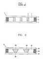
- FIG. 1is a schematic diagram illustrating a section of a typical LCD panel.
- an LCD panel 1generally comprises a lower substrate 5 , an upper substrate 3 and a liquid crystal layer 7 disposed therebetween.
- the lower substrate 5also known as the driving device array substrate
- the upper substrate 3also known as the color filter substrate, includes a color filter layer to provide color.
- the lower and upper substrates 5 and 3further include pixel electrodes and common electrodes, respectively.
- An alignment layeris formed on the lower and upper substrates 5 and 3 to align liquid crystal molecules from the liquid crystal layer 7 .
- the lower substrate 5 and the upper substrate 3are bonded to one another by a sealant 6 at peripheral regions thereof.
- a spacer 8is interposed between the lower and upper substrates 5 and 3 to maintain a constant cell-gap therebetween. Images are displayed as the driving devices in the lower substrate 5 control light transmittance through the liquid crystal layer 7 via the liquid crystal molecules disposed between the lower and upper substrates 5 and 3 .
- An LCD panelmay be fabricated using a driving device array substrate forming process to form driving devices in the lower substrate 5 and a color filter substrate forming process to form the color filter in the upper substrate 3 .
- a spacer and sealant forming processmay be employed to complete the fabrication process.
- the driving device array substrate forming processtypically includes forming a plurality of gate and data lines arranged on the lower substrate 5 to define pixel regions, forming thin film transistors (TFTs) (i.e., the driving devices) in each pixel region with each TFT being connected to a gate and data line, and forming pixel electrodes for driving the liquid crystal layer 7 when signals are applied through the TFTs.
- TFTsthin film transistors
- the color filter substrate forming processincludes forming a black matrix on the upper substrate 3 , forming a color filter on the formed black matrix, and forming a common electrode.
- the spacer 8can be a column spacer or a ball spacer. It is difficult to evenly distribute ball spacers on a substrate and maintain a uniform cell gap without reducing the aperture ratio in an LCD panel. Column spacers may be better suited for maintaining a constant cell gap and for preserving the aperture ratio, since they can be formed at predetermined positions throughout the LCD panel.
- column spacershave their own share of problems. First, they may be unable to prevent a touch inferiority defect at the surface of the LCD device. For example, when a surface portion of an LCD device is swept away, non-uniform brightness at the swept portion may generate a stain. Secondly, a press inferiority defect may occur when the surface of an LCD device is pressed under constant strength. In this case, the color filter substrate or the TFT substrate may be altered so that a corresponding stain is generated.
- a liquid crystal display deviceincludes first and second substrates and a liquid crystal layer between the first and second substrates.
- Column spacersreside between the first and second substrates to maintain a cell gap and protrusions contact corresponding column spacers where the spatial density of the protrusions varies at different positions across the first or second substrates.
- a liquid crystal display devicein another embodiment, includes first column spacers contacting the first and second substrates and second column spacers on one of the first and second substrates and spaced apart from the other of the first and second substrates.
- the spatial density of the first column spacersvaries across the first and second substrates, such that the spatial density in a center portion is less than an outer periphery portion.
- a liquid crystal display devicein yet another embodiment, includes a plurality of pixels.
- First column spacerscontact first and second substrates and second column spacers reside on one of the first and second substrates and are spaced apart from the other of the first and second substrates.
- the number of the first column spacers in the plurality of pixelsvaries across the first and second substrates, such that the number of first column spacers in the pixels in a center portion of the display is less than the number of first column spacers in the pixels in a periphery portion.
- a liquid crystal display devicein still another embodiment, includes first column spacers contacting first and second substrates.
- a plurality of pixelsinclude gate lines and data lines.
- Second column spacersreside on one of the first and second substrates and are spaced apart from the other of the first and second substrates. The number of second column spacers between the first column spacers increases along the data and gate lines from a peripheral portion of the display toward a center portion of the display.
- a liquid crystal display deviceincludes first and second substrates and a liquid crystal layer between the first and second substrates.
- Column spacersreside between the first and second substrates to maintain a cell gap.
- Protrusionscontact corresponding column spacers and the distance between the protrusions increases in a direction from a periphery of the display toward a center of the first or second substrates.
- a method for making a liquid crystal display deviceincludes forming first and second substrates and forming column spacers between the first and second substrates to maintain a cell gap. Protrusions are formed contacting corresponding column spacers, where a spatial density of the protrusions varies at different positions across the first or second substrates. A liquid crystal layer is disposed between the first and second substrates.
- FIG. 1is a sectional view schematically illustrating an LCD panel
- FIG. 2is a sectional view illustrating an LCD panel according to one aspect of the disclosure
- FIG. 3is a plan view illustrating an LCD panel according to the invention.
- FIGS. 4A and 4Bare partial sectional views along line I-I′ of FIG. 3 ;
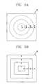
- FIGS. 5A and 5Bschematically illustrate density differences in gap spacer and pressure spacer localization according to position on an LCD panel
- FIGS. 6A-6Care graphs illustrating the density of the protrusions in the LCD panel according to the present invention.
- FIGS. 7A-7Care views illustrating the LCD panel having the protrusions and the column spacers according to the present invention.
- Touch inferioritymay be generated on an LCD device due to contact between column spacers and substrates during touching. That is, contact between a column spacer and a substrate may generate a frictional force therebetween. If the substrate is negatively impacted by these frictional forces, the liquid crystal molecules may not recover their original state and a stain may be generated in the touched portion.
- the touch inferioritycan be minimized or prevented by reducing the number of column spacers in contact with the substrates.
- Press inferioritymay be generated when pressure is applied to the substrates so as to produce changes in the color filter substrate and/or the thin film transistor (TFT) substrate. Press inferiority can be minimized or prevented by maximizing the number of column spacers so that when the pressure is applied, changes to the color filter substrate and/or the TFT substrate are prevented.
- TFTthin film transistor
- Touch inferiority and press inferiorityoperate by opposing principles.
- the spatial density of column spacersis increased, the contact areas between the column spacers and substrates is increased, thereby resulting in increased touch inferiority.
- press inferiorityis reduced.
- the spatial density of column spacersis reduced, the contact areas between the column spacers and substrates is decreased, thereby resulting in reduced touch inferiority.
- the substratesmay be altered, increasing press inferiority.
- touch inferiority and press inferiorityit is difficult to simultaneously reduce or prevent both phenomena. In other words, one cannot simply adjust the number of column spacers or their spatial density to simultaneously reduce both touch inferiority and press inferiority.
- the present inventionprovides column spacers to minimize touch inferiority and press inferiority.
- the column spacersare illustrated in FIG. 2 .
- a sealant 106is used to bond a lower substrate 105 with driving device arrays such as TFTs to an upper substrate 103 having a color filter.
- a liquid crystal layer 107is interposed between the lower and upper substrate 105 and 103 .
- On the upper substrate 103a plurality of first column spacers 108 and second column spacers 109 are formed. At this time, the first column spacers 108 and the second column spacers 109 are spaced from the lower substrate 105 in a predetermined distance.
- a plurality of protrusions 118are formed at the corresponding region to the first column spacers 108 . As shown in FIG. 2 , the first column spacers are contacted with the protrusions 118 , but the second column spacers 109 are separated from the lower substrate 105 .
- the first column spacers 108are contacted with the protrusions on the lower substrate 105 to maintain a constant cell gap between the upper and second substrates 103 and 105 .
- the combination of the first column spacers 108 the protrusion 118function as a gap spacer to maintain the constant cell gap.
- the second column spacers 109are spaced from the lower substrate 105 at a predetermined distance, the second column spacers 109 are not in contact with the lower substrate 105 .
- the second column spacers 109are brought in contact with the lower substrate 105 so that the distortion of the upper substrate 103 and the lower substrate 105 is prevented.
- the second column spacer 109function as pressure spacers.
- the first column spacers 108 and the second column spacers 109are formed on the upper substrate 103 by the same material such as an organic material in the same process, and the protrusions 118 are formed on the lower substrate 105 by a different process from that of the column spacers 108 and 109 . That is, the first and second column spacers 108 and 109 have substantially same structure. Thus, both first and second column spacer 108 and 109 are arranged in the same spatial configuration as conventional the column spacers.
- the first column spacers 108contact the protrusions 118 , such that the first column spacers 108 maintain the cell gap of the liquid crystal display panel 101 . Since the number of the protrusions 118 is smaller than the total number of the first and second column spacers 108 and 109 , however, the number of the gap spacers (that is, the combination of the first column spacers 108 and the protrusions 118 ) to maintain the cell gap is smaller than the number of the prior art gap spacers (that is, the conventional column spacers of the prior art). Therefore, the number of the column spacers in contact with the lower substrate is decreased compared with the prior art column spacers, so that the contact area between the column spacers and the lower substrate is decrease.
- the contact area between the column spacers and the lower substrate 105is further decreased compared with the contact area of prior art column spacers. In the liquid crystal panel of this invention, accordingly, the touch inferiority may be effectively prevented.
- the second column spacers 109are then brought in contacted with the lower substrate 105 and function as pressure spacers when the first and second substrates 103 and 105 are pressed, the press inferiority caused by the pressure may be effectively prevented.
- the first column spacers 108are in contact with the protrusions 118 to maintain the cell gap of the liquid crystal display panel 101 . Comparing with the prior art, thus, the number of the column spacers in contact with the lower substrate is decreased so that the touch inferiority may be prevented. Further, when pressure is applied to the upper substrate 103 and the lower substrate 105 , the first column spacers 108 are also in contact with the protrusions 118 and the second column spacers 109 are also in contact with the lower substrate 105 , so that press inferiority may be prevented. In other word, since all column spacers 108 and 109 are in contact with the lower substrate 105 when pressure is graded to the upper and lower substrate the press inferiority may be prevented.
- FIG. 3is a plan view of a liquid crystal display device having the column spacers 108 and 109 of this invention.
- an in-plane switching mode liquid crystal display deviceis shown in figure as one example of the invention, other types liquid crystal display devices such as a Twisted Nematic mode and a Vertical Alignment mode liquid crystal display device, and the like, may be adapted to the invention.
- the liquid crystal display deviceincludes a plurality of pixels defined by a plurality of gate lines 130 and data lines 135 and a thin film transistor 150 is disposed at each pixel.
- the thin film transistor 150includes a gate electrode 151 connected to the gate line 130 to which a scan signal is applied, a semiconductor layer 152 on the gate electrode 130 to be activated by the scan signal applied to the gate electrode 130 to form a channel layer, and a source and drain electrodes 153 and 154 on the semiconductor layer 152 to transmit the image signal from the data line 135 to the pixel.
- At least one common electrode 162 and pixel electrode 164are parallel disposed in the pixel to generate an electric field parallel to the surface of the substrate.
- a common line 137 connected to the common electrode 162 and a pixel electrode line 138 connected to the pixel electrode 164are disposed in the pixel.
- the common line 137 and the pixel electrode line 138overlap to generate a storage capacitance.
- a plurality of column spacers 108 and 109are formed over the gate line 130 . Although only one column spacer is formed in each pixel in FIG. 3 , alternatively two column spacers may be formed in each pixel or only one column spacer may be formed in at least two pixels.
- the protrusions 118are formed over the gate line 130 to be contact with the first column spacers 108 in order to maintain the constant cell gap. Although only one protrusion 118 is disposed in every two pixels in FIG. 3 , alternatively one protrusion 118 may be disposed in each pixel or at least two protrusions 118 may be formed in each pixel.
- first column spacers 108 and the protrusions 118act as the gap spacer and the second column spacers 109 which is not contacted with the protrusions 118 acts as pressure spacers.
- the gap spacers and the pressure spacersare alternatively disposed in the pixels.
- the gap spacers and the pressure spacersare distributed in the whole area of the substrates 103 and 105 to maintain the constant cell gap and to prevent the touch inferiority and the press inferiority.
- the column spacers 108 and 109 and the protrusions 118are formed over the gate line 130 in FIG. 3 , alternatively the column spacers 108 and 109 and the protrusions 118 may be formed over the data line 135 or in the cross region of the gate line 130 and the data line 135 .
- FIGS. 4A and 4Bare sectional views along the I-I′ line of FIG. 3 illustrating the structure of the column spacers 108 and 109 and the protrusions 118 of the LCD panel according to the illustrated embodiment.
- the upper substrateis a color filter substrate having a color filter (not shown);
- the lower substrateis a TFT substrate having a plurality of TFTs.
- the illustrated TFTincludes a gate electrode 151 on the lower substrate 105 , a gate insulating layer 162 on the lower substrate 105 , a semiconductor layer 152 on the insulation layer 162 , and a source electrode 153 and a drain electrode 154 on the semiconductor layer 153 .
- the protrusion 118includes a semiconductor layer 118 A on the gate insulating layer 162 and a metal layer 118 B on the semiconductor layer 118 A.
- a passivation layer 164is formed over the TFT and the protrusion 118 .
- the semiconductor layer 118 A of the protrusion 118may be formed by the same process as the semiconductor layer 152 of the TFT.
- the metal layer 118 Bmay be formed by the same process as the source electrode 153 and the drain electrode 154 of the TFT. Though the semiconductor layer 118 A and the metal layer 118 B may be formed by different processes than the TFT, the protrusion 118 and the TFT may be formed by the same process.
- the protrusion 118may be formed from semiconductor material or metallic material.
- the first column spacers 108 and the second column spacers 109are formed on the upper substrate 103 .
- the first column spacers 108 and the second column spacers 109are formed from organic material by common or separate processes.
- the protrusion 118may be formed on the passivation layer 164 of the lower substrate 105 .
- the protrusion 118may be formed from organic or metallic materials.
- the first column spacers 108may directly contact the lower substrate 105 without the protrusion 118 . In this case, the sectional area of the end portion contacting the lower substrate 105 may be reduced to decrease the frictional force between the surface of the lower substrate 105 and the first column spacers 108 .
- an LCD panelmay be configured so that the protrusions 118 are localized at different densities according to position on an LCD panel.
- the degree of the touch inferiority and the press inferiorityis different at the central region and the edge region of the LCD panel.
- the touch inferiorityis maximum at the central region of the LCD panel and decreases toward to the edge region of the LCD panel.
- the number (or density) of the gap spacers causing the touch inferiorityis highest at the central region and decreases toward to the central region from the edge region to minimize the touch inferiority.
- press inferiorityis maximum at the central region of the LCD panel and decreases toward to the edge region of the LCD panel.
- the number (or density) of the pressure spacers to be contact with the substrates by the pressure inferiorityis highest at the central region and decreases toward to the central region from the edge region to minimize the press inferiority.
- the gap spacers and the press spacersare formed to have different density (or number) according to the position on the LCD panel and thereby the touch inferiority and the press inferiority may be prevented.
- the gap spacer and the press spacerare defined by the protrusions 118 . That is, the first column spacers 108 act as the gap spacer because they are contacting with protrusions 118 and the second column spacers 109 act as the press spacer because they are not contacted with the protrusions 118 . Since the column spacers 108 and 109 are uniformly distributed in the LCD panel, the density (or number) of the gap spacer and the press spacer are dependent upon the density (or number) of the protrusion 118 .
- the density (or number) of the protrusions 118is decreased toward to the central region from the edge region and the density (or number) of the gap spacer is also decreased toward to the central region. Further, because there are fewer protrusions, the density (or number) of press spaces increases toward to the central region.
- FIGS. 5A and 5Bare views indicating conceptually the density of the protrusions 118 .
- the protrusions 118are positioned at higher spatial densities “a” at the edge region and at decreasing spatial densities near the central region of the LCD panel as shown in FIGS. 5A and 5B (namely, a 1 ⁇ a 2 ⁇ a 3 ⁇ a 4 , here, each of a 1 , a 2 , a 3 and a 4 denotes a protrusion density at regions I, II, III and IV divided in the LCD panel).
- the density regionsmay be defined by circular or square shapes as shown in FIGS. 5A and 5B , respectively. Selection of the square or circular shapes may depend on the size of a fabricated LCD panel 101 or an aspect ratio.
- the density regions of the LCD panel 101need not be limited to four regions, however; instead, they may be divided by essentially any plurality of density regions.
- the LCD panelBy configuring the LCD panel to have different distributions of the protrusions 118 depending on LCD panel location to have different distributions of the gap spacers and the pressure spacers, it is possible to simultaneously reduce both touch inferiority and press inferiority in an LCD panel.
- the density of the protrusions 118may be increasing in various configurations toward the edge region from the central region of the LCD panel.
- the density of the protrusions 118may be linearly or non-linearly varied.
- the variation of the density of the protrusions 118 in the LCD panelmeans a variation of the number of the protrusions 118 and a variation of the distance between the neighboring protrusions 118 . That is, the increase in density of the protrusions 118 at the edge region of the LCD panel means an increase in the number of the protrusions 118 and decrease in the distance between the neighboring protrusions at the corresponding region. Further, the decrease of density of the protrusions 118 at the central region of the LCD panel means a decrease in the number of the protrusions 118 and an increase in the distance between the neighboring protrusions at the corresponding region.
- FIGS. 6A-6Care graphs illustrating the density of the protrusions 118 in an LCD panel arranged in accordance with an embodiment of the invention and FIGS. 7A-7C are views illustrating an LCD panel having the protrusions 118 and the column spacers 108 and 109 .
- FIGS. 6A-6Care graphs illustrating the density of the protrusions 118 in an LCD panel arranged in accordance with an embodiment of the invention
- FIGS. 7A-7Care views illustrating an LCD panel having the protrusions 118 and the column spacers 108 and 109 .
- the figuresare drawn to describe conceptually the invention, only the pixels are drawn without the detail structure of the LCD panel. That is, the figures includes only the pixels arranged in the vertical and horizontal directions and the protrusions and the column spacers therein without the detailed structure.
- the LCD panel of this inventionincludes IPS mode, TN mode, and VA mode LCD panels.
- the column spacers 108 and 109 and the protrusions 118are disposed within the pixels in figures, the column spacers 108 and 109 and the protrusions 118 can be disposed over the gate line, over the data line, and at the cross region of the gate line and the data line.
- the density of the protrusions 118may be linearly increased toward the edge region from the central region of the LCD panel (where the origin represents the center of the LCD panel). Accordingly, the density of the protrusions 118 is linearly increased, as the distance d from the central region is increased.
- the linear variation of the density of the protrusions 118is shown in FIG. 7A .
- the column spacers 108 and 109are disposed in each pixel and the protrusions 118 are disposed in predetermined pixels to form the gap spacers. In this case, the distance between the neighboring protrusions 118 is linearly decreased and the number of the protrusions 118 is linearly increased toward to the edge region from the central region.
- the density of the gap spacersmay be linearly increased toward to the edge region from the central region of the LCD panel.
- the density of the protrusions 118 of this inventionmay exponentially increase toward the edge region from the central region of the LCD panel.
- the density of the protrusions 118is exponentially increased, as the distance d from the central region is increased.
- the distance between the neighboring protrusions 118is exponentially decreased and the number of the protrusions 118 is exponentially increased toward to the edge region from the central region.
- the density of the protrusions 118may logarithmically increase toward the edge region from the central region of the LCD panel.
- the density of the protrusions 118is logarithmically increased, as the distance d from the central region is increased.
- the distance between the neighboring protrusions 118is logarithmically decreased and the number of the protrusions 118 is logarithmically increased toward to the edge region from the central region.
Landscapes
- Physics & Mathematics (AREA)
- Nonlinear Science (AREA)
- Mathematical Physics (AREA)
- Chemical & Material Sciences (AREA)
- Crystallography & Structural Chemistry (AREA)
- General Physics & Mathematics (AREA)
- Optics & Photonics (AREA)
- Liquid Crystal (AREA)
Abstract
Description
Claims (41)
Applications Claiming Priority (6)
| Application Number | Priority Date | Filing Date | Title |
|---|---|---|---|
| KR20050136115 | 2005-12-30 | ||
| KR10-2005-0136115 | 2005-12-30 | ||
| KR136115/2005 | 2005-12-30 | ||
| KR10-2006-0043314 | 2006-05-15 | ||
| KR1020060043314AKR101343490B1 (en) | 2005-12-30 | 2006-05-15 | Liquid crystal display device |
| KR43314/2006 | 2006-05-15 |
Publications (2)
| Publication Number | Publication Date |
|---|---|
| US20070153215A1 US20070153215A1 (en) | 2007-07-05 |
| US7738068B2true US7738068B2 (en) | 2010-06-15 |
Family
ID=38223981
Family Applications (1)
| Application Number | Title | Priority Date | Filing Date |
|---|---|---|---|
| US11/477,266Active2029-04-15US7738068B2 (en) | 2005-12-30 | 2006-06-29 | Liquid crystal display device |
Country Status (1)
| Country | Link |
|---|---|
| US (1) | US7738068B2 (en) |
Cited By (4)
| Publication number | Priority date | Publication date | Assignee | Title |
|---|---|---|---|---|
| US20150268504A1 (en)* | 2014-03-20 | 2015-09-24 | Japan Display Inc. | Liquid crystal display device |
| US9417754B2 (en) | 2011-08-05 | 2016-08-16 | P4tents1, LLC | User interface system, method, and computer program product |
| US9810954B2 (en) | 2014-01-21 | 2017-11-07 | Boe Technology Group Co., Ltd. | Display panel with primary spacer and secondary spacer and method for manufacturing the same and display device |
| US10082706B2 (en) | 2016-01-06 | 2018-09-25 | Samsung Display Co. Ltd. | Liquid crystal display device |
Families Citing this family (11)
| Publication number | Priority date | Publication date | Assignee | Title |
|---|---|---|---|---|
| KR101137842B1 (en)* | 2005-09-23 | 2012-04-20 | 엘지디스플레이 주식회사 | Liquid Crystal Display Device and Method for Manufacturing the Same |
| CN100595654C (en)* | 2007-12-29 | 2010-03-24 | 昆山龙腾光电有限公司 | Liquid crystal display panel |
| KR101326580B1 (en)* | 2008-06-27 | 2013-11-08 | 엘지디스플레이 주식회사 | Liquide crystal display device and method for fabricating the same |
| CN102375271B (en)* | 2010-08-16 | 2015-02-25 | 上海天马微电子有限公司 | Liquid crystal display panel, liquid crystal display and manufacturing method of liquid crystal display panel |
| KR101420686B1 (en)* | 2011-11-17 | 2014-07-21 | 엘지디스플레이 주식회사 | Image display device including barrier cell and method of fabricating the same |
| KR101396943B1 (en)* | 2012-06-25 | 2014-05-19 | 엘지디스플레이 주식회사 | Liquid crystal display device and manufacturing method |
| CN103792735B (en)* | 2014-01-22 | 2016-08-24 | 京东方科技集团股份有限公司 | Chock insulator matter, the liquid crystal panel applying it and display device |
| CN105116631A (en)* | 2015-09-23 | 2015-12-02 | 京东方科技集团股份有限公司 | Display panel and display device |
| JP2017187530A (en)* | 2016-04-01 | 2017-10-12 | 株式会社ジャパンディスプレイ | Liquid crystal display |
| JP7038537B2 (en)* | 2017-12-14 | 2022-03-18 | 株式会社ジャパンディスプレイ | Liquid crystal display device and its manufacturing method |
| CN119781197B (en)* | 2024-12-30 | 2025-09-12 | 绵阳惠科光电科技有限公司 | Display panel and display device |
Citations (3)
| Publication number | Priority date | Publication date | Assignee | Title |
|---|---|---|---|---|
| CN1661425A (en) | 2004-02-25 | 2005-08-31 | Lg.菲利浦Lcd株式会社 | Liquid crystal display device and manufacturing method thereof |
| CN1696776A (en) | 2004-05-10 | 2005-11-16 | 鸿富锦精密工业(深圳)有限公司 | Faceplate of liquid crystal display |
| US7375788B2 (en)* | 2004-04-30 | 2008-05-20 | Innolux Display Corp. | Liquid crystal display device with hollow semi-columnar photo spacers |
- 2006
- 2006-06-29USUS11/477,266patent/US7738068B2/enactiveActive
Patent Citations (3)
| Publication number | Priority date | Publication date | Assignee | Title |
|---|---|---|---|---|
| CN1661425A (en) | 2004-02-25 | 2005-08-31 | Lg.菲利浦Lcd株式会社 | Liquid crystal display device and manufacturing method thereof |
| US7375788B2 (en)* | 2004-04-30 | 2008-05-20 | Innolux Display Corp. | Liquid crystal display device with hollow semi-columnar photo spacers |
| CN1696776A (en) | 2004-05-10 | 2005-11-16 | 鸿富锦精密工业(深圳)有限公司 | Faceplate of liquid crystal display |
Non-Patent Citations (1)
| Title |
|---|
| Office Action issued in corresponding Chinese Patent Application No. 200610095971.4; issued Jul. 4, 2008. |
Cited By (60)
| Publication number | Priority date | Publication date | Assignee | Title |
|---|---|---|---|---|
| US10540039B1 (en) | 2011-08-05 | 2020-01-21 | P4tents1, LLC | Devices and methods for navigating between user interface |
| US10649579B1 (en) | 2011-08-05 | 2020-05-12 | P4tents1, LLC | Devices, methods, and graphical user interfaces for manipulating user interface objects with visual and/or haptic feedback |
| US10013095B1 (en) | 2011-08-05 | 2018-07-03 | P4tents1, LLC | Multi-type gesture-equipped touch screen system, method, and computer program product |
| US10031607B1 (en) | 2011-08-05 | 2018-07-24 | P4tents1, LLC | System, method, and computer program product for a multi-pressure selection touch screen |
| US9417754B2 (en) | 2011-08-05 | 2016-08-16 | P4tents1, LLC | User interface system, method, and computer program product |
| US11740727B1 (en) | 2011-08-05 | 2023-08-29 | P4Tents1 Llc | Devices, methods, and graphical user interfaces for manipulating user interface objects with visual and/or haptic feedback |
| US11061503B1 (en) | 2011-08-05 | 2021-07-13 | P4tents1, LLC | Devices, methods, and graphical user interfaces for manipulating user interface objects with visual and/or haptic feedback |
| US10996787B1 (en) | 2011-08-05 | 2021-05-04 | P4tents1, LLC | Gesture-equipped touch screen system, method, and computer program product |
| US10133397B1 (en) | 2011-08-05 | 2018-11-20 | P4tents1, LLC | Tri-state gesture-equipped touch screen system, method, and computer program product |
| US10146353B1 (en) | 2011-08-05 | 2018-12-04 | P4tents1, LLC | Touch screen system, method, and computer program product |
| US10156921B1 (en) | 2011-08-05 | 2018-12-18 | P4tents1, LLC | Tri-state gesture-equipped touch screen system, method, and computer program product |
| US10162448B1 (en) | 2011-08-05 | 2018-12-25 | P4tents1, LLC | System, method, and computer program product for a pressure-sensitive touch screen for messages |
| US10203794B1 (en) | 2011-08-05 | 2019-02-12 | P4tents1, LLC | Pressure-sensitive home interface system, method, and computer program product |
| US10209807B1 (en) | 2011-08-05 | 2019-02-19 | P4tents1, LLC | Pressure sensitive touch screen system, method, and computer program product for hyperlinks |
| US10209806B1 (en) | 2011-08-05 | 2019-02-19 | P4tents1, LLC | Tri-state gesture-equipped touch screen system, method, and computer program product |
| US10209809B1 (en) | 2011-08-05 | 2019-02-19 | P4tents1, LLC | Pressure-sensitive touch screen system, method, and computer program product for objects |
| US10209808B1 (en) | 2011-08-05 | 2019-02-19 | P4tents1, LLC | Pressure-based interface system, method, and computer program product with virtual display layers |
| US10222892B1 (en) | 2011-08-05 | 2019-03-05 | P4tents1, LLC | System, method, and computer program product for a multi-pressure selection touch screen |
| US10222893B1 (en) | 2011-08-05 | 2019-03-05 | P4tents1, LLC | Pressure-based touch screen system, method, and computer program product with virtual display layers |
| US10222895B1 (en) | 2011-08-05 | 2019-03-05 | P4tents1, LLC | Pressure-based touch screen system, method, and computer program product with virtual display layers |
| US10222894B1 (en) | 2011-08-05 | 2019-03-05 | P4tents1, LLC | System, method, and computer program product for a multi-pressure selection touch screen |
| US10222891B1 (en) | 2011-08-05 | 2019-03-05 | P4tents1, LLC | Setting interface system, method, and computer program product for a multi-pressure selection touch screen |
| US10275087B1 (en) | 2011-08-05 | 2019-04-30 | P4tents1, LLC | Devices, methods, and graphical user interfaces for manipulating user interface objects with visual and/or haptic feedback |
| US10275086B1 (en) | 2011-08-05 | 2019-04-30 | P4tents1, LLC | Gesture-equipped touch screen system, method, and computer program product |
| US10338736B1 (en) | 2011-08-05 | 2019-07-02 | P4tents1, LLC | Devices, methods, and graphical user interfaces for manipulating user interface objects with visual and/or haptic feedback |
| US10345961B1 (en) | 2011-08-05 | 2019-07-09 | P4tents1, LLC | Devices and methods for navigating between user interfaces |
| US10365758B1 (en) | 2011-08-05 | 2019-07-30 | P4tents1, LLC | Devices, methods, and graphical user interfaces for manipulating user interface objects with visual and/or haptic feedback |
| US10386960B1 (en) | 2011-08-05 | 2019-08-20 | P4tents1, LLC | Devices, methods, and graphical user interfaces for manipulating user interface objects with visual and/or haptic feedback |
| US10013094B1 (en) | 2011-08-05 | 2018-07-03 | P4tents1, LLC | System, method, and computer program product for a multi-pressure selection touch screen |
| US10521047B1 (en) | 2011-08-05 | 2019-12-31 | P4tents1, LLC | Gesture-equipped touch screen system, method, and computer program product |
| US10120480B1 (en) | 2011-08-05 | 2018-11-06 | P4tents1, LLC | Application-specific pressure-sensitive touch screen system, method, and computer program product |
| US10551966B1 (en) | 2011-08-05 | 2020-02-04 | P4tents1, LLC | Gesture-equipped touch screen system, method, and computer program product |
| US10592039B1 (en) | 2011-08-05 | 2020-03-17 | P4tents1, LLC | Gesture-equipped touch screen system, method, and computer program product for displaying multiple active applications |
| US10606396B1 (en) | 2011-08-05 | 2020-03-31 | P4tents1, LLC | Gesture-equipped touch screen methods for duration-based functions |
| US10642413B1 (en) | 2011-08-05 | 2020-05-05 | P4tents1, LLC | Gesture-equipped touch screen system, method, and computer program product |
| US10649571B1 (en) | 2011-08-05 | 2020-05-12 | P4tents1, LLC | Devices, methods, and graphical user interfaces for manipulating user interface objects with visual and/or haptic feedback |
| US10649578B1 (en) | 2011-08-05 | 2020-05-12 | P4tents1, LLC | Gesture-equipped touch screen system, method, and computer program product |
| US10649581B1 (en) | 2011-08-05 | 2020-05-12 | P4tents1, LLC | Devices, methods, and graphical user interfaces for manipulating user interface objects with visual and/or haptic feedback |
| US10649580B1 (en) | 2011-08-05 | 2020-05-12 | P4tents1, LLC | Devices, methods, and graphical use interfaces for manipulating user interface objects with visual and/or haptic feedback |
| US10534474B1 (en) | 2011-08-05 | 2020-01-14 | P4tents1, LLC | Gesture-equipped touch screen system, method, and computer program product |
| US10656757B1 (en) | 2011-08-05 | 2020-05-19 | P4tents1, LLC | Gesture-equipped touch screen system, method, and computer program product |
| US10656754B1 (en) | 2011-08-05 | 2020-05-19 | P4tents1, LLC | Devices and methods for navigating between user interfaces |
| US10656752B1 (en) | 2011-08-05 | 2020-05-19 | P4tents1, LLC | Gesture-equipped touch screen system, method, and computer program product |
| US10656753B1 (en) | 2011-08-05 | 2020-05-19 | P4tents1, LLC | Gesture-equipped touch screen system, method, and computer program product |
| US10656756B1 (en) | 2011-08-05 | 2020-05-19 | P4tents1, LLC | Gesture-equipped touch screen system, method, and computer program product |
| US10656755B1 (en) | 2011-08-05 | 2020-05-19 | P4tents1, LLC | Gesture-equipped touch screen system, method, and computer program product |
| US10656759B1 (en) | 2011-08-05 | 2020-05-19 | P4tents1, LLC | Devices, methods, and graphical user interfaces for manipulating user interface objects with visual and/or haptic feedback |
| US10656758B1 (en) | 2011-08-05 | 2020-05-19 | P4tents1, LLC | Gesture-equipped touch screen system, method, and computer program product |
| US10664097B1 (en) | 2011-08-05 | 2020-05-26 | P4tents1, LLC | Devices, methods, and graphical user interfaces for manipulating user interface objects with visual and/or haptic feedback |
| US10671212B1 (en) | 2011-08-05 | 2020-06-02 | P4tents1, LLC | Gesture-equipped touch screen system, method, and computer program product |
| US10671213B1 (en) | 2011-08-05 | 2020-06-02 | P4tents1, LLC | Devices, methods, and graphical user interfaces for manipulating user interface objects with visual and/or haptic feedback |
| US10725581B1 (en) | 2011-08-05 | 2020-07-28 | P4tents1, LLC | Devices, methods and graphical user interfaces for manipulating user interface objects with visual and/or haptic feedback |
| US10782819B1 (en) | 2011-08-05 | 2020-09-22 | P4tents1, LLC | Gesture-equipped touch screen system, method, and computer program product |
| US10788931B1 (en) | 2011-08-05 | 2020-09-29 | P4tents1, LLC | Devices, methods, and graphical user interfaces for manipulating user interface objects with visual and/or haptic feedback |
| US10838542B1 (en) | 2011-08-05 | 2020-11-17 | P4tents1, LLC | Gesture-equipped touch screen system, method, and computer program product |
| US10936114B1 (en) | 2011-08-05 | 2021-03-02 | P4tents1, LLC | Gesture-equipped touch screen system, method, and computer program product |
| US9810954B2 (en) | 2014-01-21 | 2017-11-07 | Boe Technology Group Co., Ltd. | Display panel with primary spacer and secondary spacer and method for manufacturing the same and display device |
| US9798194B2 (en)* | 2014-03-20 | 2017-10-24 | Japan Display Inc. | Liquid crystal display device |
| US20150268504A1 (en)* | 2014-03-20 | 2015-09-24 | Japan Display Inc. | Liquid crystal display device |
| US10082706B2 (en) | 2016-01-06 | 2018-09-25 | Samsung Display Co. Ltd. | Liquid crystal display device |
Also Published As
| Publication number | Publication date |
|---|---|
| US20070153215A1 (en) | 2007-07-05 |
Similar Documents
| Publication | Publication Date | Title |
|---|---|---|
| US7738068B2 (en) | Liquid crystal display device | |
| KR101343490B1 (en) | Liquid crystal display device | |
| US6335780B1 (en) | LCD with protrusion structures for axially symmetrically aligning liquid crystal in regions smaller than 70 μm×70 μm | |
| US8253916B2 (en) | Liquid crystal display device | |
| US7623212B2 (en) | Liquid crystal display device | |
| US9638975B2 (en) | Method for manufacturing COA liquid crystal panel comprising color resist blocks having first and second intersection zones and COA liquid crystal panel | |
| US7701540B2 (en) | Liquid crystal display device and method for manufacturing the same | |
| US20060227276A1 (en) | In-plane switching mode liquid crystal display device | |
| US20140184972A1 (en) | Display panel and liquid crystal display including the same | |
| KR20050107900A (en) | In plane switching mode liquid crystal display device having improved contrast ratio | |
| US20030128312A1 (en) | Liquid crystal display | |
| US6940571B2 (en) | Liquid crystal display device | |
| KR20160019036A (en) | Display panel | |
| US7525622B2 (en) | Liquid crystal display device and method for fabricating the same | |
| US6897931B2 (en) | In-plane switching mode liquid crystal display device and method for fabricating the same | |
| WO2019062395A1 (en) | Display panel, display device, and driving method thereof | |
| US20070058126A1 (en) | Liquid crystal display panel and manufacturing method thereof | |
| US7420640B2 (en) | In-plane switching mode liquid crystal device and method for manufacturing the same | |
| CN114077108B (en) | A display panel and display device | |
| US20040263737A1 (en) | Method of fabricating liquid crystal display device having various driving modes | |
| JP5491892B2 (en) | Liquid crystal display | |
| US20210088822A1 (en) | Ips type display panel and display device | |
| CN115016183B (en) | Display panel and display device | |
| CN114755857B (en) | Display panel and display device | |
| KR20050034957A (en) | Method of fabricating vertical alignment liquid crystal display panel having various sizes |
Legal Events
| Date | Code | Title | Description |
|---|---|---|---|
| AS | Assignment | Owner name:LG. PHILIPS LCD CO., LTD.,KOREA, REPUBLIC OF Free format text:ASSIGNMENT OF ASSIGNORS INTEREST;ASSIGNOR:LEE, TAE-RIM;REEL/FRAME:018063/0566 Effective date:20060626 Owner name:LG. PHILIPS LCD CO., LTD., KOREA, REPUBLIC OF Free format text:ASSIGNMENT OF ASSIGNORS INTEREST;ASSIGNOR:LEE, TAE-RIM;REEL/FRAME:018063/0566 Effective date:20060626 | |
| AS | Assignment | Owner name:LG DISPLAY CO., LTD., KOREA, REPUBLIC OF Free format text:CHANGE OF NAME;ASSIGNOR:LG. PHILIPS CO., LTD.;REEL/FRAME:020963/0710 Effective date:20080229 Owner name:LG DISPLAY CO., LTD.,KOREA, REPUBLIC OF Free format text:CHANGE OF NAME;ASSIGNOR:LG. PHILIPS CO., LTD.;REEL/FRAME:020963/0710 Effective date:20080229 | |
| FEPP | Fee payment procedure | Free format text:PAYOR NUMBER ASSIGNED (ORIGINAL EVENT CODE: ASPN); ENTITY STATUS OF PATENT OWNER: LARGE ENTITY | |
| STCF | Information on status: patent grant | Free format text:PATENTED CASE | |
| FPAY | Fee payment | Year of fee payment:4 | |
| MAFP | Maintenance fee payment | Free format text:PAYMENT OF MAINTENANCE FEE, 8TH YEAR, LARGE ENTITY (ORIGINAL EVENT CODE: M1552) Year of fee payment:8 | |
| MAFP | Maintenance fee payment | Free format text:PAYMENT OF MAINTENANCE FEE, 12TH YEAR, LARGE ENTITY (ORIGINAL EVENT CODE: M1553); ENTITY STATUS OF PATENT OWNER: LARGE ENTITY Year of fee payment:12 |