US7737871B2 - MCU with integrated voltage isolator to provide a galvanic isolation between input and output - Google Patents
MCU with integrated voltage isolator to provide a galvanic isolation between input and outputDownload PDFInfo
- Publication number
- US7737871B2 US7737871B2US12/164,998US16499808AUS7737871B2US 7737871 B2US7737871 B2US 7737871B2US 16499808 AUS16499808 AUS 16499808AUS 7737871 B2US7737871 B2US 7737871B2
- Authority
- US
- United States
- Prior art keywords
- data
- die
- isolation
- parallel
- microcontroller unit
- Prior art date
- Legal status (The legal status is an assumption and is not a legal conclusion. Google has not performed a legal analysis and makes no representation as to the accuracy of the status listed.)
- Expired - Lifetime, expires
Links
Images


Classifications
- H—ELECTRICITY
- H01—ELECTRIC ELEMENTS
- H01L—SEMICONDUCTOR DEVICES NOT COVERED BY CLASS H10
- H01L23/00—Details of semiconductor or other solid state devices
- H01L23/58—Structural electrical arrangements for semiconductor devices not otherwise provided for, e.g. in combination with batteries
- H01L23/64—Impedance arrangements
- H01L23/66—High-frequency adaptations
- H—ELECTRICITY
- H01—ELECTRIC ELEMENTS
- H01L—SEMICONDUCTOR DEVICES NOT COVERED BY CLASS H10
- H01L23/00—Details of semiconductor or other solid state devices
- H01L23/48—Arrangements for conducting electric current to or from the solid state body in operation, e.g. leads, terminal arrangements ; Selection of materials therefor
- H—ELECTRICITY
- H01—ELECTRIC ELEMENTS
- H01L—SEMICONDUCTOR DEVICES NOT COVERED BY CLASS H10
- H01L24/00—Arrangements for connecting or disconnecting semiconductor or solid-state bodies; Methods or apparatus related thereto
- H01L24/01—Means for bonding being attached to, or being formed on, the surface to be connected, e.g. chip-to-package, die-attach, "first-level" interconnects; Manufacturing methods related thereto
- H01L24/02—Bonding areas ; Manufacturing methods related thereto
- H01L24/04—Structure, shape, material or disposition of the bonding areas prior to the connecting process
- H01L24/06—Structure, shape, material or disposition of the bonding areas prior to the connecting process of a plurality of bonding areas
- H—ELECTRICITY
- H01—ELECTRIC ELEMENTS
- H01L—SEMICONDUCTOR DEVICES NOT COVERED BY CLASS H10
- H01L24/00—Arrangements for connecting or disconnecting semiconductor or solid-state bodies; Methods or apparatus related thereto
- H01L24/01—Means for bonding being attached to, or being formed on, the surface to be connected, e.g. chip-to-package, die-attach, "first-level" interconnects; Manufacturing methods related thereto
- H01L24/42—Wire connectors; Manufacturing methods related thereto
- H01L24/47—Structure, shape, material or disposition of the wire connectors after the connecting process
- H01L24/49—Structure, shape, material or disposition of the wire connectors after the connecting process of a plurality of wire connectors
- H—ELECTRICITY
- H01—ELECTRIC ELEMENTS
- H01L—SEMICONDUCTOR DEVICES NOT COVERED BY CLASS H10
- H01L2223/00—Details relating to semiconductor or other solid state devices covered by the group H01L23/00
- H01L2223/58—Structural electrical arrangements for semiconductor devices not otherwise provided for
- H01L2223/64—Impedance arrangements
- H01L2223/66—High-frequency adaptations
- H01L2223/6605—High-frequency electrical connections
- H01L2223/6611—Wire connections
- H—ELECTRICITY
- H01—ELECTRIC ELEMENTS
- H01L—SEMICONDUCTOR DEVICES NOT COVERED BY CLASS H10
- H01L2224/00—Indexing scheme for arrangements for connecting or disconnecting semiconductor or solid-state bodies and methods related thereto as covered by H01L24/00
- H01L2224/01—Means for bonding being attached to, or being formed on, the surface to be connected, e.g. chip-to-package, die-attach, "first-level" interconnects; Manufacturing methods related thereto
- H01L2224/02—Bonding areas; Manufacturing methods related thereto
- H01L2224/04—Structure, shape, material or disposition of the bonding areas prior to the connecting process
- H01L2224/05—Structure, shape, material or disposition of the bonding areas prior to the connecting process of an individual bonding area
- H01L2224/0554—External layer
- H01L2224/0555—Shape
- H01L2224/05552—Shape in top view
- H01L2224/05554—Shape in top view being square
- H—ELECTRICITY
- H01—ELECTRIC ELEMENTS
- H01L—SEMICONDUCTOR DEVICES NOT COVERED BY CLASS H10
- H01L2224/00—Indexing scheme for arrangements for connecting or disconnecting semiconductor or solid-state bodies and methods related thereto as covered by H01L24/00
- H01L2224/01—Means for bonding being attached to, or being formed on, the surface to be connected, e.g. chip-to-package, die-attach, "first-level" interconnects; Manufacturing methods related thereto
- H01L2224/42—Wire connectors; Manufacturing methods related thereto
- H01L2224/47—Structure, shape, material or disposition of the wire connectors after the connecting process
- H01L2224/48—Structure, shape, material or disposition of the wire connectors after the connecting process of an individual wire connector
- H01L2224/4805—Shape
- H01L2224/4809—Loop shape
- H01L2224/48095—Kinked
- H—ELECTRICITY
- H01—ELECTRIC ELEMENTS
- H01L—SEMICONDUCTOR DEVICES NOT COVERED BY CLASS H10
- H01L2224/00—Indexing scheme for arrangements for connecting or disconnecting semiconductor or solid-state bodies and methods related thereto as covered by H01L24/00
- H01L2224/01—Means for bonding being attached to, or being formed on, the surface to be connected, e.g. chip-to-package, die-attach, "first-level" interconnects; Manufacturing methods related thereto
- H01L2224/42—Wire connectors; Manufacturing methods related thereto
- H01L2224/47—Structure, shape, material or disposition of the wire connectors after the connecting process
- H01L2224/48—Structure, shape, material or disposition of the wire connectors after the connecting process of an individual wire connector
- H01L2224/481—Disposition
- H01L2224/48135—Connecting between different semiconductor or solid-state bodies, i.e. chip-to-chip
- H01L2224/48137—Connecting between different semiconductor or solid-state bodies, i.e. chip-to-chip the bodies being arranged next to each other, e.g. on a common substrate
- H—ELECTRICITY
- H01—ELECTRIC ELEMENTS
- H01L—SEMICONDUCTOR DEVICES NOT COVERED BY CLASS H10
- H01L2224/00—Indexing scheme for arrangements for connecting or disconnecting semiconductor or solid-state bodies and methods related thereto as covered by H01L24/00
- H01L2224/01—Means for bonding being attached to, or being formed on, the surface to be connected, e.g. chip-to-package, die-attach, "first-level" interconnects; Manufacturing methods related thereto
- H01L2224/42—Wire connectors; Manufacturing methods related thereto
- H01L2224/47—Structure, shape, material or disposition of the wire connectors after the connecting process
- H01L2224/48—Structure, shape, material or disposition of the wire connectors after the connecting process of an individual wire connector
- H01L2224/481—Disposition
- H01L2224/48151—Connecting between a semiconductor or solid-state body and an item not being a semiconductor or solid-state body, e.g. chip-to-substrate, chip-to-passive
- H01L2224/48221—Connecting between a semiconductor or solid-state body and an item not being a semiconductor or solid-state body, e.g. chip-to-substrate, chip-to-passive the body and the item being stacked
- H01L2224/48245—Connecting between a semiconductor or solid-state body and an item not being a semiconductor or solid-state body, e.g. chip-to-substrate, chip-to-passive the body and the item being stacked the item being metallic
- H01L2224/48247—Connecting between a semiconductor or solid-state body and an item not being a semiconductor or solid-state body, e.g. chip-to-substrate, chip-to-passive the body and the item being stacked the item being metallic connecting the wire to a bond pad of the item
- H—ELECTRICITY
- H01—ELECTRIC ELEMENTS
- H01L—SEMICONDUCTOR DEVICES NOT COVERED BY CLASS H10
- H01L2224/00—Indexing scheme for arrangements for connecting or disconnecting semiconductor or solid-state bodies and methods related thereto as covered by H01L24/00
- H01L2224/01—Means for bonding being attached to, or being formed on, the surface to be connected, e.g. chip-to-package, die-attach, "first-level" interconnects; Manufacturing methods related thereto
- H01L2224/42—Wire connectors; Manufacturing methods related thereto
- H01L2224/47—Structure, shape, material or disposition of the wire connectors after the connecting process
- H01L2224/48—Structure, shape, material or disposition of the wire connectors after the connecting process of an individual wire connector
- H01L2224/481—Disposition
- H01L2224/48151—Connecting between a semiconductor or solid-state body and an item not being a semiconductor or solid-state body, e.g. chip-to-substrate, chip-to-passive
- H01L2224/48221—Connecting between a semiconductor or solid-state body and an item not being a semiconductor or solid-state body, e.g. chip-to-substrate, chip-to-passive the body and the item being stacked
- H01L2224/48245—Connecting between a semiconductor or solid-state body and an item not being a semiconductor or solid-state body, e.g. chip-to-substrate, chip-to-passive the body and the item being stacked the item being metallic
- H01L2224/48257—Connecting between a semiconductor or solid-state body and an item not being a semiconductor or solid-state body, e.g. chip-to-substrate, chip-to-passive the body and the item being stacked the item being metallic connecting the wire to a die pad of the item
- H—ELECTRICITY
- H01—ELECTRIC ELEMENTS
- H01L—SEMICONDUCTOR DEVICES NOT COVERED BY CLASS H10
- H01L2224/00—Indexing scheme for arrangements for connecting or disconnecting semiconductor or solid-state bodies and methods related thereto as covered by H01L24/00
- H01L2224/01—Means for bonding being attached to, or being formed on, the surface to be connected, e.g. chip-to-package, die-attach, "first-level" interconnects; Manufacturing methods related thereto
- H01L2224/42—Wire connectors; Manufacturing methods related thereto
- H01L2224/47—Structure, shape, material or disposition of the wire connectors after the connecting process
- H01L2224/49—Structure, shape, material or disposition of the wire connectors after the connecting process of a plurality of wire connectors
- H01L2224/491—Disposition
- H01L2224/4912—Layout
- H01L2224/49171—Fan-out arrangements
- H—ELECTRICITY
- H01—ELECTRIC ELEMENTS
- H01L—SEMICONDUCTOR DEVICES NOT COVERED BY CLASS H10
- H01L2224/00—Indexing scheme for arrangements for connecting or disconnecting semiconductor or solid-state bodies and methods related thereto as covered by H01L24/00
- H01L2224/01—Means for bonding being attached to, or being formed on, the surface to be connected, e.g. chip-to-package, die-attach, "first-level" interconnects; Manufacturing methods related thereto
- H01L2224/42—Wire connectors; Manufacturing methods related thereto
- H01L2224/47—Structure, shape, material or disposition of the wire connectors after the connecting process
- H01L2224/49—Structure, shape, material or disposition of the wire connectors after the connecting process of a plurality of wire connectors
- H01L2224/491—Disposition
- H01L2224/4912—Layout
- H01L2224/49175—Parallel arrangements
- H—ELECTRICITY
- H01—ELECTRIC ELEMENTS
- H01L—SEMICONDUCTOR DEVICES NOT COVERED BY CLASS H10
- H01L24/00—Arrangements for connecting or disconnecting semiconductor or solid-state bodies; Methods or apparatus related thereto
- H01L24/01—Means for bonding being attached to, or being formed on, the surface to be connected, e.g. chip-to-package, die-attach, "first-level" interconnects; Manufacturing methods related thereto
- H01L24/42—Wire connectors; Manufacturing methods related thereto
- H01L24/47—Structure, shape, material or disposition of the wire connectors after the connecting process
- H01L24/48—Structure, shape, material or disposition of the wire connectors after the connecting process of an individual wire connector
- H—ELECTRICITY
- H01—ELECTRIC ELEMENTS
- H01L—SEMICONDUCTOR DEVICES NOT COVERED BY CLASS H10
- H01L2924/00—Indexing scheme for arrangements or methods for connecting or disconnecting semiconductor or solid-state bodies as covered by H01L24/00
- H01L2924/0001—Technical content checked by a classifier
- H01L2924/00014—Technical content checked by a classifier the subject-matter covered by the group, the symbol of which is combined with the symbol of this group, being disclosed without further technical details
- H—ELECTRICITY
- H01—ELECTRIC ELEMENTS
- H01L—SEMICONDUCTOR DEVICES NOT COVERED BY CLASS H10
- H01L2924/00—Indexing scheme for arrangements or methods for connecting or disconnecting semiconductor or solid-state bodies as covered by H01L24/00
- H01L2924/01—Chemical elements
- H01L2924/01006—Carbon [C]
- H—ELECTRICITY
- H01—ELECTRIC ELEMENTS
- H01L—SEMICONDUCTOR DEVICES NOT COVERED BY CLASS H10
- H01L2924/00—Indexing scheme for arrangements or methods for connecting or disconnecting semiconductor or solid-state bodies as covered by H01L24/00
- H01L2924/01—Chemical elements
- H01L2924/01014—Silicon [Si]
- H—ELECTRICITY
- H01—ELECTRIC ELEMENTS
- H01L—SEMICONDUCTOR DEVICES NOT COVERED BY CLASS H10
- H01L2924/00—Indexing scheme for arrangements or methods for connecting or disconnecting semiconductor or solid-state bodies as covered by H01L24/00
- H01L2924/01—Chemical elements
- H01L2924/01015—Phosphorus [P]
- H—ELECTRICITY
- H01—ELECTRIC ELEMENTS
- H01L—SEMICONDUCTOR DEVICES NOT COVERED BY CLASS H10
- H01L2924/00—Indexing scheme for arrangements or methods for connecting or disconnecting semiconductor or solid-state bodies as covered by H01L24/00
- H01L2924/01—Chemical elements
- H01L2924/01023—Vanadium [V]
- H—ELECTRICITY
- H01—ELECTRIC ELEMENTS
- H01L—SEMICONDUCTOR DEVICES NOT COVERED BY CLASS H10
- H01L2924/00—Indexing scheme for arrangements or methods for connecting or disconnecting semiconductor or solid-state bodies as covered by H01L24/00
- H01L2924/01—Chemical elements
- H01L2924/01033—Arsenic [As]
- H—ELECTRICITY
- H01—ELECTRIC ELEMENTS
- H01L—SEMICONDUCTOR DEVICES NOT COVERED BY CLASS H10
- H01L2924/00—Indexing scheme for arrangements or methods for connecting or disconnecting semiconductor or solid-state bodies as covered by H01L24/00
- H01L2924/01—Chemical elements
- H01L2924/01082—Lead [Pb]
- H—ELECTRICITY
- H01—ELECTRIC ELEMENTS
- H01L—SEMICONDUCTOR DEVICES NOT COVERED BY CLASS H10
- H01L2924/00—Indexing scheme for arrangements or methods for connecting or disconnecting semiconductor or solid-state bodies as covered by H01L24/00
- H01L2924/10—Details of semiconductor or other solid state devices to be connected
- H01L2924/102—Material of the semiconductor or solid state bodies
- H01L2924/1025—Semiconducting materials
- H01L2924/10251—Elemental semiconductors, i.e. Group IV
- H01L2924/10253—Silicon [Si]
- H—ELECTRICITY
- H01—ELECTRIC ELEMENTS
- H01L—SEMICONDUCTOR DEVICES NOT COVERED BY CLASS H10
- H01L2924/00—Indexing scheme for arrangements or methods for connecting or disconnecting semiconductor or solid-state bodies as covered by H01L24/00
- H01L2924/10—Details of semiconductor or other solid state devices to be connected
- H01L2924/11—Device type
- H01L2924/14—Integrated circuits
- H—ELECTRICITY
- H01—ELECTRIC ELEMENTS
- H01L—SEMICONDUCTOR DEVICES NOT COVERED BY CLASS H10
- H01L2924/00—Indexing scheme for arrangements or methods for connecting or disconnecting semiconductor or solid-state bodies as covered by H01L24/00
- H01L2924/19—Details of hybrid assemblies other than the semiconductor or other solid state devices to be connected
- H01L2924/1901—Structure
- H01L2924/1904—Component type
- H01L2924/19041—Component type being a capacitor
- H—ELECTRICITY
- H01—ELECTRIC ELEMENTS
- H01L—SEMICONDUCTOR DEVICES NOT COVERED BY CLASS H10
- H01L2924/00—Indexing scheme for arrangements or methods for connecting or disconnecting semiconductor or solid-state bodies as covered by H01L24/00
- H01L2924/19—Details of hybrid assemblies other than the semiconductor or other solid state devices to be connected
- H01L2924/1901—Structure
- H01L2924/1904—Component type
- H01L2924/19042—Component type being an inductor
- H—ELECTRICITY
- H01—ELECTRIC ELEMENTS
- H01L—SEMICONDUCTOR DEVICES NOT COVERED BY CLASS H10
- H01L2924/00—Indexing scheme for arrangements or methods for connecting or disconnecting semiconductor or solid-state bodies as covered by H01L24/00
- H01L2924/19—Details of hybrid assemblies other than the semiconductor or other solid state devices to be connected
- H01L2924/1901—Structure
- H01L2924/1904—Component type
- H01L2924/19043—Component type being a resistor
- H—ELECTRICITY
- H01—ELECTRIC ELEMENTS
- H01L—SEMICONDUCTOR DEVICES NOT COVERED BY CLASS H10
- H01L2924/00—Indexing scheme for arrangements or methods for connecting or disconnecting semiconductor or solid-state bodies as covered by H01L24/00
- H01L2924/30—Technical effects
- H01L2924/301—Electrical effects
- H01L2924/30105—Capacitance
Definitions
- the present inventionis a Continuation-in-part of U.S. patent application Ser. No. 12/060,049, filed on Mar. 31, 2008, entitled, “CAPACITIVE ISOLATOR,” which is a continuation-in-part of U.S. patent application Ser. No. 11/772,178, filed on Jun. 30, 2007, entitled, “BIDIRECTIONAL MULTIPLEXED RF ISOLATOR,” which is a continuation-in-part of U.S. Pat. No. 7,302,247, issued on Nov. 27, 2007, entitled, “SPREAD SPECTRUM ISOLATOR,” which is a continuation-in-part of U.S. patent application Ser. No. 10/860,399, filed on Jun.
- the present inventionrelates to microcontroller units, and more particularly, to a microcontroller unit having an integrated voltage isolation functionality on a single chip.
- Galvanic isolationis defined as the principle of isolating functional sections of electric systems so that charge-carrying particles cannot move from one section to another, i.e. there is no electrical current flowing directly from one section to the next. Energy and/or information can still be exchanged between the sections by other means, however, such as by capacitance, induction, electromagnetic waves, optical, acoustic, or mechanical means.
- a driver on one side of the digital linktransmits information over the digital link to a detector residing on the other side of the digital link.
- the pulse transformerprovides an electromagnetically coupled transformer between the driver and the detector.
- the pulse transformergenerates a pulse output in response to a provided input from the driver.
- the input from the driverconsists of two pulses, each pulse consisting of a rising edge and a falling edge. In response to a rising edge, the output of the pulse transformer generates a positive pulse. The falling edge of the pulse generates a negative pulse.
- the pulse transformer circuithas a number of deficiencies.
- the magneto resistive couplerconsists of a resistor and an associated transformer.
- the resistorhas a resistance value that changes responsive to the magnetic flux about the resistor.
- the transformer detectorutilizes a Wheatstone bridge to detect the magnetic flux of the resistor and determine the transmitted data.
- Opto couplersare the dominant voltage isolation technology used in the market today. The use of opto couplers is mandated by various safety standards and the increasing complexity of systems requires increased voltage isolation needs. However, the opto couplers have several deficiencies. They are large, slow and their operating characteristics vary with temperature and age. They also require a high power of greater than 5 volts to operate. Switching the LED at higher speed is difficult and takes even more power. Additionally, they are discrete components which are not easily integrated with integrated circuits.
- the present inventionin one aspect thereof, comprises an integrated circuit with galvanic isolation between an input and an output.
- the integrated circuitcomprises a first microcontroller unit located on a first die.
- the first microcontroller unitincludes a first processing core for providing a parallel stream of data.
- a second microcontroller unitis located on a second die and includes a second processing core for receiving the parallel stream of data.
- Voltage isolation circuitrytransmits data from the parallel data stream between the first microcontroller and the second microcontroller in a serial data stream and provides galvanic isolation between the first microcontroller unit and the second microcontroller unit.
- FIG. 1is a block diagram illustrating an interconnection of a pair of integrated circuits including an MCU with integrated voltage isolation functionalities;
- FIG. 2 aillustrates a pair of MCUs with integrated voltage isolation functionality wherein the voltage isolation is provided by capacitive isolation circuitry;
- FIG. 2 billustrates a pair of MCUs including voltage isolation circuitry wherein an RF isolator is used
- FIG. 3illustrates the microcontroller unit including integrated voltage isolation circuitry
- FIG. 4more particularly illustrates the components for transmitting information across a voltage isolation link between a first and second microcontroller devices with integrated voltage isolation circuitry
- FIG. 5 ais a timing diagram illustrating the manner for sampling a digital signal and generating a Manchester encoded output from a sampled analog signal
- FIG. 5 billustrates a frame of data using the Manchester encoding process
- FIG. 6is a timing diagram illustrating the manner in which the clock signal for encoding and serialization of data across the voltage isolation link is increased from the sampling rate of the information being transmitted;
- FIG. 7is a schematic diagram illustrating circuitry for providing the capacitive bidirectional isolation link using amplitude modulation
- FIG. 8illustrates the wave form present on the transmit side of the capacitive isolation link of FIG. 7 ;
- FIG. 8 aillustrates a detail view on the transmit side of the wave form of FIG. 8 ;
- FIG. 9illustrates the wave forms present on the receiving side of the capacitive isolation link of FIG. 7 ;
- FIG. 10illustrates a model of one of the capacitive isolation links
- FIG. 11illustrates the voltages across each capacitor included within a capacitive isolation link and across the entire capacitive isolation link
- FIG. 12is a schematic diagram illustrating the circuitry for providing an RF isolation link
- FIG. 13illustrates a model of the RF isolation link
- FIGS. 14 a and 14 billustrate the voltages across each inductor and capacitor, respectively, within an RF isolation link and across the entire RF isolation link;
- FIG. 15 a - 15 eillustrate various applications in which the MCU with integrated isolation circuitry may be utilized
- FIG. 16illustrates a diagrammatic view of the lead frame with the two die attached thereto
- FIG. 17illustrates a diagrammatic view of the transceiver operation between the two die
- FIG. 18illustrates an alternate embodiment utilizing two separate transmit/receive paths
- FIG. 19 and FIG. 19 aillustrate an alternate embodiment of the present invention showing one application thereof.
- FIG. 1there is illustrated a pair of microcontroller integrated circuits 102 that each include an internal MCU 104 and voltage isolation circuit 106 integrated with the MCU 104 within a single chip.
- the MCUs 104may communicate with each other across a voltage isolation barrier 108 .
- the integrated circuitsprovide a monolithic solution whereby the MCU functionality and the isolation are integrated on a common silicon chip using the same process.
- the processis a CMOS process for realizing the mixed signal functionality of the MCU and the Flash memory and the voltage isolation is also realized within the constraints of such a process.
- the voltage isolation circuitry 106that enables transmission of data between the microcontroller integrated circuits 102 across a voltage isolation barrier 108 may be configured in a number of formats.
- a capacitive isolation link 202is used consisting of four capacitors 204 .
- a first pair of capacitors 204is associated with the signal transmission circuitry 206 that enables, responsive to the receipt of various types of data, the transmission of the data across the capacitive isolation link 202 to signal receiving circuitry 208 .
- the signal receiving circuitry 208is responsible for detecting the data included within the information transmitted across the capacitive isolation link 202 and forwarding this information on to the appropriate locations.
- Each capacitor 204 on either side of the isolation linkabsorbs 1 ⁇ 2 of the voltage across two microcontrollers.
- the dielectric of each of the capacitors 204can be realized with a dielectric with a lower breakdown voltage, thus allowing conventional CMOS processing to be utilized. In this manner, specialized high voltage processes do not need to be implemented to achieve the required 2500 V to 5000 V voltage isolation.
- an RF isolation link 210as illustrated in FIG. 2 b may be utilized.
- the RF isolation link 210also enables the transmission of data across the voltage isolation barrier 108 from signal transmission circuitry 206 to the signal receiving circuitry 208 .
- the RF isolation link 210consists of a pair of inductors 212 that inductively couple the information across the voltage isolation barrier 108 .
- the particular configurations of the capacitive isolation link 202 and the RF isolation link 210will be more fully described herein below.
- the MCU 102is generally of the type similar to the family of part numbers C8051F300 manufactured by Silicon Laboratories Inc, which are generally referred to as “8051 mixed signal controllers.”
- the MCU 102includes a processing core 302 which is typically comprised of a conventional 8-bit microprocessor of the type “8051.”
- the processing core 302receives a clock signal on line 304 from a multiplexer 306 .
- the multiplexer 306is operable to select among multiple clocks.
- the precision oscillator 308is described in U.S. Patent Application Publication No. 2004/0054835 entitled “PRECISION OSCILLATOR FOR AN ASYNCHRONOUS TRANSMISSION SYSTEM,” filed Sep. 16, 2002, which is incorporated herein by reference in its entirety.
- the system clock provided on line 304may also be selected by the multiplexer 306 from a 20 MHz boot oscillator signal 315 or an 80 KHz low frequency oscillator 317 .
- the processing core 302is also operable to receive an external reset on a test terminal that is provided to a reset control circuit 314 .
- the processing core 302has associated therewith a plurality of memory resources, those being either a 32 kilobyte FLASH memory 316 , a 256 byte IRAM memory 318 or a 1 kilobyte XRAM memory 319 .
- the processing core 302interfaces with various digital and analog peripherals via an SFR bus 320 .
- the SFR bus 320is a special function register bus that allows the processing core 302 to interface with various operating pins 322 that can interface externally to the chip to receive digital values, output digital values, receive analog values or output analog values.
- Various digital I/O peripheralsare provided, these being a UART 326 , timers 328 , PCA 330 , SMBus/I 2 C Bus interface circuit 332 and various port latches 324 . Also interfacing with the plurality of output pins 322 via the SFR bus 320 are a pair of 12-bit digital-to-analog controllers 351 .
- All of these peripheralsare interfaceable to the output pins 322 through a cross bar decoder 334 , which is operable to configurably interface these devices with selected ones of the output pins 322 responsive to control signals from the cross bar control.
- Port drivers 338are used for driving the signals received from the priority cross bar decoder 334 to the output pins 322 .
- the cross bar decoder 334is described in U.S. Pat. No. 6,839,795, which is incorporated herein by reference.
- the input/output pins 322 to/from the digital peripherals 324 - 332are also interfaced to analog peripherals 340 .
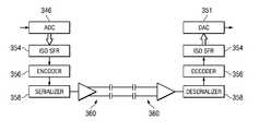
- the analog peripherals 340include an analog-to-digital converter 346 for receiving analog input signals from an analog multiplexer 348 interfaced to the plurality of input pins on the MCU 302 .
- the analog multiplexer 348allows the multiple outputs to be sensed through the pins 322 such that the analog-to-digital converter 346 can be interfaced to various sensors, such as a temperature sensor 342 .
- the operation of the multiplexer 348may also be controlled by an ADC auto scan function 345 .
- the output of the analog-to-digital converter 346may be provided to a number of SFR registers 352 . Responsive to information stored in the analog SFR registers 352 , an interrupt may be generated to download the stored information to an isolator SFR register 354 .
- the isolator SFR register 354generates an interrupt when it contains a byte of data to be transmitted. Once the interrupt is generated, the data within the ISO SFR register 354 is downloaded in parallel to encoder/decoder circuitry 356 .
- the encoder/decoder circuitry 356comprises a Manchester encoder for encoding/decoding information transmitted over the voltage isolation link and information received on the voltage isolation link. The operation of the Manchester encoder 356 will be more fully described herein below. It will, of course, be realized by those skilled in the art that other types of encoding/decoding circuitries may be utilized for the transmission of information across the voltage isolation link.
- serializer/deserializer circuit 358receives information from the encoder/decoder circuit 356 in parallel format and outputs it to the single channel bidirectional capacitive isolator circuit 360 in a serial format. In the receive mode of operation, the serializer/deserializer 358 receives serial data from the isolator circuit 360 and outputs it in parallel format to the encoder/decoder circuit 356 for decoding thereby in parallel format.
- the single channel bidirectional capacitive isolator 360is of the type described in U.S. patent application Ser. No. 12/060,049 entitled “CAPACITIVE ISOLATOR,” filed on Mar. 31, 2008, which is incorporated herein by reference. This will be more fully described herein below.
- Each of the serializer/deserializer circuit 358 and the capacitive isolator 360are clocked using a much higher clock rate than that utilized to clock the CPU, this generated with the use of a 16 ⁇ PLL clock multiplier circuit 362 .
- the 16 ⁇ PLL clock multiplier 362receives the clock signal from the multiplexer 311 which in the standard operating mode would comprise the 25 MHz oscillator signal.
- Analog datais provided to the analog-to-digital converter 346 within an MCU 102 which samples the analog input at a predefined sampling rate and generates a digital value therefore.
- This digital wordis stored within the isolator SFR register 354 .
- the data stored within the isolator SFR register 354causes the register 354 to generate an interrupt to the processing core 302 which will instruct the isolator SFR register 354 to download its presently stored sample into the encoder 356 .
- the encoder 356performs Manchester encoding or some other type of applicable encoding process to generate a parallel output stream of encoded data that is input to the serializer 358 .
- the serializer 358receives the encoded data in parallel and outputs the received data to the voltage isolation circuitry of the associated MCU 102 in serial format.
- the datais transmitted from the voltage isolation circuit 360 of one integrated microcontroller circuit to the voltage isolation circuit 360 of a receiving microcontroller circuit a single bit at a time and at a substantially higher bit rate that the sample rate.
- the received datais provided to a deserializer circuit 358 at the receiving microcontroller integrated circuit and the serialized data is converted from a serial format to a parallel format that is output to the decoder circuit 356 .
- the decoder circuitdecodes the information within the received data that has been Manchester encoded to provide the digital data that was originally encoded by the encoder 356 . (With Manchester encoding, the clock is recovered from the data.) This decoded information is output in parallel to the ISO SFR register 354 and stored therein until an interrupt generated by the SFR 354 enables the data to be processed by a digital-to-analog converter 351 wherein the digital sample is converted back into an analog signal.
- the encoder/decoder circuit 356may use Manchester encoding for encoding the received data.
- the first wayis to actually transmit the data on a single line and the clock signal on a separate line.
- I 2 Cis referred to as I 2 C.
- RS232is referred to as RS232.
- Each of these two serial data protocolsrequires a separate clock line in order to transmit the data. With this separate clock line, of course, the recovery of data is trivial and also allows the data rate to be increased.
- the datais transferred across the voltage isolation boundary with no separate clock signal. Therefore, there must be a way for the receive side to extract the data and the timing information from the signal. Typically, there must be some type of clock on the receive side that generates a sample signal that has some knowledge of the period in time during which to sample the data line wherein the data is valid.
- One type of serial data protocolis Manchester-coded data which utilizes clock recovery. This requires some type of start bit to indicate that a frame of data, i.e., a byte, is being transmitted, after which the data is transmitted in such a manner that clock information can be recovered from the actual data stream. Once the byte of data is transmitted, a stop bit is then sent.
- Manchester-coded datais utilized.
- Manchester encoding/decodingis well known in the art. Since the data may result in the transmission of a byte of data that is, for example, “00111011,” there can be at least two adjacent logic “1” states.
- Manchester-coderepresents binary values by transitions rather than the level, as would be found in a non-return to zero (NRZ) scheme. The transition occurs at mid-bit, with a low-to-high transition used to represent a logic “0” and a high-to-low transition to represent a logic “1.” Depending on the data stream, there may be a transition at the cell boundary (beginning/end). A pattern of consecutive “1s” or “0s” results in a transition on the cell boundary.
- Manchester-codingthere must be some type of synchronization on the receive side.
- center samplingoccurs at points 1 ⁇ 4 and 3 ⁇ 4 through the cell, since transitions occur always at mid-bit and sometimes on the cell boundaries.
- the receiver in a Manchester decoderdoes the clock recovery. Since Manchester encoding has transitions at least once each data cell, the receiver has known references to which it can resynchronize at each bit.
- the receiving circuitry in a Manchester decodercan use a digital phase lock loop or a counter algorithm. Digital phase locked loops are most often used in networks with a ring topology while counter algorithm are common in point-to-point links.
- An example of a counter algorithm which utilizes a 16 ⁇ clockrequires for the first step after receiving the initial transmission of the Manchester data to count the 16 ⁇ clock to four and then sample. The count of four is known as the n count. At this time, the n count is 1 ⁇ 4 through the data cell. Thereafter, the counter is reset to “0” and counting with the 16 ⁇ clock is begun with an n count of 8, followed by a sample. If there is a transition on the Manchester data, the counter is reset and this sequence is repeated.
- Manchester-codingWhen initialized correctly to the Manchester data, this algorithm causes the counter to use an n count equal to four when consecutive “1s” or “0s” are transmitted and an n count equal to 8 when alternating “1s” and “0s.”
- Manchester-codingsynchronizes on a bit basis.
- the result of utilizing Manchester-coding techniquesis that there is no DC component and it is well suited to be transformed or AC coupled.
- Manchester-codingrequires the modulation at a rate twice that of NRZ.
- a start bit at the beginning of a framecan utilize a sequence of a signal start bit, the eight data bits (for an eight input multiplexed system), an optional parity bit and one or more stop bits.
- Thisrequires the receive side to be set up to recognize the beginning of a frame with a start bit which could be a sample of a sequence of logic “1s” or a single bit.
- the stop bitcould be a single bit or a sequence of bits wherein, when the output goes low, this indicates the end of transmission of a particular frame. This will be described in more detail below.
- FIG. 5 athere is illustrated a more detailed diagrammatic view of the sampling and Manchester encoding operation.
- the illustration in FIG. 5 aillustrates the conversion of an analog signal 501 into a 4-bit data signal but in the preferred embodiment, the analog signal would be sampled using an 8-bit sample.
- the 4-bit sampleis merely used for purposes of simplifying the description and illustration, but any bit resolution could be used.
- Each samplewill create a 4-bit data word that is transmitted from the analog-to-digital converter 346 to the isolation SFR register 354 for each sample.
- a first sample 530there will be created a first sample 530 .
- the ADC conversion processcreates a sample output word of “1000” which constitutes the sampled data at that point in time.
- a second sampleis made resulting in a sample word “1110.”
- a sample word of “1110”is generated.
- the sample word createdis “1101.”
- the sample word of “1101”is created. This sampling is continuous across the received analog signal by the analog-to-digital converter 346 .
- the data wordis loaded into the isolation SFR register 354 for encoding and serializing for transmission across the isolation barrier. This is facilitated, as described herein above, with Manchester encoding. This is illustrated in detail at the bottom of FIG. 5 a .
- the start bitswill be raised high at a transition 540 and will be maintained high for one full cycle of the data clock.
- the data clock for Manchester encodingis twice that for NRZ, as there must be a transition at the mid point.
- the synchronizer on the opposite sidei.e., the receive side, will recognize the transition 540 and the lack of a transition at the mid point, keeping in mind that data clocks are synchronized.
- the first data bitwhich is a logic “1”
- the next two bitsare a logic “1”
- the next logic bitis a logic “0” which will result in a positive transition 548 at the mid point thereof.
- the stop bitis arrived at, it will be held high for a full clock cycle of the data clock. Thereafter, there will be a logic low during the entire clock cycle, represented by the reference numeral 550 . This will then be followed by a positive transition 552 for the start bit of the next word associated with the sample 536 . This will continue on in that sequence.
- the clock signals used for generation of the data that is transmitted across the capacitive isolation link of the microcontroller unitoperate according to the 25 MHz internal oscillation clock associated therewith. This is illustrated generally at 602 .
- the operation of the encoder/decoder 356 and the serializer/deserializer 358are according to the 16 ⁇ PLL clock multiplier circuit 362 that provides timing for these circuitries. Thus, these circuits operate according to a 400 MHz clock signal as indicated generally at 604 .
- the data that is transmitted across the capacitive isolation linkis transmitted according to a 400 MHz clock as indicated generally at 606 such that the serially transmitted data is not delayed too far behind the parallel bits that are being sampled according to the 25 MHz clock.
- the capacitive isolation circuitry used for transmitting the information in a voltage isolated fashionis more particularly illustrated in FIG. 7 .
- the capacitive isolation link 700consists of transmitter circuitry 702 and receiver circuitry 704 (a differential receiver).
- the transmitter circuitry 702consists of a pair of NAND gates 705 (a differential driver) and 706 having first inputs connected to receive the data to be transmitted over the capacitive isolation link and a second input connected to receive an RF carrier signal (16 Hz).
- RF carrier signalapplied to NAND gate 706 first goes through a phase shifter 703 which phase shifts the RF carrier 180 degrees.
- each of the NAND gates 705 and 706are connected to the inputs of inverters 708 and 710 respectively.
- the output of each of the inverters 708 and 710are connected to nodes 712 and 714 , respectively.
- An inverter 716has its input connected to node 714 and its output connected to node 712 .
- a second inverter 718has its input connected to node 712 and its output connected to node 714 .
- a first transmission gate 720has its input connected to node 712 and its output connected to node 722 .
- a second transmission gate 724has its input connected to node 714 and its output connected to node 726 .
- a resistor 728is connected between node 722 and node 730 .
- a second resistor 732is connected between node 726 and node 734 .
- Node 730is connected with a first isolation capacitor 736 and node 734 is connected with a second isolation capacitor 738 .
- the transmission gates 720 and 724are enabled when the differential driver circuit is transmitting data over the capacitive isolation link.
- the RF transmission signalis continually applied to one input of NAND gates 705 and 706 .
- When a 1-bit is also transmitted on the other input of the NAND gates 705 and 706the RF signal is transmitted over each of the transmission lines of the capacitive isolation link with the RF signal on the TX ⁇ line being 180 degrees out of phase with the RF signal on the TX+ line.
- a 0-bitis applied to the inputs of NAND gates 705 and 706 , no RF signal is transmitted over the capacitive link.
- the capacitors 736 and 738are connected across an isolation barrier 740 .
- the isolation barriermay be between different chips or different dies in a single package.
- Capacitors 736 and 738connect across the isolation barriers with isolation capacitor 742 and 744 , respectively.
- Capacitors 742 and 744are associated with the receiver circuitry 704 .
- Capacitor 742connects with the receiver circuitry at node 746 .
- Capacitor 744connects with the receiver circuitry at node 748 .
- the receiver circuitry 704comprises a differential receiver consisting of a bias and transient common mode clamp circuitry 750 for preventing the receiver node from floating and limiting the input common mode voltage to the receiver from exceeding the operating range of the receiver protecting a receiver amplifier 752 .
- the receiver amplifier 752detects a received signal.
- the bias and transient clamp circuitry 750comprises a P-channel transistor 754 having its source/drain path connected between V DD and node 746 .
- An N-channel transistor 756has its drain/source path connected between node 746 and node 758 .
- a P-channel transistor 760has its source/drain path connected between node 758 and ground.
- a resistor 762is connected between node 746 and node 764 .
- the gates of each of transistors 754 and 756are connected to node 764 .
- the gate of transistor 760connects with the gate of a transistor 766 which is connected to a circuit (not shown) providing a bias voltage BIAS 1 .
- Transistor 768is a P-channel transistor having its source/drain path connected between V DD and node 748 .
- An N-channel transistor 770has its drain/source path connected between node 748 and node 772 .
- the P-channel transistor 766having its gate connected with transistor 760 has its source/drain path connected between node 772 and ground.
- the gates of each of transistors 770 and 756are connected to node 764 .
- a resistor 774is connected between node 748 and node 764 .
- the bias and common clamp circuitry 750clamps receive input nodes to keep them from floating when no RF signal is applied and clamps the input voltage to the receiver.
- the receiver amplifier 752interconnects with the isolation capacitors at nodes 746 and 748 respectively. These nodes are connected with the gates of N-channel transistors 776 and 778 .
- Transistor 776is connected between nodes 780 and 781 .
- Transistor 778has its drain/source path connected between node 782 and node 781 .
- a transistor 783has its drain/source path connected between node 781 and ground. The gate of transistor 783 is connected to bias circuitry (not shown) providing a bias voltage BIAS 2 .
- a P-channel transistor 784has its source/drain path connected between V DD and node 780 .
- a transistor 785has its source/drain path connected between V DD and node 782 .
- a resistor 786is connected between the gate of transistor 784 and node 780 .
- a resistor 788is connected between the gate of transistor 785 and node 782 .
- the receive signals over the capacitive linkcan be detected at either of nodes 780 and 782 and the received signals are offset from each other by 180 degrees.
- directional controlcan be provided by either a bonding option to connect the tx_en to a logic “high” or “low” to determine direction or have it determined by the respective MCU.
- FIGS. 8 , 8 a and 9there are illustrated the waveforms and data provided at the transmission side ( FIGS. 8 and 8 a ) of a capacitive isolation link and the receive side ( FIG. 9 ) of a capacitive isolation link.
- the datais either transmitted as a one bit (high) or zero bit (low).
- a one bit pulseis indicated at 802 and 804 .
- a zero bit pulseis indicated at 808 and 810 .
- the transmit data provided to the capacitive linkis illustrated by the waveform 812 .
- the transmit data waveformrepresents the 1 GHz RF carrier signal.
- the RF carrier signalcan be of any frequency. The use of different frequencies enables the provision of lower power circuitries with lower frequencies.
- a logical “0” bitis being transmitted, the signal is virtually zero at the transmit data output. Thus, whether a logical “1” bit or a logical “0” bit is transmitted is indicated either by the presence or absence of the RF carrier signal.
- FIG. 8 aillustrates the manner in which the wave form 812 is transmitted on each of the transmission lines of the capacitive link.
- a first RF signal 820comprises the information transmitted on the TX+ line of the capacitive link from the differential driver.
- the wave form 822comprises the inverted format of the RF signal on the TX ⁇ line that is 180 degrees out of phase with signal 820 .
- FIG. 9illustrates the waveforms associated with the receiver 704 .
- the received data for the logic “1” bitis represented at points 902 and 904 and indicates the two 1 GHz RF carrier pulses transmitted from the transmitter 702 of the capacitive isolation link.
- the received pulsesare amplified by the amplifier 752 such that the pulses are represented by the amplified waveform pulses 906 , 910 , 912 and 908 .
- the detector data outputrises to V DD at points 910 and 912 when no RF carrier signal is detected indicating a logical “0.”
- the output of the detector 704begins to vary at points 906 and 908 indicating a logical “1,” this being the result of an increase in the NMOS current in transistors 776 and 778 .
- Capacitor 1102represents a 165 fF capacitor connected between node 1104 and ground.
- Capacitor 1106represents a 53 fF capacitor connected between node 1108 and ground.
- the connection between node 1104 and node 1108is represented by an 88 fF capacitor 1110 .
- the RF isolation circuitmay provide 5,000 volts of isolation between a first MCU and a second MCU. While the voltage between the input terminals of the first MCU will be zero volts and the voltage between the input terminals of the second MCU will also be zero volts, the total voltage difference between the two MCUs may be 5,000 volts with a 2,500 voltage difference across each of the capacitors associated with the interfaces to the capacitive isolation circuit on each MCU. (Note that this requires each capacitor to only provide a capacitor dielectric with a breakdown voltage in excess of 2,500 Volts.)
- the RF isolation linkconsists of transmitter circuitry 1202 and receiver circuitry 1204 .
- the transmitter circuitry 1202consists of a NAND gate 1208 having a first input connected to receive the data to be transmitted over the RF isolation link and a second input connected to receive the RF carrier signal.
- the RF carrierin this embodiment comprises a 2 GHz signal.
- the data input to the first input of the NAND gate 1208consists of either a logical “1” or “0” which will selectively gate the RF carrier signal to the output of NAND gate 1208 in the presence of a logical “1.” This causes the output 1209 of the NAND gate 1208 to either provide the RF carrier signal when the data bit is “1” or not provide the RF signal when the data bit is “0.”
- the output of the NAND gate 1209is connected to the gate of a p-channel transistor 1210 .
- the drain-source path of the p-channel resistor 1210is connected between VDD and ground through a resistor 1212 and a first transformer 1214 .
- the transformer 1214electromagnetically couples the RF carrier signal to transformer 1218 via lines 1216 .
- Each of the transformers 1214 and 1218are associated with a particular MCU on opposite sides of interface 1220 .
- the present disclosed deviceintegrates the RF isolation link onto the MCUs.
- TX/RX enablewith respect to the gate 1208 to allow for directional programming thereof.
- the receiver circuitry 1204receives the signal which has been electromagnetically coupled via transformer 1214 onto the transmission lines 1216 to transformer 1218 .
- the receiver circuit 1204consists of an amplifier 1205 and a detector 1206 .
- the amplifier 1205provides two stages of amplification consisting of a first amplification stage including a capacitor 1222 in series with an amplifier 1224 and a feedback resistor 1226 .
- the second amplifier stageis similar to the first amplifier stage and includes a capacitor 1228 in series with an amplifier 1230 and a feedback resistor 1232 . These two stages amplify the received signal from the transformer 1218 .
- the detector 1206detects the presence or absence of the RF carrier signal within the amplified received signal to determine the data being transmitted from the first MCU.
- the amplified signal from the amplifier 1205is first filtered by a capacitor 1234 .
- N-channel transistor 1236has the gate thereof connected to capacitor 1234 and has the source-drain path thereof connected to one side of a current mirror comprised of p-channel transistors 1238 and 1240 .
- the source-drain path of transistor 1238is connected between VDD and node 1242 , the gate thereof connected to the gate of transistor 1240 .
- the source-drain path of transistor 1240is connected between VDD and a node 1243 , the gate thereof connected to node 1243 to provide a diode connected configuration.
- the output of the detector 1206is provided from node 1242 at which the source-drain path of the n-channel transistor 1236 is connected to the p-channel transistor 1238 of the current mirror.
- a bias networkis provided by n-channel transistors 1244 and 1246 which have the source-drain paths thereof connected between node 1243 and ground and the gates thereof connected to a node 1245 through a resistor 1248 , with a capacitor 1250 connected between node 1245 and ground. Biasing is also provided by resistor 1252 connected between node 1245 and the gate of transistor 1236 , a diode connected p-channel transistor 1254 connected between node 1245 and ground and a current source 1256 for driving node 1245 .
- the Data Out from node 1242 of the detector circuit 1206When no RF signal is detected by the receiver, the Data Out from node 1242 of the detector circuit 1206 will be equal to VDD since the PMOS current is greater than 1.33 times the NMOS current and a logical “0” is detected. In the presence of the RF signal, the Data Out from node 1242 will vary in response to the variation of the detected RF carrier signal and a logical “1” is detected.
- the detector 1206outputs a low voltage when RF is present and a high voltage when RF is absent relying on the nonlinear (square root) behavior of the MOS device directed by the alternating current.
- FIG. 13there is illustrated a model for the transformers ( 1214 , 1218 ) illustrated in FIG. 12 .
- the input of the transformerconsists of nodes 1302 and 1300 .
- Node 1302is connected to ground through capacitor 1304 and resistor 1306 .
- Node 1300is connected to ground through capacitor 1316 and resistor 1318 .
- Node 1302interconnects with node 1300 via a parallel connection of capacitor 1308 in series with resistor 1310 and inductor 1312 in series with resistor 1314 .
- the output of the transformerconsists of nodes 1322 and 1324 .
- Node 1322is connected to ground through capacitor 1326 and resistor 1328 .
- Node 1324is connected to ground through capacitor 1330 and resistor 1332 .
- Node 1322interconnects with node 1324 via a parallel connection of capacitor 1334 in series with resistor 1336 and inductor 1338 in series with resistor 1340 .
- Nodes 1302 and 1322are interconnected via a capacitor 1342 with a value of approximately 125 fF.
- Nodes 1300 and 1324are interconnected via a capacitor 1344 with a value of approximately 125 fF.
- the RF isolation circuitmay provide 5,000 volts of isolation between a first MCU and a second MCU. While the voltage between the input terminals of the first MCU will be zero volts and the voltage between the input terminals of the second MCU will also be zero volts, the total voltage difference between the two MCUs may be 5,000 volts with a 2,500 volt difference across each of the transformers 1214 , 1218 associated with the interfaces to the RF isolation circuit on each MCU.
- an I 2 C protocolmay be used to communicate information from one microcontroller unit 1502 to a second microcontroller unit 1504 wherein the I 2 C protocol is maintained on each side of the voltage isolation link.
- the pair of MCUsmay be used as a protocol converter.
- Input to the first MCU 1502is data according to the I 2 C protocol (by way of illustration, understanding that any data protocol could be utilized). That information is transmitted across the voltage isolation link between the two MCUs and at the second MCU 1504 , the data is output in the SPI interface format (different protocol than that on the other side of the isolation boundary).
- the conversion from one protocol to the othermay be according to any particular protocol and the use of the I 2 C and SPI protocols is merely by way of example.
- FIG. 15 cillustrates the manner in which the microcontroller units 1502 may be used to provide a conversion from a digital signal to an analog signal or vice versa across the voltage isolation barrier.
- a digital signalis input or output from an MCU on one side of the voltage isolation barrier and the analog is input or output from the MCU at the microcontroller unit 1502 on the other side of the voltage isolation barrier.
- digital-to-digital or analog-to-analog conversionsmay be performed as shown in FIGS. 15 d and 15 e .
- FIG. 15 d and 15 eillustrates the manner in which the microcontroller units 1502 may be used to provide a conversion from a digital signal to an analog signal or vice versa across the voltage isolation barrier.
- FIG. 15 dillustrates how a digital signal is transmitted across the voltage isolation barrier from a first microcontroller unit 1502 to the second microcontroller unit 1502 .
- an analog signalmay be provided on one side of a voltage isolation barrier at a microcontroller unit 1502 and output on the opposite side of the barrier at a second microcontroller unit 1502 as the same analog signal.
- the analog or digital signalsmay be provided on opposite sides of the voltage isolation barriers according to different protocols as described previously with respect to FIG. 15 b .
- the combination of the microcontroller unit and voltage isolation circuitries implemented within a single integrated microcontroller unitprovides circuit designers with a great deal of flexibility for transmitting signals in varying formats across high voltage isolation links.
- FIG. 16there is illustrated a diagrammatic view of the embodiment wherein two separate die are disposed in a common package with a galvanically isolated boundary disposed therebetween with the capacitive (or inductive) isolator structure providing the data transfer connection therebetween.
- lead frames 1602 and 1604There are provided two lead frames 1602 and 1604 .
- Each of the lead frames 1602 and 1604includes a die mounting pad 1606 and 1608 , respectively.
- Die mounting pad 1606has two ground leads 1610 and 1612 associated therewith that extend from a package boundary 1614 .
- the die mounting pad of 1608has two ground leads 1616 and 1618 , respectively associated therewith.
- die 1620 and 1622Mounted on the surface of the two die mounting pads 1606 and 1608 are die 1620 and 1622 , respectively. Each of these die 1620 and 1622 have associated therewith the MCU/isolator combination described hereinabove.
- the two separate die mounting pads 1606 and 1608provide a completely separate DC connection such that the two die 1620 and 1622 are galvanically isolated.
- the die mounting body 1606Associated with the die mounting body 1606 are a plurality of leads 1624 and, similarly, the die mounting body 1608 has associated therewith a plurality of leads 1626 .
- the die mounting pads 1608 and 1606are each provided for mounting the chip thereon. Typically, the bottom surface of the chip will be associated with a ground connection.
- bonding pads 1638which correspond to the upper plates of the capacitors on the die 1620 associated with the isolator function. Of course, this also could represent the top coil in an inductor connection, as described hereinabove.
- pads 1640On the die 1622 , there are provided two corresponding pads 1640 .
- bond wires 1642connecting the pads 1638 to the pads 1640 . This provides the isolation function.
- MCU/isolator functionalityis described as being contained on a common die 1620 or 1622 , it should be understood that multiple chips could be mounted onto the respective die mounting body 1606 or 1608 . This is not uncommon in a packaged integrated circuit. It could be that the processor functionality is contained on a separate MCU chip and a separate isolator chip would be provided. For example, it might be that a separate integrated circuit could have been utilized for just the capacitors themselves, to take advantage of a separate high voltage process for the capacitors to provide a significantly higher breakdown voltage.
- serial data formatIn order to transmit data across the isolation boundary, the data must be converted to a serial data format.
- one serial data formatthat has been proposed is that utilizing a Manchester coded data string. This is asynchronous transmission, which requires clock recovery at the opposite end, i.e., the receiving end.
- a “two-wire” systemcould be utilized wherein a first path is provided for a clock signal and a second path is provided for the data. This, of course, would require two isolation circuits and four capacitors (or four inductors).
- Parallel datacould be transmitted in parallel, which would require, for example, eight data paths for transmission/reception for an 8-bit wide bus.
- the disclosed embodiment hereinaboveutilizes a parallel-to-serial conversion operation wherein parallel data is converted to serial data and then transmitted across the boundary. Since the parallel data is generated and transmitted at substantially the clock rate of the processor, the conversion to serial data and transmission thereof across the isolation boundary must be faster, thus requiring the higher frequency serial clock. Of course, if only serial data formats were to be transmitted, i.e., SPI formatted data or I 2 C formatted data, then the higher frequency clock would not be necessary. Parallel data could not then be accommodated over a single data path.
- both processors on either side of the isolation boundarywould have to have common programs wherein the data were transmitted at one particular rate, i.e., the parallel data were first loaded into the SFR 354 and then processed until it was received at the SFR 354 on the opposite side generating an interrupt. The data would then be processed on the receiving side in such a manner that the SFR 354 were cleared allowing the next byte of data to be received therein.
- thisis an operation where the timing on both sides of the isolation boundary would have to be coordinated such that the overall operation functioned with an elastic buffer configuration.
- serial datais to be transmitted
- datawould be received in a serial format, for example, the UART block 326 .
- Interfaced to the exterior world on one side of the isolation boundarywould be the UART functionality.
- This UART 326would interface with select ones of the port pins 322 .
- the datawould be received as serial data in accordance with the UART protocol, converted to parallel data on the SFR bus 320 and then processed by loading that information into the ISO SFR 354 .
- the isolation boundaryOn the opposite side the isolation boundary, on the receive side thereof, the data that is being received across the isolation boundary could be converted back to a UART format and transmitted.
- the datacould be received by the ADC 346 at the sampling rate thereof, converted to a parallel data and loaded into the ISO SFR 354 at the sampling rate. All that is required is that the isolation circuitry, i.e., the encoder/decoder 356 and the serializer/deserializer block 358 operate at a sufficiently high enough frequency to convert the data from parallel data to serial data, transmitted across the isolation boundary and then be ready for the next byte of data that is sampled by the ADC 346 .
- the isolation circuitryi.e., the encoder/decoder 356 and the serializer/deserializer block 358 operate at a sufficiently high enough frequency to convert the data from parallel data to serial data, transmitted across the isolation boundary and then be ready for the next byte of data that is sampled by the ADC 346 .
- datacould be received on one side in a UART format and transmitted out in an SMBus format, which is basically an I 2 C protocol, with the block 332 . All that is required is that the particular MCU to be programmed on either side of the isolation boundary and that the programs on both sides of the isolation boundary be coordinated. To the user, however, these are transparent, i.e., if data is transmitted into the chip on one side, it shows up at the other side as if transmitted directly therethrough. For example, if parallel data were input to one side of the isolation boundary, one of the port pins would be basically a toggle pin that would clock the data through.
- FIG. 17there is illustrated a diagrammatic view illustrating two sides of an isolation boundary 1702 , with an MCU 1704 disposed on one side thereof and MCU 1706 disposed on the other side thereof.
- the productcould be programmed restricted to a single direction, i.e., on one side, the transmitter is enabled such that it is always in the transmit mode and on the other side, the transmitter is disabled. This would be a unidirectional operation.
- the chipis manufactured and packaged for this operation, all that would be required is to connect the enable pin to a high voltage or low voltage, a bonding option.
- bidirectional transferis required, then there must be a provision to enable or disable the transmit operation. This is the embodiment disclosed in FIG. 17 .
- the transmit enable portion of the transmitteris illustrated by a function block 1708 on both sides of the isolation boundary 1702 . It should be understood that both sides of the isolation boundary 1702 will have similarly labeled parts.
- a transmitter 1710on each side that provides an input to the transmit enable block 1708 .
- the transmitter 1710has an encoder/serializer associated therewith.
- Each side of the isolation boundary 1702has a control SFR 1712 that will contain bits that will configure and control the operation. Generally, a bit can be set by the respective MCU 1704 and 1706 to configure the operation as transmit or receive.
- the output of the transmit enabledrives one side of two capacitors 1714 on one side of the isolation boundary 1702 associated with the MCU 1704 and the transmit enable block 1708 drives one side of two capacitors 1718 on the side of the isolation boundary 1702 associated with the MCU 1706 .
- the top plates of the capacitors 1714 and 1718are connected together, as described hereinabove. Again, as noted hereinabove, these could be inductive and not necessarily capacitive.
- a receiver 1720is provided on both sides of the isolation boundary and connected to the bottom plates of capacitors 1714 and 1718 , respectively.
- Each of the receivers 1720will have the output thereof passed through the encoder/decoder/serializer/deserializer block 1722 to provide data to the ISO SFR 354 . This is then input to the MCU 1704 .
- the respective receiverwill generate the data and store it in the SFR 354 and generate an interrupt after storage thereof.
- the MCU 1704 or the MCU 1706will be aware of when data is transmitted. Thus, whenever it is desirable to transmit data, it will be necessary first to determine if data is being received.
- the interruptwill cause the bus to be indicated as being seized by the opposite side, i.e., the other side of the isolation boundary 1702 has seized the bus or data communication path.
- the side having received datawill determine if it has to wait to transmit data.
- MCU 1704 or 1706examines its interrupt status to determine if data has been received within a certain amount of time. If not, then that means that the data communication path is available and the transmitter can be enabled and then data transferred.
- FIG. 18there is illustrated an alternate embodiment wherein a separate transmit path and a separate receive path can be provided.
- a second set of capacitors 1810 on the MCU 1704 side of the isolation boundary 1702 and a pair of capacitors 1812 on the MCU 1706 of the isolation boundarywould provide for transmission from the MCU 1704 to the MCU 1706 .
- Thiswould have a transmitter 1816 on the MCU 1704 side of the isolation boundary and a receiver 1818 on the MCU 1706 side of the isolation boundary 1702 .
- the transmitter 1816 and the transmitter 1806have encoder/serializer blocks associated therewith.
- the MCU 1704would transmit data through the transmitter 1816 , capacitors 1810 and 1812 and receiver 1818 for encoding/decoding and serializing with a block 1824 for loading into the ISO SFR 354 on the MCU 1706 side of the isolation boundary 1702 .
- the MCU 1704would receive data through the receiver 1808 and an encoder/decoder/serializer on the MCU 1704 side of the isolation boundary 1702 . This would be stored in the ISO SFR 354 associated therewith.
- the analog multiplexer 348is utilized to scan the analog inputs in other auto scan mode or under the control of the 8051 core 302 .
- the auto scan featureis described in U.S. Pat. No. 7,142,140, issued Nov. 28, 2006, which is incorporated herein by reference in its entirety.
- the MCU 104is described herein.
- the analog inputsare scanned and input to the ADC 346 .
- the ADC 346is sampled at a 16 MHz rate.
- the datais then sequentially input to one of the SFRs 352 .
- the SFRs 352can incorporate an interrupt feature wherein there is a limit function to provide an over/under window for comparison therewith. If the analog voltage goes outside of that window (or, conversely, within the window), then an interrupt is generated.
- the 8051 core 302 associated with that side of the isolation barrier 202will service that interrupt.
- the contents of the SFR 352 generating the interruptwill be transferred to the isolator SFR 354 and, at that time, the isolator circuitry, comprised of the encoder/decoder 356 , serial/deserializer 358 and capacitive isolator 360 , will be utilized to transfer the data across the isolation barrier 202 .
- This isolation functionis illustrated by a block 1902 for simplicity.
- the corresponding isolation block 1902will decode the information and store it in the isolator SFR 354 associated with that side.
- an interruptis generated by the decoding circuitry indicating that a byte has been decoded and has been transferred to the SFR 354 .
- the 8051 core 302 on that side of the isolation barrierwill service the interrupt and then extract the data from the SFR 354 for processing thereof.
- a command structurecould be utilized. This is illustrated in FIG. 19 a .
- this type of structurewhat occurs is that a sequence of known bytes of data are transferred across the isolation barrier to the 8051 core 302 .
- thiscan be a command structure. This would be comprised of a header or start field, a command field and a stop or end field.
- the header fieldcould be as simple as one or two bytes of data with alternating “1's” “0's” or some other known sequence.
- the 8051 core 302will recognize this as a synchronizing section indicating that, after three or four bytes (it could even be one byte), the next byte or sequence of bytes, a predetermined number, would be received indicating the command.
- the commandcould be that the next data to be received will be analog data that is being sensed from a defined input of the multiplexer 348 . It is necessary to keep in mind that both sides of the isolation barrier are programmed for a particular application, although a more sophisticated command language could be utilized to facilitate multiple applications. Once the command has been interpreted, this will be followed by an end field or stop field. This again, is a sequence of bytes of known values. The next byte of data or bytes of data would be the contents of the SFR 352 that generated the interrupt.
- the 8051 core 302in accordance with instructions associated therewith and executed thereon would go through and scan the various inputs by controlling the multiplexer 348 to select any one input.
- one of the inputscould be the temperature, and the program could require temperature to be sensed at periodic intervals. When this temperature is sensed, it is then transferred to the 8051 core 302 on the opposite side of the isolation barrier with an indication thereof. This just requires the command structure in FIG. 19 a to be followed.
- the systemis configured to transmit a single one of the sensed inputs in the analog domain as a received analog value and transmitted across the isolation barrier 202 to the SFR 354 for output as an analog value in real time. When received, it will immediately be transmitted out of the DAC 351 to an analog output 1906 . Thus, what would occur would be a straight pass through of an analog value from one side to the other. It should be remembered, however, that there will be some latency associated with the transfer, but latency will be relatively small.
- the MCUs on either side of the galvanic isolation barriercan be programmed such a single bit received on one GPIO pin on one side can be transmitted across the isolation or galvanic barrier as a part of a parallel word—the only part. Each bit is stored in the parallel word stored in the SFR 354 as the LSB. When decoded, the MCU on the receiving side extracts the LSB and outputs it to a GPIO pin on the receiving side.
Landscapes
- Engineering & Computer Science (AREA)
- Computer Hardware Design (AREA)
- Microelectronics & Electronic Packaging (AREA)
- Power Engineering (AREA)
- Physics & Mathematics (AREA)
- Condensed Matter Physics & Semiconductors (AREA)
- General Physics & Mathematics (AREA)
- Dc Digital Transmission (AREA)
Abstract
Description
Claims (29)
Priority Applications (1)
| Application Number | Priority Date | Filing Date | Title |
|---|---|---|---|
| US12/164,998US7737871B2 (en) | 2004-06-03 | 2008-06-30 | MCU with integrated voltage isolator to provide a galvanic isolation between input and output |
Applications Claiming Priority (8)
| Application Number | Priority Date | Filing Date | Title |
|---|---|---|---|
| US10/860,519US7447492B2 (en) | 2004-06-03 | 2004-06-03 | On chip transformer isolator |
| US10/860,399US7421028B2 (en) | 2004-06-03 | 2004-06-03 | Transformer isolator for digital power supply |
| US11/020,977US7376212B2 (en) | 2004-06-03 | 2004-12-22 | RF isolator with differential input/output |
| US11/064,413US7460604B2 (en) | 2004-06-03 | 2005-02-23 | RF isolator for isolating voltage sensing and gate drivers |
| US11/089,348US7302247B2 (en) | 2004-06-03 | 2005-03-24 | Spread spectrum isolator |
| US11/772,178US8049573B2 (en) | 2004-06-03 | 2007-06-30 | Bidirectional multiplexed RF isolator |
| US12/060,049US8169108B2 (en) | 2004-06-03 | 2008-03-31 | Capacitive isolator |
| US12/164,998US7737871B2 (en) | 2004-06-03 | 2008-06-30 | MCU with integrated voltage isolator to provide a galvanic isolation between input and output |
Related Parent Applications (1)
| Application Number | Title | Priority Date | Filing Date |
|---|---|---|---|
| US12/060,049Continuation-In-PartUS8169108B2 (en) | 2004-06-03 | 2008-03-31 | Capacitive isolator |
Publications (2)
| Publication Number | Publication Date |
|---|---|
| US20090027243A1 US20090027243A1 (en) | 2009-01-29 |
| US7737871B2true US7737871B2 (en) | 2010-06-15 |
Family
ID=40294819
Family Applications (1)
| Application Number | Title | Priority Date | Filing Date |
|---|---|---|---|
| US12/164,998Expired - LifetimeUS7737871B2 (en) | 2004-06-03 | 2008-06-30 | MCU with integrated voltage isolator to provide a galvanic isolation between input and output |
Country Status (1)
| Country | Link |
|---|---|
| US (1) | US7737871B2 (en) |
Cited By (37)
| Publication number | Priority date | Publication date | Assignee | Title |
|---|---|---|---|---|
| US20080179963A1 (en)* | 2006-08-28 | 2008-07-31 | Avago Technologies Ecbu (Singapore) Pte. Ltd. | Galvanic Isolators and Coil Transducers |
| US20090010371A1 (en)* | 2006-01-03 | 2009-01-08 | Nxp B.V. | Serial data communication system and method |
| US20100148911A1 (en)* | 2007-05-10 | 2010-06-17 | Avago Technologies Ecbu Ip (Singapore) Pte. Ltd. | Miniature Transformers Adapted For Use In Galvanic Isolators And The like |
| US20100176660A1 (en)* | 2006-08-28 | 2010-07-15 | Avago Technologies General IP (Singpore) Pte. Ltd. | Galvanic isolator |
| US20100259909A1 (en)* | 2006-08-28 | 2010-10-14 | Avago Technologies Ecbu (Singapore) Pte. Ltd. | Widebody Coil Isolators |
| US20110006814A1 (en)* | 2009-07-02 | 2011-01-13 | Nxp B.V. | Power stage |
| US20110075449A1 (en)* | 2008-03-31 | 2011-03-31 | Avago Technologies Ecbu Ip (Singapore) Pte. Ltd. | Compact Power Transformer Components, Devices, Systems and Methods |
| US20110156812A1 (en)* | 2009-12-31 | 2011-06-30 | Avago Technologies Wireless Ip (Singapore) Pte. Ltd. | Multi-band, multi-mode rf transmit amplifier system with separate signal paths for linear and saturated operation |
| US8385043B2 (en) | 2006-08-28 | 2013-02-26 | Avago Technologies ECBU IP (Singapoare) Pte. Ltd. | Galvanic isolator |
| US20130057428A1 (en)* | 2010-03-08 | 2013-03-07 | Armin Himmelstoss | Radar sensor and method for controlling same to reduce the crosstalk of digital signals to the hf radar signal |
| US8497700B2 (en) | 2011-10-21 | 2013-07-30 | Samsung Electro-Mechanics | Systems and methods for propagating digital data across an isolation barrier |
| US8502584B1 (en) | 2012-03-30 | 2013-08-06 | Silicon Laboratories Inc | Capacitive isolation receiver circuitry |
| WO2013155565A1 (en)* | 2012-04-18 | 2013-10-24 | The Silanna Group Pty Ltd | Single-chip multi-domain galvanic isolation device and method |
| US8571093B1 (en) | 2012-04-24 | 2013-10-29 | Nxp B.V. | Communication interface for galvanic isolation |
| US8644365B2 (en)* | 2012-03-30 | 2014-02-04 | Silicon Laboratories Inc. | Providing voltage isolation on a single semiconductor die |
| US8680690B1 (en) | 2012-12-07 | 2014-03-25 | Nxp B.V. | Bond wire arrangement for efficient signal transmission |
| US8787502B2 (en) | 2012-04-24 | 2014-07-22 | Nxp B.V. | Capacitive isolated voltage domains |
| US20140233614A1 (en)* | 2013-02-20 | 2014-08-21 | Fairchild Semiconductor Corporation | Isolation communication technology using coupled oscillators/antennas |
| US8818265B2 (en) | 2012-04-24 | 2014-08-26 | Nxp B.V. | Interface for communication between voltage domains |
| US8829955B1 (en)* | 2013-03-14 | 2014-09-09 | Analog Devices, Inc. | Isolator-based transmission system with side isolator channel for refresh signals |
| US20140253227A1 (en)* | 2013-03-10 | 2014-09-11 | Microchip Technology Incorporated | Integrated High Voltage Isolation Using Low Value Capacitors |
| US20140300188A1 (en)* | 2013-04-03 | 2014-10-09 | Nep B.V. | Capacitive level shifter devices, methods and systems |
| US8867592B2 (en) | 2012-05-09 | 2014-10-21 | Nxp B.V. | Capacitive isolated voltage domains |
| US8896377B1 (en) | 2013-05-29 | 2014-11-25 | Nxp B.V. | Apparatus for common mode suppression |
| US20150071380A1 (en)* | 2013-09-09 | 2015-03-12 | Texas Instruments Incorporated | Method and circuitry for transmitting data |
| US9007141B2 (en) | 2012-05-23 | 2015-04-14 | Nxp B.V. | Interface for communication between voltage domains |
| US9065461B1 (en)* | 2015-01-15 | 2015-06-23 | Avago Technologies General Ip (Singapore) Pte. Ltd. | Coding and decoding isolation device and method thereof |
| US20150200162A1 (en)* | 2014-01-10 | 2015-07-16 | Fairchild Semiconductor Corporation | Isolation between semiconductor components |
| US9105391B2 (en) | 2006-08-28 | 2015-08-11 | Avago Technologies General Ip (Singapore) Pte. Ltd. | High voltage hold-off coil transducer |
| US9177925B2 (en) | 2013-04-18 | 2015-11-03 | Fairfchild Semiconductor Corporation | Apparatus related to an improved package including a semiconductor die |
| US9337253B2 (en) | 2013-03-09 | 2016-05-10 | Microchip Technology Incorporated | Method and apparatus for constructing an isolation capacitor in an integrated circuit |
| US9948193B2 (en) | 2016-06-10 | 2018-04-17 | Stmicroelectronics S.R.L. | Galvanically isolated DC-DC converter with bidirectional data transmission |
| US9978511B2 (en) | 2015-12-01 | 2018-05-22 | Stmicroelectronics S.R.L. | Galvanic isolation system, apparatus and method |
| US10193581B2 (en) | 2016-08-30 | 2019-01-29 | Stmicroelectronics S.R.L. | Galvanic isolation circuit, corresponding system and method |
| US10277278B2 (en) | 2014-09-24 | 2019-04-30 | Analog Devices, Inc. | Circuits and systems for multiplexed isolator communication |
| US10298408B2 (en) | 2015-09-09 | 2019-05-21 | Stmicroelectronics S.R.L. | Method of transmitting power and data across a galvanic isolation barrier, corresponding system and apparatus |
| US10930604B2 (en) | 2018-03-29 | 2021-02-23 | Semiconductor Components Industries, Llc | Ultra-thin multichip power devices |
Families Citing this family (15)
| Publication number | Priority date | Publication date | Assignee | Title |
|---|---|---|---|---|
| US8902016B2 (en)* | 2009-10-21 | 2014-12-02 | Stmicroelectronics S.R.L. | Signal transmission through LC resonant circuits |
| US8558344B2 (en) | 2011-09-06 | 2013-10-15 | Analog Devices, Inc. | Small size and fully integrated power converter with magnetics on chip |
| FR2984661B1 (en)* | 2011-12-19 | 2013-12-20 | Valeo Sys Controle Moteur Sas | METHOD OF COMMUNICATING BETWEEN AT LEAST ONE FIRST SYSTEM AND AT LEAST ONE SECOND SYSTEM THROUGH A FULL DUPLEX SYNCHRONOUS SERIAL LINK |
| US8786393B1 (en) | 2013-02-05 | 2014-07-22 | Analog Devices, Inc. | Step up or step down micro-transformer with tight magnetic coupling |
| US9293997B2 (en) | 2013-03-14 | 2016-03-22 | Analog Devices Global | Isolated error amplifier for isolated power supplies |
| JP6129659B2 (en)* | 2013-06-25 | 2017-05-17 | ルネサスエレクトロニクス株式会社 | Semiconductor device and manufacturing method thereof |
| KR102080453B1 (en)* | 2013-10-02 | 2020-02-24 | 현대모비스 주식회사 | Watchdog apparatus and method thereof |
| US9544027B2 (en)* | 2014-02-19 | 2017-01-10 | Texas Instruments Incorporated | Loop powered transmitter with a single tap data isolation transformer and unipolar voltage converters |
| US9816872B2 (en)* | 2014-06-09 | 2017-11-14 | Qualcomm Incorporated | Low power low cost temperature sensor |
| US9634646B1 (en)* | 2015-10-27 | 2017-04-25 | Analog Devices, Inc. | Mismatch calibration of capacitive differential isolator |
| US10554456B2 (en)* | 2017-08-23 | 2020-02-04 | Semiconductor Components Industries, Llc | Circuits and methods for bi-directional data communication over isolation channels |
| US10943855B2 (en)* | 2017-08-23 | 2021-03-09 | Semiconductor Components Industries, Llc | Electronic device packaging with galvanic isolation |
| US12200089B2 (en)* | 2020-02-05 | 2025-01-14 | Intel Corporation | Bi-directional buffer with circuit protection time synchronization |
| EP3975493A1 (en)* | 2020-09-25 | 2022-03-30 | STMicroelectronics S.r.l. | Communication method, corresponding system and device |
| US12212440B2 (en) | 2023-01-10 | 2025-01-28 | Navitas Semiconductor Limited | Systems and methods for signal isolation in power converters |
Citations (149)
| Publication number | Priority date | Publication date | Assignee | Title |
|---|---|---|---|---|
| US3058078A (en) | 1956-02-21 | 1962-10-09 | Siegfried R Hoh | Low capacitance transformer |
| US3537022A (en) | 1968-01-10 | 1970-10-27 | Hewlett Packard Co | Signal translating circuit |
| US3713148A (en) | 1970-05-21 | 1973-01-23 | Communications Services Corp I | Transponder apparatus and system |
| US3714540A (en) | 1970-11-10 | 1973-01-30 | Oxy Metal Finishing Corp | Isolation and transforming circuit |
| US3760198A (en) | 1970-11-06 | 1973-09-18 | Yokogawa Electric Works Ltd | Circuitry for transmitting pulses with ground isolation but without pulse waveform distortion |
| US3798608A (en) | 1972-12-15 | 1974-03-19 | Johnson Service Co | Digital signal transmission apparatus |
| US3859624A (en) | 1972-09-05 | 1975-01-07 | Thomas A Kriofsky | Inductively coupled transmitter-responder arrangement |
| US4024452A (en) | 1976-03-10 | 1977-05-17 | Bell Telephone Laboratories, Incorporated | Integrated solid state isolator circuit |
| US4027152A (en) | 1975-11-28 | 1977-05-31 | Hewlett-Packard Company | Apparatus and method for transmitting binary-coded information |
| US4118603A (en) | 1977-05-31 | 1978-10-03 | Noramco, Inc. | DC signaling circuit for use in conjunction with isolation transformers |
| US4227045A (en) | 1978-06-28 | 1980-10-07 | Honeywell Inc. | Data processing protocol system |
| US4276656A (en)* | 1979-03-19 | 1981-06-30 | Honeywell Information Systems Inc. | Apparatus and method for replacement of a parallel, computer-to-peripheral wire link with a serial optical link |
| US4302807A (en) | 1980-08-04 | 1981-11-24 | Burroughs Corporation | Controlled current base drive circuit |
| US4425647A (en) | 1979-07-12 | 1984-01-10 | Zenith Radio Corporation | IR Remote control system |
| US4459591A (en) | 1981-02-05 | 1984-07-10 | Robert Bosch Gmbh | Remote-control operating system and method for selectively addressing code-addressable receivers, particularly to execute switching function in automotive vehicles |
| US4523128A (en) | 1982-12-10 | 1985-06-11 | Honeywell Inc. | Remote control of dimmable electronic gas discharge lamp ballasts |
| US4536715A (en) | 1983-12-05 | 1985-08-20 | At&T Bell Laboratories | Linear dual detector opto-isolator circuit |
| US4538136A (en) | 1981-03-30 | 1985-08-27 | Amtel Systems Corporation | Power line communication system utilizing a local oscillator |
| US4547961A (en) | 1980-11-14 | 1985-10-22 | Analog Devices, Incorporated | Method of manufacture of miniaturized transformer |
| US4650981A (en) | 1984-01-26 | 1987-03-17 | Foletta Wayne S | Credit card with active electronics |
| US4675579A (en) | 1985-03-18 | 1987-06-23 | General Electric Company | Coupling of carrier signal from power line |
| US4703283A (en) | 1986-02-24 | 1987-10-27 | Howard Samuels | Isolation amplifier with T-type modulator |
| US4710922A (en)* | 1985-12-18 | 1987-12-01 | Advanced Micro Devices, Inc. | Apparatus and associated methods for converting serial data pattern signals transmitted or suitable for transmission over a high speed synchronous serial transmission media, to parallel pattern output signals |
| US4748419A (en) | 1986-04-28 | 1988-05-31 | Burr-Brown Corporation | Isolation amplifier with precise timing of signals coupled across isolation barrier |
| US4763075A (en) | 1984-08-20 | 1988-08-09 | Siemens Aktiengesellschaft | Electro-optical isolator for magnetic resonance tomography |
| US4780795A (en)* | 1986-04-28 | 1988-10-25 | Burr-Brown Corporation | Packages for hybrid integrated circuit high voltage isolation amplifiers and method of manufacture |
| US4785345A (en) | 1986-05-08 | 1988-11-15 | American Telephone And Telegraph Co., At&T Bell Labs. | Integrated transformer structure with primary winding in substrate |
| US4791326A (en) | 1987-01-22 | 1988-12-13 | Intel Corporation | Current controlled solid state switch |
| US4818855A (en) | 1985-01-11 | 1989-04-04 | Indala Corporation | Identification system |
| US4817865A (en) | 1988-03-17 | 1989-04-04 | Racal Data Communications Inc. | Ventilation system for modular electronic housing |
| US4825450A (en) | 1987-03-12 | 1989-04-25 | The Boeing Company | Binary data communication system |
| US4835486A (en) | 1986-04-28 | 1989-05-30 | Burr-Brown Corporation | Isolation amplifier with precise timing of signals coupled across isolation barrier |
| US4853654A (en) | 1986-07-17 | 1989-08-01 | Kabushiki Kaisha Toshiba | MOS semiconductor circuit |
| US4859877A (en) | 1988-01-04 | 1989-08-22 | Gte Laboratories Incorporated | Bidirectional digital signal transmission system |
| US4868647A (en) | 1987-09-14 | 1989-09-19 | Olympus Optical Co., Ltd. | Electronic endoscopic apparatus isolated by differential type drive means |
| US4885582A (en) | 1987-09-28 | 1989-12-05 | The Grass Valley Group, Inc. | "Simple code" encoder/decoder |
| US4922883A (en) | 1987-10-29 | 1990-05-08 | Aisin Seiki Kabushiki Kaisha | Multi spark ignition system |
| US4924210A (en) | 1987-03-17 | 1990-05-08 | Omron Tateisi Electronics Company | Method of controlling communication in an ID system |
| US4931867A (en) | 1988-03-01 | 1990-06-05 | Olympus Optical Co., Ltd. | Electronic endoscope apparatus having an isolation circuit for isolating a patient circuit from a secondary circuit |
| US4937468A (en) | 1989-01-09 | 1990-06-26 | Sundstrand Corporation | Isolation circuit for pulse waveforms |
| US4945264A (en) | 1989-01-05 | 1990-07-31 | Acer Incorporated | Interface control circuit with active circuit charge or discharge |
| US4959631A (en) | 1987-09-29 | 1990-09-25 | Kabushiki Kaisha Toshiba | Planar inductor |
| US5041780A (en) | 1988-09-13 | 1991-08-20 | California Institute Of Technology | Integrable current sensors |
| US5057968A (en) | 1989-10-16 | 1991-10-15 | Lockheed Corporation | Cooling system for electronic modules |
| US5095357A (en) | 1989-08-18 | 1992-03-10 | Mitsubishi Denki Kabushiki Kaisha | Inductive structures for semiconductor integrated circuits |
| US5102040A (en) | 1991-03-28 | 1992-04-07 | At&T Bell Laboratories | Method and apparatus for fan control to achieve enhanced cooling |
| US5128729A (en) | 1990-11-13 | 1992-07-07 | Motorola, Inc. | Complex opto-isolator with improved stand-off voltage stability |
| US5142432A (en) | 1991-10-21 | 1992-08-25 | General Motors Corporation | Fault detection apparatus for a transformer isolated transistor drive circuit for a power device |
| US5164621A (en) | 1990-11-06 | 1992-11-17 | Mitsubishi Denki Kabushiki Kaisha | Delay device including generator compensating for power supply fluctuations |
| US5168863A (en) | 1990-08-27 | 1992-12-08 | Medical Concepts, Inc. | Sterile endoscopic system |
| US5204551A (en) | 1991-07-01 | 1993-04-20 | Motorola, Inc. | Method and apparatus for high power pulse modulation |
| US5270882A (en) | 1992-07-15 | 1993-12-14 | International Business Machines Corporation | Low-voltage, low-power amplifier for magnetoresistive sensor |
| US5293400A (en) | 1990-05-18 | 1994-03-08 | Centre National Du Machinisme Agricole, Du Genie Rural, Des Eaux Et Des Forets | Contactless linking device for interconnecting data bus sections |
| US5369666A (en) | 1992-06-09 | 1994-11-29 | Rockwell International Corporation | Modem with digital isolation |
| US5384808A (en) | 1992-12-31 | 1995-01-24 | Apple Computer, Inc. | Method and apparatus for transmitting NRZ data signals across an isolation barrier disposed in an interface between adjacent devices on a bus |
| US5396394A (en) | 1990-02-06 | 1995-03-07 | International Business Machines Corp. | ISDN device line protection circuit |
| US5404545A (en) | 1992-07-29 | 1995-04-04 | Hewlett-Packard Company | Interface isolation and selection circuit for a local area network |
| US5418933A (en) | 1990-02-20 | 1995-05-23 | Sharp Kabushiki Kaisha | Bidirectional tri-state data bus buffer control circuit for delaying direction switching at I/O pins of semiconductor integrated circuit |
| US5424709A (en) | 1988-06-17 | 1995-06-13 | Ixys Corporation | Circuit for providing isolation between components of a power control system and for communicating power and data through the isolation media |
| US5442303A (en) | 1992-07-16 | 1995-08-15 | The Nippon Signal Co., Ltd. | Electromagnetically coupled fail-safe logic circuit |
| US5444740A (en) | 1992-09-18 | 1995-08-22 | Hitachi, Ltd. | A ternary signal transmission circuit and method |
| US5448469A (en) | 1990-02-15 | 1995-09-05 | Deutsche Thomson-Brandt Gmbh | Switch mode power supply with output feedback isolation |
| US5467607A (en) | 1994-02-22 | 1995-11-21 | At&T Corp. | Air conditioning control system |
| US5469098A (en) | 1993-03-29 | 1995-11-21 | Exide Electronics Corporation | Isolated gate drive |
| US5484012A (en) | 1994-03-15 | 1996-01-16 | Fujitsu Limited | Electronic apparatus having cooling system |
| US5533054A (en) | 1993-07-09 | 1996-07-02 | Technitrol, Inc. | Multi-level data transmitter |
| US5539598A (en) | 1994-12-08 | 1996-07-23 | International Business Machines Corporation | Electrostatic protection for a shielded MR sensor |
| US5544120A (en) | 1993-04-07 | 1996-08-06 | Kabushiki Kaisha Toshiba | Semiconductor integrated circuit including ring oscillator of low current consumption |
| US5555421A (en) | 1993-11-23 | 1996-09-10 | Kistler Instrument Company | Bidirectional interface for interconnecting two devices and the interface having first optical isolator and second optical isolator being powered by first and second device ports |
| US5572179A (en) | 1992-05-27 | 1996-11-05 | Fuji Electric Co., Ltd. | Thin film transformer |
| US5588021A (en) | 1992-09-25 | 1996-12-24 | Light & Sound Design Limited | Repeater for use in a control network |
| US5591966A (en) | 1994-06-10 | 1997-01-07 | Sony Corp. | Photosensor package with defined locations for lens supporting lead |
| US5596466A (en) | 1995-01-13 | 1997-01-21 | Ixys Corporation | Intelligent, isolated half-bridge power module |
| US5615229A (en) | 1993-07-02 | 1997-03-25 | Phonic Ear, Incorporated | Short range inductively coupled communication system employing time variant modulation |
| US5615091A (en) | 1995-10-11 | 1997-03-25 | Biochem International, Inc. | Isolation transformer for medical equipment |
| US5625265A (en) | 1995-06-07 | 1997-04-29 | Kollmorgen Corporation | Compact, high efficiency electronic motor controller with isolated gate drive for power transistors |
| US5627488A (en) | 1994-06-23 | 1997-05-06 | Kabushiki Kaisha Toshiba | Delay circuit, oscillation circuit and semiconductor memory device |
| US5627480A (en) | 1996-02-08 | 1997-05-06 | Xilinx, Inc. | Tristatable bidirectional buffer for tristate bus lines |
| US5650357A (en) | 1992-12-03 | 1997-07-22 | Linear Technology Corporation | Process for manufacturing a lead frame capacitor and capacitively-coupled isolator circuit using same |
| US5654984A (en) | 1993-12-03 | 1997-08-05 | Silicon Systems, Inc. | Signal modulation across capacitors |
| US5663672A (en) | 1995-11-17 | 1997-09-02 | Sundstrand Corporation | Transistor gate drive circuit providing dielectric isolation and protection |
| US5701037A (en) | 1994-11-15 | 1997-12-23 | Siemens Aktiengesellschaft | Arrangement for inductive signal transmission between the chip layers of a vertically integrated circuit |
| US5714938A (en) | 1996-11-19 | 1998-02-03 | Cae Electronics Ltd. | Temperature protection device for air cooled electronics housing |
| US5716323A (en) | 1995-04-05 | 1998-02-10 | Karl Storz Imaging | Electrical isolation of endoscopic video camera |
| US5731954A (en) | 1996-08-22 | 1998-03-24 | Cheon; Kioan | Cooling system for computer |
| US5731727A (en) | 1994-11-01 | 1998-03-24 | Mitsubishi Denki Kabushiki Kaisha | Voltage control type delay circuit and internal clock generation circuit using the same |
| US5774791A (en) | 1993-07-02 | 1998-06-30 | Phonic Ear Incorporated | Low power wireless communication system employing magnetic control zones |
| US5781077A (en) | 1997-01-28 | 1998-07-14 | Burr-Brown Corporation | Reducing transformer interwinding capacitance |
| US5781071A (en) | 1994-12-17 | 1998-07-14 | Sony Corporation | Transformers and amplifiers |
| US5786763A (en) | 1996-06-20 | 1998-07-28 | Sensormatic Electronics Corporation | Antenna multiplexer with isolation of switching elements |
| US5786979A (en) | 1995-12-18 | 1998-07-28 | Douglass; Barry G. | High density inter-chip connections by electromagnetic coupling |
| US5789960A (en) | 1996-09-04 | 1998-08-04 | Control Gaging, Inc. | Universal input circuit including opto-isolator and retriggerable monostable multivibrator |
| US5801602A (en) | 1996-04-30 | 1998-09-01 | 3Com Corporation | Isolation and signal filter transformer |
| US5812597A (en) | 1994-09-21 | 1998-09-22 | Tut Systems, Inc. | Circuit for preventing base line wander of digital signals in a network receiver |
| US5825259A (en) | 1994-08-03 | 1998-10-20 | Madge Networks Limited | Electromagnetic interference isolator with common mode choke |
| US5831525A (en) | 1997-09-18 | 1998-11-03 | Harvey; James C. | Filtered air, temperature controlled removable computer cartridge devices |
| US5831426A (en) | 1996-08-16 | 1998-11-03 | Nonvolatile Electronics, Incorporated | Magnetic current sensor |
| US5845190A (en) | 1996-02-28 | 1998-12-01 | Ericsson Raynet | Cable access device and method |
| US5850436A (en) | 1996-08-23 | 1998-12-15 | Compaq Computer Corporation | Communication between a telephone and a computer system |
| US5864607A (en) | 1996-08-23 | 1999-01-26 | Compaq Computer Corp. | Communication with a computer using telephones |
| WO1999021332A1 (en) | 1997-10-23 | 1999-04-29 | Analog Devices, Inc. | Magnetically coupled signal isolator using a faraday shielded mr or gmr receiving element |
| US5900683A (en) | 1997-12-23 | 1999-05-04 | Ford Global Technologies, Inc. | Isolated gate driver for power switching device and method for carrying out same |
| US5907481A (en) | 1997-10-31 | 1999-05-25 | Telefonaktiebolaget Lm Ericsson | Double ended isolated D.C.--D.C. converter |
| US5913817A (en) | 1995-04-05 | 1999-06-22 | Karl Storz Imaging | Electrical isolation of endoscopic video camera |
| US5952849A (en) | 1997-02-21 | 1999-09-14 | Analog Devices, Inc. | Logic isolator with high transient immunity |
| US5969590A (en) | 1997-08-05 | 1999-10-19 | Applied Micro Circuits Corporation | Integrated circuit transformer with inductor-substrate isolation |
| US6061009A (en) | 1998-03-30 | 2000-05-09 | Silicon Laboratories, Inc. | Apparatus and method for resetting delta-sigma modulator state variables using feedback impedance |
| US6069802A (en) | 1998-07-31 | 2000-05-30 | Priegnitz; Robert A. | Transformer isolated driver and isolated forward converter |
| US6082744A (en) | 1997-10-24 | 2000-07-04 | K-2 Corporation | Double hinged skate |
| US6087882A (en) | 1998-12-04 | 2000-07-11 | Analog Devices, Inc. | Ultra-low power magnetically coupled digital isolator using spin valve resistors |
| US6104003A (en) | 1998-10-09 | 2000-08-15 | Ericsson, Inc. | Electronics cabinet cooling system |
| US6114937A (en) | 1996-08-23 | 2000-09-05 | International Business Machines Corporation | Integrated circuit spiral inductor |
| US6124756A (en) | 1996-04-08 | 2000-09-26 | Texas Instruments Incorporated | Method and apparatus for galvanically isolating two integrated circuits from each other |
| US6137372A (en) | 1998-05-29 | 2000-10-24 | Silicon Laboratories Inc. | Method and apparatus for providing coarse and fine tuning control for synthesizing high-frequency signals for wireless communications |
| US6222922B1 (en) | 1997-04-22 | 2001-04-24 | Silicon Laboratories, Inc. | Loop current monitor circuitry and method for a communication system |
| US6232902B1 (en) | 1998-09-22 | 2001-05-15 | Yokogawa Electric Corporation | Sigma-delta analog-to-digital converter |
| US6262600B1 (en) | 2000-02-14 | 2001-07-17 | Analog Devices, Inc. | Isolator for transmitting logic signals across an isolation barrier |
| US6307497B1 (en) | 2000-06-19 | 2001-10-23 | Cygnal Integrated Products, Inc. | Programmable gain ADC |
| US6384763B1 (en) | 2000-05-31 | 2002-05-07 | Cygnal Integrated Products, Inc. | Segemented D/A converter with enhanced dynamic range |
| US6389063B1 (en) | 1997-10-31 | 2002-05-14 | Hitachi, Ltd. | Signal transmission apparatus using an isolator, modem, and information processor |
| DE10100282A1 (en) | 2001-01-04 | 2002-07-18 | Infineon Technologies Ag | Transformer comprises a first coil and a second coil formed in displaced surfaces of a semiconductor device |
| US6452519B1 (en) | 1999-10-22 | 2002-09-17 | Silicon Laboratories, Inc. | Analog to digital converter utilizing a highly stable resistor string |
| US20030042571A1 (en)* | 1997-10-23 | 2003-03-06 | Baoxing Chen | Chip-scale coils and isolators based thereon |
| US6538138B1 (en) | 1997-07-11 | 2003-03-25 | Finetech Ltd. | Process and a novel intermediate for the preparation of Flecainide |
| US6603807B1 (en) | 1998-02-27 | 2003-08-05 | Hitachi, Ltd. | Isolator and a modem device using the isolator |
| US6611051B2 (en) | 2001-03-08 | 2003-08-26 | Hitachi, Ltd. | Semiconductor device and communication terminal using thereof |
| US6670861B1 (en) | 2002-08-29 | 2003-12-30 | Analog Devices, Inc. | Method of modulation gain calibration and system thereof |
| US6720816B2 (en) | 2002-02-12 | 2004-04-13 | Infineon Technologies Ag | Integratable circuit configuration for potential-free signal transmission |
| US6728320B1 (en) | 1999-09-23 | 2004-04-27 | Texas Instruments Incorporated | Capacitive data and clock transmission between isolated ICs |
| US6747522B2 (en) | 2002-05-03 | 2004-06-08 | Silicon Laboratories, Inc. | Digitally controlled crystal oscillator with integrated coarse and fine control |
| US6757381B1 (en)* | 1998-08-13 | 2004-06-29 | Eugene Robert Worley | Design of telephone line interface circuits using a two chip opto-coupler with LEDs integrated onto silicon chips |
| US6833800B1 (en) | 2003-09-17 | 2004-12-21 | Analog Devices, Inc. | Differential comparator systems with enhanced dynamic range |
| US6873065B2 (en) | 1997-10-23 | 2005-03-29 | Analog Devices, Inc. | Non-optical signal isolator |
| US6902967B2 (en) | 2001-10-12 | 2005-06-07 | Intersil Americas Inc. | Integrated circuit with a MOS structure having reduced parasitic bipolar transistor action |
| US6914547B1 (en) | 2004-05-04 | 2005-07-05 | Analog Devices, Inc. | Triple resistor string DAC architecture |
| US6927662B2 (en) | 2002-07-18 | 2005-08-09 | Infineon Technologies Ag | Integrated transformer configuration |
| US6940445B2 (en) | 2002-12-27 | 2005-09-06 | Analog Devices, Inc. | Programmable input range ADC |
| US6956727B1 (en) | 2004-01-21 | 2005-10-18 | Analog Devices, Inc. | High side current monitor with extended voltage range |
| US6967513B1 (en) | 2002-08-29 | 2005-11-22 | Analog Devices, Inc. | Phase-locked loop filter with out of band rejection in low bandwidth mode |
| US6977522B1 (en)* | 1999-12-15 | 2005-12-20 | Hitachi, Ltd. | Interface device and information processing system |
| US7012388B2 (en) | 2003-09-03 | 2006-03-14 | Ampson Technology. Inc | Method and circuit for driving a DC motor |
| US7016490B2 (en) | 2001-05-21 | 2006-03-21 | Conexant Systems, Inc. | Circuit board capacitor structure for forming a high voltage isolation barrier |
| US7023372B1 (en) | 2005-02-09 | 2006-04-04 | Analog Devices, Inc. | Method and apparatus for segmented, switched analog/digital converter |
| US7053831B2 (en) | 2003-10-20 | 2006-05-30 | Radianse, Inc. | Location system |
| US7053807B1 (en) | 2005-03-03 | 2006-05-30 | Analog Devices, Inc. | Apparatus and method for controlling the state variable of an integrator stage in a modulator |
| US7057491B2 (en) | 2002-09-23 | 2006-06-06 | Analog Devices, Inc. | Impedance network with minimum contact impedance |
| US7064442B1 (en)* | 2003-07-02 | 2006-06-20 | Analog Devices, Inc. | Integrated circuit package device |
| US7075329B2 (en) | 2003-04-30 | 2006-07-11 | Analog Devices, Inc. | Signal isolators using micro-transformers |
| US7315592B2 (en) | 2003-09-08 | 2008-01-01 | Aktino, Inc. | Common mode noise cancellation |
- 2008
- 2008-06-30USUS12/164,998patent/US7737871B2/ennot_activeExpired - Lifetime
Patent Citations (160)
| Publication number | Priority date | Publication date | Assignee | Title |
|---|---|---|---|---|
| US3058078A (en) | 1956-02-21 | 1962-10-09 | Siegfried R Hoh | Low capacitance transformer |
| US3537022A (en) | 1968-01-10 | 1970-10-27 | Hewlett Packard Co | Signal translating circuit |
| US3713148A (en) | 1970-05-21 | 1973-01-23 | Communications Services Corp I | Transponder apparatus and system |
| US3760198A (en) | 1970-11-06 | 1973-09-18 | Yokogawa Electric Works Ltd | Circuitry for transmitting pulses with ground isolation but without pulse waveform distortion |
| US3714540A (en) | 1970-11-10 | 1973-01-30 | Oxy Metal Finishing Corp | Isolation and transforming circuit |
| US3859624A (en) | 1972-09-05 | 1975-01-07 | Thomas A Kriofsky | Inductively coupled transmitter-responder arrangement |
| US3798608A (en) | 1972-12-15 | 1974-03-19 | Johnson Service Co | Digital signal transmission apparatus |
| US4027152A (en) | 1975-11-28 | 1977-05-31 | Hewlett-Packard Company | Apparatus and method for transmitting binary-coded information |
| US4024452A (en) | 1976-03-10 | 1977-05-17 | Bell Telephone Laboratories, Incorporated | Integrated solid state isolator circuit |
| US4118603A (en) | 1977-05-31 | 1978-10-03 | Noramco, Inc. | DC signaling circuit for use in conjunction with isolation transformers |
| US4227045A (en) | 1978-06-28 | 1980-10-07 | Honeywell Inc. | Data processing protocol system |
| US4276656A (en)* | 1979-03-19 | 1981-06-30 | Honeywell Information Systems Inc. | Apparatus and method for replacement of a parallel, computer-to-peripheral wire link with a serial optical link |
| US4425647A (en) | 1979-07-12 | 1984-01-10 | Zenith Radio Corporation | IR Remote control system |
| US4302807A (en) | 1980-08-04 | 1981-11-24 | Burroughs Corporation | Controlled current base drive circuit |
| US4547961A (en) | 1980-11-14 | 1985-10-22 | Analog Devices, Incorporated | Method of manufacture of miniaturized transformer |
| US4459591A (en) | 1981-02-05 | 1984-07-10 | Robert Bosch Gmbh | Remote-control operating system and method for selectively addressing code-addressable receivers, particularly to execute switching function in automotive vehicles |
| US4538136A (en) | 1981-03-30 | 1985-08-27 | Amtel Systems Corporation | Power line communication system utilizing a local oscillator |
| US4523128A (en) | 1982-12-10 | 1985-06-11 | Honeywell Inc. | Remote control of dimmable electronic gas discharge lamp ballasts |
| US4536715A (en) | 1983-12-05 | 1985-08-20 | At&T Bell Laboratories | Linear dual detector opto-isolator circuit |
| US4650981A (en) | 1984-01-26 | 1987-03-17 | Foletta Wayne S | Credit card with active electronics |
| US4763075A (en) | 1984-08-20 | 1988-08-09 | Siemens Aktiengesellschaft | Electro-optical isolator for magnetic resonance tomography |
| US4818855A (en) | 1985-01-11 | 1989-04-04 | Indala Corporation | Identification system |
| US4675579A (en) | 1985-03-18 | 1987-06-23 | General Electric Company | Coupling of carrier signal from power line |
| US4710922A (en)* | 1985-12-18 | 1987-12-01 | Advanced Micro Devices, Inc. | Apparatus and associated methods for converting serial data pattern signals transmitted or suitable for transmission over a high speed synchronous serial transmission media, to parallel pattern output signals |
| US4703283A (en) | 1986-02-24 | 1987-10-27 | Howard Samuels | Isolation amplifier with T-type modulator |
| US4835486A (en) | 1986-04-28 | 1989-05-30 | Burr-Brown Corporation | Isolation amplifier with precise timing of signals coupled across isolation barrier |
| US4780795A (en)* | 1986-04-28 | 1988-10-25 | Burr-Brown Corporation | Packages for hybrid integrated circuit high voltage isolation amplifiers and method of manufacture |
| US4748419A (en) | 1986-04-28 | 1988-05-31 | Burr-Brown Corporation | Isolation amplifier with precise timing of signals coupled across isolation barrier |
| US4785345A (en) | 1986-05-08 | 1988-11-15 | American Telephone And Telegraph Co., At&T Bell Labs. | Integrated transformer structure with primary winding in substrate |
| US4853654A (en) | 1986-07-17 | 1989-08-01 | Kabushiki Kaisha Toshiba | MOS semiconductor circuit |
| US4791326A (en) | 1987-01-22 | 1988-12-13 | Intel Corporation | Current controlled solid state switch |
| US4825450A (en) | 1987-03-12 | 1989-04-25 | The Boeing Company | Binary data communication system |
| US4924210A (en) | 1987-03-17 | 1990-05-08 | Omron Tateisi Electronics Company | Method of controlling communication in an ID system |
| US4868647A (en) | 1987-09-14 | 1989-09-19 | Olympus Optical Co., Ltd. | Electronic endoscopic apparatus isolated by differential type drive means |
| US4885582A (en) | 1987-09-28 | 1989-12-05 | The Grass Valley Group, Inc. | "Simple code" encoder/decoder |
| US4959631A (en) | 1987-09-29 | 1990-09-25 | Kabushiki Kaisha Toshiba | Planar inductor |
| US4922883A (en) | 1987-10-29 | 1990-05-08 | Aisin Seiki Kabushiki Kaisha | Multi spark ignition system |
| US4859877A (en) | 1988-01-04 | 1989-08-22 | Gte Laboratories Incorporated | Bidirectional digital signal transmission system |
| US4931867A (en) | 1988-03-01 | 1990-06-05 | Olympus Optical Co., Ltd. | Electronic endoscope apparatus having an isolation circuit for isolating a patient circuit from a secondary circuit |
| US4817865A (en) | 1988-03-17 | 1989-04-04 | Racal Data Communications Inc. | Ventilation system for modular electronic housing |
| US5424709A (en) | 1988-06-17 | 1995-06-13 | Ixys Corporation | Circuit for providing isolation between components of a power control system and for communicating power and data through the isolation media |
| US5041780A (en) | 1988-09-13 | 1991-08-20 | California Institute Of Technology | Integrable current sensors |
| US4945264A (en) | 1989-01-05 | 1990-07-31 | Acer Incorporated | Interface control circuit with active circuit charge or discharge |
| US4937468A (en) | 1989-01-09 | 1990-06-26 | Sundstrand Corporation | Isolation circuit for pulse waveforms |
| US5095357A (en) | 1989-08-18 | 1992-03-10 | Mitsubishi Denki Kabushiki Kaisha | Inductive structures for semiconductor integrated circuits |
| US5057968A (en) | 1989-10-16 | 1991-10-15 | Lockheed Corporation | Cooling system for electronic modules |
| US5396394A (en) | 1990-02-06 | 1995-03-07 | International Business Machines Corp. | ISDN device line protection circuit |
| US5448469A (en) | 1990-02-15 | 1995-09-05 | Deutsche Thomson-Brandt Gmbh | Switch mode power supply with output feedback isolation |
| US5418933A (en) | 1990-02-20 | 1995-05-23 | Sharp Kabushiki Kaisha | Bidirectional tri-state data bus buffer control circuit for delaying direction switching at I/O pins of semiconductor integrated circuit |
| US5293400A (en) | 1990-05-18 | 1994-03-08 | Centre National Du Machinisme Agricole, Du Genie Rural, Des Eaux Et Des Forets | Contactless linking device for interconnecting data bus sections |
| US5168863A (en) | 1990-08-27 | 1992-12-08 | Medical Concepts, Inc. | Sterile endoscopic system |
| US5164621A (en) | 1990-11-06 | 1992-11-17 | Mitsubishi Denki Kabushiki Kaisha | Delay device including generator compensating for power supply fluctuations |
| US5128729A (en) | 1990-11-13 | 1992-07-07 | Motorola, Inc. | Complex opto-isolator with improved stand-off voltage stability |
| US5102040A (en) | 1991-03-28 | 1992-04-07 | At&T Bell Laboratories | Method and apparatus for fan control to achieve enhanced cooling |
| US5204551A (en) | 1991-07-01 | 1993-04-20 | Motorola, Inc. | Method and apparatus for high power pulse modulation |
| US5142432A (en) | 1991-10-21 | 1992-08-25 | General Motors Corporation | Fault detection apparatus for a transformer isolated transistor drive circuit for a power device |
| US5572179A (en) | 1992-05-27 | 1996-11-05 | Fuji Electric Co., Ltd. | Thin film transformer |
| US5369666A (en) | 1992-06-09 | 1994-11-29 | Rockwell International Corporation | Modem with digital isolation |
| US5270882A (en) | 1992-07-15 | 1993-12-14 | International Business Machines Corporation | Low-voltage, low-power amplifier for magnetoresistive sensor |
| US5442303A (en) | 1992-07-16 | 1995-08-15 | The Nippon Signal Co., Ltd. | Electromagnetically coupled fail-safe logic circuit |
| US5404545A (en) | 1992-07-29 | 1995-04-04 | Hewlett-Packard Company | Interface isolation and selection circuit for a local area network |
| US5444740A (en) | 1992-09-18 | 1995-08-22 | Hitachi, Ltd. | A ternary signal transmission circuit and method |
| US5588021A (en) | 1992-09-25 | 1996-12-24 | Light & Sound Design Limited | Repeater for use in a control network |
| US5650357A (en) | 1992-12-03 | 1997-07-22 | Linear Technology Corporation | Process for manufacturing a lead frame capacitor and capacitively-coupled isolator circuit using same |
| US5926358A (en) | 1992-12-03 | 1999-07-20 | Linear Technology Corporation | Lead frame capacitor and capacitively-coupled isolator circuit using same |
| US5945728A (en) | 1992-12-03 | 1999-08-31 | Linear Technology Corporation | Lead frame capacitor and capacitively coupled isolator circuit |
| US5384808A (en) | 1992-12-31 | 1995-01-24 | Apple Computer, Inc. | Method and apparatus for transmitting NRZ data signals across an isolation barrier disposed in an interface between adjacent devices on a bus |
| US5469098A (en) | 1993-03-29 | 1995-11-21 | Exide Electronics Corporation | Isolated gate drive |
| US5544120A (en) | 1993-04-07 | 1996-08-06 | Kabushiki Kaisha Toshiba | Semiconductor integrated circuit including ring oscillator of low current consumption |
| US5615229A (en) | 1993-07-02 | 1997-03-25 | Phonic Ear, Incorporated | Short range inductively coupled communication system employing time variant modulation |
| US5774791A (en) | 1993-07-02 | 1998-06-30 | Phonic Ear Incorporated | Low power wireless communication system employing magnetic control zones |
| US5812598A (en) | 1993-07-02 | 1998-09-22 | Phonic Ear Incorporated | Hearing assist system employing time variant modulation transmission to hearing aid |
| US5533054A (en) | 1993-07-09 | 1996-07-02 | Technitrol, Inc. | Multi-level data transmitter |
| US5555421A (en) | 1993-11-23 | 1996-09-10 | Kistler Instrument Company | Bidirectional interface for interconnecting two devices and the interface having first optical isolator and second optical isolator being powered by first and second device ports |
| US5654984A (en) | 1993-12-03 | 1997-08-05 | Silicon Systems, Inc. | Signal modulation across capacitors |
| US5467607A (en) | 1994-02-22 | 1995-11-21 | At&T Corp. | Air conditioning control system |
| US5484012A (en) | 1994-03-15 | 1996-01-16 | Fujitsu Limited | Electronic apparatus having cooling system |
| US5591966A (en) | 1994-06-10 | 1997-01-07 | Sony Corp. | Photosensor package with defined locations for lens supporting lead |
| US5627488A (en) | 1994-06-23 | 1997-05-06 | Kabushiki Kaisha Toshiba | Delay circuit, oscillation circuit and semiconductor memory device |
| US5825259A (en) | 1994-08-03 | 1998-10-20 | Madge Networks Limited | Electromagnetic interference isolator with common mode choke |
| US5812597A (en) | 1994-09-21 | 1998-09-22 | Tut Systems, Inc. | Circuit for preventing base line wander of digital signals in a network receiver |
| US5731727A (en) | 1994-11-01 | 1998-03-24 | Mitsubishi Denki Kabushiki Kaisha | Voltage control type delay circuit and internal clock generation circuit using the same |
| US5701037A (en) | 1994-11-15 | 1997-12-23 | Siemens Aktiengesellschaft | Arrangement for inductive signal transmission between the chip layers of a vertically integrated circuit |
| US5539598A (en) | 1994-12-08 | 1996-07-23 | International Business Machines Corporation | Electrostatic protection for a shielded MR sensor |
| US5781071A (en) | 1994-12-17 | 1998-07-14 | Sony Corporation | Transformers and amplifiers |
| US5596466A (en) | 1995-01-13 | 1997-01-21 | Ixys Corporation | Intelligent, isolated half-bridge power module |
| US5913817A (en) | 1995-04-05 | 1999-06-22 | Karl Storz Imaging | Electrical isolation of endoscopic video camera |
| US5716323A (en) | 1995-04-05 | 1998-02-10 | Karl Storz Imaging | Electrical isolation of endoscopic video camera |
| US5625265A (en) | 1995-06-07 | 1997-04-29 | Kollmorgen Corporation | Compact, high efficiency electronic motor controller with isolated gate drive for power transistors |
| US5615091A (en) | 1995-10-11 | 1997-03-25 | Biochem International, Inc. | Isolation transformer for medical equipment |
| US5663672A (en) | 1995-11-17 | 1997-09-02 | Sundstrand Corporation | Transistor gate drive circuit providing dielectric isolation and protection |
| US5786979A (en) | 1995-12-18 | 1998-07-28 | Douglass; Barry G. | High density inter-chip connections by electromagnetic coupling |
| US5627480A (en) | 1996-02-08 | 1997-05-06 | Xilinx, Inc. | Tristatable bidirectional buffer for tristate bus lines |
| US5845190A (en) | 1996-02-28 | 1998-12-01 | Ericsson Raynet | Cable access device and method |
| US6124756A (en) | 1996-04-08 | 2000-09-26 | Texas Instruments Incorporated | Method and apparatus for galvanically isolating two integrated circuits from each other |
| US6249171B1 (en) | 1996-04-08 | 2001-06-19 | Texas Instruments Incorporated | Method and apparatus for galvanically isolating two integrated circuits from each other |
| US5801602A (en) | 1996-04-30 | 1998-09-01 | 3Com Corporation | Isolation and signal filter transformer |
| US6049258A (en) | 1996-04-30 | 2000-04-11 | 3Com Corporation | Isolation and signal filter transformer |
| US5786763A (en) | 1996-06-20 | 1998-07-28 | Sensormatic Electronics Corporation | Antenna multiplexer with isolation of switching elements |
| US5831426A (en) | 1996-08-16 | 1998-11-03 | Nonvolatile Electronics, Incorporated | Magnetic current sensor |
| US5731954A (en) | 1996-08-22 | 1998-03-24 | Cheon; Kioan | Cooling system for computer |
| US5850436A (en) | 1996-08-23 | 1998-12-15 | Compaq Computer Corporation | Communication between a telephone and a computer system |
| US5864607A (en) | 1996-08-23 | 1999-01-26 | Compaq Computer Corp. | Communication with a computer using telephones |
| US6114937A (en) | 1996-08-23 | 2000-09-05 | International Business Machines Corporation | Integrated circuit spiral inductor |
| US5789960A (en) | 1996-09-04 | 1998-08-04 | Control Gaging, Inc. | Universal input circuit including opto-isolator and retriggerable monostable multivibrator |
| US5714938A (en) | 1996-11-19 | 1998-02-03 | Cae Electronics Ltd. | Temperature protection device for air cooled electronics housing |
| US5781077A (en) | 1997-01-28 | 1998-07-14 | Burr-Brown Corporation | Reducing transformer interwinding capacitance |
| US5952849A (en) | 1997-02-21 | 1999-09-14 | Analog Devices, Inc. | Logic isolator with high transient immunity |
| US6222922B1 (en) | 1997-04-22 | 2001-04-24 | Silicon Laboratories, Inc. | Loop current monitor circuitry and method for a communication system |
| US6538138B1 (en) | 1997-07-11 | 2003-03-25 | Finetech Ltd. | Process and a novel intermediate for the preparation of Flecainide |
| US5969590A (en) | 1997-08-05 | 1999-10-19 | Applied Micro Circuits Corporation | Integrated circuit transformer with inductor-substrate isolation |
| US5831525A (en) | 1997-09-18 | 1998-11-03 | Harvey; James C. | Filtered air, temperature controlled removable computer cartridge devices |
| US20030042571A1 (en)* | 1997-10-23 | 2003-03-06 | Baoxing Chen | Chip-scale coils and isolators based thereon |
| WO1999021332A1 (en) | 1997-10-23 | 1999-04-29 | Analog Devices, Inc. | Magnetically coupled signal isolator using a faraday shielded mr or gmr receiving element |
| US6054780A (en) | 1997-10-23 | 2000-04-25 | Analog Devices, Inc. | Magnetically coupled signal isolator using a Faraday shielded MR or GMR receiving element |
| US6291907B1 (en) | 1997-10-23 | 2001-09-18 | Analog Devices, Inc. | Magnetically coupled signal isolator using a faraday shielded MR or GMR receiving element |
| US6873065B2 (en) | 1997-10-23 | 2005-03-29 | Analog Devices, Inc. | Non-optical signal isolator |
| US6082744A (en) | 1997-10-24 | 2000-07-04 | K-2 Corporation | Double hinged skate |
| US6389063B1 (en) | 1997-10-31 | 2002-05-14 | Hitachi, Ltd. | Signal transmission apparatus using an isolator, modem, and information processor |
| US5907481A (en) | 1997-10-31 | 1999-05-25 | Telefonaktiebolaget Lm Ericsson | Double ended isolated D.C.--D.C. converter |
| US5900683A (en) | 1997-12-23 | 1999-05-04 | Ford Global Technologies, Inc. | Isolated gate driver for power switching device and method for carrying out same |
| US6603807B1 (en) | 1998-02-27 | 2003-08-05 | Hitachi, Ltd. | Isolator and a modem device using the isolator |
| US6061009A (en) | 1998-03-30 | 2000-05-09 | Silicon Laboratories, Inc. | Apparatus and method for resetting delta-sigma modulator state variables using feedback impedance |
| US6137372A (en) | 1998-05-29 | 2000-10-24 | Silicon Laboratories Inc. | Method and apparatus for providing coarse and fine tuning control for synthesizing high-frequency signals for wireless communications |
| US6069802A (en) | 1998-07-31 | 2000-05-30 | Priegnitz; Robert A. | Transformer isolated driver and isolated forward converter |
| US6757381B1 (en)* | 1998-08-13 | 2004-06-29 | Eugene Robert Worley | Design of telephone line interface circuits using a two chip opto-coupler with LEDs integrated onto silicon chips |
| US6232902B1 (en) | 1998-09-22 | 2001-05-15 | Yokogawa Electric Corporation | Sigma-delta analog-to-digital converter |
| US6104003A (en) | 1998-10-09 | 2000-08-15 | Ericsson, Inc. | Electronics cabinet cooling system |
| US6087882A (en) | 1998-12-04 | 2000-07-11 | Analog Devices, Inc. | Ultra-low power magnetically coupled digital isolator using spin valve resistors |
| US6728320B1 (en) | 1999-09-23 | 2004-04-27 | Texas Instruments Incorporated | Capacitive data and clock transmission between isolated ICs |
| US6452519B1 (en) | 1999-10-22 | 2002-09-17 | Silicon Laboratories, Inc. | Analog to digital converter utilizing a highly stable resistor string |
| US7102388B2 (en) | 1999-12-15 | 2006-09-05 | Hitachi, Ltd. | Interface device and information processing system |
| US6977522B1 (en)* | 1999-12-15 | 2005-12-20 | Hitachi, Ltd. | Interface device and information processing system |
| US6525566B2 (en) | 2000-02-14 | 2003-02-25 | Analog Devices, Inc. | Isolator for transmitting logic signals across an isolation barrier |
| US6922080B2 (en) | 2000-02-14 | 2005-07-26 | Analog Devices, Inc. | Logic isolator for transmitting periodic signals across an isolation barrier |
| US6262600B1 (en) | 2000-02-14 | 2001-07-17 | Analog Devices, Inc. | Isolator for transmitting logic signals across an isolation barrier |
| US6903578B2 (en) | 2000-02-14 | 2005-06-07 | Analog Devices, Inc. | Logic isolator |
| US6384763B1 (en) | 2000-05-31 | 2002-05-07 | Cygnal Integrated Products, Inc. | Segemented D/A converter with enhanced dynamic range |
| US6307497B1 (en) | 2000-06-19 | 2001-10-23 | Cygnal Integrated Products, Inc. | Programmable gain ADC |
| DE10100282A1 (en) | 2001-01-04 | 2002-07-18 | Infineon Technologies Ag | Transformer comprises a first coil and a second coil formed in displaced surfaces of a semiconductor device |
| US6611051B2 (en) | 2001-03-08 | 2003-08-26 | Hitachi, Ltd. | Semiconductor device and communication terminal using thereof |
| US7016490B2 (en) | 2001-05-21 | 2006-03-21 | Conexant Systems, Inc. | Circuit board capacitor structure for forming a high voltage isolation barrier |
| US6902967B2 (en) | 2001-10-12 | 2005-06-07 | Intersil Americas Inc. | Integrated circuit with a MOS structure having reduced parasitic bipolar transistor action |
| US6720816B2 (en) | 2002-02-12 | 2004-04-13 | Infineon Technologies Ag | Integratable circuit configuration for potential-free signal transmission |
| US6747522B2 (en) | 2002-05-03 | 2004-06-08 | Silicon Laboratories, Inc. | Digitally controlled crystal oscillator with integrated coarse and fine control |
| US6927662B2 (en) | 2002-07-18 | 2005-08-09 | Infineon Technologies Ag | Integrated transformer configuration |
| US6670861B1 (en) | 2002-08-29 | 2003-12-30 | Analog Devices, Inc. | Method of modulation gain calibration and system thereof |
| US6967513B1 (en) | 2002-08-29 | 2005-11-22 | Analog Devices, Inc. | Phase-locked loop filter with out of band rejection in low bandwidth mode |
| US7057491B2 (en) | 2002-09-23 | 2006-06-06 | Analog Devices, Inc. | Impedance network with minimum contact impedance |
| US6940445B2 (en) | 2002-12-27 | 2005-09-06 | Analog Devices, Inc. | Programmable input range ADC |
| US7075329B2 (en) | 2003-04-30 | 2006-07-11 | Analog Devices, Inc. | Signal isolators using micro-transformers |
| US7064442B1 (en)* | 2003-07-02 | 2006-06-20 | Analog Devices, Inc. | Integrated circuit package device |
| US7012388B2 (en) | 2003-09-03 | 2006-03-14 | Ampson Technology. Inc | Method and circuit for driving a DC motor |
| US7315592B2 (en) | 2003-09-08 | 2008-01-01 | Aktino, Inc. | Common mode noise cancellation |
| US6833800B1 (en) | 2003-09-17 | 2004-12-21 | Analog Devices, Inc. | Differential comparator systems with enhanced dynamic range |
| US7053831B2 (en) | 2003-10-20 | 2006-05-30 | Radianse, Inc. | Location system |
| US6956727B1 (en) | 2004-01-21 | 2005-10-18 | Analog Devices, Inc. | High side current monitor with extended voltage range |
| US6914547B1 (en) | 2004-05-04 | 2005-07-05 | Analog Devices, Inc. | Triple resistor string DAC architecture |
| US7023372B1 (en) | 2005-02-09 | 2006-04-04 | Analog Devices, Inc. | Method and apparatus for segmented, switched analog/digital converter |
| US7053807B1 (en) | 2005-03-03 | 2006-05-30 | Analog Devices, Inc. | Apparatus and method for controlling the state variable of an integrator stage in a modulator |
Non-Patent Citations (41)
| Title |
|---|
| Akiyama, Noboru, A High-Voltage Monolithic Isolator for a Communication Network Interface, IEEE Transactions on Electron Devices, May 2002, pp. 895-901, vol. 49, No. 5. |
| Analog Devices-ADuM130x/ADuM140x; Coupler Technology Removes the Limitations of Optocoupler Solutions, pp. 2-15, May 2003. |
| Baker, Bonnie C., The Basics of Isolation Circuits, Sensors and Systems, May 1996, pp. 46-47. |
| Bindra, Ashok, MEMS-Based Magnetic Coils Exceed the Limitations of Optical Couplers, Electronic Design, Jul. 24, 2000, p. 43. |
| Bourgeois, J.M., "PCB-based Transformer for Power MOSFET Drive," 0-7803-1456-5-94 at pp. 283-244, IEEE, 1994. |
| Choina, Simon, Planar Transformers Make Maximum Use of Precious Board Space, Electronic Design, Mar. 9, 1999, pp. 97 & 99. |
| Clark, Ron, RS-232C/422/485 Line Isolation Solves More Than Fault Problems, EDN, Sep. 28, 1995, pp. 103-115. |
| EDN'S 100 Top Products 1994, EDN, Dec. 8, 1994, pp. 58. |
| Green, M.W. Miniature Multilayer Spiral Inductors for GsAs MMICs, 1989 IEEE GaAs Symposium, 1989, pp. 303-306. |
| Hoskins, Kevin, Isolated ADC Reduces Power Consumption, EDN, Mar. 30, 1995, pp. 73-4. |
| Ichio Aoki et al.; Fully Integrated CMOS Power Amplifier Design Using the Distributed Active- Transformer Architecture; IEEE Journal of Solid State Circuits, vol. 37, No. 3, Mar. 2002; pp. 371-383. |
| IEEE Standard for a High Performance Serial Bus, IEEE Std. 1395-1995, Dec. 1995, pp. 1-392, NY. |
| Impedance Matching Transformers, Transformer Applications, pp. 72-85, 2001. |
| Kester, W., Origins of Real-World Signals and Their Units Measurement, ch. 1, pp. 1.1-1.11, 2003. |
| Kilger, R. et al., "Micromachined magnetics: a new step in the evolution of isolation technology," Electronic Engineering, Jun. 2000 at pp. 27-32. |
| Klein William, Applications of Signal Isolation, Sensors Magazine, Apr. 2000, pp. 70-74. |
| Knoedl, G., A Monolithic Signal Isolator, IEEE, 1989, pp. 165-170. |
| Kojima, Yasuyuki, 2.3 kVac 100 MHz Multi-Channel Monolithic Isolator IC, 2000 Proceedings Annual IEEE International ASIC Conference, 2000, pp. 309-312. |
| Kojima, Yasuyuki, A Novel Monolithic Isolator for a Communications Network Interface IC, 1998 Proceedings Annual IEEE International ASIC Conference, 1998, pp. 255-258. |
| Kuhn, William, An RF-Based IEEE 1394 Ground Isolator Designed in a Silicon-on-Insulator Process, 44th IEEE 2001 Midwest Symposium on Circuits and Systems, Aug. 2001, pp. 764-767. |
| Lam, Sam, High-Isolation Bonding Pad Design for Silicon RFIC up to 20 GHz, IEEE Electron Device Letters, Sep. 2003, vol. 24, No. 5, pp. 601-603. |
| Long, John R., A 1.9 GHz Low-Voltage Silicon Bipolar Receiver Front-End for Wireless Personal Communications Systems, IEEE Journal of Solid-State Circuits, Dec. 1995, vol. 30, No. 12, pp. 1438-1448. |
| Long, John R., Monolithic Transformers for Silicon RF IC Design, IEEE Journal of Solid-State Circuits, Sep. 2000, vol. 35, No. 9, pp. 1368-1382. |
| Mammano, Bob, Isolated Power Conversion: making the case for secondary-side control, EDN, Jun. 7, 2001, pp. 123-127. |
| Martel, Jesus, Analysis of a Microstrip Crossover Embedded in a Multilayered Anisotropic and Lossy Media, IEEE Transactions on Microwave Theory and Techniques, Mar. 1994, pp. 424-432, vol. 32, No. 3. |
| Munzer, M. , Coreless transformer a new technology for half bridge driver IC's, pp. 1-4, 2000. |
| Pickering, Paul, A System Designer's Guide to Isolation Devices, Sensors, Jan. 1999, pp. 14-26. |
| Ronkainen, H., IC compatible planar inductors on silicon, IEE Proc.-Circuits Devices Syst., Feb. 1997, vol. 144, No. 1, pp. 29-35. |
| Schweber, Bill, MEMS-Based Digital Isolator Answers Need for Extreme I/O Speed, EDN, Jul. 20, 2000, p. 24. |
| Schweher, Bill, DAAs go for the Silicon, EDN, Feb. 17, 2000, pp. 119-130. |
| Simburger, Werner, A Monolithic Transformer Coupled 5-W Silicon Power Amplifier with 59% PAE at .9Ghz, IEEE Journal of Solid-State Circuits, Dec. 1999, vol. 34, No. 12, pp. 1881-1892. |
| Sorenson, Jeff, Direct-Access Arrangements Are Crucial to Successful Embedded-Modem Designs, Electronic Design, Aug. 20, 2001, pp. 66-78. |
| Stapleton, Helen, Isolation Techniques for High-resolution Data-acquisition Systems, EDN, Feb. 1, 2000, pp. 113-118. |
| Tang, S.C., A Low-Profile Wide-Band Three-Port Isolation Amplifier with Coreless Printed-Circuit-Board (PCB) Transformers, IEEE Transactions on Industrial Electronics, Dec. 2001, vol. 48, No. 6, pp. 1180-1187. |
| Walker, Geoff, An Isolated MOSFET Gate Driver, pp. 1-6, 1996. |
| Walker, Geoffry, Modulation and Control of Multilevel Converters, Thesis submitted for Doctor of Philosophy (The University of Queensland), Nov. 16, 1999, pp. 1-202. |
| Ward Titus, John Kenney, "10 GHz VCO for 0.13um CMOS Sonet CDR," Analog Devices, pp. 1-4, Jun. 2006. |
| Wolfs, P.J., An Improved Transformer Coupled MOSFET/IGBT Driver, Journal of Electrical and Electronic Engineering, Australia-IE Aust. & IREE Aust., Sep. 1991, vol. 11, No. 03, pp. 197-200. |
| Young, Ron, Feedback Isolation Augments Power-Supply Safety and Performance, EDN, Jun. 19, 1997, pp. 141-146. |
| Zhou, Jian-Jun and Allstot, David, A Fully Integrated CMOS 900MHz LNA Utilitzing Monolithic Transformers, ISSCC Digest of Technical Papers, pp. 132-133, 1998. |
| Zhou, Jianjun, Monolithic Transformers and Their Application in a Differential CMOS RF Low-Noise Amplifier, IEEE Journal of Solid-State Circuits, Dec. 1998, pp. 2020-2027. |
Cited By (61)
| Publication number | Priority date | Publication date | Assignee | Title |
|---|---|---|---|---|
| US8284823B2 (en) | 2006-01-03 | 2012-10-09 | Nxp B.V. | Serial data communication system and method |
| US20090010371A1 (en)* | 2006-01-03 | 2009-01-08 | Nxp B.V. | Serial data communication system and method |
| US8427844B2 (en)* | 2006-08-28 | 2013-04-23 | Avago Technologies Ecbu Ip (Singapore) Pte. Ltd. | Widebody coil isolators |
| US20100176660A1 (en)* | 2006-08-28 | 2010-07-15 | Avago Technologies General IP (Singpore) Pte. Ltd. | Galvanic isolator |
| US20100259909A1 (en)* | 2006-08-28 | 2010-10-14 | Avago Technologies Ecbu (Singapore) Pte. Ltd. | Widebody Coil Isolators |
| US20080179963A1 (en)* | 2006-08-28 | 2008-07-31 | Avago Technologies Ecbu (Singapore) Pte. Ltd. | Galvanic Isolators and Coil Transducers |
| US8385043B2 (en) | 2006-08-28 | 2013-02-26 | Avago Technologies ECBU IP (Singapoare) Pte. Ltd. | Galvanic isolator |
| US9105391B2 (en) | 2006-08-28 | 2015-08-11 | Avago Technologies General Ip (Singapore) Pte. Ltd. | High voltage hold-off coil transducer |
| US8385028B2 (en) | 2006-08-28 | 2013-02-26 | Avago Technologies General Ip (Singapore) Pte. Ltd. | Galvanic isolator |
| US9019057B2 (en) | 2006-08-28 | 2015-04-28 | Avago Technologies General Ip (Singapore) Pte. Ltd. | Galvanic isolators and coil transducers |
| US8436709B2 (en) | 2006-08-28 | 2013-05-07 | Avago Technologies General Ip (Singapore) Pte. Ltd. | Galvanic isolators and coil transducers |
| US8237534B2 (en) | 2007-05-10 | 2012-08-07 | Avago Technologies Ecbu Ip (Singapore) Pte. Ltd. | Miniature transformers adapted for use in galvanic isolators and the like |
| US20100148911A1 (en)* | 2007-05-10 | 2010-06-17 | Avago Technologies Ecbu Ip (Singapore) Pte. Ltd. | Miniature Transformers Adapted For Use In Galvanic Isolators And The like |
| US20110075449A1 (en)* | 2008-03-31 | 2011-03-31 | Avago Technologies Ecbu Ip (Singapore) Pte. Ltd. | Compact Power Transformer Components, Devices, Systems and Methods |
| US8258911B2 (en) | 2008-03-31 | 2012-09-04 | Avago Technologies ECBU IP (Singapor) Pte. Ltd. | Compact power transformer components, devices, systems and methods |
| US20110006814A1 (en)* | 2009-07-02 | 2011-01-13 | Nxp B.V. | Power stage |
| US8373454B2 (en) | 2009-07-02 | 2013-02-12 | Nxp B.V. | Power stage |
| US8963586B2 (en) | 2009-07-02 | 2015-02-24 | Nxp B.V. | Power stage |
| US8692591B2 (en) | 2009-07-02 | 2014-04-08 | Nxp B.V. | Power stage |
| US8380146B2 (en) | 2009-12-31 | 2013-02-19 | Avago Technologies Wireless Ip (Singapore) Pte. Ltd. | Multi-band, multi-mode RF transmit amplifier system with separate signal paths for linear and saturated operation |
| US20110156812A1 (en)* | 2009-12-31 | 2011-06-30 | Avago Technologies Wireless Ip (Singapore) Pte. Ltd. | Multi-band, multi-mode rf transmit amplifier system with separate signal paths for linear and saturated operation |
| US20130057428A1 (en)* | 2010-03-08 | 2013-03-07 | Armin Himmelstoss | Radar sensor and method for controlling same to reduce the crosstalk of digital signals to the hf radar signal |
| US9285473B2 (en)* | 2010-03-08 | 2016-03-15 | Robert Bosch Gmbh | Radar sensor and method for controlling same to reduce the crosstalk of digital signals to the HF radar signal |
| US8497700B2 (en) | 2011-10-21 | 2013-07-30 | Samsung Electro-Mechanics | Systems and methods for propagating digital data across an isolation barrier |
| US8644365B2 (en)* | 2012-03-30 | 2014-02-04 | Silicon Laboratories Inc. | Providing voltage isolation on a single semiconductor die |
| US8502584B1 (en) | 2012-03-30 | 2013-08-06 | Silicon Laboratories Inc | Capacitive isolation receiver circuitry |
| US9742391B2 (en) | 2012-04-18 | 2017-08-22 | The Silanna Group Pty Ltd | Single-chip multi-domain galvanic isolation device and method |
| WO2013155565A1 (en)* | 2012-04-18 | 2013-10-24 | The Silanna Group Pty Ltd | Single-chip multi-domain galvanic isolation device and method |
| US8787502B2 (en) | 2012-04-24 | 2014-07-22 | Nxp B.V. | Capacitive isolated voltage domains |
| US8818265B2 (en) | 2012-04-24 | 2014-08-26 | Nxp B.V. | Interface for communication between voltage domains |
| US8571093B1 (en) | 2012-04-24 | 2013-10-29 | Nxp B.V. | Communication interface for galvanic isolation |
| US8867592B2 (en) | 2012-05-09 | 2014-10-21 | Nxp B.V. | Capacitive isolated voltage domains |
| US9431177B2 (en) | 2012-05-23 | 2016-08-30 | Nxp B.V. | Interface for communication between voltage domains |
| US9007141B2 (en) | 2012-05-23 | 2015-04-14 | Nxp B.V. | Interface for communication between voltage domains |
| US8680690B1 (en) | 2012-12-07 | 2014-03-25 | Nxp B.V. | Bond wire arrangement for efficient signal transmission |
| US20140233614A1 (en)* | 2013-02-20 | 2014-08-21 | Fairchild Semiconductor Corporation | Isolation communication technology using coupled oscillators/antennas |
| US9337253B2 (en) | 2013-03-09 | 2016-05-10 | Microchip Technology Incorporated | Method and apparatus for constructing an isolation capacitor in an integrated circuit |
| US8988142B2 (en)* | 2013-03-10 | 2015-03-24 | Microchip Technology Incorporated | Integrated high voltage isolation using low value capacitors |
| TWI625617B (en)* | 2013-03-10 | 2018-06-01 | 美商微晶片科技公司 | Integrated high voltage isolation using low tantalum capacitors |
| US20140253227A1 (en)* | 2013-03-10 | 2014-09-11 | Microchip Technology Incorporated | Integrated High Voltage Isolation Using Low Value Capacitors |
| US8829955B1 (en)* | 2013-03-14 | 2014-09-09 | Analog Devices, Inc. | Isolator-based transmission system with side isolator channel for refresh signals |
| US20140300188A1 (en)* | 2013-04-03 | 2014-10-09 | Nep B.V. | Capacitive level shifter devices, methods and systems |
| US9467060B2 (en)* | 2013-04-03 | 2016-10-11 | Nxp B.V. | Capacitive level shifter devices, methods and systems |
| US9177925B2 (en) | 2013-04-18 | 2015-11-03 | Fairfchild Semiconductor Corporation | Apparatus related to an improved package including a semiconductor die |
| US9478519B2 (en) | 2013-04-18 | 2016-10-25 | Fairchild Semiconductor Corporation | Package including a semiconductor die and a capacitive component |
| US8896377B1 (en) | 2013-05-29 | 2014-11-25 | Nxp B.V. | Apparatus for common mode suppression |
| US20150071380A1 (en)* | 2013-09-09 | 2015-03-12 | Texas Instruments Incorporated | Method and circuitry for transmitting data |
| US9209842B2 (en)* | 2013-09-09 | 2015-12-08 | Texas Instruments Incorporated | Method and circuitry for transmitting data |
| US9614556B2 (en) | 2013-09-09 | 2017-04-04 | Texas Instruments Incorporated | Method and circuitry for transmitting data |
| US9735112B2 (en)* | 2014-01-10 | 2017-08-15 | Fairchild Semiconductor Corporation | Isolation between semiconductor components |
| US20150200162A1 (en)* | 2014-01-10 | 2015-07-16 | Fairchild Semiconductor Corporation | Isolation between semiconductor components |
| US10446498B2 (en) | 2014-01-10 | 2019-10-15 | Fairchild Semiconductor Corporation | Isolation between semiconductor components |
| US10277278B2 (en) | 2014-09-24 | 2019-04-30 | Analog Devices, Inc. | Circuits and systems for multiplexed isolator communication |
| US11398848B2 (en) | 2014-09-24 | 2022-07-26 | Analog Devices, Inc. | Circuits and systems for multiplexed isolator communication |
| US9065461B1 (en)* | 2015-01-15 | 2015-06-23 | Avago Technologies General Ip (Singapore) Pte. Ltd. | Coding and decoding isolation device and method thereof |
| US10298408B2 (en) | 2015-09-09 | 2019-05-21 | Stmicroelectronics S.R.L. | Method of transmitting power and data across a galvanic isolation barrier, corresponding system and apparatus |
| US9978511B2 (en) | 2015-12-01 | 2018-05-22 | Stmicroelectronics S.R.L. | Galvanic isolation system, apparatus and method |
| US9948193B2 (en) | 2016-06-10 | 2018-04-17 | Stmicroelectronics S.R.L. | Galvanically isolated DC-DC converter with bidirectional data transmission |
| US10193581B2 (en) | 2016-08-30 | 2019-01-29 | Stmicroelectronics S.R.L. | Galvanic isolation circuit, corresponding system and method |
| US10930604B2 (en) | 2018-03-29 | 2021-02-23 | Semiconductor Components Industries, Llc | Ultra-thin multichip power devices |
| US11721654B2 (en) | 2018-03-29 | 2023-08-08 | Semiconductor Components Industries, Llc | Ultra-thin multichip power devices |
Also Published As
| Publication number | Publication date |
|---|---|
| US20090027243A1 (en) | 2009-01-29 |
Similar Documents
| Publication | Publication Date | Title |
|---|---|---|
| US7737871B2 (en) | MCU with integrated voltage isolator to provide a galvanic isolation between input and output | |
| US7821428B2 (en) | MCU with integrated voltage isolator and integrated galvanically isolated asynchronous serial data link | |
| US7577223B2 (en) | Multiplexed RF isolator circuit | |
| US8049573B2 (en) | Bidirectional multiplexed RF isolator | |
| US7738568B2 (en) | Multiplexed RF isolator | |
| US9735950B1 (en) | Burst mode clock data recovery circuit for MIPI C-PHY receivers | |
| US6137827A (en) | Isolation system with digital communication across a capacitive barrier | |
| US6225927B1 (en) | Analog isolation system with digital communication across a capacitive barrier | |
| EP1418739B1 (en) | Direct digital access arrangement circuitry and method for connecting to phone lines | |
| JP2006303663A (en) | Optically coupled insulation circuit | |
| US20150009050A1 (en) | Differential decoder | |
| US6430229B1 (en) | Capacitive isolation system with digital communication and power transfer | |
| JP2019102822A (en) | Digital isolator and driver | |
| CN111757150B (en) | Transmission device, reception device, transmission/reception device, and transmission/reception system | |
| US12199694B2 (en) | Data transmission via power line | |
| US6408034B1 (en) | Framed delta sigma data with unlikely delta sigma data patterns | |
| JPH11177406A (en) | Integrated circuit | |
| CN116974975A (en) | High speed data transmission in a battery management system with isolated SPI interface | |
| GB2423390A (en) | Transmitting an analogue signal with embedded digital data | |
| US7346099B2 (en) | Network fabric physical layer | |
| US6389134B1 (en) | Call progress monitor circuitry and method for a communication system | |
| RU2282305C2 (en) | Code transformer |
Legal Events
| Date | Code | Title | Description |
|---|---|---|---|
| AS | Assignment | Owner name:SILICON LABORATORIES INC., TEXAS Free format text:ASSIGNMENT OF ASSIGNORS INTEREST;ASSIGNORS:LEUNG, KA Y.;ALFANO, DONALD E.;BRESEMANN, DAVID P.;REEL/FRAME:021228/0777 Effective date:20080701 Owner name:SILICON LABORATORIES INC.,TEXAS Free format text:ASSIGNMENT OF ASSIGNORS INTEREST;ASSIGNORS:LEUNG, KA Y.;ALFANO, DONALD E.;BRESEMANN, DAVID P.;REEL/FRAME:021228/0777 Effective date:20080701 | |
| STCF | Information on status: patent grant | Free format text:PATENTED CASE | |
| FPAY | Fee payment | Year of fee payment:4 | |
| MAFP | Maintenance fee payment | Free format text:PAYMENT OF MAINTENANCE FEE, 8TH YEAR, LARGE ENTITY (ORIGINAL EVENT CODE: M1552) Year of fee payment:8 | |
| AS | Assignment | Owner name:SKYWORKS SOLUTIONS, INC., CALIFORNIA Free format text:ASSIGNMENT OF ASSIGNORS INTEREST;ASSIGNOR:SILICON LABORATORIES INC.;REEL/FRAME:057033/0579 Effective date:20210723 | |
| MAFP | Maintenance fee payment | Free format text:PAYMENT OF MAINTENANCE FEE, 12TH YEAR, LARGE ENTITY (ORIGINAL EVENT CODE: M1553); ENTITY STATUS OF PATENT OWNER: LARGE ENTITY Year of fee payment:12 |