US7737535B2 - Total ionizing dose suppression transistor architecture - Google Patents
Total ionizing dose suppression transistor architectureDownload PDFInfo
- Publication number
- US7737535B2 US7737535B2US11/687,588US68758807AUS7737535B2US 7737535 B2US7737535 B2US 7737535B2US 68758807 AUS68758807 AUS 68758807AUS 7737535 B2US7737535 B2US 7737535B2
- Authority
- US
- United States
- Prior art keywords
- region
- transistor
- charge
- source
- gate
- Prior art date
- Legal status (The legal status is an assumption and is not a legal conclusion. Google has not performed a legal analysis and makes no representation as to the accuracy of the status listed.)
- Active, expires
Links
Images


Classifications
- H—ELECTRICITY
- H10—SEMICONDUCTOR DEVICES; ELECTRIC SOLID-STATE DEVICES NOT OTHERWISE PROVIDED FOR
- H10D—INORGANIC ELECTRIC SEMICONDUCTOR DEVICES
- H10D84/00—Integrated devices formed in or on semiconductor substrates that comprise only semiconducting layers, e.g. on Si wafers or on GaAs-on-Si wafers
- H10D84/80—Integrated devices formed in or on semiconductor substrates that comprise only semiconducting layers, e.g. on Si wafers or on GaAs-on-Si wafers characterised by the integration of at least one component covered by groups H10D12/00 or H10D30/00, e.g. integration of IGFETs
- H10D84/82—Integrated devices formed in or on semiconductor substrates that comprise only semiconducting layers, e.g. on Si wafers or on GaAs-on-Si wafers characterised by the integration of at least one component covered by groups H10D12/00 or H10D30/00, e.g. integration of IGFETs of only field-effect components
- H10D84/83—Integrated devices formed in or on semiconductor substrates that comprise only semiconducting layers, e.g. on Si wafers or on GaAs-on-Si wafers characterised by the integration of at least one component covered by groups H10D12/00 or H10D30/00, e.g. integration of IGFETs of only field-effect components of only insulated-gate FETs [IGFET]
- H10D84/85—Complementary IGFETs, e.g. CMOS
- H—ELECTRICITY
- H10—SEMICONDUCTOR DEVICES; ELECTRIC SOLID-STATE DEVICES NOT OTHERWISE PROVIDED FOR
- H10D—INORGANIC ELECTRIC SEMICONDUCTOR DEVICES
- H10D64/00—Electrodes of devices having potential barriers
- H10D64/111—Field plates
- Y—GENERAL TAGGING OF NEW TECHNOLOGICAL DEVELOPMENTS; GENERAL TAGGING OF CROSS-SECTIONAL TECHNOLOGIES SPANNING OVER SEVERAL SECTIONS OF THE IPC; TECHNICAL SUBJECTS COVERED BY FORMER USPC CROSS-REFERENCE ART COLLECTIONS [XRACs] AND DIGESTS
- Y10—TECHNICAL SUBJECTS COVERED BY FORMER USPC
- Y10S—TECHNICAL SUBJECTS COVERED BY FORMER USPC CROSS-REFERENCE ART COLLECTIONS [XRACs] AND DIGESTS
- Y10S257/00—Active solid-state devices, e.g. transistors, solid-state diodes
- Y10S257/921—Radiation hardened semiconductor device
- Y—GENERAL TAGGING OF NEW TECHNOLOGICAL DEVELOPMENTS; GENERAL TAGGING OF CROSS-SECTIONAL TECHNOLOGIES SPANNING OVER SEVERAL SECTIONS OF THE IPC; TECHNICAL SUBJECTS COVERED BY FORMER USPC CROSS-REFERENCE ART COLLECTIONS [XRACs] AND DIGESTS
- Y10—TECHNICAL SUBJECTS COVERED BY FORMER USPC
- Y10S—TECHNICAL SUBJECTS COVERED BY FORMER USPC CROSS-REFERENCE ART COLLECTIONS [XRACs] AND DIGESTS
- Y10S438/00—Semiconductor device manufacturing: process
- Y10S438/953—Making radiation resistant device
Definitions
- the present inventionrelates to a radiation-hardened transistor architecture and integrated circuit device.
- Electron-hole pairs generated in the bulk silicon of an integrated circuitdo not present a severe problem, as the electrons and holes recombine rapidly. Electron-hole pairs formed near the field oxide of an integrated circuit are more difficult to deal with because the electrons are far more mobile than the holes and may become separated from the holes and trapped near the field oxide interface. This interferes with recombination and results in an accumulation of net positive charge in the field oxide, or other dielectric film.
- the edge region between the diffusion region and the field oxide below a polysilicon gatereferred to as the “bird's beak” region, is particularly susceptible to the effect of the ionizing radiation. The accumulation of net positive charge in the field oxide beneath the polysilicon gate can cause leakage of electrons across the gate, turning on the gate prematurely. Even slight leakage across the many gates in a typical integrated circuit can cause excess power drain and overheating of the integrated circuit.
- Integrated circuit designshave been developed to withstand high levels of ionizing radiation. Such design methodologies can involve redundancy of electronic circuits, suitable doping of the semiconductor material and spacing of electronic circuits. Such methodologies require increased cost for redesign and production.
- Transistor 100includes source/drain regions 104 and 108 , and polysilicon gate 106 .
- Transistor 102includes source/drain regions 112 and 114 , and polysilicon gate 116 . If one of the source/drain contacts of transistor 100 is coupled to ground as shown, and the adjacent source/drain contact of transistor 102 is coupled to VCC as shown, then inter-device leakage 110 can occur between the two transistors due to the presence of ionizing radiation. In addition, intra-device leakage 118 can also occur between source/drains 112 and 114 , if one of the source/drain contacts is coupled to ground, and the other is coupled to VCC, as shown.
- Transistor circuit 200includes two N-channel transistors coupled together, suitable for use in either a NAND or NOR gate.
- Transistor circuit 200includes a first transistor M 1 having a source/drain 202 , and a gate 204 .
- Transistor circuit 200also includes a second transistor M 2 having a source/drain 214 , and a gate 210 .
- the other source/drains of transistors M 1 and M 2are coupled together at node 208 .
- Body contacts 206 and 212can be coupled to ground.
- source/drain 202is coupled to two P-channel transistors as shown in FIG. 2B and source/drain 214 is coupled to ground.
- NOR gate 230source/drains 202 and 214 are coupled to ground, and node 208 is coupled to two P-channel transistors as shown in FIG. 2C .
- the N-channel transistor circuit 200is susceptible to intra-device and inter-device leakage currents due to ionizing radiation, just as is a single N-channel transistor.
- FIG. 3One prior art technique for forming a radiation-hardened transistor circuit 200 is shown in FIG. 3 .
- Two annular transistor circuitsare shown, each containing two N-channel transistors as is taught in U.S. Pat. No. 6,570,234 to Gardner, which is hereby incorporated by this reference.
- a first transistor circuit device 300includes source/drains regions 308 , 306 , and 304 corresponding to source/drain regions S/D 1 , S/D 2 , and S/D 3 shown in FIG. 2 .
- Transistor circuit 300also includes first and second annular gates 302 and 310 , as well as a thick field oxide region 312 .
- a second transistor circuit device 314includes source/drains regions 324 , 322 , and 320 corresponding to source/drain regions S/D 1 , S/D 2 , and S/D 3 shown in FIG. 2 .
- Transistor circuit 314also includes first and second annular gates 318 and 326 , as well as a thick field oxide region 328 .
- Transistor circuits 300 and 314effectively reduce leakage current due to ionizing radiation. Inter-device leakage current in region 316 is effectively reduced if source/drain regions 304 and 320 are coupled to ground. Additionally, intra-device leakage current along edge 330 is effectively reduced since both halves of the annular gate “A” 318 are at the same potential.
- transistor circuits 300 and 314(and other known annular transistor and transistor circuit designs known in the art) effectively reduce leakage currents induced by ionizing radiation, they do so at the expense of precious integrated circuit area.
- Annular gateshave four sides, and therefore take up much more area than a standard gate such as the gates of the prior art transistors shown in FIG. 1 .
- a total ionizing dose suppression architecture for a transistor and a transistor circuituses an “end cap” metal structure that is connected to ground potential voltage to overcome the tendency of negative charge buildup during exposure to ionizing radiation.
- the suppression architecture of the present inventionuses the field established by coupling the metal structure to ground to steer the charge away from the critical field (inter-device) and keeps non-local charge from migrating to the “birds-beak” region of the transistor, preventing further charge buildup.
- the “end cap” structureseals off the “birds-beak” region and isolates the critical area.
- the critical area chargeis source starved of an outside charge. Outside charge migrating close to the induced field is repelled away from the critical region.
- an N-channel radiation-hardened transistorincludes an active region surrounded by thick oxide, a polysilicon or metal gate crossing the active region, defining first and second source/drain regions, and a metal region coupled to the lowest supply potential overlapping the boundary of the active region, and completely surrounding each of the ends of the gate that extends beyond the border of the active region.
- the metal region overlapping the boundary of the active regioncan be made to completely surround the first end of the gate extending beyond the border of the active region, and completely cover the second end of the gate extending beyond the border of the active region.
- a radiation-hardened devicein a second embodiment, includes an active region surrounded by thick oxide, first and second polysilicon or metal gates crossing the active region, defining first, second, and third source/drain regions, and a metal region coupled to ground overlapping the boundary of the active region, and completely surrounding each of the ends of the first and second gates that extend beyond the border of the active region, wherein the first source/drain region defines the source/drain region of a first N-channel transistor, the third source/drain region defines the source/drain region of a second N-channel transistor, and the second source/drain region defines a common source/drain region for the first and second N-channel transistors.
- either the first or third source/drain regionsare coupled to the lowest potential, so that the device is suitable for use in a NAND gate.
- the first and third source/drain regionsare coupled to ground, so that the device is suitable for use in a NOR gate.
- the radiation-hardened device of the present inventioncan be expanded to include any number N transistors with (N+1) source/drain regions.
- the metal region overlapping the boundary of the active regioncan be made to completely surround the first end of the first and second gates that extend beyond the border of the active region, and to completely cover the second end of the first and second gates that extend beyond the border of the active region.
- one or more N-wells or N+ regionscan become the effective source/drain while a region of lower supply potential becomes another source/drain.
- Metal isolation surrounding these areas and tied to the lowest voltage potentialis used to isolate leakage between the two wells and/or regions.
- FIG. 1is a plan view of two prior art N-channel transistors susceptible to inter-device and intra-device leakage currents induced by ionizing radiation;
- FIG. 2is a schematic diagram of a prior art N-channel transistor circuit that is suitable for use in either a NAND gate or a NOR gate;
- FIG. 3is a plan view of two radiation-hardened transistor circuits of the type shown in FIG. 2 using an annular transistor structure;
- FIG. 4is a plan view of two radiation-hardened N-channel transistors according to the present invention.
- FIG. 5is a plan view of two radiation-hardened N-channel transistors according to the present invention in which the metal region surrounding a first end of the gates of the first and second transistors has been extended to completely cover the first end of the gates;
- FIG. 6Ais a cross-sectional view of one of the transistors shown in FIG. 4 taken along the axis of the polysilicon gate;
- FIG. 6Bis a cross-sectional view of one of the transistors shown in FIG. 4 taken across the axis of the polysilicon gate;
- FIG. 6Cis a cross-sectional view of one of the transistors shown in FIG. 5 taken along the axis of the polysilicon gate;
- FIG. 7is a plan view of an N-channel transistor circuit suitable for use in either a NAND gate or a NOR gate according to the present invention.
- FIG. 8is a cross-sectional view of an N-channel transistor and a P-channel transistor in a lightly doped well, as well as radiation-hardening metal regions according to the present invention
- FIG. 9is a cross-sectional view of an N-channel transistor and a P-channel transistor, both fabricated in lightly doped wells, as well as radiation-hardening metal regions according to the present invention.
- FIG. 10is a cross-sectional view of two P-channel transistors, each in a lightly doped N-type well, including a metal region according to the present invention to suppress radiation-induced inter-device leakage current;
- FIG. 11is a simplified plan view of a metal layout for a small portion of an integrated circuit showing a plurality of N-channel transistors formed in P-type wells, including the device metal regions according to the present invention, as well as a plurality of P-channel transistors formed in N-type wells, in which the device metal regions of the N-channel transistors and the metal traces used to separate the P-channel transistors are joined together for receiving a ground voltage or lowest potential voltage for the purposes of providing optimum radiation hardening, according to the present invention.
- a first N-channel radiation-hardened transistor 402includes an active region 406 surrounded by thick oxide, a polysilicon or metal gate 418 crossing the active region 406 , defining first and second source/drain regions 410 and 414 .
- a metal region 422is coupled to ground and overlaps the boundary of the active region 406 , and completely surrounds each of the ends of the gate 418 that extends beyond the border of the active region 406 .
- a second N-channel radiation-hardened transistor 404includes an active region 408 surrounded by thick oxide, a polysilicon or metal gate 420 crossing the active region 408 , defining first and second source/drain regions 412 and 416 .
- a metal region 424is coupled to ground and overlaps the boundary of the active region 408 , and completely surrounds each of the ends of the gate 420 that extends beyond the border of the active region 406 .
- the charge accumulated from exposure to ionizing radiationis repelled by the field action of the metal regions 422 and 424 .
- the action of the field underneath the metal region 424prevents intra-device leakage current along edge 428 .
- some chargedoes develop in the immediate area surrounding the ends of the polysilicon or metal gates 418 and 420 .
- this limited areais “source-starved” and only a minute amount of charge is developed. This tiny amount of charge is not sufficient to create significant leakage currents.
- transistors 402 and 404it is important to note that the gate extends beyond the boundary of the active area 406 and 408 due to process requirements (typically no contacts are allowed over active gate areas).
- the gateextends beyond the boundary of the active area onto a thick field oxide area that completely surrounds the active area. Thus, either one or both of the ends of the gate may be contacted.
- the cross-sectional views of transistors 402 and 404is shown in greater detail below with respect to FIGS. 6A and 6B .
- FIG. 5a plan view of the two radiation-hardened N-channel transistors 402 and 404 is shown in which the metal region 430 surrounding a second end of the gates 418 and 420 has been extended to completely cover the first end of the gates.
- the second end of gates 418 and 420are not contacted. Therefore, the gates can be completely covered over with metal area 430 .
- metal area 430is shown as a separate metal region in FIG. 5 , it will be understood by those skilled in the art that metal area 430 can be merged with metal regions 422 and 424 .
- the metal region 422 , 424 overlapping the boundary of the active regions 406 , 408can be made to completely surround the first end of the gates 418 , 420 extending beyond the border of the active regions 406 , 408 , and completely cover the second end of the gate extending beyond the border of the active region. In this way, even the tiny amount of induced field oxide charge can be substantially reduced for the gate end that is not contacted.
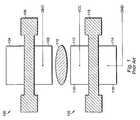
- FIG. 6Ca cross-sectional view 432 of one of the transistors shown in FIG. 5 is taken along the axis of the polysilicon gate.
- the semiconductor substrate or epitaxial layer 446is shown.
- the gate oxide layer 448is shown, within the boundary of the active area, surrounded by thick field oxide layer 438 on both sides.
- the polysilicon or metal gate 418is shown, which is covered over by oxide layer 436 .
- the isolating metal region 422 overlapping the active layeris shown, as well as a single contact 440 for providing electrical access to gate 418 .
- FIG. 6Bis a cross-sectional view 434 of one of the transistors shown in FIG. 4 or FIG. 5 taken across the axis of the polysilicon gate.
- the semiconductor substrate or epitaxial layer 446is shown, including source/drain regions 410 and 414 .
- the gate oxide layer 448is shown, within the boundary of the active area, surrounded by thick field oxide layer 438 on both sides.
- the polysilicon or metal gate 418is shown defining the source/drain regions 410 and 414 , which is then all covered over by oxide layer 436 .
- the isolating metal region 422 overlapping the active layeris shown, as well as two contacts 442 and 444 for providing electrical access to source/drain regions 410 and 414 .
- Radiation-hardened device 700includes an active region 702 surrounded by thick oxide, first and second polysilicon or metal gates 710 and 712 crossing the active region 702 , defining first, second, and third source/drain regions 704 , 706 , and 708 , and a metal region 714 coupled to ground overlapping the boundary of the active region 702 , and completely surrounding each of the ends of the first and second gates 710 and 712 that extend beyond the border of the active region 702 , wherein the first source/drain region 704 defines the source/drain region of a first N-channel transistor, the third source/drain region 708 defines the source/drain region of a second N-channel transistor, and the second source/drain region 706 defines a common source/drain region for the first and second N-channel transistors.
- either the first or third source/drain regions 704 and 708are coupled to ground, so that the device is suitable for use in a NAND gate.
- the first and third source/drain regions 704 and 708are coupled to ground, so that the device is suitable for use in a NOR gate.
- the metal region 714 overlapping the boundary of the active region 702can be made to completely surround the first end of the first and second gates 710 and 712 that extend beyond the border of the active region, and to completely cover the second end of the first and second gates 710 and 712 that extend beyond the border of the active region, as was shown in FIG. 5 .
- the radiation-hardened N-channel transistor and device of the present inventionaddresses the problem of impinging ionizing radiation, these transistors may oftentimes be integrated onto a circuit with other P-channel transistors fabricated inside of a lightly doped N-type well. If steps are not taken to account for these other transistors, there may be undesirable leakage current as is explained in further detail below. This problem is exacerbated in integrated circuits in which two or more well bias voltages are found.
- FIG. 8a cross-sectional view 800 of an N-channel transistor 804 and a P-channel transistor in a lightly doped well 802 .
- metal regions 806are coupled to ground or to the lowest potential in the circuit to prevent leakage current due to ionizing radiation.
- N-channel transistor 804is fabricated according to the present invention, then additional metal regions are not required, since the metal regions associated with transistor 804 itself will be sufficient to stop the leakage current.
- N-channel transistor 904is formed in a lightly doped P-type well
- P-channel transistor 902is formed in a lightly doped N-type well.
- FIG. 10a cross-sectional view 1000 of two P-channel transistors 1004 and 1006 formed in lightly doped N-type wells is shown.
- the wellsare formed in epitaxial layer or substrate 1002 as is known in the art.
- the wells of transistors 1004 and 1006can be biased to different biasing voltages.
- the N-type well of transistor 1004is biased to one volt at node or pad 1010
- the N-type well of transistor 1006is biased to two volts at node or pad 1012 .
- a metal region 1008is provided as shown. Metal region 1008 is coupled to ground or to the lowest voltage in the integrated circuit. It should be noted that the radiation-induced leakage current in area 1018 is similar in effect to the intra-device leakage current 118 as explained with respect to transistor 102 shown in FIG. 1 .
- a simplified plan view 1100 of a metal layout for a small portion of an integrated circuitis shown.
- a plurality of N-channel transistors 1102 formed in P-type wellsinclude ringed metal areas 1106 (not shown in detail in FIG. 11 , best shown in FIGS. 4 and 5 ) according to the present invention.
- a plurality of P-channel transistors 1104 A, 1104 B, 1104 C and 1104 Dare formed in N-type wells, and are adjacent to the plurality of transistors 1102 . Note that the well of transistor 1104 A is biased to one volt at node 1110 , and the well of transistor 1104 B is biased to two volts at node 1112 .
- the ringed metal regions 1106 of the N-channel transistors 1102are joined together with the metal regions 1108 used to isolate the P-channel transistors 1104 A-D for receiving a ground or lowest potential voltage at node 1114 for the purposes of providing optimum radiation hardening.
- the metal scheme shown in FIG. 11can be expanded to an entire integrated circuit device for the purpose of virtually eliminating all possible paths of radiation-induced inter-device and intra-device leakage currents between and within transistors, whether formed in a well, or directly in the epitaxial layer or substrate.
Landscapes
- Insulated Gate Type Field-Effect Transistor (AREA)
- Metal-Oxide And Bipolar Metal-Oxide Semiconductor Integrated Circuits (AREA)
Abstract
Description
Claims (3)
Priority Applications (1)
| Application Number | Priority Date | Filing Date | Title |
|---|---|---|---|
| US11/687,588US7737535B2 (en) | 2005-03-03 | 2007-03-16 | Total ionizing dose suppression transistor architecture |
Applications Claiming Priority (2)
| Application Number | Priority Date | Filing Date | Title |
|---|---|---|---|
| US11/071,730US7518218B2 (en) | 2005-03-03 | 2005-03-03 | Total ionizing dose suppression transistor architecture |
| US11/687,588US7737535B2 (en) | 2005-03-03 | 2007-03-16 | Total ionizing dose suppression transistor architecture |
Related Parent Applications (1)
| Application Number | Title | Priority Date | Filing Date |
|---|---|---|---|
| US11/071,730DivisionUS7518218B2 (en) | 2005-03-03 | 2005-03-03 | Total ionizing dose suppression transistor architecture |
Publications (2)
| Publication Number | Publication Date |
|---|---|
| US20070181978A1 US20070181978A1 (en) | 2007-08-09 |
| US7737535B2true US7737535B2 (en) | 2010-06-15 |
Family
ID=36943292
Family Applications (2)
| Application Number | Title | Priority Date | Filing Date |
|---|---|---|---|
| US11/071,730Expired - LifetimeUS7518218B2 (en) | 2005-03-03 | 2005-03-03 | Total ionizing dose suppression transistor architecture |
| US11/687,588Active2026-07-04US7737535B2 (en) | 2005-03-03 | 2007-03-16 | Total ionizing dose suppression transistor architecture |
Family Applications Before (1)
| Application Number | Title | Priority Date | Filing Date |
|---|---|---|---|
| US11/071,730Expired - LifetimeUS7518218B2 (en) | 2005-03-03 | 2005-03-03 | Total ionizing dose suppression transistor architecture |
Country Status (1)
| Country | Link |
|---|---|
| US (2) | US7518218B2 (en) |
Cited By (1)
| Publication number | Priority date | Publication date | Assignee | Title |
|---|---|---|---|---|
| US9438025B1 (en)* | 2013-03-11 | 2016-09-06 | Defense Electronics Corporation | Radiation hardened chip level integrated recovery apparatus, methods, and integrated circuits |
Families Citing this family (15)
| Publication number | Priority date | Publication date | Assignee | Title |
|---|---|---|---|---|
| US7518218B2 (en)* | 2005-03-03 | 2009-04-14 | Aeroflex Colorado Springs, Inc. | Total ionizing dose suppression transistor architecture |
| US9396947B2 (en) | 2011-08-25 | 2016-07-19 | Aeroflex Colorado Springs Inc. | Wafer structure for electronic integrated circuit manufacturing |
| US9378955B2 (en) | 2011-08-25 | 2016-06-28 | Aeroflex Colorado Springs Inc. | Wafer structure for electronic integrated circuit manufacturing |
| US9312133B2 (en) | 2011-08-25 | 2016-04-12 | Aeroflex Colorado Springs Inc. | Wafer structure for electronic integrated circuit manufacturing |
| WO2013028976A1 (en)* | 2011-08-25 | 2013-02-28 | Aeroflex Colorado Springs Inc. | Wafer structure for electronic integrated circuit manufacturing |
| US9378956B2 (en) | 2011-08-25 | 2016-06-28 | Aeroflex Colorado Springs Inc. | Wafer structure for electronic integrated circuit manufacturing |
| WO2013078439A2 (en) | 2011-11-22 | 2013-05-30 | Silicon Space Technology Corporation | Memory circuit incorporating radiation hardened memory scrub engine |
| CN102832250B (en)* | 2012-09-14 | 2015-06-10 | 电子科技大学 | Irradiation-resistant metal-oxide-semiconductor field-effect transistor (MOSFET)for partitioning ring grating |
| US9268637B2 (en) | 2013-03-15 | 2016-02-23 | Silicon Space Technology Corporation | Memory circuit incorporating error detection and correction (EDAC), method of operation, and system |
| TW201603227A (en)* | 2014-07-15 | 2016-01-16 | 頎邦科技股份有限公司 | Routing structure for fine-pitch pattern |
| CN107516677A (en)* | 2016-06-17 | 2017-12-26 | 上海新微科技服务有限公司 | A MOS Field Effect Transistor |
| CN113178487A (en)* | 2020-01-24 | 2021-07-27 | 台湾积体电路制造股份有限公司 | Semiconductor device with a plurality of transistors |
| CN111987152B (en)* | 2020-09-09 | 2024-01-26 | 电子科技大学 | Anti-radiation double-gate LDMOS device structure |
| US12094879B2 (en)* | 2022-09-23 | 2024-09-17 | Apogee Semiconductor, Inc. | MOS devices for sensing total ionizing dose |
| US11784250B1 (en) | 2023-02-02 | 2023-10-10 | Apogee Semiconductor, Inc. | Devices and methods for compact radiation-hardened integrated circuits |
Citations (17)
| Publication number | Priority date | Publication date | Assignee | Title |
|---|---|---|---|---|
| US6091630A (en) | 1999-09-10 | 2000-07-18 | Stmicroelectronics, Inc. | Radiation hardened semiconductor memory |
| US6225178B1 (en) | 1990-01-02 | 2001-05-01 | Honeywell Inc. | Radiation hardened field oxide for VLSI sub-micron MOS device |
| US6225667B1 (en) | 2000-01-18 | 2001-05-01 | Advanced Micro Devices, Inc. | Leaky lower interface for reduction of floating body effect in SOI devices |
| US6380598B1 (en) | 1994-12-20 | 2002-04-30 | Stmicroelectronics, Inc. | Radiation hardened semiconductor memory |
| US6455884B1 (en) | 1999-10-22 | 2002-09-24 | Stmicroelectronics, Inc. | Radiation hardened semiconductor memory with active isolation regions |
| US20020171104A1 (en) | 2001-04-05 | 2002-11-21 | Cable James S. | Radiation-hardened silicon-on-insulator CMOS device, and method of making the same |
| US6511893B1 (en) | 1998-05-05 | 2003-01-28 | Aeroflex Utmc Microelectronics, Inc. | Radiation hardened semiconductor device |
| US20030022527A1 (en) | 2001-06-21 | 2003-01-30 | Devine Roderick A. B. | Radiation hardened microcircuits |
| US20030036236A1 (en) | 2001-08-15 | 2003-02-20 | Joseph Benedetto | Method for radiation hardening N-channel MOS transistors |
| US20030058027A1 (en) | 2001-09-27 | 2003-03-27 | Kwon Gue-Hyung | Circuits and methods for electrostatic discharge protection in integrated circuits |
| US6570234B1 (en) | 1999-11-17 | 2003-05-27 | Aeroflex Utmc Microelectronic Systems, Inc. | Radiation resistant integrated circuit design |
| US20040056333A1 (en)* | 2002-09-24 | 2004-03-25 | Lin Hung Chang | Electromagnetic traps in integrated circuit for minimizing cross-talk |
| US6730969B1 (en) | 2002-06-27 | 2004-05-04 | National Semiconductor Corporation | Radiation hardened MOS transistor |
| US6744661B1 (en) | 2002-05-15 | 2004-06-01 | Virage Logic Corp. | Radiation-hardened static memory cell using isolation technology |
| US6777753B1 (en) | 2000-07-12 | 2004-08-17 | The United States Of America As Represented By The Secretary Of The Navy | CMOS devices hardened against total dose radiation effects |
| US20050056889A1 (en) | 2003-09-15 | 2005-03-17 | Gordon Ma | LDMOS transistor |
| US7518218B2 (en)* | 2005-03-03 | 2009-04-14 | Aeroflex Colorado Springs, Inc. | Total ionizing dose suppression transistor architecture |
Family Cites Families (4)
| Publication number | Priority date | Publication date | Assignee | Title |
|---|---|---|---|---|
| JPH1042017A (en)* | 1996-07-19 | 1998-02-13 | Nec Corp | Transmitting part structure |
| US5990214A (en)* | 1997-07-31 | 1999-11-23 | Velsicol Chemical Corporation | Liquid glycol benzoate compositions |
| US6225687B1 (en)* | 1999-09-02 | 2001-05-01 | Intel Corporation | Chip package with degassing holes |
| US6940681B2 (en)* | 2001-08-20 | 2005-09-06 | Quantum Corporation | Optical to magnetic alignment in magnetic tape system |
- 2005
- 2005-03-03USUS11/071,730patent/US7518218B2/ennot_activeExpired - Lifetime
- 2007
- 2007-03-16USUS11/687,588patent/US7737535B2/enactiveActive
Patent Citations (25)
| Publication number | Priority date | Publication date | Assignee | Title |
|---|---|---|---|---|
| US6225178B1 (en) | 1990-01-02 | 2001-05-01 | Honeywell Inc. | Radiation hardened field oxide for VLSI sub-micron MOS device |
| US6656803B2 (en) | 1994-12-20 | 2003-12-02 | Stmicrocelectronics, Inc. | Radiation hardened semiconductor memory |
| US6380598B1 (en) | 1994-12-20 | 2002-04-30 | Stmicroelectronics, Inc. | Radiation hardened semiconductor memory |
| US20020086461A1 (en) | 1994-12-20 | 2002-07-04 | Stmicroelectronics, Inc. | Radiation hardened semiconductor memory |
| US20040166648A1 (en) | 1998-05-05 | 2004-08-26 | Woodruff Richard L. | Radiation hardened semiconductor device |
| US6511893B1 (en) | 1998-05-05 | 2003-01-28 | Aeroflex Utmc Microelectronics, Inc. | Radiation hardened semiconductor device |
| US6194276B1 (en) | 1999-09-10 | 2001-02-27 | Stmicroelectronics, Inc. | Radiation hardened semiconductor memory |
| US6091630A (en) | 1999-09-10 | 2000-07-18 | Stmicroelectronics, Inc. | Radiation hardened semiconductor memory |
| US6455884B1 (en) | 1999-10-22 | 2002-09-24 | Stmicroelectronics, Inc. | Radiation hardened semiconductor memory with active isolation regions |
| US6570234B1 (en) | 1999-11-17 | 2003-05-27 | Aeroflex Utmc Microelectronic Systems, Inc. | Radiation resistant integrated circuit design |
| US6225667B1 (en) | 2000-01-18 | 2001-05-01 | Advanced Micro Devices, Inc. | Leaky lower interface for reduction of floating body effect in SOI devices |
| US6417030B1 (en) | 2000-01-18 | 2002-07-09 | Advanced Micro Devices, Inc. | Leaky lower interface for reduction of floating body effect in SOI devices |
| US6777753B1 (en) | 2000-07-12 | 2004-08-17 | The United States Of America As Represented By The Secretary Of The Navy | CMOS devices hardened against total dose radiation effects |
| US6531739B2 (en) | 2001-04-05 | 2003-03-11 | Peregrine Semiconductor Corporation | Radiation-hardened silicon-on-insulator CMOS device, and method of making the same |
| US20030173591A1 (en) | 2001-04-05 | 2003-09-18 | Cable James S. | Radiation-hardened silicon-on-insulator CMOS device, and method of making the same |
| US20020171104A1 (en) | 2001-04-05 | 2002-11-21 | Cable James S. | Radiation-hardened silicon-on-insulator CMOS device, and method of making the same |
| US20030022527A1 (en) | 2001-06-21 | 2003-01-30 | Devine Roderick A. B. | Radiation hardened microcircuits |
| US20030143811A1 (en) | 2001-08-15 | 2003-07-31 | Joseph Benedetto | Method for radiation hardening N-channel MOS transistors |
| US20030036236A1 (en) | 2001-08-15 | 2003-02-20 | Joseph Benedetto | Method for radiation hardening N-channel MOS transistors |
| US20030058027A1 (en) | 2001-09-27 | 2003-03-27 | Kwon Gue-Hyung | Circuits and methods for electrostatic discharge protection in integrated circuits |
| US6744661B1 (en) | 2002-05-15 | 2004-06-01 | Virage Logic Corp. | Radiation-hardened static memory cell using isolation technology |
| US6730969B1 (en) | 2002-06-27 | 2004-05-04 | National Semiconductor Corporation | Radiation hardened MOS transistor |
| US20040056333A1 (en)* | 2002-09-24 | 2004-03-25 | Lin Hung Chang | Electromagnetic traps in integrated circuit for minimizing cross-talk |
| US20050056889A1 (en) | 2003-09-15 | 2005-03-17 | Gordon Ma | LDMOS transistor |
| US7518218B2 (en)* | 2005-03-03 | 2009-04-14 | Aeroflex Colorado Springs, Inc. | Total ionizing dose suppression transistor architecture |
Cited By (2)
| Publication number | Priority date | Publication date | Assignee | Title |
|---|---|---|---|---|
| US9438025B1 (en)* | 2013-03-11 | 2016-09-06 | Defense Electronics Corporation | Radiation hardened chip level integrated recovery apparatus, methods, and integrated circuits |
| US9720026B1 (en) | 2013-03-11 | 2017-08-01 | Defense Electronics Corporation | Radiation hardened chip level integrated recovery apparatus, methods, and integrated circuits |
Also Published As
| Publication number | Publication date |
|---|---|
| US7518218B2 (en) | 2009-04-14 |
| US20070181978A1 (en) | 2007-08-09 |
| US20060197108A1 (en) | 2006-09-07 |
Similar Documents
| Publication | Publication Date | Title |
|---|---|---|
| US7737535B2 (en) | Total ionizing dose suppression transistor architecture | |
| US7808056B2 (en) | Semiconductor integrated circuit device | |
| JP3887326B2 (en) | Protective structure that prevents the propagation of defects generated in semiconductor devices | |
| US6570234B1 (en) | Radiation resistant integrated circuit design | |
| EP0782192B1 (en) | Electrostatic discharge structure of semiconductor device | |
| KR101023078B1 (en) | Semiconductor element and manufacturing method thereof | |
| JP3719650B2 (en) | Semiconductor device | |
| US11830740B2 (en) | Mask layout, semiconductor device and manufacturing method using the same | |
| US20030197242A1 (en) | Structure and fabrication method of electrostatic discharge protection circuit | |
| JP2002100761A (en) | Silicon MOSFET high frequency semiconductor device and method of manufacturing the same | |
| US6278162B1 (en) | ESD protection for LDD devices | |
| US8587023B2 (en) | Guard rings with local coupling capacitance | |
| EP0066429A2 (en) | Semiconductor memory | |
| KR100613819B1 (en) | Silicon-on-insulator latch-up pulse-radiation detector | |
| US8283726B2 (en) | System and method for I/O ESD protection with polysilicon regions fabricated by processes for making core transistors | |
| US6399989B1 (en) | Radiation hardened silicon-on-insulator (SOI) transistor having a body contact | |
| JPH044755B2 (en) | ||
| US10366978B1 (en) | Grounded gate NMOS transistor having source pulled back region | |
| US6366435B1 (en) | Multiple sources ESD protection for an epitaxy wafer substrate | |
| US8686507B2 (en) | System and method for I/O ESD protection with floating and/or biased polysilicon regions | |
| US6818955B1 (en) | Electrostatic discharge protection | |
| JPH07106571A (en) | Semiconductor device | |
| US8319286B2 (en) | System and method for input pin ESD protection with floating and/or biased polysilicon regions | |
| JPH1168043A (en) | ESD protection circuit | |
| JP3175870B2 (en) | Semiconductor device with electrostatic protection function and method of manufacturing the same |
Legal Events
| Date | Code | Title | Description |
|---|---|---|---|
| AS | Assignment | Owner name:AEROFLEX COLORADO SPRINGS INC.,COLORADO Free format text:ASSIGNMENT OF ASSIGNORS INTEREST;ASSIGNOR:GARDNER, HARRY N.;REEL/FRAME:019025/0978 Effective date:20050225 Owner name:AEROFLEX COLORADO SPRINGS INC., COLORADO Free format text:ASSIGNMENT OF ASSIGNORS INTEREST;ASSIGNOR:GARDNER, HARRY N.;REEL/FRAME:019025/0978 Effective date:20050225 | |
| AS | Assignment | Owner name:GOLDMAN SACHS CREDIT PARTNERS, L.P., AS COLLATERAL Free format text:SECURITY AGREEMENT;ASSIGNOR:AEROFLEX COLORADO SPRINGS, INC.;REEL/FRAME:019834/0442 Effective date:20070815 | |
| STCF | Information on status: patent grant | Free format text:PATENTED CASE | |
| FEPP | Fee payment procedure | Free format text:PAYOR NUMBER ASSIGNED (ORIGINAL EVENT CODE: ASPN); ENTITY STATUS OF PATENT OWNER: LARGE ENTITY | |
| AS | Assignment | Owner name:AEROFLEX COLORADO SPRINGS, INC., COLORADO Free format text:RELEASE OF SECURITY INTEREST IN INTELLECTUAL PROPERTY COLLATERAL;ASSIGNOR:GOLDMAN SACHS CREDIT PARTNERS, L.P., AS COLLATERAL AGENT;REEL/FRAME:026247/0469 Effective date:20110509 | |
| AS | Assignment | Owner name:JPMORGAN CHASE BANK, NA, AS COLLATERAL AGENT, NEW Free format text:SECURITY AGREEMENT;ASSIGNORS:AEROFLEX INCORPORATED;AEROFLEX/WEINSCHEL, INC.;AEROFLEX COLORADO SPRINGS, INC.;AND OTHERS;REEL/FRAME:026422/0719 Effective date:20110509 | |
| FPAY | Fee payment | Year of fee payment:4 | |
| AS | Assignment | Owner name:AEROFLEX MICROELECTRONIC SOLUTIONS, INC., MICHIGAN Free format text:RELEASE OF PATENT SECURITY INTEREST;ASSIGNOR:JPMRGAN CHASE BANK, N.A.;REEL/FRAME:033728/0942 Effective date:20140912 Owner name:AEROFLEX INCORPORATED, NEW YORK Free format text:RELEASE OF PATENT SECURITY INTEREST;ASSIGNOR:JPMRGAN CHASE BANK, N.A.;REEL/FRAME:033728/0942 Effective date:20140912 Owner name:AEROFLEX PLAINVIEW, INC., NEW YORK Free format text:RELEASE OF PATENT SECURITY INTEREST;ASSIGNOR:JPMRGAN CHASE BANK, N.A.;REEL/FRAME:033728/0942 Effective date:20140912 Owner name:AEROFLEX WICHITA, INC., KANSAS Free format text:RELEASE OF PATENT SECURITY INTEREST;ASSIGNOR:JPMRGAN CHASE BANK, N.A.;REEL/FRAME:033728/0942 Effective date:20140912 Owner name:AEROFLEX SYSTEMS GROUP, INC., CALIFORNIA Free format text:RELEASE OF PATENT SECURITY INTEREST;ASSIGNOR:JPMRGAN CHASE BANK, N.A.;REEL/FRAME:033728/0942 Effective date:20140912 Owner name:AEROFLEX COLORADO SPRINGS, INC., COLORADO Free format text:RELEASE OF PATENT SECURITY INTEREST;ASSIGNOR:JPMRGAN CHASE BANK, N.A.;REEL/FRAME:033728/0942 Effective date:20140912 Owner name:AEROFLEX/WEINSCHEL, INC., MARYLAND Free format text:RELEASE OF PATENT SECURITY INTEREST;ASSIGNOR:JPMRGAN CHASE BANK, N.A.;REEL/FRAME:033728/0942 Effective date:20140912 | |
| FEPP | Fee payment procedure | Free format text:MAINTENANCE FEE REMINDER MAILED (ORIGINAL EVENT CODE: REM.) | |
| FEPP | Fee payment procedure | Free format text:7.5 YR SURCHARGE - LATE PMT W/IN 6 MO, LARGE ENTITY (ORIGINAL EVENT CODE: M1555) | |
| MAFP | Maintenance fee payment | Free format text:PAYMENT OF MAINTENANCE FEE, 8TH YEAR, LARGE ENTITY (ORIGINAL EVENT CODE: M1552) Year of fee payment:8 | |
| AS | Assignment | Owner name:COBHAM COLORADO SPRINGS INC., COLORADO Free format text:CHANGE OF NAME;ASSIGNOR:AEROFLEX COLORADO SPRINGS, INC.;REEL/FRAME:055847/0958 Effective date:20190102 | |
| MAFP | Maintenance fee payment | Free format text:PAYMENT OF MAINTENANCE FEE, 12TH YEAR, LARGE ENTITY (ORIGINAL EVENT CODE: M1553); ENTITY STATUS OF PATENT OWNER: LARGE ENTITY Year of fee payment:12 | |
| AS | Assignment | Owner name:CAES COLORADO SPRINGS LLC, VIRGINIA Free format text:ENTITY CONVERSION;ASSIGNOR:COBHAM COLORADO SPRINGS INC.;REEL/FRAME:061299/0532 Effective date:20211221 Owner name:CAES COLORADO SPRINGS LLC, VIRGINIA Free format text:ENTITY CONVERSION;ASSIGNOR:COBHAM COLORADO SPRINGS INC.;REEL/FRAME:061299/0490 Effective date:20211221 | |
| AS | Assignment | Owner name:JPMORGAN CHASE BANK, N.A., AS COLLATERAL AGENT, ILLINOIS Free format text:SECURITY INTEREST;ASSIGNORS:CAES COLORADO SPRINGS LLC;COBHAM ADVANCED ELECTRONIC SOLUTIONS INC.;REEL/FRAME:062337/0939 Effective date:20230109 | |
| AS | Assignment | Owner name:FRONTGRADE COLORADO SPRINGS LLC, COLORADO Free format text:CHANGE OF NAME;ASSIGNOR:CAES COLORADO SPRINGS LLC;REEL/FRAME:068326/0038 Effective date:20230123 |