US7737483B2 - Low resistance void-free contacts - Google Patents
Low resistance void-free contactsDownload PDFInfo
- Publication number
- US7737483B2 US7737483B2US11/296,235US29623505AUS7737483B2US 7737483 B2US7737483 B2US 7737483B2US 29623505 AUS29623505 AUS 29623505AUS 7737483 B2US7737483 B2US 7737483B2
- Authority
- US
- United States
- Prior art keywords
- nonvolatile memory
- memory array
- layer
- substrate
- dielectric
- Prior art date
- Legal status (The legal status is an assumption and is not a legal conclusion. Google has not performed a legal analysis and makes no representation as to the accuracy of the status listed.)
- Expired - Fee Related, expires
Links
- 239000000463materialSubstances0.000claimsabstractdescription57
- 230000015654memoryEffects0.000claimsdescription62
- 238000007667floatingMethods0.000claimsdescription38
- 239000000758substrateSubstances0.000claimsdescription37
- 229910021420polycrystalline siliconInorganic materials0.000claimsdescription27
- 229920005591polysiliconPolymers0.000claimsdescription27
- 239000002131composite materialSubstances0.000claimsdescription21
- 239000003989dielectric materialSubstances0.000claimsdescription15
- WFKWXMTUELFFGS-UHFFFAOYSA-NtungstenChemical compound[W]WFKWXMTUELFFGS-UHFFFAOYSA-N0.000claimsdescription15
- 229910052721tungstenInorganic materials0.000claimsdescription15
- 239000010937tungstenSubstances0.000claimsdescription15
- 230000004888barrier functionEffects0.000claimsdescription5
- 238000002955isolationMethods0.000claimsdescription4
- 239000010936titaniumSubstances0.000claimsdescription3
- RTAQQCXQSZGOHL-UHFFFAOYSA-NTitaniumChemical compound[Ti]RTAQQCXQSZGOHL-UHFFFAOYSA-N0.000claimsdescription2
- NRTOMJZYCJJWKI-UHFFFAOYSA-NTitanium nitrideChemical compound[Ti]#NNRTOMJZYCJJWKI-UHFFFAOYSA-N0.000claimsdescription2
- 229910052719titaniumInorganic materials0.000claimsdescription2
- 238000000151depositionMethods0.000abstractdescription19
- 239000004020conductorSubstances0.000description48
- 230000008021depositionEffects0.000description17
- 238000000034methodMethods0.000description12
- VYPSYNLAJGMNEJ-UHFFFAOYSA-NSilicium dioxideChemical compoundO=[Si]=OVYPSYNLAJGMNEJ-UHFFFAOYSA-N0.000description11
- 238000003491arrayMethods0.000description7
- 230000015572biosynthetic processEffects0.000description7
- 238000003860storageMethods0.000description7
- 230000008878couplingEffects0.000description6
- 238000010168coupling processMethods0.000description6
- 238000005859coupling reactionMethods0.000description6
- 239000012535impuritySubstances0.000description5
- 239000000377silicon dioxideSubstances0.000description5
- 239000011800void materialSubstances0.000description5
- BOTDANWDWHJENH-UHFFFAOYSA-NTetraethyl orthosilicateChemical compoundCCO[Si](OCC)(OCC)OCCBOTDANWDWHJENH-UHFFFAOYSA-N0.000description4
- 238000005530etchingMethods0.000description4
- 229910052581Si3N4Inorganic materials0.000description3
- XUIMIQQOPSSXEZ-UHFFFAOYSA-NSiliconChemical compound[Si]XUIMIQQOPSSXEZ-UHFFFAOYSA-N0.000description3
- 229910052782aluminiumInorganic materials0.000description3
- XAGFODPZIPBFFR-UHFFFAOYSA-NaluminiumChemical compound[Al]XAGFODPZIPBFFR-UHFFFAOYSA-N0.000description3
- 239000005380borophosphosilicate glassSubstances0.000description3
- 238000004518low pressure chemical vapour depositionMethods0.000description3
- 229910052751metalInorganic materials0.000description3
- 239000002184metalSubstances0.000description3
- 238000012545processingMethods0.000description3
- 229910052710siliconInorganic materials0.000description3
- 239000010703siliconSubstances0.000description3
- 235000012239silicon dioxideNutrition0.000description3
- HQVNEWCFYHHQES-UHFFFAOYSA-Nsilicon nitrideChemical compoundN12[Si]34N5[Si]62N3[Si]51N64HQVNEWCFYHHQES-UHFFFAOYSA-N0.000description3
- 238000013459approachMethods0.000description2
- 238000005229chemical vapour depositionMethods0.000description2
- 238000010586diagramMethods0.000description2
- 239000002019doping agentSubstances0.000description2
- 230000006870functionEffects0.000description2
- 238000004519manufacturing processMethods0.000description2
- 150000004767nitridesChemical class0.000description2
- 238000000059patterningMethods0.000description2
- 238000001020plasma etchingMethods0.000description2
- ZOXJGFHDIHLPTG-UHFFFAOYSA-NBoronChemical compound[B]ZOXJGFHDIHLPTG-UHFFFAOYSA-N0.000description1
- RYGMFSIKBFXOCR-UHFFFAOYSA-NCopperChemical compound[Cu]RYGMFSIKBFXOCR-UHFFFAOYSA-N0.000description1
- 229910052785arsenicInorganic materials0.000description1
- RQNWIZPPADIBDY-UHFFFAOYSA-Narsenic atomChemical compound[As]RQNWIZPPADIBDY-UHFFFAOYSA-N0.000description1
- 229910052796boronInorganic materials0.000description1
- 230000001413cellular effectEffects0.000description1
- 238000004891communicationMethods0.000description1
- 229910052802copperInorganic materials0.000description1
- 239000010949copperSubstances0.000description1
- 230000001419dependent effectEffects0.000description1
- 238000009792diffusion processMethods0.000description1
- 238000005516engineering processMethods0.000description1
- 238000010438heat treatmentMethods0.000description1
- BHEPBYXIRTUNPN-UHFFFAOYSA-Nhydridophosphorus(.) (triplet)Chemical compound[PH]BHEPBYXIRTUNPN-UHFFFAOYSA-N0.000description1
- 238000002513implantationMethods0.000description1
- 230000001788irregularEffects0.000description1
- 238000005498polishingMethods0.000description1
- 230000008569processEffects0.000description1
- 239000003870refractory metalSubstances0.000description1
- 229910052814silicon oxideInorganic materials0.000description1
- 239000000126substanceSubstances0.000description1
Images


Classifications
- H—ELECTRICITY
- H10—SEMICONDUCTOR DEVICES; ELECTRIC SOLID-STATE DEVICES NOT OTHERWISE PROVIDED FOR
- H10B—ELECTRONIC MEMORY DEVICES
- H10B41/00—Electrically erasable-and-programmable ROM [EEPROM] devices comprising floating gates
- H10B41/30—Electrically erasable-and-programmable ROM [EEPROM] devices comprising floating gates characterised by the memory core region
- H—ELECTRICITY
- H01—ELECTRIC ELEMENTS
- H01L—SEMICONDUCTOR DEVICES NOT COVERED BY CLASS H10
- H01L21/00—Processes or apparatus adapted for the manufacture or treatment of semiconductor or solid state devices or of parts thereof
- H01L21/70—Manufacture or treatment of devices consisting of a plurality of solid state components formed in or on a common substrate or of parts thereof; Manufacture of integrated circuit devices or of parts thereof
- H01L21/71—Manufacture of specific parts of devices defined in group H01L21/70
- H01L21/768—Applying interconnections to be used for carrying current between separate components within a device comprising conductors and dielectrics
- H01L21/76838—Applying interconnections to be used for carrying current between separate components within a device comprising conductors and dielectrics characterised by the formation and the after-treatment of the conductors
- H01L21/76877—Filling of holes, grooves or trenches, e.g. vias, with conductive material
- H—ELECTRICITY
- H10—SEMICONDUCTOR DEVICES; ELECTRIC SOLID-STATE DEVICES NOT OTHERWISE PROVIDED FOR
- H10B—ELECTRONIC MEMORY DEVICES
- H10B41/00—Electrically erasable-and-programmable ROM [EEPROM] devices comprising floating gates
- H10B41/30—Electrically erasable-and-programmable ROM [EEPROM] devices comprising floating gates characterised by the memory core region
- H10B41/35—Electrically erasable-and-programmable ROM [EEPROM] devices comprising floating gates characterised by the memory core region with a cell select transistor, e.g. NAND
- H—ELECTRICITY
- H10—SEMICONDUCTOR DEVICES; ELECTRIC SOLID-STATE DEVICES NOT OTHERWISE PROVIDED FOR
- H10B—ELECTRONIC MEMORY DEVICES
- H10B69/00—Erasable-and-programmable ROM [EPROM] devices not provided for in groups H10B41/00 - H10B63/00, e.g. ultraviolet erasable-and-programmable ROM [UVEPROM] devices
Definitions
- This inventionrelates to flash memory arrays and in particular to the structures of flash memory arrays and methods of forming them.
- Nonvolatile memory productsare used today, particularly in the form of small form factor cards, which use an array of flash EEPROM (Electrically Erasable and Programmable Read Only Memory) cells.
- Such cardsmay be interfaced with a host, for example, by removably inserting a card into a card slot in a host.
- Some of the commercially available cardsare CompactFlashTM (CF) cards, MultiMedia cards (MMC), Secure Digital (SD) cards, Smart Media cards, personnel tags (P-Tag) and Memory Stick cards.
- Hostsinclude personal computers, notebook computers, personal digital assistants (PDAs), various data communication devices, digital cameras, cellular telephones, portable audio players, automobile sound systems, and similar types of equipment.
- PDAspersonal digital assistants
- a memory systemis permanently connected to a host providing an embedded memory that is dedicated to the host.
- NOR and NANDTwo general memory cell array architectures have found commercial application, NOR and NAND.
- memory cellsare connected between adjacent bit line source and drain diffusions that extend in a column direction with control gates connected to word lines extending along rows of cells.
- a memory cellincludes at least one storage element positioned over at least a portion of the cell channel region between the source and drain. A programmed level of charge on the storage elements thus controls an operating characteristic of the cells, which can then be read by applying appropriate voltages to the addressed memory cells. Examples of such cells, their uses in memory systems and methods of manufacturing them are given in the following U.S. Pat. Nos.
- NAND arrayseries strings of more than two memory cells, such as 16 or 32, are connected along with one or more select transistors between individual bit lines and a reference potential to form columns of cells. Word lines extend across cells within a large number of these columns. An individual cell within a column is read and verified during programming by causing the remaining cells in the string to be turned on hard so that the current flowing through a string is dependent upon the level of charge stored in the addressed cell.
- An example of a NAND architecture array and its operation as part of a memory systemis found in the following U.S. Pat. Nos. 5,570,315; 5,774,397; 6,046,935 and 6,522,580. NAND memory devices have been found to be particularly suitable for mass storage applications such as those using removable memory cards.
- the charge storage elements of current flash EEPROM arraysare most commonly electrically conductive floating gates, typically formed from conductively doped polysilicon material.
- An alternate type of memory cell useful in flash EEPROM systemsutilizes a non-conductive dielectric material in place of the conductive floating gate to store charge in a non-volatile manner.
- a triple layer dielectric formed of silicon dioxide, silicon nitride and silicon oxide (ONO)is sandwiched between a conductive control gate and a surface of a semi-conductive substrate above the memory cell channel.
- the cellis programmed by injecting electrons from the cell channel into the nitride, where they are trapped and stored in a limited region, and erased by injecting hot holes into the nitride.
- flash EEPROM systemsAs in most integrated circuit applications, the pressure to shrink the silicon substrate area required to implement some integrated circuit function also exists with flash EEPROM systems. It is continually desired to increase the amount of digital data that can be stored in a given area of a silicon substrate, in order to increase the storage capacity of a given size memory card and other types of packages, or to both increase capacity and decrease size.
- One way to increase the storage density of datais to store more than one bit of data per memory cell. This is accomplished by dividing a window of a floating gate charge level voltage range into more than two states. The use of four such states allows each cell to store two bits of data, eight states stores three bits of data per cell, and so on.
- a multiple state flash EEPROM structure and operationis described in U.S. Pat. Nos. 5,043,940 and 5,172,338, which patents are incorporated herein by this reference.
- Increased data densitycan also be achieved by reducing the physical size of the memory cells and/or the overall array.
- Shrinking the size of integrated circuitsis commonly performed for all types of circuits as processing techniques improve over time to permit implementing smaller feature sizes. But there are usually limits of how far a given circuit layout can be shrunk in this manner, since there is often at least one feature that is limited as to how much, it can be shrunk. When this happens, designers will turn to a new or different layout or architecture of the circuit being implemented in order to reduce the amount of silicon area required to perform its functions. The shrinking of the above-described flash EEPROM integrated circuit systems can reach such limits.
- STIShallow Trench Isolation
- Thisuses STI structures to isolate adjacent strings of floating gate cells such as those of NAND type memory arrays.
- a gate dielectric (tunnel dielectric) layer and floating gate polysilicon layerare formed first.
- STI structuresare formed by etching the gate dielectric and floating gate polysilicon layers and the underlying substrate to form trenches. These trenches are then filled with a suitable material (such as oxide) to form STI structures.
- a suitable materialsuch as oxide
- the STI structureshave a width that is equal to the minimum feature size that can be produced with the processing technology used.
- STI structuresare also generally spaced apart by the minimum feature size.
- the portions of the gate dielectric and floating gate polysilicon layers between STI regionsmay also have a width that is equal to the minimum feature size.
- the strips of floating gate polysiliconare further formed into individual floating gates in later steps.
- floating gatesmay have dimensions less than the minimum feature size that can be produced using photolithographic patterning alone. Examples of scheme for forming such floating gates are provided in U.S. Pat. No. 6,888,755.
- the amount of field coupling between floating gates and the control gates passing over them(the coupling ratio) is carefully controlled.
- the amount of couplingdetermines how much of a voltage that is placed on the control gate is coupled to the underlying floating gates.
- the percentage couplingis determined by a number of factors including the amount of surface area of the floating gate that overlaps a surface of the control gate. It is often desired to maximize the percentage coupling between the floating and control gates by maximizing the amount of overlapping area.
- One approach to increasing coupling areais described by Yuan et al in U.S. Pat. No. 5,343,063. The approach described in that patent is to make the floating gates thicker than usual to provide large vertical surfaces that may be coupled with the control gates.
- conductive linesthat extend across the memory array.
- Some conductive linesmay be connected to portions of the substrate so that electrical connections are made to those portions.
- such connectionsare made by forming an opening in a dielectric layer that overlies the substrate and forming a conductive plug by filling the opening with a conductive material such as a metal or doped polysilicon.
- a conductive materialsuch as a metal or doped polysilicon.
- the lateral dimensions of such plugsgenerally shrink along with other memory features.
- the vertical dimensions of such plugsmay not shrink in proportion. This may be because the thickness of floating gates remains high, or for other reasons.
- the aspect ratio of an openingis the ratio of the height of the opening to a lateral dimension.
- FIG. 1shows an opening 101 in a dielectric layer 103 on a substrate 105 , opening 103 having a lateral dimension (width) of X 1 and a height of Y 1 .
- the aspect ratio of opening 101is Y 1 /X 1 .
- the width of an opening used to form a contactmay be 70 nanometers or less.
- the thickness of the dielectric layermay be 3000 Angstroms (300 nanometers) or more.
- Plugsare generally made by depositing a conductive material so that the material fills an opening. However, where openings have high aspect ratios, the deposited material may not fill an opening fully. In some cases, voids are formed in the conductive material deposited in an opening.
- FIG. 2shows an example of an opening having an aspect ratio of Y 2 /X 2 that has conductive material deposited in it to form a plug 210 . However, within plug 210 , a void 212 is formed because of the depth of the opening. Deposition near the top of the opening closes the opening before the lower part is completely filled so that void 212 is incorporated in plug 210 .
- Such voidsmay cause device failure by increasing the electrical resistance of the plug, preventing current flow and causing heating.
- Some materialshave good filling characteristics that allow good quality plugs to be formed even in openings having high aspect ratios. However, some of the materials that allow void-free plugs have relatively high resistivity so that the resistance of the plug is increased, which is undesirable. Certain formation techniques also have better filling characteristics than others.
- a composite plugis formed of a first conductive material deposited to partially fill an opening and a second conductive material that fills the remaining portion of the opening.
- the first materialis chosen to have good filling characteristics so that no voids are formed in the first material even in an opening having a high aspect ratio.
- the remaining portion of the openinghas a reduced aspect ratio. This remaining portion is then filled using a second conductive material that has low resistivity so that the plug has a low overall resistance.
- the thickness of the first materialis chosen so that, after the first material is deposited, the remaining portion of the opening has an aspect ratio that is calculated to be the maximum, or near the maximum that can be filled by the second material without producing voids.
- the thickness of the second materialis made large where possible, while the thickness of the first material is made small. This provides low resistance because the resistivity of the second material is less than the resistivity of the first material.
- low resistance, void-free plugsmay be formed at either end of a NAND string in openings having high aspect ratios. Plugs at either end may be formed simultaneously. At one end of such NAND strings, plugs are electrically connected together by a common source line. At the other end of such NAND strings, connection is made to bitlines that extend over strings.
- FIG. 1shows a cross-section of an opening in a dielectric layer overlying a substrate of the prior art.
- FIG. 2shows a cross-section of a prior art plug formed in an opening, the plug containing a void.
- FIG. 3Ashows a cross-section of a high aspect ratio opening.
- FIG. 3Bshows the opening of FIG. 3A partially filled by a first conductive material, with an unfilled remaining portion.
- FIG. 3Cshows the opening of FIG. 3B with the remaining portion filled by a second conductive material.
- FIG. 4shows a cross-section of a NAND string formed by floating gate cells and select gates formed over a portion of a substrate covered by a dielectric layer.
- FIG. 5shows the structure of FIG. 4 having high aspect ratio openings formed in the dielectric layer.
- FIG. 6shows the structure of FIG. 5 with a first conductive material deposited in the openings to partially fill the openings, leaving unfilled portions of the openings.
- FIG. 7shows the structure of FIG. 6 with a second conductive material deposited in the openings to fill the previously unfilled portions of the openings.
- FIG. 8shows the structure of FIG. 7 after excess first conductive material and second conductive material are removed leaving plugs in openings.
- FIG. 9shows the structure of FIG. 8 with a second dielectric layer overlying the first dielectric material and the plugs.
- FIG. 10shows the structure of FIG. 9 after the second dielectric layer is patterned to have openings aligned to the plugs.
- FIG. 11shows the structure of FIG. 10 with conductive material deposited in the openings in the second dielectric layer so that drain plugs are extended and source plugs are connected together by a common source line.
- FIG. 12shows the structure of FIG. 11 with a third dielectric layer formed over the second dielectric layer and a bitline formed over the third dielectric layer, the bitline connected to the drain side of the NAND string.
- FIG. 13shows a top-down view of the structure of FIG. 13 with strings extending in the Y-direction and wordlines, select lines and a common source line extending in the X-direction.
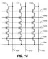
- FIG. 14shows a circuit diagram corresponding to the circuit formed by the structure of FIGS. 12 and 13 .
- FIG. 3Ashows a cross-section of a portion of a substrate 320 , a dielectric layer 332 overlying substrate 320 and an opening 324 in dielectric layer 322 that extends to a surface 326 of substrate 320 .
- Opening 324has a width of X 3 and a height of Y 3 .
- the aspect ratio of opening 324is Y 3 /X 3 .
- FIG. 3Bshows a cross-section of substrate 320 and dielectric layer 322 after deposition of a first conductive material to form first conductive portion 328 in opening 324 .
- First conductive materialis deposited in opening 324 to a thickness of Y 4 .
- First conductive materialis generally also deposited on top surface 330 of the dielectric layer 322 during this deposition, though material on top surface 330 may subsequently be removed. Some of the first conductive material may also deposit on sidewalls of opening 324 , though this is not shown in FIG. 3B .
- a material used as first conductive materialmay be chosen to provide good, void-free deposition in high aspect ratio openings even though it may have higher resistivity than other materials.
- first conductive materialmay be chosen to have adequate filling characteristics for an opening having aspect ratio Y 3 /X 3 .
- Doped polysilicon deposited using Low Pressure Chemical Vapor Deposition (LPCVD) or other meansis an example of such a material.
- LPCVDLow Pressure Chemical Vapor Deposition
- opening 324is filled to a height of Y 4 , leaving a depth of Y 5 still unfilled.
- unfilled portion 325 of opening 324has an aspect ratio of Y 5 /X 3 after deposition of first conductive material.
- Aspect ratio Y 5 /X 3is less than the original aspect ratio of Y 3 /X 3 .
- FIG. 3Cshows a cross-section after deposition of a second conductive material to form second conductive portion 332 in the unfilled portion 325 of opening 324 .
- the second conductive materialmay be chosen for its electrical properties such as low resistivity.
- the second conductive materialhas lower resistivity than the first conductive material.
- the second conductive materialmay have poorer filling characteristics than the first conductive material.
- second conductive materialmay be a material that would not provide good, void free deposition if used alone to fill an opening having an aspect ratio Y 3 /X 3 .
- the second conductive materialhas good enough filling properties to fill unfilled portion 325 of the opening 324 after first conductive portion 328 is deposited, i.e.
- second conductive materialcan give good, void free deposition in an opening having an aspect ratio of Y 5 /X 3 .
- the second conductive materialmay be a metal, for example a refractory metal such as tungsten or some other metal such as aluminum.
- First conductive portion 328 and second conductive portion 332together form a composite plug 334 that fills opening 324 .
- Composite plug 334 formed by first conductive portion 328 and second conductive portion 332has lower resistance than would be provided by a plug of similar dimensions formed by the first conductive material alone. Unlike a plug formed of the second conductive material alone, composite plug 334 does not suffer from voids. Thus, there are significant advantages over plugs formed from a single material.
- opening 324 as shown FIGS. 3A-3Chas smooth vertical sides
- real openingsmay have irregular sides and may not be vertical.
- the different layersmay have different etching characteristics causing some layers to be etched back further than others.
- An overhangmay be formed where a layer is etched less than the layer below it. Such irregularities make filling an opening more difficult.
- Plugsare generally used to connect to either end of a string of memory cells in such memories.
- a stringis formed by a series of floating gate cells connected by doped regions of the substrate.
- FIG. 4shows a cross-section of an exemplary NAND string 440 at an intermediate stage of memory array fabrication.
- Four floating gate memory cellsare formed by four control gates 442 a - 442 d , overlying four floating gates 444 a - 444 d , with floating gates 444 a - 444 d overlying channel regions 446 a - 446 d .
- Source and drain regions 448 a - 448 gare shown in the substrate connecting memory cells together to form the string.
- a first select gate 450is shown near one end of string 440 .
- First select gate 450consists of two parts 450 a and 450 b corresponding to floating gate and control gate layers respectively. Parts 450 a , 450 b are electrically connected together.
- First select gate 450may be considered the drain select gate.
- a second select gate 452is shown near the other end of NAND string 440 .
- Second select gate 452may be considered to be a source select gate.
- Second select gate 452consists of two parts 452 a and 452 b corresponding to floating gate and control gate layers respectively. Parts 452 a , 452 b are electrically connected together. However, select gates are not floating, but are connected by select lines extending across the array. In an alternative arrangement, a select gate may be formed by a single conductive portion. Select gates 450 , 452 are used to control the voltage applied to the memory cells of NAND string 440 .
- a dielectric layer 454covers floating gates 444 a - 444 d , control gates 442 a - 442 d and select gates 450 , 452 and the underlying substrate 456 .
- Dielectric layer 454may consist of a single material or two or more layers of different dielectric materials, which may be deposited at different times during the formation of NAND string 440 .
- Dielectric layer 452may be considered a single body for electrical purposes, providing isolation for NAND string 440 .
- a typical material used to form a dielectric layeris Boro-Phospho-Silicate Glass (BPSG).
- BPSGBoro-Phospho-Silicate Glass
- a dielectric layeris comprised of approximately 2500 Angstroms of BPSG overlying approximately 500 Angstroms of Silicon Nitride (SiN).
- FIG. 5shows NAND string 440 of FIG. 4 after formation of openings 560 , 562 in dielectric layer 454 .
- Openings 560 , 562are formed at either end of NAND string 440 at locations adjacent to source select gate 452 and drain select gate 450 .
- Openings 560 , 562may be formed by providing a patterned mask layer over dielectric layer 454 , the mask layer having openings that are aligned to the desired locations of openings in dielectric layer 454 .
- An anisotropic etchis then used to remove dielectric in the pattern established by the mask layer.
- Anisotropic etchingmay be Reactive Ion Etching (RIE) or another technique.
- Openings 560 , 562are formed so that they extend all the way to the surface of substrate 456 .
- impuritiesmay be introduced into the exposed portion of the substrate.
- N-type impuritiessuch as Arsenic or Phosphorous are implanted to lower the resistivity of implanted regions 564 , 566 of substrate 456 .
- impuritiesmay be diffused.
- P-type impuritiessuch as Boron may also be used in some cases. In some examples, no impurities are introduced at this point.
- doped polysiliconmay be deposited in openings 560 , 562 and some dopant from the polysilicon diffuses into the region below the opening to provide a sufficient doping level in this area. Even where doped polysilicon is not used, implantation of dopants may not always be necessary.
- Tungstenis commonly used to fill openings and form plugs to contact a substrate. Tungsten has low resistivity allowing the formation of low resistance structures and is also capable of withstanding subsequent high temperature processing. However, in some designs, particularly newer designs with smaller features, the aspect ratio of the openings may be too high to form good plugs using Tungsten. Doped polysilicon is another conductive material that may be used to fill openings and form plugs. Polysilicon deposited by LPCVD generally forms good, void-free plugs even where openings have high aspect ratios. However, polysilicon has a higher resistivity than Tungsten, so polysilicon structures have higher resistance than similar Tungsten structures. To overcome these limitations, a composite plug is formed of polysilicon and Tungsten deposited in sequence.
- FIG. 6shows NAND string 440 of FIG. 5 after deposition of a first conductive material in openings 560 , 562 and across the surface of dielectric layer 454 .
- the first conductive materialforms conductive portions 670 , 672 in openings 560 , 562 and forms first conductive layer 674 on dielectric layer 454 .
- the first conductive materialis polysilicon in this example, though other materials may also be used. Polysilicon may be deposited in a furnace or by other suitable means. Polysilicon is doped so that it has a low resistivity. Polysilicon may be deposited so that it directly overlies substrate 456 in openings 560 , 562 .
- a clean stepmay be performed prior to deposition of polysilicon to remove any native oxide or other material present on substrate 456 in openings 560 , 562 .
- Deposition of polysiliconis stopped before openings 560 , 562 are filled with polysilicon.
- Polysilicon depositionmay be stopped when the thickness of first conductive portions 670 , 672 in openings 560 , 562 has reached a predetermined thickness. The predetermined thickness can be calculated so that remaining unfilled portions 676 , 678 of openings 560 , 562 have aspect ratios that allow them, to be adequately filled by tungsten.
- FIG. 7shows NAND string 440 of FIG. 6 after deposition of a second conductive material to form second conductive layer 780 .
- the second conductive materialis Tungsten in this example, though other materials may also be used.
- the second conductive materialfills the unfilled portions 676 , 678 of openings 560 , 562 and extends across the first conductive layer 674 .
- a barrier layerPrior to deposition of Tungsten, a barrier layer (not shown) may be deposited.
- the barrier layermay be a composite layer, consisting of Titanium and Titanium Nitride (Ti/TiN) deposited in sequence.
- the second conductive materialmay be deposited directly on the first conductive material or a different barrier layer may lie between the first conductive material and the second conductive material.
- FIG. 8shows NAND string 440 of FIG. 7 after removal of excess first and second conductive material.
- First conductive layer 674is removed and second conductive layer 780 deposited over first conductive layer 674 is removed to the level of the top of dielectric layer 454 , leaving second conductive portions 882 , 884 .
- First and second conductive materialmay be removed by Chemical Mechanical Polishing (CMP) or by etching back or other means.
- CMPChemical Mechanical Polishing
- Remaining first conductive portions 670 , 672 and second conductive portions 882 , 884form plugs 886 , 888 .
- Plugs 886 , 888have lower resistance than would be provided by plugs of polysilicon alone.
- Plugs 886 , 888are also void-free even though openings 560 , 562 may have a higher aspect ratio than could normally be filled by Tungsten alone.
- FIG. 9shows NAND string 440 of FIG. 8 after deposition of a second dielectric layer 990 overlying first dielectric layer 454 and second conductive portions 882 , 884 .
- Second dielectric layer 990 of this exampleis a Silicon Dioxide (SiO 2 ) layer, formed by Chemical Vapor Deposition (CVD) using Tetraethyl Orthosilicate, Si(OC 2 H 5 ) 4 (TEOS). Other dielectric materials may also be used.
- FIG. 10shows NAND string 440 of FIG. 9 after patterning of second dielectric layer 990 .
- An opening 992is formed in second dielectric layer 990 over second conductive portion 882 . Opening 992 has roughly the same lateral dimensions as second conductive portion 882 .
- An opening 994is also formed in second dielectric layer 990 over second conductive portion 884 . However, opening 994 extends wider than second conductive portion 884 along the direction of NAND string 440 as shown in FIG. 10 . In addition, opening 994 extends in a direction perpendicular to the cross-section shown in FIG. 10 so that it overlies plugs of multiple strings. Openings 992 , 994 are formed by a single process using a single mask that is aligned so that openings 992 , 994 are positioned over second conductive portions 882 , 884 .
- FIG. 11shows NAND string 440 of FIG. 10 after deposition and planarization of a third conductive layer to form conductive portions 1102 , 1104 .
- conductive portions 1102 , 1104are formed of the same material as second conductive portions 882 , 884 (in this example—Tungsten).
- Drain plug 886is extended in the vertical direction as a result of this step.
- Source plug 888is connected by this step to other source contact plugs of other strings (not shown in FIG. 11 ) by conductive portion 1104 .
- FIG. 12shows NAND string 440 of FIG. 11 after subsequent formation of a third dielectric layer 1210 , a bitline 1212 and an additional conductive portion 1214 connecting drain plug 886 to bitline 1212 .
- Third dielectric layer 1210may be formed of Silicon Dioxide (SiO 2 ).
- Third dielectric layer 1210may be formed by High Density Plasma (HDP), plasma enhanced deposition, using TEOS or in some other manner.
- Additional conductive portion 1214may be Aluminum, Copper, Tungsten or other suitable conductive material.
- Bitline 1212is generally formed of a conductive material such as Aluminum or Tungsten.
- the combination of drain plug 886 and additional conductive portion 1214 that together connect one end of the NAND string 440 to bitline 1212may be referred to as a “bitline contact.”
- FIG. 13shows a top-down view of NAND string 440 of FIG. 12 and shows additional NAND strings 1320 , 1322 . While three strings 440 , 1320 , 1322 of four floating gate cells each are shown, actual memory arrays may have 8, 16, 32 or more floating gate cells in a string and thousands of strings may extend in two dimensions across a substrate. Individual strings 440 , 1320 , 1322 are separated by STI regions 1324 a - 1324 d that extend on either side of strings 440 , 1320 , 1324 .
- Wordlines 1326 a - 1326 d(indicated by broken lines) overlie floating gates of different strings forming control gates (for example, control gates 442 a - 442 d of NAND string 440 ) where they overlie floating gates.
- Source/drain implanted regions(for example source/drain implanted regions 448 a - 448 g of NAND string 440 ) in substrate 456 are shared by adjacent memory cells and provide electrical connection between memory cells of a NAND string.
- Select lines 1328 , 1330extend parallel to wordlines 1326 a - 1326 d across strings 440 , 1320 , 1322 , forming select gates (such as select gates 450 , 452 of NAND string 440 ) where they overlie channel regions of NAND strings.
- Plugs 886 , 888 of NAND string 440are shown in top-down view extending from implanted regions at either end of NAND string 440 .
- Source contact plugs 888 , 1332 , 1334 of NAND strings 440 , 1320 , 1322are shown connected together by conductive portion 1104 (common source line) formed as shown in FIG. 11 .
- Common source line 1104extends parallel to wordlines 1326 a - 1326 d and select lines 1328 , 1330 .
- FIG. 14shows a circuit diagram for NAND strings 440 , 1320 , 1322 of FIG. 13 .
- FIG. 14shows bitlines 1212 , 1450 , 1452 (not shown in FIG. 13 ) extending in the same direction as NAND strings 440 , 1320 , 1322 .
- Bitlines 1212 , 1450 , 1452are formed over strings 440 , 1320 , 1322 respectively, as shown in cross-section in FIG. 12 .
Landscapes
- Engineering & Computer Science (AREA)
- Physics & Mathematics (AREA)
- Condensed Matter Physics & Semiconductors (AREA)
- General Physics & Mathematics (AREA)
- Manufacturing & Machinery (AREA)
- Computer Hardware Design (AREA)
- Microelectronics & Electronic Packaging (AREA)
- Power Engineering (AREA)
- Semiconductor Memories (AREA)
- Non-Volatile Memory (AREA)
Abstract
Description
Claims (18)
Priority Applications (4)
| Application Number | Priority Date | Filing Date | Title |
|---|---|---|---|
| US11/296,235US7737483B2 (en) | 2005-12-06 | 2005-12-06 | Low resistance void-free contacts |
| PCT/US2006/061351WO2007067860A2 (en) | 2005-12-06 | 2006-11-29 | Low- resistance void-free contacts for eeprom devices |
| EP06848514AEP1958252A2 (en) | 2005-12-06 | 2006-11-29 | Low-resistance void-free contacts for eeprom devices |
| TW095145418ATWI332252B (en) | 2005-12-06 | 2006-12-06 | Low resistance void-free contacts |
Applications Claiming Priority (1)
| Application Number | Priority Date | Filing Date | Title |
|---|---|---|---|
| US11/296,235US7737483B2 (en) | 2005-12-06 | 2005-12-06 | Low resistance void-free contacts |
Publications (2)
| Publication Number | Publication Date |
|---|---|
| US20070126028A1 US20070126028A1 (en) | 2007-06-07 |
| US7737483B2true US7737483B2 (en) | 2010-06-15 |
Family
ID=38117833
Family Applications (1)
| Application Number | Title | Priority Date | Filing Date |
|---|---|---|---|
| US11/296,235Expired - Fee RelatedUS7737483B2 (en) | 2005-12-06 | 2005-12-06 | Low resistance void-free contacts |
Country Status (1)
| Country | Link |
|---|---|
| US (1) | US7737483B2 (en) |
Cited By (1)
| Publication number | Priority date | Publication date | Assignee | Title |
|---|---|---|---|---|
| US20110278658A1 (en)* | 2007-05-14 | 2011-11-17 | Kabushiki Kaisha Toshiba | Non-volatile semiconductor memory device and method of manufacturing the same |
Families Citing this family (8)
| Publication number | Priority date | Publication date | Assignee | Title |
|---|---|---|---|---|
| US7615448B2 (en)* | 2005-12-06 | 2009-11-10 | Sandisk Corporation | Method of forming low resistance void-free contacts |
| US7737483B2 (en) | 2005-12-06 | 2010-06-15 | Sandisk Corporation | Low resistance void-free contacts |
| US20090302472A1 (en) | 2008-06-05 | 2009-12-10 | Samsung Electronics Co., Ltd. | Non-volatile memory devices including shared bit lines and methods of fabricating the same |
| KR101166613B1 (en)* | 2009-06-08 | 2012-07-18 | 에스케이하이닉스 주식회사 | non-volatile memory device and manufacturing method thereof |
| US9406621B2 (en)* | 2010-06-10 | 2016-08-02 | Texas Instruments Incorporated | Ultraviolet energy shield for non-volatile charge storage memory |
| US8278203B2 (en) | 2010-07-28 | 2012-10-02 | Sandisk Technologies Inc. | Metal control gate formation in non-volatile storage |
| CN103928390B (en)* | 2013-01-10 | 2016-10-05 | 中芯国际集成电路制造(上海)有限公司 | The manufacture method of interconnection structure |
| CN115988881A (en)* | 2022-12-30 | 2023-04-18 | 东芯半导体股份有限公司 | NAND flash memory and its manufacturing method |
Citations (44)
| Publication number | Priority date | Publication date | Assignee | Title |
|---|---|---|---|---|
| US4203158A (en)* | 1978-02-24 | 1980-05-13 | Intel Corporation | Electrically programmable and erasable MOS floating gate memory device employing tunneling and method of fabricating same |
| US5043940A (en) | 1988-06-08 | 1991-08-27 | Eliyahou Harari | Flash EEPROM memory systems having multistate storage cells |
| US5070032A (en) | 1989-03-15 | 1991-12-03 | Sundisk Corporation | Method of making dense flash eeprom semiconductor memory structures |
| US5095344A (en) | 1988-06-08 | 1992-03-10 | Eliyahou Harari | Highly compact eprom and flash eeprom devices |
| US5172338A (en) | 1989-04-13 | 1992-12-15 | Sundisk Corporation | Multi-state EEprom read and write circuits and techniques |
| US5313421A (en) | 1992-01-14 | 1994-05-17 | Sundisk Corporation | EEPROM with split gate source side injection |
| US5315541A (en) | 1992-07-24 | 1994-05-24 | Sundisk Corporation | Segmented column memory array |
| US5343063A (en) | 1990-12-18 | 1994-08-30 | Sundisk Corporation | Dense vertical programmable read only memory cell structure and processes for making them |
| US5570315A (en) | 1993-09-21 | 1996-10-29 | Kabushiki Kaisha Toshiba | Multi-state EEPROM having write-verify control circuit |
| US5612254A (en)* | 1992-06-29 | 1997-03-18 | Intel Corporation | Methods of forming an interconnect on a semiconductor substrate |
| US5661053A (en) | 1994-05-25 | 1997-08-26 | Sandisk Corporation | Method of making dense flash EEPROM cell array and peripheral supporting circuits formed in deposited field oxide with the use of spacers |
| US5667219A (en) | 1993-12-24 | 1997-09-16 | Universal Sales Co., Inc. Ltd. | Variable display gaming machine |
| US5774397A (en)* | 1993-06-29 | 1998-06-30 | Kabushiki Kaisha Toshiba | Non-volatile semiconductor memory device and method of programming a non-volatile memory cell to a predetermined state |
| JPH10223867A (en) | 1997-02-10 | 1998-08-21 | Toshiba Corp | Semiconductor device and manufacturing method thereof |
| US5990004A (en) | 1998-07-15 | 1999-11-23 | United Microelectronics Corp. | Method for forming a tungsten plug and a barrier layer in a contact of high aspect ratio |
| US6046935A (en)* | 1996-03-18 | 2000-04-04 | Kabushiki Kaisha Toshiba | Semiconductor device and memory system |
| US6057193A (en)* | 1998-04-16 | 2000-05-02 | Advanced Micro Devices, Inc. | Elimination of poly cap for easy poly1 contact for NAND product |
| US6222762B1 (en) | 1992-01-14 | 2001-04-24 | Sandisk Corporation | Multi-state memory |
| US6310374B1 (en)* | 1997-12-25 | 2001-10-30 | Kabushiki Kaisha Toshiba | Nonvolatile semiconductor memory device having extracting electrode |
| US20020061645A1 (en) | 2000-04-13 | 2002-05-23 | Trivedi Jigish D. | Dual damascene interconnect |
| US6455424B1 (en) | 2000-08-07 | 2002-09-24 | Micron Technology, Inc. | Selective cap layers over recessed polysilicon plugs |
| US6512262B2 (en)* | 1997-06-06 | 2003-01-28 | Kabushiki Kaisha Toshiba | Non-volatile semiconductor memory device and method of manufacturing the same |
| US6522580B2 (en)* | 2001-06-27 | 2003-02-18 | Sandisk Corporation | Operating techniques for reducing effects of coupling between storage elements of a non-volatile memory operated in multiple data states |
| US20030098509A1 (en) | 1999-09-27 | 2003-05-29 | Kabushiki Kaisha Toshiba | Semiconductor device, semiconductor element and method for producing same |
| US20030111732A1 (en) | 2001-12-13 | 2003-06-19 | Akira Goda | Superconductor device and method of manufacturing the same |
| US6583479B1 (en)* | 2000-10-16 | 2003-06-24 | Advanced Micro Devices, Inc. | Sidewall NROM and method of manufacture thereof for non-volatile memory cells |
| TW546777B (en) | 2002-09-12 | 2003-08-11 | Promos Technologies Inc | Trench and via structure and filling method of the same |
| US20040161881A1 (en)* | 2001-01-11 | 2004-08-19 | Samsung Electronics Co., Ltd. | Semiconductor device and method of manufacturing the same |
| US6797570B2 (en)* | 2000-01-17 | 2004-09-28 | Samsung Electronics Co., Ltd. | NAND-type flash memory devices and methods of fabricating the same |
| TW200509257A (en) | 2003-06-04 | 2005-03-01 | Applied Materials Inc | HDP-CVD multistep gapfill process |
| US6888755B2 (en) | 2002-10-28 | 2005-05-03 | Sandisk Corporation | Flash memory cell arrays having dual control gates per memory cell charge storage element |
| EP1530237A2 (en) | 2003-11-10 | 2005-05-11 | Kabushiki Kaisha Toshiba | Nonvolatile semiconductor memory |
| US6925007B2 (en) | 2001-10-31 | 2005-08-02 | Sandisk Corporation | Multi-state non-volatile integrated circuit memory systems that employ dielectric storage elements |
| US6930001B2 (en)* | 2003-12-05 | 2005-08-16 | Hynix Semiconductor Inc. | Method for manufacturing NAND flash device |
| US20050266678A1 (en) | 2004-05-27 | 2005-12-01 | Micron Technology, Inc. | Source lines for NAND memory devices |
| US20050281092A1 (en)* | 2003-10-23 | 2005-12-22 | Micron Technology, Inc. | Nand memory arrays |
| US20050285148A1 (en) | 2003-11-17 | 2005-12-29 | Micron Technology, Inc. | Memory with polysilicon local interconnects |
| US20060001073A1 (en)* | 2003-05-21 | 2006-01-05 | Jian Chen | Use of voids between elements in semiconductor structures for isolation |
| US20060152644A1 (en)* | 2005-01-07 | 2006-07-13 | Samsung Electronics Co., Ltd. | Thin film transistor array panel |
| US20060223279A1 (en)* | 2005-04-01 | 2006-10-05 | Micron Technology, Inc. | Methods of forming trench isolation in the fabrication of integrated circuitry and methods of fabricating integrated circuitry |
| US7183153B2 (en)* | 2004-03-12 | 2007-02-27 | Sandisk Corporation | Method of manufacturing self aligned non-volatile memory cells |
| US20070087504A1 (en)* | 2005-10-18 | 2007-04-19 | Pham Tuan D | Integration process flow for flash devices with low gap fill aspect ratio |
| US20070126028A1 (en) | 2005-12-06 | 2007-06-07 | Masaaki Higashitani | Low resistance void-free contacts |
| US20070128787A1 (en) | 2005-12-06 | 2007-06-07 | Masaaki Higashitani | Method of forming low resistance void-free contacts |
- 2005
- 2005-12-06USUS11/296,235patent/US7737483B2/ennot_activeExpired - Fee Related
Patent Citations (49)
| Publication number | Priority date | Publication date | Assignee | Title |
|---|---|---|---|---|
| US4203158B1 (en)* | 1978-02-24 | 1992-09-22 | Intel Corp | |
| US4203158A (en)* | 1978-02-24 | 1980-05-13 | Intel Corporation | Electrically programmable and erasable MOS floating gate memory device employing tunneling and method of fabricating same |
| US5043940A (en) | 1988-06-08 | 1991-08-27 | Eliyahou Harari | Flash EEPROM memory systems having multistate storage cells |
| US5095344A (en) | 1988-06-08 | 1992-03-10 | Eliyahou Harari | Highly compact eprom and flash eeprom devices |
| US5070032A (en) | 1989-03-15 | 1991-12-03 | Sundisk Corporation | Method of making dense flash eeprom semiconductor memory structures |
| US5172338B1 (en) | 1989-04-13 | 1997-07-08 | Sandisk Corp | Multi-state eeprom read and write circuits and techniques |
| US5172338A (en) | 1989-04-13 | 1992-12-15 | Sundisk Corporation | Multi-state EEprom read and write circuits and techniques |
| US5343063A (en) | 1990-12-18 | 1994-08-30 | Sundisk Corporation | Dense vertical programmable read only memory cell structure and processes for making them |
| US5313421A (en) | 1992-01-14 | 1994-05-17 | Sundisk Corporation | EEPROM with split gate source side injection |
| US6222762B1 (en) | 1992-01-14 | 2001-04-24 | Sandisk Corporation | Multi-state memory |
| US5612254A (en)* | 1992-06-29 | 1997-03-18 | Intel Corporation | Methods of forming an interconnect on a semiconductor substrate |
| US5315541A (en) | 1992-07-24 | 1994-05-24 | Sundisk Corporation | Segmented column memory array |
| US5774397A (en)* | 1993-06-29 | 1998-06-30 | Kabushiki Kaisha Toshiba | Non-volatile semiconductor memory device and method of programming a non-volatile memory cell to a predetermined state |
| US5570315A (en) | 1993-09-21 | 1996-10-29 | Kabushiki Kaisha Toshiba | Multi-state EEPROM having write-verify control circuit |
| US5667219A (en) | 1993-12-24 | 1997-09-16 | Universal Sales Co., Inc. Ltd. | Variable display gaming machine |
| US5661053A (en) | 1994-05-25 | 1997-08-26 | Sandisk Corporation | Method of making dense flash EEPROM cell array and peripheral supporting circuits formed in deposited field oxide with the use of spacers |
| US6046935A (en)* | 1996-03-18 | 2000-04-04 | Kabushiki Kaisha Toshiba | Semiconductor device and memory system |
| US6160297A (en)* | 1997-02-10 | 2000-12-12 | Kabushiki Kaisha Toshiba | Semiconductor memory device having a first source line arranged between a memory cell string and bit lines in the direction crossing the bit lines and a second source line arranged in parallel to the bit lines |
| JPH10223867A (en) | 1997-02-10 | 1998-08-21 | Toshiba Corp | Semiconductor device and manufacturing method thereof |
| US6512262B2 (en)* | 1997-06-06 | 2003-01-28 | Kabushiki Kaisha Toshiba | Non-volatile semiconductor memory device and method of manufacturing the same |
| US6310374B1 (en)* | 1997-12-25 | 2001-10-30 | Kabushiki Kaisha Toshiba | Nonvolatile semiconductor memory device having extracting electrode |
| US6057193A (en)* | 1998-04-16 | 2000-05-02 | Advanced Micro Devices, Inc. | Elimination of poly cap for easy poly1 contact for NAND product |
| US5990004A (en) | 1998-07-15 | 1999-11-23 | United Microelectronics Corp. | Method for forming a tungsten plug and a barrier layer in a contact of high aspect ratio |
| US20030098509A1 (en) | 1999-09-27 | 2003-05-29 | Kabushiki Kaisha Toshiba | Semiconductor device, semiconductor element and method for producing same |
| US6797570B2 (en)* | 2000-01-17 | 2004-09-28 | Samsung Electronics Co., Ltd. | NAND-type flash memory devices and methods of fabricating the same |
| US20020061645A1 (en) | 2000-04-13 | 2002-05-23 | Trivedi Jigish D. | Dual damascene interconnect |
| US6455424B1 (en) | 2000-08-07 | 2002-09-24 | Micron Technology, Inc. | Selective cap layers over recessed polysilicon plugs |
| US6583479B1 (en)* | 2000-10-16 | 2003-06-24 | Advanced Micro Devices, Inc. | Sidewall NROM and method of manufacture thereof for non-volatile memory cells |
| US20040161881A1 (en)* | 2001-01-11 | 2004-08-19 | Samsung Electronics Co., Ltd. | Semiconductor device and method of manufacturing the same |
| US6522580B2 (en)* | 2001-06-27 | 2003-02-18 | Sandisk Corporation | Operating techniques for reducing effects of coupling between storage elements of a non-volatile memory operated in multiple data states |
| US6925007B2 (en) | 2001-10-31 | 2005-08-02 | Sandisk Corporation | Multi-state non-volatile integrated circuit memory systems that employ dielectric storage elements |
| US20030111732A1 (en) | 2001-12-13 | 2003-06-19 | Akira Goda | Superconductor device and method of manufacturing the same |
| TW546777B (en) | 2002-09-12 | 2003-08-11 | Promos Technologies Inc | Trench and via structure and filling method of the same |
| US6888755B2 (en) | 2002-10-28 | 2005-05-03 | Sandisk Corporation | Flash memory cell arrays having dual control gates per memory cell charge storage element |
| US7045849B2 (en)* | 2003-05-21 | 2006-05-16 | Sandisk Corporation | Use of voids between elements in semiconductor structures for isolation |
| US20060001073A1 (en)* | 2003-05-21 | 2006-01-05 | Jian Chen | Use of voids between elements in semiconductor structures for isolation |
| TW200509257A (en) | 2003-06-04 | 2005-03-01 | Applied Materials Inc | HDP-CVD multistep gapfill process |
| US20050281092A1 (en)* | 2003-10-23 | 2005-12-22 | Micron Technology, Inc. | Nand memory arrays |
| EP1530237A2 (en) | 2003-11-10 | 2005-05-11 | Kabushiki Kaisha Toshiba | Nonvolatile semiconductor memory |
| US20050285148A1 (en) | 2003-11-17 | 2005-12-29 | Micron Technology, Inc. | Memory with polysilicon local interconnects |
| US7115509B2 (en) | 2003-11-17 | 2006-10-03 | Micron Technology, Inc. | Method for forming polysilicon local interconnects |
| US6930001B2 (en)* | 2003-12-05 | 2005-08-16 | Hynix Semiconductor Inc. | Method for manufacturing NAND flash device |
| US7183153B2 (en)* | 2004-03-12 | 2007-02-27 | Sandisk Corporation | Method of manufacturing self aligned non-volatile memory cells |
| US20050266678A1 (en) | 2004-05-27 | 2005-12-01 | Micron Technology, Inc. | Source lines for NAND memory devices |
| US20060152644A1 (en)* | 2005-01-07 | 2006-07-13 | Samsung Electronics Co., Ltd. | Thin film transistor array panel |
| US20060223279A1 (en)* | 2005-04-01 | 2006-10-05 | Micron Technology, Inc. | Methods of forming trench isolation in the fabrication of integrated circuitry and methods of fabricating integrated circuitry |
| US20070087504A1 (en)* | 2005-10-18 | 2007-04-19 | Pham Tuan D | Integration process flow for flash devices with low gap fill aspect ratio |
| US20070126028A1 (en) | 2005-12-06 | 2007-06-07 | Masaaki Higashitani | Low resistance void-free contacts |
| US20070128787A1 (en) | 2005-12-06 | 2007-06-07 | Masaaki Higashitani | Method of forming low resistance void-free contacts |
Non-Patent Citations (9)
| Title |
|---|
| Final Office Action dated Sep. 16, 2008 in U.S. Appl. No. 11/296,022. |
| ISA/EPO, "Notification of Transmittal of the International Search Report and the Written Opinion of the International Searching Authority, or the Declaration," mailed on Jul. 10, 2007 in corresponding Int'l. App. No. PCT/US2006/061351, 13 pages. |
| Notice of Allowance and Fee(s) Due dated Sep. 11, 2009 in U.S. Appl. No. 11/296,022. |
| Office Action dated Mar. 6, 2009 in U.S. Appl. No. 11/296,022. |
| Office Action mailed Mar. 10, 2008, U.S. Appl. No. 11/296,022, filed Dec. 6, 2005. |
| Response to Office Action dated Nov. 7, 2008 in U.S. Appl. No. 11/296,022. |
| Response to Office Action filed Jun. 5, 2009 in U.S. Appl. No. 11/296,022. |
| Response to Office Action filed May 21, 2008, U.S. Appl. No. 11/296,022, filed Dec. 6, 2005. |
| Taiwanese Office Action dated Oct. 22, 2009 in Taiwanese Application No. 095145418. |
Cited By (4)
| Publication number | Priority date | Publication date | Assignee | Title |
|---|---|---|---|---|
| US20110278658A1 (en)* | 2007-05-14 | 2011-11-17 | Kabushiki Kaisha Toshiba | Non-volatile semiconductor memory device and method of manufacturing the same |
| US8399322B2 (en)* | 2007-05-14 | 2013-03-19 | Kabushiki Kaisha Toshiba | Non-volatile semiconductor memory device and method of manufacturing the same |
| US20130164929A1 (en)* | 2007-05-14 | 2013-06-27 | Kabushiki Kaisha Toshiba | Non-volatile semiconductor memory device and method of manufacturing the same |
| US8575017B2 (en)* | 2007-05-14 | 2013-11-05 | Kabushiki Kaisha Toshiba | Non-volatile semiconductor memory device and method of manufacturing the same |
Also Published As
| Publication number | Publication date |
|---|---|
| US20070126028A1 (en) | 2007-06-07 |
Similar Documents
| Publication | Publication Date | Title |
|---|---|---|
| US7183153B2 (en) | Method of manufacturing self aligned non-volatile memory cells | |
| US7795667B2 (en) | Semiconductor memory preventing an electric short circuit between a word line and a semiconductor substrate, and manufacturing method for the semiconductor memory | |
| KR100965112B1 (en) | Scalable self-aligning dual floating gate memory cell array and method for forming this array | |
| US6643186B2 (en) | Nonvolatile memory structures and fabrication methods | |
| US6953964B2 (en) | Non-volatile memory cell array having discontinuous source and drain diffusions contacted by continuous bit line conductors and methods of forming | |
| CN100405582C (en) | Charge trap memory device and manufacturing method thereof | |
| US7560766B2 (en) | Nonvolatile semiconductor memory | |
| US7615445B2 (en) | Methods of reducing coupling between floating gates in nonvolatile memory | |
| US7105406B2 (en) | Self aligned non-volatile memory cell and process for fabrication | |
| US7615448B2 (en) | Method of forming low resistance void-free contacts | |
| US7683422B2 (en) | Non-volatile memory devices with wraparound-shaped floating gate electrodes and methods of forming same | |
| US20070053223A1 (en) | Non-Volatile Memory Devices Having L-Shaped Floating Gate Electrodes and Methods of Forming Same | |
| US7375387B2 (en) | Method for producing semiconductor memory devices and integrated memory device | |
| US20090140313A1 (en) | Nonvolatile memory devices and methods of forming the same | |
| US7737483B2 (en) | Low resistance void-free contacts | |
| US20080074920A1 (en) | Nonvolatile Memory with Reduced Coupling Between Floating Gates | |
| WO2007067860A2 (en) | Low- resistance void-free contacts for eeprom devices | |
| US20080001211A1 (en) | Memory devices including spacer-shaped electrodes on pedestals and methods of manufacturing the same | |
| US8236646B2 (en) | Non-volatile memory manufacturing method using STI trench implantation | |
| US7060565B2 (en) | Fabrication of dielectric for a nonvolatile memory cell having multiple floating gates | |
| US20080272423A1 (en) | Conductive structures, non-volatile memory device including conductive structures and methods of manufacturing the same |
Legal Events
| Date | Code | Title | Description |
|---|---|---|---|
| AS | Assignment | Owner name:SANDISK CORPORATION, CALIFORNIA Free format text:ASSIGNMENT OF ASSIGNORS INTEREST;ASSIGNOR:HIGASHITANI, MASAAKI;REEL/FRAME:017320/0044 Effective date:20051201 Owner name:SANDISK CORPORATION,CALIFORNIA Free format text:ASSIGNMENT OF ASSIGNORS INTEREST;ASSIGNOR:HIGASHITANI, MASAAKI;REEL/FRAME:017320/0044 Effective date:20051201 | |
| STCF | Information on status: patent grant | Free format text:PATENTED CASE | |
| AS | Assignment | Owner name:SANDISK TECHNOLOGIES INC., TEXAS Free format text:ASSIGNMENT OF ASSIGNORS INTEREST;ASSIGNOR:SANDISK CORPORATION;REEL/FRAME:026369/0288 Effective date:20110404 | |
| FPAY | Fee payment | Year of fee payment:4 | |
| AS | Assignment | Owner name:SANDISK TECHNOLOGIES LLC, TEXAS Free format text:CHANGE OF NAME;ASSIGNOR:SANDISK TECHNOLOGIES INC;REEL/FRAME:038809/0472 Effective date:20160516 | |
| MAFP | Maintenance fee payment | Free format text:PAYMENT OF MAINTENANCE FEE, 8TH YEAR, LARGE ENTITY (ORIGINAL EVENT CODE: M1552) Year of fee payment:8 | |
| AS | Assignment | Owner name:WODEN TECHNOLOGIES INC., DELAWARE Free format text:ASSIGNMENT OF ASSIGNORS INTEREST;ASSIGNOR:SANDISK TECHNOLOGIES LLC;REEL/FRAME:058871/0928 Effective date:20210729 | |
| FEPP | Fee payment procedure | Free format text:MAINTENANCE FEE REMINDER MAILED (ORIGINAL EVENT CODE: REM.); ENTITY STATUS OF PATENT OWNER: LARGE ENTITY | |
| LAPS | Lapse for failure to pay maintenance fees | Free format text:PATENT EXPIRED FOR FAILURE TO PAY MAINTENANCE FEES (ORIGINAL EVENT CODE: EXP.); ENTITY STATUS OF PATENT OWNER: LARGE ENTITY | |
| STCH | Information on status: patent discontinuation | Free format text:PATENT EXPIRED DUE TO NONPAYMENT OF MAINTENANCE FEES UNDER 37 CFR 1.362 | |
| FP | Lapsed due to failure to pay maintenance fee | Effective date:20220615 |