US7737035B1 - Dual seal deposition process chamber and process - Google Patents
Dual seal deposition process chamber and processDownload PDFInfo
- Publication number
- US7737035B1 US7737035B1US11/542,723US54272306AUS7737035B1US 7737035 B1US7737035 B1US 7737035B1US 54272306 AUS54272306 AUS 54272306AUS 7737035 B1US7737035 B1US 7737035B1
- Authority
- US
- United States
- Prior art keywords
- seal
- deposition
- substrate
- volume
- station
- Prior art date
- Legal status (The legal status is an assumption and is not a legal conclusion. Google has not performed a legal analysis and makes no representation as to the accuracy of the status listed.)
- Active, expires
Links
Images


Classifications
- C—CHEMISTRY; METALLURGY
- C23—COATING METALLIC MATERIAL; COATING MATERIAL WITH METALLIC MATERIAL; CHEMICAL SURFACE TREATMENT; DIFFUSION TREATMENT OF METALLIC MATERIAL; COATING BY VACUUM EVAPORATION, BY SPUTTERING, BY ION IMPLANTATION OR BY CHEMICAL VAPOUR DEPOSITION, IN GENERAL; INHIBITING CORROSION OF METALLIC MATERIAL OR INCRUSTATION IN GENERAL
- C23C—COATING METALLIC MATERIAL; COATING MATERIAL WITH METALLIC MATERIAL; SURFACE TREATMENT OF METALLIC MATERIAL BY DIFFUSION INTO THE SURFACE, BY CHEMICAL CONVERSION OR SUBSTITUTION; COATING BY VACUUM EVAPORATION, BY SPUTTERING, BY ION IMPLANTATION OR BY CHEMICAL VAPOUR DEPOSITION, IN GENERAL
- C23C16/00—Chemical coating by decomposition of gaseous compounds, without leaving reaction products of surface material in the coating, i.e. chemical vapour deposition [CVD] processes
- C23C16/44—Chemical coating by decomposition of gaseous compounds, without leaving reaction products of surface material in the coating, i.e. chemical vapour deposition [CVD] processes characterised by the method of coating
- C23C16/4401—Means for minimising impurities, e.g. dust, moisture or residual gas, in the reaction chamber
- C23C16/4409—Means for minimising impurities, e.g. dust, moisture or residual gas, in the reaction chamber characterised by sealing means
Definitions
- This inventionpertains to apparatus and processes for conducting chemical depositions, and may find particular use in depositing a conformal film of dielectric material with a high degree of surface smoothness particularly suited to high aspect ratio gap fill applications in semiconductor device fabrication.
- Conformal, uniform dielectric filmshave many applications in semiconductor manufacturing.
- ICssub-micron integrated circuits
- several layers of dielectric filmare deposited.
- STIshallow trench isolation
- PMDpremetal dielectric
- IMDinter-metal dielectric
- ILDinterlayer dielectric
- Other applications of conformal dielectric filmsmay be as sacrificial or permanent spacer layers, sacrificial or permanent storage node separation layers, or as dielectric liners for through-wafer vias. All of these layers require silicon dioxide or other low dielectric constant films that fill features of various sizes and have uniform film thicknesses across the wafer.
- ALDatomic layer deposition
- ALD methodsinvolve self-limiting adsorption of reactant gases and can provide thin, conformal dielectric films within high aspect ratio features.
- the ALD processinvolves exposing a substrate to alternating doses of, usually two, reactant gases.
- reactants A and Bare first and second reactant gases for an ALD process, after A is adsorbed onto the substrate surface to form a saturated layer, B is introduced and reacts only with adsorbed A. In this manner, a very thin and conformal film can be deposited.
- One drawback, however, to ALDis that the deposition rates are very low. Films produced by ALD are also very thin (i.e., about one monolayer); therefore, numerous ALD cycles must be repeated to adequately fill a gap feature. These processes are unacceptably slow in some applications in the manufacturing environment.
- PDLpulsed deposition layer
- RVDrapid surface-catalyzed vapor deposition
- PDL-type processes for forming silicon-based dielectricscan use as reactant A a metal or metalloid catalyst (e.g., trimethylaluminum (TMA)) or metal and metalloid-free catalysts (e.g., an organic acid such as acetic acid (CH 3 COOH) or an inorganic acid such as phosphoric acid (H 3 PO 4 ); and as reactant B, a silicon-containing dielectric precursor.
- a metal or metalloid catalyste.g., trimethylaluminum (TMA)
- metal and metalloid-free catalystse.g., an organic acid such as acetic acid (CH 3 COOH) or an inorganic acid such as phosphoric acid (H 3 PO 4
- reactant Ba silicon-containing dielectric precursor.
- the first (catalytic) reagentcan be trimethylaluminum (TMA) and the second (silicon-containing) reagent can be tris t(pentoxy)silanol (TPOSL).
- a heated silicon substrateis first exposed to a dose of TMA, which is thought to react with the silicon surface to form a thin layer of surface-bound aluminum complex.
- TMAis pumped or flushed from the deposition chamber.
- a large dose of TPOSLis then introduced.
- the aluminum complexcatalyzes the conversion of the silanol to silicon oxide until the silanol is consumed, or the growing film covers or otherwise inactivates the catalytic complex.
- excess silanolis used, the film growth is usually self-limiting and a thick and uniform film results. Unreacted silanol is then removed from the chamber and the growth cycle repeated.
- a filmis often deposited on the chamber walls in addition to the desired location, on the substrate (e.g., silicon wafer) surface.
- this unwanted depositioncan occur as the precursors adsorb to the walls of the reactor in addition to the wafer surface and subsequently react to form film in later PDL/ALD steps.
- This filmcan build up on the chamber walls and can act as a source of chemical contaminants and particulates. It has been well documented for many CVD and ALD/PDL systems that a periodic cleaning of the chamber walls to remove these deposits is beneficial. If these chamber cleans are not performed, the film stresses may be so large that the film delaminates from the chamber wall, leading to particle deposition on the wafer surface. However, these chamber cleans reduce chamber productivity.
- the present inventionprovides an apparatus and method for sealing and unsealing a chemical deposition apparatus.
- the apparatusincludes a microvolume that has dual sealing elements at its periphery. One seal, the outer seal, is used to seal the inside of the volume from the main process chamber. The second (inner) seal is used to seal the inside of the microvolume from a vacuum source.
- the apparatus and process of the present inventionhas several advantages, including:
- the dual-seal arrangementincorporates the sealing function and mechanism into the wafer handling mechanism by using the pedestal and/or showerhead module motion to sequence and actuate at least part of the dual seal.
- the dual-seal arrangement of the inventionincorporates the sealing function and mechanism into the wafer handling mechanism by using the pedestal and/or showerhead module motion to sequence and actuate at least part of the dual seal.
- the dual-seal arrangementprovides the sealing point very near the wafer edge allowing minimal chamber volume and reducing or eliminating dead legs (area that is a dead end without fluid flow through; that can become a refuge for by-products or particles that are very difficult to remove by purging the chamber).
- a very small deposition chamber volume in the form of the microvolumes formed by engagement of the pedestal and showerhead modules and operation of the dual sealalso results in minimized chemical usage.
- the dual-seal arrangementprovides a sealing element concentric to the wafer. As such it can provide a concentric pumping or unsealing that can facilitate axis-symmetric flow to the wafer; symmetric flow during post-exposure microvolume evacuation preserves film uniformity.
- the dual-seal arrangementprovides a vacuum path from the microvolume when only the outer seal is engaged. This greatly facilitates station isolation in multi-station reactors by minimizing the amount of precursor exposure to the main process chamber and helps avoid the need for an in situ clean.
- elastomeric sealsto form the dual seal in various embodiments is mechanically simple, resulting in low cost and complexity of apparatus fabrication and operation, low maintenance and greater productivity.
- the inventionrelates to a chemical deposition process chamber apparatus.
- the apparatusincludes a substrate pedestal module comprising a substrate support region; a showerhead module comprising process fluid injection outlets; and a dual seal composed of one or more seal members comprised by either or both of the substrate pedestal module or the showerhead module, the one or more seal members operable to form a plurality of circumferential seals around a microvolume encompassing the substrate support region.
- the one or more sealsare operable to form an inner vacuum-tight seal separating a main process chamber from the inside of the microvolume and a vacuum source fluidly connected with the microvolume.
- the one or more sealsare operable to form an outer vacuum-tight seal separating the main process chamber from the inside of the microvolume and from the vacuum source.
- the dual sealmay be completely open so that there is no vacuum-tight separation of the substrate support region and the main process chamber.
- the one or more seal memberscomprise a pair of concentric elastomeric seals.
- the pair of concentric elastomeric sealscan be an inner O-ring circumscribed by an outer lip seal.
- the pair of concentric elastomeric sealscan be borne by the pedestal module, the showerhead module, or a combination.
- At least the inner O-ring sealcan be composed of a material that retains its elastomeric properties at a temperature between ⁇ 100° C. and 300° C., upon exposure to chemicals used in the deposition process, and with mechanical cycling (repeated sealing and unsealing); and has low or no particulate generation or chemical outgassing with mechanical cycling.
- An example of a suitable materialis a perfluoroelastomer.
- the perfluoroelastomermay include a filler a particulate filler, that may be a nano-particulate.
- Either or both of the pair of circumferential sealscan be engaged with one of the modules in a channel circumferential to the substrate support region and operable to engage with the other of the modules by contact to form a seal.
- an outer lip seal channelmay include a re-entrant feature on its lower outer sidewall that engages a tab on the lip seal.
- the upper inner side wall of the lip seal channelcan have a cut away to accommodate compression of the seal when it is engaged, particularly when the seal is fully closed.
- the one or more seal memberscan include a concentric elastomeric seal and a plurality of discrete vacuum channels and valves disposed concentrically about the elastomeric seal.
- the inner seal, between the vacuum source and the deposition region of the microvolumeis created by the plurality of discrete vacuum channels and valves, which may be located in the showerhead module.
- the outer seal, between the microvolume and the main reactor chamber,is formed by a concentric elastomeric seal, such as an O-ring.
- the one or more seal memberscan include a single elastomeric seal member mounted on a flexible element operable to engage each of the modules with a separate contact area to provide the plurality of circumferential seals defining the microvolume with (outer seal engaged only) and without (both inner and outer seals engaged) a fluid path to the vacuum source.
- the seal elementcan be composed of a suitable elastomeric material as described above with reference to the concentric elastomeric seals, and the flexible element can be a metal.
- the inventionin another aspect, relates to a multi deposition station system (MDSS) for chemical deposition processing having one or more stations with a chemical deposition process chamber apparatus as described above.
- MDSSmulti deposition station system
- the inventionin another aspect, relates to a method of conducting a chemical deposition process in a dual seal apparatus.
- the methodgenerally involves providing a deposition substrate to a substrate support region of a deposition chamber having a dual seal configuration as described herein.
- An outer circumferential sealdefining a volume encompassing the substrate support region and fluidly connected with an evacuation apparatus is formed.
- An inner circumferential seal that seals the substrate support region from the evacuation apparatus to form a deposition microvolumeis also made.
- a chemical depositionis conducted in the microvolume.
- the inner sealis then opened and the microvolume evacuated.
- the outer sealis then opened and the substrate is removed from the substrate support region, for example by indexing of wafers in a multiple deposition station system (MDSS).
- MDSSmultiple deposition station system
- the inner sealin order to avoid wafer floating and/or backstreaming, particularly where a plurality of deposition chambers having the dual seal apparatus described above are combined in a multi-station deposition system (MDSS) reactor in which the plurality of deposition chambers share a common vacuum foreline for the evacuation apparatus, the inner seal can be opened gradually. Gradual opening of the inner seal prevents a sudden pressure release that can cause wafer float and/or backstreaming of the gas flow from one chamber to another.
- MDSSmulti-station deposition system
- FIG. 1is a schematic cross-sectional diagram showing relevant basic features of a chemical deposition station in accordance with which the present invention can be implemented.
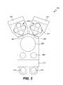
- FIG. 2is a schematic diagram showing relevant features of a single chamber, multi-station reactor system in accordance with which the present invention can be implemented.
- FIG. 3is a schematic diagram showing relevant features of a two-chamber multi-station process module incorporating two systems such as shown in FIG. 2 .
- FIGS. 4A-Cillustrate relevant features of the structure and operation of an embodiment of the present invention having two elastomeric seals located concentrically on the pedestal with their sealing positions offset in the vertical direction.
- FIG. 5illustrates an example of the embodiment described with reference to FIGS. 4A-C in further detail.
- FIG. 6shows a dual circumferential elastomeric seal embodiment as described with reference to FIGS. 4A-C and 5 with the elastomeric seals and their associated mounting features on the pedestal.
- FIG. 7illustrates an alternative embodiment of the invention in which a seal element that has sealing surfaces on its top and bottom surfaces and is mounted on a flexible element can be used to form inner and outer seals.
- FIGS. 8A-Billustrate in lateral and vertical cross-sections, respectively, another alternative implementation of the invention having a plurality of discrete valves arranged peripherally around the microvolume can be used in combination with a circumferential elastomeric seal to form the inner and outer seals of the dual seal, respectively.
- FIG. 9provides a process flow depicting steps in an example of a sealing and unsealing operation according to the present invention, consistent with the embodiment illustrated in FIGS. 4A-C .
- FIG. 10depicts a plot of pressure vs. time illustrating a representative smooth gradient profile of the gradual pressure release resulting from operation in accordance with the present invention, that avoids wafer floating and backstreaming.
- FIGS. 11A-Cillustrate sample unsealing methods in accordance with the present invention.
- the present inventionprovides an apparatus and associated method for conducting a chemical deposition.
- the apparatus and methodare particularly applicable to use in conjunction with a semiconductor fabrication based dielectric deposition process that requires separation of self-limiting deposition steps in a multi-step dielectric deposition process (e.g., atomic layer deposition (ALD) or pulsed deposition layer (PDL) processing for catalyst and silicon precursor deposition), however they are not so limited.
- ALDatomic layer deposition
- PDLpulsed deposition layer
- the apparatus and process of the inventionare described with reference to such PDL embodiments.
- a PDL processinvolves sequentially depositing a plurality of atomic-scale films on a substrate surface by sequentially exposing and removing reactants to and from the substrate surface.
- An exemplary case of PDL processing using reactant gases A and Bwill now be used to illustrate principle operations of a PDL process in accordance with the present invention.
- gas Ais injected into a chamber and the molecules of gas A are chemically or physically adsorbed to the surface of a substrate, thereby forming a “saturated layer” of A.
- Formation of a saturated layeris self-limiting in nature and represents a thermodynamically distinct state of adsorbed A on a surface. In some cases, a saturated layer is only one monolayer. In other cases, a saturated layer is a fraction of a monolayer, or some multiple of monolayers.
- the remaining gas A in the chamberis purged using an inert gas and/or pumped using a vacuum pump.
- the gas Bis injected so that it comes in contact with the adsorbed layer of A and reacts to form a reaction product of A and B. Because the saturated layer of A is thin and evenly distributed over the substrate surface, excellent film step coverage (i.e., conformal films) can be obtained. B is flowed over the substrate for a period of time sufficient to allow the reaction between A and B to preferably go to completion; i.e., all of the adsorbed A is consumed in the reaction.
- Bis flowed over the substrate for a period of time sufficient for a large enough quantity of B to be exposed to the substrate, resulting in a film formation in excess of one monolayer.
- the flow of Bis stopped. There may be an optional soak time after stopping the delivery of B, to allow enough time to fully complete the reaction. At this point, residual gas B and any byproducts of the reaction are purged and/or pumped from the chamber. Further PDL cycles of exposure to A, followed by exposure to B, can be implemented and repeated as needed for multiple layers of material to be deposited.
- ALDatomic layer deposition
- ALD and PDL methodsare related to the well-established chemical vapor deposition (CVD) techniques.
- CVDchemical vapor deposition
- the chemical reactant gasesare simultaneously introduced in a reaction chamber and allowed to mix and chemically react with each other in gas phase. The products of the mixed gases are then deposited on the substrate surface.
- ALD and PDL processing methodsdiffer from CVD since in ALD and PDL the chemical reactant gases are individually injected into a reaction chamber and not allowed to mix prior to contacting the substrate surface. That is, ALD and PDL are based on separated surface-controlled reactions.
- the precursorsare not put into the same deposition space (chamber or chamber region), they do not readily react to deposit and accumulate film on the walls of the chamber. Since there is little or no film growth on the chamber walls, the number of in situ plasma cleans required to keep the particle performance of the chamber within acceptable limits is minimized. This dramatically improves the availability of the tool for processing wafers.
- a multi-station arrangementis used.
- four stationseach having its own microvolume formed by engagement of separate pedestal and showerhead assemblies at each station, are provided within the main reactor process chamber.
- two of the stationsare used for exposure of catalyst (i.e., reactant A, e.g., TMA) to the substrate and two are used for exposure of a silicon-containing precursor (i.e., reactant B, e.g., TPOSL).
- catalysti.e., reactant A, e.g., TMA
- reactant Be.g., TPOSL
- a PDL process module in the reactordelivers process chemistry into each of the four microvolumes.
- the process pressurecan reach 20T or more for two of the microvolumes, and these microvolumes may share a common foreline.
- the chamberneeds to be unsealed and the gas evacuated. With throughput as a concern, the gas must be evacuated quickly when the microvolume is opened.
- sharp pressure changescan allow pressure differentials between the top and bottom surfaces of the wafer that can float the wafer; increasing the likelihood of particle generation, damage to the wafer and misalignment of the wafer with the wafer handling apparatus. This is particularly problematic due to the repeated process cycles that each wafer may see and the potential accumulation of effects of movement due to floating.
- these microvolumesmay not open exactly the same causing backstreaming of gas from one station (microvolume) to the other.
- microvolume sealing apparatus and methodsand improved control of microvolume unsealing and evacuation would be desirable.
- the present inventionprovides chemical deposition apparatus having a small volume chamber, the microvolume, that has dual sealing elements at its periphery.
- One sealthe outer seal, is used to seal the inside of the volume from the main process chamber, the second (inner) seal is used to seal the inside of the volume from a vacuum source.
- the inventionprovides a chemical deposition process chamber apparatus, comprising: a substrate pedestal module comprising substrate support region; a showerhead module comprising process fluid injection outlets; one or more seal members comprised by either or both of the substrate pedestal module or the showerhead module, the one or more seal members operable to engage either or both of the modules to provide a plurality of peripheral seals defining a greater volume and a lesser volume within the greater volume encompassing the substrate support region and exposed to the showerhead module process fluid injection outlets; and evacuation apparatus fluidly connected with the greater volume and not the lesser volume.
- the inventionallows a wafer to be transferred into a microvolume (i.e., a small chemical exposure chamber) while at vacuum.
- the microvolumecloses by engagement of the pedestal and showerhead modules and closure of inner and outer peripheral seals.
- the waferis exposed to a chemical in a stopped flow method (dose) at a specific delivery amount (generally measured in micro-moles) and for a specific time.
- dosea stopped flow method
- specific delivery amountgenerally measured in micro-moles
- the chemicalis then removed (purged) from the microvolume by opening the microvolume sufficiently to break the inner seal while the outer seal remains intact.
- a path to vacuumis opened when the inner seal is broken, allowing gas in the microvolume to evacuate.
- the outer sealcan then be broken and the microvolume opened to remove the wafer without releasing appreciable amounts of the chemical into the main process chamber.
- FIG. 1is a schematic cross-sectional diagram showing relevant basic features of a chemical deposition station in accordance with which the present invention can be implemented.
- the station 100has a vacuum/flow environment around a region 102 where the deposition substrate (e.g., wafer) 101 is positioned during exposure to chemical reactants that is within but separate from the main reactor volume 107 .
- This region 102is defined by walls composed of the inner surfaces of a module that supports the substrate and a module that provides the chemical reactants, and is referred to herein as a “microvolume” 102 .
- Thisis generally accomplished by having the wafer 101 on a moving pedestal module 103 that can be raised or lowered relative to a showerhead module 121 to either close or open the station.
- the stationis can be opened or closed by raising or lowering the showerhead module 121 or by movement of both the pedestal and the showerhead modules.
- a hinged configurationis also possible. While closed, there can be a separate flow of precursors to, and a separate vacuum evacuation from, the deposition region, the microvolume 102 .
- Precursorsare introduced into the microvolume via lines, represented by 109 .
- Each linemay have a corresponding accumulator 115 , and can be isolated from the microvolume using isolation valves 113 .
- the apparatusmay be modified to have one or several more lines along with corresponding isolation valves and accumulators, depending on the number of precursors used.
- the microvolume 102is evacuated through vacuum lines, represented by 117 , that are connected to a vacuum source, such as a vacuum pump, and can be isolated from the microvolume using an isolation valve 118 .
- a vacuum line 117 from another stationmay share a common foreline 119 with the vacuum line 117 .
- precursor delivery linesmay be shared between multiple stations.
- a hot wall in the showerhead module 121which is capable of producing temperatures greater than room temperature, is used to maintain the proper temperature inside the enclosure.
- the showerhead wallscan be heated to greater than 250° C., and/or the pedestal can be heated to greater than 250° C.
- the station 100includes a seal 105 at the point of engagement of the pedestal 103 and showerhead 121 modules.
- the sealis a dual seal and generally includes at least one circumferential elastomeric seal portion.
- the circumferential elastomeric seal(s)should be composed of a material with thermal and chemical stability to the temperatures and reactants in the operating environment of the reactor. For example, in various implementations, the material would normally be subjected to temperatures ranging from about ⁇ 100 to 300° C., although stability over a subset of this full range will be adequate for most applications.
- the materialshould also have adequate resistance to mechanical cycling to be able to retain its elastomeric sealing and other important properties through repeated opening and closing of the microvolume. In addition, the material should generate few or no particulates in the course of reactor operations and should have little or no chemical outgassing. Suitable materials for preferred implementations include prefluoroelastomers. Examples include KALREZ, available from DuPont and G-67P, available from Perlast. The latter is a nano-filled perfluoroelastomer that is particularly preferred in many applications.
- the desired properties of the elastomeric materialmay be more applicable to one of the seals than the other, as will be discussed further below, and VITON may also be used as a seal material.
- An advantage of this configurationis that the total volume inside the station 100 is much smaller than the main reactor volume. For example, using a 2-3 mm gap between the wafer and the lower surface of the showerhead and a 300 mm wafer, the total volume of the station may be less than about 0.25 L.
- FIG. 2is a schematic diagram showing relevant features of a single chamber, multi-station reactor system in accordance with which the present invention can be implemented.
- Four stations 201are contained within a single main reactor chamber vacuum enclosure 200 with a single robotic spindle mechanism 203 for moving wafers 205 between stations.
- some stationsare used to apply a catalytic precursor only, such as TMA, and some stations are used to apply a silicon-containing precursor.
- Some or all of the stationscan have a dual seal configuration and operation in accordance with the present invention.
- the stationsare used to apply the silicon-containing precursor have the dual seal configuration, while the stations used to apply the catalytic reactant can have a single seal configuration.
- Each station deposition microvolumeas described basically above, and in more detail with respect to specific embodiments below, is isolated from other stations by seals.
- the number of stations in a particular reactorwill depend upon available space, but typically the number of each kind of station is a multiple of the number of reactants used in the process. As an example, if two reactants are used, then there may be two, four or six stations (for instance, four: two of reactant A and two of reactant B). If three reactants are used, then there could be three or six stations (for instance, six: two of reactant A, two of reactant B, and two of reactant C).
- the order of running the wafers 205would be sequentially from a station running reactant A, then to B, then to C, etc., with a repetition of this cycle if there were more than one of each kind of station or by returning the wafers to the stations that had already been visited. In this way it is possible to accomplish the number of cycles that may be required to grow a film of a desired thickness without leaving the vacuum enclosure of the main reactor chamber 200 .
- reactant Bcan be run before reactant A; prior to any reactant exposure, the first step is can be a preheat step; and multiple doses of reactants A or B can be accommodated at each station before indexing to next station.
- An example of a multi-station reactor system suitable for conducting PDL-based dielectric gap fillis a four station reactor with two stations of reactant A (catalyst) and two stations of reactant B (silicon-containing).
- the wafer 205Upon entering the reactor, the wafer 205 is placed on the first station which would deposit reactant A. The wafer 205 is then moved by spindle mechanism 203 to station 2 , where reactant B is deposited. Wafer 205 is then moved to station 3 where a second layer of reactant A is deposited. The wafer is then moved to station four and a second layer of reactant B is deposited. At this point, the wafers are removed from vacuum enclosure 200 or, alternately, more layers of reactants A and B may be deposited until a desired film thickness is reached.
- FIG. 3is a schematic diagram showing relevant features of a two-chamber multi-station process module incorporating two systems 200 such as shown in FIG. 2 .
- Multi-station module 300is shown with process module 301 and process module 303 .
- Each process moduleis physically connected to wafer transfer mechanism 305 .
- Two vacuum-tight doors 307one for each chamber, separate process modules 301 and 303 from wafer transfer mechanism 305 .
- the pressure in the wafer transfer mechanismis kept slightly higher than that in each station. For example, a ⁇ P of about 0.2-0.7 Torr (e.g., 0.5) may be used.
- Vacuum pumps 309are used to maintain the proper level of vacuum in module 300 .
- a wafer handler 311is used to transfer wafers into wafer transfer mechanism 305 .
- Semiconductor wafersare supplied to the process module via wafer cassettes 313 .
- wafer cassettes 313also known as FOUPs: Front Opening Unified Pods
- Process modules 301 and 303are, in one embodiment of the invention, arranged as described with reference to FIG. 2 , with a four-station 317 reactor 200 per module.
- one stationis dedicated to exposure of the catalyst (e.g., aluminum-containing precursor), which may be trimethyl aluminum, while another station is dedicated to exposure of silanol or another silicon-containing precursor.
- the catalyste.g., aluminum-containing precursor
- the catalyste.g., aluminum-containing precursor
- another stationis dedicated to exposure of silanol or another silicon-containing precursor.
- Individual stationscan be constructed or lined with materials suitable for the processes that will be performed within each station, as will be understood by those of skill in the art.
- aluminummay be used as the principal material for fabrication of the chambers, reactors and apparatus described herein.
- the dual seal concept of the present inventioncan be implemented in several different ways.
- the dual sealsare actuated by pressing the pedestal against the showerhead. The motion of the pedestal sequences the seals to provide the desired process conditions.
- the dual seal actuationinvolves separate and/or additional mechanisms.
- FIGS. 4A-Cprovide illustrations showing relevant features of the structure and operation of such an embodiment of the invention.
- the first seal(outer seal, between the microvolume 410 and the main reactor chamber 420 ) is made when the pedestal 401 and the showerhead 403 modules come together and the higher vertically offset outer elastomeric seal 405 contacts a sealing surface 406 on the showerhead module 403 .
- the outer elastomeric sealis ideally maximally deformable and resistant to mechanical cycling while still able to retain the seal so that the cross-sectional area of the gap available for pumping during evacuation of the microvolume 410 , as illustrated in FIG. 4B below, can be maximized.
- a lip sealis one preferred configuration for the outer seal element.
- the second sealinner seal, between the vacuum source 430 and the deposition region of the microvolume 410
- the inner sealideally has chemical resistance to all reactants used in operation of the apparatus and does not generate particles during repeated sealing and unsealing operations.
- An O-ring sealis one preferred configuration for the inner seal element.
- FIG. 4Ashows the apparatus in the fully closed position with both seals engaged. This is the position during deposition.
- FIG. 4Bshows the apparatus in the half-closed position with the outer seal 405 closed but the inner seal 407 open. This is the position during evacuation of the residual deposition reactants following deposition.
- FIG. 4Cshows the apparatus in the open position with the both seals open. This is the position for transfer of the wafer 440 in or out of the station's microvolume 410 .
- one or both sealscan also be borne by the showerhead module, and the microvolume can be opened or closed by movement of either or both of those modules.
- FIG. 5illustrates an example of the embodiment described with reference to FIGS. 4A-C in further detail.
- the illustrated embodimenthas the dual circumferential elastomeric seals mounted on the pedestal. Other features are discussed above are labeled.
- the elastomeric seals and their associated mounting features on the pedestal, for example, modulehave a particular geometry.
- An example of this embodiment 600is shown in FIG. 6 .
- the mounting features for both sealsare circumferential channels 602 , 604 in the surface of the pedestal 606 that will engage with the showerhead module 608 to form the deposition microvolume.
- the channel 602 for the outer sealis configured with a reentrant feature 612 on the lower portion of its outer wall, and the outer elastomeric seal 614 is a lip seal configured with a corresponding tab 616 , so that the channel feature 612 and the tab 616 fit together in a lock-and-key manner.
- This configurationretains the elastomeric seal 614 in place, preventing it from popping out of the channel 602 when the lip seal is engaged.
- the upper portion of the inner wallcan also be configured to have a cut-away 618 to provide clearance for the elastomeric lip seal as it folds down when engaging the showerhead module to form the seal.
- the channel 604 for the inner seal in the illustrated embodimenthas a dovetail shape that holds an elastomeric O-ring inner seal element 620 in place.
- FIG. 7illustrates an alternative embodiment 700 of the invention in which a seal element 702 that has sealing surfaces on its top 704 and bottom surfaces 706 and is mounted on a flexible element 708 can be used to form the inner and outer seals.
- the flexible element 708which may be metal, plastic or another suitable material, is mounted to the showerhead module 710 . This design allows the first seal (outer seal, between the microvolume and the main reactor chamber) to be made when the pedestal 712 contacts the bottom surface 706 of the sealing element 710 .
- the second sealis made when the pedestal travel (and/or travel of the showerhead module relative to the pedestal) deflects the flexible element 708 allowing the top surface 704 of the seal element to contact the showerhead 710 , sealing off the vacuum source 714 .
- the latter (fully closed) position of the seal and flexible elementsis represented by the broken line 715 in the figure. Given these specifications, one of skill in the art could readily determine an alternate configuration based on the principles of this embodiment, but with the flexible seal element mounted on the pedestal module.
- a plurality of discrete valves arranged peripherally around the microvolumecan be used in combination with a circumferential elastomeric seal to form the inner and outer seals of the dual seal, respectively.
- the inner seal, between the vacuum source and the deposition region of the microvolumeis created by a plurality of discrete vacuum channels and valves in the showerhead module 803 arranged peripherally around the deposition region of the microvolume (which, in operation, contains the wafer 804 ); and the outer seal, between the microvolume and the main reactor chamber, is formed by a concentric elastomeric seal 806 , such as an O-ring seal, on the surface of the pedestal module 805 .
- the discrete vacuum channel valves 802 of the inner sealopen or close together to promote uniform gas flow across the wafer 804 and corresponding film uniformity.
- the apparatus and process of the present inventionhas several advantages, including:
- the dual-seal concept of the inventionincorporates the sealing function and mechanism into the wafer handling mechanism by using the pedestal and/or showerhead module motion to sequence and actuate at least part of the dual seal.
- the dual-seal conceptprovides the sealing point very near the wafer edge allowing minimal chamber volume and reducing or eliminating dead legs (area that is a dead end without fluid flow through; that can become a refuge for by-products or particles that are very difficult to remove by purging the chamber).
- a very small deposition chamber volume in the form of the microvolumes formed by engagement of the pedestal and showerhead modules and operation of the dual sealalso results in minimized chemical usage.
- the dual-seal conceptprovides a sealing element concentric to the wafer. As such it can provide a concentric pumping or unsealing that can facilitate axis-symmetric flow to the wafer; symmetric flow during post-exposure microvolume evacuation preserves film uniformity.
- the dual-seal arrangementprovides a vacuum path from the microvolume when only the outer seal is engaged. This greatly facilitates station isolation in multi-station reactors by minimizing the amount of precursor exposure to the main process chamber and helps avoid the need for an in situ clean.
- elastomeric sealsto form the dual seal in various embodiments is mechanically simple, resulting in low cost and complexity of apparatus fabrication and operation, low maintenance and greater productivity.
- the present inventionalso provides a method of sealing and unsealing a chemical deposition chamber that involves forming and breaking a dual seal having inner and outer seals.
- the outer sealis formed between the deposition microvolume and the main reactor chamber, and the inner seal is formed between the deposition region of the microvolume and a vacuum source.
- the dual sealmay have various configurations.
- the inventionprovides a method of conducting a chemical deposition process in a dual seal apparatus.
- the methodinvolves providing a deposition substrate to a substrate support region of a deposition chamber having a dual seal configuration as described herein.
- An outer circumferential sealdefining a volume encompassing the substrate support region and fluidly connected with an evacuation apparatus is formed.
- An inner circumferential seal that seals the substrate support region from the evacuation apparatus to form a deposition microvolumeis also made.
- a chemical depositionis conducted in the microvolume.
- the inner sealis then opened and the microvolume evacuated.
- the outer sealis then opened and the substrate is removed from the substrate support region, for example by indexing of wafers in a multiple deposition station system (MDSS).
- MDSSmultiple deposition station system
- the sealsare a pair of concentric circumferential elastomeric seals borne by the pedestal module that are actuated by pressing the pedestal against the showerhead, by movement of either or both of those modules.
- one or both sealscan also be borne by the showerhead module. In operation of the apparatus, the engagement or disengagement of the modules by this movement sequences the seals to provide the desired process conditions.
- FIG. 9An example of a sealing and unsealing operation according to this embodiment, consistent with FIGS. 4A-C , is illustrated in the process flow 900 of FIG. 9 .
- a wafer (substrate)is placed on a pedestal in a chemical deposition chamber ( 902 ).
- the pedestalmoves upward until the outer seal makes contact and seals the wafer within the microvolume ( 904 ).
- the microvolumeis open to the vacuum source and can be purged and or pumped to remove any unwanted material.
- the pedestalthen continues to move up until the inner seal makes contact with a sealing surface on the showerhead module (providing additional compression on the outer seal) ( 906 ).
- the micro chamberis sealed with minimum volume and dead legs as the actual sealing point is just beyond the edge of the wafer.
- the waferis then exposed to the chemical (dose) and can be maintained at a specific pressure, total dose amount and/or concentration without the need to constantly flow chemical (“stop flow” or “stopped flow”) ( 908 ).
- the pedestalis then lowered sufficiently to break the inner seal only (the outer seal is maintained) ( 910 ), and the chemical is pumped out by the vacuum source ( 912 ). Additionally purge gas can be used to help sweep any remaining chemical out of the microvolume.
- the pedestalis then lowered further, exposing the wafer and the inside of the microvolume to the main process chamber ( 914 ).
- the waferis then indexed in typical MSSD fashion ( 916 ).
- Some embodiments of the inventionalso provide improved control of post-deposition microvolume evacuation in multi-station deposition reactors in which microvolumes share a common foreline. Evacuation is conducted in such a way that the substrate (e.g., wafer) is not floated and backstreaming from one station to another is avoided. This evacuation control can be accomplished in various ways. In all cases, the resulting gradual pressure release has a smooth gradient profile, as illustrated in FIG. 10 , that avoids wafer floating and backstreaming.
- the microvolume opening (“unseal”) rateis controlled to be gradual for each station so that a sharp pressure drop is avoided and the foreline is not overloaded with evacuated gas beyond the capacity of the pump to remove it before it reaches another station with the shared foreline.
- slow pedestal speedscan be used to prevent sudden pressure changes during microvolume evacuation. This is a passive method that does not involve any feedback, but relies simply on gradual rather than sudden opening of the microvolume to produce a gradual pressure release that is insufficient to cause wafer float or backstreaming. It has the advantage of simplicity.
- the evacuation rateis controlled by reactor-based software controls which open each microvolume at an incremental rate while monitoring the pressure change in each microvolume.
- This methodutilizes closed-loop control by the reactor system controller and moves each pedestal in small increments as determined by the pressure in each microvolume. This method adds a level of complexity beyond the first method, but the feedback provided by the pressure monitoring allows for improved microvolume evacuation pressure rate control and a greater rate of opening while still avoiding wafer floating and backstreaming.
- each microvolume pressure readingis wired to the microvolume pedestal controllers for more precise control of evacuation rates during the unsealing movement.
- This third optionutilizes closed-loop control by the pedestal controller(s) with pressure feedback from the microvolumes.
- This methodutilizes the controller processing power to control the microvolume evacuation pressure rate more precisely than the second method. This allows for an optimal and tightly controlled evacuation rate and minimized backstreaming effects. Additionally, the speed of the unseal is faster than that of either the first or second methods, increasing throughput.
Landscapes
- Chemical & Material Sciences (AREA)
- General Chemical & Material Sciences (AREA)
- Chemical Kinetics & Catalysis (AREA)
- Engineering & Computer Science (AREA)
- Materials Engineering (AREA)
- Mechanical Engineering (AREA)
- Metallurgy (AREA)
- Organic Chemistry (AREA)
- Chemical Vapour Deposition (AREA)
Abstract
Description
This application claims priority under 35 USC 119(e) from U.S. Provisional Patent Application No. 60/788,262 filed Mar. 31, 2006, naming Lind et al. as inventors, which is incorporated herein by reference in its entirety.
This invention pertains to apparatus and processes for conducting chemical depositions, and may find particular use in depositing a conformal film of dielectric material with a high degree of surface smoothness particularly suited to high aspect ratio gap fill applications in semiconductor device fabrication.
Conformal, uniform dielectric films have many applications in semiconductor manufacturing. In the fabrication of sub-micron integrated circuits (ICs) several layers of dielectric film are deposited. Four such layers are shallow trench isolation (STI), premetal dielectric (PMD), inter-metal dielectric (IMD) and interlayer dielectric (ILD). Other applications of conformal dielectric films may be as sacrificial or permanent spacer layers, sacrificial or permanent storage node separation layers, or as dielectric liners for through-wafer vias. All of these layers require silicon dioxide or other low dielectric constant films that fill features of various sizes and have uniform film thicknesses across the wafer.
In particular, it is often necessary in semiconductor processing to fill a high aspect ratio gap with insulating material. As device dimensions shrink and thermal budgets are reduced, void-free filling of high aspect ratio (AR) spaces (AR>3.0:1) becomes increasingly difficult due to limitations of existing deposition processes. The deposition of doped or undoped silicon dioxide assisted by high density plasma CVD, a directional (bottom-up) CVD process, is the method currently preferred for high aspect ratio (AR) gap-fill in semiconductor fabrication production processes. Evolving semiconductor device designs and dramatically reduced feature sizes have resulted in several applications where HDP processes are challenged in filling the high aspect ratio structures (AR>7:1) using existing technology (see, for example, U.S. Pat. No. 6,030,881). For structures representative of the 65 nm and 45 nm technology nodes and beyond, engineering the gap-fill process becomes structure dependent, hence the process requires re-optimization, a task of considerable complexity, every time a new structure needs to be filled.
An alternative to CVD is atomic layer deposition (ALD). ALD methods involve self-limiting adsorption of reactant gases and can provide thin, conformal dielectric films within high aspect ratio features. The ALD process involves exposing a substrate to alternating doses of, usually two, reactant gases. As an example, if reactants A and B are first and second reactant gases for an ALD process, after A is adsorbed onto the substrate surface to form a saturated layer, B is introduced and reacts only with adsorbed A. In this manner, a very thin and conformal film can be deposited. One drawback, however, to ALD is that the deposition rates are very low. Films produced by ALD are also very thin (i.e., about one monolayer); therefore, numerous ALD cycles must be repeated to adequately fill a gap feature. These processes are unacceptably slow in some applications in the manufacturing environment.
Another more recently developed technique useful in gap fill and other dielectric deposition applications in semiconductor processing is referred to as pulsed deposition layer (PDL) processing, sometimes also referred to as rapid surface-catalyzed vapor deposition (RVD). PDL is similar to ALD in that reactant gases are introduced alternately over the substrate surface, but in PDL the first reactant A acts as a catalyst, promoting the conversion of the second reactant B to a film. In ALD the reaction between A and B is approximately stoichiometric, meaning that a monolayer of A can only react with a similar amount of B before the film-forming reaction is complete. The catalytic nature of A in PDL allows a larger amount of B to be added, resulting in a thicker film. Thus, PDL methods allow for rapid film growth similar to using CVD methods but with the film conformality of ALD methods.
PDL-type processes for forming silicon-based dielectrics can use as reactant A a metal or metalloid catalyst (e.g., trimethylaluminum (TMA)) or metal and metalloid-free catalysts (e.g., an organic acid such as acetic acid (CH3COOH) or an inorganic acid such as phosphoric acid (H3PO4); and as reactant B, a silicon-containing dielectric precursor. As an example of the use of PDL to deposit silicon dioxide on silicon, the first (catalytic) reagent can be trimethylaluminum (TMA) and the second (silicon-containing) reagent can be tris t(pentoxy)silanol (TPOSL). A heated silicon substrate is first exposed to a dose of TMA, which is thought to react with the silicon surface to form a thin layer of surface-bound aluminum complex. Excess TMA is pumped or flushed from the deposition chamber. A large dose of TPOSL is then introduced. The aluminum complex catalyzes the conversion of the silanol to silicon oxide until the silanol is consumed, or the growing film covers or otherwise inactivates the catalytic complex. When excess silanol is used, the film growth is usually self-limiting and a thick and uniform film results. Unreacted silanol is then removed from the chamber and the growth cycle repeated.
The most significant difference between CVD and PDL or ALD is that in the latter case the catalyst and silicon-containing precursors are not present in the reactor at the same time. Instead, they are introduced sequentially, generally with a purging step in between to minimize gas-phase reactions and to improve step coverage and uniformity of the film.
In CVD, ALD, or PDL systems, a film is often deposited on the chamber walls in addition to the desired location, on the substrate (e.g., silicon wafer) surface. In ALD and PDL reactors, this unwanted deposition can occur as the precursors adsorb to the walls of the reactor in addition to the wafer surface and subsequently react to form film in later PDL/ALD steps. This film can build up on the chamber walls and can act as a source of chemical contaminants and particulates. It has been well documented for many CVD and ALD/PDL systems that a periodic cleaning of the chamber walls to remove these deposits is beneficial. If these chamber cleans are not performed, the film stresses may be so large that the film delaminates from the chamber wall, leading to particle deposition on the wafer surface. However, these chamber cleans reduce chamber productivity.
It is therefore desirable to develop a method and apparatus for minimizing unwanted film growth on reaction chamber walls, thus minimizing or eliminating altogether the need to perform chamber cleans in order to keep the particle performance of the chamber within acceptable limits and thereby improving the availability of the tool for processing wafers.
The present invention provides an apparatus and method for sealing and unsealing a chemical deposition apparatus. The apparatus includes a microvolume that has dual sealing elements at its periphery. One seal, the outer seal, is used to seal the inside of the volume from the main process chamber. The second (inner) seal is used to seal the inside of the microvolume from a vacuum source. The apparatus and process of the present invention has several advantages, including:
The dual-seal arrangement incorporates the sealing function and mechanism into the wafer handling mechanism by using the pedestal and/or showerhead module motion to sequence and actuate at least part of the dual seal.
The dual-seal arrangement of the invention incorporates the sealing function and mechanism into the wafer handling mechanism by using the pedestal and/or showerhead module motion to sequence and actuate at least part of the dual seal.
The dual-seal arrangement provides the sealing point very near the wafer edge allowing minimal chamber volume and reducing or eliminating dead legs (area that is a dead end without fluid flow through; that can become a refuge for by-products or particles that are very difficult to remove by purging the chamber). A very small deposition chamber volume in the form of the microvolumes formed by engagement of the pedestal and showerhead modules and operation of the dual seal also results in minimized chemical usage.
The dual-seal arrangement provides a sealing element concentric to the wafer. As such it can provide a concentric pumping or unsealing that can facilitate axis-symmetric flow to the wafer; symmetric flow during post-exposure microvolume evacuation preserves film uniformity.
The dual-seal arrangement provides a vacuum path from the microvolume when only the outer seal is engaged. This greatly facilitates station isolation in multi-station reactors by minimizing the amount of precursor exposure to the main process chamber and helps avoid the need for an in situ clean.
The use of elastomeric seals to form the dual seal in various embodiments is mechanically simple, resulting in low cost and complexity of apparatus fabrication and operation, low maintenance and greater productivity.
In one aspect, the invention relates to a chemical deposition process chamber apparatus. The apparatus includes a substrate pedestal module comprising a substrate support region; a showerhead module comprising process fluid injection outlets; and a dual seal composed of one or more seal members comprised by either or both of the substrate pedestal module or the showerhead module, the one or more seal members operable to form a plurality of circumferential seals around a microvolume encompassing the substrate support region. In a first position, the one or more seals are operable to form an inner vacuum-tight seal separating a main process chamber from the inside of the microvolume and a vacuum source fluidly connected with the microvolume. In a second position, the one or more seals are operable to form an outer vacuum-tight seal separating the main process chamber from the inside of the microvolume and from the vacuum source. In a third position, the dual seal may be completely open so that there is no vacuum-tight separation of the substrate support region and the main process chamber.
In one embodiment of the apparatus the one or more seal members comprise a pair of concentric elastomeric seals. The pair of concentric elastomeric seals can be an inner O-ring circumscribed by an outer lip seal. The pair of concentric elastomeric seals can be borne by the pedestal module, the showerhead module, or a combination. At least the inner O-ring seal can be composed of a material that retains its elastomeric properties at a temperature between −100° C. and 300° C., upon exposure to chemicals used in the deposition process, and with mechanical cycling (repeated sealing and unsealing); and has low or no particulate generation or chemical outgassing with mechanical cycling. An example of a suitable material is a perfluoroelastomer. The perfluoroelastomer may include a filler a particulate filler, that may be a nano-particulate.
Either or both of the pair of circumferential seals can be engaged with one of the modules in a channel circumferential to the substrate support region and operable to engage with the other of the modules by contact to form a seal. For example, an outer lip seal channel may include a re-entrant feature on its lower outer sidewall that engages a tab on the lip seal. The upper inner side wall of the lip seal channel can have a cut away to accommodate compression of the seal when it is engaged, particularly when the seal is fully closed.
According to another alternative, the one or more seal members can include a concentric elastomeric seal and a plurality of discrete vacuum channels and valves disposed concentrically about the elastomeric seal. In this configuration, the inner seal, between the vacuum source and the deposition region of the microvolume, is created by the plurality of discrete vacuum channels and valves, which may be located in the showerhead module. The outer seal, between the microvolume and the main reactor chamber, is formed by a concentric elastomeric seal, such as an O-ring.
Alternatively, the one or more seal members can include a single elastomeric seal member mounted on a flexible element operable to engage each of the modules with a separate contact area to provide the plurality of circumferential seals defining the microvolume with (outer seal engaged only) and without (both inner and outer seals engaged) a fluid path to the vacuum source. The seal element can be composed of a suitable elastomeric material as described above with reference to the concentric elastomeric seals, and the flexible element can be a metal.
In another aspect, the invention relates to a multi deposition station system (MDSS) for chemical deposition processing having one or more stations with a chemical deposition process chamber apparatus as described above.
In another aspect, the invention relates to a method of conducting a chemical deposition process in a dual seal apparatus. The method generally involves providing a deposition substrate to a substrate support region of a deposition chamber having a dual seal configuration as described herein. An outer circumferential seal defining a volume encompassing the substrate support region and fluidly connected with an evacuation apparatus is formed. An inner circumferential seal that seals the substrate support region from the evacuation apparatus to form a deposition microvolume is also made. A chemical deposition is conducted in the microvolume. The inner seal is then opened and the microvolume evacuated. The outer seal is then opened and the substrate is removed from the substrate support region, for example by indexing of wafers in a multiple deposition station system (MDSS).
According to another aspect of the invention, in order to avoid wafer floating and/or backstreaming, particularly where a plurality of deposition chambers having the dual seal apparatus described above are combined in a multi-station deposition system (MDSS) reactor in which the plurality of deposition chambers share a common vacuum foreline for the evacuation apparatus, the inner seal can be opened gradually. Gradual opening of the inner seal prevents a sudden pressure release that can cause wafer float and/or backstreaming of the gas flow from one chamber to another.
These and other features of the invention will be further described and exemplified in the drawings and detailed description below.
In the following detailed description of the present invention, numerous specific embodiments are set forth in order to provide a thorough understanding of the invention. However, as will be apparent to those skilled in the art, the present invention may be practiced without these specific details or by using alternate elements or processes. In other instances, well-known processes, procedures and components have not been described in detail so as not to unnecessarily obscure aspects of the present invention.
Introduction
As indicated, the present invention provides an apparatus and associated method for conducting a chemical deposition. The apparatus and method are particularly applicable to use in conjunction with a semiconductor fabrication based dielectric deposition process that requires separation of self-limiting deposition steps in a multi-step dielectric deposition process (e.g., atomic layer deposition (ALD) or pulsed deposition layer (PDL) processing for catalyst and silicon precursor deposition), however they are not so limited. In some instances, the apparatus and process of the invention are described with reference to such PDL embodiments.
Generally, a PDL process involves sequentially depositing a plurality of atomic-scale films on a substrate surface by sequentially exposing and removing reactants to and from the substrate surface. An exemplary case of PDL processing using reactant gases A and B will now be used to illustrate principle operations of a PDL process in accordance with the present invention. First, gas A is injected into a chamber and the molecules of gas A are chemically or physically adsorbed to the surface of a substrate, thereby forming a “saturated layer” of A. Formation of a saturated layer is self-limiting in nature and represents a thermodynamically distinct state of adsorbed A on a surface. In some cases, a saturated layer is only one monolayer. In other cases, a saturated layer is a fraction of a monolayer, or some multiple of monolayers.
After a saturated layer of A is formed, typically, the remaining gas A in the chamber is purged using an inert gas and/or pumped using a vacuum pump. Thereafter, the gas B is injected so that it comes in contact with the adsorbed layer of A and reacts to form a reaction product of A and B. Because the saturated layer of A is thin and evenly distributed over the substrate surface, excellent film step coverage (i.e., conformal films) can be obtained. B is flowed over the substrate for a period of time sufficient to allow the reaction between A and B to preferably go to completion; i.e., all of the adsorbed A is consumed in the reaction. In a PDL process, B is flowed over the substrate for a period of time sufficient for a large enough quantity of B to be exposed to the substrate, resulting in a film formation in excess of one monolayer. After a desired quantity of B is delivered, the flow of B is stopped. There may be an optional soak time after stopping the delivery of B, to allow enough time to fully complete the reaction. At this point, residual gas B and any byproducts of the reaction are purged and/or pumped from the chamber. Further PDL cycles of exposure to A, followed by exposure to B, can be implemented and repeated as needed for multiple layers of material to be deposited.
Another deposition technique related to PDL is atomic layer deposition (ALD). PDL and ALD are both surface-controlled reactions involving alternately directing the reactants over a substrate surface. Conventional ALD, however, depends on self-limiting, typically-monolayer-producing reactions for both reactant gases. As an example, if reactants C and D are first and second reactant gases for an ALD process, after C is adsorbed onto the substrate surface to form a saturated layer, D is introduced and reacts only with adsorbed C. In this manner, a very thin and conformal film can be deposited. In PDL, as previously described using exemplary reactants A and B, after A is adsorbed onto the substrate surface, B reacts with adsorbed A and is further able to react to accumulate a self-limiting, but much thicker than one monolayer, film. Thus, as stated previously, the PDL process allows for rapid film growth similar to using CVD methods but with the conformality of ALD methods.
ALD and PDL methods are related to the well-established chemical vapor deposition (CVD) techniques. However, in CVD, the chemical reactant gases are simultaneously introduced in a reaction chamber and allowed to mix and chemically react with each other in gas phase. The products of the mixed gases are then deposited on the substrate surface. Thus, ALD and PDL processing methods differ from CVD since in ALD and PDL the chemical reactant gases are individually injected into a reaction chamber and not allowed to mix prior to contacting the substrate surface. That is, ALD and PDL are based on separated surface-controlled reactions.
Unfortunately, as indicated above, when PDL processes are performed in a single chamber where A and B are allowed to mix freely, there will be a film build-up on the interior walls and components of the reaction chamber as well as on the substrate surface. However, if processes A and B are isolated from each other, there will be no sidewall build-up beyond a single monolayer and the chamber will rarely, if ever, need to be cleaned.
Some structural solutions to address this issue have been proposed, for example in co-pending, commonly assigned application Ser. No. 10/890,376, filed Jul. 12, 2004 and titled METHOD AND APPARATUS TO REDUCE THE FREQUENCY OF CHAMBER CLEANS IN RAPED VAPOR DEPOSITION(RVD) OF SILICON OXIDE, which describes a multiple deposition space processing reactor suitable for conducting PDL. The disclosure of this application relating to the design and operation of a multiple deposition space processing reactor suitable for conducting PDL is incorporated herein by reference. The system has distinct advantages in terms of wafer handling-related process performance and efficiency relative to multiple reactor systems, and in terms of chamber cleaning requirements for single deposition space reactors. Since the precursors are not put into the same deposition space (chamber or chamber region), they do not readily react to deposit and accumulate film on the walls of the chamber. Since there is little or no film growth on the chamber walls, the number of in situ plasma cleans required to keep the particle performance of the chamber within acceptable limits is minimized. This dramatically improves the availability of the tool for processing wafers.
Even with this separation of the deposition spaces within the main reactor chamber, for example as provided by separate deposition microvolumes formed by engagement of pedestal and showerhead assemblies, unwanted cross talk (co-mingling) of precursors can occur. In particular, sufficient reactant B (e.g., silicon-containing precursor such as TPOSL) can be present when the microvolumes unseal following reactant B exposure to enable the unwanted cross talk.
In addition, in some implementations of a deposition reactor suitable for conducting PDL, a multi-station arrangement is used. In one implementation of such a multi-station reactor, four stations, each having its own microvolume formed by engagement of separate pedestal and showerhead assemblies at each station, are provided within the main reactor process chamber. In a PDL process, two of the stations are used for exposure of catalyst (i.e., reactant A, e.g., TMA) to the substrate and two are used for exposure of a silicon-containing precursor (i.e., reactant B, e.g., TPOSL).
In operation, a PDL process module in the reactor delivers process chemistry into each of the four microvolumes. The process pressure can reach 20T or more for two of the microvolumes, and these microvolumes may share a common foreline. Once the process is complete, the chamber needs to be unsealed and the gas evacuated. With throughput as a concern, the gas must be evacuated quickly when the microvolume is opened. However, sharp pressure changes can allow pressure differentials between the top and bottom surfaces of the wafer that can float the wafer; increasing the likelihood of particle generation, damage to the wafer and misalignment of the wafer with the wafer handling apparatus. This is particularly problematic due to the repeated process cycles that each wafer may see and the potential accumulation of effects of movement due to floating. Additionally, in a common reactor configuration that uses a shared foreline for microvolumes to which the same reactants are supplied, these microvolumes may not open exactly the same causing backstreaming of gas from one station (microvolume) to the other.
Thus, improved microvolume sealing apparatus and methods, and improved control of microvolume unsealing and evacuation would be desirable.
The present invention provides chemical deposition apparatus having a small volume chamber, the microvolume, that has dual sealing elements at its periphery. One seal, the outer seal, is used to seal the inside of the volume from the main process chamber, the second (inner) seal is used to seal the inside of the volume from a vacuum source. In this aspect, the invention provides a chemical deposition process chamber apparatus, comprising: a substrate pedestal module comprising substrate support region; a showerhead module comprising process fluid injection outlets; one or more seal members comprised by either or both of the substrate pedestal module or the showerhead module, the one or more seal members operable to engage either or both of the modules to provide a plurality of peripheral seals defining a greater volume and a lesser volume within the greater volume encompassing the substrate support region and exposed to the showerhead module process fluid injection outlets; and evacuation apparatus fluidly connected with the greater volume and not the lesser volume.
In a process aspect, the invention allows a wafer to be transferred into a microvolume (i.e., a small chemical exposure chamber) while at vacuum. The microvolume closes by engagement of the pedestal and showerhead modules and closure of inner and outer peripheral seals. In the microvolume the wafer is exposed to a chemical in a stopped flow method (dose) at a specific delivery amount (generally measured in micro-moles) and for a specific time. The chemical is then removed (purged) from the microvolume by opening the microvolume sufficiently to break the inner seal while the outer seal remains intact. A path to vacuum is opened when the inner seal is broken, allowing gas in the microvolume to evacuate. The outer seal can then be broken and the microvolume opened to remove the wafer without releasing appreciable amounts of the chemical into the main process chamber.
Dual Seal Apparatus
Precursors are introduced into the microvolume via lines, represented by109. Each line may have acorresponding accumulator 115, and can be isolated from the microvolume usingisolation valves 113. Note that the apparatus may be modified to have one or several more lines along with corresponding isolation valves and accumulators, depending on the number of precursors used. Also, themicrovolume 102 is evacuated through vacuum lines, represented by117, that are connected to a vacuum source, such as a vacuum pump, and can be isolated from the microvolume using anisolation valve 118. In multi-station reactors, particularly those having multiple stations that perform the same deposition process, avacuum line 117 from another station may share acommon foreline 119 with thevacuum line 117. Also, precursor delivery lines may be shared between multiple stations. A hot wall in theshowerhead module 121, which is capable of producing temperatures greater than room temperature, is used to maintain the proper temperature inside the enclosure. In a preferred embodiment, the showerhead walls can be heated to greater than 250° C., and/or the pedestal can be heated to greater than 250° C.
Thestation 100 includes aseal 105 at the point of engagement of thepedestal 103 andshowerhead 121 modules. In accordance with the present invention, and as described in further detail with reference the several specific embodiments below, the seal is a dual seal and generally includes at least one circumferential elastomeric seal portion. The circumferential elastomeric seal(s) should be composed of a material with thermal and chemical stability to the temperatures and reactants in the operating environment of the reactor. For example, in various implementations, the material would normally be subjected to temperatures ranging from about −100 to 300° C., although stability over a subset of this full range will be adequate for most applications. In semiconductor applications, stability to acidic and metallic catalysts and silicon-containing precursors used in ALD or PDL gap fill applications would be needed. The material should also have adequate resistance to mechanical cycling to be able to retain its elastomeric sealing and other important properties through repeated opening and closing of the microvolume. In addition, the material should generate few or no particulates in the course of reactor operations and should have little or no chemical outgassing. Suitable materials for preferred implementations include prefluoroelastomers. Examples include KALREZ, available from DuPont and G-67P, available from Perlast. The latter is a nano-filled perfluoroelastomer that is particularly preferred in many applications. In some instances, such as where a dual-circumferential elastomeric seal is used, the desired properties of the elastomeric material may be more applicable to one of the seals than the other, as will be discussed further below, and VITON may also be used as a seal material.
An advantage of this configuration is that the total volume inside thestation 100 is much smaller than the main reactor volume. For example, using a 2-3 mm gap between the wafer and the lower surface of the showerhead and a 300 mm wafer, the total volume of the station may be less than about 0.25 L.
The number of stations in a particular reactor will depend upon available space, but typically the number of each kind of station is a multiple of the number of reactants used in the process. As an example, if two reactants are used, then there may be two, four or six stations (for instance, four: two of reactant A and two of reactant B). If three reactants are used, then there could be three or six stations (for instance, six: two of reactant A, two of reactant B, and two of reactant C).
Typically, the order of running thewafers 205 would be sequentially from a station running reactant A, then to B, then to C, etc., with a repetition of this cycle if there were more than one of each kind of station or by returning the wafers to the stations that had already been visited. In this way it is possible to accomplish the number of cycles that may be required to grow a film of a desired thickness without leaving the vacuum enclosure of themain reactor chamber 200. Of course, variations on this arrangement are also possible. For example, reactant B can be run before reactant A; prior to any reactant exposure, the first step is can be a preheat step; and multiple doses of reactants A or B can be accommodated at each station before indexing to next station.
An example of a multi-station reactor system suitable for conducting PDL-based dielectric gap fill is a four station reactor with two stations of reactant A (catalyst) and two stations of reactant B (silicon-containing). Upon entering the reactor, thewafer 205 is placed on the first station which would deposit reactant A. Thewafer 205 is then moved byspindle mechanism 203 to station2, where reactant B is deposited.Wafer 205 is then moved to station3 where a second layer of reactant A is deposited. The wafer is then moved to station four and a second layer of reactant B is deposited. At this point, the wafers are removed fromvacuum enclosure 200 or, alternately, more layers of reactants A and B may be deposited until a desired film thickness is reached.
In the various embodiments described above, and in the specific case of PDL SiO2, one station is dedicated to exposure of the catalyst (e.g., aluminum-containing precursor), which may be trimethyl aluminum, while another station is dedicated to exposure of silanol or another silicon-containing precursor. Individual stations can be constructed or lined with materials suitable for the processes that will be performed within each station, as will be understood by those of skill in the art. For example, aluminum may be used as the principal material for fabrication of the chambers, reactors and apparatus described herein.
The dual seal concept of the present invention can be implemented in several different ways. In some embodiments, the dual seals are actuated by pressing the pedestal against the showerhead. The motion of the pedestal sequences the seals to provide the desired process conditions. In other embodiments, the dual seal actuation involves separate and/or additional mechanisms.
The use of two elastomeric seals located concentrically on thepedestal 401, with their sealing positions offset in the vertical direction (direction of pedestal travel) to allow them to sequence as described is one preferred embodiment.FIGS. 4A-C provide illustrations showing relevant features of the structure and operation of such an embodiment of the invention. In this embodiment, the first seal (outer seal, between themicrovolume 410 and the main reactor chamber420) is made when thepedestal 401 and theshowerhead 403 modules come together and the higher vertically offset outerelastomeric seal 405 contacts a sealingsurface 406 on theshowerhead module 403. The outer elastomeric seal is ideally maximally deformable and resistant to mechanical cycling while still able to retain the seal so that the cross-sectional area of the gap available for pumping during evacuation of themicrovolume 410, as illustrated inFIG. 4B below, can be maximized. A lip seal is one preferred configuration for the outer seal element. The second seal (inner seal, between thevacuum source 430 and the deposition region of the microvolume410) is made as the pedestal travel continues, the outer (lip) seal deflects, and the innerelastomeric seal 407 makes contact with a sealingsurface 408 on theshowerhead module 403, sealing off thevacuum source 430. The inner seal ideally has chemical resistance to all reactants used in operation of the apparatus and does not generate particles during repeated sealing and unsealing operations. An O-ring seal is one preferred configuration for the inner seal element.
Of course, one or both seals can also be borne by the showerhead module, and the microvolume can be opened or closed by movement of either or both of those modules.
In a preferred implementation of the dual circumferential elastomeric seal embodiment described with reference toFIGS. 4A-C and5, above, the elastomeric seals and their associated mounting features on the pedestal, for example, module have a particular geometry. An example of thisembodiment 600 is shown inFIG. 6 . The mounting features for both seals arecircumferential channels pedestal 606 that will engage with theshowerhead module 608 to form the deposition microvolume. Thechannel 602 for the outer seal is configured with areentrant feature 612 on the lower portion of its outer wall, and the outerelastomeric seal 614 is a lip seal configured with acorresponding tab 616, so that thechannel feature 612 and thetab 616 fit together in a lock-and-key manner. This configuration retains theelastomeric seal 614 in place, preventing it from popping out of thechannel 602 when the lip seal is engaged. The upper portion of the inner wall can also be configured to have a cut-away618 to provide clearance for the elastomeric lip seal as it folds down when engaging the showerhead module to form the seal. Thechannel 604 for the inner seal in the illustrated embodiment has a dovetail shape that holds an elastomeric O-ringinner seal element 620 in place.
According to a third alternative, illustrated inFIGS. 8A-B in lateral and vertical cross-sections, respectively, a plurality of discrete valves arranged peripherally around the microvolume can be used in combination with a circumferential elastomeric seal to form the inner and outer seals of the dual seal, respectively. In thisembodiment 800, the inner seal, between the vacuum source and the deposition region of the microvolume, is created by a plurality of discrete vacuum channels and valves in theshowerhead module 803 arranged peripherally around the deposition region of the microvolume (which, in operation, contains the wafer804); and the outer seal, between the microvolume and the main reactor chamber, is formed by a concentricelastomeric seal 806, such as an O-ring seal, on the surface of thepedestal module 805. In operation, the discretevacuum channel valves 802 of the inner seal open or close together to promote uniform gas flow across thewafer 804 and corresponding film uniformity.
The apparatus and process of the present invention has several advantages, including:
The dual-seal concept of the invention incorporates the sealing function and mechanism into the wafer handling mechanism by using the pedestal and/or showerhead module motion to sequence and actuate at least part of the dual seal.
The dual-seal concept provides the sealing point very near the wafer edge allowing minimal chamber volume and reducing or eliminating dead legs (area that is a dead end without fluid flow through; that can become a refuge for by-products or particles that are very difficult to remove by purging the chamber). A very small deposition chamber volume in the form of the microvolumes formed by engagement of the pedestal and showerhead modules and operation of the dual seal also results in minimized chemical usage.
The dual-seal concept provides a sealing element concentric to the wafer. As such it can provide a concentric pumping or unsealing that can facilitate axis-symmetric flow to the wafer; symmetric flow during post-exposure microvolume evacuation preserves film uniformity.
The dual-seal arrangement provides a vacuum path from the microvolume when only the outer seal is engaged. This greatly facilitates station isolation in multi-station reactors by minimizing the amount of precursor exposure to the main process chamber and helps avoid the need for an in situ clean.
The use of elastomeric seals to form the dual seal in various embodiments is mechanically simple, resulting in low cost and complexity of apparatus fabrication and operation, low maintenance and greater productivity.
Dual Sealing Methods
The present invention also provides a method of sealing and unsealing a chemical deposition chamber that involves forming and breaking a dual seal having inner and outer seals. The outer seal is formed between the deposition microvolume and the main reactor chamber, and the inner seal is formed between the deposition region of the microvolume and a vacuum source. As noted above, the dual seal may have various configurations.
In general, the invention provides a method of conducting a chemical deposition process in a dual seal apparatus. The method involves providing a deposition substrate to a substrate support region of a deposition chamber having a dual seal configuration as described herein. An outer circumferential seal defining a volume encompassing the substrate support region and fluidly connected with an evacuation apparatus is formed. An inner circumferential seal that seals the substrate support region from the evacuation apparatus to form a deposition microvolume is also made. A chemical deposition is conducted in the microvolume. The inner seal is then opened and the microvolume evacuated. The outer seal is then opened and the substrate is removed from the substrate support region, for example by indexing of wafers in a multiple deposition station system (MDSS).
In specific embodiments of the apparatus and process, such as described with reference toFIGS. 4A-C ,5 and6 above, the seals are a pair of concentric circumferential elastomeric seals borne by the pedestal module that are actuated by pressing the pedestal against the showerhead, by movement of either or both of those modules. In alternative embodiments, one or both seals can also be borne by the showerhead module. In operation of the apparatus, the engagement or disengagement of the modules by this movement sequences the seals to provide the desired process conditions.
An example of a sealing and unsealing operation according to this embodiment, consistent withFIGS. 4A-C , is illustrated in the process flow900 ofFIG. 9 . A wafer (substrate) is placed on a pedestal in a chemical deposition chamber (902). The pedestal moves upward until the outer seal makes contact and seals the wafer within the microvolume (904). At this position the microvolume is open to the vacuum source and can be purged and or pumped to remove any unwanted material. The pedestal then continues to move up until the inner seal makes contact with a sealing surface on the showerhead module (providing additional compression on the outer seal) (906). At this position the micro chamber is sealed with minimum volume and dead legs as the actual sealing point is just beyond the edge of the wafer. The wafer is then exposed to the chemical (dose) and can be maintained at a specific pressure, total dose amount and/or concentration without the need to constantly flow chemical (“stop flow” or “stopped flow”) (908). The pedestal is then lowered sufficiently to break the inner seal only (the outer seal is maintained) (910), and the chemical is pumped out by the vacuum source (912). Additionally purge gas can be used to help sweep any remaining chemical out of the microvolume. The pedestal is then lowered further, exposing the wafer and the inside of the microvolume to the main process chamber (914). The wafer is then indexed in typical MSSD fashion (916).
Unsealing and Evacuation Methods
Some embodiments of the invention also provide improved control of post-deposition microvolume evacuation in multi-station deposition reactors in which microvolumes share a common foreline. Evacuation is conducted in such a way that the substrate (e.g., wafer) is not floated and backstreaming from one station to another is avoided. This evacuation control can be accomplished in various ways. In all cases, the resulting gradual pressure release has a smooth gradient profile, as illustrated inFIG. 10 , that avoids wafer floating and backstreaming.
According to a first unsealing method, illustrated inFIG. 11A , the microvolume opening (“unseal”) rate is controlled to be gradual for each station so that a sharp pressure drop is avoided and the foreline is not overloaded with evacuated gas beyond the capacity of the pump to remove it before it reaches another station with the shared foreline. In an apparatus configuration where the microvolume is opened and closed by movement of the pedestal, slow pedestal speeds can be used to prevent sudden pressure changes during microvolume evacuation. This is a passive method that does not involve any feedback, but relies simply on gradual rather than sudden opening of the microvolume to produce a gradual pressure release that is insufficient to cause wafer float or backstreaming. It has the advantage of simplicity.
In a second unsealing method, illustrated inFIG. 11B , the evacuation rate is controlled by reactor-based software controls which open each microvolume at an incremental rate while monitoring the pressure change in each microvolume. This method utilizes closed-loop control by the reactor system controller and moves each pedestal in small increments as determined by the pressure in each microvolume. This method adds a level of complexity beyond the first method, but the feedback provided by the pressure monitoring allows for improved microvolume evacuation pressure rate control and a greater rate of opening while still avoiding wafer floating and backstreaming.
In a third unsealing method, illustrated inFIG. 11C , each microvolume pressure reading is wired to the microvolume pedestal controllers for more precise control of evacuation rates during the unsealing movement. This third option utilizes closed-loop control by the pedestal controller(s) with pressure feedback from the microvolumes. This method utilizes the controller processing power to control the microvolume evacuation pressure rate more precisely than the second method. This allows for an optimal and tightly controlled evacuation rate and minimized backstreaming effects. Additionally, the speed of the unseal is faster than that of either the first or second methods, increasing throughput.
Although the foregoing invention has been described in some detail for purposes of clarity of understanding, it will be apparent that certain changes and modifications may be practiced within the scope of the invention. It should be noted that there are many alternative ways of implementing both the process and apparatus of the present invention. For example, while the invention has been described primarily in the context of semiconductor fabrication, it is not so limited. Accordingly, the present embodiments are to be considered as illustrative and not restrictive, and the invention is not to be limited to the details given herein, but may be modified to encompass equivalents.
All documents cited herein are hereby incorporated by reference in their entirety and for all purposes.
Claims (33)
1. A chemical deposition process chamber apparatus, comprising:
a substrate pedestal module comprising substrate support region;
a showerhead module comprising process fluid injection outlets;
one or more seal members comprised by either or both of the substrate pedestal module or the showerhead module, the one or more seal members operable to engage either or both of the modules to provide a plurality of circumferential seals comprising a dual seal including an outer seal defining a greater volume and an inner seal defining a lesser volume within the greater volume, the lesser volume encompassing the substrate support region and exposed to the showerhead module process fluid injection outlets; and
evacuation apparatus fluidly connected with the greater volume and not the lesser volume.
2. The apparatus ofclaim 1 , wherein the one or more seal members comprise a pair of concentric elastomeric seals.
3. The apparatus ofclaim 2 , wherein the pair of concentric elastomeric seals are an inner O-ring, operable to form the seal defining the lesser volume, circumscribed by an outer lip seal, operable to form the seal defining the greater volume.
4. The apparatus ofclaim 3 , wherein the pair of concentric elastomeric seals are comprised by the pedestal module.
5. The apparatus ofclaim 4 , wherein at least the inner O-ring seal is comprised of a material that retains its elastomeric properties without substantial particulate generation or chemical outgassing within at least a subset of a temperature range between −100° C. and 300° C., upon exposure to chemicals used in the deposition process, and with mechanical cycling.
6. The apparatus ofclaim 4 , wherein at least the inner O-ring seal is comprised of a perfluoroelastomer.
7. The apparatus ofclaim 6 , wherein the elastomer comprises a particulate filler.
8. The apparatus ofclaim 7 , wherein the filler is nano-particulate.
9. The apparatus ofclaim 3 , wherein either or both of the pair of concentric elastomeric seals are engaged with one of the modules in a channel circumferential to the substrate support region and operable to engage with the other of the modules by contact to form the plurality of circumferential seals.
10. The apparatus ofclaim 9 , wherein the channel for the outer lip seal comprises a re-entrant feature on its outer sidewall.
11. The apparatus ofclaim 1 , wherein the one or more seal members comprise a concentric elastomeric seal and a plurality of discrete vacuum channels and valves disposed concentrically about the elastomeric seal.
12. The apparatus ofclaim 11 , wherein the concentric elastomeric seal is operable to form the seal defining the lesser volume and is circumscribed by the plurality of discrete valves disposed concentrically about the elastomeric seal and operable to form the seal defining the greater volume.
13. The apparatus ofclaim 1 , wherein the one or more seal members comprises a single elastomeric seal member mounted on a flexible element operable to engage each of the modules with a separate contact area to provide the plurality of circumferential seals defining the greater volume and the lesser volume within the greater volume encompassing the substrate support region.
14. The apparatus ofclaim 13 , wherein the flexible element comprises a metal.
15. A multi-station chemical deposition process apparatus comprising, at one or more stations, an apparatus in accordance withclaim 1 .
16. The apparatus ofclaim 15 , further comprising, at one or more other stations, a chemical deposition process chamber apparatus having a single seal.
17. A method of conducting a chemical deposition process, comprising:
providing a deposition substrate to a substrate support region of a deposition chamber comprising the apparatus ofclaim 1 ;
forming an outer circumferential seal defining the greater volume encompassing the substrate support region and fluidly connected with the evacuation apparatus;
forming an inner circumferential seal defining the lesser volume encompassing the substrate support region and sealed from the evacuation apparatus; and
conducting the chemical deposition in the lesser volume.
18. The method ofclaim 17 , further comprising evacuating the greater volume prior to forming the inner circumferential seal.
19. The method ofclaim 17 , further comprising, after conducting the chemical deposition:
opening the inner seal;
evacuating the lesser volume; and
opening the outer seal.
20. The method ofclaim 19 , further comprising, after opening the outer seal, removing the substrate from the substrate support region.
21. The method ofclaim 17 , wherein the chemical deposition comprises one step in a multi-step pulsed deposition layer dielectric deposition process.
22. The method ofclaim 21 , wherein the pulsed deposition layer dielectric deposition process comprises:
(i) exposing the substrate surface to a catalyst or catalyst-containing precursor gas to form a catalyst on the substrate surface; and
(ii) exposing the substrate surface to a silicon-containing precursor gas to form a silicon oxide-based dielectric film layer on the substrate.
23. The method ofclaim 22 , wherein the catalyst or catalyst-containing precursor is a metal catalyst-containing precursor is selected from the list of metal catalyst-containing precursors comprising aluminum, zirconium, hafnium, gallium, titanium, niobium, tantalum, and combinations thereof.
24. The method ofclaim 23 , wherein the metal catalyst-containing precursor is at least one of hexakis(dimethylamino) aluminum and trimethyl aluminum.
25. The method ofclaim 22 , wherein the catalyst or catalyst-containing precursor is a metal- and metalloid-free catalyst that can sufficiently adsorb onto or react with the substrate surface and prepare it to react with the subsequently added silicon-containing precursor to form a dielectric layer more than a monolayer thick.
26. The method ofclaim 25 , wherein the catalyst is selected from the group consisting of organic acids, anhydrides of organic acids, dialkylphosphates, alkysphosphates, phosphonic acids, phosphinic acids, phosphorus oxides, alkylamines (primary, secondary or tertiary), arylamines, alky/arylboronic acids, sulphonic acids, water, ammonium salts, phosphonitrile compounds, boron triflates, inorganic acids, anhydrides of inorganic acids, and combinations thereof.
27. The method ofclaim 22 , wherein the silicon-containing precursor is at least one of a silanol and a silanediol.
28. The method ofclaim 27 , wherein the substrate is a semiconductor wafer.
29. The method ofclaim 22 , wherein the pulsed deposition layer dielectric deposition process is conducted in a multi-station deposition apparatus.
30. The method ofclaim 29 , wherein (a) is conducted at one station of the multi-station deposition apparatus and (b) is conducted at another station of the multi-station deposition apparatus, and at least one of the stations comprises
a chemical deposition process chamber apparatus, comprising:
a substrate pedestal module comprising substrate support region;
a showerhead module comprising process fluid injection outlets;
one or more seal members comprised by either or both of the substrate pedestal module or the showerhead module, the one or more seal members operable to engage either or both of the modules to provide a plurality of circumferential seals comprising a dual seal including an outer seal defining a greater volume and an inner seal defining a lesser volume within the greater volume, the lesser volume encompassing the substrate support region and exposed to the showerhead module process fluid injection outlets; and
evacuation apparatus fluidly connected with the greater volume and not the lesser volume.
31. The method ofclaim 19 , wherein the inner seal is opened gradually.
32. The method ofclaim 31 , wherein the gradual opening is such that the pressure release does not cause the substrate to float.
33. The method ofclaim 32 , wherein a plurality of deposition chambers comprising a chemical deposition process chamber apparatus comprising:
a substrate pedestal module comprising substrate support region;
a showerhead module comprising process fluid injection outlets;
one or more seal members comprised by either or both of the substrate pedestal module or the showerhead module, the one or more seal members operable to engage either or both of the modules to provide a plurality of circumferential seals comprising a dual seal including an outer seal defining a greater volume and an inner seal defining a lesser volume within the greater volume, the lesser volume encompassing the substrate support region and exposed to the showerhead module process fluid injection outlets; and
evacuation apparatus fluidly connected with the greater volume and not the lesser volume;
are combined in a multi-station deposition reactor, the plurality of deposition chambers share a common vacuum foreline for the evacuation apparatus, and the gradual opening of the inner seal is such that the pressure release does not cause backstreaming of the gas flow from one chamber to another.
Priority Applications (1)
| Application Number | Priority Date | Filing Date | Title |
|---|---|---|---|
| US11/542,723US7737035B1 (en) | 2006-03-31 | 2006-10-03 | Dual seal deposition process chamber and process |
Applications Claiming Priority (2)
| Application Number | Priority Date | Filing Date | Title |
|---|---|---|---|
| US78826206P | 2006-03-31 | 2006-03-31 | |
| US11/542,723US7737035B1 (en) | 2006-03-31 | 2006-10-03 | Dual seal deposition process chamber and process |
Publications (1)
| Publication Number | Publication Date |
|---|---|
| US7737035B1true US7737035B1 (en) | 2010-06-15 |
Family
ID=42237575
Family Applications (1)
| Application Number | Title | Priority Date | Filing Date |
|---|---|---|---|
| US11/542,723Active2028-12-21US7737035B1 (en) | 2006-03-31 | 2006-10-03 | Dual seal deposition process chamber and process |
Country Status (1)
| Country | Link |
|---|---|
| US (1) | US7737035B1 (en) |
Cited By (353)
| Publication number | Priority date | Publication date | Assignee | Title |
|---|---|---|---|---|
| US20090078374A1 (en)* | 2006-09-19 | 2009-03-26 | Intevac, Inc. | Apparatus and methods for transporting and processing substrates |
| US20090179366A1 (en)* | 2008-01-16 | 2009-07-16 | Sokudo Co., Ltd. | Apparatus for supporting a substrate during semiconductor processing operations |
| US20090191030A1 (en)* | 2006-09-19 | 2009-07-30 | Intevac, Inc. | Apparatus and methods for transporting and processing substrates |
| US20100140222A1 (en)* | 2008-12-10 | 2010-06-10 | Sun Jennifer Y | Filled polymer composition for etch chamber component |
| US20100329827A1 (en)* | 2006-09-19 | 2010-12-30 | Gee Sun Hoey | Linear vacuum robot with z motion and articulated arm |
| US20110132542A1 (en)* | 2009-12-03 | 2011-06-09 | Tokyo Electron Limited | Plasma processing apparatus |
| US20110140334A1 (en)* | 2009-12-11 | 2011-06-16 | Twin Creeks Technologies, Inc. | Apparatus and method for simultaneous treatment of multiple workpieces |
| US20110158773A1 (en)* | 2006-09-19 | 2011-06-30 | Intevac, Inc. | Apparatus and methods for transporting and processing substrates |
| US7993457B1 (en) | 2007-01-23 | 2011-08-09 | Novellus Systems, Inc. | Deposition sub-chamber with variable flow |
| CN102172585A (en)* | 2010-12-31 | 2011-09-07 | 上海集成电路研发中心有限公司 | Immersion type water tank, cleaning device and silicon wafer cleaning method |
| WO2011156625A1 (en)* | 2010-06-09 | 2011-12-15 | Intevac, Inc. | Full-enclosure, controlled-flow mini-environment for thin film chambers |
| US20130123412A1 (en)* | 2010-07-20 | 2013-05-16 | Solvay Specialty Polymers Italy S.P.A. | Fluoroelastomer composition |
| US20140261178A1 (en)* | 2013-03-13 | 2014-09-18 | Applied Materials, Inc. | Peald apparatus to enable rapid cycling |
| US20150011095A1 (en)* | 2013-07-03 | 2015-01-08 | Lam Research Corporation | Chemical deposition apparatus having conductance control |
| US20150315706A1 (en)* | 2014-05-05 | 2015-11-05 | Lam Research Corporation | Low volume showerhead with porous baffle |
| US9260793B2 (en) | 2008-11-07 | 2016-02-16 | Novellus Systems, Inc. | Electroplating apparatus for tailored uniformity profile |
| US9309604B2 (en) | 2008-11-07 | 2016-04-12 | Novellus Systems, Inc. | Method and apparatus for electroplating |
| US9315030B2 (en) | 2011-01-07 | 2016-04-19 | Hewlett-Packard Development Company, L.P. | Fluid container having plurality of chambers and valves |
| US9340443B2 (en) | 2012-12-13 | 2016-05-17 | Corning Incorporated | Bulk annealing of glass sheets |
| US20160148801A1 (en)* | 2014-11-25 | 2016-05-26 | Tokyo Electron Limited | Substrate processing apparatus, substrate processing method and storage medium |
| US9353439B2 (en) | 2013-04-05 | 2016-05-31 | Lam Research Corporation | Cascade design showerhead for transient uniformity |
| US20160376705A1 (en)* | 2015-06-25 | 2016-12-29 | The Regents Of The University Of California | Method for optical coating of large scale substrates |
| US9567685B2 (en) | 2015-01-22 | 2017-02-14 | Lam Research Corporation | Apparatus and method for dynamic control of plated uniformity with the use of remote electric current |
| US9738975B2 (en) | 2015-05-12 | 2017-08-22 | Lam Research Corporation | Substrate pedestal module including backside gas delivery tube and method of making |
| US9752248B2 (en) | 2014-12-19 | 2017-09-05 | Lam Research Corporation | Methods and apparatuses for dynamically tunable wafer-edge electroplating |
| US9824884B1 (en) | 2016-10-06 | 2017-11-21 | Lam Research Corporation | Method for depositing metals free ald silicon nitride films using halide-based precursors |
| US9822461B2 (en) | 2006-08-16 | 2017-11-21 | Novellus Systems, Inc. | Dynamic current distribution control apparatus and method for wafer electroplating |
| US9889635B2 (en) | 2012-12-13 | 2018-02-13 | Corning Incorporated | Facilitated processing for controlling bonding between sheet and carrier |
| US9909228B2 (en) | 2012-11-27 | 2018-03-06 | Lam Research Corporation | Method and apparatus for dynamic current distribution control during electroplating |
| US20180166258A1 (en)* | 2016-12-14 | 2018-06-14 | Asm Ip Holding B.V. | Substrate processing apparatus |
| US20180171477A1 (en)* | 2016-12-19 | 2018-06-21 | Asm Ip Holding B.V. | Substrate processing apparatus |
| US20180174800A1 (en)* | 2016-12-15 | 2018-06-21 | Toyota Jidosha Kabushiki Kaisha | Plasma device |
| US10014177B2 (en) | 2012-12-13 | 2018-07-03 | Corning Incorporated | Methods for processing electronic devices |
| US10023959B2 (en) | 2015-05-26 | 2018-07-17 | Lam Research Corporation | Anti-transient showerhead |
| US10046542B2 (en) | 2014-01-27 | 2018-08-14 | Corning Incorporated | Articles and methods for controlled bonding of thin sheets with carriers |
| US10086584B2 (en) | 2012-12-13 | 2018-10-02 | Corning Incorporated | Glass articles and methods for controlled bonding of glass sheets with carriers |
| US10177024B2 (en) | 2015-05-12 | 2019-01-08 | Lam Research Corporation | High temperature substrate pedestal module and components thereof |
| US10221484B2 (en) | 2007-10-16 | 2019-03-05 | Novellus Systems, Inc. | Temperature controlled showerhead |
| US10378107B2 (en) | 2015-05-22 | 2019-08-13 | Lam Research Corporation | Low volume showerhead with faceplate holes for improved flow uniformity |
| US10400333B2 (en) | 2011-03-04 | 2019-09-03 | Novellus Systems, Inc. | Hybrid ceramic showerhead |
| TWI673793B (en)* | 2015-02-04 | 2019-10-01 | 日商東京威力科創股份有限公司 | Substrate processing apparatus |
| US10458019B2 (en) | 2012-11-02 | 2019-10-29 | Industrial Technology Research Institute | Film deposition apparatus having a peripheral spiral gas curtain |
| US10510576B2 (en) | 2013-10-14 | 2019-12-17 | Corning Incorporated | Carrier-bonding methods and articles for semiconductor and interposer processing |
| US10543662B2 (en) | 2012-02-08 | 2020-01-28 | Corning Incorporated | Device modified substrate article and methods for making |
| US10720331B2 (en) | 2016-11-01 | 2020-07-21 | ASM IP Holdings, B.V. | Methods for forming a transition metal nitride film on a substrate by atomic layer deposition and related semiconductor device structures |
| US10767789B2 (en) | 2018-07-16 | 2020-09-08 | Asm Ip Holding B.V. | Diaphragm valves, valve components, and methods for forming valve components |
| US10784102B2 (en) | 2016-12-22 | 2020-09-22 | Asm Ip Holding B.V. | Method of forming a structure on a substrate |
| US10787741B2 (en) | 2014-08-21 | 2020-09-29 | Asm Ip Holding B.V. | Method and system for in situ formation of gas-phase compounds |
| US10797133B2 (en) | 2018-06-21 | 2020-10-06 | Asm Ip Holding B.V. | Method for depositing a phosphorus doped silicon arsenide film and related semiconductor device structures |
| US10804098B2 (en) | 2009-08-14 | 2020-10-13 | Asm Ip Holding B.V. | Systems and methods for thin-film deposition of metal oxides using excited nitrogen-oxygen species |
| US10808317B2 (en) | 2013-07-03 | 2020-10-20 | Lam Research Corporation | Deposition apparatus including an isothermal processing zone |
| US10818758B2 (en) | 2018-11-16 | 2020-10-27 | Asm Ip Holding B.V. | Methods for forming a metal silicate film on a substrate in a reaction chamber and related semiconductor device structures |
| US10829852B2 (en) | 2018-08-16 | 2020-11-10 | Asm Ip Holding B.V. | Gas distribution device for a wafer processing apparatus |
| US10832903B2 (en) | 2011-10-28 | 2020-11-10 | Asm Ip Holding B.V. | Process feed management for semiconductor substrate processing |
| US10847366B2 (en) | 2018-11-16 | 2020-11-24 | Asm Ip Holding B.V. | Methods for depositing a transition metal chalcogenide film on a substrate by a cyclical deposition process |
| US10844486B2 (en) | 2009-04-06 | 2020-11-24 | Asm Ip Holding B.V. | Semiconductor processing reactor and components thereof |
| US10847371B2 (en) | 2018-03-27 | 2020-11-24 | Asm Ip Holding B.V. | Method of forming an electrode on a substrate and a semiconductor device structure including an electrode |
| US10844484B2 (en) | 2017-09-22 | 2020-11-24 | Asm Ip Holding B.V. | Apparatus for dispensing a vapor phase reactant to a reaction chamber and related methods |
| US10851456B2 (en) | 2016-04-21 | 2020-12-01 | Asm Ip Holding B.V. | Deposition of metal borides |
| US10858737B2 (en) | 2014-07-28 | 2020-12-08 | Asm Ip Holding B.V. | Showerhead assembly and components thereof |
| US10867788B2 (en) | 2016-12-28 | 2020-12-15 | Asm Ip Holding B.V. | Method of forming a structure on a substrate |
| US10865475B2 (en) | 2016-04-21 | 2020-12-15 | Asm Ip Holding B.V. | Deposition of metal borides and silicides |
| US10867786B2 (en) | 2018-03-30 | 2020-12-15 | Asm Ip Holding B.V. | Substrate processing method |
| US10872771B2 (en) | 2018-01-16 | 2020-12-22 | Asm Ip Holding B. V. | Method for depositing a material film on a substrate within a reaction chamber by a cyclical deposition process and related device structures |
| US10886123B2 (en) | 2017-06-02 | 2021-01-05 | Asm Ip Holding B.V. | Methods for forming low temperature semiconductor layers and related semiconductor device structures |
| US10883175B2 (en) | 2018-08-09 | 2021-01-05 | Asm Ip Holding B.V. | Vertical furnace for processing substrates and a liner for use therein |
| US10892156B2 (en) | 2017-05-08 | 2021-01-12 | Asm Ip Holding B.V. | Methods for forming a silicon nitride film on a substrate and related semiconductor device structures |
| US10896820B2 (en) | 2018-02-14 | 2021-01-19 | Asm Ip Holding B.V. | Method for depositing a ruthenium-containing film on a substrate by a cyclical deposition process |
| US10910262B2 (en) | 2017-11-16 | 2021-02-02 | Asm Ip Holding B.V. | Method of selectively depositing a capping layer structure on a semiconductor device structure |
| US10914004B2 (en) | 2018-06-29 | 2021-02-09 | Asm Ip Holding B.V. | Thin-film deposition method and manufacturing method of semiconductor device |
| US10923344B2 (en) | 2017-10-30 | 2021-02-16 | Asm Ip Holding B.V. | Methods for forming a semiconductor structure and related semiconductor structures |
| US10928731B2 (en) | 2017-09-21 | 2021-02-23 | Asm Ip Holding B.V. | Method of sequential infiltration synthesis treatment of infiltrateable material and structures and devices formed using same |
| US10934619B2 (en) | 2016-11-15 | 2021-03-02 | Asm Ip Holding B.V. | Gas supply unit and substrate processing apparatus including the gas supply unit |
| US10941490B2 (en) | 2014-10-07 | 2021-03-09 | Asm Ip Holding B.V. | Multiple temperature range susceptor, assembly, reactor and system including the susceptor, and methods of using the same |
| US10943771B2 (en) | 2016-10-26 | 2021-03-09 | Asm Ip Holding B.V. | Methods for thermally calibrating reaction chambers |
| US10950432B2 (en) | 2017-04-25 | 2021-03-16 | Asm Ip Holding B.V. | Method of depositing thin film and method of manufacturing semiconductor device |
| USD913980S1 (en) | 2018-02-01 | 2021-03-23 | Asm Ip Holding B.V. | Gas supply plate for semiconductor manufacturing apparatus |
| US10975470B2 (en) | 2018-02-23 | 2021-04-13 | Asm Ip Holding B.V. | Apparatus for detecting or monitoring for a chemical precursor in a high temperature environment |
| US11004977B2 (en) | 2017-07-19 | 2021-05-11 | Asm Ip Holding B.V. | Method for depositing a group IV semiconductor and related semiconductor device structures |
| US11018002B2 (en) | 2017-07-19 | 2021-05-25 | Asm Ip Holding B.V. | Method for selectively depositing a Group IV semiconductor and related semiconductor device structures |
| US11018047B2 (en) | 2018-01-25 | 2021-05-25 | Asm Ip Holding B.V. | Hybrid lift pin |
| US11015245B2 (en) | 2014-03-19 | 2021-05-25 | Asm Ip Holding B.V. | Gas-phase reactor and system having exhaust plenum and components thereof |
| US11024523B2 (en) | 2018-09-11 | 2021-06-01 | Asm Ip Holding B.V. | Substrate processing apparatus and method |
| US11022879B2 (en) | 2017-11-24 | 2021-06-01 | Asm Ip Holding B.V. | Method of forming an enhanced unexposed photoresist layer |
| US11031242B2 (en) | 2018-11-07 | 2021-06-08 | Asm Ip Holding B.V. | Methods for depositing a boron doped silicon germanium film |
| USD922229S1 (en) | 2019-06-05 | 2021-06-15 | Asm Ip Holding B.V. | Device for controlling a temperature of a gas supply unit |
| US11049751B2 (en) | 2018-09-14 | 2021-06-29 | Asm Ip Holding B.V. | Cassette supply system to store and handle cassettes and processing apparatus equipped therewith |
| US11056344B2 (en) | 2017-08-30 | 2021-07-06 | Asm Ip Holding B.V. | Layer forming method |
| US11053591B2 (en) | 2018-08-06 | 2021-07-06 | Asm Ip Holding B.V. | Multi-port gas injection system and reactor system including same |
| US11056567B2 (en) | 2018-05-11 | 2021-07-06 | Asm Ip Holding B.V. | Method of forming a doped metal carbide film on a substrate and related semiconductor device structures |
| US11069510B2 (en) | 2017-08-30 | 2021-07-20 | Asm Ip Holding B.V. | Substrate processing apparatus |
| US11081345B2 (en) | 2018-02-06 | 2021-08-03 | Asm Ip Holding B.V. | Method of post-deposition treatment for silicon oxide film |
| US11088002B2 (en) | 2018-03-29 | 2021-08-10 | Asm Ip Holding B.V. | Substrate rack and a substrate processing system and method |
| US11087997B2 (en) | 2018-10-31 | 2021-08-10 | Asm Ip Holding B.V. | Substrate processing apparatus for processing substrates |
| US11094582B2 (en) | 2016-07-08 | 2021-08-17 | Asm Ip Holding B.V. | Selective deposition method to form air gaps |
| US11094546B2 (en) | 2017-10-05 | 2021-08-17 | Asm Ip Holding B.V. | Method for selectively depositing a metallic film on a substrate |
| US11101370B2 (en) | 2016-05-02 | 2021-08-24 | Asm Ip Holding B.V. | Method of forming a germanium oxynitride film |
| US11097509B2 (en) | 2016-08-30 | 2021-08-24 | Corning Incorporated | Siloxane plasma polymers for sheet bonding |
| US11107676B2 (en) | 2016-07-28 | 2021-08-31 | Asm Ip Holding B.V. | Method and apparatus for filling a gap |
| US11114294B2 (en) | 2019-03-08 | 2021-09-07 | Asm Ip Holding B.V. | Structure including SiOC layer and method of forming same |
| US11114283B2 (en) | 2018-03-16 | 2021-09-07 | Asm Ip Holding B.V. | Reactor, system including the reactor, and methods of manufacturing and using same |
| USD930782S1 (en) | 2019-08-22 | 2021-09-14 | Asm Ip Holding B.V. | Gas distributor |
| US11127617B2 (en) | 2017-11-27 | 2021-09-21 | Asm Ip Holding B.V. | Storage device for storing wafer cassettes for use with a batch furnace |
| US11127589B2 (en) | 2019-02-01 | 2021-09-21 | Asm Ip Holding B.V. | Method of topology-selective film formation of silicon oxide |
| USD931978S1 (en) | 2019-06-27 | 2021-09-28 | Asm Ip Holding B.V. | Showerhead vacuum transport |
| US11139308B2 (en) | 2015-12-29 | 2021-10-05 | Asm Ip Holding B.V. | Atomic layer deposition of III-V compounds to form V-NAND devices |
| US11139191B2 (en) | 2017-08-09 | 2021-10-05 | Asm Ip Holding B.V. | Storage apparatus for storing cassettes for substrates and processing apparatus equipped therewith |
| US11158513B2 (en) | 2018-12-13 | 2021-10-26 | Asm Ip Holding B.V. | Methods for forming a rhenium-containing film on a substrate by a cyclical deposition process and related semiconductor device structures |
| US11164955B2 (en) | 2017-07-18 | 2021-11-02 | Asm Ip Holding B.V. | Methods for forming a semiconductor device structure and related semiconductor device structures |
| US11168395B2 (en) | 2018-06-29 | 2021-11-09 | Asm Ip Holding B.V. | Temperature-controlled flange and reactor system including same |
| US11167532B2 (en) | 2015-05-19 | 2021-11-09 | Corning Incorporated | Articles and methods for bonding sheets with carriers |
| USD935572S1 (en) | 2019-05-24 | 2021-11-09 | Asm Ip Holding B.V. | Gas channel plate |
| US11171025B2 (en) | 2019-01-22 | 2021-11-09 | Asm Ip Holding B.V. | Substrate processing device |
| US11192340B2 (en) | 2014-04-09 | 2021-12-07 | Corning Incorporated | Device modified substrate article and methods for making |
| US11205585B2 (en) | 2016-07-28 | 2021-12-21 | Asm Ip Holding B.V. | Substrate processing apparatus and method of operating the same |
| US11217444B2 (en) | 2018-11-30 | 2022-01-04 | Asm Ip Holding B.V. | Method for forming an ultraviolet radiation responsive metal oxide-containing film |
| USD940837S1 (en) | 2019-08-22 | 2022-01-11 | Asm Ip Holding B.V. | Electrode |
| US11227782B2 (en) | 2019-07-31 | 2022-01-18 | Asm Ip Holding B.V. | Vertical batch furnace assembly |
| US11227789B2 (en) | 2019-02-20 | 2022-01-18 | Asm Ip Holding B.V. | Method and apparatus for filling a recess formed within a substrate surface |
| US11232963B2 (en) | 2018-10-03 | 2022-01-25 | Asm Ip Holding B.V. | Substrate processing apparatus and method |
| US11230766B2 (en) | 2018-03-29 | 2022-01-25 | Asm Ip Holding B.V. | Substrate processing apparatus and method |
| US11233133B2 (en) | 2015-10-21 | 2022-01-25 | Asm Ip Holding B.V. | NbMC layers |
| US11242601B2 (en)* | 2017-09-28 | 2022-02-08 | Eugene Technology Co., Ltd. | Showerhead and substrate processing apparatus including the same |
| US11242598B2 (en) | 2015-06-26 | 2022-02-08 | Asm Ip Holding B.V. | Structures including metal carbide material, devices including the structures, and methods of forming same |
| US11251068B2 (en) | 2018-10-19 | 2022-02-15 | Asm Ip Holding B.V. | Substrate processing apparatus and substrate processing method |
| US11251040B2 (en) | 2019-02-20 | 2022-02-15 | Asm Ip Holding B.V. | Cyclical deposition method including treatment step and apparatus for same |
| USD944946S1 (en) | 2019-06-14 | 2022-03-01 | Asm Ip Holding B.V. | Shower plate |
| US11270899B2 (en) | 2018-06-04 | 2022-03-08 | Asm Ip Holding B.V. | Wafer handling chamber with moisture reduction |
| US11274369B2 (en) | 2018-09-11 | 2022-03-15 | Asm Ip Holding B.V. | Thin film deposition method |
| US11282698B2 (en) | 2019-07-19 | 2022-03-22 | Asm Ip Holding B.V. | Method of forming topology-controlled amorphous carbon polymer film |
| US11286562B2 (en) | 2018-06-08 | 2022-03-29 | Asm Ip Holding B.V. | Gas-phase chemical reactor and method of using same |
| US11286558B2 (en) | 2019-08-23 | 2022-03-29 | Asm Ip Holding B.V. | Methods for depositing a molybdenum nitride film on a surface of a substrate by a cyclical deposition process and related semiconductor device structures including a molybdenum nitride film |
| US11289326B2 (en) | 2019-05-07 | 2022-03-29 | Asm Ip Holding B.V. | Method for reforming amorphous carbon polymer film |
| USD947913S1 (en) | 2019-05-17 | 2022-04-05 | Asm Ip Holding B.V. | Susceptor shaft |
| US11295980B2 (en) | 2017-08-30 | 2022-04-05 | Asm Ip Holding B.V. | Methods for depositing a molybdenum metal film over a dielectric surface of a substrate by a cyclical deposition process and related semiconductor device structures |
| USD948463S1 (en) | 2018-10-24 | 2022-04-12 | Asm Ip Holding B.V. | Susceptor for semiconductor substrate supporting apparatus |
| US11306395B2 (en) | 2017-06-28 | 2022-04-19 | Asm Ip Holding B.V. | Methods for depositing a transition metal nitride film on a substrate by atomic layer deposition and related deposition apparatus |
| USD949319S1 (en) | 2019-08-22 | 2022-04-19 | Asm Ip Holding B.V. | Exhaust duct |
| US11315767B2 (en) | 2017-09-25 | 2022-04-26 | Toyota Jidosha Kabushiki Kaisha | Plasma processing apparatus |
| US11315794B2 (en) | 2019-10-21 | 2022-04-26 | Asm Ip Holding B.V. | Apparatus and methods for selectively etching films |
| US11331692B2 (en) | 2017-12-15 | 2022-05-17 | Corning Incorporated | Methods for treating a substrate and method for making articles comprising bonded sheets |
| US11339476B2 (en) | 2019-10-08 | 2022-05-24 | Asm Ip Holding B.V. | Substrate processing device having connection plates, substrate processing method |
| US11342216B2 (en) | 2019-02-20 | 2022-05-24 | Asm Ip Holding B.V. | Cyclical deposition method and apparatus for filling a recess formed within a substrate surface |
| US11345999B2 (en) | 2019-06-06 | 2022-05-31 | Asm Ip Holding B.V. | Method of using a gas-phase reactor system including analyzing exhausted gas |
| US11355338B2 (en) | 2019-05-10 | 2022-06-07 | Asm Ip Holding B.V. | Method of depositing material onto a surface and structure formed according to the method |
| US11361990B2 (en) | 2018-05-28 | 2022-06-14 | Asm Ip Holding B.V. | Substrate processing method and device manufactured by using the same |
| US11374112B2 (en) | 2017-07-19 | 2022-06-28 | Asm Ip Holding B.V. | Method for depositing a group IV semiconductor and related semiconductor device structures |
| US11378337B2 (en) | 2019-03-28 | 2022-07-05 | Asm Ip Holding B.V. | Door opener and substrate processing apparatus provided therewith |
| US11387120B2 (en) | 2017-09-28 | 2022-07-12 | Asm Ip Holding B.V. | Chemical dispensing apparatus and methods for dispensing a chemical to a reaction chamber |
| US20220223384A1 (en)* | 2021-01-14 | 2022-07-14 | Samsung Electronics Co., Ltd. | Apparatus for manufacturing a semiconductor device |
| US11393690B2 (en) | 2018-01-19 | 2022-07-19 | Asm Ip Holding B.V. | Deposition method |
| US11390945B2 (en) | 2019-07-03 | 2022-07-19 | Asm Ip Holding B.V. | Temperature control assembly for substrate processing apparatus and method of using same |
| US11390946B2 (en) | 2019-01-17 | 2022-07-19 | Asm Ip Holding B.V. | Methods of forming a transition metal containing film on a substrate by a cyclical deposition process |
| US11390950B2 (en) | 2017-01-10 | 2022-07-19 | Asm Ip Holding B.V. | Reactor system and method to reduce residue buildup during a film deposition process |
| US11401605B2 (en) | 2019-11-26 | 2022-08-02 | Asm Ip Holding B.V. | Substrate processing apparatus |
| US11410851B2 (en) | 2017-02-15 | 2022-08-09 | Asm Ip Holding B.V. | Methods for forming a metallic film on a substrate by cyclical deposition and related semiconductor device structures |
| US11414760B2 (en) | 2018-10-08 | 2022-08-16 | Asm Ip Holding B.V. | Substrate support unit, thin film deposition apparatus including the same, and substrate processing apparatus including the same |
| US11417545B2 (en) | 2017-08-08 | 2022-08-16 | Asm Ip Holding B.V. | Radiation shield |
| US11424119B2 (en) | 2019-03-08 | 2022-08-23 | Asm Ip Holding B.V. | Method for selective deposition of silicon nitride layer and structure including selectively-deposited silicon nitride layer |
| US11430640B2 (en) | 2019-07-30 | 2022-08-30 | Asm Ip Holding B.V. | Substrate processing apparatus |
| US11430674B2 (en) | 2018-08-22 | 2022-08-30 | Asm Ip Holding B.V. | Sensor array, apparatus for dispensing a vapor phase reactant to a reaction chamber and related methods |
| US11437241B2 (en) | 2020-04-08 | 2022-09-06 | Asm Ip Holding B.V. | Apparatus and methods for selectively etching silicon oxide films |
| US11443926B2 (en) | 2019-07-30 | 2022-09-13 | Asm Ip Holding B.V. | Substrate processing apparatus |
| US11447864B2 (en) | 2019-04-19 | 2022-09-20 | Asm Ip Holding B.V. | Layer forming method and apparatus |
| US11447861B2 (en) | 2016-12-15 | 2022-09-20 | Asm Ip Holding B.V. | Sequential infiltration synthesis apparatus and a method of forming a patterned structure |
| USD965044S1 (en) | 2019-08-19 | 2022-09-27 | Asm Ip Holding B.V. | Susceptor shaft |
| US11453943B2 (en) | 2016-05-25 | 2022-09-27 | Asm Ip Holding B.V. | Method for forming carbon-containing silicon/metal oxide or nitride film by ALD using silicon precursor and hydrocarbon precursor |
| USD965524S1 (en) | 2019-08-19 | 2022-10-04 | Asm Ip Holding B.V. | Susceptor support |
| US11469098B2 (en) | 2018-05-08 | 2022-10-11 | Asm Ip Holding B.V. | Methods for depositing an oxide film on a substrate by a cyclical deposition process and related device structures |
| US11473195B2 (en) | 2018-03-01 | 2022-10-18 | Asm Ip Holding B.V. | Semiconductor processing apparatus and a method for processing a substrate |
| US11476109B2 (en) | 2019-06-11 | 2022-10-18 | Asm Ip Holding B.V. | Method of forming an electronic structure using reforming gas, system for performing the method, and structure formed using the method |
| US11482412B2 (en) | 2018-01-19 | 2022-10-25 | Asm Ip Holding B.V. | Method for depositing a gap-fill layer by plasma-assisted deposition |
| US11482418B2 (en) | 2018-02-20 | 2022-10-25 | Asm Ip Holding B.V. | Substrate processing method and apparatus |
| US11482533B2 (en) | 2019-02-20 | 2022-10-25 | Asm Ip Holding B.V. | Apparatus and methods for plug fill deposition in 3-D NAND applications |
| US11488819B2 (en) | 2018-12-04 | 2022-11-01 | Asm Ip Holding B.V. | Method of cleaning substrate processing apparatus |
| US11488854B2 (en) | 2020-03-11 | 2022-11-01 | Asm Ip Holding B.V. | Substrate handling device with adjustable joints |
| US11492703B2 (en) | 2018-06-27 | 2022-11-08 | Asm Ip Holding B.V. | Cyclic deposition methods for forming metal-containing material and films and structures including the metal-containing material |
| US11495459B2 (en) | 2019-09-04 | 2022-11-08 | Asm Ip Holding B.V. | Methods for selective deposition using a sacrificial capping layer |
| US11499222B2 (en) | 2018-06-27 | 2022-11-15 | Asm Ip Holding B.V. | Cyclic deposition methods for forming metal-containing material and films and structures including the metal-containing material |
| US11501968B2 (en) | 2019-11-15 | 2022-11-15 | Asm Ip Holding B.V. | Method for providing a semiconductor device with silicon filled gaps |
| US11501956B2 (en) | 2012-10-12 | 2022-11-15 | Asm Ip Holding B.V. | Semiconductor reaction chamber showerhead |
| US11499226B2 (en) | 2018-11-02 | 2022-11-15 | Asm Ip Holding B.V. | Substrate supporting unit and a substrate processing device including the same |
| US11515188B2 (en) | 2019-05-16 | 2022-11-29 | Asm Ip Holding B.V. | Wafer boat handling device, vertical batch furnace and method |
| US11515187B2 (en) | 2020-05-01 | 2022-11-29 | Asm Ip Holding B.V. | Fast FOUP swapping with a FOUP handler |
| US11521851B2 (en) | 2020-02-03 | 2022-12-06 | Asm Ip Holding B.V. | Method of forming structures including a vanadium or indium layer |
| US11527400B2 (en) | 2019-08-23 | 2022-12-13 | Asm Ip Holding B.V. | Method for depositing silicon oxide film having improved quality by peald using bis(diethylamino)silane |
| US11527403B2 (en) | 2019-12-19 | 2022-12-13 | Asm Ip Holding B.V. | Methods for filling a gap feature on a substrate surface and related semiconductor structures |
| US11530483B2 (en) | 2018-06-21 | 2022-12-20 | Asm Ip Holding B.V. | Substrate processing system |
| US11532757B2 (en) | 2016-10-27 | 2022-12-20 | Asm Ip Holding B.V. | Deposition of charge trapping layers |
| US11530876B2 (en) | 2020-04-24 | 2022-12-20 | Asm Ip Holding B.V. | Vertical batch furnace assembly comprising a cooling gas supply |
| US11535553B2 (en) | 2016-08-31 | 2022-12-27 | Corning Incorporated | Articles of controllably bonded sheets and methods for making same |
| US11551912B2 (en) | 2020-01-20 | 2023-01-10 | Asm Ip Holding B.V. | Method of forming thin film and method of modifying surface of thin film |
| US11551925B2 (en) | 2019-04-01 | 2023-01-10 | Asm Ip Holding B.V. | Method for manufacturing a semiconductor device |
| USD975665S1 (en) | 2019-05-17 | 2023-01-17 | Asm Ip Holding B.V. | Susceptor shaft |
| US11557474B2 (en) | 2019-07-29 | 2023-01-17 | Asm Ip Holding B.V. | Methods for selective deposition utilizing n-type dopants and/or alternative dopants to achieve high dopant incorporation |
| US11562901B2 (en) | 2019-09-25 | 2023-01-24 | Asm Ip Holding B.V. | Substrate processing method |
| US11572620B2 (en) | 2018-11-06 | 2023-02-07 | Asm Ip Holding B.V. | Methods for selectively depositing an amorphous silicon film on a substrate |
| US11581186B2 (en) | 2016-12-15 | 2023-02-14 | Asm Ip Holding B.V. | Sequential infiltration synthesis apparatus |
| US11587815B2 (en) | 2019-07-31 | 2023-02-21 | Asm Ip Holding B.V. | Vertical batch furnace assembly |
| US11587821B2 (en) | 2017-08-08 | 2023-02-21 | Asm Ip Holding B.V. | Substrate lift mechanism and reactor including same |
| US11587814B2 (en) | 2019-07-31 | 2023-02-21 | Asm Ip Holding B.V. | Vertical batch furnace assembly |
| US11594600B2 (en) | 2019-11-05 | 2023-02-28 | Asm Ip Holding B.V. | Structures with doped semiconductor layers and methods and systems for forming same |
| US11594450B2 (en) | 2019-08-22 | 2023-02-28 | Asm Ip Holding B.V. | Method for forming a structure with a hole |
| USD979506S1 (en) | 2019-08-22 | 2023-02-28 | Asm Ip Holding B.V. | Insulator |
| USD980814S1 (en) | 2021-05-11 | 2023-03-14 | Asm Ip Holding B.V. | Gas distributor for substrate processing apparatus |
| US11605528B2 (en) | 2019-07-09 | 2023-03-14 | Asm Ip Holding B.V. | Plasma device using coaxial waveguide, and substrate treatment method |
| USD980813S1 (en) | 2021-05-11 | 2023-03-14 | Asm Ip Holding B.V. | Gas flow control plate for substrate processing apparatus |
| US11610775B2 (en) | 2016-07-28 | 2023-03-21 | Asm Ip Holding B.V. | Method and apparatus for filling a gap |
| US11610774B2 (en) | 2019-10-02 | 2023-03-21 | Asm Ip Holding B.V. | Methods for forming a topographically selective silicon oxide film by a cyclical plasma-enhanced deposition process |
| USD981973S1 (en) | 2021-05-11 | 2023-03-28 | Asm Ip Holding B.V. | Reactor wall for substrate processing apparatus |
| US11615970B2 (en) | 2019-07-17 | 2023-03-28 | Asm Ip Holding B.V. | Radical assist ignition plasma system and method |
| US11626316B2 (en) | 2019-11-20 | 2023-04-11 | Asm Ip Holding B.V. | Method of depositing carbon-containing material on a surface of a substrate, structure formed using the method, and system for forming the structure |
| US11626308B2 (en) | 2020-05-13 | 2023-04-11 | Asm Ip Holding B.V. | Laser alignment fixture for a reactor system |
| US11629406B2 (en) | 2018-03-09 | 2023-04-18 | Asm Ip Holding B.V. | Semiconductor processing apparatus comprising one or more pyrometers for measuring a temperature of a substrate during transfer of the substrate |
| US11629407B2 (en) | 2019-02-22 | 2023-04-18 | Asm Ip Holding B.V. | Substrate processing apparatus and method for processing substrates |
| US11631571B2 (en) | 2019-08-12 | 2023-04-18 | Kurt J. Lesker Company | Ultra high purity conditions for atomic scale processing |
| US11637014B2 (en) | 2019-10-17 | 2023-04-25 | Asm Ip Holding B.V. | Methods for selective deposition of doped semiconductor material |
| US11637011B2 (en) | 2019-10-16 | 2023-04-25 | Asm Ip Holding B.V. | Method of topology-selective film formation of silicon oxide |
| US11639811B2 (en) | 2017-11-27 | 2023-05-02 | Asm Ip Holding B.V. | Apparatus including a clean mini environment |
| US11639548B2 (en) | 2019-08-21 | 2023-05-02 | Asm Ip Holding B.V. | Film-forming material mixed-gas forming device and film forming device |
| US11646205B2 (en) | 2019-10-29 | 2023-05-09 | Asm Ip Holding B.V. | Methods of selectively forming n-type doped material on a surface, systems for selectively forming n-type doped material, and structures formed using same |
| US11646184B2 (en) | 2019-11-29 | 2023-05-09 | Asm Ip Holding B.V. | Substrate processing apparatus |
| US11643724B2 (en) | 2019-07-18 | 2023-05-09 | Asm Ip Holding B.V. | Method of forming structures using a neutral beam |
| US11644758B2 (en) | 2020-07-17 | 2023-05-09 | Asm Ip Holding B.V. | Structures and methods for use in photolithography |
| US11646204B2 (en) | 2020-06-24 | 2023-05-09 | Asm Ip Holding B.V. | Method for forming a layer provided with silicon |
| US11646197B2 (en) | 2018-07-03 | 2023-05-09 | Asm Ip Holding B.V. | Method for depositing silicon-free carbon-containing film as gap-fill layer by pulse plasma-assisted deposition |
| US11649546B2 (en) | 2016-07-08 | 2023-05-16 | Asm Ip Holding B.V. | Organic reactants for atomic layer deposition |
| US11658030B2 (en) | 2017-03-29 | 2023-05-23 | Asm Ip Holding B.V. | Method for forming doped metal oxide films on a substrate by cyclical deposition and related semiconductor device structures |
| US11658029B2 (en) | 2018-12-14 | 2023-05-23 | Asm Ip Holding B.V. | Method of forming a device structure using selective deposition of gallium nitride and system for same |
| US11658035B2 (en) | 2020-06-30 | 2023-05-23 | Asm Ip Holding B.V. | Substrate processing method |
| US11664199B2 (en) | 2018-10-19 | 2023-05-30 | Asm Ip Holding B.V. | Substrate processing apparatus and substrate processing method |
| US11664245B2 (en) | 2019-07-16 | 2023-05-30 | Asm Ip Holding B.V. | Substrate processing device |
| US11664267B2 (en) | 2019-07-10 | 2023-05-30 | Asm Ip Holding B.V. | Substrate support assembly and substrate processing device including the same |
| US11674220B2 (en) | 2020-07-20 | 2023-06-13 | Asm Ip Holding B.V. | Method for depositing molybdenum layers using an underlayer |
| US11676812B2 (en) | 2016-02-19 | 2023-06-13 | Asm Ip Holding B.V. | Method for forming silicon nitride film selectively on top/bottom portions |
| US11680839B2 (en) | 2019-08-05 | 2023-06-20 | Asm Ip Holding B.V. | Liquid level sensor for a chemical source vessel |
| US11688603B2 (en) | 2019-07-17 | 2023-06-27 | Asm Ip Holding B.V. | Methods of forming silicon germanium structures |
| US11685991B2 (en) | 2018-02-14 | 2023-06-27 | Asm Ip Holding B.V. | Method for depositing a ruthenium-containing film on a substrate by a cyclical deposition process |
| USD990441S1 (en) | 2021-09-07 | 2023-06-27 | Asm Ip Holding B.V. | Gas flow control plate |
| USD990534S1 (en) | 2020-09-11 | 2023-06-27 | Asm Ip Holding B.V. | Weighted lift pin |
| US11705333B2 (en) | 2020-05-21 | 2023-07-18 | Asm Ip Holding B.V. | Structures including multiple carbon layers and methods of forming and using same |
| US11718913B2 (en) | 2018-06-04 | 2023-08-08 | Asm Ip Holding B.V. | Gas distribution system and reactor system including same |
| US11725277B2 (en) | 2011-07-20 | 2023-08-15 | Asm Ip Holding B.V. | Pressure transmitter for a semiconductor processing environment |
| US11725280B2 (en) | 2020-08-26 | 2023-08-15 | Asm Ip Holding B.V. | Method for forming metal silicon oxide and metal silicon oxynitride layers |
| US11735422B2 (en) | 2019-10-10 | 2023-08-22 | Asm Ip Holding B.V. | Method of forming a photoresist underlayer and structure including same |
| US11742198B2 (en) | 2019-03-08 | 2023-08-29 | Asm Ip Holding B.V. | Structure including SiOCN layer and method of forming same |
| US11742189B2 (en) | 2015-03-12 | 2023-08-29 | Asm Ip Holding B.V. | Multi-zone reactor, system including the reactor, and method of using the same |
| US11769682B2 (en) | 2017-08-09 | 2023-09-26 | Asm Ip Holding B.V. | Storage apparatus for storing cassettes for substrates and processing apparatus equipped therewith |
| US11767589B2 (en) | 2020-05-29 | 2023-09-26 | Asm Ip Holding B.V. | Substrate processing device |
| US11776846B2 (en) | 2020-02-07 | 2023-10-03 | Asm Ip Holding B.V. | Methods for depositing gap filling fluids and related systems and devices |
| US11781221B2 (en) | 2019-05-07 | 2023-10-10 | Asm Ip Holding B.V. | Chemical source vessel with dip tube |
| US11781243B2 (en) | 2020-02-17 | 2023-10-10 | Asm Ip Holding B.V. | Method for depositing low temperature phosphorous-doped silicon |
| US11802338B2 (en) | 2017-07-26 | 2023-10-31 | Asm Ip Holding B.V. | Chemical treatment, deposition and/or infiltration apparatus and method for using the same |
| US11804364B2 (en) | 2020-05-19 | 2023-10-31 | Asm Ip Holding B.V. | Substrate processing apparatus |
| US11810788B2 (en) | 2016-11-01 | 2023-11-07 | Asm Ip Holding B.V. | Methods for forming a transition metal niobium nitride film on a substrate by atomic layer deposition and related semiconductor device structures |
| US11814747B2 (en) | 2019-04-24 | 2023-11-14 | Asm Ip Holding B.V. | Gas-phase reactor system-with a reaction chamber, a solid precursor source vessel, a gas distribution system, and a flange assembly |
| US11821078B2 (en) | 2020-04-15 | 2023-11-21 | Asm Ip Holding B.V. | Method for forming precoat film and method for forming silicon-containing film |
| US11823876B2 (en) | 2019-09-05 | 2023-11-21 | Asm Ip Holding B.V. | Substrate processing apparatus |
| US11823866B2 (en) | 2020-04-02 | 2023-11-21 | Asm Ip Holding B.V. | Thin film forming method |
| US11830730B2 (en) | 2017-08-29 | 2023-11-28 | Asm Ip Holding B.V. | Layer forming method and apparatus |
| US11828707B2 (en) | 2020-02-04 | 2023-11-28 | Asm Ip Holding B.V. | Method and apparatus for transmittance measurements of large articles |
| US11830738B2 (en) | 2020-04-03 | 2023-11-28 | Asm Ip Holding B.V. | Method for forming barrier layer and method for manufacturing semiconductor device |
| US11827981B2 (en) | 2020-10-14 | 2023-11-28 | Asm Ip Holding B.V. | Method of depositing material on stepped structure |
| US11840761B2 (en) | 2019-12-04 | 2023-12-12 | Asm Ip Holding B.V. | Substrate processing apparatus |
| US11848200B2 (en) | 2017-05-08 | 2023-12-19 | Asm Ip Holding B.V. | Methods for selectively forming a silicon nitride film on a substrate and related semiconductor device structures |
| US11873557B2 (en) | 2020-10-22 | 2024-01-16 | Asm Ip Holding B.V. | Method of depositing vanadium metal |
| US11876356B2 (en) | 2020-03-11 | 2024-01-16 | Asm Ip Holding B.V. | Lockout tagout assembly and system and method of using same |
| US11885020B2 (en) | 2020-12-22 | 2024-01-30 | Asm Ip Holding B.V. | Transition metal deposition method |
| USD1012873S1 (en) | 2020-09-24 | 2024-01-30 | Asm Ip Holding B.V. | Electrode for semiconductor processing apparatus |
| US11885023B2 (en) | 2018-10-01 | 2024-01-30 | Asm Ip Holding B.V. | Substrate retaining apparatus, system including the apparatus, and method of using same |
| US11887857B2 (en) | 2020-04-24 | 2024-01-30 | Asm Ip Holding B.V. | Methods and systems for depositing a layer comprising vanadium, nitrogen, and a further element |
| US11885013B2 (en) | 2019-12-17 | 2024-01-30 | Asm Ip Holding B.V. | Method of forming vanadium nitride layer and structure including the vanadium nitride layer |
| US11891696B2 (en) | 2020-11-30 | 2024-02-06 | Asm Ip Holding B.V. | Injector configured for arrangement within a reaction chamber of a substrate processing apparatus |
| US11901179B2 (en) | 2020-10-28 | 2024-02-13 | Asm Ip Holding B.V. | Method and device for depositing silicon onto substrates |
| US11898243B2 (en) | 2020-04-24 | 2024-02-13 | Asm Ip Holding B.V. | Method of forming vanadium nitride-containing layer |
| US11905201B2 (en) | 2015-06-26 | 2024-02-20 | Corning Incorporated | Methods and articles including a sheet and a carrier |
| US11915929B2 (en) | 2019-11-26 | 2024-02-27 | Asm Ip Holding B.V. | Methods for selectively forming a target film on a substrate comprising a first dielectric surface and a second metallic surface |
| US11923190B2 (en) | 2018-07-03 | 2024-03-05 | Asm Ip Holding B.V. | Method for depositing silicon-free carbon-containing film as gap-fill layer by pulse plasma-assisted deposition |
| US11923181B2 (en) | 2019-11-29 | 2024-03-05 | Asm Ip Holding B.V. | Substrate processing apparatus for minimizing the effect of a filling gas during substrate processing |
| US11929251B2 (en) | 2019-12-02 | 2024-03-12 | Asm Ip Holding B.V. | Substrate processing apparatus having electrostatic chuck and substrate processing method |
| US11946137B2 (en) | 2020-12-16 | 2024-04-02 | Asm Ip Holding B.V. | Runout and wobble measurement fixtures |
| US11959168B2 (en) | 2020-04-29 | 2024-04-16 | Asm Ip Holding B.V. | Solid source precursor vessel |
| US11961741B2 (en) | 2020-03-12 | 2024-04-16 | Asm Ip Holding B.V. | Method for fabricating layer structure having target topological profile |
| US11967488B2 (en) | 2013-02-01 | 2024-04-23 | Asm Ip Holding B.V. | Method for treatment of deposition reactor |
| USD1023959S1 (en) | 2021-05-11 | 2024-04-23 | Asm Ip Holding B.V. | Electrode for substrate processing apparatus |
| US11976359B2 (en) | 2020-01-06 | 2024-05-07 | Asm Ip Holding B.V. | Gas supply assembly, components thereof, and reactor system including same |
| US11986868B2 (en) | 2020-02-28 | 2024-05-21 | Asm Ip Holding B.V. | System dedicated for parts cleaning |
| US11987881B2 (en) | 2020-05-22 | 2024-05-21 | Asm Ip Holding B.V. | Apparatus for depositing thin films using hydrogen peroxide |
| US11993847B2 (en) | 2020-01-08 | 2024-05-28 | Asm Ip Holding B.V. | Injector |
| US11993843B2 (en) | 2017-08-31 | 2024-05-28 | Asm Ip Holding B.V. | Substrate processing apparatus |
| US11996292B2 (en) | 2019-10-25 | 2024-05-28 | Asm Ip Holding B.V. | Methods for filling a gap feature on a substrate surface and related semiconductor structures |
| US11996309B2 (en) | 2019-05-16 | 2024-05-28 | Asm Ip Holding B.V. | Wafer boat handling device, vertical batch furnace and method |
| US11996289B2 (en) | 2020-04-16 | 2024-05-28 | Asm Ip Holding B.V. | Methods of forming structures including silicon germanium and silicon layers, devices formed using the methods, and systems for performing the methods |
| US11999135B2 (en) | 2017-08-18 | 2024-06-04 | Corning Incorporated | Temporary bonding using polycationic polymers |
| US12006572B2 (en) | 2019-10-08 | 2024-06-11 | Asm Ip Holding B.V. | Reactor system including a gas distribution assembly for use with activated species and method of using same |
| US12009224B2 (en) | 2020-09-29 | 2024-06-11 | Asm Ip Holding B.V. | Apparatus and method for etching metal nitrides |
| US12009241B2 (en) | 2019-10-14 | 2024-06-11 | Asm Ip Holding B.V. | Vertical batch furnace assembly with detector to detect cassette |
| US12020934B2 (en) | 2020-07-08 | 2024-06-25 | Asm Ip Holding B.V. | Substrate processing method |
| US12025484B2 (en) | 2018-05-08 | 2024-07-02 | Asm Ip Holding B.V. | Thin film forming method |
| US12027365B2 (en) | 2020-11-24 | 2024-07-02 | Asm Ip Holding B.V. | Methods for filling a gap and related systems and devices |
| US12033885B2 (en) | 2020-01-06 | 2024-07-09 | Asm Ip Holding B.V. | Channeled lift pin |
| US12040199B2 (en) | 2018-11-28 | 2024-07-16 | Asm Ip Holding B.V. | Substrate processing apparatus for processing substrates |
| US12040177B2 (en) | 2020-08-18 | 2024-07-16 | Asm Ip Holding B.V. | Methods for forming a laminate film by cyclical plasma-enhanced deposition processes |
| US12040200B2 (en) | 2017-06-20 | 2024-07-16 | Asm Ip Holding B.V. | Semiconductor processing apparatus and methods for calibrating a semiconductor processing apparatus |
| US12051602B2 (en) | 2020-05-04 | 2024-07-30 | Asm Ip Holding B.V. | Substrate processing system for processing substrates with an electronics module located behind a door in a front wall of the substrate processing system |
| US12051567B2 (en) | 2020-10-07 | 2024-07-30 | Asm Ip Holding B.V. | Gas supply unit and substrate processing apparatus including gas supply unit |
| US12057314B2 (en) | 2020-05-15 | 2024-08-06 | Asm Ip Holding B.V. | Methods for silicon germanium uniformity control using multiple precursors |
| US12074022B2 (en) | 2020-08-27 | 2024-08-27 | Asm Ip Holding B.V. | Method and system for forming patterned structures using multiple patterning process |
| US12087586B2 (en) | 2020-04-15 | 2024-09-10 | Asm Ip Holding B.V. | Method of forming chromium nitride layer and structure including the chromium nitride layer |
| US12107005B2 (en) | 2020-10-06 | 2024-10-01 | Asm Ip Holding B.V. | Deposition method and an apparatus for depositing a silicon-containing material |
| US12106944B2 (en) | 2020-06-02 | 2024-10-01 | Asm Ip Holding B.V. | Rotating substrate support |
| US12112940B2 (en) | 2019-07-19 | 2024-10-08 | Asm Ip Holding B.V. | Method of forming topology-controlled amorphous carbon polymer film |
| US12125700B2 (en) | 2020-01-16 | 2024-10-22 | Asm Ip Holding B.V. | Method of forming high aspect ratio features |
| US12129545B2 (en) | 2020-12-22 | 2024-10-29 | Asm Ip Holding B.V. | Precursor capsule, a vessel and a method |
| US12131885B2 (en) | 2020-12-22 | 2024-10-29 | Asm Ip Holding B.V. | Plasma treatment device having matching box |
| US12148609B2 (en) | 2020-09-16 | 2024-11-19 | Asm Ip Holding B.V. | Silicon oxide deposition method |
| US12154824B2 (en) | 2020-08-14 | 2024-11-26 | Asm Ip Holding B.V. | Substrate processing method |
| US12159788B2 (en) | 2020-12-14 | 2024-12-03 | Asm Ip Holding B.V. | Method of forming structures for threshold voltage control |
| US12169361B2 (en) | 2019-07-30 | 2024-12-17 | Asm Ip Holding B.V. | Substrate processing apparatus and method |
| US12173404B2 (en) | 2020-03-17 | 2024-12-24 | Asm Ip Holding B.V. | Method of depositing epitaxial material, structure formed using the method, and system for performing the method |
| US12173402B2 (en) | 2018-02-15 | 2024-12-24 | Asm Ip Holding B.V. | Method of forming a transition metal containing film on a substrate by a cyclical deposition process, a method for supplying a transition metal halide compound to a reaction chamber, and related vapor deposition apparatus |
| US12195852B2 (en) | 2020-11-23 | 2025-01-14 | Asm Ip Holding B.V. | Substrate processing apparatus with an injector |
| US12203168B2 (en) | 2019-08-28 | 2025-01-21 | Lam Research Corporation | Metal deposition |
| US12211742B2 (en) | 2020-09-10 | 2025-01-28 | Asm Ip Holding B.V. | Methods for depositing gap filling fluid |
| US12209308B2 (en) | 2020-11-12 | 2025-01-28 | Asm Ip Holding B.V. | Reactor and related methods |
| USD1060598S1 (en) | 2021-12-03 | 2025-02-04 | Asm Ip Holding B.V. | Split showerhead cover |
| US12217946B2 (en) | 2020-10-15 | 2025-02-04 | Asm Ip Holding B.V. | Method of manufacturing semiconductor device, and substrate treatment apparatus using ether-CAT |
| US12218269B2 (en) | 2020-02-13 | 2025-02-04 | Asm Ip Holding B.V. | Substrate processing apparatus including light receiving device and calibration method of light receiving device |
| US12217954B2 (en) | 2020-08-25 | 2025-02-04 | Asm Ip Holding B.V. | Method of cleaning a surface |
| US12218000B2 (en) | 2020-09-25 | 2025-02-04 | Asm Ip Holding B.V. | Semiconductor processing method |
| US12221357B2 (en) | 2020-04-24 | 2025-02-11 | Asm Ip Holding B.V. | Methods and apparatus for stabilizing vanadium compounds |
| US12230531B2 (en) | 2018-04-09 | 2025-02-18 | Asm Ip Holding B.V. | Substrate supporting apparatus, substrate processing apparatus including the same, and substrate processing method |
| US12243757B2 (en) | 2020-05-21 | 2025-03-04 | Asm Ip Holding B.V. | Flange and apparatus for processing substrates |
| US12243742B2 (en) | 2020-04-21 | 2025-03-04 | Asm Ip Holding B.V. | Method for processing a substrate |
| US12240760B2 (en) | 2016-03-18 | 2025-03-04 | Asm Ip Holding B.V. | Aligned carbon nanotubes |
| US12243747B2 (en) | 2020-04-24 | 2025-03-04 | Asm Ip Holding B.V. | Methods of forming structures including vanadium boride and vanadium phosphide layers |
| US12241158B2 (en) | 2020-07-20 | 2025-03-04 | Asm Ip Holding B.V. | Method for forming structures including transition metal layers |
| US12247286B2 (en) | 2019-08-09 | 2025-03-11 | Asm Ip Holding B.V. | Heater assembly including cooling apparatus and method of using same |
| US12255053B2 (en) | 2020-12-10 | 2025-03-18 | Asm Ip Holding B.V. | Methods and systems for depositing a layer |
| US12252785B2 (en) | 2019-06-10 | 2025-03-18 | Asm Ip Holding B.V. | Method for cleaning quartz epitaxial chambers |
| US12266524B2 (en) | 2020-06-16 | 2025-04-01 | Asm Ip Holding B.V. | Method for depositing boron containing silicon germanium layers |
| US12272527B2 (en) | 2018-05-09 | 2025-04-08 | Asm Ip Holding B.V. | Apparatus for use with hydrogen radicals and method of using same |
| US12278129B2 (en) | 2020-03-04 | 2025-04-15 | Asm Ip Holding B.V. | Alignment fixture for a reactor system |
| US12276023B2 (en) | 2017-08-04 | 2025-04-15 | Asm Ip Holding B.V. | Showerhead assembly for distributing a gas within a reaction chamber |
| US12288710B2 (en) | 2020-12-18 | 2025-04-29 | Asm Ip Holding B.V. | Wafer processing apparatus with a rotatable table |
| US12322591B2 (en) | 2020-07-27 | 2025-06-03 | Asm Ip Holding B.V. | Thin film deposition process |
| US12378665B2 (en) | 2018-10-26 | 2025-08-05 | Asm Ip Holding B.V. | High temperature coatings for a preclean and etch apparatus and related methods |
| US12406846B2 (en) | 2020-05-26 | 2025-09-02 | Asm Ip Holding B.V. | Method for depositing boron and gallium containing silicon germanium layers |
| US12410515B2 (en) | 2020-01-29 | 2025-09-09 | Asm Ip Holding B.V. | Contaminant trap system for a reactor system |
| US12431354B2 (en) | 2020-07-01 | 2025-09-30 | Asm Ip Holding B.V. | Silicon nitride and silicon oxide deposition methods using fluorine inhibitor |
| US12428726B2 (en) | 2019-10-08 | 2025-09-30 | Asm Ip Holding B.V. | Gas injection system and reactor system including same |
| US12431334B2 (en) | 2020-02-13 | 2025-09-30 | Asm Ip Holding B.V. | Gas distribution assembly |
| US12442082B2 (en) | 2021-05-04 | 2025-10-14 | Asm Ip Holding B.V. | Reactor system comprising a tuning circuit |
Citations (46)
| Publication number | Priority date | Publication date | Assignee | Title |
|---|---|---|---|---|
| JPH05308071A (en) | 1992-04-30 | 1993-11-19 | Kojundo Chem Lab Co Ltd | Manufacture of silicon oxide film of semiconductor device |
| US5855465A (en) | 1996-04-16 | 1999-01-05 | Gasonics International | Semiconductor wafer processing carousel |
| US6013155A (en) | 1996-06-28 | 2000-01-11 | Lam Research Corporation | Gas injection system for plasma processing |
| US6030881A (en) | 1998-05-05 | 2000-02-29 | Novellus Systems, Inc. | High throughput chemical vapor deposition process capable of filling high aspect ratio structures |
| US6316063B1 (en) | 1999-12-15 | 2001-11-13 | Intel Corporation | Method for preparing carbon doped oxide insulating layers |
| US6335261B1 (en) | 2000-05-31 | 2002-01-01 | International Business Machines Corporation | Directional CVD process with optimized etchback |
| US6352953B1 (en) | 1998-06-30 | 2002-03-05 | Japan Polyolefins Co., Ltd. | Catalyst containing novel transition metal compound for polymerization of olefins |
| US6352943B2 (en) | 1998-05-20 | 2002-03-05 | Semiconductor Process Laboratory Co., Ltd. | Method of film formation and method for manufacturing semiconductor device |
| WO2002027063A2 (en) | 2000-09-28 | 2002-04-04 | President And Fellows Of Harward College | Vapor deposition of oxides, silicates and phosphates |
| US20020059904A1 (en) | 2000-11-20 | 2002-05-23 | Applied Epi, Inc. | Surface sealing showerhead for vapor deposition reactor having integrated flow diverters |
| US20020100418A1 (en) | 2000-05-12 | 2002-08-01 | Gurtej Sandhu | Versatile atomic layer deposition apparatus |
| US20020123230A1 (en)* | 1999-09-23 | 2002-09-05 | Jerome Hubacek | Gas distribution apparatus for semiconductor processing |
| US20020127436A1 (en)* | 2001-03-05 | 2002-09-12 | Anelva Corporation | Magnetic recording disk, magnetic recording disk manufacturing method and magnetic recording disk manufacturing system |
| US20020157960A1 (en)* | 1998-04-21 | 2002-10-31 | Applied Materials, Inc. | Electro-chemical deposition cell for face-up processing of single semiconductor substrates |
| US20020195683A1 (en) | 1999-08-14 | 2002-12-26 | Kim Yeong-Kwan | Semiconductor device and method for manufacturing the same |
| US6503330B1 (en) | 1999-12-22 | 2003-01-07 | Genus, Inc. | Apparatus and method to achieve continuous interface and ultrathin film during atomic layer deposition |
| US20030015764A1 (en) | 2001-06-21 | 2003-01-23 | Ivo Raaijmakers | Trench isolation for integrated circuit |
| US6511539B1 (en) | 1999-09-08 | 2003-01-28 | Asm America, Inc. | Apparatus and method for growth of a thin film |
| US6534395B2 (en) | 2000-03-07 | 2003-03-18 | Asm Microchemistry Oy | Method of forming graded thin films using alternating pulses of vapor phase reactants |
| US6534802B1 (en) | 2001-05-07 | 2003-03-18 | Newport Fab, Llc | Method for reducing base to collector capacitance and related structure |
| US6540838B2 (en) | 2000-11-29 | 2003-04-01 | Genus, Inc. | Apparatus and concept for minimizing parasitic chemical vapor deposition during atomic layer deposition |
| US6551399B1 (en) | 2000-01-10 | 2003-04-22 | Genus Inc. | Fully integrated process for MIM capacitors using atomic layer deposition |
| US6551339B2 (en) | 2001-08-23 | 2003-04-22 | Stas Gavronsky | Acupuncture device with improved needle guide tube |
| US6586349B1 (en) | 2002-02-21 | 2003-07-01 | Advanced Micro Devices, Inc. | Integrated process for fabrication of graded composite dielectric material layers for semiconductor devices |
| US20030121537A1 (en) | 1999-07-14 | 2003-07-03 | Dunn L. Brian | Pressurized liquid diffuser |
| US20030134038A1 (en) | 1997-08-11 | 2003-07-17 | Paranjpe Ajit P. | Method and apparatus for layer by layer deposition of thin films |
| WO2003083167A1 (en) | 2002-03-28 | 2003-10-09 | President And Fellows Of Harvard College | Vapor deposition of silicon dioxide nanolaminates |
| US20040004247A1 (en) | 2002-07-08 | 2004-01-08 | Micron Technology, Inc. | Memory utilizing oxide-nitride nanolaminates |
| US20040044127A1 (en) | 2002-08-22 | 2004-03-04 | Konica Corporation | Organic-inorganic hybrid film, its manufacturing method, optical film, and polarizing film |
| US20040102031A1 (en) | 2002-11-21 | 2004-05-27 | Kloster Grant M. | Low-K dielectric structure and method |
| JP2004256479A (en) | 2003-02-27 | 2004-09-16 | Tosoh Corp | Material for insulating film containing organic silane compound, method for producing the same and semiconductor device |
| US20040203254A1 (en) | 2003-04-11 | 2004-10-14 | Sharp Laboratories Of America, Inc. | Modulated temperature method of atomic layer deposition (ALD) of high dielectric constant films |
| US20040206267A1 (en) | 2002-12-23 | 2004-10-21 | Sankar Sambasivan | Aluminum phosphate coatings |
| US6835417B2 (en) | 2002-02-27 | 2004-12-28 | Infineon Technologies Ag | Method and device for depositing thin layers via ALD/CVD processes in combination with rapid thermal processes |
| US6867152B1 (en) | 2003-09-26 | 2005-03-15 | Novellus Systems, Inc. | Properties of a silica thin film produced by a rapid vapor deposition (RVD) process |
| US6867309B2 (en) | 2002-01-08 | 2005-03-15 | Chi Mei Optoelectronics Corporation | Red-emitting organic electroluminescent compound |
| US6884738B2 (en) | 2002-03-18 | 2005-04-26 | Hitachi Kokusai Electric Inc. | Manufacturing method of semiconductor device and substrate processing apparatus |
| US20050181617A1 (en)* | 2000-06-30 | 2005-08-18 | Bosch William F. | Semiconductor processing equipment having improved particle performance |
| US20050178336A1 (en) | 2003-07-15 | 2005-08-18 | Heng Liu | Chemical vapor deposition reactor having multiple inlets |
| US7097878B1 (en) | 2004-06-22 | 2006-08-29 | Novellus Systems, Inc. | Mixed alkoxy precursors and methods of their use for rapid vapor deposition of SiO2 films |
| US7109129B1 (en) | 2005-03-09 | 2006-09-19 | Novellus Systems, Inc. | Optimal operation of conformal silica deposition reactors |
| US7129189B1 (en) | 2004-06-22 | 2006-10-31 | Novellus Systems, Inc. | Aluminum phosphate incorporation in silica thin films produced by rapid surface catalyzed vapor deposition (RVD) |
| US7135418B1 (en) | 2005-03-09 | 2006-11-14 | Novellus Systems, Inc. | Optimal operation of conformal silica deposition reactors |
| US7148155B1 (en) | 2004-10-26 | 2006-12-12 | Novellus Systems, Inc. | Sequential deposition/anneal film densification method |
| US7235459B2 (en) | 2004-08-31 | 2007-06-26 | Micron Technology, Inc. | Methods of forming trench isolation in the fabrication of integrated circuitry, methods of fabricating memory circuitry, integrated circuitry and memory integrated circuitry |
| US20070275569A1 (en) | 2002-05-08 | 2007-11-29 | Farhad Moghadam | Methods and apparatus for e-beam treatment used to fabricate integrated circuit devices |
- 2006
- 2006-10-03USUS11/542,723patent/US7737035B1/enactiveActive
Patent Citations (48)
| Publication number | Priority date | Publication date | Assignee | Title |
|---|---|---|---|---|
| JPH05308071A (en) | 1992-04-30 | 1993-11-19 | Kojundo Chem Lab Co Ltd | Manufacture of silicon oxide film of semiconductor device |
| US5855465A (en) | 1996-04-16 | 1999-01-05 | Gasonics International | Semiconductor wafer processing carousel |
| US6013155A (en) | 1996-06-28 | 2000-01-11 | Lam Research Corporation | Gas injection system for plasma processing |
| US20030134038A1 (en) | 1997-08-11 | 2003-07-17 | Paranjpe Ajit P. | Method and apparatus for layer by layer deposition of thin films |
| US20020157960A1 (en)* | 1998-04-21 | 2002-10-31 | Applied Materials, Inc. | Electro-chemical deposition cell for face-up processing of single semiconductor substrates |
| US6030881A (en) | 1998-05-05 | 2000-02-29 | Novellus Systems, Inc. | High throughput chemical vapor deposition process capable of filling high aspect ratio structures |
| US6352943B2 (en) | 1998-05-20 | 2002-03-05 | Semiconductor Process Laboratory Co., Ltd. | Method of film formation and method for manufacturing semiconductor device |
| US6352953B1 (en) | 1998-06-30 | 2002-03-05 | Japan Polyolefins Co., Ltd. | Catalyst containing novel transition metal compound for polymerization of olefins |
| US20030121537A1 (en) | 1999-07-14 | 2003-07-03 | Dunn L. Brian | Pressurized liquid diffuser |
| US20020195683A1 (en) | 1999-08-14 | 2002-12-26 | Kim Yeong-Kwan | Semiconductor device and method for manufacturing the same |
| US6511539B1 (en) | 1999-09-08 | 2003-01-28 | Asm America, Inc. | Apparatus and method for growth of a thin film |
| US20020123230A1 (en)* | 1999-09-23 | 2002-09-05 | Jerome Hubacek | Gas distribution apparatus for semiconductor processing |
| US6316063B1 (en) | 1999-12-15 | 2001-11-13 | Intel Corporation | Method for preparing carbon doped oxide insulating layers |
| US6503330B1 (en) | 1999-12-22 | 2003-01-07 | Genus, Inc. | Apparatus and method to achieve continuous interface and ultrathin film during atomic layer deposition |
| US6551399B1 (en) | 2000-01-10 | 2003-04-22 | Genus Inc. | Fully integrated process for MIM capacitors using atomic layer deposition |
| US6534395B2 (en) | 2000-03-07 | 2003-03-18 | Asm Microchemistry Oy | Method of forming graded thin films using alternating pulses of vapor phase reactants |
| US20020100418A1 (en) | 2000-05-12 | 2002-08-01 | Gurtej Sandhu | Versatile atomic layer deposition apparatus |
| US6335261B1 (en) | 2000-05-31 | 2002-01-01 | International Business Machines Corporation | Directional CVD process with optimized etchback |
| US20050181617A1 (en)* | 2000-06-30 | 2005-08-18 | Bosch William F. | Semiconductor processing equipment having improved particle performance |
| US20040043149A1 (en) | 2000-09-28 | 2004-03-04 | Gordon Roy G. | Vapor deposition of metal oxides, silicates and phosphates, and silicon dioxide |
| WO2002027063A2 (en) | 2000-09-28 | 2002-04-04 | President And Fellows Of Harward College | Vapor deposition of oxides, silicates and phosphates |
| US20020059904A1 (en) | 2000-11-20 | 2002-05-23 | Applied Epi, Inc. | Surface sealing showerhead for vapor deposition reactor having integrated flow diverters |
| US6540838B2 (en) | 2000-11-29 | 2003-04-01 | Genus, Inc. | Apparatus and concept for minimizing parasitic chemical vapor deposition during atomic layer deposition |
| US20020127436A1 (en)* | 2001-03-05 | 2002-09-12 | Anelva Corporation | Magnetic recording disk, magnetic recording disk manufacturing method and magnetic recording disk manufacturing system |
| US6534802B1 (en) | 2001-05-07 | 2003-03-18 | Newport Fab, Llc | Method for reducing base to collector capacitance and related structure |
| US20030015764A1 (en) | 2001-06-21 | 2003-01-23 | Ivo Raaijmakers | Trench isolation for integrated circuit |
| US6551339B2 (en) | 2001-08-23 | 2003-04-22 | Stas Gavronsky | Acupuncture device with improved needle guide tube |
| US6867309B2 (en) | 2002-01-08 | 2005-03-15 | Chi Mei Optoelectronics Corporation | Red-emitting organic electroluminescent compound |
| US6586349B1 (en) | 2002-02-21 | 2003-07-01 | Advanced Micro Devices, Inc. | Integrated process for fabrication of graded composite dielectric material layers for semiconductor devices |
| US6835417B2 (en) | 2002-02-27 | 2004-12-28 | Infineon Technologies Ag | Method and device for depositing thin layers via ALD/CVD processes in combination with rapid thermal processes |
| US6884738B2 (en) | 2002-03-18 | 2005-04-26 | Hitachi Kokusai Electric Inc. | Manufacturing method of semiconductor device and substrate processing apparatus |
| WO2003083167A1 (en) | 2002-03-28 | 2003-10-09 | President And Fellows Of Harvard College | Vapor deposition of silicon dioxide nanolaminates |
| US20050112282A1 (en) | 2002-03-28 | 2005-05-26 | President And Fellows Of Harvard College | Vapor deposition of silicon dioxide nanolaminates |
| US20070275569A1 (en) | 2002-05-08 | 2007-11-29 | Farhad Moghadam | Methods and apparatus for e-beam treatment used to fabricate integrated circuit devices |
| US20040004247A1 (en) | 2002-07-08 | 2004-01-08 | Micron Technology, Inc. | Memory utilizing oxide-nitride nanolaminates |
| US20040044127A1 (en) | 2002-08-22 | 2004-03-04 | Konica Corporation | Organic-inorganic hybrid film, its manufacturing method, optical film, and polarizing film |
| US20040102031A1 (en) | 2002-11-21 | 2004-05-27 | Kloster Grant M. | Low-K dielectric structure and method |
| US20040206267A1 (en) | 2002-12-23 | 2004-10-21 | Sankar Sambasivan | Aluminum phosphate coatings |
| JP2004256479A (en) | 2003-02-27 | 2004-09-16 | Tosoh Corp | Material for insulating film containing organic silane compound, method for producing the same and semiconductor device |
| US20040203254A1 (en) | 2003-04-11 | 2004-10-14 | Sharp Laboratories Of America, Inc. | Modulated temperature method of atomic layer deposition (ALD) of high dielectric constant films |
| US20050178336A1 (en) | 2003-07-15 | 2005-08-18 | Heng Liu | Chemical vapor deposition reactor having multiple inlets |
| US6867152B1 (en) | 2003-09-26 | 2005-03-15 | Novellus Systems, Inc. | Properties of a silica thin film produced by a rapid vapor deposition (RVD) process |
| US7097878B1 (en) | 2004-06-22 | 2006-08-29 | Novellus Systems, Inc. | Mixed alkoxy precursors and methods of their use for rapid vapor deposition of SiO2 films |
| US7129189B1 (en) | 2004-06-22 | 2006-10-31 | Novellus Systems, Inc. | Aluminum phosphate incorporation in silica thin films produced by rapid surface catalyzed vapor deposition (RVD) |
| US7235459B2 (en) | 2004-08-31 | 2007-06-26 | Micron Technology, Inc. | Methods of forming trench isolation in the fabrication of integrated circuitry, methods of fabricating memory circuitry, integrated circuitry and memory integrated circuitry |
| US7148155B1 (en) | 2004-10-26 | 2006-12-12 | Novellus Systems, Inc. | Sequential deposition/anneal film densification method |
| US7109129B1 (en) | 2005-03-09 | 2006-09-19 | Novellus Systems, Inc. | Optimal operation of conformal silica deposition reactors |
| US7135418B1 (en) | 2005-03-09 | 2006-11-14 | Novellus Systems, Inc. | Optimal operation of conformal silica deposition reactors |
Non-Patent Citations (20)
| Title |
|---|
| "Atomic Layer Deposition of Metal Oxide Thin Films," A thesis presented by Dennis Michael Hausmann, Harvard University, 186 pages, Jul. 2002. |
| Gordon et al., "A Kinetic Model for Step Coverage by Atomic Layer Deposition in Narrow Holes or Trenches", Chemical Vapor Deposition 2003, 9, No. 2, pp. 73-78. |
| Greer et al., "Method and Apparatus to Reduce the Frequency of Chamber Cleans in Rapid Vapor Deposition (RVD) of Silicon Oxide", Novellus Systems, Inc., filed Jul. 12, 2004, U.S. Appl. No. 10/890,376, pp. 1-25. |
| Hausmann et al., "Rapid Vapor Deposition of Highly Conformal Silica Nanolaminates," Science, vol. 308, Oct. 2002, 5 Pages. |
| Johanson et al., "Apparatus and Method for Delivering Uniform Fluid Flow in a Chemical Deposition System," Novellus Systems, Inc., U.S. Appl. No. 11/542,959, filed Oct. 3, 2006, pp. 1-26. |
| Krotov et al., "Deposition Sub-Chamber with Variable Flow," Novellus Systems, Inc., U.S. Appl. No. 11/626,328, filed Jan. 23, 2007, pp. 1-34. |
| PCT patent application No. PCT/US07/15979, International Search Report and Written Opinion dated Jan. 10, 2008. |
| Ritala et al., "Atomic Layer Deposition", Handbook of Thin Films Materials, vol. 1, 2002, pp. 103-159. |
| Tarafdar et al., "Sequential Deposition/Anneal Film Densification Method", Novellus Systems, Inc., filed Sep. 11, 2006, U.S. Appl. No. 11/519,445, pp. 1-37. |
| U.S. Appl. No. 11/519,445, Office Action mailed Dec. 10, 2008. |
| U.S. Office Action mailed Dec. 10, 2008, from U.S. Appl. No. 11/519,445. |
| U.S. Office Action mailed Dec. 7, 2005, from U.S. Appl. No. 10/874,808. |
| U.S. Office Action mailed Feb. 24, 2006, from U.S. Appl. No. 11/077,108. |
| U.S. Office Action mailed Jan. 30, 2007, from U.S. Appl. No. 10/890,376. |
| U.S. Office Action mailed Jun. 23, 2005, from U.S. Appl. No. 10/874,808. |
| U.S. Office Action mailed Mar. 24, 2006, from U.S. Appl. No. 10/975,028. |
| U.S. Office Action mailed May 14, 2008, from U.S. Appl. No. 11/519,445. |
| U.S. Office Action mailed May 23, 2006, from U.S. Appl. No. 11/077,198. |
| U.S. Office Action mailed Oct. 6, 2005, from U.S. Appl. No. 10/975,028. |
| U.S. Office Action mailed Sep. 22, 2005, from U.S. Appl. No. 10/874,814. |
Cited By (459)
| Publication number | Priority date | Publication date | Assignee | Title |
|---|---|---|---|---|
| US10023970B2 (en) | 2006-08-16 | 2018-07-17 | Novellus Systems, Inc. | Dynamic current distribution control apparatus and method for wafer electroplating |
| US9822461B2 (en) | 2006-08-16 | 2017-11-21 | Novellus Systems, Inc. | Dynamic current distribution control apparatus and method for wafer electroplating |
| US8303764B2 (en) | 2006-09-19 | 2012-11-06 | Brooks Automation, Inc. | Apparatus and methods for transporting and processing substrates |
| US20090191030A1 (en)* | 2006-09-19 | 2009-07-30 | Intevac, Inc. | Apparatus and methods for transporting and processing substrates |
| US10204810B2 (en) | 2006-09-19 | 2019-02-12 | Brooks Automation, Inc. | Linear vacuum robot with Z motion and articulated arm |
| US20100329827A1 (en)* | 2006-09-19 | 2010-12-30 | Gee Sun Hoey | Linear vacuum robot with z motion and articulated arm |
| US9524896B2 (en) | 2006-09-19 | 2016-12-20 | Brooks Automation Inc. | Apparatus and methods for transporting and processing substrates |
| US20110158773A1 (en)* | 2006-09-19 | 2011-06-30 | Intevac, Inc. | Apparatus and methods for transporting and processing substrates |
| US9691649B2 (en) | 2006-09-19 | 2017-06-27 | Brooks Automation, Inc. | Linear vacuum robot with z motion and articulated arm |
| US20090078374A1 (en)* | 2006-09-19 | 2009-03-26 | Intevac, Inc. | Apparatus and methods for transporting and processing substrates |
| US8419341B2 (en) | 2006-09-19 | 2013-04-16 | Brooks Automation, Inc. | Linear vacuum robot with Z motion and articulated arm |
| US8293066B2 (en) | 2006-09-19 | 2012-10-23 | Brooks Automation, Inc. | Apparatus and methods for transporting and processing substrates |
| US7993457B1 (en) | 2007-01-23 | 2011-08-09 | Novellus Systems, Inc. | Deposition sub-chamber with variable flow |
| US10221484B2 (en) | 2007-10-16 | 2019-03-05 | Novellus Systems, Inc. | Temperature controlled showerhead |
| US10584415B2 (en) | 2007-10-16 | 2020-03-10 | Novellus Systems, Inc. | Temperature controlled showerhead |
| US20090179366A1 (en)* | 2008-01-16 | 2009-07-16 | Sokudo Co., Ltd. | Apparatus for supporting a substrate during semiconductor processing operations |
| US9309604B2 (en) | 2008-11-07 | 2016-04-12 | Novellus Systems, Inc. | Method and apparatus for electroplating |
| US10017869B2 (en) | 2008-11-07 | 2018-07-10 | Novellus Systems, Inc. | Electroplating apparatus for tailored uniformity profile |
| US10920335B2 (en) | 2008-11-07 | 2021-02-16 | Novellus Systems, Inc. | Electroplating apparatus for tailored uniformity profile |
| US11549192B2 (en) | 2008-11-07 | 2023-01-10 | Novellus Systems, Inc. | Electroplating apparatus for tailored uniformity profile |
| US9260793B2 (en) | 2008-11-07 | 2016-02-16 | Novellus Systems, Inc. | Electroplating apparatus for tailored uniformity profile |
| US20100140222A1 (en)* | 2008-12-10 | 2010-06-10 | Sun Jennifer Y | Filled polymer composition for etch chamber component |
| US10844486B2 (en) | 2009-04-06 | 2020-11-24 | Asm Ip Holding B.V. | Semiconductor processing reactor and components thereof |
| US10804098B2 (en) | 2009-08-14 | 2020-10-13 | Asm Ip Holding B.V. | Systems and methods for thin-film deposition of metal oxides using excited nitrogen-oxygen species |
| US20110132542A1 (en)* | 2009-12-03 | 2011-06-09 | Tokyo Electron Limited | Plasma processing apparatus |
| US8986495B2 (en)* | 2009-12-03 | 2015-03-24 | Tokyo Electron Limited | Plasma processing apparatus |
| US20110140334A1 (en)* | 2009-12-11 | 2011-06-16 | Twin Creeks Technologies, Inc. | Apparatus and method for simultaneous treatment of multiple workpieces |
| US8360409B2 (en)* | 2009-12-11 | 2013-01-29 | Gtat Corporation | Apparatus and method for simultaneous treatment of multiple workpieces |
| WO2011156625A1 (en)* | 2010-06-09 | 2011-12-15 | Intevac, Inc. | Full-enclosure, controlled-flow mini-environment for thin film chambers |
| US10358551B2 (en)* | 2010-07-20 | 2019-07-23 | Solvay Specialty Polymers Italy S.P.A. | Fluoroelastomer composition |
| US20130123412A1 (en)* | 2010-07-20 | 2013-05-16 | Solvay Specialty Polymers Italy S.P.A. | Fluoroelastomer composition |
| CN102172585B (en)* | 2010-12-31 | 2016-02-17 | 上海集成电路研发中心有限公司 | Immersion tank, cleaning device and silicon wafer cleaning method |
| CN102172585A (en)* | 2010-12-31 | 2011-09-07 | 上海集成电路研发中心有限公司 | Immersion type water tank, cleaning device and silicon wafer cleaning method |
| US9315030B2 (en) | 2011-01-07 | 2016-04-19 | Hewlett-Packard Development Company, L.P. | Fluid container having plurality of chambers and valves |
| US9630420B2 (en) | 2011-01-07 | 2017-04-25 | Hewlett-Packard Development Company, L.P. | Fluid containers |
| US10400333B2 (en) | 2011-03-04 | 2019-09-03 | Novellus Systems, Inc. | Hybrid ceramic showerhead |
| US11725277B2 (en) | 2011-07-20 | 2023-08-15 | Asm Ip Holding B.V. | Pressure transmitter for a semiconductor processing environment |
| US10832903B2 (en) | 2011-10-28 | 2020-11-10 | Asm Ip Holding B.V. | Process feed management for semiconductor substrate processing |
| US10543662B2 (en) | 2012-02-08 | 2020-01-28 | Corning Incorporated | Device modified substrate article and methods for making |
| US11501956B2 (en) | 2012-10-12 | 2022-11-15 | Asm Ip Holding B.V. | Semiconductor reaction chamber showerhead |
| US10458019B2 (en) | 2012-11-02 | 2019-10-29 | Industrial Technology Research Institute | Film deposition apparatus having a peripheral spiral gas curtain |
| US9909228B2 (en) | 2012-11-27 | 2018-03-06 | Lam Research Corporation | Method and apparatus for dynamic current distribution control during electroplating |
| US9889635B2 (en) | 2012-12-13 | 2018-02-13 | Corning Incorporated | Facilitated processing for controlling bonding between sheet and carrier |
| US10538452B2 (en) | 2012-12-13 | 2020-01-21 | Corning Incorporated | Bulk annealing of glass sheets |
| US10014177B2 (en) | 2012-12-13 | 2018-07-03 | Corning Incorporated | Methods for processing electronic devices |
| US9340443B2 (en) | 2012-12-13 | 2016-05-17 | Corning Incorporated | Bulk annealing of glass sheets |
| US10086584B2 (en) | 2012-12-13 | 2018-10-02 | Corning Incorporated | Glass articles and methods for controlled bonding of glass sheets with carriers |
| US11967488B2 (en) | 2013-02-01 | 2024-04-23 | Asm Ip Holding B.V. | Method for treatment of deposition reactor |
| US10480077B2 (en)* | 2013-03-13 | 2019-11-19 | Applied Materials, Inc. | PEALD apparatus to enable rapid cycling |
| US20140261178A1 (en)* | 2013-03-13 | 2014-09-18 | Applied Materials, Inc. | Peald apparatus to enable rapid cycling |
| US9353439B2 (en) | 2013-04-05 | 2016-05-31 | Lam Research Corporation | Cascade design showerhead for transient uniformity |
| US10808317B2 (en) | 2013-07-03 | 2020-10-20 | Lam Research Corporation | Deposition apparatus including an isothermal processing zone |
| US20170009348A1 (en)* | 2013-07-03 | 2017-01-12 | Lam Research Corporation | Chemical Deposition Apparatus Having Conductance Control |
| CN104278253A (en)* | 2013-07-03 | 2015-01-14 | 朗姆研究公司 | Chemical deposition equipment with conduction control |
| TWI650444B (en)* | 2013-07-03 | 2019-02-11 | 蘭姆研究公司 | Chemical deposition equipment with conductivity control |
| KR20150004771A (en)* | 2013-07-03 | 2015-01-13 | 램 리써치 코포레이션 | Chemical deposition apparatus having conductance control |
| US9490149B2 (en)* | 2013-07-03 | 2016-11-08 | Lam Research Corporation | Chemical deposition apparatus having conductance control |
| CN104278253B (en)* | 2013-07-03 | 2019-05-31 | 朗姆研究公司 | Chemical deposition equipment with turn-on control |
| US20150011095A1 (en)* | 2013-07-03 | 2015-01-08 | Lam Research Corporation | Chemical deposition apparatus having conductance control |
| CN113186519A (en)* | 2013-07-03 | 2021-07-30 | 朗姆研究公司 | Chemical deposition apparatus with conductance control |
| CN110158061A (en)* | 2013-07-03 | 2019-08-23 | 朗姆研究公司 | Chemical deposition equipment with conducting control |
| CN110158061B (en)* | 2013-07-03 | 2021-06-18 | 朗姆研究公司 | Chemical deposition apparatus with conductance control |
| KR102224889B1 (en) | 2013-07-03 | 2021-03-08 | 램 리써치 코포레이션 | Chemical deposition apparatus having conductance control |
| US10510576B2 (en) | 2013-10-14 | 2019-12-17 | Corning Incorporated | Carrier-bonding methods and articles for semiconductor and interposer processing |
| US10046542B2 (en) | 2014-01-27 | 2018-08-14 | Corning Incorporated | Articles and methods for controlled bonding of thin sheets with carriers |
| US11123954B2 (en) | 2014-01-27 | 2021-09-21 | Corning Incorporated | Articles and methods for controlled bonding of thin sheets with carriers |
| US11015245B2 (en) | 2014-03-19 | 2021-05-25 | Asm Ip Holding B.V. | Gas-phase reactor and system having exhaust plenum and components thereof |
| US11192340B2 (en) | 2014-04-09 | 2021-12-07 | Corning Incorporated | Device modified substrate article and methods for making |
| US10741365B2 (en)* | 2014-05-05 | 2020-08-11 | Lam Research Corporation | Low volume showerhead with porous baffle |
| US20150315706A1 (en)* | 2014-05-05 | 2015-11-05 | Lam Research Corporation | Low volume showerhead with porous baffle |
| US10858737B2 (en) | 2014-07-28 | 2020-12-08 | Asm Ip Holding B.V. | Showerhead assembly and components thereof |
| US10787741B2 (en) | 2014-08-21 | 2020-09-29 | Asm Ip Holding B.V. | Method and system for in situ formation of gas-phase compounds |
| US11795545B2 (en) | 2014-10-07 | 2023-10-24 | Asm Ip Holding B.V. | Multiple temperature range susceptor, assembly, reactor and system including the susceptor, and methods of using the same |
| US10941490B2 (en) | 2014-10-07 | 2021-03-09 | Asm Ip Holding B.V. | Multiple temperature range susceptor, assembly, reactor and system including the susceptor, and methods of using the same |
| US20160148801A1 (en)* | 2014-11-25 | 2016-05-26 | Tokyo Electron Limited | Substrate processing apparatus, substrate processing method and storage medium |
| US9752248B2 (en) | 2014-12-19 | 2017-09-05 | Lam Research Corporation | Methods and apparatuses for dynamically tunable wafer-edge electroplating |
| US9567685B2 (en) | 2015-01-22 | 2017-02-14 | Lam Research Corporation | Apparatus and method for dynamic control of plated uniformity with the use of remote electric current |
| TWI673793B (en)* | 2015-02-04 | 2019-10-01 | 日商東京威力科創股份有限公司 | Substrate processing apparatus |
| US11742189B2 (en) | 2015-03-12 | 2023-08-29 | Asm Ip Holding B.V. | Multi-zone reactor, system including the reactor, and method of using the same |
| US10177024B2 (en) | 2015-05-12 | 2019-01-08 | Lam Research Corporation | High temperature substrate pedestal module and components thereof |
| US12398464B2 (en) | 2015-05-12 | 2025-08-26 | Lam Research Corporation | Substrate pedestal including backside gas-delivery tube |
| US10655225B2 (en) | 2015-05-12 | 2020-05-19 | Lam Research Corporation | Substrate pedestal module including backside gas delivery tube and method of making |
| US11634817B2 (en) | 2015-05-12 | 2023-04-25 | Lam Research Corporation | Substrate pedestal including backside gas-delivery tube |
| US9738975B2 (en) | 2015-05-12 | 2017-08-22 | Lam Research Corporation | Substrate pedestal module including backside gas delivery tube and method of making |
| US11660841B2 (en) | 2015-05-19 | 2023-05-30 | Corning Incorporated | Articles and methods for bonding sheets with carriers |
| US11167532B2 (en) | 2015-05-19 | 2021-11-09 | Corning Incorporated | Articles and methods for bonding sheets with carriers |
| US10378107B2 (en) | 2015-05-22 | 2019-08-13 | Lam Research Corporation | Low volume showerhead with faceplate holes for improved flow uniformity |
| US10494717B2 (en) | 2015-05-26 | 2019-12-03 | Lam Research Corporation | Anti-transient showerhead |
| US10023959B2 (en) | 2015-05-26 | 2018-07-17 | Lam Research Corporation | Anti-transient showerhead |
| US20160376705A1 (en)* | 2015-06-25 | 2016-12-29 | The Regents Of The University Of California | Method for optical coating of large scale substrates |
| US11242598B2 (en) | 2015-06-26 | 2022-02-08 | Asm Ip Holding B.V. | Structures including metal carbide material, devices including the structures, and methods of forming same |
| US11905201B2 (en) | 2015-06-26 | 2024-02-20 | Corning Incorporated | Methods and articles including a sheet and a carrier |
| US11233133B2 (en) | 2015-10-21 | 2022-01-25 | Asm Ip Holding B.V. | NbMC layers |
| US11956977B2 (en) | 2015-12-29 | 2024-04-09 | Asm Ip Holding B.V. | Atomic layer deposition of III-V compounds to form V-NAND devices |
| US11139308B2 (en) | 2015-12-29 | 2021-10-05 | Asm Ip Holding B.V. | Atomic layer deposition of III-V compounds to form V-NAND devices |
| US11676812B2 (en) | 2016-02-19 | 2023-06-13 | Asm Ip Holding B.V. | Method for forming silicon nitride film selectively on top/bottom portions |
| US12240760B2 (en) | 2016-03-18 | 2025-03-04 | Asm Ip Holding B.V. | Aligned carbon nanotubes |
| US10865475B2 (en) | 2016-04-21 | 2020-12-15 | Asm Ip Holding B.V. | Deposition of metal borides and silicides |
| US10851456B2 (en) | 2016-04-21 | 2020-12-01 | Asm Ip Holding B.V. | Deposition of metal borides |
| US11101370B2 (en) | 2016-05-02 | 2021-08-24 | Asm Ip Holding B.V. | Method of forming a germanium oxynitride film |
| US11453943B2 (en) | 2016-05-25 | 2022-09-27 | Asm Ip Holding B.V. | Method for forming carbon-containing silicon/metal oxide or nitride film by ALD using silicon precursor and hydrocarbon precursor |
| US11749562B2 (en) | 2016-07-08 | 2023-09-05 | Asm Ip Holding B.V. | Selective deposition method to form air gaps |
| US11094582B2 (en) | 2016-07-08 | 2021-08-17 | Asm Ip Holding B.V. | Selective deposition method to form air gaps |
| US11649546B2 (en) | 2016-07-08 | 2023-05-16 | Asm Ip Holding B.V. | Organic reactants for atomic layer deposition |
| US11107676B2 (en) | 2016-07-28 | 2021-08-31 | Asm Ip Holding B.V. | Method and apparatus for filling a gap |
| US11610775B2 (en) | 2016-07-28 | 2023-03-21 | Asm Ip Holding B.V. | Method and apparatus for filling a gap |
| US11205585B2 (en) | 2016-07-28 | 2021-12-21 | Asm Ip Holding B.V. | Substrate processing apparatus and method of operating the same |
| US11694892B2 (en) | 2016-07-28 | 2023-07-04 | Asm Ip Holding B.V. | Method and apparatus for filling a gap |
| US11097509B2 (en) | 2016-08-30 | 2021-08-24 | Corning Incorporated | Siloxane plasma polymers for sheet bonding |
| US12122138B2 (en) | 2016-08-30 | 2024-10-22 | Corning Incorporated | Siloxane plasma polymers for sheet bonding |
| US11535553B2 (en) | 2016-08-31 | 2022-12-27 | Corning Incorporated | Articles of controllably bonded sheets and methods for making same |
| US12344548B2 (en) | 2016-08-31 | 2025-07-01 | Corning Incorporated | Methods for making controllably bonded sheets |
| US9824884B1 (en) | 2016-10-06 | 2017-11-21 | Lam Research Corporation | Method for depositing metals free ald silicon nitride films using halide-based precursors |
| US10020188B2 (en) | 2016-10-06 | 2018-07-10 | Lam Research Corporation | Method for depositing ALD films using halide-based precursors |
| US10943771B2 (en) | 2016-10-26 | 2021-03-09 | Asm Ip Holding B.V. | Methods for thermally calibrating reaction chambers |
| US11532757B2 (en) | 2016-10-27 | 2022-12-20 | Asm Ip Holding B.V. | Deposition of charge trapping layers |
| US11810788B2 (en) | 2016-11-01 | 2023-11-07 | Asm Ip Holding B.V. | Methods for forming a transition metal niobium nitride film on a substrate by atomic layer deposition and related semiconductor device structures |
| US10720331B2 (en) | 2016-11-01 | 2020-07-21 | ASM IP Holdings, B.V. | Methods for forming a transition metal nitride film on a substrate by atomic layer deposition and related semiconductor device structures |
| US11396702B2 (en) | 2016-11-15 | 2022-07-26 | Asm Ip Holding B.V. | Gas supply unit and substrate processing apparatus including the gas supply unit |
| US10934619B2 (en) | 2016-11-15 | 2021-03-02 | Asm Ip Holding B.V. | Gas supply unit and substrate processing apparatus including the gas supply unit |
| US20180166258A1 (en)* | 2016-12-14 | 2018-06-14 | Asm Ip Holding B.V. | Substrate processing apparatus |
| US11222772B2 (en)* | 2016-12-14 | 2022-01-11 | Asm Ip Holding B.V. | Substrate processing apparatus |
| US12000042B2 (en) | 2016-12-15 | 2024-06-04 | Asm Ip Holding B.V. | Sequential infiltration synthesis apparatus and a method of forming a patterned structure |
| US11447861B2 (en) | 2016-12-15 | 2022-09-20 | Asm Ip Holding B.V. | Sequential infiltration synthesis apparatus and a method of forming a patterned structure |
| US11251019B2 (en)* | 2016-12-15 | 2022-02-15 | Toyota Jidosha Kabushiki Kaisha | Plasma device |
| US11851755B2 (en) | 2016-12-15 | 2023-12-26 | Asm Ip Holding B.V. | Sequential infiltration synthesis apparatus and a method of forming a patterned structure |
| US11581186B2 (en) | 2016-12-15 | 2023-02-14 | Asm Ip Holding B.V. | Sequential infiltration synthesis apparatus |
| US20180174800A1 (en)* | 2016-12-15 | 2018-06-21 | Toyota Jidosha Kabushiki Kaisha | Plasma device |
| US11970766B2 (en) | 2016-12-15 | 2024-04-30 | Asm Ip Holding B.V. | Sequential infiltration synthesis apparatus |
| US11001925B2 (en)* | 2016-12-19 | 2021-05-11 | Asm Ip Holding B.V. | Substrate processing apparatus |
| US20180171477A1 (en)* | 2016-12-19 | 2018-06-21 | Asm Ip Holding B.V. | Substrate processing apparatus |
| KR20180070971A (en)* | 2016-12-19 | 2018-06-27 | 에이에스엠 아이피 홀딩 비.브이. | Substrate processing apparatus |
| US11251035B2 (en) | 2016-12-22 | 2022-02-15 | Asm Ip Holding B.V. | Method of forming a structure on a substrate |
| US10784102B2 (en) | 2016-12-22 | 2020-09-22 | Asm Ip Holding B.V. | Method of forming a structure on a substrate |
| US10867788B2 (en) | 2016-12-28 | 2020-12-15 | Asm Ip Holding B.V. | Method of forming a structure on a substrate |
| US11390950B2 (en) | 2017-01-10 | 2022-07-19 | Asm Ip Holding B.V. | Reactor system and method to reduce residue buildup during a film deposition process |
| US12043899B2 (en) | 2017-01-10 | 2024-07-23 | Asm Ip Holding B.V. | Reactor system and method to reduce residue buildup during a film deposition process |
| US12106965B2 (en) | 2017-02-15 | 2024-10-01 | Asm Ip Holding B.V. | Methods for forming a metallic film on a substrate by cyclical deposition and related semiconductor device structures |
| US11410851B2 (en) | 2017-02-15 | 2022-08-09 | Asm Ip Holding B.V. | Methods for forming a metallic film on a substrate by cyclical deposition and related semiconductor device structures |
| US11658030B2 (en) | 2017-03-29 | 2023-05-23 | Asm Ip Holding B.V. | Method for forming doped metal oxide films on a substrate by cyclical deposition and related semiconductor device structures |
| US10950432B2 (en) | 2017-04-25 | 2021-03-16 | Asm Ip Holding B.V. | Method of depositing thin film and method of manufacturing semiconductor device |
| US10892156B2 (en) | 2017-05-08 | 2021-01-12 | Asm Ip Holding B.V. | Methods for forming a silicon nitride film on a substrate and related semiconductor device structures |
| US11848200B2 (en) | 2017-05-08 | 2023-12-19 | Asm Ip Holding B.V. | Methods for selectively forming a silicon nitride film on a substrate and related semiconductor device structures |
| US10886123B2 (en) | 2017-06-02 | 2021-01-05 | Asm Ip Holding B.V. | Methods for forming low temperature semiconductor layers and related semiconductor device structures |
| US12040200B2 (en) | 2017-06-20 | 2024-07-16 | Asm Ip Holding B.V. | Semiconductor processing apparatus and methods for calibrating a semiconductor processing apparatus |
| US11306395B2 (en) | 2017-06-28 | 2022-04-19 | Asm Ip Holding B.V. | Methods for depositing a transition metal nitride film on a substrate by atomic layer deposition and related deposition apparatus |
| US11976361B2 (en) | 2017-06-28 | 2024-05-07 | Asm Ip Holding B.V. | Methods for depositing a transition metal nitride film on a substrate by atomic layer deposition and related deposition apparatus |
| US11164955B2 (en) | 2017-07-18 | 2021-11-02 | Asm Ip Holding B.V. | Methods for forming a semiconductor device structure and related semiconductor device structures |
| US11695054B2 (en) | 2017-07-18 | 2023-07-04 | Asm Ip Holding B.V. | Methods for forming a semiconductor device structure and related semiconductor device structures |
| US11004977B2 (en) | 2017-07-19 | 2021-05-11 | Asm Ip Holding B.V. | Method for depositing a group IV semiconductor and related semiconductor device structures |
| US11374112B2 (en) | 2017-07-19 | 2022-06-28 | Asm Ip Holding B.V. | Method for depositing a group IV semiconductor and related semiconductor device structures |
| US11018002B2 (en) | 2017-07-19 | 2021-05-25 | Asm Ip Holding B.V. | Method for selectively depositing a Group IV semiconductor and related semiconductor device structures |
| US12363960B2 (en) | 2017-07-19 | 2025-07-15 | Asm Ip Holding B.V. | Method for depositing a Group IV semiconductor and related semiconductor device structures |
| US11802338B2 (en) | 2017-07-26 | 2023-10-31 | Asm Ip Holding B.V. | Chemical treatment, deposition and/or infiltration apparatus and method for using the same |
| US12276023B2 (en) | 2017-08-04 | 2025-04-15 | Asm Ip Holding B.V. | Showerhead assembly for distributing a gas within a reaction chamber |
| US11587821B2 (en) | 2017-08-08 | 2023-02-21 | Asm Ip Holding B.V. | Substrate lift mechanism and reactor including same |
| US11417545B2 (en) | 2017-08-08 | 2022-08-16 | Asm Ip Holding B.V. | Radiation shield |
| US11139191B2 (en) | 2017-08-09 | 2021-10-05 | Asm Ip Holding B.V. | Storage apparatus for storing cassettes for substrates and processing apparatus equipped therewith |
| US11769682B2 (en) | 2017-08-09 | 2023-09-26 | Asm Ip Holding B.V. | Storage apparatus for storing cassettes for substrates and processing apparatus equipped therewith |
| US11999135B2 (en) | 2017-08-18 | 2024-06-04 | Corning Incorporated | Temporary bonding using polycationic polymers |
| US11830730B2 (en) | 2017-08-29 | 2023-11-28 | Asm Ip Holding B.V. | Layer forming method and apparatus |
| US11581220B2 (en) | 2017-08-30 | 2023-02-14 | Asm Ip Holding B.V. | Methods for depositing a molybdenum metal film over a dielectric surface of a substrate by a cyclical deposition process and related semiconductor device structures |
| US11056344B2 (en) | 2017-08-30 | 2021-07-06 | Asm Ip Holding B.V. | Layer forming method |
| US11295980B2 (en) | 2017-08-30 | 2022-04-05 | Asm Ip Holding B.V. | Methods for depositing a molybdenum metal film over a dielectric surface of a substrate by a cyclical deposition process and related semiconductor device structures |
| US11069510B2 (en) | 2017-08-30 | 2021-07-20 | Asm Ip Holding B.V. | Substrate processing apparatus |
| US11993843B2 (en) | 2017-08-31 | 2024-05-28 | Asm Ip Holding B.V. | Substrate processing apparatus |
| US10928731B2 (en) | 2017-09-21 | 2021-02-23 | Asm Ip Holding B.V. | Method of sequential infiltration synthesis treatment of infiltrateable material and structures and devices formed using same |
| US10844484B2 (en) | 2017-09-22 | 2020-11-24 | Asm Ip Holding B.V. | Apparatus for dispensing a vapor phase reactant to a reaction chamber and related methods |
| US11315767B2 (en) | 2017-09-25 | 2022-04-26 | Toyota Jidosha Kabushiki Kaisha | Plasma processing apparatus |
| US11242601B2 (en)* | 2017-09-28 | 2022-02-08 | Eugene Technology Co., Ltd. | Showerhead and substrate processing apparatus including the same |
| US11387120B2 (en) | 2017-09-28 | 2022-07-12 | Asm Ip Holding B.V. | Chemical dispensing apparatus and methods for dispensing a chemical to a reaction chamber |
| US11094546B2 (en) | 2017-10-05 | 2021-08-17 | Asm Ip Holding B.V. | Method for selectively depositing a metallic film on a substrate |
| US12033861B2 (en) | 2017-10-05 | 2024-07-09 | Asm Ip Holding B.V. | Method for selectively depositing a metallic film on a substrate |
| US10923344B2 (en) | 2017-10-30 | 2021-02-16 | Asm Ip Holding B.V. | Methods for forming a semiconductor structure and related semiconductor structures |
| US12040184B2 (en) | 2017-10-30 | 2024-07-16 | Asm Ip Holding B.V. | Methods for forming a semiconductor structure and related semiconductor structures |
| US10910262B2 (en) | 2017-11-16 | 2021-02-02 | Asm Ip Holding B.V. | Method of selectively depositing a capping layer structure on a semiconductor device structure |
| US11022879B2 (en) | 2017-11-24 | 2021-06-01 | Asm Ip Holding B.V. | Method of forming an enhanced unexposed photoresist layer |
| US11639811B2 (en) | 2017-11-27 | 2023-05-02 | Asm Ip Holding B.V. | Apparatus including a clean mini environment |
| US11127617B2 (en) | 2017-11-27 | 2021-09-21 | Asm Ip Holding B.V. | Storage device for storing wafer cassettes for use with a batch furnace |
| US11682572B2 (en) | 2017-11-27 | 2023-06-20 | Asm Ip Holdings B.V. | Storage device for storing wafer cassettes for use with a batch furnace |
| US11331692B2 (en) | 2017-12-15 | 2022-05-17 | Corning Incorporated | Methods for treating a substrate and method for making articles comprising bonded sheets |
| US11501973B2 (en) | 2018-01-16 | 2022-11-15 | Asm Ip Holding B.V. | Method for depositing a material film on a substrate within a reaction chamber by a cyclical deposition process and related device structures |
| US10872771B2 (en) | 2018-01-16 | 2020-12-22 | Asm Ip Holding B. V. | Method for depositing a material film on a substrate within a reaction chamber by a cyclical deposition process and related device structures |
| US11972944B2 (en) | 2018-01-19 | 2024-04-30 | Asm Ip Holding B.V. | Method for depositing a gap-fill layer by plasma-assisted deposition |
| US11482412B2 (en) | 2018-01-19 | 2022-10-25 | Asm Ip Holding B.V. | Method for depositing a gap-fill layer by plasma-assisted deposition |
| US12119228B2 (en) | 2018-01-19 | 2024-10-15 | Asm Ip Holding B.V. | Deposition method |
| US11393690B2 (en) | 2018-01-19 | 2022-07-19 | Asm Ip Holding B.V. | Deposition method |
| US11018047B2 (en) | 2018-01-25 | 2021-05-25 | Asm Ip Holding B.V. | Hybrid lift pin |
| USD913980S1 (en) | 2018-02-01 | 2021-03-23 | Asm Ip Holding B.V. | Gas supply plate for semiconductor manufacturing apparatus |
| US11735414B2 (en) | 2018-02-06 | 2023-08-22 | Asm Ip Holding B.V. | Method of post-deposition treatment for silicon oxide film |
| US11081345B2 (en) | 2018-02-06 | 2021-08-03 | Asm Ip Holding B.V. | Method of post-deposition treatment for silicon oxide film |
| US11387106B2 (en) | 2018-02-14 | 2022-07-12 | Asm Ip Holding B.V. | Method for depositing a ruthenium-containing film on a substrate by a cyclical deposition process |
| US10896820B2 (en) | 2018-02-14 | 2021-01-19 | Asm Ip Holding B.V. | Method for depositing a ruthenium-containing film on a substrate by a cyclical deposition process |
| US11685991B2 (en) | 2018-02-14 | 2023-06-27 | Asm Ip Holding B.V. | Method for depositing a ruthenium-containing film on a substrate by a cyclical deposition process |
| US12173402B2 (en) | 2018-02-15 | 2024-12-24 | Asm Ip Holding B.V. | Method of forming a transition metal containing film on a substrate by a cyclical deposition process, a method for supplying a transition metal halide compound to a reaction chamber, and related vapor deposition apparatus |
| US11482418B2 (en) | 2018-02-20 | 2022-10-25 | Asm Ip Holding B.V. | Substrate processing method and apparatus |
| US11939673B2 (en) | 2018-02-23 | 2024-03-26 | Asm Ip Holding B.V. | Apparatus for detecting or monitoring for a chemical precursor in a high temperature environment |
| US10975470B2 (en) | 2018-02-23 | 2021-04-13 | Asm Ip Holding B.V. | Apparatus for detecting or monitoring for a chemical precursor in a high temperature environment |
| US11473195B2 (en) | 2018-03-01 | 2022-10-18 | Asm Ip Holding B.V. | Semiconductor processing apparatus and a method for processing a substrate |
| US11629406B2 (en) | 2018-03-09 | 2023-04-18 | Asm Ip Holding B.V. | Semiconductor processing apparatus comprising one or more pyrometers for measuring a temperature of a substrate during transfer of the substrate |
| US11114283B2 (en) | 2018-03-16 | 2021-09-07 | Asm Ip Holding B.V. | Reactor, system including the reactor, and methods of manufacturing and using same |
| US10847371B2 (en) | 2018-03-27 | 2020-11-24 | Asm Ip Holding B.V. | Method of forming an electrode on a substrate and a semiconductor device structure including an electrode |
| US11398382B2 (en) | 2018-03-27 | 2022-07-26 | Asm Ip Holding B.V. | Method of forming an electrode on a substrate and a semiconductor device structure including an electrode |
| US12020938B2 (en) | 2018-03-27 | 2024-06-25 | Asm Ip Holding B.V. | Method of forming an electrode on a substrate and a semiconductor device structure including an electrode |
| US11088002B2 (en) | 2018-03-29 | 2021-08-10 | Asm Ip Holding B.V. | Substrate rack and a substrate processing system and method |
| US11230766B2 (en) | 2018-03-29 | 2022-01-25 | Asm Ip Holding B.V. | Substrate processing apparatus and method |
| US10867786B2 (en) | 2018-03-30 | 2020-12-15 | Asm Ip Holding B.V. | Substrate processing method |
| US12230531B2 (en) | 2018-04-09 | 2025-02-18 | Asm Ip Holding B.V. | Substrate supporting apparatus, substrate processing apparatus including the same, and substrate processing method |
| US11469098B2 (en) | 2018-05-08 | 2022-10-11 | Asm Ip Holding B.V. | Methods for depositing an oxide film on a substrate by a cyclical deposition process and related device structures |
| US12025484B2 (en) | 2018-05-08 | 2024-07-02 | Asm Ip Holding B.V. | Thin film forming method |
| US12272527B2 (en) | 2018-05-09 | 2025-04-08 | Asm Ip Holding B.V. | Apparatus for use with hydrogen radicals and method of using same |
| US11056567B2 (en) | 2018-05-11 | 2021-07-06 | Asm Ip Holding B.V. | Method of forming a doped metal carbide film on a substrate and related semiconductor device structures |
| US11361990B2 (en) | 2018-05-28 | 2022-06-14 | Asm Ip Holding B.V. | Substrate processing method and device manufactured by using the same |
| US11908733B2 (en) | 2018-05-28 | 2024-02-20 | Asm Ip Holding B.V. | Substrate processing method and device manufactured by using the same |
| US11837483B2 (en) | 2018-06-04 | 2023-12-05 | Asm Ip Holding B.V. | Wafer handling chamber with moisture reduction |
| US11718913B2 (en) | 2018-06-04 | 2023-08-08 | Asm Ip Holding B.V. | Gas distribution system and reactor system including same |
| US11270899B2 (en) | 2018-06-04 | 2022-03-08 | Asm Ip Holding B.V. | Wafer handling chamber with moisture reduction |
| US11286562B2 (en) | 2018-06-08 | 2022-03-29 | Asm Ip Holding B.V. | Gas-phase chemical reactor and method of using same |
| US10797133B2 (en) | 2018-06-21 | 2020-10-06 | Asm Ip Holding B.V. | Method for depositing a phosphorus doped silicon arsenide film and related semiconductor device structures |
| US11530483B2 (en) | 2018-06-21 | 2022-12-20 | Asm Ip Holding B.V. | Substrate processing system |
| US11296189B2 (en) | 2018-06-21 | 2022-04-05 | Asm Ip Holding B.V. | Method for depositing a phosphorus doped silicon arsenide film and related semiconductor device structures |
| US11952658B2 (en) | 2018-06-27 | 2024-04-09 | Asm Ip Holding B.V. | Cyclic deposition methods for forming metal-containing material and films and structures including the metal-containing material |
| US11492703B2 (en) | 2018-06-27 | 2022-11-08 | Asm Ip Holding B.V. | Cyclic deposition methods for forming metal-containing material and films and structures including the metal-containing material |
| US11499222B2 (en) | 2018-06-27 | 2022-11-15 | Asm Ip Holding B.V. | Cyclic deposition methods for forming metal-containing material and films and structures including the metal-containing material |
| US11814715B2 (en) | 2018-06-27 | 2023-11-14 | Asm Ip Holding B.V. | Cyclic deposition methods for forming metal-containing material and films and structures including the metal-containing material |
| US10914004B2 (en) | 2018-06-29 | 2021-02-09 | Asm Ip Holding B.V. | Thin-film deposition method and manufacturing method of semiconductor device |
| US11168395B2 (en) | 2018-06-29 | 2021-11-09 | Asm Ip Holding B.V. | Temperature-controlled flange and reactor system including same |
| US11646197B2 (en) | 2018-07-03 | 2023-05-09 | Asm Ip Holding B.V. | Method for depositing silicon-free carbon-containing film as gap-fill layer by pulse plasma-assisted deposition |
| US11923190B2 (en) | 2018-07-03 | 2024-03-05 | Asm Ip Holding B.V. | Method for depositing silicon-free carbon-containing film as gap-fill layer by pulse plasma-assisted deposition |
| US10767789B2 (en) | 2018-07-16 | 2020-09-08 | Asm Ip Holding B.V. | Diaphragm valves, valve components, and methods for forming valve components |
| US11053591B2 (en) | 2018-08-06 | 2021-07-06 | Asm Ip Holding B.V. | Multi-port gas injection system and reactor system including same |
| US10883175B2 (en) | 2018-08-09 | 2021-01-05 | Asm Ip Holding B.V. | Vertical furnace for processing substrates and a liner for use therein |
| US10829852B2 (en) | 2018-08-16 | 2020-11-10 | Asm Ip Holding B.V. | Gas distribution device for a wafer processing apparatus |
| US11430674B2 (en) | 2018-08-22 | 2022-08-30 | Asm Ip Holding B.V. | Sensor array, apparatus for dispensing a vapor phase reactant to a reaction chamber and related methods |
| US11804388B2 (en) | 2018-09-11 | 2023-10-31 | Asm Ip Holding B.V. | Substrate processing apparatus and method |
| US11274369B2 (en) | 2018-09-11 | 2022-03-15 | Asm Ip Holding B.V. | Thin film deposition method |
| US11024523B2 (en) | 2018-09-11 | 2021-06-01 | Asm Ip Holding B.V. | Substrate processing apparatus and method |
| US11049751B2 (en) | 2018-09-14 | 2021-06-29 | Asm Ip Holding B.V. | Cassette supply system to store and handle cassettes and processing apparatus equipped therewith |
| US11885023B2 (en) | 2018-10-01 | 2024-01-30 | Asm Ip Holding B.V. | Substrate retaining apparatus, system including the apparatus, and method of using same |
| US11232963B2 (en) | 2018-10-03 | 2022-01-25 | Asm Ip Holding B.V. | Substrate processing apparatus and method |
| US11414760B2 (en) | 2018-10-08 | 2022-08-16 | Asm Ip Holding B.V. | Substrate support unit, thin film deposition apparatus including the same, and substrate processing apparatus including the same |
| US11251068B2 (en) | 2018-10-19 | 2022-02-15 | Asm Ip Holding B.V. | Substrate processing apparatus and substrate processing method |
| US11664199B2 (en) | 2018-10-19 | 2023-05-30 | Asm Ip Holding B.V. | Substrate processing apparatus and substrate processing method |
| USD948463S1 (en) | 2018-10-24 | 2022-04-12 | Asm Ip Holding B.V. | Susceptor for semiconductor substrate supporting apparatus |
| US12378665B2 (en) | 2018-10-26 | 2025-08-05 | Asm Ip Holding B.V. | High temperature coatings for a preclean and etch apparatus and related methods |
| US11735445B2 (en) | 2018-10-31 | 2023-08-22 | Asm Ip Holding B.V. | Substrate processing apparatus for processing substrates |
| US11087997B2 (en) | 2018-10-31 | 2021-08-10 | Asm Ip Holding B.V. | Substrate processing apparatus for processing substrates |
| US11499226B2 (en) | 2018-11-02 | 2022-11-15 | Asm Ip Holding B.V. | Substrate supporting unit and a substrate processing device including the same |
| US11866823B2 (en) | 2018-11-02 | 2024-01-09 | Asm Ip Holding B.V. | Substrate supporting unit and a substrate processing device including the same |
| US11572620B2 (en) | 2018-11-06 | 2023-02-07 | Asm Ip Holding B.V. | Methods for selectively depositing an amorphous silicon film on a substrate |
| US11031242B2 (en) | 2018-11-07 | 2021-06-08 | Asm Ip Holding B.V. | Methods for depositing a boron doped silicon germanium film |
| US11411088B2 (en) | 2018-11-16 | 2022-08-09 | Asm Ip Holding B.V. | Methods for forming a metal silicate film on a substrate in a reaction chamber and related semiconductor device structures |
| US11798999B2 (en) | 2018-11-16 | 2023-10-24 | Asm Ip Holding B.V. | Methods for forming a metal silicate film on a substrate in a reaction chamber and related semiconductor device structures |
| US10847366B2 (en) | 2018-11-16 | 2020-11-24 | Asm Ip Holding B.V. | Methods for depositing a transition metal chalcogenide film on a substrate by a cyclical deposition process |
| US10818758B2 (en) | 2018-11-16 | 2020-10-27 | Asm Ip Holding B.V. | Methods for forming a metal silicate film on a substrate in a reaction chamber and related semiconductor device structures |
| US11244825B2 (en) | 2018-11-16 | 2022-02-08 | Asm Ip Holding B.V. | Methods for depositing a transition metal chalcogenide film on a substrate by a cyclical deposition process |
| US12040199B2 (en) | 2018-11-28 | 2024-07-16 | Asm Ip Holding B.V. | Substrate processing apparatus for processing substrates |
| US11217444B2 (en) | 2018-11-30 | 2022-01-04 | Asm Ip Holding B.V. | Method for forming an ultraviolet radiation responsive metal oxide-containing film |
| US11488819B2 (en) | 2018-12-04 | 2022-11-01 | Asm Ip Holding B.V. | Method of cleaning substrate processing apparatus |
| US11158513B2 (en) | 2018-12-13 | 2021-10-26 | Asm Ip Holding B.V. | Methods for forming a rhenium-containing film on a substrate by a cyclical deposition process and related semiconductor device structures |
| US11769670B2 (en) | 2018-12-13 | 2023-09-26 | Asm Ip Holding B.V. | Methods for forming a rhenium-containing film on a substrate by a cyclical deposition process and related semiconductor device structures |
| US11658029B2 (en) | 2018-12-14 | 2023-05-23 | Asm Ip Holding B.V. | Method of forming a device structure using selective deposition of gallium nitride and system for same |
| US11390946B2 (en) | 2019-01-17 | 2022-07-19 | Asm Ip Holding B.V. | Methods of forming a transition metal containing film on a substrate by a cyclical deposition process |
| US11959171B2 (en) | 2019-01-17 | 2024-04-16 | Asm Ip Holding B.V. | Methods of forming a transition metal containing film on a substrate by a cyclical deposition process |
| US11171025B2 (en) | 2019-01-22 | 2021-11-09 | Asm Ip Holding B.V. | Substrate processing device |
| US11127589B2 (en) | 2019-02-01 | 2021-09-21 | Asm Ip Holding B.V. | Method of topology-selective film formation of silicon oxide |
| US11482533B2 (en) | 2019-02-20 | 2022-10-25 | Asm Ip Holding B.V. | Apparatus and methods for plug fill deposition in 3-D NAND applications |
| US11227789B2 (en) | 2019-02-20 | 2022-01-18 | Asm Ip Holding B.V. | Method and apparatus for filling a recess formed within a substrate surface |
| US12176243B2 (en) | 2019-02-20 | 2024-12-24 | Asm Ip Holding B.V. | Method and apparatus for filling a recess formed within a substrate surface |
| US11615980B2 (en) | 2019-02-20 | 2023-03-28 | Asm Ip Holding B.V. | Method and apparatus for filling a recess formed within a substrate surface |
| US11342216B2 (en) | 2019-02-20 | 2022-05-24 | Asm Ip Holding B.V. | Cyclical deposition method and apparatus for filling a recess formed within a substrate surface |
| US11798834B2 (en) | 2019-02-20 | 2023-10-24 | Asm Ip Holding B.V. | Cyclical deposition method and apparatus for filling a recess formed within a substrate surface |
| US11251040B2 (en) | 2019-02-20 | 2022-02-15 | Asm Ip Holding B.V. | Cyclical deposition method including treatment step and apparatus for same |
| US12410522B2 (en) | 2019-02-22 | 2025-09-09 | Asm Ip Holding B.V. | Substrate processing apparatus and method for processing substrates |
| US11629407B2 (en) | 2019-02-22 | 2023-04-18 | Asm Ip Holding B.V. | Substrate processing apparatus and method for processing substrates |
| US11742198B2 (en) | 2019-03-08 | 2023-08-29 | Asm Ip Holding B.V. | Structure including SiOCN layer and method of forming same |
| US11424119B2 (en) | 2019-03-08 | 2022-08-23 | Asm Ip Holding B.V. | Method for selective deposition of silicon nitride layer and structure including selectively-deposited silicon nitride layer |
| US11114294B2 (en) | 2019-03-08 | 2021-09-07 | Asm Ip Holding B.V. | Structure including SiOC layer and method of forming same |
| US11901175B2 (en) | 2019-03-08 | 2024-02-13 | Asm Ip Holding B.V. | Method for selective deposition of silicon nitride layer and structure including selectively-deposited silicon nitride layer |
| US11378337B2 (en) | 2019-03-28 | 2022-07-05 | Asm Ip Holding B.V. | Door opener and substrate processing apparatus provided therewith |
| US11551925B2 (en) | 2019-04-01 | 2023-01-10 | Asm Ip Holding B.V. | Method for manufacturing a semiconductor device |
| US11447864B2 (en) | 2019-04-19 | 2022-09-20 | Asm Ip Holding B.V. | Layer forming method and apparatus |
| US11814747B2 (en) | 2019-04-24 | 2023-11-14 | Asm Ip Holding B.V. | Gas-phase reactor system-with a reaction chamber, a solid precursor source vessel, a gas distribution system, and a flange assembly |
| US11781221B2 (en) | 2019-05-07 | 2023-10-10 | Asm Ip Holding B.V. | Chemical source vessel with dip tube |
| US11289326B2 (en) | 2019-05-07 | 2022-03-29 | Asm Ip Holding B.V. | Method for reforming amorphous carbon polymer film |
| US11355338B2 (en) | 2019-05-10 | 2022-06-07 | Asm Ip Holding B.V. | Method of depositing material onto a surface and structure formed according to the method |
| US11996309B2 (en) | 2019-05-16 | 2024-05-28 | Asm Ip Holding B.V. | Wafer boat handling device, vertical batch furnace and method |
| US11515188B2 (en) | 2019-05-16 | 2022-11-29 | Asm Ip Holding B.V. | Wafer boat handling device, vertical batch furnace and method |
| USD947913S1 (en) | 2019-05-17 | 2022-04-05 | Asm Ip Holding B.V. | Susceptor shaft |
| USD975665S1 (en) | 2019-05-17 | 2023-01-17 | Asm Ip Holding B.V. | Susceptor shaft |
| USD935572S1 (en) | 2019-05-24 | 2021-11-09 | Asm Ip Holding B.V. | Gas channel plate |
| USD922229S1 (en) | 2019-06-05 | 2021-06-15 | Asm Ip Holding B.V. | Device for controlling a temperature of a gas supply unit |
| US11345999B2 (en) | 2019-06-06 | 2022-05-31 | Asm Ip Holding B.V. | Method of using a gas-phase reactor system including analyzing exhausted gas |
| US12195855B2 (en) | 2019-06-06 | 2025-01-14 | Asm Ip Holding B.V. | Gas-phase reactor system including a gas detector |
| US11453946B2 (en) | 2019-06-06 | 2022-09-27 | Asm Ip Holding B.V. | Gas-phase reactor system including a gas detector |
| US12252785B2 (en) | 2019-06-10 | 2025-03-18 | Asm Ip Holding B.V. | Method for cleaning quartz epitaxial chambers |
| US11476109B2 (en) | 2019-06-11 | 2022-10-18 | Asm Ip Holding B.V. | Method of forming an electronic structure using reforming gas, system for performing the method, and structure formed using the method |
| US11908684B2 (en) | 2019-06-11 | 2024-02-20 | Asm Ip Holding B.V. | Method of forming an electronic structure using reforming gas, system for performing the method, and structure formed using the method |
| USD944946S1 (en) | 2019-06-14 | 2022-03-01 | Asm Ip Holding B.V. | Shower plate |
| USD931978S1 (en) | 2019-06-27 | 2021-09-28 | Asm Ip Holding B.V. | Showerhead vacuum transport |
| US11746414B2 (en) | 2019-07-03 | 2023-09-05 | Asm Ip Holding B.V. | Temperature control assembly for substrate processing apparatus and method of using same |
| US11390945B2 (en) | 2019-07-03 | 2022-07-19 | Asm Ip Holding B.V. | Temperature control assembly for substrate processing apparatus and method of using same |
| US11605528B2 (en) | 2019-07-09 | 2023-03-14 | Asm Ip Holding B.V. | Plasma device using coaxial waveguide, and substrate treatment method |
| US12107000B2 (en) | 2019-07-10 | 2024-10-01 | Asm Ip Holding B.V. | Substrate support assembly and substrate processing device including the same |
| US11664267B2 (en) | 2019-07-10 | 2023-05-30 | Asm Ip Holding B.V. | Substrate support assembly and substrate processing device including the same |
| US11664245B2 (en) | 2019-07-16 | 2023-05-30 | Asm Ip Holding B.V. | Substrate processing device |
| US11996304B2 (en) | 2019-07-16 | 2024-05-28 | Asm Ip Holding B.V. | Substrate processing device |
| US11615970B2 (en) | 2019-07-17 | 2023-03-28 | Asm Ip Holding B.V. | Radical assist ignition plasma system and method |
| US11688603B2 (en) | 2019-07-17 | 2023-06-27 | Asm Ip Holding B.V. | Methods of forming silicon germanium structures |
| US12129548B2 (en) | 2019-07-18 | 2024-10-29 | Asm Ip Holding B.V. | Method of forming structures using a neutral beam |
| US11643724B2 (en) | 2019-07-18 | 2023-05-09 | Asm Ip Holding B.V. | Method of forming structures using a neutral beam |
| US12112940B2 (en) | 2019-07-19 | 2024-10-08 | Asm Ip Holding B.V. | Method of forming topology-controlled amorphous carbon polymer film |
| US11282698B2 (en) | 2019-07-19 | 2022-03-22 | Asm Ip Holding B.V. | Method of forming topology-controlled amorphous carbon polymer film |
| US11557474B2 (en) | 2019-07-29 | 2023-01-17 | Asm Ip Holding B.V. | Methods for selective deposition utilizing n-type dopants and/or alternative dopants to achieve high dopant incorporation |
| US11430640B2 (en) | 2019-07-30 | 2022-08-30 | Asm Ip Holding B.V. | Substrate processing apparatus |
| US11443926B2 (en) | 2019-07-30 | 2022-09-13 | Asm Ip Holding B.V. | Substrate processing apparatus |
| US12169361B2 (en) | 2019-07-30 | 2024-12-17 | Asm Ip Holding B.V. | Substrate processing apparatus and method |
| US11587814B2 (en) | 2019-07-31 | 2023-02-21 | Asm Ip Holding B.V. | Vertical batch furnace assembly |
| US11876008B2 (en) | 2019-07-31 | 2024-01-16 | Asm Ip Holding B.V. | Vertical batch furnace assembly |
| US11587815B2 (en) | 2019-07-31 | 2023-02-21 | Asm Ip Holding B.V. | Vertical batch furnace assembly |
| US11227782B2 (en) | 2019-07-31 | 2022-01-18 | Asm Ip Holding B.V. | Vertical batch furnace assembly |
| US11680839B2 (en) | 2019-08-05 | 2023-06-20 | Asm Ip Holding B.V. | Liquid level sensor for a chemical source vessel |
| US12247286B2 (en) | 2019-08-09 | 2025-03-11 | Asm Ip Holding B.V. | Heater assembly including cooling apparatus and method of using same |
| US11631571B2 (en) | 2019-08-12 | 2023-04-18 | Kurt J. Lesker Company | Ultra high purity conditions for atomic scale processing |
| USD965044S1 (en) | 2019-08-19 | 2022-09-27 | Asm Ip Holding B.V. | Susceptor shaft |
| USD965524S1 (en) | 2019-08-19 | 2022-10-04 | Asm Ip Holding B.V. | Susceptor support |
| US11639548B2 (en) | 2019-08-21 | 2023-05-02 | Asm Ip Holding B.V. | Film-forming material mixed-gas forming device and film forming device |
| US11594450B2 (en) | 2019-08-22 | 2023-02-28 | Asm Ip Holding B.V. | Method for forming a structure with a hole |
| US12040229B2 (en) | 2019-08-22 | 2024-07-16 | Asm Ip Holding B.V. | Method for forming a structure with a hole |
| USD940837S1 (en) | 2019-08-22 | 2022-01-11 | Asm Ip Holding B.V. | Electrode |
| USD949319S1 (en) | 2019-08-22 | 2022-04-19 | Asm Ip Holding B.V. | Exhaust duct |
| USD979506S1 (en) | 2019-08-22 | 2023-02-28 | Asm Ip Holding B.V. | Insulator |
| USD930782S1 (en) | 2019-08-22 | 2021-09-14 | Asm Ip Holding B.V. | Gas distributor |
| US11286558B2 (en) | 2019-08-23 | 2022-03-29 | Asm Ip Holding B.V. | Methods for depositing a molybdenum nitride film on a surface of a substrate by a cyclical deposition process and related semiconductor device structures including a molybdenum nitride film |
| US11527400B2 (en) | 2019-08-23 | 2022-12-13 | Asm Ip Holding B.V. | Method for depositing silicon oxide film having improved quality by peald using bis(diethylamino)silane |
| US11898242B2 (en) | 2019-08-23 | 2024-02-13 | Asm Ip Holding B.V. | Methods for forming a polycrystalline molybdenum film over a surface of a substrate and related structures including a polycrystalline molybdenum film |
| US12033849B2 (en) | 2019-08-23 | 2024-07-09 | Asm Ip Holding B.V. | Method for depositing silicon oxide film having improved quality by PEALD using bis(diethylamino)silane |
| US11827978B2 (en) | 2019-08-23 | 2023-11-28 | Asm Ip Holding B.V. | Methods for depositing a molybdenum nitride film on a surface of a substrate by a cyclical deposition process and related semiconductor device structures including a molybdenum nitride film |
| US12203168B2 (en) | 2019-08-28 | 2025-01-21 | Lam Research Corporation | Metal deposition |
| US11495459B2 (en) | 2019-09-04 | 2022-11-08 | Asm Ip Holding B.V. | Methods for selective deposition using a sacrificial capping layer |
| US11823876B2 (en) | 2019-09-05 | 2023-11-21 | Asm Ip Holding B.V. | Substrate processing apparatus |
| US11562901B2 (en) | 2019-09-25 | 2023-01-24 | Asm Ip Holding B.V. | Substrate processing method |
| US12230497B2 (en) | 2019-10-02 | 2025-02-18 | Asm Ip Holding B.V. | Methods for forming a topographically selective silicon oxide film by a cyclical plasma-enhanced deposition process |
| US11610774B2 (en) | 2019-10-02 | 2023-03-21 | Asm Ip Holding B.V. | Methods for forming a topographically selective silicon oxide film by a cyclical plasma-enhanced deposition process |
| US12006572B2 (en) | 2019-10-08 | 2024-06-11 | Asm Ip Holding B.V. | Reactor system including a gas distribution assembly for use with activated species and method of using same |
| US11339476B2 (en) | 2019-10-08 | 2022-05-24 | Asm Ip Holding B.V. | Substrate processing device having connection plates, substrate processing method |
| US12428726B2 (en) | 2019-10-08 | 2025-09-30 | Asm Ip Holding B.V. | Gas injection system and reactor system including same |
| US11735422B2 (en) | 2019-10-10 | 2023-08-22 | Asm Ip Holding B.V. | Method of forming a photoresist underlayer and structure including same |
| US12009241B2 (en) | 2019-10-14 | 2024-06-11 | Asm Ip Holding B.V. | Vertical batch furnace assembly with detector to detect cassette |
| US11637011B2 (en) | 2019-10-16 | 2023-04-25 | Asm Ip Holding B.V. | Method of topology-selective film formation of silicon oxide |
| US11637014B2 (en) | 2019-10-17 | 2023-04-25 | Asm Ip Holding B.V. | Methods for selective deposition of doped semiconductor material |
| US11315794B2 (en) | 2019-10-21 | 2022-04-26 | Asm Ip Holding B.V. | Apparatus and methods for selectively etching films |
| US11996292B2 (en) | 2019-10-25 | 2024-05-28 | Asm Ip Holding B.V. | Methods for filling a gap feature on a substrate surface and related semiconductor structures |
| US11646205B2 (en) | 2019-10-29 | 2023-05-09 | Asm Ip Holding B.V. | Methods of selectively forming n-type doped material on a surface, systems for selectively forming n-type doped material, and structures formed using same |
| US11594600B2 (en) | 2019-11-05 | 2023-02-28 | Asm Ip Holding B.V. | Structures with doped semiconductor layers and methods and systems for forming same |
| US12266695B2 (en) | 2019-11-05 | 2025-04-01 | Asm Ip Holding B.V. | Structures with doped semiconductor layers and methods and systems for forming same |
| US11501968B2 (en) | 2019-11-15 | 2022-11-15 | Asm Ip Holding B.V. | Method for providing a semiconductor device with silicon filled gaps |
| US11626316B2 (en) | 2019-11-20 | 2023-04-11 | Asm Ip Holding B.V. | Method of depositing carbon-containing material on a surface of a substrate, structure formed using the method, and system for forming the structure |
| US11915929B2 (en) | 2019-11-26 | 2024-02-27 | Asm Ip Holding B.V. | Methods for selectively forming a target film on a substrate comprising a first dielectric surface and a second metallic surface |
| US11401605B2 (en) | 2019-11-26 | 2022-08-02 | Asm Ip Holding B.V. | Substrate processing apparatus |
| US11646184B2 (en) | 2019-11-29 | 2023-05-09 | Asm Ip Holding B.V. | Substrate processing apparatus |
| US11923181B2 (en) | 2019-11-29 | 2024-03-05 | Asm Ip Holding B.V. | Substrate processing apparatus for minimizing the effect of a filling gas during substrate processing |
| US11929251B2 (en) | 2019-12-02 | 2024-03-12 | Asm Ip Holding B.V. | Substrate processing apparatus having electrostatic chuck and substrate processing method |
| US11840761B2 (en) | 2019-12-04 | 2023-12-12 | Asm Ip Holding B.V. | Substrate processing apparatus |
| US11885013B2 (en) | 2019-12-17 | 2024-01-30 | Asm Ip Holding B.V. | Method of forming vanadium nitride layer and structure including the vanadium nitride layer |
| US12119220B2 (en) | 2019-12-19 | 2024-10-15 | Asm Ip Holding B.V. | Methods for filling a gap feature on a substrate surface and related semiconductor structures |
| US11527403B2 (en) | 2019-12-19 | 2022-12-13 | Asm Ip Holding B.V. | Methods for filling a gap feature on a substrate surface and related semiconductor structures |
| US11976359B2 (en) | 2020-01-06 | 2024-05-07 | Asm Ip Holding B.V. | Gas supply assembly, components thereof, and reactor system including same |
| US12033885B2 (en) | 2020-01-06 | 2024-07-09 | Asm Ip Holding B.V. | Channeled lift pin |
| US11993847B2 (en) | 2020-01-08 | 2024-05-28 | Asm Ip Holding B.V. | Injector |
| US12125700B2 (en) | 2020-01-16 | 2024-10-22 | Asm Ip Holding B.V. | Method of forming high aspect ratio features |
| US11551912B2 (en) | 2020-01-20 | 2023-01-10 | Asm Ip Holding B.V. | Method of forming thin film and method of modifying surface of thin film |
| US12410515B2 (en) | 2020-01-29 | 2025-09-09 | Asm Ip Holding B.V. | Contaminant trap system for a reactor system |
| US11521851B2 (en) | 2020-02-03 | 2022-12-06 | Asm Ip Holding B.V. | Method of forming structures including a vanadium or indium layer |
| US11828707B2 (en) | 2020-02-04 | 2023-11-28 | Asm Ip Holding B.V. | Method and apparatus for transmittance measurements of large articles |
| US11776846B2 (en) | 2020-02-07 | 2023-10-03 | Asm Ip Holding B.V. | Methods for depositing gap filling fluids and related systems and devices |
| US12431334B2 (en) | 2020-02-13 | 2025-09-30 | Asm Ip Holding B.V. | Gas distribution assembly |
| US12218269B2 (en) | 2020-02-13 | 2025-02-04 | Asm Ip Holding B.V. | Substrate processing apparatus including light receiving device and calibration method of light receiving device |
| US11781243B2 (en) | 2020-02-17 | 2023-10-10 | Asm Ip Holding B.V. | Method for depositing low temperature phosphorous-doped silicon |
| US11986868B2 (en) | 2020-02-28 | 2024-05-21 | Asm Ip Holding B.V. | System dedicated for parts cleaning |
| US12278129B2 (en) | 2020-03-04 | 2025-04-15 | Asm Ip Holding B.V. | Alignment fixture for a reactor system |
| US11837494B2 (en) | 2020-03-11 | 2023-12-05 | Asm Ip Holding B.V. | Substrate handling device with adjustable joints |
| US11488854B2 (en) | 2020-03-11 | 2022-11-01 | Asm Ip Holding B.V. | Substrate handling device with adjustable joints |
| US11876356B2 (en) | 2020-03-11 | 2024-01-16 | Asm Ip Holding B.V. | Lockout tagout assembly and system and method of using same |
| US11961741B2 (en) | 2020-03-12 | 2024-04-16 | Asm Ip Holding B.V. | Method for fabricating layer structure having target topological profile |
| US12173404B2 (en) | 2020-03-17 | 2024-12-24 | Asm Ip Holding B.V. | Method of depositing epitaxial material, structure formed using the method, and system for performing the method |
| US11823866B2 (en) | 2020-04-02 | 2023-11-21 | Asm Ip Holding B.V. | Thin film forming method |
| US11830738B2 (en) | 2020-04-03 | 2023-11-28 | Asm Ip Holding B.V. | Method for forming barrier layer and method for manufacturing semiconductor device |
| US11437241B2 (en) | 2020-04-08 | 2022-09-06 | Asm Ip Holding B.V. | Apparatus and methods for selectively etching silicon oxide films |
| US12087586B2 (en) | 2020-04-15 | 2024-09-10 | Asm Ip Holding B.V. | Method of forming chromium nitride layer and structure including the chromium nitride layer |
| US11821078B2 (en) | 2020-04-15 | 2023-11-21 | Asm Ip Holding B.V. | Method for forming precoat film and method for forming silicon-containing film |
| US11996289B2 (en) | 2020-04-16 | 2024-05-28 | Asm Ip Holding B.V. | Methods of forming structures including silicon germanium and silicon layers, devices formed using the methods, and systems for performing the methods |
| US12243742B2 (en) | 2020-04-21 | 2025-03-04 | Asm Ip Holding B.V. | Method for processing a substrate |
| US12130084B2 (en) | 2020-04-24 | 2024-10-29 | Asm Ip Holding B.V. | Vertical batch furnace assembly comprising a cooling gas supply |
| US11887857B2 (en) | 2020-04-24 | 2024-01-30 | Asm Ip Holding B.V. | Methods and systems for depositing a layer comprising vanadium, nitrogen, and a further element |
| US12221357B2 (en) | 2020-04-24 | 2025-02-11 | Asm Ip Holding B.V. | Methods and apparatus for stabilizing vanadium compounds |
| US11530876B2 (en) | 2020-04-24 | 2022-12-20 | Asm Ip Holding B.V. | Vertical batch furnace assembly comprising a cooling gas supply |
| US12243747B2 (en) | 2020-04-24 | 2025-03-04 | Asm Ip Holding B.V. | Methods of forming structures including vanadium boride and vanadium phosphide layers |
| US11898243B2 (en) | 2020-04-24 | 2024-02-13 | Asm Ip Holding B.V. | Method of forming vanadium nitride-containing layer |
| US11959168B2 (en) | 2020-04-29 | 2024-04-16 | Asm Ip Holding B.V. | Solid source precursor vessel |
| US11515187B2 (en) | 2020-05-01 | 2022-11-29 | Asm Ip Holding B.V. | Fast FOUP swapping with a FOUP handler |
| US11798830B2 (en) | 2020-05-01 | 2023-10-24 | Asm Ip Holding B.V. | Fast FOUP swapping with a FOUP handler |
| US12051602B2 (en) | 2020-05-04 | 2024-07-30 | Asm Ip Holding B.V. | Substrate processing system for processing substrates with an electronics module located behind a door in a front wall of the substrate processing system |
| US11626308B2 (en) | 2020-05-13 | 2023-04-11 | Asm Ip Holding B.V. | Laser alignment fixture for a reactor system |
| US12057314B2 (en) | 2020-05-15 | 2024-08-06 | Asm Ip Holding B.V. | Methods for silicon germanium uniformity control using multiple precursors |
| US11804364B2 (en) | 2020-05-19 | 2023-10-31 | Asm Ip Holding B.V. | Substrate processing apparatus |
| US11705333B2 (en) | 2020-05-21 | 2023-07-18 | Asm Ip Holding B.V. | Structures including multiple carbon layers and methods of forming and using same |
| US12243757B2 (en) | 2020-05-21 | 2025-03-04 | Asm Ip Holding B.V. | Flange and apparatus for processing substrates |
| US11987881B2 (en) | 2020-05-22 | 2024-05-21 | Asm Ip Holding B.V. | Apparatus for depositing thin films using hydrogen peroxide |
| US12406846B2 (en) | 2020-05-26 | 2025-09-02 | Asm Ip Holding B.V. | Method for depositing boron and gallium containing silicon germanium layers |
| US11767589B2 (en) | 2020-05-29 | 2023-09-26 | Asm Ip Holding B.V. | Substrate processing device |
| US12106944B2 (en) | 2020-06-02 | 2024-10-01 | Asm Ip Holding B.V. | Rotating substrate support |
| US12266524B2 (en) | 2020-06-16 | 2025-04-01 | Asm Ip Holding B.V. | Method for depositing boron containing silicon germanium layers |
| US11646204B2 (en) | 2020-06-24 | 2023-05-09 | Asm Ip Holding B.V. | Method for forming a layer provided with silicon |
| US11658035B2 (en) | 2020-06-30 | 2023-05-23 | Asm Ip Holding B.V. | Substrate processing method |
| US12431354B2 (en) | 2020-07-01 | 2025-09-30 | Asm Ip Holding B.V. | Silicon nitride and silicon oxide deposition methods using fluorine inhibitor |
| US12020934B2 (en) | 2020-07-08 | 2024-06-25 | Asm Ip Holding B.V. | Substrate processing method |
| US12055863B2 (en) | 2020-07-17 | 2024-08-06 | Asm Ip Holding B.V. | Structures and methods for use in photolithography |
| US11644758B2 (en) | 2020-07-17 | 2023-05-09 | Asm Ip Holding B.V. | Structures and methods for use in photolithography |
| US12241158B2 (en) | 2020-07-20 | 2025-03-04 | Asm Ip Holding B.V. | Method for forming structures including transition metal layers |
| US11674220B2 (en) | 2020-07-20 | 2023-06-13 | Asm Ip Holding B.V. | Method for depositing molybdenum layers using an underlayer |
| US12322591B2 (en) | 2020-07-27 | 2025-06-03 | Asm Ip Holding B.V. | Thin film deposition process |
| US12154824B2 (en) | 2020-08-14 | 2024-11-26 | Asm Ip Holding B.V. | Substrate processing method |
| US12040177B2 (en) | 2020-08-18 | 2024-07-16 | Asm Ip Holding B.V. | Methods for forming a laminate film by cyclical plasma-enhanced deposition processes |
| US12217954B2 (en) | 2020-08-25 | 2025-02-04 | Asm Ip Holding B.V. | Method of cleaning a surface |
| US11725280B2 (en) | 2020-08-26 | 2023-08-15 | Asm Ip Holding B.V. | Method for forming metal silicon oxide and metal silicon oxynitride layers |
| US12074022B2 (en) | 2020-08-27 | 2024-08-27 | Asm Ip Holding B.V. | Method and system for forming patterned structures using multiple patterning process |
| US12211742B2 (en) | 2020-09-10 | 2025-01-28 | Asm Ip Holding B.V. | Methods for depositing gap filling fluid |
| USD990534S1 (en) | 2020-09-11 | 2023-06-27 | Asm Ip Holding B.V. | Weighted lift pin |
| US12148609B2 (en) | 2020-09-16 | 2024-11-19 | Asm Ip Holding B.V. | Silicon oxide deposition method |
| USD1012873S1 (en) | 2020-09-24 | 2024-01-30 | Asm Ip Holding B.V. | Electrode for semiconductor processing apparatus |
| US12218000B2 (en) | 2020-09-25 | 2025-02-04 | Asm Ip Holding B.V. | Semiconductor processing method |
| US12009224B2 (en) | 2020-09-29 | 2024-06-11 | Asm Ip Holding B.V. | Apparatus and method for etching metal nitrides |
| US12107005B2 (en) | 2020-10-06 | 2024-10-01 | Asm Ip Holding B.V. | Deposition method and an apparatus for depositing a silicon-containing material |
| US12051567B2 (en) | 2020-10-07 | 2024-07-30 | Asm Ip Holding B.V. | Gas supply unit and substrate processing apparatus including gas supply unit |
| US11827981B2 (en) | 2020-10-14 | 2023-11-28 | Asm Ip Holding B.V. | Method of depositing material on stepped structure |
| US12217946B2 (en) | 2020-10-15 | 2025-02-04 | Asm Ip Holding B.V. | Method of manufacturing semiconductor device, and substrate treatment apparatus using ether-CAT |
| US11873557B2 (en) | 2020-10-22 | 2024-01-16 | Asm Ip Holding B.V. | Method of depositing vanadium metal |
| US11901179B2 (en) | 2020-10-28 | 2024-02-13 | Asm Ip Holding B.V. | Method and device for depositing silicon onto substrates |
| US12209308B2 (en) | 2020-11-12 | 2025-01-28 | Asm Ip Holding B.V. | Reactor and related methods |
| US12195852B2 (en) | 2020-11-23 | 2025-01-14 | Asm Ip Holding B.V. | Substrate processing apparatus with an injector |
| US12027365B2 (en) | 2020-11-24 | 2024-07-02 | Asm Ip Holding B.V. | Methods for filling a gap and related systems and devices |
| US11891696B2 (en) | 2020-11-30 | 2024-02-06 | Asm Ip Holding B.V. | Injector configured for arrangement within a reaction chamber of a substrate processing apparatus |
| US12255053B2 (en) | 2020-12-10 | 2025-03-18 | Asm Ip Holding B.V. | Methods and systems for depositing a layer |
| US12159788B2 (en) | 2020-12-14 | 2024-12-03 | Asm Ip Holding B.V. | Method of forming structures for threshold voltage control |
| US11946137B2 (en) | 2020-12-16 | 2024-04-02 | Asm Ip Holding B.V. | Runout and wobble measurement fixtures |
| US12288710B2 (en) | 2020-12-18 | 2025-04-29 | Asm Ip Holding B.V. | Wafer processing apparatus with a rotatable table |
| US12131885B2 (en) | 2020-12-22 | 2024-10-29 | Asm Ip Holding B.V. | Plasma treatment device having matching box |
| US11885020B2 (en) | 2020-12-22 | 2024-01-30 | Asm Ip Holding B.V. | Transition metal deposition method |
| US12129545B2 (en) | 2020-12-22 | 2024-10-29 | Asm Ip Holding B.V. | Precursor capsule, a vessel and a method |
| US20220223384A1 (en)* | 2021-01-14 | 2022-07-14 | Samsung Electronics Co., Ltd. | Apparatus for manufacturing a semiconductor device |
| US12442082B2 (en) | 2021-05-04 | 2025-10-14 | Asm Ip Holding B.V. | Reactor system comprising a tuning circuit |
| USD1023959S1 (en) | 2021-05-11 | 2024-04-23 | Asm Ip Holding B.V. | Electrode for substrate processing apparatus |
| USD981973S1 (en) | 2021-05-11 | 2023-03-28 | Asm Ip Holding B.V. | Reactor wall for substrate processing apparatus |
| USD980814S1 (en) | 2021-05-11 | 2023-03-14 | Asm Ip Holding B.V. | Gas distributor for substrate processing apparatus |
| USD980813S1 (en) | 2021-05-11 | 2023-03-14 | Asm Ip Holding B.V. | Gas flow control plate for substrate processing apparatus |
| USD990441S1 (en) | 2021-09-07 | 2023-06-27 | Asm Ip Holding B.V. | Gas flow control plate |
| USD1060598S1 (en) | 2021-12-03 | 2025-02-04 | Asm Ip Holding B.V. | Split showerhead cover |
| US12444599B2 (en) | 2021-12-08 | 2025-10-14 | Asm Ip Holding B.V. | Method for forming an ultraviolet radiation responsive metal oxide-containing film |
Similar Documents
| Publication | Publication Date | Title |
|---|---|---|
| US7737035B1 (en) | Dual seal deposition process chamber and process | |
| US7993457B1 (en) | Deposition sub-chamber with variable flow | |
| KR102859789B1 (en) | Catalyst enhanced seamless ruthenium gap fill | |
| TWI865742B (en) | Gap fill methods using catalyzed deposition | |
| CN108206151B (en) | Substrate processing apparatus | |
| TWI755607B (en) | Catalyzed deposition of metal films | |
| KR101420465B1 (en) | Deposition system | |
| US9865499B2 (en) | Method and apparatus for gap fill using deposition and etch processes | |
| US8906246B2 (en) | Film deposition apparatus and film deposition method | |
| KR101215511B1 (en) | Apparatus for process chamber and processing substrate | |
| KR101879022B1 (en) | Substrate processing method and substrate processing apparatus | |
| US7202185B1 (en) | Silica thin films produced by rapid surface catalyzed vapor deposition (RVD) using a nucleation layer | |
| CN109906498B (en) | Integrated direct dielectric and metal deposition | |
| JP2012195513A (en) | Plasma processing apparatus | |
| KR101989657B1 (en) | Substrate processing apparatus and substrate processing method | |
| US10872803B2 (en) | Apparatus and methods for isolating a reaction chamber from a loading chamber resulting in reduced contamination | |
| WO2018195423A1 (en) | Structure with selective barrier layer | |
| TW201530657A (en) | Thin film formation method and film formation apparatus | |
| US12266550B2 (en) | Multiple process semiconductor processing system | |
| US7129189B1 (en) | Aluminum phosphate incorporation in silica thin films produced by rapid surface catalyzed vapor deposition (RVD) | |
| KR20170003408A (en) | Substrate processing method and substrate processing apparatus | |
| KR20210100537A (en) | Film forming method and film forming apparatus | |
| CN103114277A (en) | Atomic layer deposition equipment | |
| US10316410B2 (en) | Method of filling recesses in substrate with tungsten | |
| JP7197739B2 (en) | Substrate processing apparatus and method |
Legal Events
| Date | Code | Title | Description |
|---|---|---|---|
| AS | Assignment | Owner name:NOVELLUS SYSTEMS, INC.,CALIFORNIA Free format text:ASSIGNMENT OF ASSIGNORS INTEREST;ASSIGNORS:LIND, GARY;SMITH, COLIN F.;JOHANSON, WILLIAM;AND OTHERS;SIGNING DATES FROM 20061115 TO 20061201;REEL/FRAME:018643/0308 | |
| STCF | Information on status: patent grant | Free format text:PATENTED CASE | |
| FPAY | Fee payment | Year of fee payment:4 | |
| MAFP | Maintenance fee payment | Free format text:PAYMENT OF MAINTENANCE FEE, 8TH YEAR, LARGE ENTITY (ORIGINAL EVENT CODE: M1552) Year of fee payment:8 | |
| MAFP | Maintenance fee payment | Free format text:PAYMENT OF MAINTENANCE FEE, 12TH YEAR, LARGE ENTITY (ORIGINAL EVENT CODE: M1553); ENTITY STATUS OF PATENT OWNER: LARGE ENTITY Year of fee payment:12 |