US7737024B2 - Small grain size, conformal aluminum interconnects and method for their formation - Google Patents
Small grain size, conformal aluminum interconnects and method for their formationDownload PDFInfo
- Publication number
- US7737024B2 US7737024B2US11/380,622US38062206AUS7737024B2US 7737024 B2US7737024 B2US 7737024B2US 38062206 AUS38062206 AUS 38062206AUS 7737024 B2US7737024 B2US 7737024B2
- Authority
- US
- United States
- Prior art keywords
- aluminum
- containing precursor
- forming
- film
- depositing
- Prior art date
- Legal status (The legal status is an assumption and is not a legal conclusion. Google has not performed a legal analysis and makes no representation as to the accuracy of the status listed.)
- Expired - Lifetime, expires
Links
- XAGFODPZIPBFFR-UHFFFAOYSA-NaluminiumChemical compound[Al]XAGFODPZIPBFFR-UHFFFAOYSA-N0.000titleclaimsabstractdescription125
- 229910052782aluminiumInorganic materials0.000titleclaimsabstractdescription106
- 238000000034methodMethods0.000titleclaimsdescription55
- 230000015572biosynthetic processEffects0.000titledescription6
- NRTOMJZYCJJWKI-UHFFFAOYSA-NTitanium nitrideChemical compound[Ti]#NNRTOMJZYCJJWKI-UHFFFAOYSA-N0.000claimsabstractdescription74
- 239000002243precursorSubstances0.000claimsdescription47
- 238000005229chemical vapour depositionMethods0.000claimsdescription32
- 238000000151depositionMethods0.000claimsdescription16
- TUTOKIOKAWTABR-UHFFFAOYSA-NdimethylalumaneChemical compoundC[AlH]CTUTOKIOKAWTABR-UHFFFAOYSA-N0.000claimsdescription12
- VOITXYVAKOUIBA-UHFFFAOYSA-NtriethylaluminiumChemical compoundCC[Al](CC)CCVOITXYVAKOUIBA-UHFFFAOYSA-N0.000claimsdescription12
- MCULRUJILOGHCJ-UHFFFAOYSA-NtriisobutylaluminiumChemical compoundCC(C)C[Al](CC(C)C)CC(C)CMCULRUJILOGHCJ-UHFFFAOYSA-N0.000claimsdescription12
- JLTRXTDYQLMHGR-UHFFFAOYSA-NtrimethylaluminiumChemical groupC[Al](C)CJLTRXTDYQLMHGR-UHFFFAOYSA-N0.000claimsdescription12
- 230000006911nucleationEffects0.000claimsdescription8
- 238000010899nucleationMethods0.000claimsdescription8
- 239000000758substrateSubstances0.000claimsdescription6
- YBRBMKDOPFTVDT-UHFFFAOYSA-Ntert-butylamineChemical compoundCC(C)(C)NYBRBMKDOPFTVDT-UHFFFAOYSA-N0.000claimsdescription6
- 239000012159carrier gasSubstances0.000claimsdescription5
- HJXBDPDUCXORKZ-UHFFFAOYSA-NdiethylalumaneChemical compoundCC[AlH]CCHJXBDPDUCXORKZ-UHFFFAOYSA-N0.000claimsdescription4
- CWEHKOAQFGHCFQ-UHFFFAOYSA-NmethylalumaneChemical compound[AlH2]CCWEHKOAQFGHCFQ-UHFFFAOYSA-N0.000claimsdescription4
- 150000001875compoundsChemical class0.000claims2
- 239000004065semiconductorSubstances0.000abstractdescription20
- 229910021341titanium silicideInorganic materials0.000abstractdescription10
- 229910052751metalInorganic materials0.000description21
- 239000002184metalSubstances0.000description21
- RTAQQCXQSZGOHL-UHFFFAOYSA-NTitaniumChemical compound[Ti]RTAQQCXQSZGOHL-UHFFFAOYSA-N0.000description20
- 239000010936titaniumSubstances0.000description19
- 229910052719titaniumInorganic materials0.000description19
- XUIMIQQOPSSXEZ-UHFFFAOYSA-NSiliconChemical compound[Si]XUIMIQQOPSSXEZ-UHFFFAOYSA-N0.000description9
- 229910052710siliconInorganic materials0.000description9
- 239000010703siliconSubstances0.000description9
- 239000003870refractory metalSubstances0.000description8
- QGZKDVFQNNGYKY-UHFFFAOYSA-NAmmoniaChemical compoundNQGZKDVFQNNGYKY-UHFFFAOYSA-N0.000description7
- IJGRMHOSHXDMSA-UHFFFAOYSA-NAtomic nitrogenChemical compoundN#NIJGRMHOSHXDMSA-UHFFFAOYSA-N0.000description7
- 229910021332silicideInorganic materials0.000description7
- FVBUAEGBCNSCDD-UHFFFAOYSA-Nsilicide(4-)Chemical compound[Si-4]FVBUAEGBCNSCDD-UHFFFAOYSA-N0.000description7
- 230000004888barrier functionEffects0.000description6
- 238000009792diffusion processMethods0.000description6
- 239000007789gasSubstances0.000description6
- 239000000463materialSubstances0.000description6
- WFKWXMTUELFFGS-UHFFFAOYSA-NtungstenChemical compound[W]WFKWXMTUELFFGS-UHFFFAOYSA-N0.000description6
- 229910052721tungstenInorganic materials0.000description6
- 239000010937tungstenSubstances0.000description6
- 239000005380borophosphosilicate glassSubstances0.000description4
- QKCGXXHCELUCKW-UHFFFAOYSA-Nn-[4-[4-(dinaphthalen-2-ylamino)phenyl]phenyl]-n-naphthalen-2-ylnaphthalen-2-amineChemical compoundC1=CC=CC2=CC(N(C=3C=CC(=CC=3)C=3C=CC(=CC=3)N(C=3C=C4C=CC=CC4=CC=3)C=3C=C4C=CC=CC4=CC=3)C3=CC4=CC=CC=C4C=C3)=CC=C21QKCGXXHCELUCKW-UHFFFAOYSA-N0.000description4
- VYPSYNLAJGMNEJ-UHFFFAOYSA-NSilicium dioxideChemical compoundO=[Si]=OVYPSYNLAJGMNEJ-UHFFFAOYSA-N0.000description3
- 229910021529ammoniaInorganic materials0.000description3
- 230000008021depositionEffects0.000description3
- 238000005516engineering processMethods0.000description3
- 229910052757nitrogenInorganic materials0.000description3
- 238000005240physical vapour depositionMethods0.000description3
- 229910052814silicon oxideInorganic materials0.000description3
- 238000012876topographyMethods0.000description3
- -1trimethylethylenediamino titaniumChemical compound0.000description3
- 238000006243chemical reactionMethods0.000description2
- 238000000354decomposition reactionMethods0.000description2
- 239000000203mixtureSubstances0.000description2
- 125000002524organometallic groupChemical group0.000description2
- 238000005498polishingMethods0.000description2
- XJDNKRIXUMDJCW-UHFFFAOYSA-Jtitanium tetrachlorideChemical compoundCl[Ti](Cl)(Cl)ClXJDNKRIXUMDJCW-UHFFFAOYSA-J0.000description2
- 101100313907Caenorhabditis elegans tin-44 geneProteins0.000description1
- 239000000969carrierSubstances0.000description1
- 239000013078crystalSubstances0.000description1
- 230000007423decreaseEffects0.000description1
- 229910001873dinitrogenInorganic materials0.000description1
- 239000011261inert gasSubstances0.000description1
- 239000012212insulatorSubstances0.000description1
- 238000004519manufacturing processMethods0.000description1
- 230000004048modificationEffects0.000description1
- 238000012986modificationMethods0.000description1
- 229910000069nitrogen hydrideInorganic materials0.000description1
- 229910052594sapphireInorganic materials0.000description1
- 239000010980sapphireSubstances0.000description1
- 239000000126substanceSubstances0.000description1
Images


Classifications
- H—ELECTRICITY
- H01—ELECTRIC ELEMENTS
- H01L—SEMICONDUCTOR DEVICES NOT COVERED BY CLASS H10
- H01L21/00—Processes or apparatus adapted for the manufacture or treatment of semiconductor or solid state devices or of parts thereof
- H01L21/70—Manufacture or treatment of devices consisting of a plurality of solid state components formed in or on a common substrate or of parts thereof; Manufacture of integrated circuit devices or of parts thereof
- H01L21/71—Manufacture of specific parts of devices defined in group H01L21/70
- H01L21/768—Applying interconnections to be used for carrying current between separate components within a device comprising conductors and dielectrics
- H01L21/76838—Applying interconnections to be used for carrying current between separate components within a device comprising conductors and dielectrics characterised by the formation and the after-treatment of the conductors
- H01L21/76841—Barrier, adhesion or liner layers
- H01L21/76871—Layers specifically deposited to enhance or enable the nucleation of further layers, i.e. seed layers
- H01L21/76876—Layers specifically deposited to enhance or enable the nucleation of further layers, i.e. seed layers for deposition from the gas phase, e.g. CVD
- H—ELECTRICITY
- H01—ELECTRIC ELEMENTS
- H01L—SEMICONDUCTOR DEVICES NOT COVERED BY CLASS H10
- H01L21/00—Processes or apparatus adapted for the manufacture or treatment of semiconductor or solid state devices or of parts thereof
- H01L21/02—Manufacture or treatment of semiconductor devices or of parts thereof
- H01L21/04—Manufacture or treatment of semiconductor devices or of parts thereof the devices having potential barriers, e.g. a PN junction, depletion layer or carrier concentration layer
- H01L21/18—Manufacture or treatment of semiconductor devices or of parts thereof the devices having potential barriers, e.g. a PN junction, depletion layer or carrier concentration layer the devices having semiconductor bodies comprising elements of Group IV of the Periodic Table or AIIIBV compounds with or without impurities, e.g. doping materials
- H01L21/28—Manufacture of electrodes on semiconductor bodies using processes or apparatus not provided for in groups H01L21/20 - H01L21/268
- H01L21/283—Deposition of conductive or insulating materials for electrodes conducting electric current
- H01L21/285—Deposition of conductive or insulating materials for electrodes conducting electric current from a gas or vapour, e.g. condensation
- H01L21/28506—Deposition of conductive or insulating materials for electrodes conducting electric current from a gas or vapour, e.g. condensation of conductive layers
- H01L21/28512—Deposition of conductive or insulating materials for electrodes conducting electric current from a gas or vapour, e.g. condensation of conductive layers on semiconductor bodies comprising elements of Group IV of the Periodic Table
- H01L21/28556—Deposition of conductive or insulating materials for electrodes conducting electric current from a gas or vapour, e.g. condensation of conductive layers on semiconductor bodies comprising elements of Group IV of the Periodic Table by chemical means, e.g. CVD, LPCVD, PECVD, laser CVD
- H—ELECTRICITY
- H01—ELECTRIC ELEMENTS
- H01L—SEMICONDUCTOR DEVICES NOT COVERED BY CLASS H10
- H01L21/00—Processes or apparatus adapted for the manufacture or treatment of semiconductor or solid state devices or of parts thereof
- H01L21/70—Manufacture or treatment of devices consisting of a plurality of solid state components formed in or on a common substrate or of parts thereof; Manufacture of integrated circuit devices or of parts thereof
- H01L21/71—Manufacture of specific parts of devices defined in group H01L21/70
- H01L21/768—Applying interconnections to be used for carrying current between separate components within a device comprising conductors and dielectrics
- H01L21/76838—Applying interconnections to be used for carrying current between separate components within a device comprising conductors and dielectrics characterised by the formation and the after-treatment of the conductors
- H01L21/76841—Barrier, adhesion or liner layers
- H01L21/76843—Barrier, adhesion or liner layers formed in openings in a dielectric
- H01L21/76846—Layer combinations
- H—ELECTRICITY
- H01—ELECTRIC ELEMENTS
- H01L—SEMICONDUCTOR DEVICES NOT COVERED BY CLASS H10
- H01L21/00—Processes or apparatus adapted for the manufacture or treatment of semiconductor or solid state devices or of parts thereof
- H01L21/70—Manufacture or treatment of devices consisting of a plurality of solid state components formed in or on a common substrate or of parts thereof; Manufacture of integrated circuit devices or of parts thereof
- H01L21/71—Manufacture of specific parts of devices defined in group H01L21/70
- H01L21/768—Applying interconnections to be used for carrying current between separate components within a device comprising conductors and dielectrics
- H01L21/76838—Applying interconnections to be used for carrying current between separate components within a device comprising conductors and dielectrics characterised by the formation and the after-treatment of the conductors
- H01L21/76841—Barrier, adhesion or liner layers
- H01L21/76853—Barrier, adhesion or liner layers characterized by particular after-treatment steps
- H01L21/76855—After-treatment introducing at least one additional element into the layer
- H—ELECTRICITY
- H01—ELECTRIC ELEMENTS
- H01L—SEMICONDUCTOR DEVICES NOT COVERED BY CLASS H10
- H01L21/00—Processes or apparatus adapted for the manufacture or treatment of semiconductor or solid state devices or of parts thereof
- H01L21/70—Manufacture or treatment of devices consisting of a plurality of solid state components formed in or on a common substrate or of parts thereof; Manufacture of integrated circuit devices or of parts thereof
- H01L21/71—Manufacture of specific parts of devices defined in group H01L21/70
- H01L21/768—Applying interconnections to be used for carrying current between separate components within a device comprising conductors and dielectrics
- H01L21/76838—Applying interconnections to be used for carrying current between separate components within a device comprising conductors and dielectrics characterised by the formation and the after-treatment of the conductors
- H01L21/76877—Filling of holes, grooves or trenches, e.g. vias, with conductive material
Definitions
- the present inventionrelates generally to semiconductor integrated circuits and methods for their fabrication and, more particularly, to aluminum interconnects and methods for their formation.
- ICsSemiconductor integrated circuits
- the metal linesare formed on a different level than the devices, separated by an intermediate dielectric, such as silicon oxide or borophosphosilicate glass (BPSG).
- BPSGborophosphosilicate glass
- the most commonly used metal linesare aluminum.
- Interconnectsare formed between individual devices and the metal lines.
- a typical interconnect between metal layersis composed of a via (i.e. opening) formed in an intermediate dielectric.
- an interconnect between a metal layer and siliconis composed of a contact (i.e. opening) formed in an intermediate dielectric over an active device region.
- the viais filled with a metal, such as aluminum or tungsten.
- Aluminumhas been preferred to date as an interconnect metal.
- Aluminumexhibits relatively low resistivity as compared to tungsten and, furthermore, is highly compatible with silicon oxide, which is often used as the insulative material surrounding a via. Furthermore, when metal lines are used, which are composed of aluminum, compatibility between the metal lines and the aluminum interconnect materials is optimized.
- Interconnectsoften further contain a diffusion barrier layer sandwiched between the metal and the active device region at the bottom of the via.
- a diffusion barrier layersandwiched between the metal and the active device region at the bottom of the via.
- Such layersprevent intermixing of the metal and material from the active device region, such as silicon, which extends the life of the device.
- Passive titanium nitride diffusion barrier layersare the most common diffusion barrier layers.
- Such layersare typically formed over a refractory metal silicide layer. Titanium silicide is the most commonly used refractory metal silicide due to its relatively low resistivity.
- the use of titanium silicide between titanium nitride and the active device regionis preferred due to its intermediate crystallographic characteristics between those of silicon and titanium nitride. The intermediate crystallographic characteristics prevent increased resistivity resulting from a contact solely between silicon and titanium nitride, whose crystallographic characteristics are very different.
- interconnectsexhibit zero impedance to current flow, as exhibited in an ohmic contact (i.e. those which exhibit linear current vs. voltage characteristics), to provide optimum electrical performance.
- interconnectsare not ideal and typically exhibit near linear characteristics at best.
- CVDchemical vapor deposition
- PVDphysical vapor deposition
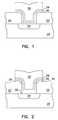
- FIG. 1is a cross-sectional representation of an aluminum interconnect formed in accordance with the method of the invention.
- FIG. 2is a cross-sectional representation of an embodiment wherein a titanium silicide layer is formed between an active device region and the interconnect.
- FIG. 3is a cross-sectional representation of an embodiment wherein a damascene aluminum interconnect is formed using the method of the invention.
- FIG. 4is a cross-sectional representation of an embodiment wherein a damascene aluminum interconnect is formed over a titanium silicide layer using the method of the invention.
- FIG. 5is a cross-sectional representation of a multi-level interconnect structure.
- wafer and substrate used in the following descriptioninclude any semiconductor-based structure. Wafer and substrate are used interchangeably to refer to supporting semiconductor structures 20 during processing, as illustrated in FIGS. 1 to 4 .
- interconnect viaa small grain size, conformal aluminum film in a via or contact, referred to herein as an interconnect via, in an integrated circuit (IC).
- ICintegrated circuit
- the inventionis particularly useful for forming aluminum films in sub-0.25 micron interconnect vias (contact holes) and interconnect vias having high-aspect ratios (i.e., ratio of height to diameter of an interconnect via), such as those greater than approximately 5:1.
- source/drain active regions of metal-oxide-semiconductor (MOS) transistorshave a particularly high aspect ratio of approximately 8:1.
- Interconnect structures illustrated in FIGS. 1 to 4are formed according to the method of the invention.
- an interconnectis etched in an isolating material 22 , such as silicon oxide or borophosphosilicate glass (BPSG) to define a semiconductor structure having a bottom surface, a top surface, and sidewalls of an interconnect via.
- the bottom surface of the interconnect viais an active region 24 of an IC, such as a source/drain region in a transistor.
- the top surface and sidewalls of the interconnect viacomprise the isolating material 22 in which the interconnect via is etched.
- the semiconductor structureis then placed in a chemical vapor deposition (CVD) reaction chamber.
- a titanium-containing organometallic precursorsuch as tetrakisdimethylamido titanium (TDMAT) or trimethylethylenediamino titanium (TMEDT), or another titanium-containing precursor gas, such as titanium tetrachloride is reacted in the CVD chamber.
- TDMATtetrakisdimethylamido titanium
- TEDTtrimethylethylenediamino titanium
- the main criteria for selecting a titanium-containing precursor gasis to assure that the precursor gas is capable of reacting in a CVD chamber to form a titanium nitride (TiN) film.
- a first layer of TiN 26is formed on the semiconductor structure, extending into the interconnect via, by reacting the titanium-containing precursor with nitrogen gas.
- the titanium-containing precursoris flowed at approximately 10 to 100 sccm.
- Nitrogenis flowed at approximately 10 to 1,000 sccm.
- Pressure in the CVD chamberis maintained at approximately 0.1 to 760 Torr.
- Temperature in the CVD chamberis maintained at approximately below the respective decomposition temperature for the precursor, but at a temperature that permits the precursor to be sufficiently capable of being volatilized in the CVD chamber. This method is applicable to any suitable type of CVD chamber, including cold-wall and hot-wall chambers. Consequently, temperature is also adjusted according to the type of CVD chamber used. These pressures and temperatures do not, however, appear to be highly critical to the deposition of the TiN layer 26 .
- the resulting TiN film 26is amorphous, preventing unwanted diffusion between the active device region 24 and the subsequently formed aluminum 30 .
- the thickness of the first layer of TiN 26is proportionate to the dimensions of the interconnect via. For example, for a 0.25 micron interconnect via, the thickness is approximately 100 to 200 angstroms.
- a second layer of TiN 28is then formed on the first layer of TiN 26 by reacting a titanium-containing precursor as described above with at least one of the following gases: ammonia and nitrogen trifluoride.
- the titanium-containing precursoris flowed at approximately 10 to 100 sccm.
- Ammonia or nitrogen trifluorideis flowed at approximately 10 to 1,000 sccm.
- other gasessuch as inert carrier gases or nitrogen, can be used in the CVD chamber during reaction to form the second layer of TiN 28 .
- gasesare flowed at approximately 10 to 1,000 sccm.
- Pressure in the CVD chamberis maintained at approximately 0.1 to 760 Torr.
- Temperature in the CVD chamberis maintained at approximately below the respective decomposition temperature for the precursor, but at a temperature such that the precursor is sufficiently capable of being volatilized in the CVD chamber.
- This methodis applicable using any suitable type of CVD chamber, including cold-wall and hot-wall chambers. Thus, temperature is also adjusted according to the type of CVD chamber used. Again, as in the deposition of TiN layer 26 , pressures and temperatures do not appear to be highly critical to the deposition of the TiN layer 28 .
- the resulting TiN film 28has a polycrystalline orientation.
- the grain orientation of the second layer of TiN 28comprises a mixture 1:1 of ⁇ 111> and ⁇ 200> orientated grains. It is preferred that this layer of TiN have a polycrystalline orientation, so that the subsequently formed aluminum 30 will have a small grain size and conformal shape due to the abundance of grain nucleation sites at boundaries between adjacent grains in the second TiN layer 28 . Such a plurality of nucleation sites enables small grains to form in the subsequently formed aluminum 30 . When there are many nucleation sites present, grains will nucleate and impinge on each other, preventing any of the grains from easily growing too big.
- the thickness of the second layer of TiN 28is proportionate to the dimensions of the interconnect via. For example, for a 0.25 micron interconnect via, the thickness is approximately 100 to 200 angstroms.
- An aluminum-containing organometallic precursorsuch as trimethylaluminum (TMA), dimethylaluminum hydride (DMAH), triisobutylaluminum (TIBA), triethylaluminum (TEA), diethylaluminum hydride (DEAH), monomethylaluminum hydride (MMAH), dimethylethylaminealane (DMEAA), or dimethylethylamide (DMEHA) is reacted in the CVD chamber in the presence of a carrier gas, such as inert gases to form the aluminum interconnect 30 .
- a carrier gassuch as inert gases
- the thickness of the aluminum 30 within the interconnect viais approximately 2,000 to 3,000 angstroms.
- more aluminum 30is also deposited outside of the interconnect via.
- approximately 1,000 to 2,000 angstroms of aluminumis also deposited above the top surface of the interconnect via.
- excess TiN 26 , 28 and aluminum 30is removed to form an interconnect structure as well known to one skilled in the art and illustrated in FIG. 1 .
- the presence of multiple, small grains in the aluminum 30enable the aluminum 30 to conform more easily to surfaces having complex topographies, such as high-aspect ratio interconnect vias. Improved conformality in aluminum interconnect 30 prevents formation of voids within the interconnect.
- a refractory metal silicide layer 32is formed on the bottom surface of the interconnect via prior to formation of the first or second TiN layers 26 and 28 and the aluminum 30 , as illustrated in FIG. 2 .
- the presence of a refractory metal silicide layer 32 between the active region 24 and the TiN diffusion barrier layer 26decreases resistivity of the contact by providing a layer of material 32 having an intermediate grain structure between that of silicon in the active region 24 and titanium in the TiN layer 26 .
- a refractory metal 34such as titanium is deposited over the semiconductor structure, extending into the interconnect via to a thickness proportional to the dimensions of the interconnect via. For example, for a 0.25 micron interconnect via, the thickness is approximately 100 to 200 angstroms.
- the structureis then annealed to form the refractory metal silicide 32 , such as titanium silicide, on those surfaces containing silicon, that support the titanium layer 34 .
- the active region 24 over which an interconnect is formedcontains silicon. Therefore, titanium silicide 32 forms only on the bottom surface of a interconnect via overlying an active region 24 . The remaining titanium 34 remains unreacted on the semiconductor structure.
- the final interconnect structures illustrated in FIGS. 1 and 2are polished so that the top surface of the final interconnect is coplanar with the top surface of the interconnect via, as illustrated in FIGS. 3 and 4 .
- Any type of polishing techniqueis used to form the damascene structures illustrated in FIGS. 3 and 4 .
- chemical mechanical polishingis used to polish the structure, as well known to one skilled in the art.
- FIG. 4illustrates one embodiment of the invention, in which a refractory metal silicide layer 32 is also formed in the damascene interconnect.
- the resulting damascene structuresutilize the aluminum 30 within the interconnect via as both an interconnect metal and metal line structures, which connect adjacent devices in an IC.
- FIG. 5illustrates a second interconnect connection formed between the first metal layer 30 and a second metal layer 40 .
- These layerscan be aluminum which is connected as described above using an interconnect via extending through an intermediate layer(s) of oxide 42 .
- a layer of TiN 44is provided as described above for layer 28 .
- multiple levels of interconnectscan be formed using the described methods.
- the inventionwas described above with reference to forming low resistivity interconnects in an IC.
- the method utilized for forming the small grain size, conformal aluminum films 30is applicable to forming aluminum films anywhere as desired over a supporting semiconductor structure.
- Resulting aluminum films 30have a lower resistivity than other types of metal films currently used, such as tungsten, and have a conformal shape due to the small grain size in the aluminum 30 .
- Such films 30are able to be easily formed over complex topographies.
- voidsare prevented from forming within the interconnect via. Unwanted voids degrade device performance, often causing shorts in the circuit.
- the present inventionprovides a method and apparatus for fabricating an interconnect supported by a semiconductor structure.
- a first layer of titanium nitrideis formed on the semiconductor structure.
- a second layer of titanium nitrideis formed on the first layer of titanium nitride.
- an aluminum filmis formed on the second layer of titanium nitride.
- a titanium silicide layeris optionally formed on the semiconductor structure prior to the step of forming the first layer of titanium nitride.
- a first titanium nitride layeris formed on an active device region to act as a barrier layer, protecting the integrity of the contact.
- an amorphous titanium nitride layeris formed by reacting a titanium-containing precursor in the presence of nitrogen.
- a second titanium nitride layeris formed on the first titanium nitride layer.
- the second titanium layerhas a polycrystalline orientation (having a mixture of grains orientated in the ⁇ 111> and ⁇ 200> directions), which allows diffusion between the active device region and the interconnect metal.
- the second titanium nitride layeris formed by reacting a titanium-containing precursor in the presence of at least ammonia (NH 3 ) or nitrogen trifluoride (NF 3 ).
- the titanium-containing precursors for forming the first and second layers of TiNare selected from the group consisting of: titanium tetrachloride, tetrakisdimethylamide titanium, and trimethylethylenediamino titanium.
- CVD aluminumis formed on the second titanium nitride layer to complete the interconnect. To form the CVD aluminum, an aluminum-containing precursor is used.
- the aluminum-containing precursoris selected from the group consisting of: trimethylaluminum (TMA), dimethylaluminum hydride (DMAH), triisobutylaluminum (TIBA), triethylaluminum (TEA), diethylaluminum hydride (DEAH), monomethylaluminum hydride (MMAH), dimethylethylalane (DMEHA1), and dimethylethylamide (DMEHA2).
- TMAtrimethylaluminum
- DMAHdimethylaluminum hydride
- TIBAtriisobutylaluminum
- TEAtriethylaluminum
- DEAHdiethylaluminum hydride
- MMAHmonomethylaluminum hydride
- DMEHA1dimethylethylalane
- DMEHA2dimethylethylamide
- a titanium silicide layeris formed between the first titanium nitride layer and the underlying active device region to further improve the ohmic characteristics of the contact.
- Titanium silicidehas an intermediate crystallographic structure between that of silicon in the active device region and titanium nitride. Thus, electronic carriers are able to diffuse easily through the interconnect structure.
- the crystal structure and grain size of the underlayersare controlled to promote subsequent formation of a small grain size, conformal aluminum film in an interconnect.
- the aluminum film formed according to the method of the inventionhas a polycrystalline orientation, with grain sizes of less than approximately 0.25 microns.
- interconnectsare formed with aluminum instead of tungsten, providing a lower resistivity contact to adjacent active device regions.
- such aluminum filmsare more conformal due to their smaller grain sizes. Vias are thus able to be filled with such aluminum to provide an interconnect structure substantially free of unwanted voids.
Landscapes
- Engineering & Computer Science (AREA)
- Physics & Mathematics (AREA)
- Condensed Matter Physics & Semiconductors (AREA)
- General Physics & Mathematics (AREA)
- Manufacturing & Machinery (AREA)
- Computer Hardware Design (AREA)
- Microelectronics & Electronic Packaging (AREA)
- Power Engineering (AREA)
- Chemical & Material Sciences (AREA)
- Chemical Kinetics & Catalysis (AREA)
- General Chemical & Material Sciences (AREA)
- Internal Circuitry In Semiconductor Integrated Circuit Devices (AREA)
Abstract
Description
Claims (33)
Priority Applications (1)
| Application Number | Priority Date | Filing Date | Title |
|---|---|---|---|
| US11/380,622US7737024B2 (en) | 1998-09-03 | 2006-04-27 | Small grain size, conformal aluminum interconnects and method for their formation |
Applications Claiming Priority (4)
| Application Number | Priority Date | Filing Date | Title |
|---|---|---|---|
| US09/146,509US6187673B1 (en) | 1998-09-03 | 1998-09-03 | Small grain size, conformal aluminum interconnects and method for their formation |
| US09/782,498US6774487B2 (en) | 1998-09-03 | 2001-02-13 | Small grain size, conformal aluminum interconnects and method for their formation |
| US10/899,736US7276795B2 (en) | 1998-09-03 | 2004-07-27 | Small grain size, conformal aluminum interconnects and method for their formation |
| US11/380,622US7737024B2 (en) | 1998-09-03 | 2006-04-27 | Small grain size, conformal aluminum interconnects and method for their formation |
Related Parent Applications (1)
| Application Number | Title | Priority Date | Filing Date |
|---|---|---|---|
| US10/899,736DivisionUS7276795B2 (en) | 1998-09-03 | 2004-07-27 | Small grain size, conformal aluminum interconnects and method for their formation |
Publications (2)
| Publication Number | Publication Date |
|---|---|
| US20060194434A1 US20060194434A1 (en) | 2006-08-31 |
| US7737024B2true US7737024B2 (en) | 2010-06-15 |
Family
ID=22517705
Family Applications (7)
| Application Number | Title | Priority Date | Filing Date |
|---|---|---|---|
| US09/146,509Expired - LifetimeUS6187673B1 (en) | 1998-09-03 | 1998-09-03 | Small grain size, conformal aluminum interconnects and method for their formation |
| US09/782,441Expired - Fee RelatedUS6946393B2 (en) | 1998-09-03 | 2001-02-13 | Small grain size, conformal aluminum interconnects and method for their formation |
| US09/782,498Expired - LifetimeUS6774487B2 (en) | 1998-09-03 | 2001-02-13 | Small grain size, conformal aluminum interconnects and method for their formation |
| US10/899,736Expired - LifetimeUS7276795B2 (en) | 1998-09-03 | 2004-07-27 | Small grain size, conformal aluminum interconnects and method for their formation |
| US11/230,773Expired - Fee RelatedUS7217661B2 (en) | 1998-09-03 | 2005-09-20 | Small grain size, conformal aluminum interconnects and method for their formation |
| US11/380,622Expired - LifetimeUS7737024B2 (en) | 1998-09-03 | 2006-04-27 | Small grain size, conformal aluminum interconnects and method for their formation |
| US11/897,842Expired - Fee RelatedUS7560816B2 (en) | 1998-09-03 | 2007-08-31 | Small grain size, conformal aluminum interconnects and method for their formation |
Family Applications Before (5)
| Application Number | Title | Priority Date | Filing Date |
|---|---|---|---|
| US09/146,509Expired - LifetimeUS6187673B1 (en) | 1998-09-03 | 1998-09-03 | Small grain size, conformal aluminum interconnects and method for their formation |
| US09/782,441Expired - Fee RelatedUS6946393B2 (en) | 1998-09-03 | 2001-02-13 | Small grain size, conformal aluminum interconnects and method for their formation |
| US09/782,498Expired - LifetimeUS6774487B2 (en) | 1998-09-03 | 2001-02-13 | Small grain size, conformal aluminum interconnects and method for their formation |
| US10/899,736Expired - LifetimeUS7276795B2 (en) | 1998-09-03 | 2004-07-27 | Small grain size, conformal aluminum interconnects and method for their formation |
| US11/230,773Expired - Fee RelatedUS7217661B2 (en) | 1998-09-03 | 2005-09-20 | Small grain size, conformal aluminum interconnects and method for their formation |
Family Applications After (1)
| Application Number | Title | Priority Date | Filing Date |
|---|---|---|---|
| US11/897,842Expired - Fee RelatedUS7560816B2 (en) | 1998-09-03 | 2007-08-31 | Small grain size, conformal aluminum interconnects and method for their formation |
Country Status (1)
| Country | Link |
|---|---|
| US (7) | US6187673B1 (en) |
Families Citing this family (16)
| Publication number | Priority date | Publication date | Assignee | Title |
|---|---|---|---|---|
| US6081034A (en)* | 1992-06-12 | 2000-06-27 | Micron Technology, Inc. | Low-resistance contact to silicon having a titanium silicide interface and an amorphous titanium carbonitride barrier layer |
| US6187673B1 (en) | 1998-09-03 | 2001-02-13 | Micron Technology, Inc. | Small grain size, conformal aluminum interconnects and method for their formation |
| DE10196677B4 (en)* | 2001-07-30 | 2014-03-13 | Mitsubishi Denki K.K. | Electrode structure and method of manufacturing a thin-film structural body |
| US20030036242A1 (en)* | 2001-08-16 | 2003-02-20 | Haining Yang | Methods of forming metal-comprising materials and capacitor electrodes; and capacitor constructions |
| EP1306898A1 (en)* | 2001-10-29 | 2003-05-02 | Dialog Semiconductor GmbH | Sub-milliohm on-chip interconnection |
| JP2003257970A (en)* | 2002-02-27 | 2003-09-12 | Nec Electronics Corp | Semiconductor device and wiring structure of the same |
| KR100555514B1 (en)* | 2003-08-22 | 2006-03-03 | 삼성전자주식회사 | Semiconductor memory device having low resistance tungsten wiring and its manufacturing method |
| US20050130383A1 (en)* | 2003-12-10 | 2005-06-16 | International Business Machines Corporation | Silicide resistor in beol layer of semiconductor device and method |
| RU2250513C1 (en)* | 2003-12-25 | 2005-04-20 | Маянц Денис Борисович | Information chart |
| US7439179B2 (en)* | 2005-06-22 | 2008-10-21 | Intel Corporation | Healing detrimental bonds in deposited materials |
| KR100842914B1 (en)* | 2006-12-28 | 2008-07-02 | 주식회사 하이닉스반도체 | Metal wiring formation method of semiconductor device |
| JP5334199B2 (en) | 2008-01-22 | 2013-11-06 | ルネサスエレクトロニクス株式会社 | Semiconductor device having capacitive element |
| US9224773B2 (en) | 2011-11-30 | 2015-12-29 | Taiwan Semiconductor Manufacturing Company, Ltd. | Metal shielding layer in backside illumination image sensor chips and methods for forming the same |
| KR102127778B1 (en)* | 2013-10-15 | 2020-06-29 | 삼성전자주식회사 | Method of fabricating a semiconductor device and the device |
| US10796996B2 (en)* | 2017-03-10 | 2020-10-06 | Taiwan Semiconductor Manufacturing Co., Ltd. | Semiconductor device and method of forming the same |
| US11515256B2 (en)* | 2021-01-27 | 2022-11-29 | Taiwan Semiconductor Manufacturing Company, Ltd. | Semiconductor structure and manufacturing method thereof |
Citations (34)
| Publication number | Priority date | Publication date | Assignee | Title |
|---|---|---|---|---|
| US4756810A (en) | 1986-12-04 | 1988-07-12 | Machine Technology, Inc. | Deposition and planarizing methods and apparatus |
| US4999160A (en) | 1989-12-04 | 1991-03-12 | Micron Technology, Inc. | Aluminum alloy containing copper, silicon and titanium for VLSI devices |
| US5108951A (en) | 1990-11-05 | 1992-04-28 | Sgs-Thomson Microelectronics, Inc. | Method for forming a metal contact |
| US5148259A (en) | 1986-08-19 | 1992-09-15 | Fujitsu Limited | Semiconductor device having thin film wiring layer of aluminum containing carbon |
| US5192589A (en) | 1991-09-05 | 1993-03-09 | Micron Technology, Inc. | Low-pressure chemical vapor deposition process for depositing thin titanium nitride films having low and stable resistivity |
| US5246881A (en) | 1993-04-14 | 1993-09-21 | Micron Semiconductor, Inc. | Low-pressure chemical vapor deposition process for depositing high-density, highly-conformal, titanium nitride films of low bulk resistivity |
| US5288665A (en) | 1992-08-12 | 1994-02-22 | Applied Materials, Inc. | Process for forming low resistance aluminum plug in via electrically connected to overlying patterned metal layer for integrated circuit structures |
| US5316972A (en) | 1989-09-26 | 1994-05-31 | Canon Kabushiki Kaisha | Process for forming deposited film by use of alkyl aluminum hydride and process for preparing semiconductor device |
| US5328873A (en) | 1989-09-09 | 1994-07-12 | Canon Kubushiki Kaisha | Process for forming deposited film by use of alkyl aluminum hydride |
| US5383970A (en) | 1991-12-26 | 1995-01-24 | Canon Kabushiki Kaisha | Chemical vapor deposition method for forming a deposited film with the use of a liquid raw material and apparatus suitable for practicing said method |
| US5384284A (en) | 1993-10-01 | 1995-01-24 | Micron Semiconductor, Inc. | Method to form a low resistant bond pad interconnect |
| US5420072A (en) | 1994-02-04 | 1995-05-30 | Motorola, Inc. | Method for forming a conductive interconnect in an integrated circuit |
| US5464666A (en) | 1995-02-06 | 1995-11-07 | Air Products And Chemicals, Inc. | Process for chemical vapor codeposition of copper and aluminum alloys |
| US5480684A (en) | 1994-09-01 | 1996-01-02 | Micron Technology, Inc. | Method of reducing carbon incorporation into films produced by chemical vapor deposition involving organometallic precursor compounds |
| US5523626A (en) | 1993-09-08 | 1996-06-04 | Nec Corporation | Semiconductor device and fabrication process therefor |
| US5552181A (en) | 1992-12-21 | 1996-09-03 | Kawasaki Steel Corporation | Method for supplying liquid material and process for forming thin films using the liquid material supplying method |
| US5654235A (en) | 1994-08-18 | 1997-08-05 | Oki Electric Industry Co., Ltd. | Method of manufacturing contact structure using barrier metal |
| US5700718A (en) | 1996-02-05 | 1997-12-23 | Micron Technology, Inc. | Method for increased metal interconnect reliability in situ formation of titanium aluminide |
| US5726100A (en) | 1996-06-27 | 1998-03-10 | Micron Technology, Inc. | Method of forming contact vias and interconnect channels in a dielectric layer stack with a single mask |
| US5834846A (en) | 1995-01-10 | 1998-11-10 | Kawasaki Steel Corporation | Semiconductor device with contact structure and method of manufacturing the same |
| US5843843A (en) | 1992-09-07 | 1998-12-01 | Samsung Electronics Co., Ltd. | Method for forming a wiring layer a semiconductor device |
| US5844318A (en) | 1997-02-18 | 1998-12-01 | Micron Technology, Inc. | Aluminum film for semiconductive devices |
| US5847463A (en) | 1997-08-22 | 1998-12-08 | Micron Technology, Inc. | Local interconnect comprising titanium nitride barrier layer |
| US5861344A (en) | 1996-01-31 | 1999-01-19 | Micron Technology, Inc. | Facet etch for improved step coverage of integrated circuit contacts |
| US5866205A (en) | 1996-02-09 | 1999-02-02 | Micron Technology, Inc. | Process for titanium nitride deposition using five- and six-coordinate titanium complexes |
| US5874131A (en) | 1996-10-02 | 1999-02-23 | Micron Technology, Inc. | CVD method for forming metal-containing films |
| US5939787A (en) | 1992-12-10 | 1999-08-17 | Samsung Electronics Co., Ltd. | Semiconductor device having a multi-layer contact structure |
| US5972179A (en) | 1997-09-30 | 1999-10-26 | Lucent Technologies Inc. | Silicon IC contacts using composite TiN barrier layer |
| US6077781A (en)* | 1995-11-21 | 2000-06-20 | Applied Materials, Inc. | Single step process for blanket-selective CVD aluminum deposition |
| US6077571A (en) | 1995-12-19 | 2000-06-20 | The Research Foundation Of State University Of New York | Conformal pure and doped aluminum coatings and a methodology and apparatus for their preparation |
| US6217721B1 (en) | 1995-08-07 | 2001-04-17 | Applied Materials, Inc. | Filling narrow apertures and forming interconnects with a metal utilizing a crystallographically oriented liner layer |
| US6271137B1 (en) | 1989-11-30 | 2001-08-07 | Stmicroelectronics, Inc. | Method of producing an aluminum stacked contact/via for multilayer |
| US6420260B1 (en) | 1997-03-27 | 2002-07-16 | Applied Materials, Inc. | Ti/Tinx underlayer which enables a highly <111> oriented aluminum interconnect |
| US6774487B2 (en) | 1998-09-03 | 2004-08-10 | Micron Technology, Inc. | Small grain size, conformal aluminum interconnects and method for their formation |
Family Cites Families (2)
| Publication number | Priority date | Publication date | Assignee | Title |
|---|---|---|---|---|
| US5325873A (en)* | 1992-07-23 | 1994-07-05 | Abbott Laboratories | Tube placement verifier system |
| DE60140657D1 (en)* | 2000-01-17 | 2010-01-14 | Eurand Pharmaceuticals Ltd | OCCUPANCY DISH, EXTRACTOR BATH, BATH ACCESSORY, DETERGENT TABLET, ORAL TABLET |
- 1998
- 1998-09-03USUS09/146,509patent/US6187673B1/ennot_activeExpired - Lifetime
- 2001
- 2001-02-13USUS09/782,441patent/US6946393B2/ennot_activeExpired - Fee Related
- 2001-02-13USUS09/782,498patent/US6774487B2/ennot_activeExpired - Lifetime
- 2004
- 2004-07-27USUS10/899,736patent/US7276795B2/ennot_activeExpired - Lifetime
- 2005
- 2005-09-20USUS11/230,773patent/US7217661B2/ennot_activeExpired - Fee Related
- 2006
- 2006-04-27USUS11/380,622patent/US7737024B2/ennot_activeExpired - Lifetime
- 2007
- 2007-08-31USUS11/897,842patent/US7560816B2/ennot_activeExpired - Fee Related
Patent Citations (41)
| Publication number | Priority date | Publication date | Assignee | Title |
|---|---|---|---|---|
| US5148259A (en) | 1986-08-19 | 1992-09-15 | Fujitsu Limited | Semiconductor device having thin film wiring layer of aluminum containing carbon |
| US4756810A (en) | 1986-12-04 | 1988-07-12 | Machine Technology, Inc. | Deposition and planarizing methods and apparatus |
| US5328873A (en) | 1989-09-09 | 1994-07-12 | Canon Kubushiki Kaisha | Process for forming deposited film by use of alkyl aluminum hydride |
| US5316972A (en) | 1989-09-26 | 1994-05-31 | Canon Kabushiki Kaisha | Process for forming deposited film by use of alkyl aluminum hydride and process for preparing semiconductor device |
| US6271137B1 (en) | 1989-11-30 | 2001-08-07 | Stmicroelectronics, Inc. | Method of producing an aluminum stacked contact/via for multilayer |
| US4999160A (en) | 1989-12-04 | 1991-03-12 | Micron Technology, Inc. | Aluminum alloy containing copper, silicon and titanium for VLSI devices |
| US5108951A (en) | 1990-11-05 | 1992-04-28 | Sgs-Thomson Microelectronics, Inc. | Method for forming a metal contact |
| US5192589A (en) | 1991-09-05 | 1993-03-09 | Micron Technology, Inc. | Low-pressure chemical vapor deposition process for depositing thin titanium nitride films having low and stable resistivity |
| US5383970A (en) | 1991-12-26 | 1995-01-24 | Canon Kabushiki Kaisha | Chemical vapor deposition method for forming a deposited film with the use of a liquid raw material and apparatus suitable for practicing said method |
| US5288665A (en) | 1992-08-12 | 1994-02-22 | Applied Materials, Inc. | Process for forming low resistance aluminum plug in via electrically connected to overlying patterned metal layer for integrated circuit structures |
| US5843843A (en) | 1992-09-07 | 1998-12-01 | Samsung Electronics Co., Ltd. | Method for forming a wiring layer a semiconductor device |
| US5939787A (en) | 1992-12-10 | 1999-08-17 | Samsung Electronics Co., Ltd. | Semiconductor device having a multi-layer contact structure |
| US5552181A (en) | 1992-12-21 | 1996-09-03 | Kawasaki Steel Corporation | Method for supplying liquid material and process for forming thin films using the liquid material supplying method |
| US5246881A (en) | 1993-04-14 | 1993-09-21 | Micron Semiconductor, Inc. | Low-pressure chemical vapor deposition process for depositing high-density, highly-conformal, titanium nitride films of low bulk resistivity |
| US5523626A (en) | 1993-09-08 | 1996-06-04 | Nec Corporation | Semiconductor device and fabrication process therefor |
| US5384284A (en) | 1993-10-01 | 1995-01-24 | Micron Semiconductor, Inc. | Method to form a low resistant bond pad interconnect |
| US5420072A (en) | 1994-02-04 | 1995-05-30 | Motorola, Inc. | Method for forming a conductive interconnect in an integrated circuit |
| US5654235A (en) | 1994-08-18 | 1997-08-05 | Oki Electric Industry Co., Ltd. | Method of manufacturing contact structure using barrier metal |
| US5480684A (en) | 1994-09-01 | 1996-01-02 | Micron Technology, Inc. | Method of reducing carbon incorporation into films produced by chemical vapor deposition involving organometallic precursor compounds |
| US5834846A (en) | 1995-01-10 | 1998-11-10 | Kawasaki Steel Corporation | Semiconductor device with contact structure and method of manufacturing the same |
| US5464666A (en) | 1995-02-06 | 1995-11-07 | Air Products And Chemicals, Inc. | Process for chemical vapor codeposition of copper and aluminum alloys |
| US6217721B1 (en) | 1995-08-07 | 2001-04-17 | Applied Materials, Inc. | Filling narrow apertures and forming interconnects with a metal utilizing a crystallographically oriented liner layer |
| US6077781A (en)* | 1995-11-21 | 2000-06-20 | Applied Materials, Inc. | Single step process for blanket-selective CVD aluminum deposition |
| US6077571A (en) | 1995-12-19 | 2000-06-20 | The Research Foundation Of State University Of New York | Conformal pure and doped aluminum coatings and a methodology and apparatus for their preparation |
| US5861344A (en) | 1996-01-31 | 1999-01-19 | Micron Technology, Inc. | Facet etch for improved step coverage of integrated circuit contacts |
| US5700718A (en) | 1996-02-05 | 1997-12-23 | Micron Technology, Inc. | Method for increased metal interconnect reliability in situ formation of titanium aluminide |
| US5866205A (en) | 1996-02-09 | 1999-02-02 | Micron Technology, Inc. | Process for titanium nitride deposition using five- and six-coordinate titanium complexes |
| US5726100A (en) | 1996-06-27 | 1998-03-10 | Micron Technology, Inc. | Method of forming contact vias and interconnect channels in a dielectric layer stack with a single mask |
| US5874131A (en) | 1996-10-02 | 1999-02-23 | Micron Technology, Inc. | CVD method for forming metal-containing films |
| US5844318A (en) | 1997-02-18 | 1998-12-01 | Micron Technology, Inc. | Aluminum film for semiconductive devices |
| US6420260B1 (en) | 1997-03-27 | 2002-07-16 | Applied Materials, Inc. | Ti/Tinx underlayer which enables a highly <111> oriented aluminum interconnect |
| US5847463A (en) | 1997-08-22 | 1998-12-08 | Micron Technology, Inc. | Local interconnect comprising titanium nitride barrier layer |
| US5972179A (en) | 1997-09-30 | 1999-10-26 | Lucent Technologies Inc. | Silicon IC contacts using composite TiN barrier layer |
| US6774487B2 (en) | 1998-09-03 | 2004-08-10 | Micron Technology, Inc. | Small grain size, conformal aluminum interconnects and method for their formation |
| US20050006774A1 (en) | 1998-09-03 | 2005-01-13 | Micron Technology, Inc. | Small grain size, conformal aluminum interconnects and method for their formation |
| US6946393B2 (en) | 1998-09-03 | 2005-09-20 | Micron Technology, Inc. | Small grain size, conformal aluminum interconnects and method for their formation |
| US20060014386A1 (en) | 1998-09-03 | 2006-01-19 | Micron Technology, Inc. | Small grain size, conformal aluminum interconnects and method for their formation |
| US7217661B2 (en) | 1998-09-03 | 2007-05-15 | Micron Technology, Inc. | Small grain size, conformal aluminum interconnects and method for their formation |
| US7276795B2 (en) | 1998-09-03 | 2007-10-02 | Micron Technology, Inc. | Small grain size, conformal aluminum interconnects and method for their formation |
| US20070296084A1 (en) | 1998-09-03 | 2007-12-27 | Micron Technology, Inc. | Small grain size, conformal aluminum interconnects and method for their formation |
| US7560816B2 (en) | 1998-09-03 | 2009-07-14 | Micron Technology, Inc. | Small grain size, conformal aluminum interconnects and method for their formation |
Non-Patent Citations (3)
| Title |
|---|
| Fiordalice, R. W., et al., "Orientation Control of Chemical Vapor Deposition TiN Film for Barrier Applications", Journal of the Electrochemical Society, 143(6), (Jun. 1996),pp. 2059-2063. |
| Lee, H., et al., "Study of Diffusion Barrier Performance in MOCVD TiN by Transmission Electron Microscopy", Materials Research Society Symposium Proceedings, 391, (1995),pp. 205-209. |
| Pramanik, D., et al., "Effect of Underlayer on Sputtered Aluminum Grain Structure and its Correlation with Step Coverage in Submicron Vias", 1990 Proceedings Seventh International IEEE VLSI Multilevel Interconnection Conference, IEEE Catalog No. 90TH0325-1,(Jun. 1990),pp. 332-334. |
Also Published As
| Publication number | Publication date |
|---|---|
| US20070296084A1 (en) | 2007-12-27 |
| US7560816B2 (en) | 2009-07-14 |
| US20060014386A1 (en) | 2006-01-19 |
| US7276795B2 (en) | 2007-10-02 |
| US20060194434A1 (en) | 2006-08-31 |
| US20010005621A1 (en) | 2001-06-28 |
| US20050006774A1 (en) | 2005-01-13 |
| US6187673B1 (en) | 2001-02-13 |
| US20010009807A1 (en) | 2001-07-26 |
| US6946393B2 (en) | 2005-09-20 |
| US7217661B2 (en) | 2007-05-15 |
| US6774487B2 (en) | 2004-08-10 |
Similar Documents
| Publication | Publication Date | Title |
|---|---|---|
| US7737024B2 (en) | Small grain size, conformal aluminum interconnects and method for their formation | |
| US6955983B2 (en) | Methods of forming metal interconnections of semiconductor devices by treating a barrier metal layer | |
| US6903462B2 (en) | Chemical vapor deposition of titanium | |
| US6376355B1 (en) | Method for forming metal interconnection in semiconductor device | |
| US6153519A (en) | Method of forming a barrier layer | |
| US7154178B2 (en) | Multilayer diffusion barrier for copper interconnections | |
| US6399490B1 (en) | Highly conformal titanium nitride deposition process for high aspect ratio structures | |
| US20060246714A1 (en) | Method of forming a conductive contact | |
| JPH08250497A (en) | Method for forming metal wiring layer of semiconductor device | |
| US6433434B1 (en) | Apparatus having a titanium alloy layer | |
| US7138337B2 (en) | Methods of forming tungsten contacts by chemical vapor deposition | |
| EP0840363A1 (en) | Method for fabricating a conductive diffusion barrier layer by PECVD | |
| KR100609049B1 (en) | Metal wiring formation method of semiconductor device | |
| EP0800206A2 (en) | Method of simultaneously forming a contact/via plug and an interconnect |
Legal Events
| Date | Code | Title | Description |
|---|---|---|---|
| FEPP | Fee payment procedure | Free format text:PAYOR NUMBER ASSIGNED (ORIGINAL EVENT CODE: ASPN); ENTITY STATUS OF PATENT OWNER: LARGE ENTITY | |
| STCF | Information on status: patent grant | Free format text:PATENTED CASE | |
| CC | Certificate of correction | ||
| FPAY | Fee payment | Year of fee payment:4 | |
| AS | Assignment | Owner name:U.S. BANK NATIONAL ASSOCIATION, AS COLLATERAL AGENT, CALIFORNIA Free format text:SECURITY INTEREST;ASSIGNOR:MICRON TECHNOLOGY, INC.;REEL/FRAME:038669/0001 Effective date:20160426 Owner name:U.S. BANK NATIONAL ASSOCIATION, AS COLLATERAL AGEN Free format text:SECURITY INTEREST;ASSIGNOR:MICRON TECHNOLOGY, INC.;REEL/FRAME:038669/0001 Effective date:20160426 | |
| AS | Assignment | Owner name:MORGAN STANLEY SENIOR FUNDING, INC., AS COLLATERAL AGENT, MARYLAND Free format text:PATENT SECURITY AGREEMENT;ASSIGNOR:MICRON TECHNOLOGY, INC.;REEL/FRAME:038954/0001 Effective date:20160426 Owner name:MORGAN STANLEY SENIOR FUNDING, INC., AS COLLATERAL Free format text:PATENT SECURITY AGREEMENT;ASSIGNOR:MICRON TECHNOLOGY, INC.;REEL/FRAME:038954/0001 Effective date:20160426 | |
| AS | Assignment | Owner name:U.S. BANK NATIONAL ASSOCIATION, AS COLLATERAL AGENT, CALIFORNIA Free format text:CORRECTIVE ASSIGNMENT TO CORRECT THE REPLACE ERRONEOUSLY FILED PATENT #7358718 WITH THE CORRECT PATENT #7358178 PREVIOUSLY RECORDED ON REEL 038669 FRAME 0001. ASSIGNOR(S) HEREBY CONFIRMS THE SECURITY INTEREST;ASSIGNOR:MICRON TECHNOLOGY, INC.;REEL/FRAME:043079/0001 Effective date:20160426 Owner name:U.S. BANK NATIONAL ASSOCIATION, AS COLLATERAL AGEN Free format text:CORRECTIVE ASSIGNMENT TO CORRECT THE REPLACE ERRONEOUSLY FILED PATENT #7358718 WITH THE CORRECT PATENT #7358178 PREVIOUSLY RECORDED ON REEL 038669 FRAME 0001. ASSIGNOR(S) HEREBY CONFIRMS THE SECURITY INTEREST;ASSIGNOR:MICRON TECHNOLOGY, INC.;REEL/FRAME:043079/0001 Effective date:20160426 | |
| MAFP | Maintenance fee payment | Free format text:PAYMENT OF MAINTENANCE FEE, 8TH YEAR, LARGE ENTITY (ORIGINAL EVENT CODE: M1552) Year of fee payment:8 | |
| AS | Assignment | Owner name:JPMORGAN CHASE BANK, N.A., AS COLLATERAL AGENT, ILLINOIS Free format text:SECURITY INTEREST;ASSIGNORS:MICRON TECHNOLOGY, INC.;MICRON SEMICONDUCTOR PRODUCTS, INC.;REEL/FRAME:047540/0001 Effective date:20180703 Owner name:JPMORGAN CHASE BANK, N.A., AS COLLATERAL AGENT, IL Free format text:SECURITY INTEREST;ASSIGNORS:MICRON TECHNOLOGY, INC.;MICRON SEMICONDUCTOR PRODUCTS, INC.;REEL/FRAME:047540/0001 Effective date:20180703 | |
| AS | Assignment | Owner name:MICRON TECHNOLOGY, INC., IDAHO Free format text:RELEASE BY SECURED PARTY;ASSIGNOR:U.S. BANK NATIONAL ASSOCIATION, AS COLLATERAL AGENT;REEL/FRAME:047243/0001 Effective date:20180629 | |
| AS | Assignment | Owner name:MICRON TECHNOLOGY, INC., IDAHO Free format text:RELEASE BY SECURED PARTY;ASSIGNOR:MORGAN STANLEY SENIOR FUNDING, INC., AS COLLATERAL AGENT;REEL/FRAME:050937/0001 Effective date:20190731 | |
| AS | Assignment | Owner name:MICRON SEMICONDUCTOR PRODUCTS, INC., IDAHO Free format text:RELEASE BY SECURED PARTY;ASSIGNOR:JPMORGAN CHASE BANK, N.A., AS COLLATERAL AGENT;REEL/FRAME:051028/0001 Effective date:20190731 Owner name:MICRON TECHNOLOGY, INC., IDAHO Free format text:RELEASE BY SECURED PARTY;ASSIGNOR:JPMORGAN CHASE BANK, N.A., AS COLLATERAL AGENT;REEL/FRAME:051028/0001 Effective date:20190731 |