US7736959B2 - Integrated circuit device, and method of fabricating same - Google Patents
Integrated circuit device, and method of fabricating sameDownload PDFInfo
- Publication number
- US7736959B2 US7736959B2US12/069,704US6970408AUS7736959B2US 7736959 B2US7736959 B2US 7736959B2US 6970408 AUS6970408 AUS 6970408AUS 7736959 B2US7736959 B2US 7736959B2
- Authority
- US
- United States
- Prior art keywords
- transistors
- memory
- section
- semiconductor
- logic
- Prior art date
- Legal status (The legal status is an assumption and is not a legal conclusion. Google has not performed a legal analysis and makes no representation as to the accuracy of the status listed.)
- Expired - Lifetime, expires
Links
Images


Classifications
- H—ELECTRICITY
- H10—SEMICONDUCTOR DEVICES; ELECTRIC SOLID-STATE DEVICES NOT OTHERWISE PROVIDED FOR
- H10B—ELECTRONIC MEMORY DEVICES
- H10B12/00—Dynamic random access memory [DRAM] devices
- H10B12/01—Manufacture or treatment
- H10B12/09—Manufacture or treatment with simultaneous manufacture of the peripheral circuit region and memory cells
- H—ELECTRICITY
- H10—SEMICONDUCTOR DEVICES; ELECTRIC SOLID-STATE DEVICES NOT OTHERWISE PROVIDED FOR
- H10B—ELECTRONIC MEMORY DEVICES
- H10B12/00—Dynamic random access memory [DRAM] devices
- H—ELECTRICITY
- H10—SEMICONDUCTOR DEVICES; ELECTRIC SOLID-STATE DEVICES NOT OTHERWISE PROVIDED FOR
- H10B—ELECTRONIC MEMORY DEVICES
- H10B12/00—Dynamic random access memory [DRAM] devices
- H10B12/01—Manufacture or treatment
- H—ELECTRICITY
- H10—SEMICONDUCTOR DEVICES; ELECTRIC SOLID-STATE DEVICES NOT OTHERWISE PROVIDED FOR
- H10B—ELECTRONIC MEMORY DEVICES
- H10B12/00—Dynamic random access memory [DRAM] devices
- H10B12/20—DRAM devices comprising floating-body transistors, e.g. floating-body cells
- H—ELECTRICITY
- H10—SEMICONDUCTOR DEVICES; ELECTRIC SOLID-STATE DEVICES NOT OTHERWISE PROVIDED FOR
- H10B—ELECTRONIC MEMORY DEVICES
- H10B12/00—Dynamic random access memory [DRAM] devices
- H10B12/30—DRAM devices comprising one-transistor - one-capacitor [1T-1C] memory cells
- H10B12/34—DRAM devices comprising one-transistor - one-capacitor [1T-1C] memory cells the transistor being at least partially in a trench in the substrate
- H—ELECTRICITY
- H10—SEMICONDUCTOR DEVICES; ELECTRIC SOLID-STATE DEVICES NOT OTHERWISE PROVIDED FOR
- H10B—ELECTRONIC MEMORY DEVICES
- H10B12/00—Dynamic random access memory [DRAM] devices
- H10B12/30—DRAM devices comprising one-transistor - one-capacitor [1T-1C] memory cells
- H10B12/36—DRAM devices comprising one-transistor - one-capacitor [1T-1C] memory cells the transistor being a FinFET
- H—ELECTRICITY
- H10—SEMICONDUCTOR DEVICES; ELECTRIC SOLID-STATE DEVICES NOT OTHERWISE PROVIDED FOR
- H10B—ELECTRONIC MEMORY DEVICES
- H10B12/00—Dynamic random access memory [DRAM] devices
- H10B12/50—Peripheral circuit region structures
- H—ELECTRICITY
- H10—SEMICONDUCTOR DEVICES; ELECTRIC SOLID-STATE DEVICES NOT OTHERWISE PROVIDED FOR
- H10D—INORGANIC ELECTRIC SEMICONDUCTOR DEVICES
- H10D30/00—Field-effect transistors [FET]
- H10D30/60—Insulated-gate field-effect transistors [IGFET]
- H10D30/711—Insulated-gate field-effect transistors [IGFET] having floating bodies
- H—ELECTRICITY
- H10—SEMICONDUCTOR DEVICES; ELECTRIC SOLID-STATE DEVICES NOT OTHERWISE PROVIDED FOR
- H10D—INORGANIC ELECTRIC SEMICONDUCTOR DEVICES
- H10D86/00—Integrated devices formed in or on insulating or conducting substrates, e.g. formed in silicon-on-insulator [SOI] substrates or on stainless steel or glass substrates
- H10D86/01—Manufacture or treatment
- H10D86/011—Manufacture or treatment comprising FinFETs
- H—ELECTRICITY
- H10—SEMICONDUCTOR DEVICES; ELECTRIC SOLID-STATE DEVICES NOT OTHERWISE PROVIDED FOR
- H10D—INORGANIC ELECTRIC SEMICONDUCTOR DEVICES
- H10D86/00—Integrated devices formed in or on insulating or conducting substrates, e.g. formed in silicon-on-insulator [SOI] substrates or on stainless steel or glass substrates
- H10D86/201—Integrated devices formed in or on insulating or conducting substrates, e.g. formed in silicon-on-insulator [SOI] substrates or on stainless steel or glass substrates the substrates comprising an insulating layer on a semiconductor body, e.g. SOI
- H10D86/215—Integrated devices formed in or on insulating or conducting substrates, e.g. formed in silicon-on-insulator [SOI] substrates or on stainless steel or glass substrates the substrates comprising an insulating layer on a semiconductor body, e.g. SOI comprising FinFETs
- H—ELECTRICITY
- H10—SEMICONDUCTOR DEVICES; ELECTRIC SOLID-STATE DEVICES NOT OTHERWISE PROVIDED FOR
- H10D—INORGANIC ELECTRIC SEMICONDUCTOR DEVICES
- H10D30/00—Field-effect transistors [FET]
- H10D30/60—Insulated-gate field-effect transistors [IGFET]
- H10D30/62—Fin field-effect transistors [FinFET]
Definitions
- SOISilicon-on-Insulator
- PDpartially depleted
- FDfully depleted
- Fin-FETfin-shaped field effect transistor
- SOI deviceshave demonstrated improved performance (for example, speed), reduced leakage current characteristics and considerable enhancement in scaling.
- multiple gate SOI transistor 10typically involves first defining (using conventional lithographic and etching techniques) an upper or top layer of silicon of SOI wafer 12 (typically having a thickness of 10 to 200 nm) to define segments or pieces 14 that constitute the active regions of transistor 10 (i.e., source 16 , drain 18 , and body 20 ). Thereafter, dielectric material is deposited or formed (for example, via oxidation) on silicon segments 12 to form gate dielectric 22 .
- a gate materialfor example, a highly conductive silicon-based material is then deposited and patterned to form gate 24 of transistor 10 which, as illustrated in FIG. 1A , is disposed on, juxtaposed and/or “covers” a plurality of interfaces (in the illustrative embodiment, three) of silicon segments or pieces 14 of SOI transistor 10 .
- FIG. 1Bis taken through the gate region and along the longitudinal axis of the gate region of FIG. 1A (along lines B-B′) and, as such, the source and drain regions are not illustrated because they are in a direction perpendicular to that axis.
- the cross-sectional view of FIG. 1Cis taken through the source and drain regions and perpendicular to the longitudinal axis of the gate (along lines C-C′).
- An advantage of such structuresis performance (for example, speed) because, in operation, a channel forms in the body adjacent or beneath each of the gate-body interfaces.
- a channelforms in the body adjacent or beneath each of the gate-body interfaces.
- three channelsmay form: two channels may be vertical and one channel may be horizontal. As such, the overall current drive of SOI transistor 10 is higher thereby facilitating higher performance or speed.
- transistorsmay be determined by selecting the width of the silicon segments or pieces 14 .
- the width of the silicon segments or pieces 14may be selected or designed so that during operation the full body of transistor 10 is fully depleted or controlled completely by the voltage applied to gate 24 .
- microprocessorsmay be well suited for microprocessors, microcontrollers or the like (hereinafter collectively “microprocessors”).
- microprocessorscurrently less than half of the die of a microprocessor is occupied by or contains advanced logic transistors.
- Memory cellsand peripheral circuitry reside on the remaining area of the die.
- memory cell 26 proposed for SOI materialsmay be based on, among other things, a floating body effect of SOI transistors.
- memory cell 26may consist of a PD or a FD SOI transistor 28 having a channel (between source region 30 and drain region 32 ), which is disposed adjacent to body region 34 and separated therefrom by gate dielectric.
- the body region 34is electrically floating.
- a gate 36is employed (in conjunction with source region 30 and drain region 32 , among other things) to control the operation of memory cell 26 .
- Such memory cellsin addition to having low leakage current characteristics, facilitate implementing high-density memory cell arrays. While it may be advantageous to integrate SOI logic transistors and SOI memory cells on a single die to, among other things, reduce the overall dimensions of the die, fabricating an integrated device having SOI logic transistors and SOI memory cells may be challenging because each have unique and/or differing fabrication considerations. There is a need for a method of fabricating an integrated circuit device comprised of high performance SOI transistors (for example, Fin-FET and multiple gate structures) and SOI memory cells (for example, PD or FD SOI memory cells). Indeed, there is a need for a high performance integrated circuit device having SOI logic (including high performance and/or non-high performance transistors) and SOI memory that each include improved performance (for example, speed), reduced leakage current characteristics and/or considerable enhancement in scaling and density.
- SOI logicincluding high performance and/or non-high performance transistors
- SOI memorythat each include improved performance (for example, speed), reduced leakage current characteristics and/
- the present inventionis an integrated circuit device disposed in or on a semiconductor layer which resides on or above an insulating layer of a substrate, the semiconductor integrated circuit device comprises a memory section and a logic section.
- the memory sectionincludes a plurality of memory cells wherein each memory cell includes a transistor having a source region, a drain region and a body region disposed between the source region and the drain region, wherein the body region is electrically floating.
- a gateis spaced apart from, and capacitively coupled to the body region.
- Each memory cellincludes a first data state and a second data state.
- the first data stateis representative of a first charge in the body region wherein the first charge is substantially provided by accumulating majority carriers in the body region.
- the second data staterepresentative of a second charge in the body region wherein the second charge is substantially provided by removing majority carriers from the body region.
- the logic sectionincluding a plurality of transistors wherein each transistor includes a source region, a drain region and a body region disposed between the source region and the drain region, wherein the source, drain and body regions are disposed in a segment of the semiconductor layer such that the body region includes a plurality of surfaces.
- a gateis spaced apart from and opposing the plurality of surfaces of the body region.
- the source, drain and body regions of a plurality of transistors of the logic sectionare contained in a segment of the semiconductor layer.
- the plurality of source, drain and body regions of the plurality of transistors of the logic sectionmay be contained in a plurality of segments of the semiconductor layer. Indeed, each segment of the plurality of segments contains source, drain and body regions of a plurality of transistors of the logic section.
- the source, drain and body regions of the transistors of the memory cellsare disposed in a segment of the semiconductor layer.
- the body region of each transistor of each memory cellincludes a plurality of surfaces and wherein the associated gate is spaced apart from and opposing the plurality of surfaces of the body region.
- the width of the gate of each transistor of the plurality of transistors of the logic sectionis less than the width of the gate of each transistor of each memory cell of the memory section.
- the present inventionis a method of manufacturing an integrated circuit device on an SOI wafer having a semiconductor layer disposed on an insulating layer.
- the integrated circuit deviceincludes (1) a logic section, including a plurality of transistors, and (2) a memory section, including a plurality of memory cells wherein each memory cell consists essentially of one transistor.
- the method of this aspect of the inventioncomprises forming a plurality of semiconductor pieces in the semiconductor layer of the SOI wafer associated with the logic section, wherein each piece includes a plurality of surfaces.
- the methodalso includes forming a memory section in the semiconductor layer of the SOI wafer.
- the memory sectionincludes a major surface.
- a dielectric materialmay be deposited on (i) the plurality of surfaces of the semiconductor pieces and (ii) the major surface of the memory section.
- a conductive materialmay be deposited above the dielectric material and a plurality of gates and associated gate dielectrics may be formed from the conductive material and dielectric material.
- the methodfurther includes providing source and drain regions in (i) the semiconductor pieces and (ii) the major surface of the memory section.
- the source and drain regions of the transistors in the memory sectionare formed in the major surface of the memory section via ion implantation.
- the source and drain regions of the transistors in the logic sectionmay also be formed in the semiconductor pieces via ion implantation.
- the present inventionis a method of manufacturing an integrated circuit device on an SOI wafer having a semiconductor layer disposed on an insulating layer.
- the integrated circuit deviceincludes (1) a logic section, including a plurality of transistors, and (2) a memory section, including a plurality of memory cells wherein each memory cell consists essentially of one transistor.
- the method of this aspect of the present inventionincludes forming a plurality of semiconductor pieces in the semiconductor layer of the SOI wafer associated with the logic section and the memory section, wherein each semiconductor piece includes a plurality of surfaces.
- the methodfurther includes depositing a dielectric material on the plurality of surfaces of the semiconductor pieces of the SOI wafer associated with the memory and logic sections.
- a conductive materialmay be deposited above the dielectric material, and a plurality of gates and associated gate dielectrics may be formed from the conductive material and the dielectric material.
- the source and drain regionsmay be formed in the semiconductor pieces of the SOI wafer associated with the memory and logic sections.
- the source and drain regions of the transistors in the memory sectionare formed in the semiconductor pieces of the SOI wafer associated with the memory section via ion implantation.
- the source and drain regions of the transistors in the logic sectionmay also be formed in the semiconductor pieces of the SOI wafer associated with the logic section via ion implantation.
- the width of the gates of each transistor of the plurality of transistors of the logic sectionis less than the width of the gate of each transistor of each memory cell of the memory section.
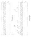
- FIG. 1Aillustrates a three dimensional view of Fin-FET or multiple gate SOI transistor
- FIGS. 1B and 1Cillustrate cross-sectional views of a semiconductor transistor as illustrated in FIG. 1A , sectioned along lines B-B′ and C-C′, respectively;
- FIG. 2Aillustrates a three dimensional view of one embodiment of a semiconductor transistor as illustrated (and described) in the Semiconductor Memory Device Patent Application;
- FIGS. 2B and 2Cillustrate cross-sectional views of a semiconductor transistor as illustrated in FIG. 2A , sectioned along lines B-B′ and C-C′, respectively;
- FIG. 3Ais a schematic representation of a portion of a DRAM array as illustrated (and described) in one embodiment of the Semiconductor Memory Device Patent Application;
- FIG. 3Billustrates a memory cell according to one embodiment of the Semiconductor Memory Device Patent Application
- FIGS. 4A and 4Bare exemplary schematic illustrations of the charge relationship, for a particular memory state, of the floating body, source and drain regions of a memory cell according to one embodiment of the Semiconductor Memory Device Patent Application;
- FIGS. 5A and 5Billustrate an integrated circuit device including a memory section having, for example, PD or FD SOI memory cells, and a logic section having, for example, high performance transistors, such as Fin-FET, multiple gate transistors, and/or non-high performance transistors, according to certain embodiments of certain aspects of the present inventions;
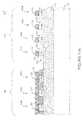
- FIGS. 6-10 and 11 Aillustrate cross-sectional views of the fabrication of the integrated circuit of FIG. 5A at various stages of an exemplary process, according to certain aspects of the present invention
- FIG. 11Billustrates cross-sectional view of the fabrication of the integrated circuit of FIG. 5B at a stage of an exemplary process, according to certain aspects of the present invention
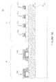
- FIG. 12illustrates an integrated circuit device including a memory section having, for example, PD or FD SOI memory cells, and a logic section having, for example, high performance transistors, such as Fin-FET, multiple gate transistors, and/or non-high performance transistors, according to certain embodiments of another aspect of the present invention
- FIGS. 13-16illustrate cross-sectional views of the fabrication of the integrated circuit of FIG. 12 at various stages of an exemplary process, according to certain aspects of the present invention.
- FIGS. 17A-17Cillustrate an integrated circuit device including a memory section having, for example, PD or FD SOI memory cells, and a logic section having, for example, high and/or non-high performance transistors, according to other embodiments of the present invention.
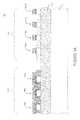
- integrated circuit device 100includes memory section 102 having, for example, PD or FD SOI memory cells 104 a - d , and logic section 106 having, for example, high performance transistors 108 a - c , such as Fin-FET, multiple gate transistors, and/or non-high performance transistors (for example, single gate transistors that do not possess the performance characteristics of high performance transistors—not illustrated).
- memory section 102having, for example, PD or FD SOI memory cells 104 a - d
- logic section 106having, for example, high performance transistors 108 a - c , such as Fin-FET, multiple gate transistors, and/or non-high performance transistors (for example, single gate transistors that do not possess the performance characteristics of high performance transistors—not illustrated).
- an exemplary method of fabricating or manufacturing an integrated circuit 100may begin with SOI wafer 110 including substrate 112 (comprised of, for example, a semiconductor material (for example, silicon) or a glass-like or insulator-like material) and insulator 114 (comprised of, for example, silicon oxide or silicon nitride, or combinations thereof) disposed thereon.
- the SOI waferincludes semiconductor layer 116 (comprised of, for example, silicon or germanium, or combinations thereof) disposed on insulator 114 .
- memory and logic sections 102 and 106 , respectively, of integrated circuit device 100may be formed in or on semiconductor layer 116 .
- semiconductor layer 116may be patterned (using conventional lithographic and etching techniques) to generally define memory section 102 and logic section 106 .
- semiconductor layer 116is patterned to provide semiconductor segments 118 a that will be employed as the active areas of the transistors (for example, the source, drain and body of the transistors) of logic section 106 (see, FIG. 7 ).
- semiconductor section 118 bremains generally unpatterned.
- dielectric layer 120for example, silicon oxide, silicon nitride or combinations thereof, such as an oxide-nitride-oxide material
- the deposition, formation and/or growth of the dielectric materialis selective.
- a layer of dielectricis deposited, formed and/or grown in a non-selective manner and that layer is later patterned using conventional lithographic and etching techniques.
- highly conductive layer 122(comprised of, for example, heavily doped silicon, germanium, gallium arsenide, metal or metal compound) may then be deposited on dielectric layer 120 (see, FIG. 9 ).
- the highly conductive layer 122may then be patterned to form gates 124 of transistors 108 a - c and memory cells 104 a - d (see, FIG. 10 ) and transistors 108 a - b and/or memory cells 104 a - d (see, for example, FIGS. 11A and 11B ).
- dielectric material 120 disposed on semiconductor segment 118 bmay be patterned before and/or after deposition, formation and/or patterning of highly conductive layer 122 .
- the source regions 126 and drain regions 128 of memory cells 104 and transistors 108may be formed using conventional techniques (for example, via ion implantation) using the associated gate as a mask (see, FIGS. 11A and 11B ).
- source and drain implantsmay be performed before deposition and formation of gates 124 . Indeed, the source and/or drain regions 126 and 128 (respectively) may be performed at other (earlier and/or later) steps in the fabrication process flow.
- gates 124 of the transistors of memory cells 104 and gates 124 of transistors 108may be interconnected in various ways in order to provide a predetermined circuit configuration, function or operation.
- selected or predetermined gates 124 of transistors 108may be connected to provide a particular circuit, function or operation. (See, FIG. 11A ).
- the fabrication process of integrated circuit device 100may continue with the backend processing, including, for example, transistor interconnection, contact formation, passivating material deposition, and packaging (if any).
- integrated circuit device 100includes memory section 102 including memory cells 104 having transistor dimensions that provide, maximize and/or enhance the “memory effect”.
- logic section 106may include high performance transistors 108 having dimensions that minimize, reduce and/or eliminate “memory effect” to increase the speed and/or predictability of the transistors in logic section 106 .
- memory cells 104may include transistor dimensions that provide, maximize and/or increase the “memory effect” to, for example, provide suitable and/or enhance the data retention characteristics of the transistors of memory cells 104 .
- changes in the “memory effect”may be implemented using greater different impurity doping levels of silicon segments or pieces in or near the body region of (i) the transistor of memory cells 104 and (ii) transistors 108 of logic section 106 .
- the impurity doping levels of the silicon segments or pieces in or near the body region of the transistor of memory cells 104may be greater than the impurity doping levels of the silicon segments or pieces in or near the body region of transistors 108 of logic section 106 .
- the entire contents of the Semiconductor Device Patent Application IIincluding, for example, the inventions, features, attributes, architectures, configurations, materials, techniques and advantages described and illustrated therein, are hereby incorporated by reference herein.
- an additional buried impurity regionmay be incorporated within memory section 102 and/or memory cells 104 as, for example, described and illustrated in the Semiconductor Device Patent Application II. Again, those discussions are incorporated by reference herein in their entirety.
- differing characteristicsmay be obtained by employing different widths of the silicon segment of memory cells 104 and transistors 108 .
- the transistors of memory cells 104i.e., the FinFET or multi gate transistors in memory section 102
- the transistors of memory cells 104may behave more like typical PD or FD transistors.
- FIG. 12See, for example, FIG. 12 .
- all techniques to increase, enhance and/or maximize the “memory effect” of the transistors of memory section 102 (relative to transistors 108 of logic section 106 ), whether now known or later developed,are intended to come within the scope of the present invention.
- An exemplary method of fabricating or manufacturing an integrated circuit according to the embodiment illustrated in FIG. 12may begin with an SOI wafer. (See, for example, FIG. 6 ). Thereafter, semiconductor layer 116 may be patterned (using conventional lithographic and etching techniques), to provide memory section 102 , including semiconductor segments or pieces 118 b , that will be employed as the active areas (for example, the source, drain and body of the transistors) of the transistors of memory cells 104 (see, FIG. 13 ).
- the logic section 106includes semiconductor segments 118 a having width that is less than the channel width of the transistors of memory cells 104 (for example, less than the width of semiconductor segments 118 b which are patterned and etched in memory section 102 of integrated circuit device 100 ).
- a dielectric layer(comprised of, for example, silicon oxide, silicon nitride or combinations thereof, such as an oxide-nitride-oxide) may then be deposited, formed and/or grown on semiconductor segments 118 (see, FIG. 14 ).
- a highly conductive materialfor example, a layer of heavily doped silicon, germanium, gallium arsenide, metal or metal compound, or combinations thereof
- the highly conductive materialmay be patterned to provide gates 124 of the transistors of memory cells 104 as well as gates 124 of transistors 108 (see, for example, FIG. 12 ).
- the source regions and drain regionsare formed via ion implantation using the gate of the transistors as a mask (see, for example, FIG. 16 ).
- source and drain regionsare performed before deposition and formation of the gates of the transistors. Indeed, the source/drain regions may be performed at other steps in the process.
- gates 124 of the transistors of memory cells 104 and gates 124 of transistors 108 of logic section 106may be interconnected in various ways in order to provide a predetermined circuit configuration, function or operation. (See, FIGS. 17A-17C ).
- selected or predetermined gates 124 of transistors 108may be connected to provide a particular circuit, function or operation. (See, FIG. 17C ).
- SOI wafer 12may include a top or device layer of, for example, silicon (as described above), germanium, silicon/germanium, and gallium arsenide or any other semiconductor material, whether now known or later developed, in which transistors may be formed. All such materials are intended to fall within the scope of the present invention.
- SOI wafer 12may be prepared and/or fabricated using a number of conventional techniques.
- SOI wafer 12may be a SIMOX wafer fabricated using well-known techniques including those disclosed, mentioned or referenced in U.S. Pat. Nos. 5,053,627; 5,080,730; 5,196,355; 5,288,650; 6,248,642; 6,417,078; 6,423,975; and 6,433,342 and U.S. Published Patent Applications 2002/0081824 and 2002 / 0123211 , the contents of which are hereby incorporated by reference.
- all types, materials and/or fabrication techniques of or for SOI wafers, whether now known or later developed,are intended to fall within the scope of the present invention.
- the memory cell(s) 104may also employ the structure, features, attributes, architectures, configurations, materials, techniques and advantages described and illustrated in the following non-provisional U.S. patent applications:
- the memory cellsmay be arranged, configured and/or controlled using any of the memory cell arrays, architectures and/or control/operation techniques described and illustrated in the above-referenced four (4) non-provisional U.S. patent applications. For the sake of brevity, those discussions will not be repeated; such memory cell arrays, architectures and/or control/operation techniques are incorporated herein by reference.
- the sensor described and illustrated in the Semiconductor Memory Device Patent Applicationmay also be implemented in the present invention.
- that sensormay be integrated with logic and/or memory cells/transistors, of the type described above (for example, the high performance and non-high performance transistors).
- the fabrication techniques and flow described and illustrated hereinare exemplary embodiments. It is to be understood that other embodiments may be employed, including changes and additions of those described and illustrated, without departing from the scope of the present invention.
- the transistors of the logic and/or memory sectionsmay include “halo” implants and threshold adjust implants to, for example, enhance or optimize the performance of the transistors.
Landscapes
- Engineering & Computer Science (AREA)
- Manufacturing & Machinery (AREA)
- Thin Film Transistor (AREA)
- Semiconductor Memories (AREA)
- Metal-Oxide And Bipolar Metal-Oxide Semiconductor Integrated Circuits (AREA)
Abstract
Description
Claims (17)
Priority Applications (1)
| Application Number | Priority Date | Filing Date | Title |
|---|---|---|---|
| US12/069,704US7736959B2 (en) | 2003-07-22 | 2008-02-12 | Integrated circuit device, and method of fabricating same |
Applications Claiming Priority (3)
| Application Number | Priority Date | Filing Date | Title |
|---|---|---|---|
| US48926603P | 2003-07-22 | 2003-07-22 | |
| US10/884,481US7335934B2 (en) | 2003-07-22 | 2004-07-02 | Integrated circuit device, and method of fabricating same |
| US12/069,704US7736959B2 (en) | 2003-07-22 | 2008-02-12 | Integrated circuit device, and method of fabricating same |
Related Parent Applications (1)
| Application Number | Title | Priority Date | Filing Date |
|---|---|---|---|
| US10/884,481DivisionUS7335934B2 (en) | 2003-07-22 | 2004-07-02 | Integrated circuit device, and method of fabricating same |
Publications (2)
| Publication Number | Publication Date |
|---|---|
| US20080153213A1 US20080153213A1 (en) | 2008-06-26 |
| US7736959B2true US7736959B2 (en) | 2010-06-15 |
Family
ID=34083508
Family Applications (2)
| Application Number | Title | Priority Date | Filing Date |
|---|---|---|---|
| US10/884,481Expired - LifetimeUS7335934B2 (en) | 2003-07-22 | 2004-07-02 | Integrated circuit device, and method of fabricating same |
| US12/069,704Expired - LifetimeUS7736959B2 (en) | 2003-07-22 | 2008-02-12 | Integrated circuit device, and method of fabricating same |
Family Applications Before (1)
| Application Number | Title | Priority Date | Filing Date |
|---|---|---|---|
| US10/884,481Expired - LifetimeUS7335934B2 (en) | 2003-07-22 | 2004-07-02 | Integrated circuit device, and method of fabricating same |
Country Status (2)
| Country | Link |
|---|---|
| US (2) | US7335934B2 (en) |
| WO (1) | WO2005008778A1 (en) |
Cited By (1)
| Publication number | Priority date | Publication date | Assignee | Title |
|---|---|---|---|---|
| US11251189B2 (en) | 2009-02-09 | 2022-02-15 | Longitude Flash Memory Solutions Ltd. | Gate fringing effect based channel formation for semiconductor device |
Families Citing this family (78)
| Publication number | Priority date | Publication date | Assignee | Title |
|---|---|---|---|---|
| US7335934B2 (en)* | 2003-07-22 | 2008-02-26 | Innovative Silicon S.A. | Integrated circuit device, and method of fabricating same |
| US20050062088A1 (en)* | 2003-09-22 | 2005-03-24 | Texas Instruments Incorporated | Multi-gate one-transistor dynamic random access memory |
| US20050077574A1 (en)* | 2003-10-08 | 2005-04-14 | Chandra Mouli | 1T/0C RAM cell with a wrapped-around gate device structure |
| US7253650B2 (en)* | 2004-05-25 | 2007-08-07 | International Business Machines Corporation | Increase productivity at wafer test using probe retest data analysis |
| US7547945B2 (en)* | 2004-09-01 | 2009-06-16 | Micron Technology, Inc. | Transistor devices, transistor structures and semiconductor constructions |
| JP4064955B2 (en)* | 2004-09-30 | 2008-03-19 | 株式会社東芝 | Semiconductor device and manufacturing method thereof |
| US7301803B2 (en)* | 2004-12-22 | 2007-11-27 | Innovative Silicon S.A. | Bipolar reading technique for a memory cell having an electrically floating body transistor |
| DE602005006093T2 (en)* | 2005-02-21 | 2009-05-20 | Interuniversitair Microelektronica Centrum (Imec) | Semiconductor memory device with floating body and manufacturing method thereof |
| DE102005007822B4 (en)* | 2005-02-21 | 2014-05-22 | Infineon Technologies Ag | Integrated circuit arrangement with tunnel field effect transistor |
| US7384849B2 (en) | 2005-03-25 | 2008-06-10 | Micron Technology, Inc. | Methods of forming recessed access devices associated with semiconductor constructions |
| US7282401B2 (en) | 2005-07-08 | 2007-10-16 | Micron Technology, Inc. | Method and apparatus for a self-aligned recessed access device (RAD) transistor gate |
| US7352018B2 (en)* | 2005-07-22 | 2008-04-01 | Infineon Technologies Ag | Non-volatile memory cells and methods for fabricating non-volatile memory cells |
| US20070023833A1 (en)* | 2005-07-28 | 2007-02-01 | Serguei Okhonin | Method for reading a memory cell having an electrically floating body transistor, and memory cell and array implementing same |
| KR101168976B1 (en)* | 2005-08-18 | 2012-07-26 | 삼성전자주식회사 | Semiconductor memory device |
| US7867851B2 (en) | 2005-08-30 | 2011-01-11 | Micron Technology, Inc. | Methods of forming field effect transistors on substrates |
| US7606066B2 (en)* | 2005-09-07 | 2009-10-20 | Innovative Silicon Isi Sa | Memory cell and memory cell array having an electrically floating body transistor, and methods of operating same |
| US7355916B2 (en)* | 2005-09-19 | 2008-04-08 | Innovative Silicon S.A. | Method and circuitry to generate a reference current for reading a memory cell, and device implementing same |
| US20070085140A1 (en)* | 2005-10-19 | 2007-04-19 | Cedric Bassin | One transistor memory cell having strained electrically floating body region, and method of operating same |
| US7326976B2 (en)* | 2005-11-15 | 2008-02-05 | International Business Machines Corporation | Corner dominated trigate field effect transistor |
| US7301210B2 (en)* | 2006-01-12 | 2007-11-27 | International Business Machines Corporation | Method and structure to process thick and thin fins and variable fin to fin spacing |
| US7700441B2 (en)* | 2006-02-02 | 2010-04-20 | Micron Technology, Inc. | Methods of forming field effect transistors, methods of forming field effect transistor gates, methods of forming integrated circuitry comprising a transistor gate array and circuitry peripheral to the gate array, and methods of forming integrated circuitry comprising a transistor gate array including first gates and second grounded isolation gates |
| US7542345B2 (en)* | 2006-02-16 | 2009-06-02 | Innovative Silicon Isi Sa | Multi-bit memory cell having electrically floating body transistor, and method of programming and reading same |
| US7473946B2 (en)* | 2006-02-22 | 2009-01-06 | International Business Machines Corporation | CMOS structure and method including multiple crystallographic planes |
| US7977736B2 (en)* | 2006-02-23 | 2011-07-12 | Samsung Electronics Co., Ltd. | Vertical channel transistors and memory devices including vertical channel transistors |
| US7492632B2 (en) | 2006-04-07 | 2009-02-17 | Innovative Silicon Isi Sa | Memory array having a programmable word length, and method of operating same |
| US7606098B2 (en) | 2006-04-18 | 2009-10-20 | Innovative Silicon Isi Sa | Semiconductor memory array architecture with grouped memory cells, and method of controlling same |
| US7933142B2 (en)* | 2006-05-02 | 2011-04-26 | Micron Technology, Inc. | Semiconductor memory cell and array using punch-through to program and read same |
| US8069377B2 (en)* | 2006-06-26 | 2011-11-29 | Micron Technology, Inc. | Integrated circuit having memory array including ECC and column redundancy and method of operating the same |
| US8946811B2 (en) | 2006-07-10 | 2015-02-03 | Taiwan Semiconductor Manufacturing Company, Ltd. | Body-tied, strained-channel multi-gate device and methods of manufacturing same |
| US7542340B2 (en)* | 2006-07-11 | 2009-06-02 | Innovative Silicon Isi Sa | Integrated circuit including memory array having a segmented bit line architecture and method of controlling and/or operating same |
| US7602001B2 (en) | 2006-07-17 | 2009-10-13 | Micron Technology, Inc. | Capacitorless one transistor DRAM cell, integrated circuitry comprising an array of capacitorless one transistor DRAM cells, and method of forming lines of capacitorless one transistor DRAM cells |
| US7772632B2 (en)* | 2006-08-21 | 2010-08-10 | Micron Technology, Inc. | Memory arrays and methods of fabricating memory arrays |
| US7589995B2 (en)* | 2006-09-07 | 2009-09-15 | Micron Technology, Inc. | One-transistor memory cell with bias gate |
| US7410856B2 (en)* | 2006-09-14 | 2008-08-12 | Micron Technology, Inc. | Methods of forming vertical transistors |
| US7592209B2 (en)* | 2006-11-13 | 2009-09-22 | Intel Corporation | Integration of a floating body memory on SOI with logic transistors on bulk substrate |
| US8217435B2 (en)* | 2006-12-22 | 2012-07-10 | Intel Corporation | Floating body memory cell having gates favoring different conductivity type regions |
| KR101277402B1 (en) | 2007-01-26 | 2013-06-20 | 마이크론 테크놀로지, 인코포레이티드 | Floating-body dram transistor comprising source/drain regions separated from the gated body region |
| US8518774B2 (en)* | 2007-03-29 | 2013-08-27 | Micron Technology, Inc. | Manufacturing process for zero-capacitor random access memory circuits |
| US8064274B2 (en)* | 2007-05-30 | 2011-11-22 | Micron Technology, Inc. | Integrated circuit having voltage generation circuitry for memory cell array, and method of operating and/or controlling same |
| US8085594B2 (en) | 2007-06-01 | 2011-12-27 | Micron Technology, Inc. | Reading technique for memory cell with electrically floating body transistor |
| US7923373B2 (en) | 2007-06-04 | 2011-04-12 | Micron Technology, Inc. | Pitch multiplication using self-assembling materials |
| KR101357304B1 (en)* | 2007-09-11 | 2014-01-28 | 삼성전자주식회사 | Capacitorless DRAM and methods of manufacturing and operating the same |
| WO2009039169A1 (en) | 2007-09-17 | 2009-03-26 | Innovative Silicon S.A. | Refreshing data of memory cells with electrically floating body transistors |
| US20090078999A1 (en)* | 2007-09-20 | 2009-03-26 | Anderson Brent A | Semiconductor device structures with floating body charge storage and methods for forming such semiconductor device structures. |
| US8536628B2 (en) | 2007-11-29 | 2013-09-17 | Micron Technology, Inc. | Integrated circuit having memory cell array including barriers, and method of manufacturing same |
| US8349662B2 (en)* | 2007-12-11 | 2013-01-08 | Micron Technology, Inc. | Integrated circuit having memory cell array, and method of manufacturing same |
| US8773933B2 (en) | 2012-03-16 | 2014-07-08 | Micron Technology, Inc. | Techniques for accessing memory cells |
| US8014195B2 (en) | 2008-02-06 | 2011-09-06 | Micron Technology, Inc. | Single transistor memory cell |
| US8189376B2 (en)* | 2008-02-08 | 2012-05-29 | Micron Technology, Inc. | Integrated circuit having memory cells including gate material having high work function, and method of manufacturing same |
| US7957206B2 (en) | 2008-04-04 | 2011-06-07 | Micron Technology, Inc. | Read circuitry for an integrated circuit having memory cells and/or a memory cell array, and method of operating same |
| US7947543B2 (en)* | 2008-09-25 | 2011-05-24 | Micron Technology, Inc. | Recessed gate silicon-on-insulator floating body device with self-aligned lateral isolation |
| US7933140B2 (en) | 2008-10-02 | 2011-04-26 | Micron Technology, Inc. | Techniques for reducing a voltage swing |
| US7924630B2 (en)* | 2008-10-15 | 2011-04-12 | Micron Technology, Inc. | Techniques for simultaneously driving a plurality of source lines |
| US8223574B2 (en)* | 2008-11-05 | 2012-07-17 | Micron Technology, Inc. | Techniques for block refreshing a semiconductor memory device |
| US8213226B2 (en) | 2008-12-05 | 2012-07-03 | Micron Technology, Inc. | Vertical transistor memory cell and array |
| US8319294B2 (en)* | 2009-02-18 | 2012-11-27 | Micron Technology, Inc. | Techniques for providing a source line plane |
| WO2010102106A2 (en)* | 2009-03-04 | 2010-09-10 | Innovative Silicon Isi Sa | Techniques for forming a contact to a buried diffusion layer in a semiconductor memory device |
| US8748959B2 (en)* | 2009-03-31 | 2014-06-10 | Micron Technology, Inc. | Semiconductor memory device |
| US8139418B2 (en)* | 2009-04-27 | 2012-03-20 | Micron Technology, Inc. | Techniques for controlling a direct injection semiconductor memory device |
| US8508994B2 (en) | 2009-04-30 | 2013-08-13 | Micron Technology, Inc. | Semiconductor device with floating gate and electrically floating body |
| US8498157B2 (en) | 2009-05-22 | 2013-07-30 | Micron Technology, Inc. | Techniques for providing a direct injection semiconductor memory device |
| US8537610B2 (en)* | 2009-07-10 | 2013-09-17 | Micron Technology, Inc. | Techniques for providing a semiconductor memory device |
| US9076543B2 (en) | 2009-07-27 | 2015-07-07 | Micron Technology, Inc. | Techniques for providing a direct injection semiconductor memory device |
| US8199595B2 (en)* | 2009-09-04 | 2012-06-12 | Micron Technology, Inc. | Techniques for sensing a semiconductor memory device |
| US8174881B2 (en) | 2009-11-24 | 2012-05-08 | Micron Technology, Inc. | Techniques for reducing disturbance in a semiconductor device |
| EP2329715B1 (en) | 2009-12-01 | 2013-02-20 | Cognis IP Management GmbH | Biocide compositions comprising branched alkyl polyglycosides |
| US8455334B2 (en)* | 2009-12-04 | 2013-06-04 | International Business Machines Corporation | Planar and nanowire field effect transistors |
| US8310893B2 (en)* | 2009-12-16 | 2012-11-13 | Micron Technology, Inc. | Techniques for reducing impact of array disturbs in a semiconductor memory device |
| US8416636B2 (en)* | 2010-02-12 | 2013-04-09 | Micron Technology, Inc. | Techniques for controlling a semiconductor memory device |
| US8411513B2 (en)* | 2010-03-04 | 2013-04-02 | Micron Technology, Inc. | Techniques for providing a semiconductor memory device having hierarchical bit lines |
| US8576631B2 (en)* | 2010-03-04 | 2013-11-05 | Micron Technology, Inc. | Techniques for sensing a semiconductor memory device |
| US8369177B2 (en)* | 2010-03-05 | 2013-02-05 | Micron Technology, Inc. | Techniques for reading from and/or writing to a semiconductor memory device |
| US8547738B2 (en) | 2010-03-15 | 2013-10-01 | Micron Technology, Inc. | Techniques for providing a semiconductor memory device |
| US8411524B2 (en) | 2010-05-06 | 2013-04-02 | Micron Technology, Inc. | Techniques for refreshing a semiconductor memory device |
| US8531878B2 (en) | 2011-05-17 | 2013-09-10 | Micron Technology, Inc. | Techniques for providing a semiconductor memory device |
| US9559216B2 (en) | 2011-06-06 | 2017-01-31 | Micron Technology, Inc. | Semiconductor memory device and method for biasing same |
| US10804394B2 (en)* | 2018-09-20 | 2020-10-13 | Avago Technologies International Sales Pte. Limited | Fin structures on a fully depleted semiconductor layer including a channel region |
| JP2025106682A (en)* | 2024-01-04 | 2025-07-16 | Rapidus株式会社 | Semiconductor device and method for manufacturing the same |
Citations (184)
| Publication number | Priority date | Publication date | Assignee | Title |
|---|---|---|---|---|
| US3439214A (en) | 1968-03-04 | 1969-04-15 | Fairchild Camera Instr Co | Beam-junction scan converter |
| FR2197494A5 (en) | 1972-08-25 | 1974-03-22 | Radiotechnique Compelec | |
| GB1414228A (en) | 1972-04-25 | 1975-11-19 | Ibm | Semiconductor storage devices |
| US3997799A (en) | 1975-09-15 | 1976-12-14 | Baker Roger T | Semiconductor-device for the storage of binary data |
| US4032947A (en) | 1971-10-20 | 1977-06-28 | Siemens Aktiengesellschaft | Controllable charge-coupled semiconductor device |
| US4250569A (en) | 1978-11-15 | 1981-02-10 | Fujitsu Limited | Semiconductor memory device |
| US4262340A (en) | 1978-11-14 | 1981-04-14 | Fujitsu Limited | Semiconductor memory device |
| US4298962A (en) | 1979-01-25 | 1981-11-03 | Nippon Electric Co., Ltd. | Memory |
| US4371955A (en) | 1979-02-22 | 1983-02-01 | Fujitsu Limited | Charge-pumping MOS FET memory device |
| EP0030856B1 (en) | 1979-12-13 | 1984-03-21 | Fujitsu Limited | Charge-pumping semiconductor memory cell comprising a charge-storage region and memory device using such a cell |
| US4527181A (en) | 1980-08-28 | 1985-07-02 | Fujitsu Limited | High density semiconductor memory array and method of making same |
| US4630089A (en) | 1983-09-27 | 1986-12-16 | Fujitsu Limited | Semiconductor memory device |
| US4791610A (en) | 1985-05-24 | 1988-12-13 | Fujitsu Limited | Semiconductor memory device formed of a SOI-type transistor and a capacitor |
| EP0207819B1 (en) | 1985-05-30 | 1989-08-23 | ETAT-FRANCAIS représenté par le DELEGUE GENERAL POUR L'ARMEMENT (DPAG) | Non-piezoelectric resonator with a high q factor |
| EP0354348A2 (en) | 1988-08-10 | 1990-02-14 | International Business Machines Corporation | CMOS-transistor and one-capacitor dram cell and fabrication process therefor |
| US4979014A (en) | 1987-08-10 | 1990-12-18 | Kabushiki Kaisha Toshiba | MOS transistor |
| EP0202515B1 (en) | 1982-11-04 | 1991-03-13 | Hitachi, Ltd. | Semiconductor memory |
| EP0175378B1 (en) | 1984-09-21 | 1991-11-21 | Fujitsu Limited | Dynamic random access memory (dram) |
| EP0253631B1 (en) | 1986-07-14 | 1992-04-22 | Oki Electric Industry Company, Limited | Semiconductor memory device |
| JPH04176163A (en) | 1990-11-08 | 1992-06-23 | Fujitsu Ltd | Semiconductor device and manufacture thereof |
| US5144390A (en) | 1988-09-02 | 1992-09-01 | Texas Instruments Incorporated | Silicon-on insulator transistor with internal body node to source node connection |
| EP0300157B1 (en) | 1987-07-20 | 1993-05-05 | International Business Machines Corporation | Vertical transistor capacitor memory cell structure and fabrication method therefor |
| EP0564204A2 (en) | 1992-03-30 | 1993-10-06 | Mitsubishi Denki Kabushiki Kaisha | Semiconductor device |
| US5258635A (en) | 1988-09-06 | 1993-11-02 | Kabushiki Kaisha Toshiba | MOS-type semiconductor integrated circuit device |
| EP0350057B1 (en) | 1988-07-07 | 1993-12-01 | Kabushiki Kaisha Toshiba | Semiconductor memory |
| EP0579566A2 (en) | 1992-06-17 | 1994-01-19 | International Business Machines Corporation | High-density dram structure on SOI |
| EP0362961B1 (en) | 1988-10-03 | 1994-02-16 | Interuniversitair Microelektronica Centrum Vzw | A method of operating a MOS-structure and MOS-structure therefor |
| EP0599506A1 (en) | 1992-11-27 | 1994-06-01 | International Business Machines Corporation | Semiconductor memory cell with SOI MOSFET |
| US5350938A (en) | 1990-06-27 | 1994-09-27 | Kabushiki Kaisha Toshiba | Nonvolatile semiconductor memory circuit with high speed read-out |
| US5355330A (en) | 1991-08-29 | 1994-10-11 | Hitachi, Ltd. | Capacitive memory having a PN junction writing and tunneling through an insulator of a charge holding electrode |
| EP0359551B1 (en) | 1988-09-14 | 1994-12-28 | Kawasaki Steel Corporation | Semicoductor memory circuit |
| US5388068A (en) | 1990-05-02 | 1995-02-07 | Microelectronics & Computer Technology Corp. | Superconductor-semiconductor hybrid memory circuits with superconducting three-terminal switching devices |
| EP0366882B1 (en) | 1988-10-31 | 1995-05-24 | International Business Machines Corporation | An ultra dense DRAM cell array and its method of fabrication |
| EP0465961B1 (en) | 1990-07-09 | 1995-08-09 | Sony Corporation | Semiconductor device on a dielectric isolated substrate |
| US5446299A (en) | 1994-04-29 | 1995-08-29 | International Business Machines Corporation | Semiconductor random access memory cell on silicon-on-insulator with dual control gates |
| US5448513A (en) | 1993-12-02 | 1995-09-05 | Regents Of The University Of California | Capacitorless DRAM device on silicon-on-insulator substrate |
| EP0513923B1 (en) | 1991-05-15 | 1995-09-27 | Koninklijke Philips Electronics N.V. | Protected programmable transistor with reduced parasitic capacitances and method of fabrication |
| US5489792A (en) | 1994-04-07 | 1996-02-06 | Regents Of The University Of California | Silicon-on-insulator transistors having improved current characteristics and reduced electrostatic discharge susceptibility |
| EP0333426B1 (en) | 1988-03-15 | 1996-07-10 | Kabushiki Kaisha Toshiba | Dynamic RAM |
| JPH08213624A (en) | 1995-02-08 | 1996-08-20 | Fujitsu Ltd | Semiconductor memory device and operating method thereof |
| EP0727820A1 (en) | 1995-02-17 | 1996-08-21 | Hitachi, Ltd. | Semiconductor memory device and method of manufacturing the same |
| US5568356A (en) | 1995-04-18 | 1996-10-22 | Hughes Aircraft Company | Stacked module assembly including electrically interconnected switching module and plural electronic modules |
| EP0739097A2 (en) | 1995-04-21 | 1996-10-23 | Nippon Telegraph And Telephone Corporation | MOSFET circuit and CMOS logic circuit using the same |
| EP0694977A3 (en) | 1994-07-14 | 1996-11-06 | Nec Corp | SOI-type semiconductor device with suppression of extension of the depletion region |
| JPH08316337A (en) | 1995-05-12 | 1996-11-29 | Nec Corp | Semiconductor memory device |
| US5593912A (en) | 1994-10-06 | 1997-01-14 | International Business Machines Corporation | SOI trench DRAM cell for 256 MB DRAM and beyond |
| US5606188A (en) | 1995-04-26 | 1997-02-25 | International Business Machines Corporation | Fabrication process and structure for a contacted-body silicon-on-insulator dynamic random access memory |
| EP0245515B1 (en) | 1985-11-20 | 1997-04-16 | Hitachi, Ltd. | Semiconductor device |
| US5627092A (en) | 1994-09-26 | 1997-05-06 | Siemens Aktiengesellschaft | Deep trench dram process on SOI for low leakage DRAM cell |
| US5631186A (en) | 1992-12-30 | 1997-05-20 | Samsung Electronics Co., Ltd. | Method for making a dynamic random access memory using silicon-on-insulator techniques |
| EP0788165A2 (en) | 1996-02-02 | 1997-08-06 | Siemens Aktiengesellschaft | Storage cell arrangement and method for making the same |
| US5696718A (en) | 1994-11-10 | 1997-12-09 | Commissariat A L'energie Atomique | Device having an electrically erasable non-volatile memory and process for producing such a device |
| EP0510607B1 (en) | 1991-04-23 | 1998-02-04 | Canon Kabushiki Kaisha | Semiconductor memory device |
| US5740099A (en) | 1995-02-07 | 1998-04-14 | Nec Corporation | Semiconductor memory device having peripheral circuit and interface circuit fabricated on bulk region out of silicon-on-insulator region for memory cells |
| US5778243A (en) | 1996-07-03 | 1998-07-07 | International Business Machines Corporation | Multi-threaded cell for a memory |
| US5780906A (en) | 1995-06-21 | 1998-07-14 | Micron Technology, Inc. | Static memory cell and method of manufacturing a static memory cell |
| US5784311A (en) | 1997-06-13 | 1998-07-21 | International Business Machines Corporation | Two-device memory cell on SOI for merged logic and memory applications |
| EP0858109A2 (en) | 1997-02-07 | 1998-08-12 | Nec Corporation | Semiconductor memory device and method for manufacturing thereof |
| EP0537677B1 (en) | 1991-10-16 | 1998-08-19 | Sony Corporation | Method of forming an SOI structure with a DRAM |
| EP0860878A2 (en) | 1997-02-20 | 1998-08-26 | Texas Instruments Incorporated | An integrated circuit with programmable elements |
| US5811283A (en) | 1996-08-13 | 1998-09-22 | United Microelectronics Corporation | Silicon on insulator (SOI) dram cell structure and process |
| EP0869511A2 (en) | 1997-04-02 | 1998-10-07 | Sony Corporation | Semiconductor memory cell and method of manufacturing the same |
| US5877978A (en) | 1996-03-04 | 1999-03-02 | Mitsubishi Denki Kabushiki Kaisha | Semiconductor memory device |
| US5886376A (en) | 1996-07-01 | 1999-03-23 | International Business Machines Corporation | EEPROM having coplanar on-insulator FET and control gate |
| US5886385A (en) | 1996-08-22 | 1999-03-23 | Kabushiki Kaisha Toshiba | Semiconductor device and manufacturing method thereof |
| US5897351A (en) | 1997-02-20 | 1999-04-27 | Micron Technology, Inc. | Method for forming merged transistor structure for gain memory cell |
| EP0801427A3 (en) | 1996-04-11 | 1999-05-06 | Matsushita Electric Industrial Co., Ltd. | Field effect transistor, semiconductor storage device, method of manufacturing the same and method of driving semiconductor storage device |
| EP0920059A2 (en) | 1997-11-28 | 1999-06-02 | Siemens Aktiengesellschaft | Memory cell array and method of producing the same |
| EP0924768A2 (en) | 1997-12-10 | 1999-06-23 | Matsushita Electronics Corporation | Nonvolatile semiconductor memory device and method for driving the same |
| EP0878804A3 (en) | 1997-05-15 | 1999-07-14 | STMicroelectronics, Inc. | Multiple transistor dynamic random access memory array architecture with simultaneous refresh of multiple memory cells during a read operation |
| EP0642173B1 (en) | 1993-08-19 | 1999-07-14 | Hitachi, Ltd. | Semiconductor element and semiconductor memory device using the same |
| US5929479A (en) | 1996-10-21 | 1999-07-27 | Nec Corporation | Floating gate type non-volatile semiconductor memory for storing multi-value information |
| US5930648A (en) | 1996-12-30 | 1999-07-27 | Hyundai Electronics Industries Co., Ltd. | Semiconductor memory device having different substrate thickness between memory cell area and peripheral area and manufacturing method thereof |
| US5936265A (en) | 1996-03-25 | 1999-08-10 | Kabushiki Kaisha Toshiba | Semiconductor device including a tunnel effect element |
| EP0727822B1 (en) | 1995-02-14 | 1999-08-11 | Canon Kabushiki Kaisha | Semiconductor memory device |
| US5943581A (en) | 1997-11-05 | 1999-08-24 | Vanguard International Semiconductor Corporation | Method of fabricating a buried reservoir capacitor structure for high-density dynamic random access memory (DRAM) circuits |
| US5943258A (en) | 1997-12-24 | 1999-08-24 | Texas Instruments Incorporated | Memory with storage cells having SOI drive and access transistors with tied floating body connections |
| EP0951072A1 (en) | 1996-04-08 | 1999-10-20 | Hitachi, Ltd. | Semiconductor integrated circuit device |
| US5977578A (en) | 1995-12-06 | 1999-11-02 | Micron Technology, Inc. | Method of forming dynamic random access memory circuitry and dynamic random access memory |
| EP0971360A1 (en) | 1992-12-10 | 2000-01-12 | Sony Corporation | Semiconductor memory cell |
| US6018172A (en) | 1994-09-26 | 2000-01-25 | Mitsubishi Denki Kabushiki Kaisha | Semiconductor memory device including memory cell transistors formed on SOI substrate and having fixed body regions |
| EP0980101A2 (en) | 1998-08-11 | 2000-02-16 | Hitachi, Ltd. | Semiconductor integrated circuit and method for manufacturing the same |
| EP0993037A2 (en) | 1998-09-29 | 2000-04-12 | Texas Instruments Incorporated | Method for two-sided fabrication of a memory array |
| US6097056A (en) | 1998-04-28 | 2000-08-01 | International Business Machines Corporation | Field effect transistor having a floating gate |
| US6096598A (en) | 1998-10-29 | 2000-08-01 | International Business Machines Corporation | Method for forming pillar memory cells and device formed thereby |
| EP0599388B1 (en) | 1992-11-20 | 2000-08-02 | Koninklijke Philips Electronics N.V. | Semiconductor device provided with a programmable element |
| EP0689252B1 (en) | 1990-03-20 | 2000-08-02 | Nec Corporation | Semiconductor device |
| US6111778A (en) | 1999-05-10 | 2000-08-29 | International Business Machines Corporation | Body contacted dynamic memory |
| EP0682370B1 (en) | 1994-05-13 | 2000-09-06 | Canon Kabushiki Kaisha | Storage device |
| JP2000247735A (en) | 1999-03-01 | 2000-09-12 | Murata Mfg Co Ltd | Production of low-temperature sintered ceramic composition |
| JP2000274221A (en) | 1999-03-18 | 2000-10-03 | Dr Ing H C F Porsche Ag | Lubricant container for internal combustion engine |
| US6157216A (en) | 1999-04-22 | 2000-12-05 | International Business Machines Corporation | Circuit driver on SOI for merged logic and memory circuits |
| US6171923B1 (en) | 1997-11-20 | 2001-01-09 | Vanguard International Semiconductor Corporation | Method for fabricating a DRAM cell structure on an SOI wafer incorporating a two dimensional trench capacitor |
| US6177708B1 (en) | 1998-08-07 | 2001-01-23 | International Business Machines Corporation | SOI FET body contact structure |
| EP1073121A2 (en) | 1999-07-29 | 2001-01-31 | Fujitsu Limited | Semiconductor memory device and method for manufacturing the same |
| US6214694B1 (en) | 1998-11-17 | 2001-04-10 | International Business Machines Corporation | Process of making densely patterned silicon-on-insulator (SOI) region on a wafer |
| US6225158B1 (en) | 1998-05-28 | 2001-05-01 | International Business Machines Corporation | Trench storage dynamic random access memory cell with vertical transfer device |
| JP3171768B2 (en) | 1995-04-13 | 2001-06-04 | 株式会社クボタ | Transmission braking system with HST |
| US6252281B1 (en) | 1995-03-27 | 2001-06-26 | Kabushiki Kaisha Toshiba | Semiconductor device having an SOI substrate |
| JP2001180633A (en) | 1999-12-27 | 2001-07-03 | Toshiba Tec Corp | Label printer |
| US6292424B1 (en) | 1995-01-20 | 2001-09-18 | Kabushiki Kaisha Toshiba | DRAM having a power supply voltage lowering circuit |
| US6297090B1 (en) | 1998-08-14 | 2001-10-02 | Samsung Electronics Co., Ltd. | Method for fabricating a high-density semiconductor memory device |
| US6320227B1 (en) | 1998-12-26 | 2001-11-20 | Hyundai Electronics Industries Co., Ltd. | Semiconductor memory device and method for fabricating the same |
| EP1162744A1 (en) | 2000-06-05 | 2001-12-12 | Mitsubishi Denki Kabushiki Kaisha | Semiconductor integrated circuit device operating with low power consumption |
| EP1162663A2 (en) | 2000-06-06 | 2001-12-12 | Infineon Technologies AG | DRAM memory cell and method of making the same |
| US6333532B1 (en) | 1999-07-16 | 2001-12-25 | International Business Machines Corporation | Patterned SOI regions in semiconductor chips |
| US6333222B1 (en)* | 1999-03-17 | 2001-12-25 | Mitsubishi Denki Kabushiki Kaisha | Semiconductor device and manufacturing method thereof |
| US20010055859A1 (en) | 2000-06-26 | 2001-12-27 | Kabushiki Kaisha Toshiba | Semiconductor device and method of fabricating the same |
| EP1179850A2 (en) | 2000-08-11 | 2002-02-13 | Fujio Masuoka | A semiconductor memory and its production process |
| US6350653B1 (en) | 2000-10-12 | 2002-02-26 | International Business Machines Corporation | Embedded DRAM on silicon-on-insulator substrate |
| US6351426B1 (en) | 1995-01-20 | 2002-02-26 | Kabushiki Kaisha Toshiba | DRAM having a power supply voltage lowering circuit |
| US20020030214A1 (en) | 2000-09-11 | 2002-03-14 | Fumio Horiguchi | Semiconductor device and method for manufacturing the same |
| US6359802B1 (en) | 2000-03-28 | 2002-03-19 | Intel Corporation | One-transistor and one-capacitor DRAM cell for logic process technology |
| US20020034855A1 (en) | 2000-09-08 | 2002-03-21 | Fumio Horiguchi | Semiconductor memory device and its manufacturing method |
| US20020036322A1 (en) | 2000-03-17 | 2002-03-28 | Ramachandra Divakauni | SOI stacked dram logic |
| US20020051378A1 (en) | 2000-08-17 | 2002-05-02 | Takashi Ohsawa | Semiconductor memory device and method of manufacturing the same |
| US6391658B1 (en) | 1999-10-26 | 2002-05-21 | International Business Machines Corporation | Formation of arrays of microelectronic elements |
| US6403435B1 (en) | 2000-07-21 | 2002-06-11 | Hyundai Electronics Industries Co., Ltd. | Method for fabricating a semiconductor device having recessed SOI structure |
| US20020072155A1 (en) | 2000-12-08 | 2002-06-13 | Chih-Cheng Liu | Method of fabricating a DRAM unit |
| US20020070411A1 (en) | 2000-09-08 | 2002-06-13 | Alcatel | Method of processing a high voltage p++/n-well junction and a device manufactured by the method |
| US20020076880A1 (en) | 2000-06-12 | 2002-06-20 | Takashi Yamada | Semiconductor device and method of fabricating the same |
| US20020086463A1 (en) | 2000-12-30 | 2002-07-04 | Houston Theodore W. | Means for forming SOI |
| US20020089038A1 (en) | 2000-10-20 | 2002-07-11 | International Business Machines Corporation | Fully-depleted-collector silicon-on-insulator (SOI) bipolar transistor useful alone or in SOI BiCMOS |
| US6424016B1 (en) | 1996-05-24 | 2002-07-23 | Texas Instruments Incorporated | SOI DRAM having P-doped polysilicon gate for a memory pass transistor |
| US6424011B1 (en) | 1997-04-14 | 2002-07-23 | International Business Machines Corporation | Mixed memory integration with NVRAM, dram and sram cell structures on same substrate |
| US20020098643A1 (en) | 1997-02-28 | 2002-07-25 | Kabushiki Kaisha Toshiba | Method of manufacturing SOI element having body contact |
| US6429477B1 (en) | 2000-10-31 | 2002-08-06 | International Business Machines Corporation | Shared body and diffusion contact structure and method for fabricating same |
| US6432768B1 (en)* | 2000-02-21 | 2002-08-13 | United Microelectronics Corp. | Method of fabricating memory device and logic device on the same chip |
| EP0744772B1 (en) | 1995-05-24 | 2002-08-14 | Infineon Technologies AG | DRAM storage cell with vertical transistor and method for production thereof |
| US20020110018A1 (en) | 2001-02-15 | 2002-08-15 | Takashi Ohsawa | Semiconductor memory device |
| EP1233454A2 (en) | 2001-02-19 | 2002-08-21 | Kabushiki Kaisha Toshiba | Semiconductor memory device and method of manufacturing the same |
| US6440872B1 (en) | 2000-11-03 | 2002-08-27 | International Business Machines Corporation | Method for hybrid DRAM cell utilizing confined strap isolation |
| US6441435B1 (en) | 2001-01-31 | 2002-08-27 | Advanced Micro Devices, Inc. | SOI device with wrap-around contact to underside of body, and method of making |
| US6441436B1 (en) | 2000-11-29 | 2002-08-27 | United Microelectronics Corp. | SOI device and method of fabrication |
| EP1241708A2 (en) | 2001-03-15 | 2002-09-18 | Kabushiki Kaisha Toshiba | Semiconductor memory device with floating body |
| EP0725402B1 (en) | 1995-01-05 | 2002-09-25 | Kabushiki Kaisha Toshiba | Semiconductor memory device |
| US6466511B2 (en) | 2000-06-30 | 2002-10-15 | Kabushiki Kaisha Toshiba | Semiconductor memory having double data rate transfer technique |
| EP1253634A2 (en) | 2001-04-26 | 2002-10-30 | Kabushiki Kaisha Toshiba | Semiconductor device |
| JP2002329795A (en) | 2001-04-26 | 2002-11-15 | Toshiba Corp | Semiconductor memory device and method of manufacturing the same |
| JP2002343886A (en) | 2001-03-15 | 2002-11-29 | Toshiba Corp | Semiconductor memory device |
| JP2002353080A (en) | 2001-03-21 | 2002-12-06 | Toshiba Corp | Semiconductor wafer, semiconductor device manufacturing apparatus, semiconductor device manufacturing method, and semiconductor wafer manufacturing method |
| US6492211B1 (en) | 2000-09-07 | 2002-12-10 | International Business Machines Corporation | Method for novel SOI DRAM BICMOS NPN |
| US20020195637A1 (en)* | 2001-06-26 | 2002-12-26 | Koichi Kokubun | Semiconductor device having trench capacitor formed in SOI substrate, and method of manufacturing the same |
| US20030015757A1 (en) | 2001-07-19 | 2003-01-23 | Takashi Ohsawa | Semiconductor memory device |
| US6518105B1 (en) | 2001-12-10 | 2003-02-11 | Taiwan Semiconductor Manufacturing Company | High performance PD SOI tunneling-biased MOSFET |
| US20030035324A1 (en) | 2001-08-17 | 2003-02-20 | Kabushiki Kaisha Toshiba | Semiconductor memory device |
| US6531754B1 (en) | 2001-12-28 | 2003-03-11 | Kabushiki Kaisha Toshiba | Manufacturing method of partial SOI wafer, semiconductor device using the partial SOI wafer and manufacturing method thereof |
| US20030057487A1 (en) | 2001-09-27 | 2003-03-27 | Kabushiki Kaisha Toshiba | Semiconductor chip having multiple functional blocks integrated in a single chip and method for fabricating the same |
| US20030057490A1 (en) | 2001-09-26 | 2003-03-27 | Kabushiki Kaisha Toshiba | Semiconductor device substrate and method of manufacturing semiconductor device substrate |
| US6549450B1 (en) | 2000-11-08 | 2003-04-15 | Ibm Corporation | Method and system for improving the performance on SOI memory arrays in an SRAM architecture system |
| US6552398B2 (en) | 2001-01-16 | 2003-04-22 | Ibm Corporation | T-Ram array having a planar cell structure and method for fabricating the same |
| US6556477B2 (en) | 2001-05-21 | 2003-04-29 | Ibm Corporation | Integrated chip having SRAM, DRAM and flash memory and method for fabricating the same |
| US20030085424A1 (en) | 2001-11-02 | 2003-05-08 | International Business Machines Corporation | Transistor structure with thick recessed source/drain structures and fabrication process of same |
| JP2003132682A (en) | 2001-08-17 | 2003-05-09 | Toshiba Corp | Semiconductor memory device |
| US6566177B1 (en) | 1999-10-25 | 2003-05-20 | International Business Machines Corporation | Silicon-on-insulator vertical array device trench capacitor DRAM |
| US20030102497A1 (en) | 2001-12-04 | 2003-06-05 | International Business Machines Corporation | Multiple-plane finFET CMOS |
| US20030102518A1 (en) | 2001-12-04 | 2003-06-05 | International Business Machines Corporation | Finfet SRAM cell using low mobility plane for cell stability and method for forming |
| US20030123279A1 (en) | 2002-01-03 | 2003-07-03 | International Business Machines Corporation | Silicon-on-insulator SRAM cells with increased stability and yield |
| US6597014B1 (en)* | 1997-08-19 | 2003-07-22 | Semiconductor Energy Laboratory Co., Ltd. | Semiconductor device and semiconductor display device |
| US6597034B2 (en) | 1997-08-29 | 2003-07-22 | Semiconductor Energy Laboratory Co., Ltd. | Non-volatile memory and semiconductor device |
| US20030151112A1 (en) | 2002-02-13 | 2003-08-14 | Takashi Yamada | Semiconductor device having one of patterned SOI and SON structure |
| US6608345B2 (en) | 2000-06-08 | 2003-08-19 | Mitsubishi Denki Kabushiki Kaisha | Nonvolatile semiconductor memory device and semiconductor integrated circuit |
| US20030168677A1 (en) | 2002-03-11 | 2003-09-11 | Fu-Chieh Hsu | One-transistor floating-body DRAM cell in bulk CMOS process with electrically isolated charge storage region |
| US20030197194A1 (en) | 2002-04-12 | 2003-10-23 | International Business Machines Corporation | Fin memory cell and method of fabrication |
| US6650565B1 (en) | 2002-09-11 | 2003-11-18 | Kabushiki Kaisha Toshiba | Semiconductor memory device |
| US20030213994A1 (en) | 2002-04-10 | 2003-11-20 | Yutaka Hayashi | Thin film memory, array, and operation method and manufacture method therefor |
| US6653175B1 (en) | 2001-03-22 | 2003-11-25 | T-Ram, Inc. | Stability in thyristor-based memory device |
| US20040021137A1 (en) | 2001-06-18 | 2004-02-05 | Pierre Fazan | Semiconductor device |
| US6771546B2 (en) | 2002-09-18 | 2004-08-03 | Kabushiki Kaisha Toshiba | Semiconductor memory device and method of controlling the same |
| US6809381B2 (en) | 2001-10-11 | 2004-10-26 | Oki Electric Industry Co, Ltd. | Semiconductor memory device having full depletion type logic transistors and partial depletion type memory transistors |
| US20040240306A1 (en) | 2002-04-18 | 2004-12-02 | Pierre Fazan | Data storage device and refreshing method for use with such device |
| US20040238890A1 (en) | 2002-04-18 | 2004-12-02 | Pierre Fazan | Semiconductor device |
| US6858478B2 (en) | 2002-08-23 | 2005-02-22 | Intel Corporation | Tri-gate devices and methods of fabrication |
| US20050062088A1 (en) | 2003-09-22 | 2005-03-24 | Texas Instruments Incorporated | Multi-gate one-transistor dynamic random access memory |
| US20050064659A1 (en) | 2002-02-06 | 2005-03-24 | Josef Willer | Capacitorless 1-transistor DRAM cell and fabrication method |
| US6897098B2 (en) | 2003-07-28 | 2005-05-24 | Intel Corporation | Method of fabricating an ultra-narrow channel semiconductor device |
| US6909151B2 (en) | 2003-06-27 | 2005-06-21 | Intel Corporation | Nonplanar device with stress incorporation layer and method of fabrication |
| US20050145935A1 (en) | 2003-12-31 | 2005-07-07 | Ali Keshavarzi | Memory cell without halo implant |
| US20050145886A1 (en) | 2003-12-31 | 2005-07-07 | Ali Keshavarzi | Asymmetric memory cell |
| JP2003031693A5 (en) | 2001-07-19 | 2005-07-21 | ||
| US20050167751A1 (en) | 2004-02-02 | 2005-08-04 | Kabushiki Kaisha Toshiba | Semiconductor memory device for storing data as state of majority carriers accumulated in channel body and method of manufacturing the same |
| US20050189576A1 (en) | 2004-03-01 | 2005-09-01 | Kabushiki Kaisha Toshiba | Semiconductor storage device |
| US20050224878A1 (en) | 2004-03-31 | 2005-10-13 | Chang Peter L | Memory with split gate devices and method of fabrication |
| US7335934B2 (en) | 2003-07-22 | 2008-02-26 | Innovative Silicon S.A. | Integrated circuit device, and method of fabricating same |
Family Cites Families (12)
| Publication number | Priority date | Publication date | Assignee | Title |
|---|---|---|---|---|
| JPS62272561A (en) | 1986-05-20 | 1987-11-26 | Seiko Epson Corp | 1 transistor memory cell |
| JPH02294076A (en) | 1989-05-08 | 1990-12-05 | Hitachi Ltd | Semiconductor integrated circuit device |
| JPH03171768A (en) | 1989-11-30 | 1991-07-25 | Toshiba Corp | semiconductor storage device |
| JPH08274277A (en) | 1995-03-31 | 1996-10-18 | Toyota Central Res & Dev Lab Inc | Semiconductor memory device and manufacturing method thereof |
| JPH0946688A (en) | 1995-07-26 | 1997-02-14 | Fujitsu Ltd | Video information provision / reception system |
| JPH0982912A (en) | 1995-09-13 | 1997-03-28 | Toshiba Corp | Semiconductor memory device and manufacturing method thereof |
| JPH1187649A (en) | 1997-09-04 | 1999-03-30 | Hitachi Ltd | Semiconductor storage device |
| DE59814170D1 (en) | 1997-12-17 | 2008-04-03 | Qimonda Ag | Memory cell arrangement and method for its production |
| US6779141B1 (en) | 2000-06-08 | 2004-08-17 | Sun Microsystems, Inc. | System and method for implementing memory testing in a SRAM unit |
| WO2003096390A1 (en) | 2002-04-15 | 2003-11-20 | Stanford University | High-k dielectric for thermodynamically-stable substrate-type materials |
| DE10241170A1 (en) | 2002-09-05 | 2004-03-18 | Infineon Technologies Ag | High density NROM FINFET |
| DE10248722A1 (en) | 2002-10-18 | 2004-05-06 | Infineon Technologies Ag | Integrated circuit arrangement with capacitor and manufacturing process |
- 2004
- 2004-07-02USUS10/884,481patent/US7335934B2/ennot_activeExpired - Lifetime
- 2004-07-21WOPCT/IB2004/002702patent/WO2005008778A1/enactiveApplication Filing
- 2008
- 2008-02-12USUS12/069,704patent/US7736959B2/ennot_activeExpired - Lifetime
Patent Citations (243)
| Publication number | Priority date | Publication date | Assignee | Title |
|---|---|---|---|---|
| US3439214A (en) | 1968-03-04 | 1969-04-15 | Fairchild Camera Instr Co | Beam-junction scan converter |
| US4032947A (en) | 1971-10-20 | 1977-06-28 | Siemens Aktiengesellschaft | Controllable charge-coupled semiconductor device |
| GB1414228A (en) | 1972-04-25 | 1975-11-19 | Ibm | Semiconductor storage devices |
| FR2197494A5 (en) | 1972-08-25 | 1974-03-22 | Radiotechnique Compelec | |
| US3997799A (en) | 1975-09-15 | 1976-12-14 | Baker Roger T | Semiconductor-device for the storage of binary data |
| US4262340A (en) | 1978-11-14 | 1981-04-14 | Fujitsu Limited | Semiconductor memory device |
| US4250569A (en) | 1978-11-15 | 1981-02-10 | Fujitsu Limited | Semiconductor memory device |
| US4298962A (en) | 1979-01-25 | 1981-11-03 | Nippon Electric Co., Ltd. | Memory |
| US4371955A (en) | 1979-02-22 | 1983-02-01 | Fujitsu Limited | Charge-pumping MOS FET memory device |
| EP0030856B1 (en) | 1979-12-13 | 1984-03-21 | Fujitsu Limited | Charge-pumping semiconductor memory cell comprising a charge-storage region and memory device using such a cell |
| US4527181A (en) | 1980-08-28 | 1985-07-02 | Fujitsu Limited | High density semiconductor memory array and method of making same |
| EP0202515B1 (en) | 1982-11-04 | 1991-03-13 | Hitachi, Ltd. | Semiconductor memory |
| US4630089A (en) | 1983-09-27 | 1986-12-16 | Fujitsu Limited | Semiconductor memory device |
| EP0175378B1 (en) | 1984-09-21 | 1991-11-21 | Fujitsu Limited | Dynamic random access memory (dram) |
| US4791610A (en) | 1985-05-24 | 1988-12-13 | Fujitsu Limited | Semiconductor memory device formed of a SOI-type transistor and a capacitor |
| EP0207819B1 (en) | 1985-05-30 | 1989-08-23 | ETAT-FRANCAIS représenté par le DELEGUE GENERAL POUR L'ARMEMENT (DPAG) | Non-piezoelectric resonator with a high q factor |
| EP0245515B1 (en) | 1985-11-20 | 1997-04-16 | Hitachi, Ltd. | Semiconductor device |
| EP0253631B1 (en) | 1986-07-14 | 1992-04-22 | Oki Electric Industry Company, Limited | Semiconductor memory device |
| EP0300157B1 (en) | 1987-07-20 | 1993-05-05 | International Business Machines Corporation | Vertical transistor capacitor memory cell structure and fabrication method therefor |
| US4979014A (en) | 1987-08-10 | 1990-12-18 | Kabushiki Kaisha Toshiba | MOS transistor |
| EP0333426B1 (en) | 1988-03-15 | 1996-07-10 | Kabushiki Kaisha Toshiba | Dynamic RAM |
| EP0350057B1 (en) | 1988-07-07 | 1993-12-01 | Kabushiki Kaisha Toshiba | Semiconductor memory |
| EP0354348A2 (en) | 1988-08-10 | 1990-02-14 | International Business Machines Corporation | CMOS-transistor and one-capacitor dram cell and fabrication process therefor |
| US5144390A (en) | 1988-09-02 | 1992-09-01 | Texas Instruments Incorporated | Silicon-on insulator transistor with internal body node to source node connection |
| US5258635A (en) | 1988-09-06 | 1993-11-02 | Kabushiki Kaisha Toshiba | MOS-type semiconductor integrated circuit device |
| EP0359551B1 (en) | 1988-09-14 | 1994-12-28 | Kawasaki Steel Corporation | Semicoductor memory circuit |
| EP0362961B1 (en) | 1988-10-03 | 1994-02-16 | Interuniversitair Microelektronica Centrum Vzw | A method of operating a MOS-structure and MOS-structure therefor |
| EP0366882B1 (en) | 1988-10-31 | 1995-05-24 | International Business Machines Corporation | An ultra dense DRAM cell array and its method of fabrication |
| EP0689252B1 (en) | 1990-03-20 | 2000-08-02 | Nec Corporation | Semiconductor device |
| US5388068A (en) | 1990-05-02 | 1995-02-07 | Microelectronics & Computer Technology Corp. | Superconductor-semiconductor hybrid memory circuits with superconducting three-terminal switching devices |
| US5350938A (en) | 1990-06-27 | 1994-09-27 | Kabushiki Kaisha Toshiba | Nonvolatile semiconductor memory circuit with high speed read-out |
| EP0465961B1 (en) | 1990-07-09 | 1995-08-09 | Sony Corporation | Semiconductor device on a dielectric isolated substrate |
| JPH04176163A (en) | 1990-11-08 | 1992-06-23 | Fujitsu Ltd | Semiconductor device and manufacture thereof |
| EP0510607B1 (en) | 1991-04-23 | 1998-02-04 | Canon Kabushiki Kaisha | Semiconductor memory device |
| EP0513923B1 (en) | 1991-05-15 | 1995-09-27 | Koninklijke Philips Electronics N.V. | Protected programmable transistor with reduced parasitic capacitances and method of fabrication |
| US5355330A (en) | 1991-08-29 | 1994-10-11 | Hitachi, Ltd. | Capacitive memory having a PN junction writing and tunneling through an insulator of a charge holding electrode |
| EP0537677B1 (en) | 1991-10-16 | 1998-08-19 | Sony Corporation | Method of forming an SOI structure with a DRAM |
| EP0836194B1 (en) | 1992-03-30 | 2000-05-24 | Mitsubishi Denki Kabushiki Kaisha | Semiconductor device |
| EP0564204A2 (en) | 1992-03-30 | 1993-10-06 | Mitsubishi Denki Kabushiki Kaisha | Semiconductor device |
| US5466625A (en) | 1992-06-17 | 1995-11-14 | International Business Machines Corporation | Method of making a high-density DRAM structure on SOI |
| US5528062A (en) | 1992-06-17 | 1996-06-18 | International Business Machines Corporation | High-density DRAM structure on soi |
| EP0579566A2 (en) | 1992-06-17 | 1994-01-19 | International Business Machines Corporation | High-density dram structure on SOI |
| EP0599388B1 (en) | 1992-11-20 | 2000-08-02 | Koninklijke Philips Electronics N.V. | Semiconductor device provided with a programmable element |
| EP0599506A1 (en) | 1992-11-27 | 1994-06-01 | International Business Machines Corporation | Semiconductor memory cell with SOI MOSFET |
| EP0601590B1 (en) | 1992-12-10 | 2000-04-12 | Sony Corporation | Semiconductor memory cell |
| EP0971360A1 (en) | 1992-12-10 | 2000-01-12 | Sony Corporation | Semiconductor memory cell |
| US5631186A (en) | 1992-12-30 | 1997-05-20 | Samsung Electronics Co., Ltd. | Method for making a dynamic random access memory using silicon-on-insulator techniques |
| US5939745A (en) | 1992-12-30 | 1999-08-17 | Samsung Electronics Co., Ltd. | Dynamic access memory using silicon-on-insulator |
| EP0606758B1 (en) | 1992-12-30 | 2000-09-06 | Samsung Electronics Co., Ltd. | Method of producing an SOI transistor DRAM |
| US5968840A (en) | 1992-12-30 | 1999-10-19 | Samsung Electronics Co., Ltd. | Dynamic random access memory using silicon-on-insulator techniques |
| EP0844671B1 (en) | 1993-08-19 | 2002-11-27 | Hitachi, Ltd. | Semiconductor element and semiconductor memory device using the same |
| EP1204146A1 (en) | 1993-08-19 | 2002-05-08 | Hitachi, Ltd. | Semiconductor element and semiconductor memory device using the same |
| EP1204147A1 (en) | 1993-08-19 | 2002-05-08 | Hitachi, Ltd. | Semiconductor element and semiconductor memory device using the same |
| EP0933820A1 (en) | 1993-08-19 | 1999-08-04 | Hitachi, Ltd. | Semiconductor element and semiconductor memory device using the same |
| EP0642173B1 (en) | 1993-08-19 | 1999-07-14 | Hitachi, Ltd. | Semiconductor element and semiconductor memory device using the same |
| US5448513A (en) | 1993-12-02 | 1995-09-05 | Regents Of The University Of California | Capacitorless DRAM device on silicon-on-insulator substrate |
| EP0731972B1 (en) | 1993-12-02 | 2001-11-14 | The Regents Of The University Of California | A capacitorless dram device on silicon-on-insulator substrate |
| US5982003A (en) | 1994-04-07 | 1999-11-09 | The Regents Of The University Of California | Silicon-on-insulator transistors having improved current characteristics and reduced electrostatic discharge susceptibility |
| US5489792A (en) | 1994-04-07 | 1996-02-06 | Regents Of The University Of California | Silicon-on-insulator transistors having improved current characteristics and reduced electrostatic discharge susceptibility |
| US6300649B1 (en) | 1994-04-07 | 2001-10-09 | The Regents Of The University Of California | Silicon-on-insulator transistors having improved current characteristics and reduced electrostatic discharge susceptibility |
| US6121077A (en) | 1994-04-07 | 2000-09-19 | The Regents Of The University Of California | Silicon-on-insulator transistors having improved current characteristics and reduced electrostatic discharge susceptibility |
| US5446299A (en) | 1994-04-29 | 1995-08-29 | International Business Machines Corporation | Semiconductor random access memory cell on silicon-on-insulator with dual control gates |
| EP0682370B1 (en) | 1994-05-13 | 2000-09-06 | Canon Kabushiki Kaisha | Storage device |
| EP0694977A3 (en) | 1994-07-14 | 1996-11-06 | Nec Corp | SOI-type semiconductor device with suppression of extension of the depletion region |
| US5627092A (en) | 1994-09-26 | 1997-05-06 | Siemens Aktiengesellschaft | Deep trench dram process on SOI for low leakage DRAM cell |
| US6018172A (en) | 1994-09-26 | 2000-01-25 | Mitsubishi Denki Kabushiki Kaisha | Semiconductor memory device including memory cell transistors formed on SOI substrate and having fixed body regions |
| US6384445B1 (en) | 1994-09-26 | 2002-05-07 | Mitsubishi Denki Kabushiki Kaisha | Semiconductor memory device including memory cell transistors formed on SOI substrate and having fixed body regions |
| US5593912A (en) | 1994-10-06 | 1997-01-14 | International Business Machines Corporation | SOI trench DRAM cell for 256 MB DRAM and beyond |
| US5696718A (en) | 1994-11-10 | 1997-12-09 | Commissariat A L'energie Atomique | Device having an electrically erasable non-volatile memory and process for producing such a device |
| EP0725402B1 (en) | 1995-01-05 | 2002-09-25 | Kabushiki Kaisha Toshiba | Semiconductor memory device |
| US6351426B1 (en) | 1995-01-20 | 2002-02-26 | Kabushiki Kaisha Toshiba | DRAM having a power supply voltage lowering circuit |
| US6292424B1 (en) | 1995-01-20 | 2001-09-18 | Kabushiki Kaisha Toshiba | DRAM having a power supply voltage lowering circuit |
| EP0726601B1 (en) | 1995-02-07 | 2001-09-19 | Nec Corporation | Semiconductor memory device having a peripheral circuit and an interface circuit located on a bulk region and memory cells located on a semiconductor-on-insulator region |
| US5740099A (en) | 1995-02-07 | 1998-04-14 | Nec Corporation | Semiconductor memory device having peripheral circuit and interface circuit fabricated on bulk region out of silicon-on-insulator region for memory cells |
| JPH08213624A (en) | 1995-02-08 | 1996-08-20 | Fujitsu Ltd | Semiconductor memory device and operating method thereof |
| EP0727822B1 (en) | 1995-02-14 | 1999-08-11 | Canon Kabushiki Kaisha | Semiconductor memory device |
| EP0727820A1 (en) | 1995-02-17 | 1996-08-21 | Hitachi, Ltd. | Semiconductor memory device and method of manufacturing the same |
| EP1209747A2 (en) | 1995-02-17 | 2002-05-29 | Hitachi, Ltd. | Semiconductor memory element |
| US6252281B1 (en) | 1995-03-27 | 2001-06-26 | Kabushiki Kaisha Toshiba | Semiconductor device having an SOI substrate |
| JP3171768B2 (en) | 1995-04-13 | 2001-06-04 | 株式会社クボタ | Transmission braking system with HST |
| US5568356A (en) | 1995-04-18 | 1996-10-22 | Hughes Aircraft Company | Stacked module assembly including electrically interconnected switching module and plural electronic modules |
| EP0739097A2 (en) | 1995-04-21 | 1996-10-23 | Nippon Telegraph And Telephone Corporation | MOSFET circuit and CMOS logic circuit using the same |
| US5606188A (en) | 1995-04-26 | 1997-02-25 | International Business Machines Corporation | Fabrication process and structure for a contacted-body silicon-on-insulator dynamic random access memory |
| JPH08316337A (en) | 1995-05-12 | 1996-11-29 | Nec Corp | Semiconductor memory device |
| EP0744772B1 (en) | 1995-05-24 | 2002-08-14 | Infineon Technologies AG | DRAM storage cell with vertical transistor and method for production thereof |
| US5780906A (en) | 1995-06-21 | 1998-07-14 | Micron Technology, Inc. | Static memory cell and method of manufacturing a static memory cell |
| US5977578A (en) | 1995-12-06 | 1999-11-02 | Micron Technology, Inc. | Method of forming dynamic random access memory circuitry and dynamic random access memory |
| EP0788165A2 (en) | 1996-02-02 | 1997-08-06 | Siemens Aktiengesellschaft | Storage cell arrangement and method for making the same |
| US6081443A (en) | 1996-03-04 | 2000-06-27 | Mitsubishi Denki Kabushiki Kaisha | Semiconductor memory device |
| US5877978A (en) | 1996-03-04 | 1999-03-02 | Mitsubishi Denki Kabushiki Kaisha | Semiconductor memory device |
| US5936265A (en) | 1996-03-25 | 1999-08-10 | Kabushiki Kaisha Toshiba | Semiconductor device including a tunnel effect element |
| EP0951072A1 (en) | 1996-04-08 | 1999-10-20 | Hitachi, Ltd. | Semiconductor integrated circuit device |
| EP0801427A3 (en) | 1996-04-11 | 1999-05-06 | Matsushita Electric Industrial Co., Ltd. | Field effect transistor, semiconductor storage device, method of manufacturing the same and method of driving semiconductor storage device |
| US20020180069A1 (en) | 1996-05-24 | 2002-12-05 | Houston Theodore W. | SOI DRAM having P-doped poly gate for a memory pass transistor |
| US6424016B1 (en) | 1996-05-24 | 2002-07-23 | Texas Instruments Incorporated | SOI DRAM having P-doped polysilicon gate for a memory pass transistor |
| US5960265A (en) | 1996-07-01 | 1999-09-28 | International Business Machines Corporation | Method of making EEPROM having coplanar on-insulator FET and control gate |
| US5886376A (en) | 1996-07-01 | 1999-03-23 | International Business Machines Corporation | EEPROM having coplanar on-insulator FET and control gate |
| US5778243A (en) | 1996-07-03 | 1998-07-07 | International Business Machines Corporation | Multi-threaded cell for a memory |
| US5811283A (en) | 1996-08-13 | 1998-09-22 | United Microelectronics Corporation | Silicon on insulator (SOI) dram cell structure and process |
| US5886385A (en) | 1996-08-22 | 1999-03-23 | Kabushiki Kaisha Toshiba | Semiconductor device and manufacturing method thereof |
| US5929479A (en) | 1996-10-21 | 1999-07-27 | Nec Corporation | Floating gate type non-volatile semiconductor memory for storing multi-value information |
| US5930648A (en) | 1996-12-30 | 1999-07-27 | Hyundai Electronics Industries Co., Ltd. | Semiconductor memory device having different substrate thickness between memory cell area and peripheral area and manufacturing method thereof |
| EP0858109A2 (en) | 1997-02-07 | 1998-08-12 | Nec Corporation | Semiconductor memory device and method for manufacturing thereof |
| US5897351A (en) | 1997-02-20 | 1999-04-27 | Micron Technology, Inc. | Method for forming merged transistor structure for gain memory cell |
| EP0860878A2 (en) | 1997-02-20 | 1998-08-26 | Texas Instruments Incorporated | An integrated circuit with programmable elements |
| US20020098643A1 (en) | 1997-02-28 | 2002-07-25 | Kabushiki Kaisha Toshiba | Method of manufacturing SOI element having body contact |
| EP0869511A2 (en) | 1997-04-02 | 1998-10-07 | Sony Corporation | Semiconductor memory cell and method of manufacturing the same |
| US6424011B1 (en) | 1997-04-14 | 2002-07-23 | International Business Machines Corporation | Mixed memory integration with NVRAM, dram and sram cell structures on same substrate |
| EP0878804A3 (en) | 1997-05-15 | 1999-07-14 | STMicroelectronics, Inc. | Multiple transistor dynamic random access memory array architecture with simultaneous refresh of multiple memory cells during a read operation |
| US5784311A (en) | 1997-06-13 | 1998-07-21 | International Business Machines Corporation | Two-device memory cell on SOI for merged logic and memory applications |
| US6597014B1 (en)* | 1997-08-19 | 2003-07-22 | Semiconductor Energy Laboratory Co., Ltd. | Semiconductor device and semiconductor display device |
| US6597034B2 (en) | 1997-08-29 | 2003-07-22 | Semiconductor Energy Laboratory Co., Ltd. | Non-volatile memory and semiconductor device |
| US5943581A (en) | 1997-11-05 | 1999-08-24 | Vanguard International Semiconductor Corporation | Method of fabricating a buried reservoir capacitor structure for high-density dynamic random access memory (DRAM) circuits |
| US6171923B1 (en) | 1997-11-20 | 2001-01-09 | Vanguard International Semiconductor Corporation | Method for fabricating a DRAM cell structure on an SOI wafer incorporating a two dimensional trench capacitor |
| EP0920059A2 (en) | 1997-11-28 | 1999-06-02 | Siemens Aktiengesellschaft | Memory cell array and method of producing the same |
| EP0924768A2 (en) | 1997-12-10 | 1999-06-23 | Matsushita Electronics Corporation | Nonvolatile semiconductor memory device and method for driving the same |
| US5943258A (en) | 1997-12-24 | 1999-08-24 | Texas Instruments Incorporated | Memory with storage cells having SOI drive and access transistors with tied floating body connections |
| US6177300B1 (en) | 1997-12-24 | 2001-01-23 | Texas Instruments Incorporated | Memory with storage cells having SOI drive and access transistors with tied floating body connections |
| US6097056A (en) | 1998-04-28 | 2000-08-01 | International Business Machines Corporation | Field effect transistor having a floating gate |
| US6245613B1 (en) | 1998-04-28 | 2001-06-12 | International Business Machines Corporation | Field effect transistor having a floating gate |
| US6225158B1 (en) | 1998-05-28 | 2001-05-01 | International Business Machines Corporation | Trench storage dynamic random access memory cell with vertical transfer device |
| US6177708B1 (en) | 1998-08-07 | 2001-01-23 | International Business Machines Corporation | SOI FET body contact structure |
| EP0980101A2 (en) | 1998-08-11 | 2000-02-16 | Hitachi, Ltd. | Semiconductor integrated circuit and method for manufacturing the same |
| US6297090B1 (en) | 1998-08-14 | 2001-10-02 | Samsung Electronics Co., Ltd. | Method for fabricating a high-density semiconductor memory device |
| EP0993037A2 (en) | 1998-09-29 | 2000-04-12 | Texas Instruments Incorporated | Method for two-sided fabrication of a memory array |
| US6096598A (en) | 1998-10-29 | 2000-08-01 | International Business Machines Corporation | Method for forming pillar memory cells and device formed thereby |
| US6214694B1 (en) | 1998-11-17 | 2001-04-10 | International Business Machines Corporation | Process of making densely patterned silicon-on-insulator (SOI) region on a wafer |
| US6320227B1 (en) | 1998-12-26 | 2001-11-20 | Hyundai Electronics Industries Co., Ltd. | Semiconductor memory device and method for fabricating the same |
| JP2000247735A (en) | 1999-03-01 | 2000-09-12 | Murata Mfg Co Ltd | Production of low-temperature sintered ceramic composition |
| US6333222B1 (en)* | 1999-03-17 | 2001-12-25 | Mitsubishi Denki Kabushiki Kaisha | Semiconductor device and manufacturing method thereof |
| JP2000274221A (en) | 1999-03-18 | 2000-10-03 | Dr Ing H C F Porsche Ag | Lubricant container for internal combustion engine |
| US6157216A (en) | 1999-04-22 | 2000-12-05 | International Business Machines Corporation | Circuit driver on SOI for merged logic and memory circuits |
| US6111778A (en) | 1999-05-10 | 2000-08-29 | International Business Machines Corporation | Body contacted dynamic memory |
| US6333532B1 (en) | 1999-07-16 | 2001-12-25 | International Business Machines Corporation | Patterned SOI regions in semiconductor chips |
| EP1073121A2 (en) | 1999-07-29 | 2001-01-31 | Fujitsu Limited | Semiconductor memory device and method for manufacturing the same |
| US6566177B1 (en) | 1999-10-25 | 2003-05-20 | International Business Machines Corporation | Silicon-on-insulator vertical array device trench capacitor DRAM |
| US6391658B1 (en) | 1999-10-26 | 2002-05-21 | International Business Machines Corporation | Formation of arrays of microelectronic elements |
| JP2001180633A (en) | 1999-12-27 | 2001-07-03 | Toshiba Tec Corp | Label printer |
| US6432768B1 (en)* | 2000-02-21 | 2002-08-13 | United Microelectronics Corp. | Method of fabricating memory device and logic device on the same chip |
| US20020036322A1 (en) | 2000-03-17 | 2002-03-28 | Ramachandra Divakauni | SOI stacked dram logic |
| US6544837B1 (en) | 2000-03-17 | 2003-04-08 | International Business Machines Corporation | SOI stacked DRAM logic |
| US6590258B2 (en) | 2000-03-17 | 2003-07-08 | International Business Machines Corporation | SIO stacked DRAM logic |
| US6359802B1 (en) | 2000-03-28 | 2002-03-19 | Intel Corporation | One-transistor and one-capacitor DRAM cell for logic process technology |
| EP1162744A1 (en) | 2000-06-05 | 2001-12-12 | Mitsubishi Denki Kabushiki Kaisha | Semiconductor integrated circuit device operating with low power consumption |
| EP1162663A2 (en) | 2000-06-06 | 2001-12-12 | Infineon Technologies AG | DRAM memory cell and method of making the same |
| US6608345B2 (en) | 2000-06-08 | 2003-08-19 | Mitsubishi Denki Kabushiki Kaisha | Nonvolatile semiconductor memory device and semiconductor integrated circuit |
| US20020076880A1 (en) | 2000-06-12 | 2002-06-20 | Takashi Yamada | Semiconductor device and method of fabricating the same |
| JP2002009081A (en) | 2000-06-26 | 2002-01-11 | Toshiba Corp | Semiconductor device and manufacturing method thereof |
| US20010055859A1 (en) | 2000-06-26 | 2001-12-27 | Kabushiki Kaisha Toshiba | Semiconductor device and method of fabricating the same |
| US6466511B2 (en) | 2000-06-30 | 2002-10-15 | Kabushiki Kaisha Toshiba | Semiconductor memory having double data rate transfer technique |
| US6403435B1 (en) | 2000-07-21 | 2002-06-11 | Hyundai Electronics Industries Co., Ltd. | Method for fabricating a semiconductor device having recessed SOI structure |
| EP1179850A2 (en) | 2000-08-11 | 2002-02-13 | Fujio Masuoka | A semiconductor memory and its production process |
| US20020051378A1 (en) | 2000-08-17 | 2002-05-02 | Takashi Ohsawa | Semiconductor memory device and method of manufacturing the same |
| US6621725B2 (en) | 2000-08-17 | 2003-09-16 | Kabushiki Kaisha Toshiba | Semiconductor memory device with floating storage bulk region and method of manufacturing the same |
| EP1180799A3 (en) | 2000-08-17 | 2005-09-28 | Kabushiki Kaisha Toshiba | Semiconductor memory device and method of manufacturing the same |
| US6492211B1 (en) | 2000-09-07 | 2002-12-10 | International Business Machines Corporation | Method for novel SOI DRAM BICMOS NPN |
| US20020034855A1 (en) | 2000-09-08 | 2002-03-21 | Fumio Horiguchi | Semiconductor memory device and its manufacturing method |
| EP1191596A2 (en) | 2000-09-08 | 2002-03-27 | Kabushiki Kaisha Toshiba | Semiconductor memory device and its manufacturing method |
| US20020070411A1 (en) | 2000-09-08 | 2002-06-13 | Alcatel | Method of processing a high voltage p++/n-well junction and a device manufactured by the method |
| JP2002083945A (en) | 2000-09-08 | 2002-03-22 | Toshiba Corp | Semiconductor memory device and method of manufacturing the same |
| JP2002094027A (en) | 2000-09-11 | 2002-03-29 | Toshiba Corp | Semiconductor memory device and manufacturing method thereof |
| US20020030214A1 (en) | 2000-09-11 | 2002-03-14 | Fumio Horiguchi | Semiconductor device and method for manufacturing the same |
| US20020064913A1 (en) | 2000-10-12 | 2002-05-30 | Adkisson James W. | Embedded dram on silicon-on-insulator substrate |
| US6350653B1 (en) | 2000-10-12 | 2002-02-26 | International Business Machines Corporation | Embedded DRAM on silicon-on-insulator substrate |
| US6590259B2 (en) | 2000-10-12 | 2003-07-08 | International Business Machines Corporation | Semiconductor device of an embedded DRAM on SOI substrate |
| US20020089038A1 (en) | 2000-10-20 | 2002-07-11 | International Business Machines Corporation | Fully-depleted-collector silicon-on-insulator (SOI) bipolar transistor useful alone or in SOI BiCMOS |
| US6429477B1 (en) | 2000-10-31 | 2002-08-06 | International Business Machines Corporation | Shared body and diffusion contact structure and method for fabricating same |
| US6440872B1 (en) | 2000-11-03 | 2002-08-27 | International Business Machines Corporation | Method for hybrid DRAM cell utilizing confined strap isolation |
| US6549450B1 (en) | 2000-11-08 | 2003-04-15 | Ibm Corporation | Method and system for improving the performance on SOI memory arrays in an SRAM architecture system |
| US6441436B1 (en) | 2000-11-29 | 2002-08-27 | United Microelectronics Corp. | SOI device and method of fabrication |
| JP2002176154A (en) | 2000-12-06 | 2002-06-21 | Toshiba Corp | Semiconductor device and manufacturing method thereof |
| US20020072155A1 (en) | 2000-12-08 | 2002-06-13 | Chih-Cheng Liu | Method of fabricating a DRAM unit |
| US20020086463A1 (en) | 2000-12-30 | 2002-07-04 | Houston Theodore W. | Means for forming SOI |
| US6552398B2 (en) | 2001-01-16 | 2003-04-22 | Ibm Corporation | T-Ram array having a planar cell structure and method for fabricating the same |
| US6441435B1 (en) | 2001-01-31 | 2002-08-27 | Advanced Micro Devices, Inc. | SOI device with wrap-around contact to underside of body, and method of making |
| US20020110018A1 (en) | 2001-02-15 | 2002-08-15 | Takashi Ohsawa | Semiconductor memory device |
| US6538916B2 (en) | 2001-02-15 | 2003-03-25 | Kabushiki Kaisha Toshiba | Semiconductor memory device |
| US20030112659A1 (en) | 2001-02-15 | 2003-06-19 | Kabushiki Kaisha Toshiba | Semiconductor memory device |
| JP2002246571A (en) | 2001-02-15 | 2002-08-30 | Toshiba Corp | Semiconductor memory device |
| EP1237193A2 (en) | 2001-02-15 | 2002-09-04 | Kabushiki Kaisha Toshiba | Semiconductor memory device |
| EP1233454A2 (en) | 2001-02-19 | 2002-08-21 | Kabushiki Kaisha Toshiba | Semiconductor memory device and method of manufacturing the same |
| US20020114191A1 (en) | 2001-02-19 | 2002-08-22 | Yoshihisa Iwata | Semiconductor memory device and method of manufacturing the same |
| JP2003086712A (en) | 2001-02-19 | 2003-03-20 | Toshiba Corp | Semiconductor memory device and method of manufacturing the same |
| JP2002343886A (en) | 2001-03-15 | 2002-11-29 | Toshiba Corp | Semiconductor memory device |
| US20020130341A1 (en) | 2001-03-15 | 2002-09-19 | Kabushiki Kaisha Toshiba | Semiconductor memory device |
| EP1241708A2 (en) | 2001-03-15 | 2002-09-18 | Kabushiki Kaisha Toshiba | Semiconductor memory device with floating body |
| US6548848B2 (en) | 2001-03-15 | 2003-04-15 | Kabushiki Kaisha Toshiba | Semiconductor memory device |
| JP2002353080A (en) | 2001-03-21 | 2002-12-06 | Toshiba Corp | Semiconductor wafer, semiconductor device manufacturing apparatus, semiconductor device manufacturing method, and semiconductor wafer manufacturing method |
| US20030003608A1 (en) | 2001-03-21 | 2003-01-02 | Tsunetoshi Arikado | Semiconductor wafer with ID mark, equipment for and method of manufacturing semiconductor device from them |
| US6653175B1 (en) | 2001-03-22 | 2003-11-25 | T-Ram, Inc. | Stability in thyristor-based memory device |
| US20020160581A1 (en) | 2001-04-26 | 2002-10-31 | Shinichi Watanabe | Semiconductor device |
| EP1253634A2 (en) | 2001-04-26 | 2002-10-30 | Kabushiki Kaisha Toshiba | Semiconductor device |
| JP2002329795A (en) | 2001-04-26 | 2002-11-15 | Toshiba Corp | Semiconductor memory device and method of manufacturing the same |
| US6632723B2 (en) | 2001-04-26 | 2003-10-14 | Kabushiki Kaisha Toshiba | Semiconductor device |
| US6556477B2 (en) | 2001-05-21 | 2003-04-29 | Ibm Corporation | Integrated chip having SRAM, DRAM and flash memory and method for fabricating the same |
| US20040021137A1 (en) | 2001-06-18 | 2004-02-05 | Pierre Fazan | Semiconductor device |
| US20020195637A1 (en)* | 2001-06-26 | 2002-12-26 | Koichi Kokubun | Semiconductor device having trench capacitor formed in SOI substrate, and method of manufacturing the same |
| US20030015757A1 (en) | 2001-07-19 | 2003-01-23 | Takashi Ohsawa | Semiconductor memory device |
| JP2003031693A5 (en) | 2001-07-19 | 2005-07-21 | ||
| US6617651B2 (en) | 2001-07-19 | 2003-09-09 | Kabushiki Kaisha Toshiba | Semiconductor memory device |
| EP1280205A3 (en) | 2001-07-19 | 2009-10-07 | Kabushiki Kaisha Toshiba | Semiconductor memory device |
| JP2003132682A (en) | 2001-08-17 | 2003-05-09 | Toshiba Corp | Semiconductor memory device |
| US6567330B2 (en) | 2001-08-17 | 2003-05-20 | Kabushiki Kaisha Toshiba | Semiconductor memory device |
| EP1288955A3 (en) | 2001-08-17 | 2004-09-22 | Kabushiki Kaisha Toshiba | Semiconductor memory device |
| US20030035324A1 (en) | 2001-08-17 | 2003-02-20 | Kabushiki Kaisha Toshiba | Semiconductor memory device |
| JP2003100641A (en) | 2001-09-26 | 2003-04-04 | Toshiba Corp | Method of manufacturing substrate for semiconductor device and substrate for semiconductor device |
| US20030057490A1 (en) | 2001-09-26 | 2003-03-27 | Kabushiki Kaisha Toshiba | Semiconductor device substrate and method of manufacturing semiconductor device substrate |
| US20030057487A1 (en) | 2001-09-27 | 2003-03-27 | Kabushiki Kaisha Toshiba | Semiconductor chip having multiple functional blocks integrated in a single chip and method for fabricating the same |
| JP2003100900A (en) | 2001-09-27 | 2003-04-04 | Toshiba Corp | Semiconductor device and method of manufacturing the same |
| US6809381B2 (en) | 2001-10-11 | 2004-10-26 | Oki Electric Industry Co, Ltd. | Semiconductor memory device having full depletion type logic transistors and partial depletion type memory transistors |
| US20030085424A1 (en) | 2001-11-02 | 2003-05-08 | International Business Machines Corporation | Transistor structure with thick recessed source/drain structures and fabrication process of same |
| US20030102518A1 (en) | 2001-12-04 | 2003-06-05 | International Business Machines Corporation | Finfet SRAM cell using low mobility plane for cell stability and method for forming |
| US20030102497A1 (en) | 2001-12-04 | 2003-06-05 | International Business Machines Corporation | Multiple-plane finFET CMOS |
| US6518105B1 (en) | 2001-12-10 | 2003-02-11 | Taiwan Semiconductor Manufacturing Company | High performance PD SOI tunneling-biased MOSFET |
| US6531754B1 (en) | 2001-12-28 | 2003-03-11 | Kabushiki Kaisha Toshiba | Manufacturing method of partial SOI wafer, semiconductor device using the partial SOI wafer and manufacturing method thereof |
| JP2003203967A (en) | 2001-12-28 | 2003-07-18 | Toshiba Corp | Method for manufacturing partial SOI wafer, semiconductor device, and method for manufacturing the same |
| US20030146488A1 (en) | 2001-12-28 | 2003-08-07 | Hajime Nagano | Manufacturing method of partial SOI wafer, semiconductor device using the partial SOI wafer and manufacturing method thereof |
| US20030123279A1 (en) | 2002-01-03 | 2003-07-03 | International Business Machines Corporation | Silicon-on-insulator SRAM cells with increased stability and yield |
| US20050064659A1 (en) | 2002-02-06 | 2005-03-24 | Josef Willer | Capacitorless 1-transistor DRAM cell and fabrication method |
| US20030151112A1 (en) | 2002-02-13 | 2003-08-14 | Takashi Yamada | Semiconductor device having one of patterned SOI and SON structure |
| JP2003243528A (en) | 2002-02-13 | 2003-08-29 | Toshiba Corp | Semiconductor device |
| US6913964B2 (en) | 2002-03-11 | 2005-07-05 | Monolithic System Technology, Inc. | Method of fabricating a one transistor floating-body DRAM cell in bulk CMOS process with electrically isolated charge storage region |
| US6661042B2 (en) | 2002-03-11 | 2003-12-09 | Monolithic System Technology, Inc. | One-transistor floating-body DRAM cell in bulk CMOS process with electrically isolated charge storage region |
| US20030168677A1 (en) | 2002-03-11 | 2003-09-11 | Fu-Chieh Hsu | One-transistor floating-body DRAM cell in bulk CMOS process with electrically isolated charge storage region |
| US20030213994A1 (en) | 2002-04-10 | 2003-11-20 | Yutaka Hayashi | Thin film memory, array, and operation method and manufacture method therefor |
| US20050001269A1 (en) | 2002-04-10 | 2005-01-06 | Yutaka Hayashi | Thin film memory, array, and operation method and manufacture method therefor |
| US20030197194A1 (en) | 2002-04-12 | 2003-10-23 | International Business Machines Corporation | Fin memory cell and method of fabrication |
| US20040238890A1 (en) | 2002-04-18 | 2004-12-02 | Pierre Fazan | Semiconductor device |
| US20040240306A1 (en) | 2002-04-18 | 2004-12-02 | Pierre Fazan | Data storage device and refreshing method for use with such device |
| US7061050B2 (en) | 2002-04-18 | 2006-06-13 | Innovative Silicon S.A. | Semiconductor device utilizing both fully and partially depleted devices |
| US6914295B2 (en) | 2002-08-23 | 2005-07-05 | Intel Corporation | Tri-gate devices and methods of fabrication |
| US6858478B2 (en) | 2002-08-23 | 2005-02-22 | Intel Corporation | Tri-gate devices and methods of fabrication |
| US6650565B1 (en) | 2002-09-11 | 2003-11-18 | Kabushiki Kaisha Toshiba | Semiconductor memory device |
| US6771546B2 (en) | 2002-09-18 | 2004-08-03 | Kabushiki Kaisha Toshiba | Semiconductor memory device and method of controlling the same |
| US6909151B2 (en) | 2003-06-27 | 2005-06-21 | Intel Corporation | Nonplanar device with stress incorporation layer and method of fabrication |
| US7335934B2 (en) | 2003-07-22 | 2008-02-26 | Innovative Silicon S.A. | Integrated circuit device, and method of fabricating same |
| US6897098B2 (en) | 2003-07-28 | 2005-05-24 | Intel Corporation | Method of fabricating an ultra-narrow channel semiconductor device |
| US20050062088A1 (en) | 2003-09-22 | 2005-03-24 | Texas Instruments Incorporated | Multi-gate one-transistor dynamic random access memory |
| US20050145886A1 (en) | 2003-12-31 | 2005-07-07 | Ali Keshavarzi | Asymmetric memory cell |
| US20050145935A1 (en) | 2003-12-31 | 2005-07-07 | Ali Keshavarzi | Memory cell without halo implant |
| US20050167751A1 (en) | 2004-02-02 | 2005-08-04 | Kabushiki Kaisha Toshiba | Semiconductor memory device for storing data as state of majority carriers accumulated in channel body and method of manufacturing the same |
| US20050189576A1 (en) | 2004-03-01 | 2005-09-01 | Kabushiki Kaisha Toshiba | Semiconductor storage device |
| US20050224878A1 (en) | 2004-03-31 | 2005-10-13 | Chang Peter L | Memory with split gate devices and method of fabrication |
Non-Patent Citations (69)
| Title |
|---|
| "3-Dimensional Simulation of Turn-off Current in Partially Depleted SOI MOSFETs", Ikeda et al., IEIC Technical Report, Institute of Electronics, Information and Communication Engineers, 1998, vol. 97, No. 557 (SDM97 186-198), pp. 27-34. |
| "A Capacitorless Double-Gate DRAM Cell Design for High Density Applications", Kuo et al., IEEE IEDM, Feb. 2002, pp. 843-846. |
| "A Capacitorless Double-Gate DRAM Cell for High Density Applications", Kuo et al., IEEE IEDM, 2002, pp. 843-946. |
| "A Capacitorless Double-Gate DRAM Cell". Kuo et al., IEEE Electron Device Letters, vol. 23, No. 6, Jun. 2002, pp. 345-347. |
| "A Capacitorless DRAM Cell on SOI Substrate", Wann et al., IEEE IEDM 1993, pp. 635-638. |
| "A Capacitorless DRAM Cell on SOI Substrate", Wann et al., IEEE IEDM, 1993, pp. 635-638. |
| "A Design of a Capacitorless 1-T-DRAM Cell Using Gate-induced Drain Leakage (GIDL) Current for Low-Power and High-speed Embedded Memory", Yoshida et al., 2003 IEEE, 4 pages. |
| "A Dynamic Threshold Voltage MOSFET (DTMOS) for Ultra-Low Voltage Operation", Assaderaghi et al., IEEE Electron Device Letters, vol. 15, No. 12, Dec. 1994, pp. 510-512. |
| "A Long Data Retention SOI DRAM with the Body Refresh Function", Tomishima et al., IEICE Trans. Electron., vol. E80-C, No. 7, Jul. 1997, pp. 899-904. |
| "A Memory Using One-Transistor Gain Cell on SOI (FBC) with Performance Suitable for Embedded DRAM's", Ohsawa et al., 2003 Symposium on VLSI Circuits Digest of Technical Papers, Jun. 2003 (4 pages). |
| "A Novel Pattern Transfer Process for Bonded SOI Giga-bit DRAMs", Lee et al., Proceedings 1996 IEEE International SOI Conference, Oct. 1996, pp. 114-115. |
| "A Novel Silicon-On-Insulator (SOI) MOSFET for Ultra Low Voltage Operation", Assaderaghi et al., 1994 IEEE Symposium on Low Power Electronics, pp. 58-59. |
| "A Simple 1-Transistor Capacitor-Less Memory Cell for High Performance Embedded DRAMs", Fazan et al., IEEE 2002 Custom Integrated Circuits Conference, Jun. 2002, pp. 99-102. |
| "A SOI Current Memory for Analog Signal Processing at High Temperature", Portmann et al., 1999 IEEE International SOI Conference, Oct. 1999, pp. 18-19. |
| "A Study of High Scalable DG-FinDRAM", Yoshida et al., IEEE Electron Device Letters, vol. 26, No. 9, Sep. 2005, pp. 655-657. |
| "Advanced TFT SRAM Cell Technology Using a Phase-Shift Lithography", Yamanaka at al., IEEE Transactions on Electron Devices, vol. 42, No. 7, Jul. 1995, pp. 1305-1313. |
| "An Analytical Model for the Misis Structure in SOI MOS Devices", Tack et al., Solid-State Electronics vol. 33, No. 3. 1990, pp. 357-364. |
| "An Experimental 2-bit/Cell Storage DRAM for Macrocell or Memory-on-Logic Application", Furuyama et al., IEEE Journal of Solid-State Circuits, vol. 24, No. 2, Apr. 1989, pp. 388-393. |
| "An SOI 4 Transistors Self-Refresh Ultra-Low-Voltage Memory Cell", Thomas et al., IEEE, Mar. 2003, pp. 401-404. |
| "An SOI-DRAM with Wide Operating Voltage Range by CMOS/SIMOX Technology", Suma et al., 1994 IEEE International Solid-State Circuits Conference, pp. 138-139. |
| "Analysis of Floating-Body-Induced Leakage Current in 0.15mu m SOI DRAM", Terauchl et al., Proceedings 1996 IEEE International SOI Conference, Oct. 1996. pp. 138-139. |
| "Analysis of Floating-Body-Induced Leakage Current in 0.15μ m SOI DRAM", Terauchl et al., Proceedings 1996 IEEE International SOI Conference, Oct. 1996. pp. 138-139. |
| "Capacitor-Less 1-Transistor DRAM", Fazan et al., 2002 IEEE International SOI Conference, Oct. 2002, pp. 10-13. |
| "Characteristics and Three-Dimensional Integration of MOSFET's in Small-Grain LPCVD Polycrystalline Silicon", Malhi et al., IEEE Transactions on Electron Devices, vol. ED-32, No. 2, Feb. 1985, pp. 258-281. |
| "Characterization of Front and Back Si-SiO2 Interfaces in Thick- and Thin-Film Silicon-on-Insulator MOS Structures by the Charge-Pumping Technique", Wouters et al., IEEE Transactions on Electron Devices, vol. 38, No. 9, Sep. 1989, pp. 1746-1750. |
| "Chip Level Reliability on SOI Embedded Memory", Kim et al., Proceedings 1998 IEEE International SOI Conference, Oct. 1998, pp. 135-139. |
| "Design Analysis of Thin-Body Silicide Source/Drain Devices", 2001 IEEE International SOI Conference, Oct. 2001, pp. 21-22. |
| "Design of a SOI Memory Cell", Stanojevie et al, IEEE Proc. 21st International Conference on Microelectronics (MIEL '97), vol. 1, NIS, Yugoslavia, Sep. 14-17, 1997, pp. 297-300. |
| "DRAM Design Using the Taper-Isolated Dynamic RAM Cell, Leiss et al.", IEEE Transactions on Electron Devices, vol. ED-29, No. 4, Apr. 1982, pp. 707-714. |
| "Dynamic Effects in SOI MOSFET's", Giffard et al., IEEE, 1991, pp. 160-161. |
| "Dynamic Threshold-Voltage MOSFET (DTMOS) for Ultra-Low Voltage Operation", Assaderaghi et al., 1994 EEE, IEDM 94, pp. 809-812. |
| "Dynamic Threshold-Voltage MOSFET (DTMOS) for Ultra-Low Voltage VLSI", Assaderaghi et al., IEEE Transactions on Electron Devices, vol. 44, No. 3, Mar. 1997. pp. 414-422. |
| "Effects of Floating Body on Double Polysilicon Partially Depleted SOI Nonvolatile Memory Cell", Chan et al., IEEE Electron Device Letters, vol. 24, No. 2, Feb. 2003, pp. 75-77. |
| "Embedded DRAM Process Technology", M. Yamawaki, Proceedings of the Symposium on Semiconductors and Integrated Circuits Technology, 1998, vol. 55, pp. 38-43. |
| "Fully Isolated Lateral Bipolar-MOS Transistors Fabricated in Zone-Melting-Recrystallized Si Films on SiO2", Tsaur, et al., IEEE Electron Device Letters, vol. EDL-4, No. 8, Aug. 1983, pp. 269-271. |
| "High-Endurance Ultra-Thin Tunnel Oxide in MONOS Device Structure for Dynamic Memory Application", Wann et al., IEEE Electron Device Letters, vol. 16, No. 11, Nov. 1995, pp. 491-493. |
| "High-Endurance Ultra-Thin Tunnel Oxide in MONOS Device Structure for Dynamic Memory Application", Wann et al., IEEE Electron Device Letters, vol. 18, No. 11, Nov. 1995, pp. 491-493. |
| "High-Field Transport of Inversion-Layer Electrons and Holes Including Velocity Overshoot", Assaderaghi et al., IEEE Transactions on Electron Devices, vol. 44. No. 4, Apr. 1997, pp. 664-671. |
| "High-Performance Embedded SOI DRAM Architecture for the Low-Power Supply", Yamauchi at al., IEEE Journal of Solid-State Circuits, vol. 35, No. 8, Aug. 2000, pp. 1169-1178. |
| "Hot-Carrier Effects in Thin-Film Fully Depleted SOI MOSFET's", Ma et al., IEEE Electron Device Letters, vol. 15, No. 6, Jun. 1994, pp. 218-220. |
| "Hot-Carrier-Induced Degradation in Ultra-Thin-Film Fully-Depleted SOI MOSFETs", Yu et al., Solid-State Electronics, vol. 39, No. 12, 1996, pp. 1791-1794. |
| "In-Depth Analysis of Opposite Channel Based Charge Injection in SOI MOSFETs and Related Defect Creation and Annihilation", Sinha et al., Elsevier Science, Microelectronic Engineering 28, 1995, pp. 383-386. |
| "Interface Characterization of Fully-Depleted SOI MOSFET by a Subthreshold I-V Method". Yu et al., Proceedings 1994 IEEE International SOI Conference, Oct. 1994, pp. 63-64. |
| "Measurement of Transient Effects in SOI DRAM/SRAM Access Transistors", A. Wei. IEEE Electron Device Letters, vol. 17, No. 5, May 1996, pp. 193-195. |
| "Mechanisms of Charge Modulation in the Floating Body of Triple-Well NMOSFET Capacitor-less DRAMs", Villaret et al., Handout at Proceedings of INFOS 2003, Jun. 18-20, 2003, Barcelona, Spain (2 pages). |
| "Mechanisums of Charge Modulation in the Floating Body of Triple-Well nMOSFET Capacitor-less DRAMs", Villaret et al., Proceedings of the INFOS 2003, Insulating Films on Semiconductors, 13th Bi-annual Conference, Jun. 18-20, 2003, Barcelona (Spain), (4 pages). |
| "Memory Design Using a One-Transistor Gain Cell on SOI", Ohsawa et al., IEEE Journal of Solid-State Circuits, vol. 37, No. 11, Nov. 2002, pp. 1510-1522. |
| "MOSFET Design Simplifies DRAM", P. Fazan, EE Times, May 14, 2002 (3 pages). |
| "Novel Capacitorless 1T-DRAM From Single-gate PD-SOI to Double-gate FinDRAM", ATIP Scoops, May 9, 2005, 9 pages. |
| "One of Application of SOI Memory Cell-Memory Array", Lon{hacek over (c)}ar et al., IEEE Proc. 22nd International Conference on Microelectronics (MIEL 2000), vol. 2, NIS, Serbia, May 14-17, 2000, pp. 455-458. |
| "Opposite Side Floating Gate SOI Flash Memory Cell", Lin et al., IEEE, Mar. 2000. pp. 12-15. |
| "Programming and Erase with Floating-Body for High Density Low Voltage Flash EEPROM Fabricated on SOI Wafers", Chi et al., Proceedings 1995 IEEE International SOI Conference, Oct. 1995, pp. 129-130. |
| "Scalability Study on a Capacitorless 1T-DRAM: From Single-gate PD-SOI to Double-gate FINDRAM", Tanaka et al., 2004 IEEE, 4 pages. |
| "Silicon-On-Insulator Bipolar Transistors", Rodder et al., IEEE Electron Device Letters, vol. EDL-4, No. 6, Jun. 1983, pp. 193-195. |
| "Simulation of Floating Body Effect in SOI Circuits Using BSIM3SOI", Tu et al., Proceedings of Technical Papers (IEEE Cat No. 97TH 8303), pp. 339-342. |
| "Soft-Error Characteristics in Bipolar Memory Cells with Small Critical Charge", Idei et al., IEEE Transactions on Electron Devices, vol. 38, No. 11, Nov. 1991, pp. 2465-2471. |
| "SOI (Silicon-on-Insulator) for High Speed Ultra Large Scale Integration", C. Hu, Jpn. J. Appl. Phys. vol. 33 (1994) pp. 365-369, Part 1, No. 1B, Jan. 1994. |
| "SOI MOSFET Design for All-Dimensional Scaling with Short Channel, Narrow Width and Ultra-thin Films", Chan et al., IEEE IEDM, 1995, pp. 631-634. |
| "SOI MOSFET on Low Cost SPIMOX Substrate", Iyer et al., IEEE IEDM, Sep. 1998, pp. 1001-1004. |
| "Source-Bias Dependent Charge Accumulation in P+ -Poly Gate SOI Dynamic Random Access Memory Cell Transistors", Sim et al., Jpn. J. Appi. Phys. vol. 37 (1998) pp. 1260-1283, Part 1, No. 3B, Mar. 1998. |
| "Studying the Impact of Gate Tunneling on Dynamic Behaviors of Partially-Depleted SOI CMOS Using BSIMPD", Su et al., IEEE Proceedings of the International Symposium on Quality Electronic Design (ISQED '02), Apr. 2002 (5 pages). |
| "Suppression of Parasitic Bipolar Action in Ultra-Thin-Film Fully-Depleted CMOS/SIMOX Devices by Ar-Ion Implantation into Source/Drain Regions", Ohno et al., IEEE Transactions on Electron Devices, vol. 45, No. 5, May 1998, pp. 1071-1076. |
| "The Multi-Stable Behaviour of SOI-NMOS Transistors at Low Temperatures". Tack et al., Proc. 1988 SOS/SOI Technology Workshop (Sea Palms Resort, St. Simons Island, GA, Oct. 1988), p. 78. |
| "The Multistable Charge Controlled Memory Effect in SOI Transistors at Low Temperatures", Tack et al., IEEE Workshop on Low Temperature Electronics, Aug. 7-8, 1989, University of Vermont, Burlington, pp. 137-141. |
| "The Multistable Charge-Controlled Memory Effect in SOI MOS Transistors at Low Temperatures", Tack et al., IEEE Transactions on Electron Devices, vol. 37. No. 5, May 1990, pp. 1373-1382. |
| "Toshiba's DRAM Cell Piggybacks on SOI Wafer", Y. Hara, EE Times, Jun. 2003. |
| "Triple-Wel nMOSFET Evaluated as a Capacitor-Less DRAM Cell for Nanoscale Low-Cost & High Density Applications", Villaret et al., Handout at Proceedings of 2003 Silicon Nanoelectronics Workshop, Jun. 8-9, 2003, Kyoto, Japan (2 pages). |
| FBC (Floating Body Cell) for Embedded DRAM on SOI, Inoh et al., 2003 Symposium on VLSI Circuits Digest of Technical Papers, Jun. 2003 (2 pages). |
| Hot-Carrier Effect in Ultra-Thin-Film (UTF) Fully-Depleted SOI MOSFET's, Yu et al., 54th Annual Device Research Conference Digest (Cat. No. 96TH8193), pp. 22-23. |
Cited By (2)
| Publication number | Priority date | Publication date | Assignee | Title |
|---|---|---|---|---|
| US11251189B2 (en) | 2009-02-09 | 2022-02-15 | Longitude Flash Memory Solutions Ltd. | Gate fringing effect based channel formation for semiconductor device |
| US11950412B2 (en) | 2009-02-09 | 2024-04-02 | Longitude Flash Memory Solutions Ltd. | Gate fringing effect based channel formation for semiconductor device |
Also Published As
| Publication number | Publication date |
|---|---|
| WO2005008778A1 (en) | 2005-01-27 |
| US20080153213A1 (en) | 2008-06-26 |
| US7335934B2 (en) | 2008-02-26 |
| US20050017240A1 (en) | 2005-01-27 |
Similar Documents
| Publication | Publication Date | Title |
|---|---|---|
| US7736959B2 (en) | Integrated circuit device, and method of fabricating same | |
| US7052958B1 (en) | FinFET CMOS with NVRAM capability | |
| US7638843B2 (en) | Integrating high performance and low power multi-gate devices | |
| US7332386B2 (en) | Methods of fabricating fin field transistors | |
| US7422946B2 (en) | Independently accessed double-gate and tri-gate transistors in same process flow | |
| US7829892B2 (en) | Integrated circuit including a gate electrode | |
| KR100532353B1 (en) | FinFET and Method of manufacturing the same | |
| US7470951B2 (en) | Hybrid-FET and its application as SRAM | |
| US7214987B2 (en) | Semiconductor device having two different operation modes employing an asymmetrical buried insulating layer and method for fabricating the same | |
| US8026553B2 (en) | Semiconductor memory device and manufacturing method thereof | |
| US7378710B2 (en) | FinFET SRAM cell using inverted FinFET thin film transistors | |
| EP1366524A4 (en) | DRILL WITH OPEN BITING WITH VERTICAL ULTRADÜNNKÖRPERTRANSISTOREN | |
| US11081486B2 (en) | Integrated circuit having memory cell array including barriers, and method of manufacturing same | |
| US20060049467A1 (en) | Body-tied-to-source MOSFETs with asymmetrical source and drain regions and methods of fabricating the same | |
| US8227301B2 (en) | Semiconductor device structures with floating body charge storage and methods for forming such semiconductor device structures | |
| US20070257319A1 (en) | Integrating high performance and low power multi-gate devices | |
| US6261886B1 (en) | Increased gate to body coupling and application to DRAM and dynamic circuits | |
| US8188871B2 (en) | Drive current adjustment for transistors by local gate engineering | |
| US8349662B2 (en) | Integrated circuit having memory cell array, and method of manufacturing same |
Legal Events
| Date | Code | Title | Description |
|---|---|---|---|
| STCF | Information on status: patent grant | Free format text:PATENTED CASE | |
| AS | Assignment | Owner name:MICRON TECHNOLOGY, INC., IDAHO Free format text:ASSIGNMENT OF ASSIGNORS INTEREST;ASSIGNOR:INNOVATIVE SILICON ISI S.A.;REEL/FRAME:025850/0798 Effective date:20101209 | |
| FPAY | Fee payment | Year of fee payment:4 | |
| AS | Assignment | Owner name:U.S. BANK NATIONAL ASSOCIATION, AS COLLATERAL AGENT, CALIFORNIA Free format text:SECURITY INTEREST;ASSIGNOR:MICRON TECHNOLOGY, INC.;REEL/FRAME:038669/0001 Effective date:20160426 Owner name:U.S. BANK NATIONAL ASSOCIATION, AS COLLATERAL AGEN Free format text:SECURITY INTEREST;ASSIGNOR:MICRON TECHNOLOGY, INC.;REEL/FRAME:038669/0001 Effective date:20160426 | |
| AS | Assignment | Owner name:MORGAN STANLEY SENIOR FUNDING, INC., AS COLLATERAL AGENT, MARYLAND Free format text:PATENT SECURITY AGREEMENT;ASSIGNOR:MICRON TECHNOLOGY, INC.;REEL/FRAME:038954/0001 Effective date:20160426 Owner name:MORGAN STANLEY SENIOR FUNDING, INC., AS COLLATERAL Free format text:PATENT SECURITY AGREEMENT;ASSIGNOR:MICRON TECHNOLOGY, INC.;REEL/FRAME:038954/0001 Effective date:20160426 | |
| AS | Assignment | Owner name:U.S. BANK NATIONAL ASSOCIATION, AS COLLATERAL AGENT, CALIFORNIA Free format text:CORRECTIVE ASSIGNMENT TO CORRECT THE REPLACE ERRONEOUSLY FILED PATENT #7358718 WITH THE CORRECT PATENT #7358178 PREVIOUSLY RECORDED ON REEL 038669 FRAME 0001. ASSIGNOR(S) HEREBY CONFIRMS THE SECURITY INTEREST;ASSIGNOR:MICRON TECHNOLOGY, INC.;REEL/FRAME:043079/0001 Effective date:20160426 Owner name:U.S. BANK NATIONAL ASSOCIATION, AS COLLATERAL AGEN Free format text:CORRECTIVE ASSIGNMENT TO CORRECT THE REPLACE ERRONEOUSLY FILED PATENT #7358718 WITH THE CORRECT PATENT #7358178 PREVIOUSLY RECORDED ON REEL 038669 FRAME 0001. ASSIGNOR(S) HEREBY CONFIRMS THE SECURITY INTEREST;ASSIGNOR:MICRON TECHNOLOGY, INC.;REEL/FRAME:043079/0001 Effective date:20160426 | |
| MAFP | Maintenance fee payment | Free format text:PAYMENT OF MAINTENANCE FEE, 8TH YEAR, LARGE ENTITY (ORIGINAL EVENT CODE: M1552) Year of fee payment:8 | |
| AS | Assignment | Owner name:JPMORGAN CHASE BANK, N.A., AS COLLATERAL AGENT, ILLINOIS Free format text:SECURITY INTEREST;ASSIGNORS:MICRON TECHNOLOGY, INC.;MICRON SEMICONDUCTOR PRODUCTS, INC.;REEL/FRAME:047540/0001 Effective date:20180703 Owner name:JPMORGAN CHASE BANK, N.A., AS COLLATERAL AGENT, IL Free format text:SECURITY INTEREST;ASSIGNORS:MICRON TECHNOLOGY, INC.;MICRON SEMICONDUCTOR PRODUCTS, INC.;REEL/FRAME:047540/0001 Effective date:20180703 | |
| AS | Assignment | Owner name:MICRON TECHNOLOGY, INC., IDAHO Free format text:RELEASE BY SECURED PARTY;ASSIGNOR:U.S. BANK NATIONAL ASSOCIATION, AS COLLATERAL AGENT;REEL/FRAME:047243/0001 Effective date:20180629 | |
| AS | Assignment | Owner name:MICRON TECHNOLOGY, INC., IDAHO Free format text:RELEASE BY SECURED PARTY;ASSIGNOR:MORGAN STANLEY SENIOR FUNDING, INC., AS COLLATERAL AGENT;REEL/FRAME:050937/0001 Effective date:20190731 | |
| AS | Assignment | Owner name:MICRON TECHNOLOGY, INC., IDAHO Free format text:RELEASE BY SECURED PARTY;ASSIGNOR:JPMORGAN CHASE BANK, N.A., AS COLLATERAL AGENT;REEL/FRAME:051028/0001 Effective date:20190731 Owner name:MICRON SEMICONDUCTOR PRODUCTS, INC., IDAHO Free format text:RELEASE BY SECURED PARTY;ASSIGNOR:JPMORGAN CHASE BANK, N.A., AS COLLATERAL AGENT;REEL/FRAME:051028/0001 Effective date:20190731 | |
| MAFP | Maintenance fee payment | Free format text:PAYMENT OF MAINTENANCE FEE, 12TH YEAR, LARGE ENTITY (ORIGINAL EVENT CODE: M1553); ENTITY STATUS OF PATENT OWNER: LARGE ENTITY Year of fee payment:12 |