US7736753B2 - Formation of nanostructures comprising compositionally modulated ferromagnetic layers by pulsed ECD - Google Patents
Formation of nanostructures comprising compositionally modulated ferromagnetic layers by pulsed ECDDownload PDFInfo
- Publication number
- US7736753B2 US7736753B2US11/620,480US62048007AUS7736753B2US 7736753 B2US7736753 B2US 7736753B2US 62048007 AUS62048007 AUS 62048007AUS 7736753 B2US7736753 B2US 7736753B2
- Authority
- US
- United States
- Prior art keywords
- ferromagnetic
- alternating
- ferromagnetic layers
- metal element
- different
- Prior art date
- Legal status (The legal status is an assumption and is not a legal conclusion. Google has not performed a legal analysis and makes no representation as to the accuracy of the status listed.)
- Expired - Fee Related, expires
Links
- 230000005294ferromagnetic effectEffects0.000titleclaimsabstractdescription174
- 239000002086nanomaterialSubstances0.000titleclaimsdescription29
- 230000015572biosynthetic processEffects0.000titledescription2
- 229910052751metalInorganic materials0.000claimsabstractdescription62
- 239000002184metalSubstances0.000claimsabstractdescription54
- 239000000463materialSubstances0.000claimsabstractdescription35
- 239000000203mixtureSubstances0.000claimsabstractdescription28
- 229910045601alloyInorganic materials0.000claimsdescription23
- 239000000956alloySubstances0.000claimsdescription23
- 230000005381magnetic domainEffects0.000claimsdescription16
- 229910003271Ni-FeInorganic materials0.000claimsdescription8
- 229910052759nickelInorganic materials0.000claimsdescription7
- 229910052742ironInorganic materials0.000claimsdescription6
- 238000009713electroplatingMethods0.000abstractdescription51
- 238000000034methodMethods0.000abstractdescription19
- 239000011159matrix materialSubstances0.000abstractdescription16
- 239000011148porous materialSubstances0.000abstractdescription16
- 239000000758substrateSubstances0.000abstractdescription14
- PXHVJJICTQNCMI-UHFFFAOYSA-NnickelSubstances[Ni]PXHVJJICTQNCMI-UHFFFAOYSA-N0.000description27
- 239000003302ferromagnetic materialSubstances0.000description20
- 238000004070electrodepositionMethods0.000description15
- 239000002070nanowireSubstances0.000description14
- 230000008569processEffects0.000description11
- 150000003839saltsChemical class0.000description11
- 230000005055memory storageEffects0.000description8
- 230000005291magnetic effectEffects0.000description6
- 229910052737goldInorganic materials0.000description5
- 230000005415magnetizationEffects0.000description5
- LFQSCWFLJHTTHZ-UHFFFAOYSA-NEthanolChemical compoundCCOLFQSCWFLJHTTHZ-UHFFFAOYSA-N0.000description4
- VYPSYNLAJGMNEJ-UHFFFAOYSA-NSilicium dioxideChemical compoundO=[Si]=OVYPSYNLAJGMNEJ-UHFFFAOYSA-N0.000description4
- PNEYBMLMFCGWSK-UHFFFAOYSA-Naluminium oxideInorganic materials[O-2].[O-2].[O-2].[Al+3].[Al+3]PNEYBMLMFCGWSK-UHFFFAOYSA-N0.000description4
- 229910052802copperInorganic materials0.000description4
- 229910052593corundumInorganic materials0.000description4
- 238000004626scanning electron microscopyMethods0.000description4
- 229910052710siliconInorganic materials0.000description4
- 229910001845yogo sapphireInorganic materials0.000description4
- 229910001030Iron–nickel alloyInorganic materials0.000description3
- HEMHJVSKTPXQMS-UHFFFAOYSA-MSodium hydroxideChemical compound[OH-].[Na+]HEMHJVSKTPXQMS-UHFFFAOYSA-M0.000description3
- 230000006870functionEffects0.000description3
- 229910052697platinumInorganic materials0.000description3
- 229910001218Gallium arsenideInorganic materials0.000description2
- GRYLNZFGIOXLOG-UHFFFAOYSA-NNitric acidChemical compoundO[N+]([O-])=OGRYLNZFGIOXLOG-UHFFFAOYSA-N0.000description2
- 229910052581Si3N4Inorganic materials0.000description2
- FAPWRFPIFSIZLT-UHFFFAOYSA-MSodium chlorideChemical compound[Na+].[Cl-]FAPWRFPIFSIZLT-UHFFFAOYSA-M0.000description2
- 239000002253acidSubstances0.000description2
- 230000008859changeEffects0.000description2
- 229910052681coesiteInorganic materials0.000description2
- 229910052906cristobaliteInorganic materials0.000description2
- ZOMNIUBKTOKEHS-UHFFFAOYSA-Ldimercury dichlorideChemical classCl[Hg][Hg]ClZOMNIUBKTOKEHS-UHFFFAOYSA-L0.000description2
- 239000012528membraneSubstances0.000description2
- 239000007769metal materialSubstances0.000description2
- 238000012986modificationMethods0.000description2
- 230000004048modificationEffects0.000description2
- 229910017604nitric acidInorganic materials0.000description2
- 229910052763palladiumInorganic materials0.000description2
- 230000002441reversible effectEffects0.000description2
- 239000004065semiconductorSubstances0.000description2
- 239000000377silicon dioxideSubstances0.000description2
- 229910052709silverInorganic materials0.000description2
- 229910052682stishoviteInorganic materials0.000description2
- 229910052905tridymiteInorganic materials0.000description2
- 229910003321CoFeInorganic materials0.000description1
- 206010010144Completed suicideDiseases0.000description1
- 229910052692DysprosiumInorganic materials0.000description1
- 229910052691ErbiumInorganic materials0.000description1
- 229910002545FeCoNiInorganic materials0.000description1
- 229910052688GadoliniumInorganic materials0.000description1
- 229910052689HolmiumInorganic materials0.000description1
- 229910003266NiCoInorganic materials0.000description1
- 229910021586Nickel(II) chlorideInorganic materials0.000description1
- DBMJMQXJHONAFJ-UHFFFAOYSA-MSodium laurylsulphateChemical compound[Na+].CCCCCCCCCCCCOS([O-])(=O)=ODBMJMQXJHONAFJ-UHFFFAOYSA-M0.000description1
- 229910052776ThoriumInorganic materials0.000description1
- 229910052785arsenicInorganic materials0.000description1
- KGBXLFKZBHKPEV-UHFFFAOYSA-Nboric acidChemical compoundOB(O)OKGBXLFKZBHKPEV-UHFFFAOYSA-N0.000description1
- 239000004327boric acidSubstances0.000description1
- 229910052804chromiumInorganic materials0.000description1
- 239000008139complexing agentSubstances0.000description1
- 239000004020conductorSubstances0.000description1
- 238000000151depositionMethods0.000description1
- 239000003792electrolyteSubstances0.000description1
- 230000002708enhancing effectEffects0.000description1
- 238000005530etchingMethods0.000description1
- 239000011790ferrous sulphateSubstances0.000description1
- 235000003891ferrous sulphateNutrition0.000description1
- 229910052733galliumInorganic materials0.000description1
- 229910052732germaniumInorganic materials0.000description1
- 238000003384imaging methodMethods0.000description1
- BAUYGSIQEAFULO-UHFFFAOYSA-Liron(2+) sulfate (anhydrous)Chemical compound[Fe+2].[O-]S([O-])(=O)=OBAUYGSIQEAFULO-UHFFFAOYSA-L0.000description1
- 229910000359iron(II) sulfateInorganic materials0.000description1
- 230000001788irregularEffects0.000description1
- 239000000696magnetic materialSubstances0.000description1
- 229910052748manganeseInorganic materials0.000description1
- 229910001092metal group alloyInorganic materials0.000description1
- 150000002739metalsChemical class0.000description1
- 239000002073nanorodSubstances0.000description1
- QMMRZOWCJAIUJA-UHFFFAOYSA-Lnickel dichlorideChemical compoundCl[Ni]ClQMMRZOWCJAIUJA-UHFFFAOYSA-L0.000description1
- LGQLOGILCSXPEA-UHFFFAOYSA-Lnickel sulfateChemical compound[Ni+2].[O-]S([O-])(=O)=OLGQLOGILCSXPEA-UHFFFAOYSA-L0.000description1
- 229910000363nickel(II) sulfateInorganic materials0.000description1
- 150000004767nitridesChemical class0.000description1
- 239000006259organic additiveSubstances0.000description1
- TWNQGVIAIRXVLR-UHFFFAOYSA-Noxo(oxoalumanyloxy)alumaneChemical compoundO=[Al]O[Al]=OTWNQGVIAIRXVLR-UHFFFAOYSA-N0.000description1
- 239000006179pH buffering agentSubstances0.000description1
- 229920002120photoresistant polymerPolymers0.000description1
- 230000004044responseEffects0.000description1
- 229910052707rutheniumInorganic materials0.000description1
- CVHZOJJKTDOEJC-UHFFFAOYSA-NsaccharinChemical compoundC1=CC=C2C(=O)NS(=O)(=O)C2=C1CVHZOJJKTDOEJC-UHFFFAOYSA-N0.000description1
- 239000011780sodium chlorideSubstances0.000description1
- 235000019333sodium laurylsulphateNutrition0.000description1
- 239000007787solidSubstances0.000description1
- 230000002269spontaneous effectEffects0.000description1
- 238000004544sputter depositionMethods0.000description1
- 239000003115supporting electrolyteSubstances0.000description1
- 239000004094surface-active agentSubstances0.000description1
Images


Classifications
- C—CHEMISTRY; METALLURGY
- C25—ELECTROLYTIC OR ELECTROPHORETIC PROCESSES; APPARATUS THEREFOR
- C25D—PROCESSES FOR THE ELECTROLYTIC OR ELECTROPHORETIC PRODUCTION OF COATINGS; ELECTROFORMING; APPARATUS THEREFOR
- C25D5/00—Electroplating characterised by the process; Pretreatment or after-treatment of workpieces
- C25D5/18—Electroplating using modulated, pulsed or reversing current
- B—PERFORMING OPERATIONS; TRANSPORTING
- B82—NANOTECHNOLOGY
- B82Y—SPECIFIC USES OR APPLICATIONS OF NANOSTRUCTURES; MEASUREMENT OR ANALYSIS OF NANOSTRUCTURES; MANUFACTURE OR TREATMENT OF NANOSTRUCTURES
- B82Y25/00—Nanomagnetism, e.g. magnetoimpedance, anisotropic magnetoresistance, giant magnetoresistance or tunneling magnetoresistance
- C—CHEMISTRY; METALLURGY
- C25—ELECTROLYTIC OR ELECTROPHORETIC PROCESSES; APPARATUS THEREFOR
- C25D—PROCESSES FOR THE ELECTROLYTIC OR ELECTROPHORETIC PRODUCTION OF COATINGS; ELECTROFORMING; APPARATUS THEREFOR
- C25D3/00—Electroplating: Baths therefor
- C25D3/02—Electroplating: Baths therefor from solutions
- C25D3/56—Electroplating: Baths therefor from solutions of alloys
- C25D3/562—Electroplating: Baths therefor from solutions of alloys containing more than 50% by weight of iron or nickel or cobalt
- C—CHEMISTRY; METALLURGY
- C25—ELECTROLYTIC OR ELECTROPHORETIC PROCESSES; APPARATUS THEREFOR
- C25D—PROCESSES FOR THE ELECTROLYTIC OR ELECTROPHORETIC PRODUCTION OF COATINGS; ELECTROFORMING; APPARATUS THEREFOR
- C25D5/00—Electroplating characterised by the process; Pretreatment or after-treatment of workpieces
- C25D5/02—Electroplating of selected surface areas
- C25D5/022—Electroplating of selected surface areas using masking means
- C—CHEMISTRY; METALLURGY
- C25—ELECTROLYTIC OR ELECTROPHORETIC PROCESSES; APPARATUS THEREFOR
- C25D—PROCESSES FOR THE ELECTROLYTIC OR ELECTROPHORETIC PRODUCTION OF COATINGS; ELECTROFORMING; APPARATUS THEREFOR
- C25D5/00—Electroplating characterised by the process; Pretreatment or after-treatment of workpieces
- C25D5/10—Electroplating with more than one layer of the same or of different metals
- C—CHEMISTRY; METALLURGY
- C25—ELECTROLYTIC OR ELECTROPHORETIC PROCESSES; APPARATUS THEREFOR
- C25D—PROCESSES FOR THE ELECTROLYTIC OR ELECTROPHORETIC PRODUCTION OF COATINGS; ELECTROFORMING; APPARATUS THEREFOR
- C25D5/00—Electroplating characterised by the process; Pretreatment or after-treatment of workpieces
- C25D5/60—Electroplating characterised by the structure or texture of the layers
- C25D5/615—Microstructure of the layers, e.g. mixed structure
- C25D5/617—Crystalline layers
- C—CHEMISTRY; METALLURGY
- C25—ELECTROLYTIC OR ELECTROPHORETIC PROCESSES; APPARATUS THEREFOR
- C25D—PROCESSES FOR THE ELECTROLYTIC OR ELECTROPHORETIC PRODUCTION OF COATINGS; ELECTROFORMING; APPARATUS THEREFOR
- C25D7/00—Electroplating characterised by the article coated
- H—ELECTRICITY
- H01—ELECTRIC ELEMENTS
- H01F—MAGNETS; INDUCTANCES; TRANSFORMERS; SELECTION OF MATERIALS FOR THEIR MAGNETIC PROPERTIES
- H01F1/00—Magnets or magnetic bodies characterised by the magnetic materials therefor; Selection of materials for their magnetic properties
- H01F1/0036—Magnets or magnetic bodies characterised by the magnetic materials therefor; Selection of materials for their magnetic properties showing low dimensional magnetism, i.e. spin rearrangements due to a restriction of dimensions, e.g. showing giant magnetoresistivity
- H01F1/0072—Magnets or magnetic bodies characterised by the magnetic materials therefor; Selection of materials for their magnetic properties showing low dimensional magnetism, i.e. spin rearrangements due to a restriction of dimensions, e.g. showing giant magnetoresistivity one dimensional, i.e. linear or dendritic nanostructures
- H—ELECTRICITY
- H01—ELECTRIC ELEMENTS
- H01F—MAGNETS; INDUCTANCES; TRANSFORMERS; SELECTION OF MATERIALS FOR THEIR MAGNETIC PROPERTIES
- H01F41/00—Apparatus or processes specially adapted for manufacturing or assembling magnets, inductances or transformers; Apparatus or processes specially adapted for manufacturing materials characterised by their magnetic properties
- H01F41/14—Apparatus or processes specially adapted for manufacturing or assembling magnets, inductances or transformers; Apparatus or processes specially adapted for manufacturing materials characterised by their magnetic properties for applying magnetic films to substrates
- H01F41/24—Apparatus or processes specially adapted for manufacturing or assembling magnets, inductances or transformers; Apparatus or processes specially adapted for manufacturing materials characterised by their magnetic properties for applying magnetic films to substrates from liquids
- H01F41/26—Apparatus or processes specially adapted for manufacturing or assembling magnets, inductances or transformers; Apparatus or processes specially adapted for manufacturing materials characterised by their magnetic properties for applying magnetic films to substrates from liquids using electric currents, e.g. electroplating
- Y—GENERAL TAGGING OF NEW TECHNOLOGICAL DEVELOPMENTS; GENERAL TAGGING OF CROSS-SECTIONAL TECHNOLOGIES SPANNING OVER SEVERAL SECTIONS OF THE IPC; TECHNICAL SUBJECTS COVERED BY FORMER USPC CROSS-REFERENCE ART COLLECTIONS [XRACs] AND DIGESTS
- Y10—TECHNICAL SUBJECTS COVERED BY FORMER USPC
- Y10S—TECHNICAL SUBJECTS COVERED BY FORMER USPC CROSS-REFERENCE ART COLLECTIONS [XRACs] AND DIGESTS
- Y10S977/00—Nanotechnology
- Y10S977/70—Nanostructure
- Y10S977/762—Nanowire or quantum wire, i.e. axially elongated structure having two dimensions of 100 nm or less
- Y—GENERAL TAGGING OF NEW TECHNOLOGICAL DEVELOPMENTS; GENERAL TAGGING OF CROSS-SECTIONAL TECHNOLOGIES SPANNING OVER SEVERAL SECTIONS OF THE IPC; TECHNICAL SUBJECTS COVERED BY FORMER USPC CROSS-REFERENCE ART COLLECTIONS [XRACs] AND DIGESTS
- Y10—TECHNICAL SUBJECTS COVERED BY FORMER USPC
- Y10S—TECHNICAL SUBJECTS COVERED BY FORMER USPC CROSS-REFERENCE ART COLLECTIONS [XRACs] AND DIGESTS
- Y10S977/00—Nanotechnology
- Y10S977/70—Nanostructure
- Y10S977/81—Of specified metal or metal alloy composition
- Y—GENERAL TAGGING OF NEW TECHNOLOGICAL DEVELOPMENTS; GENERAL TAGGING OF CROSS-SECTIONAL TECHNOLOGIES SPANNING OVER SEVERAL SECTIONS OF THE IPC; TECHNICAL SUBJECTS COVERED BY FORMER USPC CROSS-REFERENCE ART COLLECTIONS [XRACs] AND DIGESTS
- Y10—TECHNICAL SUBJECTS COVERED BY FORMER USPC
- Y10S—TECHNICAL SUBJECTS COVERED BY FORMER USPC CROSS-REFERENCE ART COLLECTIONS [XRACs] AND DIGESTS
- Y10S977/00—Nanotechnology
- Y10S977/70—Nanostructure
- Y10S977/832—Nanostructure having specified property, e.g. lattice-constant, thermal expansion coefficient
- Y10S977/838—Magnetic property of nanomaterial
- Y—GENERAL TAGGING OF NEW TECHNOLOGICAL DEVELOPMENTS; GENERAL TAGGING OF CROSS-SECTIONAL TECHNOLOGIES SPANNING OVER SEVERAL SECTIONS OF THE IPC; TECHNICAL SUBJECTS COVERED BY FORMER USPC CROSS-REFERENCE ART COLLECTIONS [XRACs] AND DIGESTS
- Y10—TECHNICAL SUBJECTS COVERED BY FORMER USPC
- Y10T—TECHNICAL SUBJECTS COVERED BY FORMER US CLASSIFICATION
- Y10T428/00—Stock material or miscellaneous articles
- Y10T428/12—All metal or with adjacent metals
- Y10T428/12014—All metal or with adjacent metals having metal particles
- Y10T428/12028—Composite; i.e., plural, adjacent, spatially distinct metal components [e.g., layers, etc.]
- Y—GENERAL TAGGING OF NEW TECHNOLOGICAL DEVELOPMENTS; GENERAL TAGGING OF CROSS-SECTIONAL TECHNOLOGIES SPANNING OVER SEVERAL SECTIONS OF THE IPC; TECHNICAL SUBJECTS COVERED BY FORMER USPC CROSS-REFERENCE ART COLLECTIONS [XRACs] AND DIGESTS
- Y10—TECHNICAL SUBJECTS COVERED BY FORMER USPC
- Y10T—TECHNICAL SUBJECTS COVERED BY FORMER US CLASSIFICATION
- Y10T428/00—Stock material or miscellaneous articles
- Y10T428/12—All metal or with adjacent metals
- Y10T428/12465—All metal or with adjacent metals having magnetic properties, or preformed fiber orientation coordinate with shape
- Y—GENERAL TAGGING OF NEW TECHNOLOGICAL DEVELOPMENTS; GENERAL TAGGING OF CROSS-SECTIONAL TECHNOLOGIES SPANNING OVER SEVERAL SECTIONS OF THE IPC; TECHNICAL SUBJECTS COVERED BY FORMER USPC CROSS-REFERENCE ART COLLECTIONS [XRACs] AND DIGESTS
- Y10—TECHNICAL SUBJECTS COVERED BY FORMER USPC
- Y10T—TECHNICAL SUBJECTS COVERED BY FORMER US CLASSIFICATION
- Y10T428/00—Stock material or miscellaneous articles
- Y10T428/12—All metal or with adjacent metals
- Y10T428/12493—Composite; i.e., plural, adjacent, spatially distinct metal components [e.g., layers, joint, etc.]
- Y10T428/12771—Transition metal-base component
- Y10T428/12861—Group VIII or IB metal-base component
- Y10T428/12931—Co-, Fe-, or Ni-base components, alternative to each other
- Y—GENERAL TAGGING OF NEW TECHNOLOGICAL DEVELOPMENTS; GENERAL TAGGING OF CROSS-SECTIONAL TECHNOLOGIES SPANNING OVER SEVERAL SECTIONS OF THE IPC; TECHNICAL SUBJECTS COVERED BY FORMER USPC CROSS-REFERENCE ART COLLECTIONS [XRACs] AND DIGESTS
- Y10—TECHNICAL SUBJECTS COVERED BY FORMER USPC
- Y10T—TECHNICAL SUBJECTS COVERED BY FORMER US CLASSIFICATION
- Y10T428/00—Stock material or miscellaneous articles
- Y10T428/12—All metal or with adjacent metals
- Y10T428/12493—Composite; i.e., plural, adjacent, spatially distinct metal components [e.g., layers, joint, etc.]
- Y10T428/12771—Transition metal-base component
- Y10T428/12861—Group VIII or IB metal-base component
- Y10T428/12944—Ni-base component
- Y—GENERAL TAGGING OF NEW TECHNOLOGICAL DEVELOPMENTS; GENERAL TAGGING OF CROSS-SECTIONAL TECHNOLOGIES SPANNING OVER SEVERAL SECTIONS OF THE IPC; TECHNICAL SUBJECTS COVERED BY FORMER USPC CROSS-REFERENCE ART COLLECTIONS [XRACs] AND DIGESTS
- Y10—TECHNICAL SUBJECTS COVERED BY FORMER USPC
- Y10T—TECHNICAL SUBJECTS COVERED BY FORMER US CLASSIFICATION
- Y10T428/00—Stock material or miscellaneous articles
- Y10T428/12—All metal or with adjacent metals
- Y10T428/12493—Composite; i.e., plural, adjacent, spatially distinct metal components [e.g., layers, joint, etc.]
- Y10T428/12771—Transition metal-base component
- Y10T428/12861—Group VIII or IB metal-base component
- Y10T428/12951—Fe-base component
- Y—GENERAL TAGGING OF NEW TECHNOLOGICAL DEVELOPMENTS; GENERAL TAGGING OF CROSS-SECTIONAL TECHNOLOGIES SPANNING OVER SEVERAL SECTIONS OF THE IPC; TECHNICAL SUBJECTS COVERED BY FORMER USPC CROSS-REFERENCE ART COLLECTIONS [XRACs] AND DIGESTS
- Y10—TECHNICAL SUBJECTS COVERED BY FORMER USPC
- Y10T—TECHNICAL SUBJECTS COVERED BY FORMER US CLASSIFICATION
- Y10T428/00—Stock material or miscellaneous articles
- Y10T428/12—All metal or with adjacent metals
- Y10T428/12493—Composite; i.e., plural, adjacent, spatially distinct metal components [e.g., layers, joint, etc.]
- Y10T428/12986—Adjacent functionally defined components
- Y—GENERAL TAGGING OF NEW TECHNOLOGICAL DEVELOPMENTS; GENERAL TAGGING OF CROSS-SECTIONAL TECHNOLOGIES SPANNING OVER SEVERAL SECTIONS OF THE IPC; TECHNICAL SUBJECTS COVERED BY FORMER USPC CROSS-REFERENCE ART COLLECTIONS [XRACs] AND DIGESTS
- Y10—TECHNICAL SUBJECTS COVERED BY FORMER USPC
- Y10T—TECHNICAL SUBJECTS COVERED BY FORMER US CLASSIFICATION
- Y10T428/00—Stock material or miscellaneous articles
- Y10T428/24—Structurally defined web or sheet [e.g., overall dimension, etc.]
- Y10T428/24942—Structurally defined web or sheet [e.g., overall dimension, etc.] including components having same physical characteristic in differing degree
- Y10T428/2495—Thickness [relative or absolute]
- Y10T428/24967—Absolute thicknesses specified
- Y—GENERAL TAGGING OF NEW TECHNOLOGICAL DEVELOPMENTS; GENERAL TAGGING OF CROSS-SECTIONAL TECHNOLOGIES SPANNING OVER SEVERAL SECTIONS OF THE IPC; TECHNICAL SUBJECTS COVERED BY FORMER USPC CROSS-REFERENCE ART COLLECTIONS [XRACs] AND DIGESTS
- Y10—TECHNICAL SUBJECTS COVERED BY FORMER USPC
- Y10T—TECHNICAL SUBJECTS COVERED BY FORMER US CLASSIFICATION
- Y10T428/00—Stock material or miscellaneous articles
- Y10T428/29—Coated or structually defined flake, particle, cell, strand, strand portion, rod, filament, macroscopic fiber or mass thereof
- Y10T428/2982—Particulate matter [e.g., sphere, flake, etc.]
Definitions
- the present inventionrelates to nanostructures comprising compositionally modulated ferromagnetic layers, and a method of forming such nanostructures using pulsed electrochemical deposition (ECD) or electroplating techniques.
- ECDpulsed electrochemical deposition
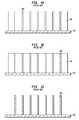
- Metal nanowireshave been conventionally formed by a bottom-up ECD or electroplating through mask process, as shown in FIGS. 1A-1C .
- a substrate structurecomprising a supporting matrix 100 with one or more open pores 104 and a conductive base layer 102 is first provided, as shown in FIG. 1A .
- Each of the open pores 104extends through the supporting matrix 100 onto the conductive base layer 102 .
- An ECD or electroplating processis then carried out to deposit a metal material 106 over the conductive base layer 102 and to fill the open pores 104 , as shown in FIG. 1B .
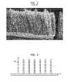
- FIG. 2is a picture of multiple metal nanowires formed by such a conventional bottom-up ECD process.
- compositionally modulated structuresthat comprise alternating layers of ferromagnetic materials and nonmagnetic materials, such as Co/Cu, Co/Ru, Co/Au, Ni/Cu, NiCo/Cu, NiFe/Cu, CoFe/Cu, FeCoNi/Cu, etc.
- Such compositionally modulated ferromagnetic-nonmagnetic structuresare particularly useful in giant magnetoresistance (GMR) applications, which require alternating layers of ferromagnetic and non-magnetic materials.
- GMRgiant magnetoresistance
- the conventional bottom-up electrodeposition of the above ferromagnetic/nonmagnetic layered structuresrelies on the large difference between the reversible potentials of the ferromagnetic/nonmagnetic materials.
- the nonmagnetic elementssuch as Cu and Au
- the ferromagnetic elementssuch as Fe, Ni and Co.
- the nonmagnetic elementsare electrodeposited at a much less negative potential than the ferromagnetic elements.
- the nonmagnetic and ferromagnetic elementsdo not interact with each other during electrodeposition.
- an electrolyte with a small amount of nonmagnetic elements and an excess amount of ferromagnetic elementsis generally used to form the ferromagnetic/nonmagnetic layered structures.
- pure elemental nonmagnetic materialis electrochemically deposited, while the ferromagnetic elements are not deposited.
- both the nonmagnetic and the ferromagnetic elementsare electrochemically deposited. Due to the small amount of nonmagnetic species available in the solution, the ferromagnetic elements are deposited at a much faster rate than the nonmagnetic elements, thereby resulting in a deposited layer with ferromagnetic characteristics.
- the conventional bottom-up ECD processhas never been used for forming compositionally modulated structures that comprise alternative layers of different ferromagnetic materials, which have very close reversible potentials and which may interact with each other during electrodeposition.
- the present inventionrelates to a method comprising:
- the at least one open porehas a cross-sectional diameter ranging from about 10 nm to about 1000 nm.
- the electroplating solutioncomprises a first ferromagnetic metal element and a second, different ferromagnetic metal element.
- Some of the resulting ferromagnetic layersmay comprise the first (but not the second) ferromagnetic metal element, and others of the resulting ferromagnetic layers may comprise the second (but not the first) ferromagnetic metal element.
- all of the deposited ferromagnetic layerscomprise the first and second ferromagnetic metal elements, but in different proportions.
- the electroplating solutioncomprises a ferromagnetic metal element and a non-ferromagnetic metal element.
- the resulting ferromagnetic layersare ferromagnetic and all comprise the ferromagnetic metal element and the non-ferromagnetic metal element, but in different proportions.
- the electroplating solutioncomprises a ferromagnetic metal element, a first non-ferromagnetic metal element, and a second, different non-ferromagnetic metal element.
- Some of the resulting ferromagnetic layerscomprise the ferromagnetic metal element alloyed with the first (but not the second) non-ferromagnetic metal element, and others of the resulting ferromagnetic layers comprise the ferromagnetic metal element alloyed with the second (but not the first) non-ferromagnetic metal element.
- potential pulses with multiple high and/or low potential valuescan be applied, and the at least one open pore in the substrate matrix may be filled with alternating ferromagnetic layers of more than two different material compositions.
- the different material compositionsmay contain different ferromagnetic elements, different non-ferromagnetic elements, same ferromagnetic elements at different proportions, or same ferromagnetic and non-ferromagnetic elements at different proportions.
- the electroplating solutioncomprises a Ni salt and a Fe salt, so that the resulting first and second ferromagnetic layers both comprise Ni—Fe alloys but with different proportions of Ni and Fe.
- the supporting matrix as described hereinabovemay comprise any suitable materials, e.g., photoresists, e-beam or x-ray dielectric resist materials, etc., which can be patterned to form open pores therein.
- the supporting matrixcomprises a material selected from the group consisting of Si, SiO 2 , Si 3 N 4 , Al, Al 2 O 3 , and mixtures thereof.
- the conductive base layermay comprise any material that is conductive, such as metals, metal alloys, metal suicides, metal nitrides, doped semiconductors, etc.
- the conductive base layercomprises a material selected from the group consisting of Au, Cu, Pt, Pd, Ag, Si, GaAs, and alloys thereof.
- the pulsed electroplating potential as described hereinabovemay have high pulses ranging from about ⁇ 1.0 V to about ⁇ 1.8 V (as measured against a saturated calomel electrode or SCE) and low pulses ranging from ⁇ 0.3 V to about ⁇ 1.4 V (as measured against the SCE), provided that a high potential pulse always has a potential higher than those of the preceding and subsequent low potential pulses.
- the pulsed electroplating potentialcan comprise high and/or low pulses of more than two potential values, so that the nanostructure formed comprises alternating ferromagnetic layers of more than two different material compositions.
- the pulsed electroplating potentialcan comprise continuous changes, as discussed in more detail hereinafter, so that the nanostructure formed comprises continuous and gradual compositional changes.
- the method of the present inventionmay further comprise the step of magnetizing the alternating ferromagnetic layers to form a plurality of alternating magnetic domains of opposite directions that are separated from each other by domain walls located therebetween. Such magnetic domains and domain walls are movable across the alternating ferromagnetic layers upon application of a driving current. In this manner, a magnetic storage device is formed, in which data can be stored as the magnetization of magnetic domains and the presence of domain walls.
- the present inventionrelates to a nanostructure having a cross-sectional diameter ranging from about 10 nm to about 1000 nm and comprising a plurality of alternating ferromagnetic layers of different material compositions.
- some of the ferromagnetic layersmay comprise a first ferromagnetic metal element, and others of the second ferromagnetic layers may comprise a second, different ferromagnetic metal element.
- the alternating ferromagnetic layersmay both comprise the first and second, different ferromagnetic metal elements, but in different proportions.
- some of the ferromagnetic layersmay comprise a ferromagnetic metal element alloyed with a first non-ferromagnetic metal element, and others of the ferromagnetic layers may comprise the same ferromagnetic metal element alloyed with a second, different non-ferromagnetic metal element. Still further, the alternating ferromagnetic layers may comprise the same ferromagnetic and non-ferromagnetic metal elements, but in different proportions.
- the first and second ferromagnetic layersboth comprise Ni—Fe alloys but with different proportions of Ni and Fe.
- the nanostructure of the present inventionmay further comprise a plurality of alternating magnetic domains of opposite directions that are separated from each other by domain walls located therebetween. Such magnetic domains and domain walls are movable across the first and second ferromagnetic layers upon application of a driving current. Therefore, the nanostructure of the present invention can function as a magnetic storage device, in which data can be stored as the magnetization of magnetic domains and the presence of domain walls.
- FIGS. 1A-1Care cross-sectional views that illustrate the processing steps of a conventional bottom-up ECD or electroplating through mask process for forming metal nanowires.
- FIG. 2is a pictorial view of multiple metal nanowires formed by the conventional bottom-up ECD process.
- FIG. 3is a cross-sectional view of compositionally modulated nanostructures comprising alternating first and second ferromagnetic layers of different material compositions, according to one embodiment of the present invention.
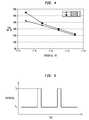
- FIG. 4is a graph that plots the Fe contents of Ni—Fe alloys as deposited from two different Ni—Fe electroplating solutions as a function of the applied electroplating potentials.
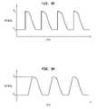
- FIG. 5shows the potential profile of a pulsed electroplating potential that comprises abruptly alternating high and low pulses, according to one embodiment of the present invention.
- FIGS. 6A and 6Bshow scanning electron microscopy (SEM) pictures of ferromagnetic nanowires that contain alternating layers of Ni 45 Fe 55 and Ni 80 Fe 20 alloys, as electroplated using a pulsed potential with a potential profile similar to that shown in FIG. 5 , according to one embodiment of the present invention.
- the wiresare shown after being etched in an acid solution to selectively remove the Ni 45 Fe 55 alloy.
- the thicker sections of the wirecontain the Ni 80 Fe 20 alloy, and the thinner sections of the wire contain the Ni 45 Fe 55 alloy.
- FIG. 7shows the potential profile of a pulsed electroplating potential that comprises alternating high and low pulses with a ramping period therebetween, according to one embodiment of the present invention.
- FIG. 8shows SEM pictures of ferromagnetic nanowires that contain alternating layers of Ni 45 Fe 55 and Ni 80 Fe 20 alloys, as electroplated using a pulsed potential with a potential profile similar to that shown in FIG. 7 , according to one embodiment of the present invention.
- the wiresare shown after being etched in an acid solution to selectively remove the Ni 45 Fe 55 alloy.
- the thicker sections of the wirecontain the Ni 80 Fe 20 alloy, and the notched sections of the wire contain the Ni 45 Fe 55 alloy.
- FIGS. 9A-9Hshow various exemplary pulsed electroplating potentials of different potential profiles.
- ferromagnetic materialrefers to any material that can be magnetized by applying an external magnetic field and exhibit remnant magnetization after the external magnetic field is removed.
- ferromagnetic layeror “ferromagnetic layers” as used herein refers to one or more layered structures that exhibit spontaneous magnetization overall.
- the ferromagnetic layer or layers of the present inventioncomprise(s) at least one ferromagnetic element, with or without additional ferromagnetic or non-ferromagnetic elements.
- the present inventionprovides compositionally modulated ferromagnetic nanostructures that each has a cross-sectional diameter ranging from about 10 nm to about 1000 nm and comprises alternating ferromagnetic layers of different material properties.
- the present inventionis also broadly applicable to film structures comprising alternating ferromagnetic layers of different material properties.
- Such ferromagnetic nanostructurescan be magnetized to form a plurality of alternating magnetic domains of opposite directions with domain walls located therebetween.
- the magnetic domains and domain wallsare movable across the ferromagnetic layers, and the alternating ferromagnetic layers of different material properties are particularly effective in pinning the domain walls and ensuring movement of the domain walls at very discrete and precise increments or steps, without any drifting.
- the ferromagnetic nanostructurescan be used as memory storage devices, in which data is stored as locations of the magnetic domains and domain walls.
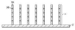
- FIG. 3shows a cross-sectional view of multiple ferromagnetic nanowires 14 located on conductive base layer 12 , each of which has a cross-sectional diameter ranging from about 10 nm to about 1000 nm and contains alternating first and second ferromagnetic layers 14 A and 14 B of different material compositions.
- each of the first ferromagnetic layers 14 Acontains a first ferromagnetic material A
- each of the second ferromagnetic layers 14 Bcontains a second, different ferromagnetic material B.
- the first and second ferromagnetic layers 14 A and 14 Bboth comprise the first ferromagnetic material A and the second, different ferromagnetic material B, but in different proportions.
- each the first ferromagnetic layers 14 Acontains a ferromagnetic material A mixed with a first non-ferromagnetic material C
- each of the second ferromagnetic layers 14 Acontains a ferromagnetic material A mixed with a second, different non-ferromagnetic material D, provided that such non-ferromagnetic materials C and D do not affect the overall ferromagnetic characteristic of layers 14 A and 14 B.
- the first and second ferromagnetic layers 14 A and 14 Bboth comprise a ferromagnetic material A mixed with a non-ferromagnetic material C, but in different proportions, provided that such non-ferromagnetic material C does not affect the overall ferromagnetic characteristic of layers 14 A and 14 B.
- the ferromagnetic materials A and B as disclosed hereinabovemay comprise any suitable ferromagnetic element(s).
- the ferromagnetic materials A and Bmay comprise one or more ferromagnetic elements, including, but not limited to: Fe, Ni, Co, Gd, Dy, Th, Ho, Er, and mixtures or combinations thereof.
- Such ferromagnetic materials A and Bcan present either in pure form, or as mixtures with other ferromagnetic or non-ferromagnetic elements.
- the non-ferromagnetic materials C and D as disclosed hereinabovemay comprise any non-ferromagetic element(s) or mixtures thereof, including, but not limited to: Ru, Mo, Mn, Cr, Si, Ge, Ga, As, Cu, Rh, Pt, Au, Pd, etc.
- the ferromagnetic nanowires of FIG. 3can be magnetized in small sections to form alternating magnetic domains of opposite directions and domain walls located therebetween.
- the magnetic domains and domain wallscan be moved upon the application of a driving current.
- the ferromagnetic nanowiresfunction as memory storage devices, in which digital data is stored as the magnetization of each magnetic domain in each segment, 14 A, and the domain walls between adjacent magnetic domains can be pinned in the segments, 14 B.
- Informationcan then be read from or be written to such a memory storage device by a reading or a writing device when the magnetic domains are moved across such a reading or writing device upon application of a driving current.
- the ferromagnetic nanostructures of the present inventionmay have any regular or irregular cross-sectional shape, such as circular, square, rectangular, triangular, polygonal, semi-circular, ellipsoidal, etc. Further, the ferromagnetic nanostructures of the present invention may be either solid nanorods with relatively homogeneous interior and exterior compositions, or tubular nanostructures with insulating or highly resistive semiconductor cores that are non-magnetic.
- the ferromagnetic nanostructures as shown in FIG. 3comprise only two different ferromagnetic layers, it is understood that the ferromagnetic nanostructures of the present invention can comprise more than two different layers, i.e., additional layers of different material compositions can be provided between the alternating first and second ferromagnetic layers 14 A and 14 B, and such additional layers can be either ferromagnetic or non-ferromagnetic.
- the ferromagnetic nanowires as described hereinabovecan be formed by a pulsed ECD process. Specifically, a substrate containing a supporting matrix with at least one open pore and a conductive base layer 12 is first formed.
- the supporting matrixmay comprise any suitable material, including, but not limited to: Si, SiO 2 , Si 3 N 4 , Al, Al 2 O 3 , and mixtures thereof. Therefore, the open pore preferably has a cross-sectional diameter from about 10 nm to about 1000 nm. Further, the open pore preferably extends through the supporting matrix onto the conductive base layer, so that the conductive base layer can be used as a seed layer for subsequent electroplating.
- the shape of the open poredetermines the shape of the ferromagnetic nanowires to be formed.
- the conductive base layermay comprise any suitable conductive material for electroplating, which includes, but is not limited to: Au, Cu, Pt, Ag, Si, GaAs, and alloys thereof.
- anodized Al 2 O 3 film or commercially available Whatman® membrane(manufactured by Whatman, Inc. at Florham Park, N.J.), which contains a supporting matrix of aluminum oxide with open pores therein, can be used for forming the substrate of the present application by sputtering a metal on one side of the membrane to form the conductive base layer.
- Electroplating of the above-described substrate structureis then carried out in an electroplating solution under a pulsed electroplating potential, so as to form alternating ferromagnetic layers of different material compositions. Subsequently, the supporting matrix is selectively removed to form the desired ferromagnetic nanostructures.
- the electroplating solution as used hereincomprises one or more salts of ferromagnetic metal species and one or more supporting electrolyte salts.
- the electroplating solutionmay further comprise one or more components, such as pH buffering agents, complexing agents, surfactants, organic additives (e.g., brighteners or suppressants), etc., for enhancing the material quality of the deposited layers.
- the electroplating solutionmay comprise a first salt of a first ferromagnetic metal element and at least one additional salt of a second, different ferromagnetic metal element, which can be used to form alternating ferromagnetic layers that comprise different ferromagnetic metal elements, or ferromagnetic layers that comprise the same ferromagnetic metal elements but in different proportions.
- the electroplating solutionmay comprise a salt of a ferromagnetic metal element and at least one additional salt of a non-ferromagnetic metal element, which can be used to form alternating ferromagnetic layers that comprise both the ferromagnetic metal element and the non-ferromagnetic metal element but in different proportions.
- the electroplating solutionmay comprise a salt of a ferromagnetic metal element, a first additional salt of a first non-ferromagnetic metal element, and a second additional salt of a second, different non-ferromagnetic metal element, which can be used to form alternating ferromagnetic layers that comprise the same ferromagnetic metal element mixed with different non-ferromagnetic metal elements.
- An exemplary electroplating solutioncomprises about 0.05-0.5 mol/L nickel sulfate, 0.1-1 mol/L nickel chloride, 0.005-0.2 mol/L ferrous sulfate, 0.1-0.5 mol/L boric acid, 0.1-1 mol/L sodium chloride, and 0.1-2 g/L sodium saccharin, and 0.05-0.1 g/L sodium lauryl sulfate, which can be used to form alternating ferromagnetic layers that comprise Ni—Fe alloys with different Ni and Fe contents.
- FIG. 4shows the change of Fe contents in electroplated Ni—Fe alloys in response to the change of electroplating potentials. Specifically, under a relatively low electroplating potential of about ⁇ 1.3V (as measured against the SCE), the Fe content in the Ni—Fe alloys electroplated from solutions 1 and 2 ranges from about 40% to about 55%. However, under a relatively high electroplating potential of about ⁇ 1.6V (as measured against the SCE), the Fe content reduces to about 20%.
- alternating ferromagnetic layers with different material compositionscan be formed using the same electroplating solution in a continuous electroplating process.
- the thicknesses of the alternating ferromagnetic layerscan be precisely controlled by duration of each potential pulse.
- FIG. 5shows the potential profile for an exemplary pulsed electroplating potential that can be used in the present invention.
- the pulsed electroplating potentialcomprises low pulses of potential value E 1 and high pulses of potential value E 2 , while the high and low pulses abruptly alternate from one to the other over time.
- the high pulseshave potential values ranging from about ⁇ 1.0 V to about ⁇ 1.8 V (as measured against the SCE), and the low pulses have potential values ranging from about ⁇ 0.3 V to about ⁇ 1.4 V (as measured against the SCE).
- FIG. 6Ashows a SEM picture of ferromagnetic nanowires that contain alternating layers of Ni 45 Fe 55 and Ni 80 Fe 20 , as electroplated from the exemplary electroplating solution as described hereinabove using a pulsed electroplating potential with a potential profile similar to that shown in FIG. 5 .
- the high pulseshave a potential value of about ⁇ 1.6V
- the low pulseshave a potential value of ⁇ 1.3V, with respect to a saturated calomel reference electrode.
- the Al 2 O 3 matrixwas dissolved in a NaOH solution, and the wires were etched in a HNO 3 ethanol solution before imaging.
- FIG. 6Bis an enlarged picture of the region circled by white in FIG. 6A .
- the Ni 45 Fe 55 layers as shown in FIG. 6Bhave a layer thickness of about 400 nm, and the Ni 80 Fe 20 layers have a layer thickness of about 200 nm.
- FIG. 7shows the potential profile for another exemplary pulsed electroplating potential that can be used in the present invention.
- the pulsed electroplating potentialcomprises alternating low pulses of potential value E 1 and high pulses of potential value E 2 , while a ramping period (T) is provided between E 1 and E 2 .
- the composition of the electroplated layerscan be more continuously and gradually controlled with such a ramping period.
- FIG. 8shows the SEM pictures of ferromagnetic nanowires that contain alternating layers of Ni 45 Fe 55 and Ni 80 Fe 20 , as electroplated using a pulsed electroplating potential with a potential profile similar to that shown in FIG. 7 .
- the pulsed electroplating potentialmay have any suitable potential profile, as long as such potential profile contains alternating high and low pulses.
- additional potential profiles as shown in FIGS. 9A-9Hcan also be used for forming the ferromagnetic nanostructures of the present invention.
- the pulsed electroplating currentcan comprise high pulses of different potential values or low pulses of different potential values or both, so that the nanostructure so formed comprises additional layers of different material compositions between the first and second ferromagnetic layers.
- the present inventionbroadly covers any ferromagnetic nanostructure with alternating ferromagnetic layers of different material compositions.
- the number of alternating ferromagnetic layersmay range from two to hundreds.
- each ferromagnetic layermay comprise any ferromagnetic elements mixed with any number of additional ferromagnetic or non-ferromagnetic elements, as long as the overall characteristic of such a layer remains ferromagnetic.
- the ferromagnetic nanostructures of the present inventioncan be used for forming memory storage elements, as described hereinabove, or any other spinstronic devices that require alternating ferromagnetic layers of different material compositions.
Landscapes
- Chemical & Material Sciences (AREA)
- Engineering & Computer Science (AREA)
- Chemical Kinetics & Catalysis (AREA)
- Electrochemistry (AREA)
- Materials Engineering (AREA)
- Metallurgy (AREA)
- Organic Chemistry (AREA)
- Power Engineering (AREA)
- Crystallography & Structural Chemistry (AREA)
- Nanotechnology (AREA)
- Manufacturing & Machinery (AREA)
- Inorganic Chemistry (AREA)
- Electroplating Methods And Accessories (AREA)
- Thin Magnetic Films (AREA)
- Semiconductor Memories (AREA)
- Mram Or Spin Memory Techniques (AREA)
- Hall/Mr Elements (AREA)
Abstract
Description
- forming a substrate structure comprising a supporting matrix having at least one open pore extending therethrough onto a conductive base layer; and
- electroplating the substrate structure by immersing the substrate structure in an electroplating solution that comprises at least one ferromagnetic metal element and one or more additional, different metal elements, either magnetic or nonmagnetic, and applying a pulsed electroplating potential with alternating pulses to the conductive base layer of the substrate structure to deposit a plurality of alternating ferromagnetic layers of different material compositions in the at least one open pore of the supporting matrix.
Claims (8)
Priority Applications (7)
| Application Number | Priority Date | Filing Date | Title |
|---|---|---|---|
| US11/620,480US7736753B2 (en) | 2007-01-05 | 2007-01-05 | Formation of nanostructures comprising compositionally modulated ferromagnetic layers by pulsed ECD |
| PCT/US2007/020646WO2008130371A1 (en) | 2007-01-05 | 2007-09-25 | Formation of nanostructures comprising compositionally modulated ferromagnetic layers by pulsed ecd |
| CN2007800480505ACN101681706B (en) | 2007-01-05 | 2007-09-25 | Nanostructures and methods of forming them |
| KR1020097012294AKR20090095591A (en) | 2007-01-05 | 2007-09-25 | Formation of nanostructures comprising compositionally modulated ferromagnetic layers by pulsed ecd |
| JP2009544828AJP2010515820A (en) | 2007-01-05 | 2007-09-25 | Formation of nanostructures containing compositionally modulated ferromagnetic layers by pulsed ECD |
| EP07874503AEP2118914A4 (en) | 2007-01-05 | 2007-09-25 | Formation of nanostructures comprising compositionally modulated ferromagnetic layers by pulsed ecd |
| US12/540,710US20090301890A1 (en) | 2007-01-05 | 2009-08-13 | Formation of nanostructures comprising compositionally modulated ferromagnetic layers by pulsed ecd |
Applications Claiming Priority (1)
| Application Number | Priority Date | Filing Date | Title |
|---|---|---|---|
| US11/620,480US7736753B2 (en) | 2007-01-05 | 2007-01-05 | Formation of nanostructures comprising compositionally modulated ferromagnetic layers by pulsed ECD |
Related Child Applications (1)
| Application Number | Title | Priority Date | Filing Date |
|---|---|---|---|
| US12/540,710DivisionUS20090301890A1 (en) | 2007-01-05 | 2009-08-13 | Formation of nanostructures comprising compositionally modulated ferromagnetic layers by pulsed ecd |
Publications (2)
| Publication Number | Publication Date |
|---|---|
| US20080166584A1 US20080166584A1 (en) | 2008-07-10 |
| US7736753B2true US7736753B2 (en) | 2010-06-15 |
Family
ID=39594557
Family Applications (2)
| Application Number | Title | Priority Date | Filing Date |
|---|---|---|---|
| US11/620,480Expired - Fee RelatedUS7736753B2 (en) | 2007-01-05 | 2007-01-05 | Formation of nanostructures comprising compositionally modulated ferromagnetic layers by pulsed ECD |
| US12/540,710AbandonedUS20090301890A1 (en) | 2007-01-05 | 2009-08-13 | Formation of nanostructures comprising compositionally modulated ferromagnetic layers by pulsed ecd |
Family Applications After (1)
| Application Number | Title | Priority Date | Filing Date |
|---|---|---|---|
| US12/540,710AbandonedUS20090301890A1 (en) | 2007-01-05 | 2009-08-13 | Formation of nanostructures comprising compositionally modulated ferromagnetic layers by pulsed ecd |
Country Status (6)
| Country | Link |
|---|---|
| US (2) | US7736753B2 (en) |
| EP (1) | EP2118914A4 (en) |
| JP (1) | JP2010515820A (en) |
| KR (1) | KR20090095591A (en) |
| CN (1) | CN101681706B (en) |
| WO (1) | WO2008130371A1 (en) |
Cited By (16)
| Publication number | Priority date | Publication date | Assignee | Title |
|---|---|---|---|---|
| US20110236260A1 (en)* | 2010-03-25 | 2011-09-29 | The Industry & Academic Cooperation In Chungnam National University | Digital Barcode Nano-Wire and System for Bio-Sensing Using the Same |
| US10781524B2 (en) | 2014-09-18 | 2020-09-22 | Modumetal, Inc. | Methods of preparing articles by electrodeposition and additive manufacturing processes |
| US10808322B2 (en)* | 2013-03-15 | 2020-10-20 | Modumetal, Inc. | Electrodeposited compositions and nanolaminated alloys for articles prepared by additive manufacturing processes |
| US10844504B2 (en) | 2013-03-15 | 2020-11-24 | Modumetal, Inc. | Nickel-chromium nanolaminate coating having high hardness |
| US10961635B2 (en) | 2005-08-12 | 2021-03-30 | Modumetal, Inc. | Compositionally modulated composite materials and methods for making the same |
| US11118280B2 (en) | 2013-03-15 | 2021-09-14 | Modumetal, Inc. | Nanolaminate coatings |
| US11180864B2 (en) | 2013-03-15 | 2021-11-23 | Modumetal, Inc. | Method and apparatus for continuously applying nanolaminate metal coatings |
| US11242613B2 (en) | 2009-06-08 | 2022-02-08 | Modumetal, Inc. | Electrodeposited, nanolaminate coatings and claddings for corrosion protection |
| US11286575B2 (en) | 2017-04-21 | 2022-03-29 | Modumetal, Inc. | Tubular articles with electrodeposited coatings, and systems and methods for producing the same |
| US11293272B2 (en) | 2017-03-24 | 2022-04-05 | Modumetal, Inc. | Lift plungers with electrodeposited coatings, and systems and methods for producing the same |
| US11365488B2 (en) | 2016-09-08 | 2022-06-21 | Modumetal, Inc. | Processes for providing laminated coatings on workpieces, and articles made therefrom |
| US11519093B2 (en) | 2018-04-27 | 2022-12-06 | Modumetal, Inc. | Apparatuses, systems, and methods for producing a plurality of articles with nanolaminated coatings using rotation |
| US11692281B2 (en) | 2014-09-18 | 2023-07-04 | Modumetal, Inc. | Method and apparatus for continuously applying nanolaminate metal coatings |
| US12076965B2 (en) | 2016-11-02 | 2024-09-03 | Modumetal, Inc. | Topology optimized high interface packing structures |
| US12077876B2 (en) | 2016-09-14 | 2024-09-03 | Modumetal, Inc. | System for reliable, high throughput, complex electric field generation, and method for producing coatings therefrom |
| US12227869B2 (en) | 2016-09-09 | 2025-02-18 | Modumetal, Inc. | Application of laminate and nanolaminate materials to tooling and molding processes |
Families Citing this family (25)
| Publication number | Priority date | Publication date | Assignee | Title |
|---|---|---|---|---|
| US7768809B2 (en)* | 2008-10-02 | 2010-08-03 | International Business Machines Corporation | Wall nucleation propagation for racetrack memory |
| US8449948B2 (en)* | 2009-09-10 | 2013-05-28 | Western Digital (Fremont), Llc | Method and system for corrosion protection of layers in a structure of a magnetic recording transducer |
| KR101161060B1 (en)* | 2009-11-30 | 2012-06-29 | 서강대학교산학협력단 | Arranging apparatus into columnar structure for nano particles and Method for arranging the same |
| JP5424406B2 (en)* | 2010-02-09 | 2014-02-26 | 国立大学法人 長崎大学 | Compound semiconductor fine wire manufacturing method and compound semiconductor fine wire assembly |
| CN103827986B (en) | 2011-08-17 | 2017-02-15 | 明尼苏达大学董事会 | Iron nitride permanent magnet and technique for forming iron nitride permanent magnet |
| CA2899827C (en) | 2013-02-07 | 2016-08-23 | Jian-Ping Wang | Iron nitride permanent magnet and technique for forming iron nitride permanent magnet |
| EP3014637A4 (en) | 2013-06-27 | 2017-05-03 | Regents of the University of Minnesota | Iron nitride materials and magnets including iron nitride materials |
| CN103409780B (en)* | 2013-08-13 | 2016-01-20 | 山东大学 | A kind of method of nano-porous gold being carried out to surface alloy modification |
| JP2017517630A (en) | 2014-03-28 | 2017-06-29 | リージェンツ オブ ザ ユニバーシティ オブ ミネソタ | Iron Nitride Magnetic Material Containing Coated Nanoparticles |
| US9994949B2 (en) | 2014-06-30 | 2018-06-12 | Regents Of The University Of Minnesota | Applied magnetic field synthesis and processing of iron nitride magnetic materials |
| US10002694B2 (en) | 2014-08-08 | 2018-06-19 | Regents Of The University Of Minnesota | Inductor including alpha″-Fe16Z2 or alpha″-Fe16(NxZ1-x)2, where Z includes at least one of C, B, or O |
| US10072356B2 (en) | 2014-08-08 | 2018-09-11 | Regents Of The University Of Minnesota | Magnetic material including α″-Fe16(NxZ1-x)2 or a mixture of α″-Fe16Z2 and α″-Fe16N2, where Z includes at least one of C, B, or O |
| KR20170039741A (en) | 2014-08-08 | 2017-04-11 | 리전츠 오브 더 유니버시티 오브 미네소타 | Multilayer iron nitride hard magnetic materials |
| JP2017532439A (en) | 2014-08-08 | 2017-11-02 | リージェンツ オブ ザ ユニバーシティ オブ ミネソタ | Formation of iron nitride hard magnetic materials using chemical vapor deposition or liquid phase epitaxy |
| JP6631029B2 (en)* | 2015-04-21 | 2020-01-15 | Tdk株式会社 | Permanent magnet and rotating machine having the same |
| CN105887148A (en)* | 2016-06-03 | 2016-08-24 | 河海大学 | Ni-B/SiC CMMA coating for marine equipment and preparation method thereof |
| CN106011955A (en)* | 2016-06-03 | 2016-10-12 | 河海大学 | A corrosion-resistant and wear-resistant Ni-W/Al2O3 CMMA protective layer for marine engineering machinery and its preparation method |
| CN106011956A (en)* | 2016-06-03 | 2016-10-12 | 河海大学 | Electrochemical preparation method for CMMA structure capable of improving corrosion resistance of Ni-W alloy |
| CN105908227A (en)* | 2016-06-03 | 2016-08-31 | 河海大学 | Electrochemical preparation method for CMMA structure capable of improving corrosion resistance and abrasion resistance of Ni-B alloy |
| CN105908228A (en)* | 2016-06-03 | 2016-08-31 | 河海大学 | Nickel alloy composition modulated multilayer alloy (CMMA) coating and preparation method thereof |
| US11377749B1 (en) | 2017-10-17 | 2022-07-05 | Seagate Technology Llc | Electrodeposition of high damping magnetic alloys |
| US11152020B1 (en) | 2018-05-14 | 2021-10-19 | Seagate Technology Llc | Electrodeposition of thermally stable alloys |
| CN109795975A (en)* | 2018-12-28 | 2019-05-24 | 南京大学 | A kind of metal micro-/ nano linear array and preparation method thereof |
| US12018386B2 (en) | 2019-10-11 | 2024-06-25 | Regents Of The University Of Minnesota | Magnetic material including α″-Fe16(NxZ1-x)2 or a mixture of α″-Fe16Z2 and α″-Fe16N2, where Z includes at least one of C, B, or O |
| KR20220124787A (en)* | 2020-01-10 | 2022-09-14 | 램 리써치 코포레이션 | Improved TSV process window and fill performance by long pulsing and ramping |
Citations (6)
| Publication number | Priority date | Publication date | Assignee | Title |
|---|---|---|---|---|
| US6177204B1 (en)* | 1995-11-06 | 2001-01-23 | Motorola, Inc. | Ferromagnetic GMR material and method of forming and using |
| US20020031008A1 (en) | 2000-09-08 | 2002-03-14 | Tohru Den | Magnetic device and method for manufacturing the same, and solid magnetic memory |
| US6741019B1 (en)* | 1999-10-18 | 2004-05-25 | Agere Systems, Inc. | Article comprising aligned nanowires |
| US20050168879A1 (en)* | 2001-09-17 | 2005-08-04 | Headway Technologies, Inc. | Multilayered structures comprising magnetic nano-oxide layers for current perpendicular to plane GMR heads |
| US20050186686A1 (en) | 2004-02-25 | 2005-08-25 | International Business Machines Corporation | Method of fabricating data tracks for use in a magnetic shift register memory device |
| US20080165576A1 (en)* | 2007-01-05 | 2008-07-10 | International Business Machines Corporation | Memory storage devices comprising different ferromagnetic material layers, and methods of making and using the same |
Family Cites Families (14)
| Publication number | Priority date | Publication date | Assignee | Title |
|---|---|---|---|---|
| US3866192A (en)* | 1973-03-01 | 1975-02-11 | Honeywell Inc | Plated wire memory element |
| JP2544845B2 (en)* | 1990-08-23 | 1996-10-16 | インターナショナル・ビジネス・マシーンズ・コーポレイション | Magnetic thin film, laminate, magnetic recording head, magnetic shield, and method for producing laminate |
| SE9903531D0 (en)* | 1999-09-30 | 1999-09-30 | Res Inst Acreo Ab | Method for electro-deposition of metallic multi-layers |
| US20040209376A1 (en)* | 1999-10-01 | 2004-10-21 | Surromed, Inc. | Assemblies of differentiable segmented particles |
| JP2002084019A (en)* | 2000-09-08 | 2002-03-22 | Canon Inc | Magnetic device and solid-state magnetic memory |
| US6937446B2 (en)* | 2000-10-20 | 2005-08-30 | Kabushiki Kaisha Toshiba | Magnetoresistance effect element, magnetic head and magnetic recording and/or reproducing system |
| JP3833512B2 (en)* | 2000-10-20 | 2006-10-11 | 株式会社東芝 | Magnetoresistive effect element |
| US6776891B2 (en)* | 2001-05-18 | 2004-08-17 | Headway Technologies, Inc. | Method of manufacturing an ultra high saturation moment soft magnetic thin film |
| JP3708856B2 (en)* | 2001-09-07 | 2005-10-19 | アルプス電気株式会社 | Soft magnetic film, thin film magnetic head using soft magnetic film, method for manufacturing soft magnetic film, and method for manufacturing thin film magnetic head |
| US7569131B2 (en)* | 2002-08-12 | 2009-08-04 | International Business Machines Corporation | Method for producing multiple magnetic layers of materials with known thickness and composition using a one-step electrodeposition process |
| US7108797B2 (en)* | 2003-06-10 | 2006-09-19 | International Business Machines Corporation | Method of fabricating a shiftable magnetic shift register |
| CN100410166C (en)* | 2004-08-13 | 2008-08-13 | 清华大学 | Preparation method of magnetic field-induced growth magnetic one-dimensional nanowire array |
| CN100431188C (en)* | 2005-06-09 | 2008-11-05 | 上海交通大学 | Fabrication method of magnetosensitive device based on giant magnetoimpedance effect of soft magnetic multilayer film |
| US20080156654A1 (en)* | 2006-08-08 | 2008-07-03 | Joseph Wang | Identification Based On Compositionally Encoded Nanostructures |
- 2007
- 2007-01-05USUS11/620,480patent/US7736753B2/ennot_activeExpired - Fee Related
- 2007-09-25WOPCT/US2007/020646patent/WO2008130371A1/enactiveSearch and Examination
- 2007-09-25JPJP2009544828Apatent/JP2010515820A/enactivePending
- 2007-09-25EPEP07874503Apatent/EP2118914A4/ennot_activeWithdrawn
- 2007-09-25CNCN2007800480505Apatent/CN101681706B/ennot_activeExpired - Fee Related
- 2007-09-25KRKR1020097012294Apatent/KR20090095591A/ennot_activeAbandoned
- 2009
- 2009-08-13USUS12/540,710patent/US20090301890A1/ennot_activeAbandoned
Patent Citations (6)
| Publication number | Priority date | Publication date | Assignee | Title |
|---|---|---|---|---|
| US6177204B1 (en)* | 1995-11-06 | 2001-01-23 | Motorola, Inc. | Ferromagnetic GMR material and method of forming and using |
| US6741019B1 (en)* | 1999-10-18 | 2004-05-25 | Agere Systems, Inc. | Article comprising aligned nanowires |
| US20020031008A1 (en) | 2000-09-08 | 2002-03-14 | Tohru Den | Magnetic device and method for manufacturing the same, and solid magnetic memory |
| US20050168879A1 (en)* | 2001-09-17 | 2005-08-04 | Headway Technologies, Inc. | Multilayered structures comprising magnetic nano-oxide layers for current perpendicular to plane GMR heads |
| US20050186686A1 (en) | 2004-02-25 | 2005-08-25 | International Business Machines Corporation | Method of fabricating data tracks for use in a magnetic shift register memory device |
| US20080165576A1 (en)* | 2007-01-05 | 2008-07-10 | International Business Machines Corporation | Memory storage devices comprising different ferromagnetic material layers, and methods of making and using the same |
Non-Patent Citations (6)
| Title |
|---|
| Alper, M. et al., Giant Magnetoresistance in Electrodeposited Superlattices, Appl. Phys. Lett, Oct. 11, 1993, pp. 2144-2146, vol. 63, No. 15. |
| Jimbo, Mutsuko, Giant Magnetoresistance in FeNiCO / Cu Multilayers, Jpn. J. Appl. Phys., Sep. 15, 1992, pp. L 1348-L 1350, vol. 31, Part 2, No. 9B. |
| Martin, Charles R., Nanomaterials: A Membrane-Based Synthetic Approach, Science, New Series, Dec. 23, 1994, pp. 1961-1966, vol. 266, No. 5193, downloaded from www.jstor.org. |
| Parkin S. S. P., Oscillations in Giant Magnetoresistance and Antiferromagnetic Coupling in [Ni81Fe19/Cu]N Multilaters, Appl. Phys. Lett., Jan. 27, 1992, pp. 512-514, vol. 60, No. 4. |
| Parkin, S. S. P. et al., Oscillations in Exchange Coupling and Magnetoresistance in Metallic Superlattice Structures: Co/Ru, Co/Cr, and Fe/Cr, The American Physical Society, 1990, pp. 2304-2308, vol. 64, No. 19. |
| Ross, C. A. , Electrodeposited Multilayer Thin Films, Annu. Rev. Mater. Sci., 1994, pp. 159-188, vol. 24, downloaded from arjournals.annualreviews.org. |
Cited By (23)
| Publication number | Priority date | Publication date | Assignee | Title |
|---|---|---|---|---|
| US10961635B2 (en) | 2005-08-12 | 2021-03-30 | Modumetal, Inc. | Compositionally modulated composite materials and methods for making the same |
| US11242613B2 (en) | 2009-06-08 | 2022-02-08 | Modumetal, Inc. | Electrodeposited, nanolaminate coatings and claddings for corrosion protection |
| US20110236260A1 (en)* | 2010-03-25 | 2011-09-29 | The Industry & Academic Cooperation In Chungnam National University | Digital Barcode Nano-Wire and System for Bio-Sensing Using the Same |
| US9011774B2 (en)* | 2010-03-25 | 2015-04-21 | The Industry & Academic Cooperation In Chungnam National University | Digital barcode nano-wire and system for bio-sensing using the same |
| US20210071303A1 (en)* | 2013-03-15 | 2021-03-11 | Modumetal, Inc. | Electrodeposited compositions and nanolaminated alloys for articles prepared by additive manufacturing processes |
| US11851781B2 (en) | 2013-03-15 | 2023-12-26 | Modumetal, Inc. | Method and apparatus for continuously applying nanolaminate metal coatings |
| US10808322B2 (en)* | 2013-03-15 | 2020-10-20 | Modumetal, Inc. | Electrodeposited compositions and nanolaminated alloys for articles prepared by additive manufacturing processes |
| US11118280B2 (en) | 2013-03-15 | 2021-09-14 | Modumetal, Inc. | Nanolaminate coatings |
| US11168408B2 (en) | 2013-03-15 | 2021-11-09 | Modumetal, Inc. | Nickel-chromium nanolaminate coating having high hardness |
| US11180864B2 (en) | 2013-03-15 | 2021-11-23 | Modumetal, Inc. | Method and apparatus for continuously applying nanolaminate metal coatings |
| US12084773B2 (en)* | 2013-03-15 | 2024-09-10 | Modumetal, Inc. | Electrodeposited compositions and nanolaminated alloys for articles prepared by additive manufacturing processes |
| US10844504B2 (en) | 2013-03-15 | 2020-11-24 | Modumetal, Inc. | Nickel-chromium nanolaminate coating having high hardness |
| US11560629B2 (en) | 2014-09-18 | 2023-01-24 | Modumetal, Inc. | Methods of preparing articles by electrodeposition and additive manufacturing processes |
| US11692281B2 (en) | 2014-09-18 | 2023-07-04 | Modumetal, Inc. | Method and apparatus for continuously applying nanolaminate metal coatings |
| US10781524B2 (en) | 2014-09-18 | 2020-09-22 | Modumetal, Inc. | Methods of preparing articles by electrodeposition and additive manufacturing processes |
| US11365488B2 (en) | 2016-09-08 | 2022-06-21 | Modumetal, Inc. | Processes for providing laminated coatings on workpieces, and articles made therefrom |
| US12227869B2 (en) | 2016-09-09 | 2025-02-18 | Modumetal, Inc. | Application of laminate and nanolaminate materials to tooling and molding processes |
| US12077876B2 (en) | 2016-09-14 | 2024-09-03 | Modumetal, Inc. | System for reliable, high throughput, complex electric field generation, and method for producing coatings therefrom |
| US12076965B2 (en) | 2016-11-02 | 2024-09-03 | Modumetal, Inc. | Topology optimized high interface packing structures |
| US11293272B2 (en) | 2017-03-24 | 2022-04-05 | Modumetal, Inc. | Lift plungers with electrodeposited coatings, and systems and methods for producing the same |
| US11286575B2 (en) | 2017-04-21 | 2022-03-29 | Modumetal, Inc. | Tubular articles with electrodeposited coatings, and systems and methods for producing the same |
| US12344956B2 (en) | 2017-04-21 | 2025-07-01 | Modumetal, Inc. | Tubular articles with electrodeposited coatings, and systems and methods for producing the same |
| US11519093B2 (en) | 2018-04-27 | 2022-12-06 | Modumetal, Inc. | Apparatuses, systems, and methods for producing a plurality of articles with nanolaminated coatings using rotation |
Also Published As
| Publication number | Publication date |
|---|---|
| CN101681706B (en) | 2011-11-09 |
| KR20090095591A (en) | 2009-09-09 |
| US20090301890A1 (en) | 2009-12-10 |
| US20080166584A1 (en) | 2008-07-10 |
| EP2118914A1 (en) | 2009-11-18 |
| EP2118914A4 (en) | 2012-01-18 |
| JP2010515820A (en) | 2010-05-13 |
| CN101681706A (en) | 2010-03-24 |
| WO2008130371A1 (en) | 2008-10-30 |
Similar Documents
| Publication | Publication Date | Title |
|---|---|---|
| US7736753B2 (en) | Formation of nanostructures comprising compositionally modulated ferromagnetic layers by pulsed ECD | |
| Um et al. | Fabrication of long-range ordered aluminum oxide and Fe/Au multilayered nanowires for 3-D magnetic memory | |
| US6611034B2 (en) | Magnetic device and solid-state magnetic memory | |
| Pattanaik et al. | Electrodeposition of hard magnetic films and microstructures | |
| Mansouri et al. | Electrodeposition of equiatomic FeNi and FeCo nanowires: Structural and magnetic properties | |
| JP2002084018A (en) | Magnetic device, method of manufacturing the same, and solid-state magnetic memory | |
| Tabakovic et al. | Preparation of metastable CoFeNi alloys with ultra-high magnetic saturation (Bs= 2.4–2.59 T) by reverse pulse electrodeposition | |
| Brankovic et al. | Pulse electrodeposition of 2.4 T Co/sub 37/Fe/sub 63/alloys at nanoscale for magnetic recording application | |
| Sverdlov et al. | The electrodeposition of cobalt–nickel–iron high aspect ratio thick film structures for magnetic MEMS applications | |
| Varea et al. | Ordered arrays of ferromagnetic, compositionally graded Cu 1− x Ni x alloy nanopillars prepared by template-assisted electrodeposition | |
| Gapin et al. | Patterned media based on soft/hard composite nanowire array of Ni/CoPt | |
| Liu et al. | High moment FeCoNi alloy thin films fabricated by pulsed-current electrodeposition | |
| JP2008069447A (en) | Magnetic anodized aluminum oxide with high oxidation resistance and method for manufacturing the same | |
| García-Torres et al. | Preparation and giant magnetoresistance of electrodeposited Co–Ag/Ag multilayers | |
| JP2013147747A (en) | ELECTRODEPOSITION METHOD OF CoFe ALLOY | |
| Péter et al. | Electrodeposition of Co–Cu–Zn/Cu multilayers: influence of anomalous codeposition on the formation of ternary multilayers | |
| Long et al. | Electrodeposition of Sm–Co film with high Sm content from aqueous solution | |
| Liu et al. | Synthesis and magnetic properties of multilayer Ni/Cu and NiFe/Cu nanowires | |
| KR100858507B1 (en) | Method for producing soft magnetic nickel-iron permalloy and soft magnetic permalloy thin film produced thereby | |
| Hayashi et al. | Growth of Co/Cu multilayered thin films by electro‐deposition | |
| JP7233723B2 (en) | Manufacturing method of alloy thin film | |
| JPH0636929A (en) | Plated magnetic thin film and manufacture thereof | |
| Wang et al. | On low-temperature ordering of FePt nanowires | |
| Péter et al. | Magnetic/Non-magnetic Metallic Multilayer Films | |
| Ohgai | Fabrication of Functional Metallic Nanowires Using Electrodeposition Technique |
Legal Events
| Date | Code | Title | Description |
|---|---|---|---|
| AS | Assignment | Owner name:INTERNATIONAL BUSINESS MACHINES CORPORATION, NEW Y Free format text:ASSIGNMENT OF ASSIGNORS INTEREST;ASSIGNORS:DELIGIANNI, HARIKLIA;HUANG, QIANG;ROMANKIW, LUBOMYR T.;REEL/FRAME:018733/0531 Effective date:20060908 Owner name:INTERNATIONAL BUSINESS MACHINES CORPORATION,NEW YO Free format text:ASSIGNMENT OF ASSIGNORS INTEREST;ASSIGNORS:DELIGIANNI, HARIKLIA;HUANG, QIANG;ROMANKIW, LUBOMYR T.;REEL/FRAME:018733/0531 Effective date:20060908 | |
| FEPP | Fee payment procedure | Free format text:PAYOR NUMBER ASSIGNED (ORIGINAL EVENT CODE: ASPN); ENTITY STATUS OF PATENT OWNER: LARGE ENTITY | |
| STCF | Information on status: patent grant | Free format text:PATENTED CASE | |
| REMI | Maintenance fee reminder mailed | ||
| FPAY | Fee payment | Year of fee payment:4 | |
| SULP | Surcharge for late payment | ||
| AS | Assignment | Owner name:GLOBALFOUNDRIES U.S. 2 LLC, NEW YORK Free format text:ASSIGNMENT OF ASSIGNORS INTEREST;ASSIGNOR:INTERNATIONAL BUSINESS MACHINES CORPORATION;REEL/FRAME:036550/0001 Effective date:20150629 | |
| AS | Assignment | Owner name:GLOBALFOUNDRIES INC., CAYMAN ISLANDS Free format text:ASSIGNMENT OF ASSIGNORS INTEREST;ASSIGNORS:GLOBALFOUNDRIES U.S. 2 LLC;GLOBALFOUNDRIES U.S. INC.;REEL/FRAME:036779/0001 Effective date:20150910 | |
| MAFP | Maintenance fee payment | Free format text:PAYMENT OF MAINTENANCE FEE, 8TH YEAR, LARGE ENTITY (ORIGINAL EVENT CODE: M1552) Year of fee payment:8 | |
| AS | Assignment | Owner name:WILMINGTON TRUST, NATIONAL ASSOCIATION, DELAWARE Free format text:SECURITY AGREEMENT;ASSIGNOR:GLOBALFOUNDRIES INC.;REEL/FRAME:049490/0001 Effective date:20181127 | |
| AS | Assignment | Owner name:GLOBALFOUNDRIES U.S. INC., CALIFORNIA Free format text:ASSIGNMENT OF ASSIGNORS INTEREST;ASSIGNOR:GLOBALFOUNDRIES INC.;REEL/FRAME:054633/0001 Effective date:20201022 | |
| AS | Assignment | Owner name:GLOBALFOUNDRIES INC., CAYMAN ISLANDS Free format text:RELEASE BY SECURED PARTY;ASSIGNOR:WILMINGTON TRUST, NATIONAL ASSOCIATION;REEL/FRAME:054636/0001 Effective date:20201117 | |
| AS | Assignment | Owner name:GLOBALFOUNDRIES U.S. INC., NEW YORK Free format text:RELEASE BY SECURED PARTY;ASSIGNOR:WILMINGTON TRUST, NATIONAL ASSOCIATION;REEL/FRAME:056987/0001 Effective date:20201117 | |
| FEPP | Fee payment procedure | Free format text:MAINTENANCE FEE REMINDER MAILED (ORIGINAL EVENT CODE: REM.); ENTITY STATUS OF PATENT OWNER: LARGE ENTITY | |
| LAPS | Lapse for failure to pay maintenance fees | Free format text:PATENT EXPIRED FOR FAILURE TO PAY MAINTENANCE FEES (ORIGINAL EVENT CODE: EXP.); ENTITY STATUS OF PATENT OWNER: LARGE ENTITY | |
| STCH | Information on status: patent discontinuation | Free format text:PATENT EXPIRED DUE TO NONPAYMENT OF MAINTENANCE FEES UNDER 37 CFR 1.362 | |
| FP | Lapsed due to failure to pay maintenance fee | Effective date:20220615 |