US7733189B1 - Oscillator comprising foldover detection - Google Patents
Oscillator comprising foldover detectionDownload PDFInfo
- Publication number
- US7733189B1 US7733189B1US11/855,848US85584807AUS7733189B1US 7733189 B1US7733189 B1US 7733189B1US 85584807 AUS85584807 AUS 85584807AUS 7733189 B1US7733189 B1US 7733189B1
- Authority
- US
- United States
- Prior art keywords
- signal
- oscillator
- voltage
- foldover
- recited
- Prior art date
- Legal status (The legal status is an assumption and is not a legal conclusion. Google has not performed a legal analysis and makes no representation as to the accuracy of the status listed.)
- Active, expires
Links
Images


Classifications
- H—ELECTRICITY
- H03—ELECTRONIC CIRCUITRY
- H03L—AUTOMATIC CONTROL, STARTING, SYNCHRONISATION OR STABILISATION OF GENERATORS OF ELECTRONIC OSCILLATIONS OR PULSES
- H03L7/00—Automatic control of frequency or phase; Synchronisation
- H03L7/06—Automatic control of frequency or phase; Synchronisation using a reference signal applied to a frequency- or phase-locked loop
- H03L7/08—Details of the phase-locked loop
- H03L7/099—Details of the phase-locked loop concerning mainly the controlled oscillator of the loop
- H03L7/0995—Details of the phase-locked loop concerning mainly the controlled oscillator of the loop the oscillator comprising a ring oscillator
- H—ELECTRICITY
- H03—ELECTRONIC CIRCUITRY
- H03K—PULSE TECHNIQUE
- H03K3/00—Circuits for generating electric pulses; Monostable, bistable or multistable circuits
- H03K3/02—Generators characterised by the type of circuit or by the means used for producing pulses
- H03K3/027—Generators characterised by the type of circuit or by the means used for producing pulses by the use of logic circuits, with internal or external positive feedback
- H03K3/03—Astable circuits
- H03K3/0315—Ring oscillators
- H—ELECTRICITY
- H03—ELECTRONIC CIRCUITRY
- H03D—DEMODULATION OR TRANSFERENCE OF MODULATION FROM ONE CARRIER TO ANOTHER
- H03D13/00—Circuits for comparing the phase or frequency of two mutually-independent oscillations
Definitions
- Oscillatorsare employed in various applications, such as in the communications and storage industries.
- prior art switching voltage regulatorssuch as discontinuous buck voltage regulators
- a ring oscillatorgenerates an oscillator signal with a frequency proportional to the gate speed of a critical path circuit (where the gate speed is inversely proportional to the propagation delay of the critical path circuit).
- the error between the oscillator frequency and a reference frequencyrepresents the gate speed error used as feedback for switching control.
- an inductor charge cycleis triggered when the oscillator frequency falls below the reference frequency.
- Dynamic voltage scalingmay be employed in any suitable application, for example, to optimize power consumption of a microprocessor that is configured to operate at different speeds depending on software dynamics, load dynamics, etc.
- Oscillatorsmay also be employed in other circuits, such as a phase-locked loop (PLL).
- PLLphase-locked loop
- An embodiment of the present inventioncomprises control circuitry including an oscillator operable to generate an oscillator signal.
- a frequency of the oscillator signalincreases as an amplitude of a first voltage increases up to a threshold, and the frequency of the oscillator signal decreases as an amplitude of the first voltage exceeds the threshold.
- the oscillatoris operable to generate a foldover signal indicating when the frequency of the oscillator signal is decreasing due to the first voltage exceeding the threshold.
- control circuitrycomprises a difference circuit for generating an error signal representing a difference between the oscillator signal and a reference frequency.
- control circuitryfurther comprises an integrator for integrating the error signal to generate a control signal, and a voltage regulator for adjusting the supply voltage in response to the control signal.
- the foldover signaldisables the control signal.
- Another embodiment of the present inventioncomprises a method of generating an oscillator signal, wherein a frequency of the oscillator signal increases as an amplitude of a first voltage increases up to a threshold, and the frequency of the oscillator signal decreases as an amplitude of the first voltage exceeds the threshold, the method comprising generating a foldover signal indicating when the frequency of the oscillator signal is decreasing due to the first voltage exceeding the threshold.
- FIG. 1Ashows an oscillator according to an embodiment of the present invention that generates a foldover signal indicating when the frequency of the oscillator signal is decreasing due to a supply voltage exceeding a threshold.
- FIG. 2Ashows an oscillator according to an embodiment of the present invention comprising a first oscillator and a second oscillator, wherein the first oscillator comprises more inverter stages than the second oscillator.
- FIG. 2Bshows an example of the effect on the frequency vs supply voltage for the second oscillator of FIG. 2A .
- FIG. 3Bshows an embodiment of the present invention wherein the switching circuitry of the voltage regulator is responsive to a difference between a cycle of the oscillator signal and a cycle of a reference frequency.
- FIG. 4Bshows an embodiment of the present invention wherein the foldover signal is generated by comparing the first oscillating signal to the second oscillating signal.
- FIG. 6shows an embodiment of the present invention wherein a voltage regulator generates a supply voltage adjusted in response to a control signal generated as a proportional-integral of an error signal generated as a difference between the oscillator signal and a reference frequency, wherein the control signal is disabled by the foldover signal.
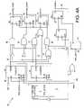
- FIG. 1Ashows control circuitry according to an embodiment of the present invention comprising an oscillator 2 operable to generate an oscillator signal 4 .
- a frequency of the oscillator signal 4increases as an amplitude of a first voltage 6 increases up to a threshold, and the frequency of the oscillator signal 4 decreases as an amplitude of the first voltage 6 exceeds the threshold.
- the oscillator 2is operable to generate a foldover signal 8 indicating when the frequency of the oscillator signal 4 is decreasing due to the first voltage 6 exceeding the threshold.
- the oscillator 2comprises a first ring oscillator operable to generate a first oscillating signal 9 in response to the first voltage 6 , and a second ring oscillator operable to generate a second oscillating signal 10 in response to a second voltage 12 less than the first voltage 6 .
- FIG. 1Bshows an example of how the frequency of the oscillating signals 9 and 10 will increase as the first voltage 6 increases and eventually fold over and start decreasing when the first voltage 6 reaches a threshold.
- the second oscillating signal 10begins decreasing at a higher first voltage 6 since the second voltage 12 is less than the first voltage 6 , therefore the foldover of the oscillator signal 4 can be detected when the frequency of the first oscillating signal 9 falls below the frequency of the second oscillating signal 10 (referred to as the crossover threshold voltage or CTV).
- the embodiment of FIG. 1Acomprises a suitable comparator 20 for comparing the first oscillating signal 9 to the second oscillating signal 10 to generate the foldover signal 8 .
- the second voltage 12is generated by voltage dividing the first voltage 6 so that the first and second voltages vary proportionally.
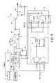
- FIG. 3Bshows an embodiment wherein the switching voltage regulator 22 comprises a frequency generator 34 operable to generate a reference signal 36 representing a target gate speed of the reference circuit.
- a cycle comparator 38compares at least one cycle of the oscillator signal 4 to at least one cycle of the reference signal 36 , and the switching circuitry 26 charges the charging element 30 in response to the comparison.
- any suitable charging elemente.g., an inductor, a capacitor, etc.
- a buck mode voltage regulatoris shown employing an inductor 30 as the charging element.
- the switching voltage regulatormay include a boost mode voltage regulator, or a buck/boost mode voltage regulator.
- the physical location of the elements comprising the switching voltage regulatoris unimportant.
- the oscillator 2may be located on a separate chip from the system circuitry 24 .
- the inductor 30may be located separately from digital circuitry comprising portions of the switching voltage regulator.
- system circuitry 24may comprise any circuitry supplied by a voltage.
- the system circuitry 24may comprise a microprocessor, as would be typically found in a computer.
- the system circuitry 24may comprise analog circuitry configured to perform one or more tasks.
- the oscillator 2is configurable to represent one of a plurality of different circuits (or circuit paths) within the system circuitry 24 depending on a mode of operation (i.e., the reference circuit may be different circuits at different times).
- the oscillator frequencyneed not correspond precisely with the gate speed of the reference circuit, but may instead simply track it (e.g., the oscillator frequency may be a multiple of the corresponding gate speed-equivalent frequency of the reference circuit).
- the oscillator frequencyis directly proportional to the gate speed of the reference circuit. Since the oscillator frequency will vary relative to the magnitude of the supply voltage 6 as well as other factors, such as temperature, adjusting the magnitude of the supply voltage 6 adjusts the frequency of the oscillator signal 4 until the reference circuit is operating at the desired gate speed.
- the simulation and layout software used in the design of the system circuitry 24may provide sophisticated timing analysis of various delays.
- the reference circuit within the system circuitry 24is determined at design time using the simulation and layout software.
- the gates in the oscillator 2 and system circuitry 24may be fabricated together so they have similar characteristics. Some differences may occur due to loading effects and wire routing; however, by adding inverters, lengthening wires through physical placement, adding dummy loads, and placing the oscillator 2 as close as possible to the reference circuit, the oscillator 2 may be configured to substantially match the delay of the reference circuit.
- the oscillator 2will change speed as the temperature changes, as the supply voltage 6 changes, or as the manufacturing process produces faster or slower gates, and thereby track the propagation delay of the reference circuit within the system circuitry 24 .
- an OR gate 56asserts a disable signal 18 through latches 60 and 62 .
- the disable signal 18latches the outputs of latches 48 and 50 through AND gate 64 , and disables the latches 48 and 50 through AND gates 66 and 68 until the next sample period.
- the disable signal 18also disables the oscillator 2 and loads the counters 40 and 44 with appropriate starting values.
- a register 70resets the disable signal 18 when clocked by the reference signal 36 to thereby synchronize the oscillator 2 and the frequency generator 34 .
- the counters 40 and 44 in the embodiment of FIG. 4Aenable scaling of the oscillator frequency or the reference frequency. For example, if the frequency of the oscillator signal 4 should equal half the frequency of the reference signal 36 , then counter 40 is loaded with a starting value that is twice the starting value loaded into counter 44 , from which values the two counters count down at each cycle of the reference and oscillator signals.
- the cycle comparator 38compares multiple cycles of the oscillator signal 4 and reference signal 36 in order to improve the accuracy of the measurement, for example, by compensating for startup transient errors of the ring oscillator 2 .
- counters 40 and 44are loaded with a starting value of 2 in order to compare two cycles of the oscillator signal 4 to two cycles of the reference signal 36 .
- the counters 40 and 44are implemented using simple registers for detecting a single cycle of the reference signal 36 and oscillator signal 4 , respectively.
- the foldover signal 8 generated by the oscillator 2asserts the TIE signal 76 through OR gate 78 before either signal 42 or 46 triggers. As described below with reference to FIG. 5 , asserting the TIE signal 76 prevents the switching circuitry from charging the charging element 30 or adjusting the charge time while the foldover signal 8 is active.
- the comparator 20comprises a first register 80 (e.g., a first counter) clocked by the first oscillating signal 9 , wherein the first register 80 asserts a first signal 82 at the end of the cycle, and a second register 84 (e.g., a second counter) clocked by the second oscillating signal 10 , wherein the second register 84 asserts a second signal 86 at the end of the cycle.
- the comparator 20further comprises a latch 88 for latching the second signal 86 if generated before the first signal 82 and thus outputs the foldover signal 8 indicating when the second oscillating signal 10 is oscillating faster than the first oscillating signal 9 .
- an OR gate 90 and the disable signal 18latch the output of latch 88 through AND gate 92 , and disables the latch 88 through AND gate 94 until the next sample period.
- FIG. 5shows a switching voltage regulator employing an oscillator 2 and cycle comparator 38 according to an embodiment of the present invention.
- a first charging counter 96times a charge time of the charging element 30
- a second charging counter 98times a delay period following the charge time.
- the first and second charging counters 96 and 98are loaded initially with a nominal value generated by a third counter 100 .
- the REF_FAST signal 52When the REF_FAST signal 52 is active (indicating that the output voltage 6 is too low), it enables AND gate 102 and sets register 104 , thereby turning on switch 28 so as to charge the charging element 30 .
- the first charging counter 96When the first charging counter 96 reaches a terminal count, it generates a DONE signal 106 that sets register 108 to disable AND gate 102 and reset register 104 in order to turn off the switch 28 . Register 108 also enables the second charging counter 98 to begin counting.
- the second charging counter 98When the second charging counter 98 reaches a terminal count, it generates a DONE signal 110 that resets register 108 to enable AND gate 102 and thereby enable the next charging cycle.
- the DONE signal 110also enables AND gates 112 and 114 in order to “sample” the REF_FAST signal 52 and OSC_FAST signal 54 to make appropriate adjustments to the charging time. If the REF_FAST signal 52 is high after the delay period established by the second charging counter 98 , it means that the charging time should be increased. Therefore AND gate 112 increments the third counter 100 so as to increment the charge time of the first charging counter 96 and the delay period of the second charging counter 98 .
- the switching voltage regulatorcomprises suitable circuitry to facilitate a startup operation during a power-on restart (POR) event.
- PORpower-on restart
- a POR signal 118enables the charge cycle through OR gate 120 regardless of the discharge level of the current in order to help maintain a sufficient output voltage 6 during the startup operation. Once the switching voltage regulator stabilizes, the POR signal 118 is disabled so that the regulator enters the discontinuous mode.
- a separate oscillator driven by the input voltage 32may generate the oscillator signal for clocking the first and second charging counters 96 and 98 of FIG. 5 . This helps ensure that the charging counters 96 and 98 operate reliably during the startup operation since this separate oscillator is driven by the input voltage rather than by the output voltage 6 .
- the delay period generated by the second charging counter 98may be increased in order to reduce the maximum current flowing through the switch 28 at the beginning of each charge cycle, thereby providing a current limit function to help protect the switch 28 .
- the delay period generated by the second charging counter 98may be increased in any suitable manner, for example, by loading the second charging counter 98 with a larger value, or by adjusting the clock speed of the second charging counter 98 while POR 118 is active.
- FIG. 6shows an embodiment of the present invention wherein the control circuitry comprises a difference circuit 122 for generating an error signal 124 representing a difference between the oscillator signal 4 and a reference signal 36 .
- the difference circuit 122may comprise any suitable circuitry, such as a pair of counters clocked by the oscillator signal 4 and the reference signal 36 respectively, wherein the difference between the counters represents the error signal 124 (frequency error).
- the difference circuit 122may comprise suitable analog circuitry for comparing a phase difference between the oscillator signal 4 and the reference signal 36 .
Landscapes
- Dc-Dc Converters (AREA)
Abstract
Description
Claims (17)
Priority Applications (1)
| Application Number | Priority Date | Filing Date | Title |
|---|---|---|---|
| US11/855,848US7733189B1 (en) | 2007-09-14 | 2007-09-14 | Oscillator comprising foldover detection |
Applications Claiming Priority (1)
| Application Number | Priority Date | Filing Date | Title |
|---|---|---|---|
| US11/855,848US7733189B1 (en) | 2007-09-14 | 2007-09-14 | Oscillator comprising foldover detection |
Publications (1)
| Publication Number | Publication Date |
|---|---|
| US7733189B1true US7733189B1 (en) | 2010-06-08 |
Family
ID=42226907
Family Applications (1)
| Application Number | Title | Priority Date | Filing Date |
|---|---|---|---|
| US11/855,848Active2027-10-17US7733189B1 (en) | 2007-09-14 | 2007-09-14 | Oscillator comprising foldover detection |
Country Status (1)
| Country | Link |
|---|---|
| US (1) | US7733189B1 (en) |
Cited By (117)
| Publication number | Priority date | Publication date | Assignee | Title |
|---|---|---|---|---|
| US20090189702A1 (en)* | 2008-01-28 | 2009-07-30 | Infineon Technologies Ag | Circuit and method for detecting a voltage change |
| US8085020B1 (en)* | 2008-06-13 | 2011-12-27 | Western Digital Technologies, Inc. | Switching voltage regulator employing dynamic voltage scaling with hysteretic comparator |
| US8324974B1 (en) | 2010-12-17 | 2012-12-04 | Western Digital Technologies, Inc. | Regulating power consumption of digital circuitry using a multi-layer ring oscillator |
| US8350628B1 (en) | 2011-02-15 | 2013-01-08 | Western Digital Technologies, Inc. | Gate speed regulator dithering ring oscillator to match critical path circuit |
| US8390367B1 (en) | 2011-02-15 | 2013-03-05 | Western Digital Technologies, Inc. | Ensuring minimum gate speed during startup of gate speed regulator |
| US8395454B2 (en)* | 2011-05-13 | 2013-03-12 | Oracle International Corporation | Synchronized output of multiple ring oscillators |
| US20130127549A1 (en)* | 2011-11-17 | 2013-05-23 | Stmicroelectronics (Rousset) Sas | Clock signal synchronization and disturbance detector |
| US20130187708A1 (en)* | 2012-01-20 | 2013-07-25 | Qualcomm Incorporated | Wide Input Bit-Rate, Power Efficient PWM Decoder |
| US20130208763A1 (en)* | 2012-02-15 | 2013-08-15 | Infineon Technologies Ag | Circuit and method for sensing a physical quantity, an oscillator circuit, a smartcard, and a temperature-sensing circuit |
| US20140022022A1 (en)* | 2012-07-17 | 2014-01-23 | Freescale Semiconductor, Inc. | Error detection at an oscillator |
| US20140197895A1 (en)* | 2013-01-17 | 2014-07-17 | Texas Instruments Incorporated | Variability and aging sensor for integrated circuits |
| US8824081B1 (en) | 2012-03-13 | 2014-09-02 | Western Digital Technologies, Inc. | Disk drive employing radially coherent reference pattern for servo burst demodulation and fly height measurement |
| US8830617B1 (en) | 2013-05-30 | 2014-09-09 | Western Digital Technologies, Inc. | Disk drive adjusting state estimator to compensate for unreliable servo data |
| US8879191B1 (en) | 2012-11-14 | 2014-11-04 | Western Digital Technologies, Inc. | Disk drive modifying rotational position optimization algorithm to achieve target performance for limited stroke |
| US8891191B1 (en) | 2014-05-06 | 2014-11-18 | Western Digital Technologies, Inc. | Data storage device initializing read signal gain to detect servo seed pattern |
| US8891194B1 (en) | 2013-05-14 | 2014-11-18 | Western Digital Technologies, Inc. | Disk drive iteratively adapting correction value that compensates for non-linearity of head |
| US8896957B1 (en) | 2013-05-10 | 2014-11-25 | Western Digital Technologies, Inc. | Disk drive performing spiral scan of disk surface to detect residual data |
| US8902529B1 (en)* | 2012-11-20 | 2014-12-02 | Western Digital Technologies, Inc. | Dual frequency crystal oscillator |
| US8902538B1 (en) | 2013-03-29 | 2014-12-02 | Western Digital Technologies, Inc. | Disk drive detecting crack in microactuator |
| US8902539B1 (en) | 2014-05-13 | 2014-12-02 | Western Digital Technologies, Inc. | Data storage device reducing seek power consumption |
| US8912778B1 (en) | 2006-03-30 | 2014-12-16 | Western Digital Technologies, Inc. | Switching voltage regulator employing current pre-adjust based on power mode |
| US8913342B1 (en) | 2014-03-21 | 2014-12-16 | Western Digital Technologies, Inc. | Data storage device adjusting range of microactuator digital-to-analog converter based on operating temperature |
| US8917474B1 (en) | 2011-08-08 | 2014-12-23 | Western Digital Technologies, Inc. | Disk drive calibrating a velocity profile prior to writing a spiral track |
| US8917475B1 (en) | 2013-12-20 | 2014-12-23 | Western Digital Technologies, Inc. | Disk drive generating a disk locked clock using radial dependent timing feed-forward compensation |
| US8922931B1 (en) | 2013-05-13 | 2014-12-30 | Western Digital Technologies, Inc. | Disk drive releasing variable amount of buffered write data based on sliding window of predicted servo quality |
| US8922938B1 (en) | 2012-11-02 | 2014-12-30 | Western Digital Technologies, Inc. | Disk drive filtering disturbance signal and error signal for adaptive feed-forward compensation |
| US8922940B1 (en) | 2014-05-27 | 2014-12-30 | Western Digital Technologies, Inc. | Data storage device reducing spindle motor voltage boost during power failure |
| US8922937B1 (en) | 2012-04-19 | 2014-12-30 | Western Digital Technologies, Inc. | Disk drive evaluating multiple vibration sensor outputs to enable write-protection |
| US8929022B1 (en) | 2012-12-19 | 2015-01-06 | Western Digital Technologies, Inc. | Disk drive detecting microactuator degradation by evaluating frequency component of servo signal |
| US8929021B1 (en) | 2012-03-27 | 2015-01-06 | Western Digital Technologies, Inc. | Disk drive servo writing from spiral tracks using radial dependent timing feed-forward compensation |
| US8934186B1 (en) | 2014-03-26 | 2015-01-13 | Western Digital Technologies, Inc. | Data storage device estimating servo zone to reduce size of track address |
| US8937784B1 (en) | 2012-08-01 | 2015-01-20 | Western Digital Technologies, Inc. | Disk drive employing feed-forward compensation and phase shift compensation during seek settling |
| US8941945B1 (en) | 2014-06-06 | 2015-01-27 | Western Digital Technologies, Inc. | Data storage device servoing heads based on virtual servo tracks |
| US8941939B1 (en) | 2013-10-24 | 2015-01-27 | Western Digital Technologies, Inc. | Disk drive using VCM BEMF feed-forward compensation to write servo data to a disk |
| US8947819B1 (en) | 2012-08-28 | 2015-02-03 | Western Digital Technologies, Inc. | Disk drive implementing hysteresis for primary shock detector based on a more sensitive secondary shock detector |
| US8953271B1 (en) | 2013-05-13 | 2015-02-10 | Western Digital Technologies, Inc. | Disk drive compensating for repeatable run out selectively per zone |
| US8953278B1 (en) | 2011-11-16 | 2015-02-10 | Western Digital Technologies, Inc. | Disk drive selecting disturbance signal for feed-forward compensation |
| US8958169B1 (en) | 2014-06-11 | 2015-02-17 | Western Digital Technologies, Inc. | Data storage device re-qualifying state estimator while decelerating head |
| US8970979B1 (en) | 2013-12-18 | 2015-03-03 | Western Digital Technologies, Inc. | Disk drive determining frequency response of actuator near servo sample frequency |
| US8982490B1 (en) | 2014-04-24 | 2015-03-17 | Western Digital Technologies, Inc. | Data storage device reading first spiral track while simultaneously writing second spiral track |
| US8982501B1 (en) | 2014-09-22 | 2015-03-17 | Western Digital Technologies, Inc. | Data storage device compensating for repeatable disturbance when commutating a spindle motor |
| US8995082B1 (en) | 2011-06-03 | 2015-03-31 | Western Digital Technologies, Inc. | Reducing acoustic noise in a disk drive when exiting idle mode |
| US8995075B1 (en) | 2012-06-21 | 2015-03-31 | Western Digital Technologies, Inc. | Disk drive adjusting estimated servo state to compensate for transient when crossing a servo zone boundary |
| US9001454B1 (en) | 2013-04-12 | 2015-04-07 | Western Digital Technologies, Inc. | Disk drive adjusting phase of adaptive feed-forward controller when reconfiguring servo loop |
| US9007714B1 (en) | 2014-07-18 | 2015-04-14 | Western Digital Technologies Inc. | Data storage device comprising slew rate anti-windup compensation for microactuator |
| US9013825B1 (en) | 2014-03-24 | 2015-04-21 | Western Digital Technologies, Inc. | Electronic system with vibration management mechanism and method of operation thereof |
| US9013824B1 (en) | 2014-06-04 | 2015-04-21 | Western Digital Technologies, Inc. | Data storage device comprising dual read sensors and dual servo channels to improve servo demodulation |
| US9026728B1 (en) | 2013-06-06 | 2015-05-05 | Western Digital Technologies, Inc. | Disk drive applying feed-forward compensation when writing consecutive data tracks |
| US9025269B1 (en) | 2014-01-02 | 2015-05-05 | Western Digital Technologies, Inc. | Disk drive compensating for cycle slip of disk locked clock when reading mini-wedge |
| US9047932B1 (en) | 2014-03-21 | 2015-06-02 | Western Digital Technologies, Inc. | Data storage device adjusting a power loss threshold based on samples of supply voltage |
| US9047901B1 (en) | 2013-05-28 | 2015-06-02 | Western Digital Technologies, Inc. | Disk drive measuring spiral track error by measuring a slope of a spiral track across a disk radius |
| US9047919B1 (en) | 2013-03-12 | 2015-06-02 | Western Digitial Technologies, Inc. | Disk drive initializing servo read channel by reading data preceding servo preamble during access operation |
| US9053727B1 (en) | 2014-06-02 | 2015-06-09 | Western Digital Technologies, Inc. | Disk drive opening spiral crossing window based on DC and AC spiral track error |
| US9053726B1 (en) | 2014-01-29 | 2015-06-09 | Western Digital Technologies, Inc. | Data storage device on-line adapting disturbance observer filter |
| US9053712B1 (en) | 2014-05-07 | 2015-06-09 | Western Digital Technologies, Inc. | Data storage device reading servo sector while writing data sector |
| US9058827B1 (en) | 2013-06-25 | 2015-06-16 | Western Digitial Technologies, Inc. | Disk drive optimizing filters based on sensor signal and disturbance signal for adaptive feed-forward compensation |
| US9058834B1 (en) | 2013-11-08 | 2015-06-16 | Western Digital Technologies, Inc. | Power architecture for low power modes in storage devices |
| US9058826B1 (en) | 2014-02-13 | 2015-06-16 | Western Digital Technologies, Inc. | Data storage device detecting free fall condition from disk speed variations |
| US9064537B1 (en) | 2013-09-13 | 2015-06-23 | Western Digital Technologies, Inc. | Disk drive measuring radial offset between heads by detecting a difference between ramp contact |
| US9076473B1 (en) | 2014-08-12 | 2015-07-07 | Western Digital Technologies, Inc. | Data storage device detecting fly height instability of head during load operation based on microactuator response |
| US9076471B1 (en) | 2013-07-31 | 2015-07-07 | Western Digital Technologies, Inc. | Fall detection scheme using FFS |
| US9076472B1 (en) | 2014-08-21 | 2015-07-07 | Western Digital (Fremont), Llc | Apparatus enabling writing servo data when disk reaches target rotation speed |
| US9076490B1 (en) | 2012-12-12 | 2015-07-07 | Western Digital Technologies, Inc. | Disk drive writing radial offset spiral servo tracks by reading spiral seed tracks |
| US9093105B2 (en) | 2011-12-09 | 2015-07-28 | Western Digital Technologies, Inc. | Disk drive charging capacitor using motor supply voltage during power failure |
| US9099147B1 (en) | 2014-09-22 | 2015-08-04 | Western Digital Technologies, Inc. | Data storage device commutating a spindle motor using closed-loop rotation phase alignment |
| US9111575B1 (en) | 2014-10-23 | 2015-08-18 | Western Digital Technologies, Inc. | Data storage device employing adaptive feed-forward control in timing loop to compensate for vibration |
| US9129630B1 (en) | 2014-12-16 | 2015-09-08 | Western Digital Technologies, Inc. | Data storage device employing full servo sectors on first disk surface and mini servo sectors on second disk surface |
| US9142249B1 (en) | 2013-12-06 | 2015-09-22 | Western Digital Technologies, Inc. | Disk drive using timing loop control signal for vibration compensation in servo loop |
| US9141177B1 (en) | 2014-03-21 | 2015-09-22 | Western Digital Technologies, Inc. | Data storage device employing glitch compensation for power loss detection |
| US9142235B1 (en) | 2009-10-27 | 2015-09-22 | Western Digital Technologies, Inc. | Disk drive characterizing microactuator by injecting sinusoidal disturbance and evaluating feed-forward compensation values |
| US9142225B1 (en) | 2014-03-21 | 2015-09-22 | Western Digital Technologies, Inc. | Electronic system with actuator control mechanism and method of operation thereof |
| US9147428B1 (en) | 2013-04-24 | 2015-09-29 | Western Digital Technologies, Inc. | Disk drive with improved spin-up control |
| US9147418B1 (en) | 2013-06-20 | 2015-09-29 | Western Digital Technologies, Inc. | Disk drive compensating for microactuator gain variations |
| US9155139B2 (en) | 2012-03-09 | 2015-10-06 | Rockwell Automation Technologies, Inc. | LED driver circuits and methods |
| US9153283B1 (en) | 2014-09-30 | 2015-10-06 | Western Digital Technologies, Inc. | Data storage device compensating for hysteretic response of microactuator |
| US9165583B1 (en) | 2014-10-29 | 2015-10-20 | Western Digital Technologies, Inc. | Data storage device adjusting seek profile based on seek length when ending track is near ramp |
| US9171568B1 (en) | 2014-06-25 | 2015-10-27 | Western Digital Technologies, Inc. | Data storage device periodically re-initializing spindle motor commutation sequence based on timing data |
| US9171567B1 (en) | 2014-05-27 | 2015-10-27 | Western Digital Technologies, Inc. | Data storage device employing sliding mode control of spindle motor |
| US9208808B1 (en) | 2014-04-22 | 2015-12-08 | Western Digital Technologies, Inc. | Electronic system with unload management mechanism and method of operation thereof |
| US9208810B1 (en) | 2014-04-24 | 2015-12-08 | Western Digital Technologies, Inc. | Data storage device attenuating interference from first spiral track when reading second spiral track |
| US9208815B1 (en) | 2014-10-09 | 2015-12-08 | Western Digital Technologies, Inc. | Data storage device dynamically reducing coast velocity during seek to reduce power consumption |
| US9214175B1 (en) | 2015-03-16 | 2015-12-15 | Western Digital Technologies, Inc. | Data storage device configuring a gain of a servo control system for actuating a head over a disk |
| US9230593B1 (en) | 2014-12-23 | 2016-01-05 | Western Digital Technologies, Inc. | Data storage device optimizing spindle motor power when transitioning into a power failure mode |
| US9230592B1 (en) | 2014-12-23 | 2016-01-05 | Western Digital Technologies, Inc. | Electronic system with a method of motor spindle bandwidth estimation and calibration thereof |
| US9245577B1 (en) | 2015-03-26 | 2016-01-26 | Western Digital Technologies, Inc. | Data storage device comprising spindle motor current sensing with supply voltage noise attenuation |
| US9245540B1 (en) | 2014-10-29 | 2016-01-26 | Western Digital Technologies, Inc. | Voice coil motor temperature sensing circuit to reduce catastrophic failure due to voice coil motor coil shorting to ground |
| US9245560B1 (en) | 2015-03-09 | 2016-01-26 | Western Digital Technologies, Inc. | Data storage device measuring reader/writer offset by reading spiral track and concentric servo sectors |
| US9251823B1 (en) | 2014-12-10 | 2016-02-02 | Western Digital Technologies, Inc. | Data storage device delaying seek operation to avoid thermal asperities |
| US9269386B1 (en) | 2014-01-29 | 2016-02-23 | Western Digital Technologies, Inc. | Data storage device on-line adapting disturbance observer filter |
| US9286925B1 (en) | 2015-03-26 | 2016-03-15 | Western Digital Technologies, Inc. | Data storage device writing multiple burst correction values at the same radial location |
| US9286927B1 (en) | 2014-12-16 | 2016-03-15 | Western Digital Technologies, Inc. | Data storage device demodulating servo burst by computing slope of intermediate integration points |
| US9343094B1 (en) | 2015-03-26 | 2016-05-17 | Western Digital Technologies, Inc. | Data storage device filtering burst correction values before downsampling the burst correction values |
| US9343102B1 (en) | 2015-03-25 | 2016-05-17 | Western Digital Technologies, Inc. | Data storage device employing a phase offset to generate power from a spindle motor during a power failure |
| US9350278B1 (en) | 2014-06-13 | 2016-05-24 | Western Digital Technologies, Inc. | Circuit technique to integrate voice coil motor support elements |
| US9349401B1 (en) | 2014-07-24 | 2016-05-24 | Western Digital Technologies, Inc. | Electronic system with media scan mechanism and method of operation thereof |
| US9355676B1 (en) | 2015-03-25 | 2016-05-31 | Western Digital Technologies, Inc. | Data storage device controlling amplitude and phase of driving voltage to generate power from a spindle motor |
| US9355667B1 (en) | 2014-11-11 | 2016-05-31 | Western Digital Technologies, Inc. | Data storage device saving absolute position at each servo wedge for previous write operations |
| US9361939B1 (en) | 2014-03-10 | 2016-06-07 | Western Digital Technologies, Inc. | Data storage device characterizing geometry of magnetic transitions |
| US9396751B1 (en) | 2015-06-26 | 2016-07-19 | Western Digital Technologies, Inc. | Data storage device compensating for fabrication tolerances when measuring spindle motor current |
| US9407015B1 (en) | 2014-12-29 | 2016-08-02 | Western Digital Technologies, Inc. | Automatic power disconnect device |
| US9418689B2 (en) | 2014-10-09 | 2016-08-16 | Western Digital Technologies, Inc. | Data storage device generating an operating seek time profile as a function of a base seek time profile |
| US9424868B1 (en) | 2015-05-12 | 2016-08-23 | Western Digital Technologies, Inc. | Data storage device employing spindle motor driving profile during seek to improve power performance |
| US9424871B1 (en) | 2012-09-13 | 2016-08-23 | Western Digital Technologies, Inc. | Disk drive correcting an error in a detected gray code |
| US9437237B1 (en) | 2015-02-20 | 2016-09-06 | Western Digital Technologies, Inc. | Method to detect power loss through data storage device spindle speed |
| US9437231B1 (en) | 2015-09-25 | 2016-09-06 | Western Digital Technologies, Inc. | Data storage device concurrently controlling and sensing a secondary actuator for actuating a head over a disk |
| US9454212B1 (en) | 2014-12-08 | 2016-09-27 | Western Digital Technologies, Inc. | Wakeup detector |
| US9471072B1 (en) | 2013-11-14 | 2016-10-18 | Western Digital Technologies, Inc | Self-adaptive voltage scaling |
| US9484733B1 (en) | 2013-09-11 | 2016-11-01 | Western Digital Technologies, Inc. | Power control module for data storage device |
| US9542966B1 (en) | 2015-07-09 | 2017-01-10 | Western Digital Technologies, Inc. | Data storage devices and methods with frequency-shaped sliding mode control |
| US9564162B1 (en) | 2015-12-28 | 2017-02-07 | Western Digital Technologies, Inc. | Data storage device measuring resonant frequency of a shock sensor by applying differential excitation and measuring oscillation |
| US9581978B1 (en) | 2014-12-17 | 2017-02-28 | Western Digital Technologies, Inc. | Electronic system with servo management mechanism and method of operation thereof |
| US9620160B1 (en) | 2015-12-28 | 2017-04-11 | Western Digital Technologies, Inc. | Data storage device measuring resonant frequency of a shock sensor by inserting the shock sensor into an oscillator circuit |
| US9823294B1 (en) | 2013-10-29 | 2017-11-21 | Western Digital Technologies, Inc. | Negative voltage testing methodology and tester |
| US9886285B2 (en) | 2015-03-31 | 2018-02-06 | Western Digital Technologies, Inc. | Communication interface initialization |
| US9899834B1 (en) | 2015-11-18 | 2018-02-20 | Western Digital Technologies, Inc. | Power control module using protection circuit for regulating backup voltage to power load during power fault |
| US9959204B1 (en) | 2015-03-09 | 2018-05-01 | Western Digital Technologies, Inc. | Tracking sequential ranges of non-ordered data |
| US11742836B1 (en)* | 2022-04-14 | 2023-08-29 | International Business Machines Corporation | Random number generator using cross-coupled ring oscillators |
Citations (84)
| Publication number | Priority date | Publication date | Assignee | Title |
|---|---|---|---|---|
| US4164648A (en) | 1978-06-23 | 1979-08-14 | Hewlett-Packard Company | Double vernier time interval measurement using triggered phase-locked oscillators |
| US4298898A (en) | 1979-04-19 | 1981-11-03 | Compagnie Internationale Pour L'informatique Cii Honeywell Bull | Method of and apparatus for reading data from reference zones of a memory |
| US4675617A (en) | 1986-02-03 | 1987-06-23 | Martin Kenneth W | Stable voltage controlled oscillator |
| US4737670A (en) | 1984-11-09 | 1988-04-12 | Lsi Logic Corporation | Delay control circuit |
| US4822144A (en) | 1986-12-24 | 1989-04-18 | U.S. Philips Corporation | Electro-optic color display including luminescent layer and interference filter |
| US4922141A (en) | 1986-10-07 | 1990-05-01 | Western Digital Corporation | Phase-locked loop delay line |
| WO1990013079A1 (en) | 1989-04-17 | 1990-11-01 | Motorola, Inc. | Computing system with selective operating voltage |
| US5146121A (en) | 1991-10-24 | 1992-09-08 | Northern Telecom Limited | Signal delay apparatus employing a phase locked loop |
| US5386187A (en) | 1992-09-30 | 1995-01-31 | Siemens Aktiengesellschaft | Method for anticipatory control of a switched-mode power supply for compensating for fluctuations in feed voltage and circuit configuration for performing the method |
| US5440250A (en) | 1993-06-26 | 1995-08-08 | Deutsche Itt Industries Gmbh | Clock-generating circuit for clock-controlled logic circuits |
| US5440520A (en) | 1994-09-16 | 1995-08-08 | Intel Corporation | Integrated circuit device that selects its own supply voltage by controlling a power supply |
| US5446718A (en) | 1992-03-04 | 1995-08-29 | Hitachi, Ltd. | Information recording and reproducing method and system for disc-shaped recording mediums |
| US5459438A (en)* | 1992-12-16 | 1995-10-17 | Mirow; Fred | Negative feedback frequency stabilized pulse oscillator |
| US5479119A (en) | 1994-11-23 | 1995-12-26 | Analog Devices, Inc. | High speed active overvoltage detection and protection for overvoltage sensitive circuits |
| US5612610A (en) | 1993-10-22 | 1997-03-18 | Sgs-Thomson Microelectronics S.R.L | DC-to-DC converter operating in a discontinuous mode |
| US5629610A (en) | 1994-05-06 | 1997-05-13 | Sgs-Thomson Microelectronics S.R.L. | Dual threshold current mode digital PWM controller |
| US5638019A (en) | 1995-11-17 | 1997-06-10 | International Business Machines Corporation | Accurately generating precisely skewed clock signals |
| US5640383A (en) | 1993-11-05 | 1997-06-17 | Sony Corporation | Apparatus and method for reproducing data from a record medium |
| US5661422A (en) | 1995-12-12 | 1997-08-26 | Analog Devices, Inc. | High speed saturation prevention for saturable circuit elements |
| US5717683A (en) | 1992-10-05 | 1998-02-10 | Mitsubishi Denki Kabushiki Kaisha | Optical disk and optical disk drive device |
| US5748050A (en) | 1996-03-29 | 1998-05-05 | Symbios Logic Inc. | Linearization method and apparatus for voltage controlled oscillator |
| US5747976A (en) | 1996-03-26 | 1998-05-05 | Raytheon Company | Constant on-time architecture for switching regulators |
| US5777567A (en) | 1996-06-14 | 1998-07-07 | Sun Microsystems, Inc. | System and method for serial to parallel data conversion using delay line |
| US5787292A (en) | 1996-04-01 | 1998-07-28 | International Business Machines Corporation | Power saving method and apparatus for use in multiple frequency zone drives |
| US5808455A (en) | 1996-11-13 | 1998-09-15 | Micro Linear Corporation | DC-to-DC converter having hysteretic current limiting |
| US5815043A (en)* | 1997-02-13 | 1998-09-29 | Apple Computer, Inc. | Frequency controlled ring oscillator having by passable stages |
| US5994885A (en) | 1993-03-23 | 1999-11-30 | Linear Technology Corporation | Control circuit and method for maintaining high efficiency over broad current ranges in a switching regulator circuit |
| US6031426A (en) | 1998-05-29 | 2000-02-29 | Avant! Corporation | Phase locked loop with digital vernier control |
| US6055287A (en) | 1998-05-26 | 2000-04-25 | Mcewan; Thomas E. | Phase-comparator-less delay locked loop |
| US6125157A (en) | 1997-02-06 | 2000-09-26 | Rambus, Inc. | Delay-locked loop circuitry for clock delay adjustment |
| US6157247A (en) | 1996-08-07 | 2000-12-05 | Motorola, Inc. | Methods and circuits for dynamically adjusting a supply voltage and/or a frequency of a clock signal in a digital circuit |
| US6188206B1 (en) | 1999-12-08 | 2001-02-13 | Intel Corporation | Dynamic hysteresis voltage regulation |
| US6259293B1 (en) | 1999-06-15 | 2001-07-10 | Mitsubishi Denki Kabushiki Kaisha | Delay circuitry, clock generating circuitry, and phase synchronization circuitry |
| US6259327B1 (en) | 1998-12-11 | 2001-07-10 | Cselt - Centro Studi E Laboratori Telecomunicazioni S.P.A. | PLL having circuits for selecting optimum VCO input/output characteristics |
| US6288524B1 (en) | 1999-01-26 | 2001-09-11 | Kabushiki Kaisha Toyoda Jidoshokki Seisakusho | DC/DC converter and a controlling circuit thereof |
| US6333652B1 (en) | 1999-05-27 | 2001-12-25 | Rohm Co. Ltd. | Delay circuit |
| US6356062B1 (en) | 2000-09-27 | 2002-03-12 | Intel Corporation | Degenerative load temperature correction for charge pumps |
| US6396251B2 (en) | 2000-03-07 | 2002-05-28 | Stmicroelectronics S.R.L. | Constant-frequency control circuit for a switching voltage regulator of the hysteretic type |
| US6425086B1 (en) | 1999-04-30 | 2002-07-23 | Intel Corporation | Method and apparatus for dynamic power control of a low power processor |
| US6424184B1 (en) | 1996-09-25 | 2002-07-23 | Matsushita Electric Industrial Co., Ltd. | Frequency-voltage conversion circuit, delay amount judgement circuit, system having frequency-voltage conversion circuit, method of adjusting input/output characteristics of frequency-voltage conversion circuit, and apparatus for automatically adjusting input |
| US6449575B2 (en) | 1999-04-21 | 2002-09-10 | Hewlett-Packard Company | Voltage control of integrated circuits |
| US6449110B1 (en) | 1999-02-03 | 2002-09-10 | Cirrus Logic, Inc. | Optimizing operation of a disk storage system by increasing the gain of a non-linear transducer and correcting the non-linear distortions using a non-linear correction circuit |
| US6515460B1 (en) | 2001-09-10 | 2003-02-04 | National Semiconductor Corporation | Multiphase switching regulator control architecture for low on time systems that enforces current sharing |
| US6525585B1 (en) | 2000-11-21 | 2003-02-25 | Nec Corporation | Fixed-length delay generation circuit |
| US6535735B2 (en) | 2001-03-22 | 2003-03-18 | Skyworks Solutions, Inc. | Critical path adaptive power control |
| US20030093160A1 (en) | 2001-11-09 | 2003-05-15 | The Regents Of The University Of Colorado, A Body Corporate | Adaptive voltage regulator for powered digital devices |
| US6577535B2 (en) | 2001-02-16 | 2003-06-10 | Sandisk Corporation | Method and system for distributed power generation in multi-chip memory systems |
| US6617936B2 (en) | 2001-02-20 | 2003-09-09 | Velio Communications, Inc. | Phase controlled oscillator |
| US6622252B1 (en) | 2000-04-12 | 2003-09-16 | International Business Machines Corporation | Data storage device having selectable performance modes for use in dual powered portable devices |
| US6657467B2 (en) | 2001-08-10 | 2003-12-02 | Sony Corporation | Delay control circuit with internal power supply voltage control |
| US6693473B2 (en) | 2002-03-19 | 2004-02-17 | Infineon Technologies Ag | Delay lock loop having a variable voltage regulator |
| US6721255B1 (en) | 1998-10-28 | 2004-04-13 | Matsushita Electric Industrial Co., Ltd. | Device and method for recording data to optical disk using recording pulse with corrected edge position |
| US6774694B1 (en) | 2001-12-26 | 2004-08-10 | Analog Devices, Inc. | Timing vernier architecture for generating high speed, high accuracy timing edges |
| US6831494B1 (en) | 2003-05-16 | 2004-12-14 | Transmeta Corporation | Voltage compensated integrated circuits |
| US20040257056A1 (en) | 2003-05-09 | 2004-12-23 | Jian-Rong Huang | Switching regulator with improved load transient efficiency and method thereof |
| US6868503B1 (en) | 2002-01-19 | 2005-03-15 | National Semiconductor Corporation | Adaptive voltage scaling digital processing component and method of operating the same |
| US6870410B1 (en) | 2002-10-15 | 2005-03-22 | National Semiconductor Corporation | All digital power supply system and method that provides a substantially constant supply voltage over changes in PVT without a band gap reference voltage |
| US6885210B1 (en) | 2002-04-16 | 2005-04-26 | Transmeta Corporation | System and method for measuring transistor leakage current with a ring oscillator with backbias controls |
| US20050099235A1 (en) | 2003-11-10 | 2005-05-12 | Sharp Kabushiki Kaisha | PLL clock signal generation circuit |
| US6909266B2 (en) | 2002-11-14 | 2005-06-21 | Fyre Storm, Inc. | Method of regulating an output voltage of a power converter by calculating a current value to be applied to an inductor during a time interval immediately following a voltage sensing time interval and varying a duty cycle of a switch during the time interval following the voltage sensing time interval |
| US20050134391A1 (en) | 2003-12-19 | 2005-06-23 | Yasuyuki Kimura | Semiconductor integrated circuit having built-in PLL circuit |
| US20050140418A1 (en) | 2003-12-31 | 2005-06-30 | Ravisangar Muniandy | On-chip frequency degradation compensation |
| US20050218877A1 (en) | 2004-03-31 | 2005-10-06 | Matsushita Electric Industrial Co., Ltd. | Current mode switching regulator with predetermined on time |
| US20050218871A1 (en) | 2003-04-11 | 2005-10-06 | Inyup Kang | Dynamic voltage scaling for portable devices |
| US20050251700A1 (en) | 2004-05-05 | 2005-11-10 | Henderson Eric L | Dynamic voltage scaling system |
| US6970045B1 (en)* | 2003-06-25 | 2005-11-29 | Nel Frequency Controls, Inc. | Redundant clock module |
| US6987380B1 (en) | 2001-11-06 | 2006-01-17 | Linear Technology Corporation | Time-based current control in switching regulators |
| US7042202B2 (en) | 2002-07-10 | 2006-05-09 | Marvell World Trade Ltd | Energy saving discontinuous mode system and method |
| US20060129852A1 (en) | 2004-12-10 | 2006-06-15 | Bonola Thomas J | Bios-based systems and methods of processor power management |
| US20060161678A1 (en) | 2000-06-30 | 2006-07-20 | Emc Corporation | Method and apparatus for implementing high-performance, scaleable data processing and storage systems |
| US7102446B1 (en) | 2005-02-11 | 2006-09-05 | Silicon Image, Inc. | Phase lock loop with coarse control loop having frequency lock detector and device including same |
| US7109695B2 (en) | 2004-12-08 | 2006-09-19 | Kiawe Forest Llc. | Adaptive digital voltage regulator with same-cycle feedback |
| US20060220753A1 (en)* | 2005-03-31 | 2006-10-05 | Boerstler David W | Oscillator array with row and column control |
| US20060227861A1 (en) | 2005-02-22 | 2006-10-12 | Dragan Maksimovic | Digital pulse-width modulator |
| US7129763B1 (en) | 2004-11-08 | 2006-10-31 | Western Digital Technologies, Inc. | Adjusting power consumption of digital circuitry by generating frequency error representing error in propagation delay |
| US7151417B1 (en)* | 2004-06-16 | 2006-12-19 | Transmeta Corporation | System and method for characterizing a potential distribution |
| US7176663B2 (en) | 2002-08-22 | 2007-02-13 | Fujitsu Limited | Control circuit for DC/DC converter |
| US7205805B1 (en)* | 2004-11-02 | 2007-04-17 | Western Digital Technologies, Inc. | Adjusting power consumption of digital circuitry relative to critical path circuit having the largest propagation delay error |
| US7259603B2 (en) | 2004-03-30 | 2007-08-21 | Texas Instruments Incorporated | Switch mode power converter |
| US7276925B2 (en)* | 2005-07-01 | 2007-10-02 | P.A. Semi, Inc. | Operating an integrated circuit at a minimum supply voltage |
| US7330019B1 (en) | 2006-10-31 | 2008-02-12 | Western Digital Technologies, Inc. | Adjusting on-time for a discontinuous switching voltage regulator |
| US7330017B2 (en) | 2004-01-29 | 2008-02-12 | Enpirion, Inc. | Driver for a power converter and a method of driving a switch thereof |
| US7486060B1 (en) | 2006-03-30 | 2009-02-03 | Western Digital Technologies, Inc. | Switching voltage regulator comprising a cycle comparator for dynamic voltage scaling |
| US7551383B1 (en) | 2006-06-28 | 2009-06-23 | Western Digital Technologies, Inc. | Adjusting voltage delivered to disk drive circuitry based on a selected zone |
- 2007
- 2007-09-14USUS11/855,848patent/US7733189B1/enactiveActive
Patent Citations (87)
| Publication number | Priority date | Publication date | Assignee | Title |
|---|---|---|---|---|
| US4164648A (en) | 1978-06-23 | 1979-08-14 | Hewlett-Packard Company | Double vernier time interval measurement using triggered phase-locked oscillators |
| US4298898A (en) | 1979-04-19 | 1981-11-03 | Compagnie Internationale Pour L'informatique Cii Honeywell Bull | Method of and apparatus for reading data from reference zones of a memory |
| US4737670A (en) | 1984-11-09 | 1988-04-12 | Lsi Logic Corporation | Delay control circuit |
| US4675617A (en) | 1986-02-03 | 1987-06-23 | Martin Kenneth W | Stable voltage controlled oscillator |
| US4922141A (en) | 1986-10-07 | 1990-05-01 | Western Digital Corporation | Phase-locked loop delay line |
| US4822144A (en) | 1986-12-24 | 1989-04-18 | U.S. Philips Corporation | Electro-optic color display including luminescent layer and interference filter |
| WO1990013079A1 (en) | 1989-04-17 | 1990-11-01 | Motorola, Inc. | Computing system with selective operating voltage |
| US5146121A (en) | 1991-10-24 | 1992-09-08 | Northern Telecom Limited | Signal delay apparatus employing a phase locked loop |
| US5446718A (en) | 1992-03-04 | 1995-08-29 | Hitachi, Ltd. | Information recording and reproducing method and system for disc-shaped recording mediums |
| US5386187A (en) | 1992-09-30 | 1995-01-31 | Siemens Aktiengesellschaft | Method for anticipatory control of a switched-mode power supply for compensating for fluctuations in feed voltage and circuit configuration for performing the method |
| US5717683A (en) | 1992-10-05 | 1998-02-10 | Mitsubishi Denki Kabushiki Kaisha | Optical disk and optical disk drive device |
| US5459438A (en)* | 1992-12-16 | 1995-10-17 | Mirow; Fred | Negative feedback frequency stabilized pulse oscillator |
| US5994885A (en) | 1993-03-23 | 1999-11-30 | Linear Technology Corporation | Control circuit and method for maintaining high efficiency over broad current ranges in a switching regulator circuit |
| US5440250A (en) | 1993-06-26 | 1995-08-08 | Deutsche Itt Industries Gmbh | Clock-generating circuit for clock-controlled logic circuits |
| US5612610A (en) | 1993-10-22 | 1997-03-18 | Sgs-Thomson Microelectronics S.R.L | DC-to-DC converter operating in a discontinuous mode |
| US5640383A (en) | 1993-11-05 | 1997-06-17 | Sony Corporation | Apparatus and method for reproducing data from a record medium |
| US5629610A (en) | 1994-05-06 | 1997-05-13 | Sgs-Thomson Microelectronics S.R.L. | Dual threshold current mode digital PWM controller |
| US5440520A (en) | 1994-09-16 | 1995-08-08 | Intel Corporation | Integrated circuit device that selects its own supply voltage by controlling a power supply |
| US5479119A (en) | 1994-11-23 | 1995-12-26 | Analog Devices, Inc. | High speed active overvoltage detection and protection for overvoltage sensitive circuits |
| US5638019A (en) | 1995-11-17 | 1997-06-10 | International Business Machines Corporation | Accurately generating precisely skewed clock signals |
| US5661422A (en) | 1995-12-12 | 1997-08-26 | Analog Devices, Inc. | High speed saturation prevention for saturable circuit elements |
| US5747976A (en) | 1996-03-26 | 1998-05-05 | Raytheon Company | Constant on-time architecture for switching regulators |
| US5748050A (en) | 1996-03-29 | 1998-05-05 | Symbios Logic Inc. | Linearization method and apparatus for voltage controlled oscillator |
| US6285263B1 (en) | 1996-03-29 | 2001-09-04 | Lsi Logic Corporation | Linearization method and apparatus for voltage controlled oscillator |
| US5787292A (en) | 1996-04-01 | 1998-07-28 | International Business Machines Corporation | Power saving method and apparatus for use in multiple frequency zone drives |
| US5777567A (en) | 1996-06-14 | 1998-07-07 | Sun Microsystems, Inc. | System and method for serial to parallel data conversion using delay line |
| US6157247A (en) | 1996-08-07 | 2000-12-05 | Motorola, Inc. | Methods and circuits for dynamically adjusting a supply voltage and/or a frequency of a clock signal in a digital circuit |
| US6424184B1 (en) | 1996-09-25 | 2002-07-23 | Matsushita Electric Industrial Co., Ltd. | Frequency-voltage conversion circuit, delay amount judgement circuit, system having frequency-voltage conversion circuit, method of adjusting input/output characteristics of frequency-voltage conversion circuit, and apparatus for automatically adjusting input |
| US5808455A (en) | 1996-11-13 | 1998-09-15 | Micro Linear Corporation | DC-to-DC converter having hysteretic current limiting |
| US6125157A (en) | 1997-02-06 | 2000-09-26 | Rambus, Inc. | Delay-locked loop circuitry for clock delay adjustment |
| US5815043A (en)* | 1997-02-13 | 1998-09-29 | Apple Computer, Inc. | Frequency controlled ring oscillator having by passable stages |
| US6055287A (en) | 1998-05-26 | 2000-04-25 | Mcewan; Thomas E. | Phase-comparator-less delay locked loop |
| US6031426A (en) | 1998-05-29 | 2000-02-29 | Avant! Corporation | Phase locked loop with digital vernier control |
| US6721255B1 (en) | 1998-10-28 | 2004-04-13 | Matsushita Electric Industrial Co., Ltd. | Device and method for recording data to optical disk using recording pulse with corrected edge position |
| US6259327B1 (en) | 1998-12-11 | 2001-07-10 | Cselt - Centro Studi E Laboratori Telecomunicazioni S.P.A. | PLL having circuits for selecting optimum VCO input/output characteristics |
| US6288524B1 (en) | 1999-01-26 | 2001-09-11 | Kabushiki Kaisha Toyoda Jidoshokki Seisakusho | DC/DC converter and a controlling circuit thereof |
| US6449110B1 (en) | 1999-02-03 | 2002-09-10 | Cirrus Logic, Inc. | Optimizing operation of a disk storage system by increasing the gain of a non-linear transducer and correcting the non-linear distortions using a non-linear correction circuit |
| US6449575B2 (en) | 1999-04-21 | 2002-09-10 | Hewlett-Packard Company | Voltage control of integrated circuits |
| US6425086B1 (en) | 1999-04-30 | 2002-07-23 | Intel Corporation | Method and apparatus for dynamic power control of a low power processor |
| US6333652B1 (en) | 1999-05-27 | 2001-12-25 | Rohm Co. Ltd. | Delay circuit |
| US6259293B1 (en) | 1999-06-15 | 2001-07-10 | Mitsubishi Denki Kabushiki Kaisha | Delay circuitry, clock generating circuitry, and phase synchronization circuitry |
| US6188206B1 (en) | 1999-12-08 | 2001-02-13 | Intel Corporation | Dynamic hysteresis voltage regulation |
| US6396251B2 (en) | 2000-03-07 | 2002-05-28 | Stmicroelectronics S.R.L. | Constant-frequency control circuit for a switching voltage regulator of the hysteretic type |
| US6622252B1 (en) | 2000-04-12 | 2003-09-16 | International Business Machines Corporation | Data storage device having selectable performance modes for use in dual powered portable devices |
| US20060161678A1 (en) | 2000-06-30 | 2006-07-20 | Emc Corporation | Method and apparatus for implementing high-performance, scaleable data processing and storage systems |
| US6356062B1 (en) | 2000-09-27 | 2002-03-12 | Intel Corporation | Degenerative load temperature correction for charge pumps |
| US6525585B1 (en) | 2000-11-21 | 2003-02-25 | Nec Corporation | Fixed-length delay generation circuit |
| US6577535B2 (en) | 2001-02-16 | 2003-06-10 | Sandisk Corporation | Method and system for distributed power generation in multi-chip memory systems |
| US6617936B2 (en) | 2001-02-20 | 2003-09-09 | Velio Communications, Inc. | Phase controlled oscillator |
| US6535735B2 (en) | 2001-03-22 | 2003-03-18 | Skyworks Solutions, Inc. | Critical path adaptive power control |
| US6657467B2 (en) | 2001-08-10 | 2003-12-02 | Sony Corporation | Delay control circuit with internal power supply voltage control |
| US6515460B1 (en) | 2001-09-10 | 2003-02-04 | National Semiconductor Corporation | Multiphase switching regulator control architecture for low on time systems that enforces current sharing |
| US6987380B1 (en) | 2001-11-06 | 2006-01-17 | Linear Technology Corporation | Time-based current control in switching regulators |
| US20030093160A1 (en) | 2001-11-09 | 2003-05-15 | The Regents Of The University Of Colorado, A Body Corporate | Adaptive voltage regulator for powered digital devices |
| US7061292B2 (en) | 2001-11-09 | 2006-06-13 | The Regents Of The University Of Colorado | Adaptive voltage regulator for powered digital devices |
| US6774694B1 (en) | 2001-12-26 | 2004-08-10 | Analog Devices, Inc. | Timing vernier architecture for generating high speed, high accuracy timing edges |
| US6868503B1 (en) | 2002-01-19 | 2005-03-15 | National Semiconductor Corporation | Adaptive voltage scaling digital processing component and method of operating the same |
| US6693473B2 (en) | 2002-03-19 | 2004-02-17 | Infineon Technologies Ag | Delay lock loop having a variable voltage regulator |
| US6885210B1 (en) | 2002-04-16 | 2005-04-26 | Transmeta Corporation | System and method for measuring transistor leakage current with a ring oscillator with backbias controls |
| US7042202B2 (en) | 2002-07-10 | 2006-05-09 | Marvell World Trade Ltd | Energy saving discontinuous mode system and method |
| US7176663B2 (en) | 2002-08-22 | 2007-02-13 | Fujitsu Limited | Control circuit for DC/DC converter |
| US6870410B1 (en) | 2002-10-15 | 2005-03-22 | National Semiconductor Corporation | All digital power supply system and method that provides a substantially constant supply voltage over changes in PVT without a band gap reference voltage |
| US6909266B2 (en) | 2002-11-14 | 2005-06-21 | Fyre Storm, Inc. | Method of regulating an output voltage of a power converter by calculating a current value to be applied to an inductor during a time interval immediately following a voltage sensing time interval and varying a duty cycle of a switch during the time interval following the voltage sensing time interval |
| US20050218871A1 (en) | 2003-04-11 | 2005-10-06 | Inyup Kang | Dynamic voltage scaling for portable devices |
| US20040257056A1 (en) | 2003-05-09 | 2004-12-23 | Jian-Rong Huang | Switching regulator with improved load transient efficiency and method thereof |
| US6831494B1 (en) | 2003-05-16 | 2004-12-14 | Transmeta Corporation | Voltage compensated integrated circuits |
| US6970045B1 (en)* | 2003-06-25 | 2005-11-29 | Nel Frequency Controls, Inc. | Redundant clock module |
| US20050099235A1 (en) | 2003-11-10 | 2005-05-12 | Sharp Kabushiki Kaisha | PLL clock signal generation circuit |
| US20050134391A1 (en) | 2003-12-19 | 2005-06-23 | Yasuyuki Kimura | Semiconductor integrated circuit having built-in PLL circuit |
| US7015735B2 (en) | 2003-12-19 | 2006-03-21 | Renesas Technology Corp. | Semiconductor integrated circuit having built-in PLL circuit |
| US20050140418A1 (en) | 2003-12-31 | 2005-06-30 | Ravisangar Muniandy | On-chip frequency degradation compensation |
| US7330017B2 (en) | 2004-01-29 | 2008-02-12 | Enpirion, Inc. | Driver for a power converter and a method of driving a switch thereof |
| US7259603B2 (en) | 2004-03-30 | 2007-08-21 | Texas Instruments Incorporated | Switch mode power converter |
| US20050218877A1 (en) | 2004-03-31 | 2005-10-06 | Matsushita Electric Industrial Co., Ltd. | Current mode switching regulator with predetermined on time |
| US20050251700A1 (en) | 2004-05-05 | 2005-11-10 | Henderson Eric L | Dynamic voltage scaling system |
| US7151417B1 (en)* | 2004-06-16 | 2006-12-19 | Transmeta Corporation | System and method for characterizing a potential distribution |
| US7205805B1 (en)* | 2004-11-02 | 2007-04-17 | Western Digital Technologies, Inc. | Adjusting power consumption of digital circuitry relative to critical path circuit having the largest propagation delay error |
| US7129763B1 (en) | 2004-11-08 | 2006-10-31 | Western Digital Technologies, Inc. | Adjusting power consumption of digital circuitry by generating frequency error representing error in propagation delay |
| US7109695B2 (en) | 2004-12-08 | 2006-09-19 | Kiawe Forest Llc. | Adaptive digital voltage regulator with same-cycle feedback |
| US20060129852A1 (en) | 2004-12-10 | 2006-06-15 | Bonola Thomas J | Bios-based systems and methods of processor power management |
| US7102446B1 (en) | 2005-02-11 | 2006-09-05 | Silicon Image, Inc. | Phase lock loop with coarse control loop having frequency lock detector and device including same |
| US20060227861A1 (en) | 2005-02-22 | 2006-10-12 | Dragan Maksimovic | Digital pulse-width modulator |
| US20060220753A1 (en)* | 2005-03-31 | 2006-10-05 | Boerstler David W | Oscillator array with row and column control |
| US7276925B2 (en)* | 2005-07-01 | 2007-10-02 | P.A. Semi, Inc. | Operating an integrated circuit at a minimum supply voltage |
| US7486060B1 (en) | 2006-03-30 | 2009-02-03 | Western Digital Technologies, Inc. | Switching voltage regulator comprising a cycle comparator for dynamic voltage scaling |
| US7551383B1 (en) | 2006-06-28 | 2009-06-23 | Western Digital Technologies, Inc. | Adjusting voltage delivered to disk drive circuitry based on a selected zone |
| US7330019B1 (en) | 2006-10-31 | 2008-02-12 | Western Digital Technologies, Inc. | Adjusting on-time for a discontinuous switching voltage regulator |
Non-Patent Citations (18)
| Title |
|---|
| "Applications for White LED Driver in Parallel vs. Series," Analog Integrations Corporation (AIC), AIC1845, AN027, www.analog.com, pp. 1-7, Oct. 2003. |
| "Power Supply Regulation," printout from Altera website, http://www.altera.com/support/devices/power/regulators/powregulators.html, pp. 1-3, Oct. 2006. |
| Aleksandar Prodic, et al., "Mixed-Signal Simulation of Digitally Controlled Switching Converters," IEEE COMPEL, pp. 100-105, Jun. 2002. |
| Alexander Klaiber, "The Technology Behind Crusoe Processors, Low-Power x86-Compatible Processors Implemented with Code Morphing Software," Transmeta Corporation, pp. 1-18, Jan. 2000. |
| Anthony John Stratakos, "High-Efficiency Low-Voltage DC-DC Conversion for Portable Applications," pp. 1, 124-129, 177-183, 188-191, Ph.D. Dissertation, University of California, Berkley, Dec. 1998. |
| Application as filed-U.S. Appl. No. 11/393,425, filed Mar. 30, 2006, 18 pages. |
| Application as filed-U.S. Appl. No. 11/590,704, filed Oct. 31, 2006, 24 pages. |
| Boit, et al., Interaction of Laser Beam with Semiconductor Device (IC), Retrieved Jan. 29, 2009 from http://mikro.ee.tu-berlin.de/hIb/emmi/poster-emmi1.pdf.* |
| Gu-Yeon Wei et al., "A Fully Digital, Energy-Efficient, Adaptive Power-Supply Regulator", IEEE Journal of Solid-State Circuits, vol. 34, No. 4, pp. 520-528, Apr. 1999. |
| Jinwen Xiao, et al., "A 4-muA Quiescent-Current Dual-Mode Digitally Controlled Buck Converter IC for Cellular Phone Applications," IEEE Journal of Solid-State Circuits, vol. 39, No. 12, pp. 2342-2348, Dec. 2004. |
| Jinwen Xiao, et al., "A 4-μA Quiescent-Current Dual-Mode Digitally Controlled Buck Converter IC for Cellular Phone Applications," IEEE Journal of Solid-State Circuits, vol. 39, No. 12, pp. 2342-2348, Dec. 2004. |
| Lu Yun, et al., "A Current Steering Logic Based Ring Oscillator for High Stability and Lower Noise Applications", High Density packaging and Microsystem Integration, 2007. HDP '07. International Symposium on, Jun. 26-28, 2007, pp. 1-3.* |
| Marc Fleischmann, "LongRun Power Management, Dynamic Power Management for Crusoe Processors," Transmeta Corporation, pp. 1-18, Jan. 17, 2001. |
| Moore, B., et al., "Design of wireless sub-micron characterization system", VLSI Test Symposium, 2004. Proceedings. 22nd IEEE, Apr. 25-29, 2004, pp. 341-346.* |
| Shamim Choudhury, "Designing a TMS320F280x Based Digitally Controlled DC-DC Switching Power Supply," Texas Instruments Application Report, http://focus.ti.com, spraab3.pdf, pp. 1-16, Jul. 2005. |
| T. D. Burd, et al., "A Dynamic Voltage Scaled Microprocessor System," IEEE Journal of Solid-State Circuits, vol. 35, No. 11, pp. 1571-1580, Nov. 2000. |
| Wang et al., "Technology Challenges Motivating Adaptive Techniques", Adaptive Techniques for Dynamic Processor Optimization, Spring US, ISSN 1558-9412, 2008, pp. 1-23.* |
| Wei, Gu-Yeon, "Energy-Efficient I/O Interface Design With Adaptive Power-Supply Regulation",A Dissertation Submitted to the Department of Electrical Engineering and the Committee on Graduate Studies of Stanford University, Jun. 2001, retrieved from http://www-vlsi.stanford.edu/papers/gyw-thesis.pdf on Jan. 29, 2009.* |
Cited By (128)
| Publication number | Priority date | Publication date | Assignee | Title |
|---|---|---|---|---|
| US8912778B1 (en) | 2006-03-30 | 2014-12-16 | Western Digital Technologies, Inc. | Switching voltage regulator employing current pre-adjust based on power mode |
| US7859421B2 (en)* | 2008-01-28 | 2010-12-28 | Infineon Technologies Ag | Circuit and method for detecting a voltage change |
| US20090189702A1 (en)* | 2008-01-28 | 2009-07-30 | Infineon Technologies Ag | Circuit and method for detecting a voltage change |
| US8085020B1 (en)* | 2008-06-13 | 2011-12-27 | Western Digital Technologies, Inc. | Switching voltage regulator employing dynamic voltage scaling with hysteretic comparator |
| US9142235B1 (en) | 2009-10-27 | 2015-09-22 | Western Digital Technologies, Inc. | Disk drive characterizing microactuator by injecting sinusoidal disturbance and evaluating feed-forward compensation values |
| US8324974B1 (en) | 2010-12-17 | 2012-12-04 | Western Digital Technologies, Inc. | Regulating power consumption of digital circuitry using a multi-layer ring oscillator |
| US8350628B1 (en) | 2011-02-15 | 2013-01-08 | Western Digital Technologies, Inc. | Gate speed regulator dithering ring oscillator to match critical path circuit |
| US8390367B1 (en) | 2011-02-15 | 2013-03-05 | Western Digital Technologies, Inc. | Ensuring minimum gate speed during startup of gate speed regulator |
| US8395454B2 (en)* | 2011-05-13 | 2013-03-12 | Oracle International Corporation | Synchronized output of multiple ring oscillators |
| US8995082B1 (en) | 2011-06-03 | 2015-03-31 | Western Digital Technologies, Inc. | Reducing acoustic noise in a disk drive when exiting idle mode |
| US8917474B1 (en) | 2011-08-08 | 2014-12-23 | Western Digital Technologies, Inc. | Disk drive calibrating a velocity profile prior to writing a spiral track |
| US8953278B1 (en) | 2011-11-16 | 2015-02-10 | Western Digital Technologies, Inc. | Disk drive selecting disturbance signal for feed-forward compensation |
| US9251379B2 (en)* | 2011-11-17 | 2016-02-02 | Stmicroelectronics Rousset Sas | Clock signal synchronization and disturbance detector |
| US20130127549A1 (en)* | 2011-11-17 | 2013-05-23 | Stmicroelectronics (Rousset) Sas | Clock signal synchronization and disturbance detector |
| US9390749B2 (en) | 2011-12-09 | 2016-07-12 | Western Digital Technologies, Inc. | Power failure management in disk drives |
| US9093105B2 (en) | 2011-12-09 | 2015-07-28 | Western Digital Technologies, Inc. | Disk drive charging capacitor using motor supply voltage during power failure |
| US8564365B2 (en)* | 2012-01-20 | 2013-10-22 | Qualcomm Incorporated | Wide input bit-rate, power efficient PWM decoder |
| US20130187708A1 (en)* | 2012-01-20 | 2013-07-25 | Qualcomm Incorporated | Wide Input Bit-Rate, Power Efficient PWM Decoder |
| US8979362B2 (en)* | 2012-02-15 | 2015-03-17 | Infineon Technologies Ag | Circuit and method for sensing a physical quantity, an oscillator circuit, a smartcard, and a temperature-sensing circuit |
| US20130208763A1 (en)* | 2012-02-15 | 2013-08-15 | Infineon Technologies Ag | Circuit and method for sensing a physical quantity, an oscillator circuit, a smartcard, and a temperature-sensing circuit |
| US9155139B2 (en) | 2012-03-09 | 2015-10-06 | Rockwell Automation Technologies, Inc. | LED driver circuits and methods |
| US8824081B1 (en) | 2012-03-13 | 2014-09-02 | Western Digital Technologies, Inc. | Disk drive employing radially coherent reference pattern for servo burst demodulation and fly height measurement |
| US8934191B1 (en) | 2012-03-27 | 2015-01-13 | Western Digital Technologies, Inc. | Disk drive generating a disk locked clock using radial dependent timing feed-forward compensation |
| US8929021B1 (en) | 2012-03-27 | 2015-01-06 | Western Digital Technologies, Inc. | Disk drive servo writing from spiral tracks using radial dependent timing feed-forward compensation |
| US8922937B1 (en) | 2012-04-19 | 2014-12-30 | Western Digital Technologies, Inc. | Disk drive evaluating multiple vibration sensor outputs to enable write-protection |
| US9454989B1 (en) | 2012-06-21 | 2016-09-27 | Western Digital Technologies, Inc. | Disk drive adjusting estimated servo state to compensate for transient when crossing a servo zone boundary |
| US8995075B1 (en) | 2012-06-21 | 2015-03-31 | Western Digital Technologies, Inc. | Disk drive adjusting estimated servo state to compensate for transient when crossing a servo zone boundary |
| US8786374B2 (en)* | 2012-07-17 | 2014-07-22 | Freescale Semiconductor, Inc. | Error detection at an oscillator |
| US20140022022A1 (en)* | 2012-07-17 | 2014-01-23 | Freescale Semiconductor, Inc. | Error detection at an oscillator |
| US8937784B1 (en) | 2012-08-01 | 2015-01-20 | Western Digital Technologies, Inc. | Disk drive employing feed-forward compensation and phase shift compensation during seek settling |
| US8947819B1 (en) | 2012-08-28 | 2015-02-03 | Western Digital Technologies, Inc. | Disk drive implementing hysteresis for primary shock detector based on a more sensitive secondary shock detector |
| US9424871B1 (en) | 2012-09-13 | 2016-08-23 | Western Digital Technologies, Inc. | Disk drive correcting an error in a detected gray code |
| US8922938B1 (en) | 2012-11-02 | 2014-12-30 | Western Digital Technologies, Inc. | Disk drive filtering disturbance signal and error signal for adaptive feed-forward compensation |
| US8879191B1 (en) | 2012-11-14 | 2014-11-04 | Western Digital Technologies, Inc. | Disk drive modifying rotational position optimization algorithm to achieve target performance for limited stroke |
| US8902529B1 (en)* | 2012-11-20 | 2014-12-02 | Western Digital Technologies, Inc. | Dual frequency crystal oscillator |
| US9076490B1 (en) | 2012-12-12 | 2015-07-07 | Western Digital Technologies, Inc. | Disk drive writing radial offset spiral servo tracks by reading spiral seed tracks |
| US8929022B1 (en) | 2012-12-19 | 2015-01-06 | Western Digital Technologies, Inc. | Disk drive detecting microactuator degradation by evaluating frequency component of servo signal |
| US9035706B2 (en)* | 2013-01-17 | 2015-05-19 | Texas Instruments Incorporated | Variability and aging sensor for integrated circuits |
| US20140197895A1 (en)* | 2013-01-17 | 2014-07-17 | Texas Instruments Incorporated | Variability and aging sensor for integrated circuits |
| US9047919B1 (en) | 2013-03-12 | 2015-06-02 | Western Digitial Technologies, Inc. | Disk drive initializing servo read channel by reading data preceding servo preamble during access operation |
| US8902538B1 (en) | 2013-03-29 | 2014-12-02 | Western Digital Technologies, Inc. | Disk drive detecting crack in microactuator |
| US9001454B1 (en) | 2013-04-12 | 2015-04-07 | Western Digital Technologies, Inc. | Disk drive adjusting phase of adaptive feed-forward controller when reconfiguring servo loop |
| US9147428B1 (en) | 2013-04-24 | 2015-09-29 | Western Digital Technologies, Inc. | Disk drive with improved spin-up control |
| US8896957B1 (en) | 2013-05-10 | 2014-11-25 | Western Digital Technologies, Inc. | Disk drive performing spiral scan of disk surface to detect residual data |
| US8953271B1 (en) | 2013-05-13 | 2015-02-10 | Western Digital Technologies, Inc. | Disk drive compensating for repeatable run out selectively per zone |
| US8922931B1 (en) | 2013-05-13 | 2014-12-30 | Western Digital Technologies, Inc. | Disk drive releasing variable amount of buffered write data based on sliding window of predicted servo quality |
| US8891194B1 (en) | 2013-05-14 | 2014-11-18 | Western Digital Technologies, Inc. | Disk drive iteratively adapting correction value that compensates for non-linearity of head |
| US9047901B1 (en) | 2013-05-28 | 2015-06-02 | Western Digital Technologies, Inc. | Disk drive measuring spiral track error by measuring a slope of a spiral track across a disk radius |
| US8830617B1 (en) | 2013-05-30 | 2014-09-09 | Western Digital Technologies, Inc. | Disk drive adjusting state estimator to compensate for unreliable servo data |
| US9026728B1 (en) | 2013-06-06 | 2015-05-05 | Western Digital Technologies, Inc. | Disk drive applying feed-forward compensation when writing consecutive data tracks |
| US9147418B1 (en) | 2013-06-20 | 2015-09-29 | Western Digital Technologies, Inc. | Disk drive compensating for microactuator gain variations |
| US9058827B1 (en) | 2013-06-25 | 2015-06-16 | Western Digitial Technologies, Inc. | Disk drive optimizing filters based on sensor signal and disturbance signal for adaptive feed-forward compensation |
| US9076471B1 (en) | 2013-07-31 | 2015-07-07 | Western Digital Technologies, Inc. | Fall detection scheme using FFS |
| US9484733B1 (en) | 2013-09-11 | 2016-11-01 | Western Digital Technologies, Inc. | Power control module for data storage device |
| US9064537B1 (en) | 2013-09-13 | 2015-06-23 | Western Digital Technologies, Inc. | Disk drive measuring radial offset between heads by detecting a difference between ramp contact |
| US8941939B1 (en) | 2013-10-24 | 2015-01-27 | Western Digital Technologies, Inc. | Disk drive using VCM BEMF feed-forward compensation to write servo data to a disk |
| US9823294B1 (en) | 2013-10-29 | 2017-11-21 | Western Digital Technologies, Inc. | Negative voltage testing methodology and tester |
| US9058834B1 (en) | 2013-11-08 | 2015-06-16 | Western Digital Technologies, Inc. | Power architecture for low power modes in storage devices |
| US9471072B1 (en) | 2013-11-14 | 2016-10-18 | Western Digital Technologies, Inc | Self-adaptive voltage scaling |
| US9142249B1 (en) | 2013-12-06 | 2015-09-22 | Western Digital Technologies, Inc. | Disk drive using timing loop control signal for vibration compensation in servo loop |
| US8970979B1 (en) | 2013-12-18 | 2015-03-03 | Western Digital Technologies, Inc. | Disk drive determining frequency response of actuator near servo sample frequency |
| US8917475B1 (en) | 2013-12-20 | 2014-12-23 | Western Digital Technologies, Inc. | Disk drive generating a disk locked clock using radial dependent timing feed-forward compensation |
| US9025269B1 (en) | 2014-01-02 | 2015-05-05 | Western Digital Technologies, Inc. | Disk drive compensating for cycle slip of disk locked clock when reading mini-wedge |
| US9269386B1 (en) | 2014-01-29 | 2016-02-23 | Western Digital Technologies, Inc. | Data storage device on-line adapting disturbance observer filter |
| US9053726B1 (en) | 2014-01-29 | 2015-06-09 | Western Digital Technologies, Inc. | Data storage device on-line adapting disturbance observer filter |
| US9058826B1 (en) | 2014-02-13 | 2015-06-16 | Western Digital Technologies, Inc. | Data storage device detecting free fall condition from disk speed variations |
| US9361939B1 (en) | 2014-03-10 | 2016-06-07 | Western Digital Technologies, Inc. | Data storage device characterizing geometry of magnetic transitions |
| US9141177B1 (en) | 2014-03-21 | 2015-09-22 | Western Digital Technologies, Inc. | Data storage device employing glitch compensation for power loss detection |
| US8913342B1 (en) | 2014-03-21 | 2014-12-16 | Western Digital Technologies, Inc. | Data storage device adjusting range of microactuator digital-to-analog converter based on operating temperature |
| US9142225B1 (en) | 2014-03-21 | 2015-09-22 | Western Digital Technologies, Inc. | Electronic system with actuator control mechanism and method of operation thereof |
| US9047932B1 (en) | 2014-03-21 | 2015-06-02 | Western Digital Technologies, Inc. | Data storage device adjusting a power loss threshold based on samples of supply voltage |
| US9013825B1 (en) | 2014-03-24 | 2015-04-21 | Western Digital Technologies, Inc. | Electronic system with vibration management mechanism and method of operation thereof |
| US8934186B1 (en) | 2014-03-26 | 2015-01-13 | Western Digital Technologies, Inc. | Data storage device estimating servo zone to reduce size of track address |
| US9208808B1 (en) | 2014-04-22 | 2015-12-08 | Western Digital Technologies, Inc. | Electronic system with unload management mechanism and method of operation thereof |
| US8982490B1 (en) | 2014-04-24 | 2015-03-17 | Western Digital Technologies, Inc. | Data storage device reading first spiral track while simultaneously writing second spiral track |
| US9208810B1 (en) | 2014-04-24 | 2015-12-08 | Western Digital Technologies, Inc. | Data storage device attenuating interference from first spiral track when reading second spiral track |
| US8891191B1 (en) | 2014-05-06 | 2014-11-18 | Western Digital Technologies, Inc. | Data storage device initializing read signal gain to detect servo seed pattern |
| US9053712B1 (en) | 2014-05-07 | 2015-06-09 | Western Digital Technologies, Inc. | Data storage device reading servo sector while writing data sector |
| US8902539B1 (en) | 2014-05-13 | 2014-12-02 | Western Digital Technologies, Inc. | Data storage device reducing seek power consumption |
| US8922940B1 (en) | 2014-05-27 | 2014-12-30 | Western Digital Technologies, Inc. | Data storage device reducing spindle motor voltage boost during power failure |
| US9171567B1 (en) | 2014-05-27 | 2015-10-27 | Western Digital Technologies, Inc. | Data storage device employing sliding mode control of spindle motor |
| US9053727B1 (en) | 2014-06-02 | 2015-06-09 | Western Digital Technologies, Inc. | Disk drive opening spiral crossing window based on DC and AC spiral track error |
| US9013824B1 (en) | 2014-06-04 | 2015-04-21 | Western Digital Technologies, Inc. | Data storage device comprising dual read sensors and dual servo channels to improve servo demodulation |
| US8941945B1 (en) | 2014-06-06 | 2015-01-27 | Western Digital Technologies, Inc. | Data storage device servoing heads based on virtual servo tracks |
| US8958169B1 (en) | 2014-06-11 | 2015-02-17 | Western Digital Technologies, Inc. | Data storage device re-qualifying state estimator while decelerating head |
| US9350278B1 (en) | 2014-06-13 | 2016-05-24 | Western Digital Technologies, Inc. | Circuit technique to integrate voice coil motor support elements |
| US9171568B1 (en) | 2014-06-25 | 2015-10-27 | Western Digital Technologies, Inc. | Data storage device periodically re-initializing spindle motor commutation sequence based on timing data |
| US9007714B1 (en) | 2014-07-18 | 2015-04-14 | Western Digital Technologies Inc. | Data storage device comprising slew rate anti-windup compensation for microactuator |
| US9349401B1 (en) | 2014-07-24 | 2016-05-24 | Western Digital Technologies, Inc. | Electronic system with media scan mechanism and method of operation thereof |
| US9076473B1 (en) | 2014-08-12 | 2015-07-07 | Western Digital Technologies, Inc. | Data storage device detecting fly height instability of head during load operation based on microactuator response |
| US9076472B1 (en) | 2014-08-21 | 2015-07-07 | Western Digital (Fremont), Llc | Apparatus enabling writing servo data when disk reaches target rotation speed |
| US9099147B1 (en) | 2014-09-22 | 2015-08-04 | Western Digital Technologies, Inc. | Data storage device commutating a spindle motor using closed-loop rotation phase alignment |
| US8982501B1 (en) | 2014-09-22 | 2015-03-17 | Western Digital Technologies, Inc. | Data storage device compensating for repeatable disturbance when commutating a spindle motor |
| US9153283B1 (en) | 2014-09-30 | 2015-10-06 | Western Digital Technologies, Inc. | Data storage device compensating for hysteretic response of microactuator |
| US9208815B1 (en) | 2014-10-09 | 2015-12-08 | Western Digital Technologies, Inc. | Data storage device dynamically reducing coast velocity during seek to reduce power consumption |
| US9418689B2 (en) | 2014-10-09 | 2016-08-16 | Western Digital Technologies, Inc. | Data storage device generating an operating seek time profile as a function of a base seek time profile |
| US9111575B1 (en) | 2014-10-23 | 2015-08-18 | Western Digital Technologies, Inc. | Data storage device employing adaptive feed-forward control in timing loop to compensate for vibration |
| US9165583B1 (en) | 2014-10-29 | 2015-10-20 | Western Digital Technologies, Inc. | Data storage device adjusting seek profile based on seek length when ending track is near ramp |
| US9245540B1 (en) | 2014-10-29 | 2016-01-26 | Western Digital Technologies, Inc. | Voice coil motor temperature sensing circuit to reduce catastrophic failure due to voice coil motor coil shorting to ground |
| US9355667B1 (en) | 2014-11-11 | 2016-05-31 | Western Digital Technologies, Inc. | Data storage device saving absolute position at each servo wedge for previous write operations |
| US9454212B1 (en) | 2014-12-08 | 2016-09-27 | Western Digital Technologies, Inc. | Wakeup detector |
| US9251823B1 (en) | 2014-12-10 | 2016-02-02 | Western Digital Technologies, Inc. | Data storage device delaying seek operation to avoid thermal asperities |
| US9286927B1 (en) | 2014-12-16 | 2016-03-15 | Western Digital Technologies, Inc. | Data storage device demodulating servo burst by computing slope of intermediate integration points |
| US9129630B1 (en) | 2014-12-16 | 2015-09-08 | Western Digital Technologies, Inc. | Data storage device employing full servo sectors on first disk surface and mini servo sectors on second disk surface |
| US9581978B1 (en) | 2014-12-17 | 2017-02-28 | Western Digital Technologies, Inc. | Electronic system with servo management mechanism and method of operation thereof |
| US9761266B2 (en) | 2014-12-23 | 2017-09-12 | Western Digital Technologies, Inc. | Data storage device optimizing spindle motor power when transitioning into a power failure mode |
| US9230593B1 (en) | 2014-12-23 | 2016-01-05 | Western Digital Technologies, Inc. | Data storage device optimizing spindle motor power when transitioning into a power failure mode |
| US9230592B1 (en) | 2014-12-23 | 2016-01-05 | Western Digital Technologies, Inc. | Electronic system with a method of motor spindle bandwidth estimation and calibration thereof |
| US9407015B1 (en) | 2014-12-29 | 2016-08-02 | Western Digital Technologies, Inc. | Automatic power disconnect device |
| US9437237B1 (en) | 2015-02-20 | 2016-09-06 | Western Digital Technologies, Inc. | Method to detect power loss through data storage device spindle speed |
| US9959204B1 (en) | 2015-03-09 | 2018-05-01 | Western Digital Technologies, Inc. | Tracking sequential ranges of non-ordered data |
| US9245560B1 (en) | 2015-03-09 | 2016-01-26 | Western Digital Technologies, Inc. | Data storage device measuring reader/writer offset by reading spiral track and concentric servo sectors |
| US9214175B1 (en) | 2015-03-16 | 2015-12-15 | Western Digital Technologies, Inc. | Data storage device configuring a gain of a servo control system for actuating a head over a disk |
| US9355676B1 (en) | 2015-03-25 | 2016-05-31 | Western Digital Technologies, Inc. | Data storage device controlling amplitude and phase of driving voltage to generate power from a spindle motor |
| US9343102B1 (en) | 2015-03-25 | 2016-05-17 | Western Digital Technologies, Inc. | Data storage device employing a phase offset to generate power from a spindle motor during a power failure |
| US9245577B1 (en) | 2015-03-26 | 2016-01-26 | Western Digital Technologies, Inc. | Data storage device comprising spindle motor current sensing with supply voltage noise attenuation |
| US9286925B1 (en) | 2015-03-26 | 2016-03-15 | Western Digital Technologies, Inc. | Data storage device writing multiple burst correction values at the same radial location |
| US9343094B1 (en) | 2015-03-26 | 2016-05-17 | Western Digital Technologies, Inc. | Data storage device filtering burst correction values before downsampling the burst correction values |
| US9886285B2 (en) | 2015-03-31 | 2018-02-06 | Western Digital Technologies, Inc. | Communication interface initialization |
| US9424868B1 (en) | 2015-05-12 | 2016-08-23 | Western Digital Technologies, Inc. | Data storage device employing spindle motor driving profile during seek to improve power performance |
| US9396751B1 (en) | 2015-06-26 | 2016-07-19 | Western Digital Technologies, Inc. | Data storage device compensating for fabrication tolerances when measuring spindle motor current |
| US9542966B1 (en) | 2015-07-09 | 2017-01-10 | Western Digital Technologies, Inc. | Data storage devices and methods with frequency-shaped sliding mode control |
| US9437231B1 (en) | 2015-09-25 | 2016-09-06 | Western Digital Technologies, Inc. | Data storage device concurrently controlling and sensing a secondary actuator for actuating a head over a disk |
| US9899834B1 (en) | 2015-11-18 | 2018-02-20 | Western Digital Technologies, Inc. | Power control module using protection circuit for regulating backup voltage to power load during power fault |
| US10127952B2 (en) | 2015-11-18 | 2018-11-13 | Western Digital Technologies, Inc. | Power control module using protection circuit for regulating backup voltage to power load during power fault |
| US9620160B1 (en) | 2015-12-28 | 2017-04-11 | Western Digital Technologies, Inc. | Data storage device measuring resonant frequency of a shock sensor by inserting the shock sensor into an oscillator circuit |
| US9564162B1 (en) | 2015-12-28 | 2017-02-07 | Western Digital Technologies, Inc. | Data storage device measuring resonant frequency of a shock sensor by applying differential excitation and measuring oscillation |
| US11742836B1 (en)* | 2022-04-14 | 2023-08-29 | International Business Machines Corporation | Random number generator using cross-coupled ring oscillators |
Similar Documents
| Publication | Publication Date | Title |
|---|---|---|
| US7733189B1 (en) | Oscillator comprising foldover detection | |
| US7486060B1 (en) | Switching voltage regulator comprising a cycle comparator for dynamic voltage scaling | |
| US8085020B1 (en) | Switching voltage regulator employing dynamic voltage scaling with hysteretic comparator | |
| US8513933B2 (en) | DC-DC converter with low side switch control | |
| US9190909B2 (en) | Control device for multiphase interleaved DC-DC converter and control method thereof | |
| US7330019B1 (en) | Adjusting on-time for a discontinuous switching voltage regulator | |
| US8659362B2 (en) | Relaxation oscillator circuit with reduced sensitivity of oscillation frequency to comparator delay variation | |
| US8278901B2 (en) | Switching regulator configured to detect, and compensate for, decrease in output voltage | |
| EP3851933B1 (en) | Non-linear clamp strength tuning method and apparatus | |
| US6801026B2 (en) | Hysteretic DC-DC converters | |
| EP2166655B1 (en) | Controlled charge pump arrangement and method for controlling a clocked charge pump | |
| JP4311564B2 (en) | Control circuit and control method of current mode control type DC-DC converter | |
| KR102228186B1 (en) | Injection locked phasing for a peak-valley multiphase regulator | |
| US8975776B2 (en) | Fast start-up voltage regulator | |
| US9048821B2 (en) | Low power relaxation oscillator | |
| US20150171737A1 (en) | Apparatuses and methods for over-current protection of dc-dc voltage converters | |
| US20160261261A1 (en) | Methods and Apparatus for a Burst Mode Charge Pump Load Switch | |
| KR20120012386A (en) | Lock Detection Circuits and Phase-Locked Loops Comprising the Same | |
| US9166468B2 (en) | Voltage regulator circuit with soft-start function | |
| US10684314B2 (en) | System and method for testing reference voltage circuit | |
| US20180269783A1 (en) | Dual-channel constant on time smps with single phase-locked loop and the method thereof | |
| KR100550902B1 (en) | Triangular wave oscillator with temperature compensation | |
| KR102396997B1 (en) | Oscillator using supply regulation loop and operating method for the oscillator | |
| CN113824322B (en) | Frequency stabilizing circuit and method for modulation switch converter | |
| KR102075416B1 (en) | Dc-dc converter and operation thereof |
Legal Events
| Date | Code | Title | Description |
|---|---|---|---|
| AS | Assignment | Owner name:WESTERN DIGITAL TECHNOLOGIES, INC.,CALIFORNIA Free format text:ASSIGNMENT OF ASSIGNORS INTEREST;ASSIGNOR:BENNETT, GEORGE J.;REEL/FRAME:019830/0187 Effective date:20070907 | |
| STCF | Information on status: patent grant | Free format text:PATENTED CASE | |
| REMI | Maintenance fee reminder mailed | ||
| FPAY | Fee payment | Year of fee payment:4 | |
| SULP | Surcharge for late payment | ||
| AS | Assignment | Owner name:U.S. BANK NATIONAL ASSOCIATION, AS COLLATERAL AGENT, CALIFORNIA Free format text:SECURITY AGREEMENT;ASSIGNOR:WESTERN DIGITAL TECHNOLOGIES, INC.;REEL/FRAME:038744/0281 Effective date:20160512 Owner name:JPMORGAN CHASE BANK, N.A., AS COLLATERAL AGENT, ILLINOIS Free format text:SECURITY AGREEMENT;ASSIGNOR:WESTERN DIGITAL TECHNOLOGIES, INC.;REEL/FRAME:038722/0229 Effective date:20160512 Owner name:JPMORGAN CHASE BANK, N.A., AS COLLATERAL AGENT, ILLINOIS Free format text:SECURITY AGREEMENT;ASSIGNOR:WESTERN DIGITAL TECHNOLOGIES, INC.;REEL/FRAME:038744/0481 Effective date:20160512 Owner name:JPMORGAN CHASE BANK, N.A., AS COLLATERAL AGENT, IL Free format text:SECURITY AGREEMENT;ASSIGNOR:WESTERN DIGITAL TECHNOLOGIES, INC.;REEL/FRAME:038744/0481 Effective date:20160512 Owner name:U.S. BANK NATIONAL ASSOCIATION, AS COLLATERAL AGEN Free format text:SECURITY AGREEMENT;ASSIGNOR:WESTERN DIGITAL TECHNOLOGIES, INC.;REEL/FRAME:038744/0281 Effective date:20160512 Owner name:JPMORGAN CHASE BANK, N.A., AS COLLATERAL AGENT, IL Free format text:SECURITY AGREEMENT;ASSIGNOR:WESTERN DIGITAL TECHNOLOGIES, INC.;REEL/FRAME:038722/0229 Effective date:20160512 | |
| MAFP | Maintenance fee payment | Free format text:PAYMENT OF MAINTENANCE FEE, 8TH YEAR, LARGE ENTITY (ORIGINAL EVENT CODE: M1552) Year of fee payment:8 | |
| AS | Assignment | Owner name:WESTERN DIGITAL TECHNOLOGIES, INC., CALIFORNIA Free format text:RELEASE BY SECURED PARTY;ASSIGNOR:U.S. BANK NATIONAL ASSOCIATION, AS COLLATERAL AGENT;REEL/FRAME:045501/0714 Effective date:20180227 | |
| MAFP | Maintenance fee payment | Free format text:PAYMENT OF MAINTENANCE FEE, 12TH YEAR, LARGE ENTITY (ORIGINAL EVENT CODE: M1553); ENTITY STATUS OF PATENT OWNER: LARGE ENTITY Year of fee payment:12 | |
| AS | Assignment | Owner name:WESTERN DIGITAL TECHNOLOGIES, INC., CALIFORNIA Free format text:RELEASE OF SECURITY INTEREST AT REEL 038744 FRAME 0481;ASSIGNOR:JPMORGAN CHASE BANK, N.A.;REEL/FRAME:058982/0556 Effective date:20220203 | |
| AS | Assignment | Owner name:JPMORGAN CHASE BANK, N.A., ILLINOIS Free format text:PATENT COLLATERAL AGREEMENT - A&R LOAN AGREEMENT;ASSIGNOR:WESTERN DIGITAL TECHNOLOGIES, INC.;REEL/FRAME:064715/0001 Effective date:20230818 Owner name:JPMORGAN CHASE BANK, N.A., ILLINOIS Free format text:PATENT COLLATERAL AGREEMENT - DDTL LOAN AGREEMENT;ASSIGNOR:WESTERN DIGITAL TECHNOLOGIES, INC.;REEL/FRAME:067045/0156 Effective date:20230818 |