US7733100B2 - System and method for modulation mapping - Google Patents
System and method for modulation mappingDownload PDFInfo
- Publication number
- US7733100B2 US7733100B2US11/438,121US43812106AUS7733100B2US 7733100 B2US7733100 B2US 7733100B2US 43812106 AUS43812106 AUS 43812106AUS 7733100 B2US7733100 B2US 7733100B2
- Authority
- US
- United States
- Prior art keywords
- signal
- total power
- laser
- dut
- scanning
- Prior art date
- Legal status (The legal status is an assumption and is not a legal conclusion. Google has not performed a legal analysis and makes no representation as to the accuracy of the status listed.)
- Active, expires
Links
- 238000013507mappingMethods0.000titleabstractdescription8
- 238000000034methodMethods0.000titledescription15
- 238000012360testing methodMethods0.000claimsdescription32
- 230000010287polarizationEffects0.000claimsdescription20
- 238000001228spectrumMethods0.000claimsdescription17
- 239000007787solidSubstances0.000claimsdescription3
- 238000007654immersionMethods0.000claimsdescription2
- 230000005855radiationEffects0.000claims4
- 230000007246mechanismEffects0.000abstractdescription9
- 230000003287optical effectEffects0.000description25
- 238000001514detection methodMethods0.000description14
- 230000004044responseEffects0.000description11
- XUIMIQQOPSSXEZ-UHFFFAOYSA-NSiliconChemical compound[Si]XUIMIQQOPSSXEZ-UHFFFAOYSA-N0.000description9
- 230000000694effectsEffects0.000description9
- 230000010363phase shiftEffects0.000description9
- 229910052710siliconInorganic materials0.000description9
- 239000010703siliconSubstances0.000description9
- 238000010586diagramMethods0.000description8
- 239000000523sampleSubstances0.000description8
- 230000008859changeEffects0.000description5
- 230000003993interactionEffects0.000description5
- 238000002310reflectometryMethods0.000description5
- 230000004075alterationEffects0.000description4
- 230000009286beneficial effectEffects0.000description4
- 239000000835fiberSubstances0.000description4
- 238000003384imaging methodMethods0.000description4
- 238000011835investigationMethods0.000description3
- 238000012545processingMethods0.000description3
- 230000003068static effectEffects0.000description3
- 239000013598vectorSubstances0.000description3
- 101150098161APD1 geneProteins0.000description2
- 101100139907Arabidopsis thaliana RAR1 geneProteins0.000description2
- 101100028790Saccharomyces cerevisiae (strain ATCC 204508 / S288c) PBS2 geneProteins0.000description2
- 230000009471actionEffects0.000description2
- 230000008901benefitEffects0.000description2
- 239000002800charge carrierSubstances0.000description2
- 230000003111delayed effectEffects0.000description2
- 238000013461designMethods0.000description2
- 230000004936stimulating effectEffects0.000description2
- 230000000638stimulationEffects0.000description2
- 101100379208Arabidopsis thaliana APD2 geneProteins0.000description1
- 241000143252Idaea infirmariaSpecies0.000description1
- 238000010521absorption reactionMethods0.000description1
- 230000002411adverseEffects0.000description1
- 239000003795chemical substances by applicationSubstances0.000description1
- 238000004891communicationMethods0.000description1
- 230000001143conditioned effectEffects0.000description1
- 230000003750conditioning effectEffects0.000description1
- 238000010276constructionMethods0.000description1
- 238000007796conventional methodMethods0.000description1
- 230000008878couplingEffects0.000description1
- 238000010168coupling processMethods0.000description1
- 238000005859coupling reactionMethods0.000description1
- 238000005516engineering processMethods0.000description1
- 238000011156evaluationMethods0.000description1
- 238000010438heat treatmentMethods0.000description1
- 238000005286illuminationMethods0.000description1
- 230000036039immunityEffects0.000description1
- 230000010354integrationEffects0.000description1
- 238000005259measurementMethods0.000description1
- 238000004377microelectronicMethods0.000description1
- 238000012986modificationMethods0.000description1
- 230000004048modificationEffects0.000description1
- 238000012544monitoring processMethods0.000description1
- 230000005693optoelectronicsEffects0.000description1
- 230000000737periodic effectEffects0.000description1
- 230000003094perturbing effectEffects0.000description1
- 230000008569processEffects0.000description1
- 230000009467reductionEffects0.000description1
- 238000012827research and developmentMethods0.000description1
- 238000012552reviewMethods0.000description1
- 238000005070samplingMethods0.000description1
- 230000035945sensitivityEffects0.000description1
- 238000000926separation methodMethods0.000description1
- 239000000758substrateSubstances0.000description1
- 230000001360synchronised effectEffects0.000description1
Images


Classifications
- G—PHYSICS
- G01—MEASURING; TESTING
- G01R—MEASURING ELECTRIC VARIABLES; MEASURING MAGNETIC VARIABLES
- G01R31/00—Arrangements for testing electric properties; Arrangements for locating electric faults; Arrangements for electrical testing characterised by what is being tested not provided for elsewhere
- G01R31/28—Testing of electronic circuits, e.g. by signal tracer
- G01R31/302—Contactless testing
- G01R31/308—Contactless testing using non-ionising electromagnetic radiation, e.g. optical radiation
- G01R31/311—Contactless testing using non-ionising electromagnetic radiation, e.g. optical radiation of integrated circuits
- G—PHYSICS
- G01—MEASURING; TESTING
- G01R—MEASURING ELECTRIC VARIABLES; MEASURING MAGNETIC VARIABLES
- G01R31/00—Arrangements for testing electric properties; Arrangements for locating electric faults; Arrangements for electrical testing characterised by what is being tested not provided for elsewhere
- G01R31/28—Testing of electronic circuits, e.g. by signal tracer
- G01R31/2851—Testing of integrated circuits [IC]
- G—PHYSICS
- G01—MEASURING; TESTING
- G01R—MEASURING ELECTRIC VARIABLES; MEASURING MAGNETIC VARIABLES
- G01R31/00—Arrangements for testing electric properties; Arrangements for locating electric faults; Arrangements for electrical testing characterised by what is being tested not provided for elsewhere
- G01R31/28—Testing of electronic circuits, e.g. by signal tracer
- G01R31/302—Contactless testing
- G01R31/308—Contactless testing using non-ionising electromagnetic radiation, e.g. optical radiation
Definitions
- the present inventionrelates to an apparatus and method for probing integrated circuits using external illumination.
- Probing systemshave been used in the art for testing and debugging integrated circuit (IC) designs and layouts.
- ICintegrated circuit
- Various laser-based systems for probing IC'sare known in the prior art.
- the DUTis driven by an electrical test signal, while a laser beam is used to illuminate the DUT.
- the laser beamthen reflects from the DUT, and the reflection is perturbed according to the DUT's response to the electrical test signals.
- the reflected beamis then converted to an electrical signal having a waveform corresponding to the reflected beam. This waveform is displayed for the user's analysis.
- test and debug techniqueused in the prior art include LIVA (Light Induced Voltage Alteration), TIVA (Thermally Induced Voltage Alteration), CIVA (Charge Induced Voltage Alteration), XIVA (Externally Induced Voltage Alteration), OBIC (Optical Beam Induced Current), OBHIC (Optical Beam Heat Induced Current), and OBIRCH (Optical Beam Induced Resistance Change).
- LIVALight Induced Voltage Alteration
- TIVAThermally Induced Voltage Alteration
- CIVACharge Induced Voltage Alteration
- XIVAExtended Induced Voltage Alteration
- OBICOptical Beam Induced Current
- OBHICOptical Beam Heat Induced Current
- OBIRCHOptical Beam Induced Resistance Change
- the DUTis driven by an electrical signal, while a laser beam is used to illuminate the DUT to thereby cause either heating, carrier generation, or both.
- the electrical output from the DUTis perturbed, and this perturbation is detected and analyzed. That is, under these techniques the laser beam is used only as a perturbing agent, but the detection is done by analyzing the electrical output from the DUT.
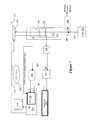
- FIG. 1is a general schematic depicting major components of a laser-based system architecture, 100 , according to the prior art.
- dashed arrowsrepresent optical path, while solid arrows represent electronic signal path.
- the optical paths represented by dashed linesare generally made using fiber optic cables.
- Probing system 100comprises a mode-locked laser source MLL 110 , an optical bench 112 , and data acquisition and analysis apparatus 114 .
- the optical bench 112includes provisions for mounting the DUT 160 and includes beam optics 125 .
- the beam opticsmay include various elements to shape the beam, generally shown as beam manipulation optics, BMO 135 , and elements for pointing and/or scanning the beam over the DUT, such as a laser scanning microscope, LSM 130 .
- a computer 140 or other devicemay be used to provide power and/or signals, 142 , to the DUT 160 , and may provides trigger and clock signals, 144 , to the mode-locked laser source 110 and/or the analysis apparatus 114 .
- the analysis apparatus, 114includes workstation 170 , which controls as well as receives, processes, and displays data from the signal acquisition board 150 and the optical bench 112 .
- computer 140which may be a conventional ATE (Automated Testing Equipment, also known as Automated Testing and Evaluation), generates test vectors that are electrically fed to the DUT.
- the ATEalso sends sync signal to the mode-locked laser source, which emits a laser beam.
- the beam optics 125is then used to point the beam to illuminates various positions on the DUT.
- the beamreflects from the DUT, but the reflection is perturbed by the DUT's response to the test vectors.
- This perturbed reflectionis detected by photodetector 136 , which converts it into an analog signal.
- the analog signalis acquired by the signal acquisition board 150 and is fed to computer 170 , where it is displayed as a waveform corresponding to the perturbed reflection from the DUT. By correlating the timeline of the waveform to that of the ATE, the response of the DUT can be analyzed.
- Various embodiments of the present inventionprovide apparatus and method for laser probing of a DUT to provide modulation information of a selected location or of an area or the entire DUT.
- probing of a DUTis done by applying stimulation signals to the DUT, and illuminating the DUT with a laser beam.
- the reflection of the laser beamis collected and analyzed to provide one or more of the reflection's amplitude, intensity and phase for a selected location.
- probing of a DUTis done by applying stimulation signals to the DUT, and illuminating the DUT with a laser beam.
- the reflection of the laser beamis collected and analyzed to provide a spatial map of one or more of the reflection's amplitude, intensity and phase for each point in a selected area of the DUT.
- Various embodiments of the present inventionfind faults in an integrated circuit by analyzing signals induced on a laser beam reflected from an active region of the device.
- the analysiscan include detecting RF power at a certain bandwidth or bandwidths, demodulating the in-phase and quadrature components of an RF signal, power filtered by a matched filter, and displaying the result either at a fixed position or by creating a spatial map of the induced effect.
- the techniquemay also involve comparing signals from a known good die and from an inspected die.
- Various embodiments of the present inventionsolve the problem of isolating faults in an integrated circuit without making physical contact with the circuit.
- itcan isolate resistive faults between gates without requiring synchronous detection from a tester or stimulus board.
- an apparatus for providing modulation mappingincludes a laser source, a motion mechanism providing relative motion between the laser beam and the DUT, signal collection mechanism, which include a photodetector and appropriate electronics for collecting modulated laser light reflected from the DUT, and a display mechanism for displaying a spatial modulation map which consists of the collected modulated laser light over a selected time period and a selected area of the IC.
- an apparatus for providing modulation mappingwherein a spectrum analyzer is used for generating the modulation mapping.
- an apparatus for providing modulation mappingwherein a lock-in amplifier is used for generating the modulation mapping.
- Various embodiments of the inventionalso provide for a laser scanning mechanism that is operable to scan the selected area to obtain an image of the scanned area, and is operable to scan the selected area to obtain modulation signal from the scanned area.
- the generated imageis then used to normalize the modulation signal and the normalized modulation signal is used to generate a normalized modulation mapping.
- a system for testing an integrated circuit microchip using laser probingcomprises a laser source providing a laser beam; a beam optics receiving said laser beam and focusing said laser beam onto a selected spot on said microchip; a photosensor receiving reflected laser light that is reflected from said microchip and providing an electrical signal; collection electronics receiving the electrical signal from said photosensor and providing an output signal; an analysis system receiving said output signal and providing a total power signal.
- a method for testing an integrated circuitcomprising: stimulating said IC with a test signal; illuminating said IC with a laser beam; collecting beam reflection from said IC; converting said beam reflection to an electrical probing signal; selecting one or more frequencies or a band of frequencies of said probing signal; calculating at least one of total amplitude, total intensity, and phase of said probing signal at the selected frequency or band of frequencies.
- FIG. 1is a general schematic depicting major components of a laser-based IC probe system architecture according to the prior art.
- FIG. 2is a diagram illustrating a first embodiment of the present invention.
- FIG. 3is a diagram illustrating another embodiment of the present invention.
- FIG. 4is a diagram illustrating a fault between two active nodes of a DUT.
- FIGS. 5 a - 5 eare plots illustrating multiplication of probing and reference signals.
- FIG. 6 adepicts a reflectivity map of a DUT
- FIG. 6 bdepicts a modulation map generated according to an embodiment of the invention.
- FIG. 7depicts another embodiment of the present invention.
- FIG. 8depicts yet another embodiment of the present invention.
- FIG. 9is a diagram illustrating the polarization differential probing (PDP) mode for phase detection according to an embodiment of the invention.
- FIG. 10is a diagram illustrating why the laser probing signal modulation is intrinsically polarization sensitive for CMOS transistors due to the asymmetric structure of the CMOS device.
- FIG. 11is an illustration depicting a PDP optical path according to an embodiment of the invention.
- FIG. 12is a plot illustrating the benefit of detecting both return beams of the PDP interferometer.
- FIG. 13illustrates a further embodiment of the invention.
- Various embodiments of the present inventionprovide apparatus and method for testing an integrated circuit.
- integrated circuitsinclude active devices, such as transistors.
- active devicessuch as transistors.
- the subject inventionis based on the inventor's observation that when a transistor is active, it can modulate a light beam illuminating active regions of the transistor. The strength of the modulation depends on the transistor's response to a potential applied to it. Consequently, when a laser beam illuminates the active area, the reflection would be modulated according to the active area's response to applied potential. On the other hand, when the beam illuminates an inactive area, the reflection would not be modulated. Therefore, the study of the beam reflection can provide information regarding the response of active areas to applied potential. It should be noted, however, that while the discussion herein refers to the use of laser beams, other light sources may be used, so long as it is of sufficient energy to enable detection with acceptable signal to noise ratio (SNR) and is sufficiently monochromatic to enable the interaction.
- SNRsignal to noise ratio
- the DUTis provided with test signals, 242 , e.g., from PC 270 .
- the signalmay be a simple square wave at a selected frequency ⁇ .
- laser source 202provides a laser beam 204 .
- a tunable or continuous wave (CW) laser sourcemay be used, although other sources may be used, such as pulsed or mode-locked laser sources.
- beam splitter 206is provided to reflect a small portion of the beam, e.g. 5%, towards optional photodetector 208 .
- the output of photodetector 208is used to monitor the proper operation of the laser source 202 . This feature is beneficial, but is not necessary for the operation of the invention.
- the laser beamis then conditioned and directed onto the DUT 260 by the beam optics 212 .
- the beam opticsmay include beam manipulation optics, BMO 235 for focusing and conditioning the beam to the desired properties.
- Beam optics 212may also include elements 230 for pointing and/or scanning the beam over the DUT. Such element may be, for example, an LSM.
- the beammay be stationary and provisions made for moving or scanning the DUT. This can be achieved by, for example, structuring the DUT holder 232 to function as a controllable X-Y stage. In essence, any structure enabling relative motion between the beam and the DUT is acceptable.
- the reflected beam from the DUTis collected by the beam optics 212 , and is directed towards the photodetector 236 .
- the photodetectorprovides an output, normally an analog electrical signal, that is representative of the reflected light beam.
- the AC component (generally RF) of the photodetector outputis amplified by amplifier 264 (e.g., an RF amplifier), and the amplified signal is provided to a spectrum analyzer 246 .
- the usermay select a specific frequency or a specific band of frequencies, and the spectrum analyzer output the total power, TP, received in the specified frequency or band of frequencies. More specifically, as is shown in callout 244 , the amplified signal has a spread of power P over its frequencies f.
- the usermay select a single frequency f 0 , and the spectrum analyzer would provide the power P 0 of the signal in the selected frequency.
- the usermay select a band of frequencies, ⁇ f, in which case the spectrum analyzer would output a value for the total energy for the selected band.
- the frequency f 0 at which peak power is observedrelates to the frequency ⁇ of the input signal to the DUT.
- P Rthe reflected power
- the frequencyis w 0
- the width of the frequency bandis ⁇ w
- the total integrated poweris given by:
- the total power output, TP, from the spectrum analyzer 246is collected over a specified period of time, e.g., by frame grabber 276 , and the resulting value is provided to the user, e.g., on display 274 of PC 270 .
- the collection over a period of timecan be beneficially obtained by integrating the output of the spectrum analyzer over a specified period of time.
- a spectrum analyzeris used to determine the amount of power in a selected frequency or a band of frequencies of the reflected laser beam. By providing this value for each selected location on the DUT, the functionality of various devices of the DUT can be analyzed. As can be seen, to perform this analysis a simple test signal, such as a simple square wave is sufficient. Consequently, for this testing there is no need to employ an expensive ATE. Rather, one can use the PC 270 to generate the test signal.
- the DC part of the photodetector signalcan be input to a video amplifier 266 .
- the signal of the video amplifier 266can be used to generate a video image to enable navigation over the DUT.
- the signal from the video amplifier 266can be used to normalize the signal from the spectrum analyzer. This feature is particularly beneficial when a scanning of a selected area of the DUT is performed, so as to generate a modulation map.
- the modulation mapis a spatial map upon which the total power at a selected frequency or band of frequencies is indicated for each location of the scanned area.
- the signal from the video amplifier 266can be used to generate a normalized modulation map, i.e., a spatial map upon which the total power at a selected frequency or band of frequencies is indicated for each location on the scanned area, as normalized by the video image signal.
- a normalized modulation mapi.e., a spatial map upon which the total power at a selected frequency or band of frequencies is indicated for each location on the scanned area, as normalized by the video image signal.
- FIG. 3depicts another embodiment of the present invention.
- the embodiment of FIG. 3is similar to that of FIG. 2 , except that the spectrum analyzer has been replaced with a lock-in amplifier. Therefore, the description of the embodiment of FIG. 3 is limited to the feature of the lock-in amplifier, and all elements similar to that of FIG. 2 have the same reference characters as in FIG. 2 .
- the signal from the AC amplifieris fed to the lock-in amplifier.
- a reference signalis also fed to the lock-in amplifier.
- I R (t)the reference signal
- L(t)both signals are multiplied by each other and then integrated, so that the output of the lock-in amplifier is given by:
- the reference signalis of frequency ⁇ , which would typically be set to be the same as that of the AC signal output by the AC amplifier, but phase shifted by a selected amount ⁇ .
- the frequency ⁇relates to the frequency ⁇ of the test signal.
- the signalsare first multiplied by each other, 241 , and the resulting product is integrated, 243 .
- the outputis then collected by the frame grabber 276 , so that a total power value is resulted for each defined period of time. Using this value, the activity of the DUT can be analyzed. As in the embodiment of FIG.
- total power values for multiple locations of a selected area of the DUTcan be obtained and then spatially plotted to provide a modulation map, i.e., a spatial map of the selected area with total power value indicated for each location.
- a modulation mapi.e., a spatial map of the selected area with total power value indicated for each location.
- an image of the DUTcan be obtained and used to normalize the power values, so that a normalized power map can be constructed.
- the embodiment of FIG. 3can also be used to find faults in the DUT by looking at phase shift in the reflected light. More specifically, when a connection from a particular node to an active element is faulty, it can cause delay in the test signal reaching that active element. This is illustrated in FIG. 4 , wherein a fault 405 is depicted as a resistive element between active elements 400 and 410 . Under such circumstances, the active device 410 would respond once the signal is received, but the response would be delayed in time. Such faults cannot be easily detected using conventional techniques, such as OBIRCH or static emission, and would require exact synchronization with a tester, such as an ATE, to be detected using dynamic emission testers. However, using the embodiment of FIG. 3 , no synchronization is needed and the test signal may be a simple sine or square wave signal.
- the faulty connectionWhen the test signal has a periodic format, such as a sine or square wave signal, the faulty connection would cause a delay in the signal reaching the device, and the device would respond in a delayed manner. Consequently, if a laser beam illuminates the device, the reflected beam would be modulated periodically at the same frequency as the test signal, but it would be phase shifted. This phase shift can be detected using the embodiment of FIG. 3 , since a phase shift in the input signal to the lock-in amplifier would cause a change in the product signal resulting from the multiplication of the input and reference signal. Lock-in and frequency demodulation techniques are well known in the art.
- FIG. 3The operation of the embodiment of FIG. 3 can be understood from the following description with reference to the plots of FIGS. 5 a - 5 e .
- the test signalis a sine wave of frequency ⁇ ( ⁇ t) as shown in FIG. 5 a
- the reflected laser beamwill be modulated at the same frequency so that the signal input to the lock-in amplifier also has frequency ⁇ .
- the reference signalis also a sine wave of frequency ⁇ and same phase as the input signal, then the multiplication of the input and reference signals results in the signal shown on plot 5 b . If, however, the reference signal is shifted by ⁇ /2, then the resulting product is as shown in FIG. 5 c , which will integrate to zero.
- the reference signalit is beneficial to set the reference signal at the same frequency, but shifted by ⁇ /4, so that the resulting product is as shown by FIG. 5 d . Then, whenever the laser beam is placed over an active region, the resulting product will be as shown in FIG. 5 d and the integration of that product over a specified period will result in a given value.
- This valuecan be displayed, compared to a known value calculated or experimentally obtained from a known properly functional region, or compared to values obtain from other active regions on the same or different DUT. If the value deviates by a more than an allowable amount, then the active region can be flagged as faulty.
- the RF signal on the reflected laser beamwould be phase shifted.
- the reference signalis kept at ⁇ /4 shift from the proper, un-shifted detector signal.
- the signal from the reflected beamis also shifted, in this example by ⁇ /1.2, then the resulting plot shifts vertically, which would cause a change in the integrated value. This change can be used to detect faulty active regions on the DUT.
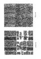
- FIG. 6 adepicts an image of transistors in an integrated circuit obtained using the inventive system to map reflected light intensity, i.e., the image is constructed using the output from a video amplifier, such as, video amplifier 266 shown in FIG. 2 .
- a video amplifiersuch as, video amplifier 266 shown in FIG. 2 .
- FIG. 6 bdepicts modulation map, showing activity of various devices within the DUT at a particular frequency of interest.
- the modulation datawas acquired simultaneously with the image of FIG. 6 a and a spectrum analyzer was employed.
- higher grayscale valuesindicate larger modulation signal, i.e., active regions.
- the DUTwas driven with 100 MHz clock, and the spectrum analyzer was tuned to 100 MHz frequency.
- FIG. 7depicts another embodiment of the subject invention.
- the embodiments of FIGS. 2 and 3rely mainly on amplitude modulation of the laser beam.
- the embodiment of FIG. 7is designed to detect phase modulation of the laser beam. Therefore, while the system of FIG. 7 is similar to that of FIGS. 2 and 3 , the embodiment of FIG. 7 also employ a phase to amplitude converter 292 .
- the output of the phase to amplitude converter 292is applied to the photodetector 236 and is amplified by RF amplifier 264 .
- the amplified signalis then provided to the analyzer 248 , which may be a spectrum analyzer, a lock-in amplifier, etc., as explained with respect to FIGS. 2 and 3 .
- the phase to amplitude converter 292may be any conventional converter, such as a Michelson interferometer, spatial differential interferometer, time differential prober, etc. Such systems are described in U.S. patent application Ser. No. 11/169,423, commonly assigned to the present assignee, which is incorporated herein by reference in its entirety.
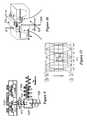
- FIG. 8illustrates another embodiment of the subject invention.
- the embodiment of FIG. 8is similar to that of FIG. 7 , except that a polarization differential probing (PDP) optics, 800 , is used as a phase to amplitude converter.
- PDPpolarization differential probing
- the systemoperates as follows.
- the DUT 860is stimulated with test signals from stimulus 862 , which may be a stand alone equipment or part of computer 870 . If the stimulus 862 is a stand alone device, it is beneficial to provide a communication link between the computer 870 and the stimulus 862 , as shown.
- laser source 802provides laser beam 804 .
- a small portion of the laser beamis deflected by polarizing beam splitter 806 and is detected by photodetector 808 so as to monitor the operation of the laser source 802 .
- the remainder of the laser beampasses through polarizing beam splitter 803 and enters a Faraday rotator 805 .
- the beamthen passes through another polarizer beam splitter 806 .
- the beamis actually composed of two orthogonal polarization states, or two co-located beams polarized at 90° to each other.
- Both beamsthen enters a scanning mechanism 830 , which may be an LSM, AOD (acoustic-optical deflector), scanning lens, tube lens, etc.
- an LSM 830is used, which is controlled by computer 870 .
- the beamsthen passes a variable retarder 807 , which retards only one of the beams. This beam retardation is shown schematically in FIG. 8 by the double-headed arrow.
- Both beamsthen pass through the objective lens 809 and enter the DUT 860 .
- the objective lens 809may be a simple single lens, or a combination of lenses optionally including a solid immersion lens (SIL) 811 .
- One or both beamsmay be modulated by the DUT upon reflection; however, as will be explained further below, the inventors have observed that the beams are modulated by a different amount.
- the reflected beamspass through the objective lens 809 and enter the variable retarder 807 , wherein an additional retardation is introduced.
- half of each beamis deflected by the polarizer beam splitter 806 towards photodetector 836 , and the remaining half is passed through the Faraday rotator 805 and is deflected by the polarizer beam splitter 803 towards photodetector 837 .
- each photodetectoris an avalanche photodiode (APD).
- the output from photodetector 836is applied to bias T 1 , while the output of photodetector 837 is applied to bias T 2 .
- the DC component of the signalis routed to video amplifier 866 and to frame grabber 876 to generate an image of the DUT.
- Another optionis to have the DC component of the signal of bias T 2 also routed to video amplifier 867 and to frame grabber 876 to generate another image of the DUT.
- the AC part of each signalis amplified by RF amplifiers 864 , 868 , and the signal is applied to selector 877 .
- Selector 877provides an output that may be a summation/difference of both signals, the signal of T 1 only, or the signal of T 2 only.
- the output of the selector 877is then applied to the analyzer 848 , which may be a spectrum analyzer, lock-in amplifier, etc., as explained with respect to FIGS. 2 and 3 .
- FIG. 9is a diagram illustrating the polarization differential probing (PDP) mode for phase detection, as can be employed in the embodiments of FIGS. 7 and 8 .
- a laser beam 920 from a single modulated laser sourceis split into two orthogonally polarizes laser beams 922 , 924 , by beam optics 925 . Both beams 922 , 924 traverse the same optical path, but have orthogonal linear polarization states as depicted by the dots and arrows.
- both beamsare made to incident on the same point 932 on the DUT 910 .
- both beamsare made to be incident on the DUT 910 at nominally the same time.
- the polarization directions of the beams 922 , 924are aligned with the transistor gate width and length directions in the DUT 910 .
- This polarization differenceresults in phase modulation differences between the two beams after DUT interaction, as will be demonstrated below with reference to FIG. 10 .
- the two beams 922 , 924are made to interfere 926 after their DUT interactions in order to convert their phase variations into amplitude variations that can be detected using photosensors.
- a differential detection schemecan be optionally employed to increase signal modulation.
- FIG. 10is a diagram illustrating why the laser probing signal modulation is intrinsically polarization sensitive for MOS transistors due to the intrinsic asymmetry of the MOS device.
- a laser beam 1020is incident from the bottom (through the silicon substrate).
- the laser beam's polarization stateshould be aligned parallel to the direction of the strong modulating fields in the gate/drain regions of the transistor, i.e., along the gate length direction (along E x in FIG. 10 ).
- the Plasma-Optical effectrequires the laser beam to drive the charge carriers induced under the gate.
- the present inventorsrealized that, unlike the prior art interferometric arrangements, the reference beam need not traverse a reference path separate from the probing path. Rather, it is possible to have both reference and probing beams traverse the same path and be pointed onto the same point on the DUT at nominally the same time, while still obtaining an interferometric effect that correlates to the DUT's response to the stimulating signal.
- reference beamand “probing beam” is for convenience purposes only, since it should be apparent that unlike the prior art, here both beams illuminate the exact same area to be investigated at nominally the same time and, therefore, in this sense, each beam can be both a reference and a probing beam.
- FIG. 11is an illustration depicting a common-path PDP optical arrangement according to an embodiment of the invention. While in actuality the incident beam and the reflected beam traverse the same elements, for better understanding the illustration is divided into two optical paths, showing each optical element twice.
- the top pathis the incident beam path originating from the laser source, while the bottom path is the reflected beam path.
- the incident beamtravels from left to right in the illustration.
- vertically oriented arrowsindicate a vertically polarized beam while dots indicate a horizontally polarized beam.
- a tilted arrowindicates a beam that is linearly polarized at some angle off the vertical. Spatial separation between a dot and an arrow depicts a phase difference between the two beams.
- the beam from the modulated laser sourceenters the first polarizing beam splitter PBS 1 so that part of the beam is deflected towards light sensor 1110 . This deflection may be set at 5% or so.
- the output of the sensor 1110is used to monitor the beam's intensity and is not part of the PDP optics, but is rather an optional intensity monitor.
- the remaining part of the beam that passes through the first PBS cube (PBS 1 )enters the second polarizing beam splitters PBS 2 , which is oriented to pass only a vertically oriented beam.
- the beam's polarization stateis rotated a predetermined amount so as to generate a rotated polarized beam that is an equivalent of a superposition of a vertically polarized beam and a horizontally polarized beam.
- the beamis rotated 45 degrees from the vertical by the action of the Faraday rotator (FR) and the third PBS cube (PBS 3 ) is oriented to transmit the rotated beam. Consequently, at this stage the beam is the equivalent of a superposition of a vertically polarized beam and a horizontally polarized beam, both beams equal in amplitude and in phase with each other. If the amplitude of the beam should not be set to equal, the rotation should be to a different angle.
- the dashed callout circles in the incident beam path, between PBS 3 and VR,indicate the equivalence between a 45-degree polarized beam and two in-phase, equal amplitude beams, one polarized vertically and the other horizontally.
- the rotationmay be to other than 45 degrees, in which case the equivalence would be of two, in-phase beams, one polarized vertically and the other horizontally, but having different amplitude.
- the two beamsthen enter the variable retarder VR.
- the fast and slow axes of the variable-retarder (VR)are aligned along these vertical and horizontal polarization directions.
- the beamconsists of two spatially coincident, equal-amplitude, orthogonally polarized beams that are phase-shifted (retarded) with respect to each other by a small amount (nominally, ⁇ /4). This is indicated in the illustration by the dot being slightly behind the vertical arrow, representing a retardation of the horizontally polarized beam relative to the vertically polarized beam.
- the two beamsare then focused onto the same point on the DUT by the objective lens OL.
- the DUTis oriented such that the polarization directions of these two beams are aligned with the length and width directions of the transistor gates. Interaction with the DUT phase modulates one of the beams relative to the other by a small amount. In this manner, the beam being modulated by the DUT may be thought of as the probing beam, while the other beam may be thought of as the reference beam.
- the beam being modulated by the DUTmay be thought of as the probing beam, while the other beam may be thought of as the reference beam.
- the beamstraverses a reference optical path, but rather both beams traverse the identical path to the probing location. Therefore, as noted before, in this sense there is no reference beam and probing beam, but for convenience one may refer to one beam as the reference beam and the other as the probing beam.
- the two linearly polarized beamsretrace their path to the VR.
- the phase modulation induced on the beams by the DUTis typically much smaller than the phase shift induced by passage through VR and so is not explicitly shown here.
- Passing through the VRintroduces an addition phase-shift between the two returned reference and probing beams (now nominally phase-shifted by ⁇ /2).
- PBS 3a portion of each beam is reflected and sent to photosensor 1120 , and the other portion is transmitted. The reflected portions interfere, since they are now in the same polarization state, and generate the reflected-A signal.
- only one photosensor 1120is used and its output is collected by the receiver electronics and analyzed, as described in more detail below.
- the transmitted portionsare deflected out of the beam path via the action of FR and PBS 2 so as to be detected by a second photosensor 1130 .
- the transmitted halvesalso interfere since they are also in the same polarization state, generating the reflected-B signal.
- the reflected-B signalis collected by the receiver electronics and is analyzed, as described in more details below.
- ⁇ termaccounts for the static phase shift introduced by the double-pass through the variable rotator, VR, while the ⁇ term is the small varying relative phase shift of the two beams resulting from the interaction with the DUT as it undergoes testing.
- Similar analysis for the reflected-B signalresults in: R(B) ⁇ (E x / ⁇ 2) 2 +(E y / ⁇ 2) 2 +2[(E x / ⁇ 2)(E y / ⁇ 2)]Cos( ⁇ + ⁇ ) Eqn 4.
- Eqn. 3 and Eqn. 4are plotted in FIG. 12 . From this plot, it is clear that setting the static phase shift, ⁇ , to ⁇ /2 (quarter waver condition for the round trip beam) gives maximum sensitivity to changes in ⁇ and makes the two signals nominally equal in intensity. Under this condition, Eqn. 3 and Eqn. 4 simplify, respectively, to: R(A) ⁇ (1/2)E x 2 +(1/2)E y 2 +E x E y Sin ( ⁇ ) Eqn. 5. and R(B) ⁇ (1/2)E x 2 +(1/2)E y 2 ⁇ E x E y Sin ( ⁇ ) Eqn. 6. Then, R(A) ⁇ R(B) ⁇ 2 E x E y Sin ( ⁇ ) Eqn. 7.
- both reference and probing beamstraverse the identical optical path and are pointed to the same location on the DUT at nominally the same time, it means that this scheme has better phase noise immunity then prior art interferometric systems.
- both beamsare subject to the same vibrations and optical losses. This eliminates or reduces the need for active vibration compensation, path length matching, and power matching of the two arms of the interferometer.
- the two photodiodesmay be used in a differential detection mode.
- one diodeproduces a positive going signal at its amplifier input, while the other one produces a negative signal.
- the biasis to about ⁇ 60V and +60V, respectively.
- Summing the two output signalse.g., by selector 877 , produces an enhanced differential signal. Monitoring the current of both APD's assists in checking the balance of the PDP optics, as the variable phase plate of the PDP can be adjusted until the same current is observed by the two current monitors 898 and 894 .
- the signal from only one APDis required.
- the signal from each photosensoris also sent to a video amplifier, which provides a video out signal for processing and display.
- the variable retardermay be varied to tune the retardation so that the image contrast is varied to the desired result.
- imagingmay be performed using both APD's and the resulting images subtracted from each other so as to obtain a difference image.
- the APD's gainmay be advantageously controlled to, first, balance the APD's response and, second, to improve the imaging.
- the voltage/gain response of each APDcan be determined.
- the gain of each APDcan be controlled to a desired value by selecting the appropriate voltage on the corresponding power supply.
- the following proceduremay be used. First, the voltage of the power supplies of each APD is set to result in the same gain provided by both APD's, thereby balancing the output of the APD's. Alternatively, if a different gain circuitry is used, it should be balanced to obtained balanced output.
- variable wave plateis adjusted until the current output of both ADP's is the same, thereby balancing the optical path.
- the variable gaincan also be used for improved imaging. For example, when the image scan goes from a relatively dark area to a relatively bright area, the gain of the APD's may be reduced so as not to saturate the image. Conversely, when moving from a bright area to a dark area, the gain may be increased to provide improved contrast and detail.
- FIG. 13depicts a block diagram of another embodiment of the invention, wherein the signals are digitized individually. This allows the signals to be summed, subtracted, divided, etc. It also gives greater flexibility. For example, the ratio of reflected A/reflected B gives pure PDP signal, but this arrangement also enables other ratios, such as reflected A/Incident pick-off and/or reflected B/Incident pick-off simultaneously. The user may try various signals and then chose which provides the best result for a particular investigation.
- a computersuch as a programmed personal computer PC 1300 is equipped with a digital signal processing card DSP 1310 and a frame grabber 1320 .
- DSP 1310digital signal processing card
- three channels, CH 1 , CH 2 , and CH 3provide signals to the DSP 1310 .
- Channel CH 1is optional and is used to monitor the operation of the laser source.
- Channel 1comprises photosensor 1331 which receives a light signal from a fiber optics and outputs an electrical signal. The electrical output of the photosensor 1331 is applied to current to voltage converter 1341 which has variable transimpedance gain control. The output of the current to voltage converter is then applied to a gated integrator 1351 , which is responsive to a gate-on signal.
- the signal from the gated integrator 1351is applied to a variable gain/offset circuit 1361 to enable gain/offset control.
- the signal from the gain/offset circuitry 1361is then applied to a digital/analog converter DAC 1371 to convert the analog signal into a digital signal.
- Variable gain/offset circuit 1361allows the signal applied to DAC 1371 to be within the input range of the DAC.
- a 14 bit DAC converter with internal sample/hold featureis used.
- the digital outputis then provided to the DSP card for processing.
- channel CH 1is used to monitor the output of the laser source and it receives the signal from the pick-off fiber as explained above.
- Channels CH 2 and CH 3are used for the probing and receive the reflected signals Reflected-A and Reflected-B, respectively.
- one of the channels, in this illustration channel CH 3is also used for imaging by applying the output of its current to voltage converter to a video amplifier 1380 , the output of which is applied to the frame grabber 1320 .
- the quality of the imagemay be adjusted by a brightness/contrast (or black level/gain) signal applied to the video amplifier.
- channels CH 2 and CH 3can be identical.
- Each channelreceives signal from a fiber optics and a photodetector, 1332 , 1333 , converts the optical signal to an analog signal.
- the analog signalis amplified by the RF amplifier, 1352 , 1353 , and is input to an analyzer, 1362 , 1363 .
- the analyzermay be a spectrum analyzer as explained with respect to FIG. 2 or a lock-in amplifier, as explained with respect to FIG. 3 .
- the output from the analyzeris digitized and supplied to the DSP card 1310 .
- the signal from the analyzeris input to the DSP card, as it may provide a higher resolution than the frame grabber.
- the beamalso allows for the beam to be set in a fixed x-y position while data is being acquired for a single spot on the DUT as the DUT is being stimulated with variable stimulus signal. This can be done repeatedly for various locations on the DUT.
- a series of modulation mapscan be generated, one for each modulation signal.
- the series of mapscan also be plotted into a 3-D plot with the DUT stimulus parameter plotted in, say, the Z-direction. Further investigations can be performed by generating cross sections of the 3-D plots.
- the output of each analyzercan be input to more than one channel. This enables, for example, to provide simultaneous maps of amplitude and phase over the selected area of the DUT.
- one channelsay CH 2 can be used to generate a power map, while the other to generate a phase map.
Landscapes
- Engineering & Computer Science (AREA)
- Physics & Mathematics (AREA)
- General Engineering & Computer Science (AREA)
- General Physics & Mathematics (AREA)
- Computer Hardware Design (AREA)
- Microelectronics & Electronic Packaging (AREA)
- Health & Medical Sciences (AREA)
- Computer Vision & Pattern Recognition (AREA)
- Electromagnetism (AREA)
- Toxicology (AREA)
- Tests Of Electronic Circuits (AREA)
Abstract
Description
R(A)∝(Ex/√2)2+(Ey/√2)2−2[(Ex/√2)(Ey/√2)]Cos(θ+δ)
R(B)∝(Ex/√2)2+(Ey/√2)2+2[(Ex/√2)(Ey/√2)]Cos(θ+δ)
R(A)∝(1/2)Ex2+(1/2)Ey2+ExEySin (δ) Eqn. 5.
and
R(B)∝(1/2)Ex2+(1/2)Ey2−ExEySin (δ) Eqn. 6.
Then,
R(A)−R(B)∝2 ExEySin (δ) Eqn. 7.
Claims (29)
Priority Applications (6)
| Application Number | Priority Date | Filing Date | Title |
|---|---|---|---|
| US11/438,121US7733100B2 (en) | 2005-08-26 | 2006-05-18 | System and method for modulation mapping |
| JP2006227759AJP2007064975A (en) | 2005-08-26 | 2006-08-24 | Modulation map display system and method |
| US12/534,069US7990167B2 (en) | 2005-08-26 | 2009-07-31 | System and method for modulation mapping |
| US13/095,831US8686748B2 (en) | 2005-08-26 | 2011-04-27 | System and method for modulation mapping |
| US13/657,666US9239357B2 (en) | 2005-08-26 | 2012-10-22 | System and method for modulation mapping |
| US14/997,460US9915700B2 (en) | 2005-08-26 | 2016-01-15 | System and method for modulation mapping |
Applications Claiming Priority (2)
| Application Number | Priority Date | Filing Date | Title |
|---|---|---|---|
| US71182205P | 2005-08-26 | 2005-08-26 | |
| US11/438,121US7733100B2 (en) | 2005-08-26 | 2006-05-18 | System and method for modulation mapping |
Related Child Applications (1)
| Application Number | Title | Priority Date | Filing Date |
|---|---|---|---|
| US12/534,069DivisionUS7990167B2 (en) | 2005-08-26 | 2009-07-31 | System and method for modulation mapping |
Publications (2)
| Publication Number | Publication Date |
|---|---|
| US20070046301A1 US20070046301A1 (en) | 2007-03-01 |
| US7733100B2true US7733100B2 (en) | 2010-06-08 |
Family
ID=37803212
Family Applications (5)
| Application Number | Title | Priority Date | Filing Date |
|---|---|---|---|
| US11/438,121Active2027-04-05US7733100B2 (en) | 2005-08-26 | 2006-05-18 | System and method for modulation mapping |
| US12/534,069ActiveUS7990167B2 (en) | 2005-08-26 | 2009-07-31 | System and method for modulation mapping |
| US13/095,831Active2027-05-03US8686748B2 (en) | 2005-08-26 | 2011-04-27 | System and method for modulation mapping |
| US13/657,666Active2027-12-21US9239357B2 (en) | 2005-08-26 | 2012-10-22 | System and method for modulation mapping |
| US14/997,460Active2026-06-12US9915700B2 (en) | 2005-08-26 | 2016-01-15 | System and method for modulation mapping |
Family Applications After (4)
| Application Number | Title | Priority Date | Filing Date |
|---|---|---|---|
| US12/534,069ActiveUS7990167B2 (en) | 2005-08-26 | 2009-07-31 | System and method for modulation mapping |
| US13/095,831Active2027-05-03US8686748B2 (en) | 2005-08-26 | 2011-04-27 | System and method for modulation mapping |
| US13/657,666Active2027-12-21US9239357B2 (en) | 2005-08-26 | 2012-10-22 | System and method for modulation mapping |
| US14/997,460Active2026-06-12US9915700B2 (en) | 2005-08-26 | 2016-01-15 | System and method for modulation mapping |
Country Status (2)
| Country | Link |
|---|---|
| US (5) | US7733100B2 (en) |
| JP (1) | JP2007064975A (en) |
Cited By (8)
| Publication number | Priority date | Publication date | Assignee | Title |
|---|---|---|---|---|
| US20100289488A1 (en)* | 2009-05-14 | 2010-11-18 | Joseph Martin Patterson | Optical-Magnetic Kerr Effect Waveform Testing |
| US7956625B1 (en)* | 2006-10-31 | 2011-06-07 | Dcg Systems, Inc. | Undoped silicon heat spreader window |
| US20110199110A1 (en)* | 2005-08-26 | 2011-08-18 | Dcg Systems, Inc. | System and method for modulation mapping |
| US8723140B2 (en) | 2011-08-09 | 2014-05-13 | Palo Alto Research Center Incorporated | Particle analyzer with spatial modulation and long lifetime bioprobes |
| US9099350B2 (en) | 2011-05-31 | 2015-08-04 | Hamamatsu Photonics K.K. | Apparatus for inspecting integrated circuit |
| US20160161556A1 (en)* | 2014-08-12 | 2016-06-09 | Globalfoundries Singapore Pte. Ltd. | Defect isolation methods and systems |
| US9417281B1 (en) | 2014-09-30 | 2016-08-16 | Checkpoint Technologies Llc | Adjustable split-beam optical probing (ASOP) |
| US10139447B2 (en) | 2014-04-24 | 2018-11-27 | Hamamatsu Photonics K.K. | Image generation apparatus and image generation method |
Families Citing this family (44)
| Publication number | Priority date | Publication date | Assignee | Title |
|---|---|---|---|---|
| KR100846098B1 (en)* | 2006-10-10 | 2008-07-14 | 삼성전자주식회사 | How to set up defect inspection conditions |
| US9164037B2 (en) | 2007-01-26 | 2015-10-20 | Palo Alto Research Center Incorporated | Method and system for evaluation of signals received from spatially modulated excitation and emission to accurately determine particle positions and distances |
| US8821799B2 (en) | 2007-01-26 | 2014-09-02 | Palo Alto Research Center Incorporated | Method and system implementing spatially modulated excitation or emission for particle characterization with enhanced sensitivity |
| WO2009036802A1 (en)* | 2007-09-20 | 2009-03-26 | Ecole polytechnique fédérale de Lausanne (EPFL) | Integrated receiving circuit and method for radiofrequency and high speed signals |
| US7894068B2 (en)* | 2008-02-04 | 2011-02-22 | Palo Alto Research Center Incorporated | Producing filters with combined transmission and/or reflection functions |
| US7701580B2 (en) | 2008-02-01 | 2010-04-20 | Palo Alto Research Center Incorporated | Transmitting/reflecting emanating light with time variation |
| US8153949B2 (en)* | 2008-12-18 | 2012-04-10 | Palo Alto Research Center Incorporated | Obtaining sensing results indicating time variation |
| US8263955B2 (en)* | 2008-12-18 | 2012-09-11 | Palo Alto Research Center Incorporated | Causing relative motion |
| US8373860B2 (en)* | 2008-02-01 | 2013-02-12 | Palo Alto Research Center Incorporated | Transmitting/reflecting emanating light with time variation |
| US8629981B2 (en)* | 2008-02-01 | 2014-01-14 | Palo Alto Research Center Incorporated | Analyzers with time variation based on color-coded spatial modulation |
| SG10201401887YA (en)* | 2009-05-01 | 2014-06-27 | Dcg Systems Inc | Systems and method for laser voltage imaging state mapping |
| FR2978831A1 (en)* | 2011-08-05 | 2013-02-08 | St Microelectronics Sa | DEFECT DETECTION THROUGH FREQUENCY IMAGING. |
| US9029800B2 (en) | 2011-08-09 | 2015-05-12 | Palo Alto Research Center Incorporated | Compact analyzer with spatial modulation and multiple intensity modulated excitation sources |
| US9714978B2 (en)* | 2012-04-12 | 2017-07-25 | Larry Ross | At-speed integrated circuit testing using through silicon in-circuit logic analysis |
| TWI479167B (en)* | 2012-05-16 | 2015-04-01 | Dcg Systems Inc | System and method laser-assisted device alteration using synchronized laser pulses |
| JP6166032B2 (en) | 2012-11-06 | 2017-07-19 | 浜松ホトニクス株式会社 | Semiconductor device inspection apparatus and semiconductor device inspection method |
| US10180402B2 (en)* | 2012-12-14 | 2019-01-15 | Sri International | Method and apparatus for conducting automated integrated circuit analysis |
| US9618563B2 (en) | 2013-02-01 | 2017-04-11 | Hamamatsu Photonics K.K. | Semiconductor device inspection device and semiconductor device inspection method |
| US10838406B2 (en) | 2013-02-11 | 2020-11-17 | The Aerospace Corporation | Systems and methods for the patterning of material substrates |
| US10613513B2 (en)* | 2013-02-11 | 2020-04-07 | The Aerospace Corporation | Systems and methods for modifying material substrates |
| WO2014160618A1 (en)* | 2013-03-24 | 2014-10-02 | Dcg Systems, Inc. | Pulsed lada for acquisition of timing diagrams |
| JP6283501B2 (en)* | 2013-11-12 | 2018-02-21 | 浜松ホトニクス株式会社 | Frequency analysis apparatus and frequency analysis method |
| JP6283507B2 (en) | 2013-11-29 | 2018-02-21 | 浜松ホトニクス株式会社 | Semiconductor device measuring apparatus and semiconductor device measuring method |
| JP2015175851A (en)* | 2014-03-13 | 2015-10-05 | ディーシージー システムズ、 インコーポライテッドDcg Systems Inc. | System and method for fault isolation by emission spectra analysis |
| JP2016109673A (en)* | 2014-10-16 | 2016-06-20 | ディーシージー システムズ、 インコーポレイテッドDcg Systems Inc. | Systems and method for laser voltage imaging |
| KR20170040778A (en)* | 2015-10-05 | 2017-04-13 | 에프이아이 컴파니 | Optimized wavelength photon emission microscope for vlsi devices |
| CN108603845B (en)* | 2015-11-06 | 2019-12-03 | Fei 公司 | For testing the system and diagnosing and measuring method of circuit |
| JP6194380B2 (en)* | 2016-02-29 | 2017-09-06 | 浜松ホトニクス株式会社 | Integrated circuit inspection equipment |
| JP6714485B2 (en) | 2016-09-28 | 2020-06-24 | 浜松ホトニクス株式会社 | Semiconductor device inspection method and semiconductor device inspection apparatus |
| JP6820184B2 (en)* | 2016-10-26 | 2021-01-27 | 浜松ホトニクス株式会社 | Semiconductor device inspection method and semiconductor device inspection equipment |
| JP6898211B2 (en)* | 2017-11-27 | 2021-07-07 | 浜松ホトニクス株式会社 | A recording medium for recording an optical measurement method, an optical measurement device, an optical measurement program, and an optical measurement program. |
| US11579184B2 (en) | 2017-11-27 | 2023-02-14 | Hamamatsu Photonics K.K. | Analysis method, analysis device, analysis program, and recording medium for recording analysis program |
| US20190287762A1 (en) | 2018-01-25 | 2019-09-19 | Fei Company | System and method of preparing integrated circuits for backside probing using charged particle beams |
| JP6603766B2 (en)* | 2018-08-06 | 2019-11-06 | 浜松ホトニクス株式会社 | Image generating apparatus and image generating method |
| RU2685350C1 (en)* | 2018-08-08 | 2019-04-17 | Федеральное государственное бюджетное образовательное учреждение высшего образования "Волгоградский государственный технический университет" (ВолгГТУ) | Water-oil-swelling elastomer composition |
| US11079432B2 (en)* | 2019-02-19 | 2021-08-03 | Nxp B.V. | Integrated laser voltage probe pad for measuring DC or low frequency AC electrical parameters with laser based optical probing techniques |
| CN110111537B (en)* | 2019-04-29 | 2021-08-10 | 深圳市科迈爱康科技有限公司 | Early warning method and device applied to snowfield exploration and intelligent shoes |
| SG11202111416YA (en)* | 2019-05-31 | 2021-11-29 | Hamamatsu Photonics Kk | Semiconductor apparatus examination method and semiconductor apparatus examination apparatus |
| JP7164488B2 (en) | 2019-05-31 | 2022-11-01 | 浜松ホトニクス株式会社 | Semiconductor device inspection method and semiconductor device inspection apparatus |
| US11125815B2 (en)* | 2019-09-27 | 2021-09-21 | Advanced Micro Devices, Inc. | Electro-optic waveform analysis process |
| JP7608469B2 (en)* | 2020-09-23 | 2025-01-06 | 浜松ホトニクス株式会社 | Inspection Equipment |
| WO2023002688A1 (en) | 2021-07-19 | 2023-01-26 | 浜松ホトニクス株式会社 | Semiconductor error analysis device and semiconductor error analysis method |
| KR20240036501A (en) | 2021-07-19 | 2024-03-20 | 하마마츠 포토닉스 가부시키가이샤 | Semiconductor failure analysis device and semiconductor failure analysis method |
| CN114614892B (en)* | 2022-05-11 | 2023-03-31 | 南京信息工程大学 | Optical information transmission system based on plasma spectrum |
Citations (68)
| Publication number | Priority date | Publication date | Assignee | Title |
|---|---|---|---|---|
| US3524694A (en) | 1965-11-26 | 1970-08-18 | Leitz Ernst Gmbh | Flat-field micro objective with increased magnification |
| US3711186A (en) | 1970-02-10 | 1973-01-16 | Vickers Ltd | Microscope objectives |
| US3912378A (en) | 1973-02-08 | 1975-10-14 | Olympus Optical Co | Oil immersion apochromatic microscope objective |
| US4297032A (en) | 1980-02-14 | 1981-10-27 | The United States Of America As Represented By The Secretary Of The Navy | Dark field surface inspection illumination technique |
| UST102104I4 (en) | 1978-12-29 | 1982-08-03 | Kirk Joseph P | Scanning optical system adapted for linewidth measurement in semiconductor devices |
| US4353618A (en) | 1978-11-09 | 1982-10-12 | Ernst Leitz Wetzlar Gmbh | Optical arrangement for the reflecting microscopic examination of an object |
| US4555767A (en) | 1982-05-27 | 1985-11-26 | International Business Machines Corporation | Method and apparatus for measuring thickness of epitaxial layer by infrared reflectance |
| US4588950A (en) | 1983-11-15 | 1986-05-13 | Data Probe Corporation | Test system for VLSI digital circuit and method of testing |
| US4615620A (en) | 1983-12-26 | 1986-10-07 | Hitachi, Ltd. | Apparatus for measuring the depth of fine engraved patterns |
| US4625114A (en) | 1985-07-15 | 1986-11-25 | At&T Technologies, Inc. | Method and apparatus for nondestructively determining the characteristics of a multilayer thin film structure |
| US4634234A (en) | 1983-05-02 | 1987-01-06 | Jenoptik Jena G.M.B.H. | Front lens group for immersion microscope objective in BD versions of high aperture |
| US4680635A (en) | 1986-04-01 | 1987-07-14 | Intel Corporation | Emission microscope |
| US4681449A (en) | 1984-09-07 | 1987-07-21 | Stanford University | High speed testing of electronic circuits by electro-optic sampling |
| US4698587A (en) | 1985-03-28 | 1987-10-06 | The United States Of America As Represented By The Secretary Of The Air Force | Method of characterizing critical timing paths and analyzing timing related failure modes in very large scale integrated circuits |
| US4721910A (en) | 1986-09-12 | 1988-01-26 | American Telephone And Telegraph Company, At&T Bell Laboratories | High speed circuit measurements using photoemission sampling |
| US4724322A (en) | 1986-03-03 | 1988-02-09 | Applied Materials, Inc. | Method for non-contact xyz position sensing |
| US4736159A (en) | 1985-05-21 | 1988-04-05 | Matsushita Electric Industrial Co., Ltd. | Laser probing for solid-state device |
| US4758092A (en) | 1986-03-04 | 1988-07-19 | Stanford University | Method and means for optical detection of charge density modulation in a semiconductor |
| US4758786A (en) | 1986-08-06 | 1988-07-19 | Molecular Devices Corporation | Method of analyzing semiconductor systems |
| US4811090A (en) | 1988-01-04 | 1989-03-07 | Hypervision | Image emission microscope with improved image processing capability |
| US4908568A (en) | 1987-06-09 | 1990-03-13 | Siemens Aktiengesellschaft | Mechanical probe for optical measurement of electrical potentials |
| US4956603A (en) | 1988-03-29 | 1990-09-11 | Sgs-Thomson Microelectronics S.R.L. | Method and apparatus for measuring the lifetime on P-N semiconductor junctions by photovoltaic effect |
| US4968932A (en) | 1987-09-30 | 1990-11-06 | Kabushiki Kaisha Toshiba | Evaluation method for semiconductor device |
| US5004307A (en) | 1990-04-12 | 1991-04-02 | The Board Of Trustees Of The Leland Stanford Junior University | Near field and solid immersion optical microscope |
| US5010945A (en) | 1988-11-10 | 1991-04-30 | Lanxide Technology Company, Lp | Investment casting technique for the formation of metal matrix composite bodies and products produced thereby |
| US5087121A (en) | 1987-12-01 | 1992-02-11 | Canon Kabushiki Kaisha | Depth/height measuring device |
| US5208648A (en) | 1991-03-11 | 1993-05-04 | International Business Machines Corporation | Apparatus and a method for high numerical aperture microscopic examination of materials |
| US5220403A (en) | 1991-03-11 | 1993-06-15 | International Business Machines Corporation | Apparatus and a method for high numerical aperture microscopic examination of materials |
| US5247392A (en) | 1991-05-21 | 1993-09-21 | Siemens Aktiengesellschaft | Objective lens for producing a radiation focus in the inside of a specimen |
| US5282088A (en) | 1992-10-19 | 1994-01-25 | Mark Davidson | Aplanatic microlens and method for making same |
| US5334540A (en) | 1991-11-14 | 1994-08-02 | Mitsubishi Denki Kabushiki Kaisha | OBIC observation method and apparatus therefor |
| US5412328A (en) | 1992-12-31 | 1995-05-02 | United Technologies Corporation | Non-contact current injection apparatus and method for use with linear bipolar circuits |
| US5430305A (en)* | 1994-04-08 | 1995-07-04 | The United States Of America As Represented By The United States Department Of Energy | Light-induced voltage alteration for integrated circuit analysis |
| US5430292A (en)* | 1991-06-10 | 1995-07-04 | Fujitsu Limited | Pattern inspection apparatus and electron beam apparatus |
| US5453994A (en) | 1992-07-21 | 1995-09-26 | Mitsubishi Electric Engineering Company Limited | Semiconductor test system, semiconductor test method, method of wiring pattern formation and semiconductor integrated circuit |
| US5457536A (en) | 1994-04-04 | 1995-10-10 | California Institute Of Technology | Polarization modulation laser scanning microscopy |
| US5475316A (en) | 1993-12-27 | 1995-12-12 | Hypervision, Inc. | Transportable image emission microscope |
| US5493236A (en) | 1993-06-23 | 1996-02-20 | Mitsubishi Denki Kabushiki Kaisha | Test analysis apparatus and analysis method for semiconductor wafer using OBIC analysis |
| US5532873A (en) | 1993-09-08 | 1996-07-02 | Dixon; Arthur E. | Scanning beam laser microscope with wide range of magnification |
| US5532607A (en) | 1993-07-19 | 1996-07-02 | Hamamatsu Photonics K.K. | Semiconductor device inspection system involving superimposition of image data for detecting flaws in the semiconductor device |
| US5757193A (en)* | 1995-04-28 | 1998-05-26 | Hoechst Aktiengesellschaft | Apparatus for detecting defects of wiring board |
| US5767688A (en)* | 1995-02-07 | 1998-06-16 | Hamamatsu Photonics K.K. | Electro-optic voltage measurement apparatus |
| US5854804A (en) | 1996-12-13 | 1998-12-29 | Intel Corporation | Method and apparatus for synchronizing a mode locked laser with a device under test |
| US5872360A (en)* | 1996-12-12 | 1999-02-16 | Intel Corporation | Method and apparatus using an infrared laser based optical probe for measuring electric fields directly from active regions in an integrated circuit |
| US5930588A (en) | 1996-12-31 | 1999-07-27 | Intel Corporation | Method for testing an integrated circuit device |
| US5940545A (en) | 1996-07-18 | 1999-08-17 | International Business Machines Corporation | Noninvasive optical method for measuring internal switching and other dynamic parameters of CMOS circuits |
| US6057677A (en)* | 1996-04-24 | 2000-05-02 | Fujitsu Limited | Electrooptic voltage waveform measuring method and apparatus |
| US6072179A (en) | 1998-08-07 | 2000-06-06 | Intel Corporation | Method and apparatus using an infrared laser based optical probe for measuring voltages directly from active regions in an integrated circuit |
| US6168311B1 (en) | 1998-10-13 | 2001-01-02 | Checkpoint Technologies Llc | System and method for optically determining the temperature of a test object |
| US6251706B1 (en) | 1996-12-31 | 2001-06-26 | Intel Corporation | Method for cooling the backside of a semiconductor device using an infrared transparent heat slug |
| US6252412B1 (en) | 1999-01-08 | 2001-06-26 | Schlumberger Technologies, Inc. | Method of detecting defects in patterned substrates |
| US6462814B1 (en) | 2000-03-15 | 2002-10-08 | Schlumberger Technologies, Inc. | Beam delivery and imaging for optical probing of a device operating under electrical test |
| US6591121B1 (en) | 1996-09-10 | 2003-07-08 | Xoetronics Llc | Measurement, data acquisition, and signal processing |
| US6594086B1 (en) | 2002-01-16 | 2003-07-15 | Optonics, Inc. (A Credence Company) | Bi-convex solid immersion lens |
| US6605951B1 (en) | 2000-12-11 | 2003-08-12 | Lsi Logic Corporation | Interconnector and method of connecting probes to a die for functional analysis |
| US6621275B2 (en) | 2001-11-28 | 2003-09-16 | Optonics Inc. | Time resolved non-invasive diagnostics system |
| US6720588B2 (en) | 2001-11-28 | 2004-04-13 | Optonics, Inc. | Avalanche photodiode for photon counting applications and method thereof |
| US6727501B1 (en)* | 2001-09-27 | 2004-04-27 | Kla-Tencor Corporation | Method for detecting over-etch defects |
| US6739511B2 (en)* | 1999-06-07 | 2004-05-25 | Metrologic Instruments, Inc. | Method of speckle-noise pattern reduction and apparatus therefor based on reducing the temporal-coherence of the planar laser illumination beam before it illuminates the target object by applying temporal phase modulation techniques during the transmission of the plib towards the target |
| US6788396B2 (en) | 2001-07-27 | 2004-09-07 | Agilent Technologies, Inc. | Determination of optical properties of a device under test in transmission and in reflection |
| US6798562B2 (en) | 2000-04-12 | 2004-09-28 | Massachusetts Institute Of Technology | Fast optical wavelength shifter |
| US6812464B1 (en) | 2000-07-28 | 2004-11-02 | Credence Systems Corporation | Superconducting single photon detector |
| US6836131B2 (en) | 2002-08-16 | 2004-12-28 | Credence Systems Corp. | Spray cooling and transparent cooling plate thermal management system |
| US6897664B1 (en) | 2002-09-30 | 2005-05-24 | Advanced Micro Devices, Inc. | Laser beam induced phenomena detection |
| US6971791B2 (en)* | 2002-03-01 | 2005-12-06 | Boxer Cross, Inc | Identifying defects in a conductive structure of a wafer, based on heat transfer therethrough |
| US20060066325A1 (en)* | 2004-09-24 | 2006-03-30 | International Business Machines Corporation | Laser-induced critical parameter analysis of cmos devices |
| US20060076503A1 (en)* | 2004-10-12 | 2006-04-13 | Credence Systems Corporation | Optical coupling apparatus for a dual column charged particle beam tool for imaging and forming silicide in a localized manner |
| US20060273263A1 (en)* | 2005-02-25 | 2006-12-07 | Accent Optical Technologies, Inc. | Apparatus and method for enhanced critical dimension scatterometry |
Family Cites Families (33)
| Publication number | Priority date | Publication date | Assignee | Title |
|---|---|---|---|---|
| US5097201A (en)* | 1990-02-15 | 1992-03-17 | Photon Dynamics, Inc. | Voltage imaging system using electro-optics |
| US5124635A (en)* | 1990-02-15 | 1992-06-23 | Photon Dynamics, Inc. | Voltage imaging system using electro-optics |
| US4983911A (en)* | 1990-02-15 | 1991-01-08 | Photon Dynamics, Inc. | Voltage imaging system using electro-optics |
| US5170127A (en)* | 1991-02-19 | 1992-12-08 | Photon Dynamics, Inc. | Capacitance imaging system using electro-optics |
| US7550963B1 (en)* | 1996-09-20 | 2009-06-23 | The Regents Of The University Of California | Analytical scanning evanescent microwave microscope and control stage |
| US5959726A (en)* | 1997-07-25 | 1999-09-28 | Neopath, Inc. | Modulation transfer function test compensation for test pattern duty cycle |
| DE19841543A1 (en) | 1998-09-11 | 2000-04-06 | Schwerionenforsch Gmbh | Device and method for monitoring a signal |
| US6483327B1 (en)* | 1999-09-30 | 2002-11-19 | Advanced Micro Devices, Inc. | Quadrant avalanche photodiode time-resolved detection |
| US6633366B2 (en)* | 2000-08-14 | 2003-10-14 | Pieter Willem Herman De Jager | Lithographic apparatus, device manufacturing method, and device manufactured thereby |
| US6906506B1 (en)* | 2001-06-08 | 2005-06-14 | The Regents Of The University Of Michigan | Method and apparatus for simultaneous measurement of electric field and temperature using an electrooptic semiconductor probe |
| US7145520B2 (en)* | 2001-11-07 | 2006-12-05 | Eastman Kodak Company | Display apparatus box using a spatial light modulator |
| US7013717B1 (en)* | 2001-12-06 | 2006-03-21 | Veeco Instruments Inc. | Manual control with force-feedback for probe microscopy-based force spectroscopy |
| US6976234B2 (en)* | 2003-01-13 | 2005-12-13 | Credence Systems Corporation | Apparatus and method for measuring characteristics of dynamic electrical signals in integrated circuits |
| US6967491B2 (en)* | 2003-07-11 | 2005-11-22 | Credence Systems Corporation | Spatial and temporal selective laser assisted fault localization |
| WO2005020297A2 (en)* | 2003-08-25 | 2005-03-03 | Tau-Metrix, Inc. | Technique for evaluating a fabrication of a semiconductor component and wafer |
| US7872485B2 (en)* | 2004-10-18 | 2011-01-18 | Colvin James B | System and method for use in functional failure analysis by induced stimulus |
| US6975108B2 (en)* | 2003-11-13 | 2005-12-13 | Yuli Bilik | Methods and devices for eddy current PCB inspection |
| WO2005098895A2 (en)* | 2004-04-02 | 2005-10-20 | California Institute Of Technology | Method and system for ultrafast photoelectron microscope |
| US20060103378A1 (en)* | 2004-11-12 | 2006-05-18 | Nader Pakdaman | Apparatus and method for dynamic diagnostic testing of integrated circuits |
| US20060222370A1 (en)* | 2005-02-28 | 2006-10-05 | International Business Machines Corporation | Methods and apparatus for optical modulation amplitude measurement |
| US8362431B2 (en)* | 2005-03-15 | 2013-01-29 | Mount Holyoke College | Methods of thermoreflectance thermography |
| US7450245B2 (en)* | 2005-06-29 | 2008-11-11 | Dcg Systems, Inc. | Method and apparatus for measuring high-bandwidth electrical signals using modulation in an optical probing system |
| US7733100B2 (en)* | 2005-08-26 | 2010-06-08 | Dcg Systems, Inc. | System and method for modulation mapping |
| US7586583B2 (en)* | 2005-09-15 | 2009-09-08 | Franklin Mark Schellenberg | Nanolithography system |
| US7658097B2 (en)* | 2005-09-29 | 2010-02-09 | Veeco Instruments Inc. | Method and apparatus of high speed property mapping |
| EP2002269A2 (en)* | 2006-04-05 | 2008-12-17 | Credence Systems Corporation | System and method for voltage noise and jitter measurement using time-resolved emission |
| RU2445666C2 (en)* | 2006-06-02 | 2012-03-20 | Компаунд Фотоникс Лимитед | Optically addressed grey scale electric charge-accumulating spatial light modulator |
| US7388704B2 (en)* | 2006-06-30 | 2008-06-17 | Qualcomm Mems Technologies, Inc. | Determination of interferometric modulator mirror curvature and airgap variation using digital photographs |
| GB2457106A (en)* | 2008-03-04 | 2009-08-05 | Sharp Kk | LCD device with luminance variations perceivable only by off-axis viewers |
| US20100117667A1 (en)* | 2008-11-07 | 2010-05-13 | Lo William K | Method and means for optical detection of internal-node signals in an integrated circuit device |
| JP5173850B2 (en)* | 2009-01-05 | 2013-04-03 | キヤノン株式会社 | Inspection device |
| JP2010275111A (en) | 2009-04-27 | 2010-12-09 | Ricoh Co Ltd | Paper processing apparatus and image forming apparatus |
| WO2014059287A1 (en)* | 2012-10-12 | 2014-04-17 | Trustees Of Boston University | Dual-phase interferometry for charge modulation mapping in ics |
- 2006
- 2006-05-18USUS11/438,121patent/US7733100B2/enactiveActive
- 2006-08-24JPJP2006227759Apatent/JP2007064975A/ennot_activeWithdrawn
- 2009
- 2009-07-31USUS12/534,069patent/US7990167B2/enactiveActive
- 2011
- 2011-04-27USUS13/095,831patent/US8686748B2/enactiveActive
- 2012
- 2012-10-22USUS13/657,666patent/US9239357B2/enactiveActive
- 2016
- 2016-01-15USUS14/997,460patent/US9915700B2/enactiveActive
Patent Citations (71)
| Publication number | Priority date | Publication date | Assignee | Title |
|---|---|---|---|---|
| US3524694A (en) | 1965-11-26 | 1970-08-18 | Leitz Ernst Gmbh | Flat-field micro objective with increased magnification |
| US3711186A (en) | 1970-02-10 | 1973-01-16 | Vickers Ltd | Microscope objectives |
| US3912378A (en) | 1973-02-08 | 1975-10-14 | Olympus Optical Co | Oil immersion apochromatic microscope objective |
| US4353618A (en) | 1978-11-09 | 1982-10-12 | Ernst Leitz Wetzlar Gmbh | Optical arrangement for the reflecting microscopic examination of an object |
| UST102104I4 (en) | 1978-12-29 | 1982-08-03 | Kirk Joseph P | Scanning optical system adapted for linewidth measurement in semiconductor devices |
| US4297032A (en) | 1980-02-14 | 1981-10-27 | The United States Of America As Represented By The Secretary Of The Navy | Dark field surface inspection illumination technique |
| US4555767A (en) | 1982-05-27 | 1985-11-26 | International Business Machines Corporation | Method and apparatus for measuring thickness of epitaxial layer by infrared reflectance |
| US4634234A (en) | 1983-05-02 | 1987-01-06 | Jenoptik Jena G.M.B.H. | Front lens group for immersion microscope objective in BD versions of high aperture |
| US4588950A (en) | 1983-11-15 | 1986-05-13 | Data Probe Corporation | Test system for VLSI digital circuit and method of testing |
| US4615620A (en) | 1983-12-26 | 1986-10-07 | Hitachi, Ltd. | Apparatus for measuring the depth of fine engraved patterns |
| US4681449A (en) | 1984-09-07 | 1987-07-21 | Stanford University | High speed testing of electronic circuits by electro-optic sampling |
| US4698587A (en) | 1985-03-28 | 1987-10-06 | The United States Of America As Represented By The Secretary Of The Air Force | Method of characterizing critical timing paths and analyzing timing related failure modes in very large scale integrated circuits |
| US4736159A (en) | 1985-05-21 | 1988-04-05 | Matsushita Electric Industrial Co., Ltd. | Laser probing for solid-state device |
| US4625114A (en) | 1985-07-15 | 1986-11-25 | At&T Technologies, Inc. | Method and apparatus for nondestructively determining the characteristics of a multilayer thin film structure |
| US4724322A (en) | 1986-03-03 | 1988-02-09 | Applied Materials, Inc. | Method for non-contact xyz position sensing |
| US4758092A (en) | 1986-03-04 | 1988-07-19 | Stanford University | Method and means for optical detection of charge density modulation in a semiconductor |
| US4680635A (en) | 1986-04-01 | 1987-07-14 | Intel Corporation | Emission microscope |
| US4758786A (en) | 1986-08-06 | 1988-07-19 | Molecular Devices Corporation | Method of analyzing semiconductor systems |
| US4721910A (en) | 1986-09-12 | 1988-01-26 | American Telephone And Telegraph Company, At&T Bell Laboratories | High speed circuit measurements using photoemission sampling |
| US4908568A (en) | 1987-06-09 | 1990-03-13 | Siemens Aktiengesellschaft | Mechanical probe for optical measurement of electrical potentials |
| US4968932A (en) | 1987-09-30 | 1990-11-06 | Kabushiki Kaisha Toshiba | Evaluation method for semiconductor device |
| US5087121A (en) | 1987-12-01 | 1992-02-11 | Canon Kabushiki Kaisha | Depth/height measuring device |
| US4811090A (en) | 1988-01-04 | 1989-03-07 | Hypervision | Image emission microscope with improved image processing capability |
| US4956603A (en) | 1988-03-29 | 1990-09-11 | Sgs-Thomson Microelectronics S.R.L. | Method and apparatus for measuring the lifetime on P-N semiconductor junctions by photovoltaic effect |
| US5010945A (en) | 1988-11-10 | 1991-04-30 | Lanxide Technology Company, Lp | Investment casting technique for the formation of metal matrix composite bodies and products produced thereby |
| US5004307A (en) | 1990-04-12 | 1991-04-02 | The Board Of Trustees Of The Leland Stanford Junior University | Near field and solid immersion optical microscope |
| US5208648A (en) | 1991-03-11 | 1993-05-04 | International Business Machines Corporation | Apparatus and a method for high numerical aperture microscopic examination of materials |
| US5220403A (en) | 1991-03-11 | 1993-06-15 | International Business Machines Corporation | Apparatus and a method for high numerical aperture microscopic examination of materials |
| US5247392A (en) | 1991-05-21 | 1993-09-21 | Siemens Aktiengesellschaft | Objective lens for producing a radiation focus in the inside of a specimen |
| US5430292A (en)* | 1991-06-10 | 1995-07-04 | Fujitsu Limited | Pattern inspection apparatus and electron beam apparatus |
| US5334540A (en) | 1991-11-14 | 1994-08-02 | Mitsubishi Denki Kabushiki Kaisha | OBIC observation method and apparatus therefor |
| US5453994A (en) | 1992-07-21 | 1995-09-26 | Mitsubishi Electric Engineering Company Limited | Semiconductor test system, semiconductor test method, method of wiring pattern formation and semiconductor integrated circuit |
| US5282088A (en) | 1992-10-19 | 1994-01-25 | Mark Davidson | Aplanatic microlens and method for making same |
| US5412328A (en) | 1992-12-31 | 1995-05-02 | United Technologies Corporation | Non-contact current injection apparatus and method for use with linear bipolar circuits |
| US5493236A (en) | 1993-06-23 | 1996-02-20 | Mitsubishi Denki Kabushiki Kaisha | Test analysis apparatus and analysis method for semiconductor wafer using OBIC analysis |
| US5532607A (en) | 1993-07-19 | 1996-07-02 | Hamamatsu Photonics K.K. | Semiconductor device inspection system involving superimposition of image data for detecting flaws in the semiconductor device |
| US5532873A (en) | 1993-09-08 | 1996-07-02 | Dixon; Arthur E. | Scanning beam laser microscope with wide range of magnification |
| US5475316A (en) | 1993-12-27 | 1995-12-12 | Hypervision, Inc. | Transportable image emission microscope |
| US5457536A (en) | 1994-04-04 | 1995-10-10 | California Institute Of Technology | Polarization modulation laser scanning microscopy |
| US5430305A (en)* | 1994-04-08 | 1995-07-04 | The United States Of America As Represented By The United States Department Of Energy | Light-induced voltage alteration for integrated circuit analysis |
| US5767688A (en)* | 1995-02-07 | 1998-06-16 | Hamamatsu Photonics K.K. | Electro-optic voltage measurement apparatus |
| US5757193A (en)* | 1995-04-28 | 1998-05-26 | Hoechst Aktiengesellschaft | Apparatus for detecting defects of wiring board |
| US6057677A (en)* | 1996-04-24 | 2000-05-02 | Fujitsu Limited | Electrooptic voltage waveform measuring method and apparatus |
| US5940545A (en) | 1996-07-18 | 1999-08-17 | International Business Machines Corporation | Noninvasive optical method for measuring internal switching and other dynamic parameters of CMOS circuits |
| US6591121B1 (en) | 1996-09-10 | 2003-07-08 | Xoetronics Llc | Measurement, data acquisition, and signal processing |
| US5872360A (en)* | 1996-12-12 | 1999-02-16 | Intel Corporation | Method and apparatus using an infrared laser based optical probe for measuring electric fields directly from active regions in an integrated circuit |
| US5854804A (en) | 1996-12-13 | 1998-12-29 | Intel Corporation | Method and apparatus for synchronizing a mode locked laser with a device under test |
| US5930588A (en) | 1996-12-31 | 1999-07-27 | Intel Corporation | Method for testing an integrated circuit device |
| US6251706B1 (en) | 1996-12-31 | 2001-06-26 | Intel Corporation | Method for cooling the backside of a semiconductor device using an infrared transparent heat slug |
| US6072179A (en) | 1998-08-07 | 2000-06-06 | Intel Corporation | Method and apparatus using an infrared laser based optical probe for measuring voltages directly from active regions in an integrated circuit |
| US6168311B1 (en) | 1998-10-13 | 2001-01-02 | Checkpoint Technologies Llc | System and method for optically determining the temperature of a test object |
| US6252412B1 (en) | 1999-01-08 | 2001-06-26 | Schlumberger Technologies, Inc. | Method of detecting defects in patterned substrates |
| US6509750B1 (en) | 1999-01-08 | 2003-01-21 | Applied Materials, Inc. | Apparatus for detecting defects in patterned substrates |
| US6739511B2 (en)* | 1999-06-07 | 2004-05-25 | Metrologic Instruments, Inc. | Method of speckle-noise pattern reduction and apparatus therefor based on reducing the temporal-coherence of the planar laser illumination beam before it illuminates the target object by applying temporal phase modulation techniques during the transmission of the plib towards the target |
| US6462814B1 (en) | 2000-03-15 | 2002-10-08 | Schlumberger Technologies, Inc. | Beam delivery and imaging for optical probing of a device operating under electrical test |
| US6798562B2 (en) | 2000-04-12 | 2004-09-28 | Massachusetts Institute Of Technology | Fast optical wavelength shifter |
| US6812464B1 (en) | 2000-07-28 | 2004-11-02 | Credence Systems Corporation | Superconducting single photon detector |
| US6605951B1 (en) | 2000-12-11 | 2003-08-12 | Lsi Logic Corporation | Interconnector and method of connecting probes to a die for functional analysis |
| US6788396B2 (en) | 2001-07-27 | 2004-09-07 | Agilent Technologies, Inc. | Determination of optical properties of a device under test in transmission and in reflection |
| US6727501B1 (en)* | 2001-09-27 | 2004-04-27 | Kla-Tencor Corporation | Method for detecting over-etch defects |
| US6621275B2 (en) | 2001-11-28 | 2003-09-16 | Optonics Inc. | Time resolved non-invasive diagnostics system |
| US6720588B2 (en) | 2001-11-28 | 2004-04-13 | Optonics, Inc. | Avalanche photodiode for photon counting applications and method thereof |
| US6797581B2 (en) | 2001-11-28 | 2004-09-28 | Credence Systems Corporation | Avalanche photodiode for photon counting applications and method thereof |
| US6778327B2 (en) | 2002-01-16 | 2004-08-17 | Credence Systems Corporation | Bi-convex solid immersion lens |
| US6594086B1 (en) | 2002-01-16 | 2003-07-15 | Optonics, Inc. (A Credence Company) | Bi-convex solid immersion lens |
| US6971791B2 (en)* | 2002-03-01 | 2005-12-06 | Boxer Cross, Inc | Identifying defects in a conductive structure of a wafer, based on heat transfer therethrough |
| US6836131B2 (en) | 2002-08-16 | 2004-12-28 | Credence Systems Corp. | Spray cooling and transparent cooling plate thermal management system |
| US6897664B1 (en) | 2002-09-30 | 2005-05-24 | Advanced Micro Devices, Inc. | Laser beam induced phenomena detection |
| US20060066325A1 (en)* | 2004-09-24 | 2006-03-30 | International Business Machines Corporation | Laser-induced critical parameter analysis of cmos devices |
| US20060076503A1 (en)* | 2004-10-12 | 2006-04-13 | Credence Systems Corporation | Optical coupling apparatus for a dual column charged particle beam tool for imaging and forming silicide in a localized manner |
| US20060273263A1 (en)* | 2005-02-25 | 2006-12-07 | Accent Optical Technologies, Inc. | Apparatus and method for enhanced critical dimension scatterometry |
Non-Patent Citations (56)
| Title |
|---|
| Anderson, P.W., et al., "Radio-Frequency Effects in Superconducting Thin Film Bridges," Physical Review Letters, Aug. 10, 1964, vol. 13, No. 6. |
| Bergner, H., et al., "Dynamic Laser Beam Testing of a n-MOS Device," Microelectronic Engineering, 15 (1991), pp. 109-112, Elsevier Science Publishers B.V. |
| Bergner, H., et al., "Identification of Hot Spots in Integrated Circuits by Laser Scanning Microscopy," Microelectronic Engineering, 14 (1991), pp. 121-131, Elsevier Science Publishers, B.V. |
| Bergner, Harald, et al., "A Time-Resolved Optical Beam Induced Current Method," Microelectronic Engineering, 12 (1990), pp. 143-148, Elsevier Science Publishers B.V. |
| Black, A., et al., "Optical Sampling of GHz Charge Density Modulation in Silicon Bipolar Junction Transistors," Electronics Letters, 1987, vol. 23, No. 15, p. 783-784. |
| Bruce, Mike, et al., "Waveform Acquisition from the Backside of Silicon Using Electro-Optic Probing," Proceedings from the 25th International Symposium for Testing and Failure Analysis, Nov. 14-18, 1999, pp. 19-25. |
| Buller, G.S., et al., "All-Solid-State Microscope-Based System for Picosecond Time-Resolved Photoluminescence Measurements on II-VI Semiconductors," Rev. Sci. Instrum. 63 (5), May 1992, American Institute of Physics. |
| Buller, G.S., et al., "Time-resolved Photoluminescence Measurements of InGaAs/InP Multiple-Quantum-Well Structures at 1.3-mum Wavelengths By Use of Germanium Single-Photon Avalanche Photodiodes," Applied Optics, Feb. 20, 1996, pp. 916-921, vol. 35, No. 6. |
| Buller, G.S., et al., "Time-resolved Photoluminescence Measurements of InGaAs/InP Multiple-Quantum-Well Structures at 1.3-μm Wavelengths By Use of Germanium Single-Photon Avalanche Photodiodes," Applied Optics, Feb. 20, 1996, pp. 916-921, vol. 35, No. 6. |
| Charbonneau, S., et al., "Two-Dimensional Time-Resolved Imaging with 100-ps Resolution Using a Resistive Anode Photomultiplier Tube," Rev. Sci. Instrum., 63 (11), Nov. 1992, American Institute of Physics. |
| Chester, Marvin, et al., "Electroabsorption Spectrum in Silicon," Physical Review Letters, Aug. 10, 1964, pp. 193-195, vol. 13, No. 6. |
| Cole, Edward I., JR., et al., "Novel Failure Analysis Techniques Using Photo Probing With a Scanning Optical Microscope," IEEE/IRPS, 1994, pp. 388-398. |
| Duckworth, Henry E., et al., "Masses of Cr50, Cr52, and Fe54," Letters to the Editor, Feb. 28, 1950, p. 179. |
| Eiles, Travis M., et al., "Optical Probing of VLSI IC's from the Silicon Backside," Proceedings from the 25th International Symposium for Testing and Failure Analysis, Nov. 14-18, 1999, pp. 27-33. |
| Esfahani, Farzad, et al., "Testability Improvement of Highly Integrated Circuits by Optical Injection of Logical Levels into the Circuit," Institut für Mikroelektronik, Technische Universität Berlin, pp. 288-295, 1997. |
| Falk, DR. R. Aaron, "IVT Imagery," OptoMetrix, Inc, 1996. |
| Fan, H.Y., et al., "Infra-Red Absorption of Silicon," Letters to the Editor, Feb. 24, 1950, p. 178. |
| Frova, A., et al., "Electro-Absorption Effects at the Band Edges of Silicon and Germanium," Physical Review, May 13, 1966, pp. 575-583, vol. 145, No. 2. |
| Gutkin, A.A., et al., "Influence of the Orientation of the Electric Field on the Polarization Dependence of on the Electroabsorption in Silicon," Soviet Physics Semiconductors, Dec. 1974, pp. 781-782, vol. 8, No. 6. |
| Gutkin, A.A., et al., "Influence of the Polarization of Light on the Electroabsorption in Silicon," Soviet Physics-Semiconductors, Mar. 1973, pp. 1524-1527, vol. 6, No. 9. |
| Gutkin, A.A., et al., "Influence of the Polarization of Light on the Electroabsorption in Silicon," Soviet Physics—Semiconductors, Mar. 1973, pp. 1524-1527, vol. 6, No. 9. |
| Heinrich, H.K., "Picosecond Noninvasive Optical Detection of Internal Electrical Signals in Flip-Chip-Mounted Silicon Integrated Circuits," IBM J. Res. Development, Mar./May 1990, vol. 34. No. 2/3. |
| Heinrich, H.K., et al., "Erratum: Noninvasive Sheet Charge Density Probe for Integrated Silicon Devices," Appl. Phys. Lett. 1986, 48, 1066. |
| Heinrich, H.K., et al., "Measurement of Real-Time Digital Signals in a Silicon Bipolar Junction Transistor Using a Noninvasive Optical Probe," IEEE Electronics Letters, Jun. 5, 1986, pp. 650-652, vol. 22, No. 12. |
| Heinrich, H.K., et al., "Noninvasive Optical Sheet Charge Density Probe for Silicon Integrated Circuits," IEEE Transactions on Electron Devices, Nov. 1986, vol. Ed. 33 No. 11. |
| Heinrich, H.K., et al., "Noninvasive Sheet Charge Density Probe for Integrated Silicon Devices," Appl. Phys. Lett. 48 (16), Apr. 21, 1986, American Institute of Physics. |
| Heinrich, H.K., et al., "Picosecond Backside Optical Detection of Internal Signals in Flip-Chip Mounted Silicon VLSI Circuits," 3rd European Conference on Electron and Optical Beam Testing of Integrated Circuits, Sep. 9-11, 1991, Como, Italy. |
| Hemenway, B.R., et al., "Optical Detection of Charge Modulation in Silicon Integrated Circuits Using a Multimode Laser-Diode Probe," IEEE Electron Device Letters, Aug. 1987, vol. EdL-8, No. 8. |
| Kasapi, Steven, et al., "Laser Beam Backside Probing of CMOS Integrated Circuits," Microelectronics Reliability, 1999, pp. 957-961, 39. |
| Kash, J.A., et al., "Full Chip Optical Imaging of Logic State Evolution in CMOS Circuits," IEDM, 1996, Late News Paper. |
| Khurana, N., et al., "Analysis of Product Hot Electron Problems by Gated Emission Microscopy," IEEE/IRPS, 1986, pp. 189-194. |
| Kolachina, S., et al., "Optical Waveform Probing-Strategies for Non-Flipchip Devices and Other Applications," Conference Proceedings from the 27th International Symposium for Testing and Failure Analysis (ISFTA), Nov. 11-15, 2001, pp. 51-57. |
| Kolachina, S., et al., "Optical Waveform Probing—Strategies for Non-Flipchip Devices and Other Applications," Conference Proceedings from the 27th International Symposium for Testing and Failure Analysis (ISFTA), Nov. 11-15, 2001, pp. 51-57. |
| Kudva, S.M., "The Sematech Failure Analysis Roadmap," ISTFA '95, 21st International Symposium for Testing and Failure Analysis, Nov. 6-10, 1995, pp. 1-5, Santa Clara, California. |
| Kudva, S.M., "The Sematech Failure Analysis Roadmap," ISTFA '95, 21st International Symposium for Testing and Failure Analysis, Nov. 6-10, 1995, pp. 1-5, Santa Clara, California. |
| Kume, H., et al., "Ultrafast Microchannel Plate Photomultipliers," Applied Optics, Mar. 15, 1988, pp. 1170-1178, vol. 27, No. 6. |
| Lo, William, et al., "Polarization Difference Probing: A New Phase Detection Scheme for Laser Voltage Probing," Proceedings from the 30th International Symposium for Testing and Failure Analysis, Nov. 14-18, 2004, Worcester, Massachusetts. |
| Löffler, T., et al., "Stable Optoelectronic Detection of Free-Running Microwave Signals with 150-GHz Bandwidth," Microelectronic Engineering, 1996, pp. 397-408, 31, Elsevier Science B.V. |
| Mertin, W., et al., "Contactless Gigahertz Testing," Gerhard-Mercator-Universität Duisburg, 1998. |
| Nikawa, K., et al., "Verification and Improvement of the Optical Beam Induced Resistance Change (OBIRCH) Method," Proceedings of the 20th International Symposium for Testing and Failure Analysis, Nov. 13-18, 1994, pp. 11-16. |
| Nikawa, Kiyoshi, et al., "LSI Failure Analysis Using Focused Laser Beam Heating," pp. 307-312, 1996. |
| Nikawa, Kiyoshi, et al., "New Laser Beam Heating Methods Applicable to Fault Localization and Defect Detection in VLSI Devices," IEEE, 1996, pp. 346-354. |
| Nikawa, Kiyoshi, et al., "New VLSI Failure Analysis Method Using Infrared Laser Beam." 1996. |
| Nikawa, Kiyoshi, et al., "Various Contrasts Identifiable from the Backside of a Chip by 1.3mum Laser Beam Scanning and Current Change Imaging," Proceedings ISTFA, Nov. 20, 1996, pp. 1-6. |
| Nikawa, Kiyoshi, et al., "Various Contrasts Identifiable from the Backside of a Chip by 1.3μm Laser Beam Scanning and Current Change Imaging," Proceedings ISTFA, Nov. 20, 1996, pp. 1-6. |
| Paniccia, Mario, et al., "Novel Optical Probing Technique for Flip Chip Packaged Microprocessors," International Test Conference, IEEE 1998. |
| Redfield, David, "Effect of Defect Fields on the Optical Absorption Edge," Physical Review, May 1, 1963, pp. 916-918, vol. 130, No. 3. |
| Restle, Philip, et al., "Internal Probing of Submicron FETs and Photoemission Using Individual Oxide Traps," IBM Journal of Research and Development, Mar./May 1990, pp. 227-241, vol. 34, No. 2/3. |
| Soref, Richard A., et al., "Electrooptical Effects in Silicon," IEEE Journal of Quantum Electronics, Jan. 1987, vol. QE-23 No. 1. |
| Tsang, J.C., et al., "Picosecond Hot Electron Light Emission from Sub-Micron Complementary Metal Oxide Semiconductor Circuits," Applied Physics Letters, Feb. 17, 1997, 70(7), American Institute of Physics. |
| Valdamanis, Janis A., et al., "Subpicosecond Electrical Sampling," IEEE Journal of Quantum Electronics, Apr. 1983, pp. 664-667, vol. QE-19, No. 4. |
| Weingarten, Kurt J., et al., "Picosecond Optical Sampling of GaAs Integrated Circuits," IEEE Journal of Quantum Electronics, Feb. 1988, pp. 198-205, vol. 24, No. 2. |
| Wilsher, Ken, et al., "Integrated Circuit Waveform Probing Using Optical Phase Shift Detection," Proceedings from the 26th International Symposium for Testing and Failure Analysis, Nov. 12-16, 2000, pp. 479-485, Bellevue, Washington. |
| Wilsher, Kenneth R., et al., "Practical Optical Waveform Probing of Flip-Chip CMOS Devices," ITC International Test Conference, Paper 35.1, 1999. |
| Xu, Chris, et al., "Two-Photon Optical Beam Induced Current (OBIC) Imaging Through the Backside of Integrated Circuits ," Murray Hill, New Jersey, 1997. |
| Yee, W.M., et al., "Laser Voltage Probe (LVP): A Novel Optical Probing Technology for Flip-Chip Packaged Microprocessors," Conference Proceedings from the 26th International Symposium for Testing and Failure Analysis (ISFTA), Nov. 12-16, 2000, pp. 3-8. |
Cited By (16)
| Publication number | Priority date | Publication date | Assignee | Title |
|---|---|---|---|---|
| US9915700B2 (en)* | 2005-08-26 | 2018-03-13 | Fei Efa, Inc. | System and method for modulation mapping |
| US20160131703A1 (en)* | 2005-08-26 | 2016-05-12 | Dcg Systems, Inc. | System and method for modulation mapping |
| US20110199110A1 (en)* | 2005-08-26 | 2011-08-18 | Dcg Systems, Inc. | System and method for modulation mapping |
| US9239357B2 (en) | 2005-08-26 | 2016-01-19 | Dcg Systems, Inc. | System and method for modulation mapping |
| US8686748B2 (en)* | 2005-08-26 | 2014-04-01 | Dcg Systems, Inc. | System and method for modulation mapping |
| US20110201256A1 (en)* | 2006-10-31 | 2011-08-18 | Portune Richard A | Undoped silicon heat spreader window |
| US7956625B1 (en)* | 2006-10-31 | 2011-06-07 | Dcg Systems, Inc. | Undoped silicon heat spreader window |
| US8106653B2 (en)* | 2009-05-14 | 2012-01-31 | Applied Micro Circuits Corporation | Optical-magnetic Kerr effect waveform testing |
| US20100289488A1 (en)* | 2009-05-14 | 2010-11-18 | Joseph Martin Patterson | Optical-Magnetic Kerr Effect Waveform Testing |
| US9099350B2 (en) | 2011-05-31 | 2015-08-04 | Hamamatsu Photonics K.K. | Apparatus for inspecting integrated circuit |
| US10508996B2 (en) | 2011-05-31 | 2019-12-17 | Hamamatsu Photonics K.K. | System for testing integrated circuit and method for testing integrated circuit |
| US8723140B2 (en) | 2011-08-09 | 2014-05-13 | Palo Alto Research Center Incorporated | Particle analyzer with spatial modulation and long lifetime bioprobes |
| US10139447B2 (en) | 2014-04-24 | 2018-11-27 | Hamamatsu Photonics K.K. | Image generation apparatus and image generation method |
| US20160161556A1 (en)* | 2014-08-12 | 2016-06-09 | Globalfoundries Singapore Pte. Ltd. | Defect isolation methods and systems |
| US9958502B2 (en)* | 2014-08-12 | 2018-05-01 | Globalfoundries Singapore Pte. Ltd. | Defect isolation methods and systems |
| US9417281B1 (en) | 2014-09-30 | 2016-08-16 | Checkpoint Technologies Llc | Adjustable split-beam optical probing (ASOP) |
Also Published As
| Publication number | Publication date |
|---|---|
| US20110199110A1 (en) | 2011-08-18 |
| US20130113510A1 (en) | 2013-05-09 |
| JP2007064975A (en) | 2007-03-15 |
| US9239357B2 (en) | 2016-01-19 |
| US9915700B2 (en) | 2018-03-13 |
| US20070046301A1 (en) | 2007-03-01 |
| US20100039131A1 (en) | 2010-02-18 |
| US7990167B2 (en) | 2011-08-02 |
| US20160131703A1 (en) | 2016-05-12 |
| US8686748B2 (en) | 2014-04-01 |
Similar Documents
| Publication | Publication Date | Title |
|---|---|---|
| US9915700B2 (en) | System and method for modulation mapping | |
| US7450245B2 (en) | Method and apparatus for measuring high-bandwidth electrical signals using modulation in an optical probing system | |
| US7659981B2 (en) | Apparatus and method for probing integrated circuits using polarization difference probing | |
| JP5993909B2 (en) | System for laser voltage imaging state mapping | |
| US10705139B2 (en) | Semiconductor device inspection device and semiconductor device inspection method | |
| EP0831295B1 (en) | Optical differential profile measurement apparatus and process | |
| US7616312B2 (en) | Apparatus and method for probing integrated circuits using laser illumination | |
| JP2018054424A (en) | Semiconductor device inspection method and semiconductor device inspection device | |
| JP6313259B2 (en) | Spectral mapping of photon emission | |
| US10126360B2 (en) | Systems and method for laser voltage imaging | |
| US20180328985A1 (en) | System and method for fault isolation by emission spectra analysis | |
| KR20150123176A (en) | Image generation apparatus and image generation method | |
| Ogawa et al. | Differential detection for reducing laser noise in electro-optic sensor system | |
| JP3500215B2 (en) | Voltage measuring device | |
| Yi et al. | A practical electro-optic sampler for characterization internal to GaAs ICs | |
| US9417281B1 (en) | Adjustable split-beam optical probing (ASOP) | |
| Mazzoni et al. | A Coherent hybrid fiber-optic probe for mapping induced birefringence in GaAs structures |
Legal Events
| Date | Code | Title | Description |
|---|---|---|---|
| AS | Assignment | Owner name:CREDENCE SYSTEMS CORPORATION,CALIFORNIA Free format text:ASSIGNMENT OF ASSIGNORS INTEREST;ASSIGNOR:KASAPI, STEVEN;REEL/FRAME:017925/0539 Effective date:20060515 Owner name:CREDENCE SYSTEMS CORPORATION, CALIFORNIA Free format text:ASSIGNMENT OF ASSIGNORS INTEREST;ASSIGNOR:KASAPI, STEVEN;REEL/FRAME:017925/0539 Effective date:20060515 | |
| AS | Assignment | Owner name:DCG SYSTEMS, INC., CALIFORNIA Free format text:ASSIGNMENT OF ASSIGNORS INTEREST;ASSIGNOR:CREDENCE SYSTEMS CORPORATION;REEL/FRAME:020927/0627 Effective date:20080220 Owner name:DCG SYSTEMS, INC.,CALIFORNIA Free format text:ASSIGNMENT OF ASSIGNORS INTEREST;ASSIGNOR:CREDENCE SYSTEMS CORPORATION;REEL/FRAME:020927/0627 Effective date:20080220 | |
| STCF | Information on status: patent grant | Free format text:PATENTED CASE | |
| FPAY | Fee payment | Year of fee payment:4 | |
| IPR | Aia trial proceeding filed before the patent and appeal board: inter partes review | Free format text:TRIAL NO: IPR2016-00120 Opponent name:PNUTECHNOLOGIES, INC. Effective date:20151031 | |
| FEPP | Fee payment procedure | Free format text:PAT HOLDER NO LONGER CLAIMS SMALL ENTITY STATUS, ENTITY STATUS SET TO UNDISCOUNTED (ORIGINAL EVENT CODE: STOL); ENTITY STATUS OF PATENT OWNER: LARGE ENTITY | |
| MAFP | Maintenance fee payment | Free format text:PAYMENT OF MAINTENANCE FEE, 8TH YEAR, LARGE ENTITY (ORIGINAL EVENT CODE: M1552) Year of fee payment:8 | |
| MAFP | Maintenance fee payment | Free format text:PAYMENT OF MAINTENANCE FEE, 12TH YEAR, LARGE ENTITY (ORIGINAL EVENT CODE: M1553); ENTITY STATUS OF PATENT OWNER: LARGE ENTITY Year of fee payment:12 |