US7732898B2 - Electrical fuse and associated methods - Google Patents
Electrical fuse and associated methodsDownload PDFInfo
- Publication number
- US7732898B2 US7732898B2US11/670,770US67077007AUS7732898B2US 7732898 B2US7732898 B2US 7732898B2US 67077007 AUS67077007 AUS 67077007AUS 7732898 B2US7732898 B2US 7732898B2
- Authority
- US
- United States
- Prior art keywords
- fuse link
- silicide
- heat sink
- region
- doped polysilicon
- Prior art date
- Legal status (The legal status is an assumption and is not a legal conclusion. Google has not performed a legal analysis and makes no representation as to the accuracy of the status listed.)
- Expired - Fee Related, expires
Links
- 238000000034methodMethods0.000titleabstractdescription12
- 239000004020conductorSubstances0.000claimsabstractdescription17
- 239000000463materialSubstances0.000claimsabstractdescription17
- 229910021332silicideInorganic materials0.000claimsdescription73
- FVBUAEGBCNSCDD-UHFFFAOYSA-Nsilicide(4-)Chemical compound[Si-4]FVBUAEGBCNSCDD-UHFFFAOYSA-N0.000claimsdescription73
- 229910021420polycrystalline siliconInorganic materials0.000claimsdescription56
- 229920005591polysiliconPolymers0.000claimsdescription56
- 229910052751metalInorganic materials0.000claimsdescription25
- 239000002184metalSubstances0.000claimsdescription25
- XUIMIQQOPSSXEZ-UHFFFAOYSA-NSiliconChemical compound[Si]XUIMIQQOPSSXEZ-UHFFFAOYSA-N0.000claimsdescription9
- 229910052710siliconInorganic materials0.000claimsdescription9
- 239000010703siliconSubstances0.000claimsdescription9
- KDLHZDBZIXYQEI-UHFFFAOYSA-NPalladiumChemical compound[Pd]KDLHZDBZIXYQEI-UHFFFAOYSA-N0.000claimsdescription6
- 229910021339platinum silicideInorganic materials0.000claimsdescription6
- 239000003989dielectric materialSubstances0.000claimsdescription4
- 238000002955isolationMethods0.000claimsdescription4
- 230000003647oxidationEffects0.000claimsdescription4
- 238000007254oxidation reactionMethods0.000claimsdescription4
- 239000000758substrateSubstances0.000claimsdescription4
- ZXEYZECDXFPJRJ-UHFFFAOYSA-N$l^{3}-silane;platinumChemical compound[SiH3].[Pt]ZXEYZECDXFPJRJ-UHFFFAOYSA-N0.000claimsdescription3
- 229910052691ErbiumInorganic materials0.000claimsdescription3
- 229910052769YtterbiumInorganic materials0.000claimsdescription3
- 229910017052cobaltInorganic materials0.000claimsdescription3
- 239000010941cobaltSubstances0.000claimsdescription3
- GUTLYIVDDKVIGB-UHFFFAOYSA-Ncobalt atomChemical compound[Co]GUTLYIVDDKVIGB-UHFFFAOYSA-N0.000claimsdescription3
- UYAHIZSMUZPPFV-UHFFFAOYSA-NerbiumChemical compound[Er]UYAHIZSMUZPPFV-UHFFFAOYSA-N0.000claimsdescription3
- PCLURTMBFDTLSK-UHFFFAOYSA-Nnickel platinumChemical compound[Ni].[Pt]PCLURTMBFDTLSK-UHFFFAOYSA-N0.000claimsdescription3
- 229910021334nickel silicideInorganic materials0.000claimsdescription3
- RUFLMLWJRZAWLJ-UHFFFAOYSA-Nnickel silicideChemical compound[Ni]=[Si]=[Ni]RUFLMLWJRZAWLJ-UHFFFAOYSA-N0.000claimsdescription3
- VKYCJJPUIMCYIB-UHFFFAOYSA-Nnickel ytterbiumChemical compound[Ni].[Ni].[Yb]VKYCJJPUIMCYIB-UHFFFAOYSA-N0.000claimsdescription3
- 229910052763palladiumInorganic materials0.000claimsdescription3
- 229910021341titanium silicideInorganic materials0.000claimsdescription3
- WQJQOUPTWCFRMM-UHFFFAOYSA-Ntungsten disilicideChemical compound[Si]#[W]#[Si]WQJQOUPTWCFRMM-UHFFFAOYSA-N0.000claimsdescription3
- 229910021342tungsten silicideInorganic materials0.000claimsdescription3
- NAWDYIZEMPQZHO-UHFFFAOYSA-NytterbiumChemical compound[Yb]NAWDYIZEMPQZHO-UHFFFAOYSA-N0.000claimsdescription3
- 238000007689inspectionMethods0.000claimsdescription2
- 230000003287optical effectEffects0.000claimsdescription2
- 238000010586diagramMethods0.000description7
- 239000010949copperSubstances0.000description5
- 230000000694effectsEffects0.000description5
- RYGMFSIKBFXOCR-UHFFFAOYSA-NCopperChemical compound[Cu]RYGMFSIKBFXOCR-UHFFFAOYSA-N0.000description3
- 229910052782aluminiumInorganic materials0.000description3
- XAGFODPZIPBFFR-UHFFFAOYSA-NaluminiumChemical compound[Al]XAGFODPZIPBFFR-UHFFFAOYSA-N0.000description3
- 229910052802copperInorganic materials0.000description3
- WFKWXMTUELFFGS-UHFFFAOYSA-NtungstenChemical compound[W]WFKWXMTUELFFGS-UHFFFAOYSA-N0.000description3
- 229910052721tungstenInorganic materials0.000description3
- 239000010937tungstenSubstances0.000description3
- 229910052581Si3N4Inorganic materials0.000description2
- 230000004888barrier functionEffects0.000description2
- 230000015572biosynthetic processEffects0.000description2
- 239000005380borophosphosilicate glassSubstances0.000description2
- 238000009792diffusion processMethods0.000description2
- 238000005755formation reactionMethods0.000description2
- 238000010438heat treatmentMethods0.000description2
- 238000002844meltingMethods0.000description2
- 230000008018meltingEffects0.000description2
- 239000005360phosphosilicate glassSubstances0.000description2
- HBMJWWWQQXIZIP-UHFFFAOYSA-Nsilicon carbideChemical compound[Si+]#[C-]HBMJWWWQQXIZIP-UHFFFAOYSA-N0.000description2
- 229910010271silicon carbideInorganic materials0.000description2
- 239000010936titaniumSubstances0.000description2
- KJTLSVCANCCWHF-UHFFFAOYSA-NRutheniumChemical compound[Ru]KJTLSVCANCCWHF-UHFFFAOYSA-N0.000description1
- VYPSYNLAJGMNEJ-UHFFFAOYSA-NSilicium dioxideChemical compoundO=[Si]=OVYPSYNLAJGMNEJ-UHFFFAOYSA-N0.000description1
- ATJFFYVFTNAWJD-UHFFFAOYSA-NTinChemical compound[Sn]ATJFFYVFTNAWJD-UHFFFAOYSA-N0.000description1
- RTAQQCXQSZGOHL-UHFFFAOYSA-NTitaniumChemical compound[Ti]RTAQQCXQSZGOHL-UHFFFAOYSA-N0.000description1
- NRTOMJZYCJJWKI-UHFFFAOYSA-NTitanium nitrideChemical compound[Ti]#NNRTOMJZYCJJWKI-UHFFFAOYSA-N0.000description1
- HMDDXIMCDZRSNE-UHFFFAOYSA-N[C].[Si]Chemical compound[C].[Si]HMDDXIMCDZRSNE-UHFFFAOYSA-N0.000description1
- MEOSMFUUJVIIKB-UHFFFAOYSA-N[W].[C]Chemical compound[W].[C]MEOSMFUUJVIIKB-UHFFFAOYSA-N0.000description1
- 230000006978adaptationEffects0.000description1
- 238000010276constructionMethods0.000description1
- 230000017525heat dissipationEffects0.000description1
- 229910003465moissaniteInorganic materials0.000description1
- 238000005215recombinationMethods0.000description1
- 230000006798recombinationEffects0.000description1
- 230000008521reorganizationEffects0.000description1
- 229910052707rutheniumInorganic materials0.000description1
- HQVNEWCFYHHQES-UHFFFAOYSA-Nsilicon nitrideChemical compoundN12[Si]34N5[Si]62N3[Si]51N64HQVNEWCFYHHQES-UHFFFAOYSA-N0.000description1
- 229910052814silicon oxideInorganic materials0.000description1
- 238000006467substitution reactionMethods0.000description1
- 229910052715tantalumInorganic materials0.000description1
- GUVRBAGPIYLISA-UHFFFAOYSA-Ntantalum atomChemical compound[Ta]GUVRBAGPIYLISA-UHFFFAOYSA-N0.000description1
- MZLGASXMSKOWSE-UHFFFAOYSA-Ntantalum nitrideChemical compound[Ta]#NMZLGASXMSKOWSE-UHFFFAOYSA-N0.000description1
- 229910052719titaniumInorganic materials0.000description1
- MAKDTFFYCIMFQP-UHFFFAOYSA-Ntitanium tungstenChemical compound[Ti].[W]MAKDTFFYCIMFQP-UHFFFAOYSA-N0.000description1
- 239000011800void materialSubstances0.000description1
Images


Classifications
- H—ELECTRICITY
- H01—ELECTRIC ELEMENTS
- H01L—SEMICONDUCTOR DEVICES NOT COVERED BY CLASS H10
- H01L23/00—Details of semiconductor or other solid state devices
- H01L23/52—Arrangements for conducting electric current within the device in operation from one component to another, i.e. interconnections, e.g. wires, lead frames
- H01L23/522—Arrangements for conducting electric current within the device in operation from one component to another, i.e. interconnections, e.g. wires, lead frames including external interconnections consisting of a multilayer structure of conductive and insulating layers inseparably formed on the semiconductor body
- H01L23/525—Arrangements for conducting electric current within the device in operation from one component to another, i.e. interconnections, e.g. wires, lead frames including external interconnections consisting of a multilayer structure of conductive and insulating layers inseparably formed on the semiconductor body with adaptable interconnections
- H01L23/5256—Arrangements for conducting electric current within the device in operation from one component to another, i.e. interconnections, e.g. wires, lead frames including external interconnections consisting of a multilayer structure of conductive and insulating layers inseparably formed on the semiconductor body with adaptable interconnections comprising fuses, i.e. connections having their state changed from conductive to non-conductive
- G—PHYSICS
- G11—INFORMATION STORAGE
- G11C—STATIC STORES
- G11C17/00—Read-only memories programmable only once; Semi-permanent stores, e.g. manually-replaceable information cards
- G11C17/14—Read-only memories programmable only once; Semi-permanent stores, e.g. manually-replaceable information cards in which contents are determined by selectively establishing, breaking or modifying connecting links by permanently altering the state of coupling elements, e.g. PROM
- G11C17/18—Auxiliary circuits, e.g. for writing into memory
- H—ELECTRICITY
- H01—ELECTRIC ELEMENTS
- H01L—SEMICONDUCTOR DEVICES NOT COVERED BY CLASS H10
- H01L2924/00—Indexing scheme for arrangements or methods for connecting or disconnecting semiconductor or solid-state bodies as covered by H01L24/00
- H01L2924/0001—Technical content checked by a classifier
- H01L2924/0002—Not covered by any one of groups H01L24/00, H01L24/00 and H01L2224/00
Definitions
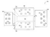
- FIG. 6illustrates a flow diagram of several methods according to various embodiments.
- the fuse link 102 , 202includes undoped polysilicon over shallow trench isolation (STI) oxide or local oxidation of silicon (LOCOS) oxide (not shown), the undoped polysilicon being under the silicide layer 210 .
- STIshallow trench isolation
- LOClocal oxidation of silicon
- FIG. 5illustrates a top view of an electrical fuse 500 with a heat sink according to various embodiments.
- the electrical fuse 500has many elements similar to the elements of the electrical fuses 100 , 200 , 400 shown in FIGS. 1 , 2 , and 4 , and similar elements in FIGS. 1 , 2 , 4 , and 5 have been given the same names.
- a fuse link 502is connected between an anode 504 and a cathode 506 .
- the fuse link 502is connected to the anode 504 by a tapered end 510 , and the fuse link 502 is connected to the cathode 506 by a rectangular connection 512 .
- the first heat sink 522has a plurality of contact plugs 526 connecting the first heat sink to an M1 plate or grid 530 to transfer heat away from the first heat sink 522 .
- the second heat sink 524has a plurality of contact plugs 532 connecting the second heat sink 524 to the M1 plate or grid 530 to transfer heat away from the second heat sink 524 .
- the M1 plate or grid 530is over the fuse link 502 , the tapered end 510 and the rectangular connection 512 .
- the M1 plate or grid 530is a blind or screen to be a security measure against an optical inspection of a programming state of the fuse link 502 , the anode 504 , and the cathode 506 .
- the highly doped polysilicon/silicide heat sinks 404 , 406 , 522 , 524are seated on thin gate oxide directly on top of a highly doped silicon substrate (not shown) to provide better heat transport to the silicon substrate.
- the contact plugs 424 , 426 , 526 , 532are located directly on a silicided and highly doped silicon substrate (not shown).
- Each silicide layer described hereinis selected from the group consisting of one or more of cobalt silicide, nickel silicide, platinum silicide, nickel platinum silicide, titanium silicide, tungsten silicide, ytterbium silicide, nickel ytterbium silicide, erbium silicide, and palladium silicide, in any combination according to various embodiments.
Landscapes
- Physics & Mathematics (AREA)
- Condensed Matter Physics & Semiconductors (AREA)
- General Physics & Mathematics (AREA)
- Engineering & Computer Science (AREA)
- Computer Hardware Design (AREA)
- Microelectronics & Electronic Packaging (AREA)
- Power Engineering (AREA)
- Design And Manufacture Of Integrated Circuits (AREA)
Abstract
Description
Claims (39)
Priority Applications (2)
| Application Number | Priority Date | Filing Date | Title |
|---|---|---|---|
| US11/670,770US7732898B2 (en) | 2007-02-02 | 2007-02-02 | Electrical fuse and associated methods |
| DE102008007234ADE102008007234A1 (en) | 2007-02-02 | 2008-02-01 | Electrical fuse and associated methods |
Applications Claiming Priority (1)
| Application Number | Priority Date | Filing Date | Title |
|---|---|---|---|
| US11/670,770US7732898B2 (en) | 2007-02-02 | 2007-02-02 | Electrical fuse and associated methods |
Publications (2)
| Publication Number | Publication Date |
|---|---|
| US20080186788A1 US20080186788A1 (en) | 2008-08-07 |
| US7732898B2true US7732898B2 (en) | 2010-06-08 |
Family
ID=39646230
Family Applications (1)
| Application Number | Title | Priority Date | Filing Date |
|---|---|---|---|
| US11/670,770Expired - Fee RelatedUS7732898B2 (en) | 2007-02-02 | 2007-02-02 | Electrical fuse and associated methods |
Country Status (2)
| Country | Link |
|---|---|
| US (1) | US7732898B2 (en) |
| DE (1) | DE102008007234A1 (en) |
Cited By (3)
| Publication number | Priority date | Publication date | Assignee | Title |
|---|---|---|---|---|
| US20080258256A1 (en)* | 2004-02-27 | 2008-10-23 | Nobuaki Otsuka | Semiconductor electrically programmable fuse element with amorphous silicon layer after programming and method of programming the same |
| US20120201010A1 (en)* | 2011-02-04 | 2012-08-09 | Murata Manufacturing Co., Ltd. | Electronic control device including interrupt wire |
| US12388015B2 (en) | 2022-11-10 | 2025-08-12 | Globalfoundries U.S. Inc. | E-fuse with metal fill |
Families Citing this family (20)
| Publication number | Priority date | Publication date | Assignee | Title |
|---|---|---|---|---|
| US7491585B2 (en) | 2006-10-19 | 2009-02-17 | International Business Machines Corporation | Electrical fuse and method of making |
| US7671444B2 (en)* | 2007-06-25 | 2010-03-02 | International Business Machines Corporation | Empty vias for electromigration during electronic-fuse re-programming |
| KR100856318B1 (en)* | 2007-06-25 | 2008-09-03 | 주식회사 동부하이텍 | Fuses for Semiconductor Devices |
| CN101170099B (en)* | 2007-11-30 | 2012-03-28 | 上海宏力半导体制造有限公司 | Multicrystalline silicon compounds electric fuse silk part |
| KR20090102555A (en)* | 2008-03-26 | 2009-09-30 | 삼성전자주식회사 | Electrical fuse device and methode of operating the same |
| US20090243032A1 (en)* | 2008-03-27 | 2009-10-01 | Shi-Bai Chen | Electrical fuse structure |
| US7642176B2 (en)* | 2008-04-21 | 2010-01-05 | Taiwan Semiconductor Manufacturing Company, Ltd. | Electrical fuse structure and method |
| JP5470633B2 (en)* | 2008-12-11 | 2014-04-16 | 国立大学法人東北大学 | Photoelectric conversion element and solar cell |
| US8026573B2 (en)* | 2008-12-15 | 2011-09-27 | United Microelectronics Corp. | Electrical fuse structure |
| US8102019B1 (en) | 2009-06-19 | 2012-01-24 | Xilinx, Inc. | Electrically programmable diffusion fuse |
| US8143695B1 (en) | 2009-07-24 | 2012-03-27 | Xilinx, Inc. | Contact fuse one time programmable memory |
| JP5224470B2 (en)* | 2009-07-31 | 2013-07-03 | 国立大学法人東北大学 | Photoelectric conversion member |
| DE102010045073B4 (en) | 2009-10-30 | 2021-04-22 | Taiwan Semiconductor Mfg. Co., Ltd. | Electrical fuse structure |
| US9741658B2 (en) | 2009-10-30 | 2017-08-22 | Taiwan Semiconductor Manufacturing Company, Ltd. | Electrical fuse structure and method of formation |
| US8686536B2 (en) | 2009-10-30 | 2014-04-01 | Taiwan Semiconductor Manufacturing Company, Ltd. | Electrical fuse structure and method of formation |
| DE102009055439A1 (en)* | 2009-12-31 | 2011-07-07 | GLOBALFOUNDRIES Dresden Module One Limited Liability Company & Co. KG, 01109 | Semiconductor device with semiconductor-based e-fuses with better programming efficiency through increased metal agglomeration and / or cavitation |
| KR101113187B1 (en)* | 2010-01-29 | 2012-02-15 | 주식회사 하이닉스반도체 | Semiconductor integrated circuit with electrical fuses to prevent thermal diffusion |
| US20120164799A1 (en)* | 2010-12-28 | 2012-06-28 | Globalfoundries Inc. | Method of Forming a Semiconductor Device Comprising eFuses of Increased Programming Window |
| US8896088B2 (en)* | 2011-04-27 | 2014-11-25 | International Business Machines Corporation | Reliable electrical fuse with localized programming |
| KR20150091895A (en)* | 2014-02-04 | 2015-08-12 | 에스케이하이닉스 주식회사 | Semiconductor device and method of operating the same |
Citations (34)
| Publication number | Priority date | Publication date | Assignee | Title |
|---|---|---|---|---|
| US5883000A (en)* | 1995-05-03 | 1999-03-16 | Lsi Logic Corporation | Circuit device interconnection by direct writing of patterns therein |
| US20020086462A1 (en) | 2000-12-28 | 2002-07-04 | Chandrasekharan Kothandaraman | Method and structure to reduce the damage associated with programming electrical fuses |
| US20020113291A1 (en) | 2001-02-16 | 2002-08-22 | International Business Machines Corporation | Fuse structure with thermal and crack-stop protection |
| US20030160297A1 (en) | 2002-02-28 | 2003-08-28 | Chandrasekharan Kothandaraman | System for programming fuse structure by electromigration of silicide enhanced by creating temperature gradient |
| US20030205777A1 (en) | 2002-04-04 | 2003-11-06 | Akira Ito | Integrated fuse with regions of different doping within the fuse neck |
| US20030211661A1 (en) | 1999-04-16 | 2003-11-13 | Marr Kenneth W. | Fuse for use in a semiconductor device, and semiconductor devices including the fuse |
| US20040038458A1 (en) | 2002-08-23 | 2004-02-26 | Marr Kenneth W. | Semiconductor fuses, semiconductor devices containing the same, and methods of making and using the same |
| US20040056325A1 (en) | 2001-08-03 | 2004-03-25 | Chandrasekharan Kothandaraman | Optically and electrically programmable silicided polysilicon fuse device |
| US20040099953A1 (en) | 2001-05-18 | 2004-05-27 | Taiwan Semiconductor Manufacturing Company | Redundancy structure in self-aligned contact process |
| US20040224444A1 (en) | 2003-01-09 | 2004-11-11 | Katsuhiro Hisaka | Fuse layout and method of trimming |
| US20050052892A1 (en)* | 2002-04-04 | 2005-03-10 | Broadcom Corporation | Systems for programmable memory using silicided poly-silicon fuses |
| US20050087836A1 (en) | 2003-10-22 | 2005-04-28 | Taiwan Semiconductor Manufacturing Co. | Electrically programmable polysilicon fuse with multiple level resistance and programming |
| US20050101114A1 (en) | 2002-03-11 | 2005-05-12 | Daubenspeck Timothy H. | Triple damascene fuse |
| US20050124097A1 (en) | 2003-12-05 | 2005-06-09 | Advanced Micro Devices, Inc | Integrated circuit with two phase fuse material and method of using and making same |
| US20050121741A1 (en) | 2003-12-03 | 2005-06-09 | Voldman Steven H. | Apparatus and method for electronic fuse with improved ESD tolerance |
| US6933591B1 (en)* | 2003-10-16 | 2005-08-23 | Altera Corporation | Electrically-programmable integrated circuit fuses and sensing circuits |
| US20050189613A1 (en)* | 2004-02-27 | 2005-09-01 | Nobuaki Otsuka | Semiconductor device as electrically programmable fuse element and method of programming the same |
| US20050221539A1 (en) | 1999-08-31 | 2005-10-06 | Samsung Electronics Co., Ltd. | Semiconductor device capable of preventing moisture-absorption of fuse area thereof and method for manufacturing the fuse area |
| US20050236688A1 (en) | 2004-04-21 | 2005-10-27 | Kwang-Kyu Bang | Fuse regions of a semiconductor memory device and methods of fabricating the same |
| US20050258506A1 (en) | 2003-10-02 | 2005-11-24 | Axel Brintzinger | Arrangement and process for protecting fuses/anti-fuses |
| US20050258990A1 (en)* | 2001-09-07 | 2005-11-24 | Babcock Jeffrey A | On chip heating for electrical trimming of polysilicon and polysilicon-silicon-germanium resistors and electrically programmable fuses for integrated circuits |
| US20050258505A1 (en) | 2004-05-20 | 2005-11-24 | Taiwan Semiconductor Manufacturing Co., Ltd. | Mixed implantation on polysilicon fuse for CMOS technology |
| US20050285222A1 (en) | 2004-06-29 | 2005-12-29 | Kong-Beng Thei | New fuse structure |
| US20060002187A1 (en) | 2001-02-13 | 2006-01-05 | Micron Technology, Inc. | Programmable fuse and antifuse and method therefor |
| US20060022300A1 (en) | 2004-08-02 | 2006-02-02 | Taiwan Semiconductor Manufacturing Co., Ltd | Self correcting multiple-link fuse |
| US20060030083A1 (en) | 2004-05-04 | 2006-02-09 | Bing-Chang Wu | Semiconductor device and fabricating method thereof |
| US20060081959A1 (en) | 2002-12-16 | 2006-04-20 | Koninklijke Philips Electronic N.V. | Poly-silicon stringer fuse |
| US20060087001A1 (en) | 2004-10-21 | 2006-04-27 | International Business Machines Corporation | Programmable semiconductor device |
| US20060108662A1 (en) | 2004-11-23 | 2006-05-25 | International Business Machines Corporation | An electrically programmable fuse for silicon-on-insulator (soi) technology |
| US20060157819A1 (en) | 2005-01-20 | 2006-07-20 | Bing-Chang Wu | Efuse structure |
| US20060189042A1 (en) | 2005-02-24 | 2006-08-24 | Nec Electronics Corporation | Semiconductor chip and method of fabricating the same |
| US20060208274A1 (en) | 2004-03-26 | 2006-09-21 | Chi-Hsi Wu | Electrical fuse for silicon-on-insulator devices |
| US20060223242A1 (en) | 2005-04-04 | 2006-10-05 | Daubenspeck Timothy H | Method of forming a crack stop void in a low-k dielectric layer between adjacent fusees |
| US20070252237A1 (en)* | 2006-04-26 | 2007-11-01 | Samsung Electronics Co., Ltd. | Devices and methods for constructing electrically programmable integrated fuses for low power applications |
- 2007
- 2007-02-02USUS11/670,770patent/US7732898B2/ennot_activeExpired - Fee Related
- 2008
- 2008-02-01DEDE102008007234Apatent/DE102008007234A1/ennot_activeCeased
Patent Citations (37)
| Publication number | Priority date | Publication date | Assignee | Title |
|---|---|---|---|---|
| US5883000A (en)* | 1995-05-03 | 1999-03-16 | Lsi Logic Corporation | Circuit device interconnection by direct writing of patterns therein |
| US20030211661A1 (en) | 1999-04-16 | 2003-11-13 | Marr Kenneth W. | Fuse for use in a semiconductor device, and semiconductor devices including the fuse |
| US20050221539A1 (en) | 1999-08-31 | 2005-10-06 | Samsung Electronics Co., Ltd. | Semiconductor device capable of preventing moisture-absorption of fuse area thereof and method for manufacturing the fuse area |
| US20020086462A1 (en) | 2000-12-28 | 2002-07-04 | Chandrasekharan Kothandaraman | Method and structure to reduce the damage associated with programming electrical fuses |
| US20060002187A1 (en) | 2001-02-13 | 2006-01-05 | Micron Technology, Inc. | Programmable fuse and antifuse and method therefor |
| US20020113291A1 (en) | 2001-02-16 | 2002-08-22 | International Business Machines Corporation | Fuse structure with thermal and crack-stop protection |
| US20040099953A1 (en) | 2001-05-18 | 2004-05-27 | Taiwan Semiconductor Manufacturing Company | Redundancy structure in self-aligned contact process |
| US20040056325A1 (en) | 2001-08-03 | 2004-03-25 | Chandrasekharan Kothandaraman | Optically and electrically programmable silicided polysilicon fuse device |
| US20050258990A1 (en)* | 2001-09-07 | 2005-11-24 | Babcock Jeffrey A | On chip heating for electrical trimming of polysilicon and polysilicon-silicon-germanium resistors and electrically programmable fuses for integrated circuits |
| US20030160297A1 (en) | 2002-02-28 | 2003-08-28 | Chandrasekharan Kothandaraman | System for programming fuse structure by electromigration of silicide enhanced by creating temperature gradient |
| US20050101114A1 (en) | 2002-03-11 | 2005-05-12 | Daubenspeck Timothy H. | Triple damascene fuse |
| US20030205777A1 (en) | 2002-04-04 | 2003-11-06 | Akira Ito | Integrated fuse with regions of different doping within the fuse neck |
| US20040222491A1 (en) | 2002-04-04 | 2004-11-11 | Broadcom Corporation | Integrated fuse with regions of different doping within the fuse neck |
| US20050052892A1 (en)* | 2002-04-04 | 2005-03-10 | Broadcom Corporation | Systems for programmable memory using silicided poly-silicon fuses |
| US20040038458A1 (en) | 2002-08-23 | 2004-02-26 | Marr Kenneth W. | Semiconductor fuses, semiconductor devices containing the same, and methods of making and using the same |
| US20050158919A1 (en) | 2002-08-23 | 2005-07-21 | Marr Kenneth W. | Semiconductor fuses and semiconductor devices containing the same |
| US20060081959A1 (en) | 2002-12-16 | 2006-04-20 | Koninklijke Philips Electronic N.V. | Poly-silicon stringer fuse |
| US20040224444A1 (en) | 2003-01-09 | 2004-11-11 | Katsuhiro Hisaka | Fuse layout and method of trimming |
| US20050258506A1 (en) | 2003-10-02 | 2005-11-24 | Axel Brintzinger | Arrangement and process for protecting fuses/anti-fuses |
| US6933591B1 (en)* | 2003-10-16 | 2005-08-23 | Altera Corporation | Electrically-programmable integrated circuit fuses and sensing circuits |
| US20050087836A1 (en) | 2003-10-22 | 2005-04-28 | Taiwan Semiconductor Manufacturing Co. | Electrically programmable polysilicon fuse with multiple level resistance and programming |
| US20060006494A1 (en) | 2003-10-22 | 2006-01-12 | Taiwan Semiconductor Manufacturing Co., Ltd. | Electrically programmable polysilicon fuse with multiple level resistance and programming |
| US20050121741A1 (en) | 2003-12-03 | 2005-06-09 | Voldman Steven H. | Apparatus and method for electronic fuse with improved ESD tolerance |
| US20050124097A1 (en) | 2003-12-05 | 2005-06-09 | Advanced Micro Devices, Inc | Integrated circuit with two phase fuse material and method of using and making same |
| US20050189613A1 (en)* | 2004-02-27 | 2005-09-01 | Nobuaki Otsuka | Semiconductor device as electrically programmable fuse element and method of programming the same |
| US20060208274A1 (en) | 2004-03-26 | 2006-09-21 | Chi-Hsi Wu | Electrical fuse for silicon-on-insulator devices |
| US20050236688A1 (en) | 2004-04-21 | 2005-10-27 | Kwang-Kyu Bang | Fuse regions of a semiconductor memory device and methods of fabricating the same |
| US20060030083A1 (en) | 2004-05-04 | 2006-02-09 | Bing-Chang Wu | Semiconductor device and fabricating method thereof |
| US20050258505A1 (en) | 2004-05-20 | 2005-11-24 | Taiwan Semiconductor Manufacturing Co., Ltd. | Mixed implantation on polysilicon fuse for CMOS technology |
| US20050285222A1 (en) | 2004-06-29 | 2005-12-29 | Kong-Beng Thei | New fuse structure |
| US20060022300A1 (en) | 2004-08-02 | 2006-02-02 | Taiwan Semiconductor Manufacturing Co., Ltd | Self correcting multiple-link fuse |
| US20060087001A1 (en) | 2004-10-21 | 2006-04-27 | International Business Machines Corporation | Programmable semiconductor device |
| US20060108662A1 (en) | 2004-11-23 | 2006-05-25 | International Business Machines Corporation | An electrically programmable fuse for silicon-on-insulator (soi) technology |
| US20060157819A1 (en) | 2005-01-20 | 2006-07-20 | Bing-Chang Wu | Efuse structure |
| US20060189042A1 (en) | 2005-02-24 | 2006-08-24 | Nec Electronics Corporation | Semiconductor chip and method of fabricating the same |
| US20060223242A1 (en) | 2005-04-04 | 2006-10-05 | Daubenspeck Timothy H | Method of forming a crack stop void in a low-k dielectric layer between adjacent fusees |
| US20070252237A1 (en)* | 2006-04-26 | 2007-11-01 | Samsung Electronics Co., Ltd. | Devices and methods for constructing electrically programmable integrated fuses for low power applications |
Cited By (7)
| Publication number | Priority date | Publication date | Assignee | Title |
|---|---|---|---|---|
| US20080258256A1 (en)* | 2004-02-27 | 2008-10-23 | Nobuaki Otsuka | Semiconductor electrically programmable fuse element with amorphous silicon layer after programming and method of programming the same |
| US8105886B2 (en)* | 2004-02-27 | 2012-01-31 | Kabushiki Kaisha Toshiba | Semiconductor electrically programmable fuse element with amorphous silicon layer after programming and method of programming the same |
| US20120201010A1 (en)* | 2011-02-04 | 2012-08-09 | Murata Manufacturing Co., Ltd. | Electronic control device including interrupt wire |
| US8971003B2 (en)* | 2011-02-04 | 2015-03-03 | Denso Corporation | Electronic control device including interrupt wire |
| US20150109746A1 (en)* | 2011-02-04 | 2015-04-23 | Denso Corporation | Electronic control device including interrupt wire |
| US9899178B2 (en)* | 2011-02-04 | 2018-02-20 | Denso Corporation | Electronic control device including interrupt wire |
| US12388015B2 (en) | 2022-11-10 | 2025-08-12 | Globalfoundries U.S. Inc. | E-fuse with metal fill |
Also Published As
| Publication number | Publication date |
|---|---|
| US20080186788A1 (en) | 2008-08-07 |
| DE102008007234A1 (en) | 2008-08-28 |
Similar Documents
| Publication | Publication Date | Title |
|---|---|---|
| US7732898B2 (en) | Electrical fuse and associated methods | |
| US7880266B2 (en) | Four-terminal antifuse structure having integrated heating elements for a programmable circuit | |
| KR100808997B1 (en) | Fuse and method disconnecting the fuse | |
| US7960808B2 (en) | Reprogrammable fuse structure and method | |
| US9355971B1 (en) | EOS protection for integrated circuits | |
| US20140167215A1 (en) | Electronic circuit arrangement | |
| US20060087001A1 (en) | Programmable semiconductor device | |
| US9059175B2 (en) | Forming BEOL line fuse structure | |
| WO2003073503A2 (en) | Fuse structure programming by electromigration of silicide enhanced by creating temperature gradient | |
| TW200913147A (en) | Electronic device and method for operating a memory circuit | |
| CN101562172A (en) | Semiconductor device with a plurality of semiconductor chips | |
| US7397106B2 (en) | Laser fuse with efficient heat dissipation | |
| US11355433B2 (en) | Semiconductor fuse structure and method of manufacturing a semiconductor fuse structure | |
| US7227207B2 (en) | Dense semiconductor fuse array | |
| CN104347589B (en) | A kind of anti-fuse structures | |
| US8421230B2 (en) | Microelectronic device provided with an array of elements made from a conductive polymer with a positive temperature coefficient | |
| CN118571293A (en) | Memory cell and method for managing the logical state of a memory cell | |
| JP2012527768A (en) | Electrically disconnected metal fuse structure for integrated circuits and method of forming the same | |
| Pedreira et al. | Reliability benchmark of various via prefill metals | |
| CN112599495A (en) | Semiconductor fuse structure and method for manufacturing the same | |
| CN110556380B (en) | Fuse unit, fuse bit cell structure and manufacturing method thereof | |
| US12119299B2 (en) | Semiconductor device and manufacturing method for the same | |
| Smedes et al. | ESD phenomena in interconnect structures | |
| JPS6059678B2 (en) | Programmable read-only memory device | |
| JP2006108584A (en) | Semiconductor device |
Legal Events
| Date | Code | Title | Description |
|---|---|---|---|
| AS | Assignment | Owner name:INFINEON TECHNOLOGIES AG, GERMANY Free format text:ASSIGNMENT OF ASSIGNORS INTEREST;ASSIGNOR:BARTH, HANS-JOACHIM;REEL/FRAME:018848/0131 Effective date:20070202 Owner name:INFINEON TECHNOLOGIES AG,GERMANY Free format text:ASSIGNMENT OF ASSIGNORS INTEREST;ASSIGNOR:BARTH, HANS-JOACHIM;REEL/FRAME:018848/0131 Effective date:20070202 | |
| FEPP | Fee payment procedure | Free format text:PAYOR NUMBER ASSIGNED (ORIGINAL EVENT CODE: ASPN); ENTITY STATUS OF PATENT OWNER: LARGE ENTITY | |
| STCF | Information on status: patent grant | Free format text:PATENTED CASE | |
| FPAY | Fee payment | Year of fee payment:4 | |
| MAFP | Maintenance fee payment | Free format text:PAYMENT OF MAINTENANCE FEE, 8TH YEAR, LARGE ENTITY (ORIGINAL EVENT CODE: M1552) Year of fee payment:8 | |
| FEPP | Fee payment procedure | Free format text:MAINTENANCE FEE REMINDER MAILED (ORIGINAL EVENT CODE: REM.); ENTITY STATUS OF PATENT OWNER: LARGE ENTITY | |
| LAPS | Lapse for failure to pay maintenance fees | Free format text:PATENT EXPIRED FOR FAILURE TO PAY MAINTENANCE FEES (ORIGINAL EVENT CODE: EXP.); ENTITY STATUS OF PATENT OWNER: LARGE ENTITY | |
| STCH | Information on status: patent discontinuation | Free format text:PATENT EXPIRED DUE TO NONPAYMENT OF MAINTENANCE FEES UNDER 37 CFR 1.362 | |
| FP | Lapsed due to failure to pay maintenance fee | Effective date:20220608 |