US7732876B2 - Power transistor with trench sinker for contacting the backside - Google Patents
Power transistor with trench sinker for contacting the backsideDownload PDFInfo
- Publication number
- US7732876B2 US7732876B2US12/038,184US3818408AUS7732876B2US 7732876 B2US7732876 B2US 7732876B2US 3818408 AUS3818408 AUS 3818408AUS 7732876 B2US7732876 B2US 7732876B2
- Authority
- US
- United States
- Prior art keywords
- gate
- trench
- sinker
- semiconductor region
- transistor
- Prior art date
- Legal status (The legal status is an assumption and is not a legal conclusion. Google has not performed a legal analysis and makes no representation as to the accuracy of the status listed.)
- Active, expires
Links
- 239000004065semiconductorSubstances0.000claimsabstractdescription39
- 239000004020conductorSubstances0.000claimsabstractdescription20
- 229910021420polycrystalline siliconInorganic materials0.000claimsdescription20
- 229920005591polysiliconPolymers0.000claimsdescription20
- 239000000758substrateSubstances0.000claimsdescription17
- 239000002184metalSubstances0.000claimsdescription14
- XUIMIQQOPSSXEZ-UHFFFAOYSA-NSiliconChemical compound[Si]XUIMIQQOPSSXEZ-UHFFFAOYSA-N0.000claimsdescription10
- 229910052710siliconInorganic materials0.000claimsdescription10
- 239000010703siliconSubstances0.000claimsdescription10
- 239000011810insulating materialSubstances0.000claimsdescription5
- 150000004767nitridesChemical class0.000claimsdescription5
- 229910052581Si3N4Inorganic materials0.000claimsdescription2
- 239000002019doping agentSubstances0.000claimsdescription2
- HQVNEWCFYHHQES-UHFFFAOYSA-Nsilicon nitrideChemical compoundN12[Si]34N5[Si]62N3[Si]51N64HQVNEWCFYHHQES-UHFFFAOYSA-N0.000claimsdescription2
- 229910000765intermetallicInorganic materials0.000claims1
- 238000000034methodMethods0.000description26
- 238000009792diffusion processMethods0.000description8
- 238000005530etchingMethods0.000description7
- 230000000694effectsEffects0.000description6
- 238000000206photolithographyMethods0.000description6
- VYPSYNLAJGMNEJ-UHFFFAOYSA-NSilicium dioxideChemical compoundO=[Si]=OVYPSYNLAJGMNEJ-UHFFFAOYSA-N0.000description4
- 238000004519manufacturing processMethods0.000description4
- 230000000873masking effectEffects0.000description4
- 230000008901benefitEffects0.000description3
- 230000015572biosynthetic processEffects0.000description3
- 238000007796conventional methodMethods0.000description3
- 238000011065in-situ storageMethods0.000description3
- 239000000463materialSubstances0.000description3
- 238000013459approachMethods0.000description2
- 230000000903blocking effectEffects0.000description2
- 238000012545processingMethods0.000description2
- 239000000377silicon dioxideSubstances0.000description2
- 229910020781SixOyInorganic materials0.000description1
- 150000001875compoundsChemical class0.000description1
- 238000005336crackingMethods0.000description1
- 230000001419dependent effectEffects0.000description1
- 230000009977dual effectEffects0.000description1
- 230000008030eliminationEffects0.000description1
- 238000003379elimination reactionMethods0.000description1
- 239000012212insulatorSubstances0.000description1
- 239000007769metal materialSubstances0.000description1
- 238000012856packingMethods0.000description1
- 235000012239silicon dioxideNutrition0.000description1
- 239000000126substanceSubstances0.000description1
- 238000012546transferMethods0.000description1
Images


Classifications
- H—ELECTRICITY
- H01—ELECTRIC ELEMENTS
- H01L—SEMICONDUCTOR DEVICES NOT COVERED BY CLASS H10
- H01L21/00—Processes or apparatus adapted for the manufacture or treatment of semiconductor or solid state devices or of parts thereof
- H01L21/70—Manufacture or treatment of devices consisting of a plurality of solid state components formed in or on a common substrate or of parts thereof; Manufacture of integrated circuit devices or of parts thereof
- H01L21/71—Manufacture of specific parts of devices defined in group H01L21/70
- H01L21/768—Applying interconnections to be used for carrying current between separate components within a device comprising conductors and dielectrics
- H—ELECTRICITY
- H01—ELECTRIC ELEMENTS
- H01L—SEMICONDUCTOR DEVICES NOT COVERED BY CLASS H10
- H01L21/00—Processes or apparatus adapted for the manufacture or treatment of semiconductor or solid state devices or of parts thereof
- H01L21/02—Manufacture or treatment of semiconductor devices or of parts thereof
- H01L21/04—Manufacture or treatment of semiconductor devices or of parts thereof the devices having potential barriers, e.g. a PN junction, depletion layer or carrier concentration layer
- H01L21/34—Manufacture or treatment of semiconductor devices or of parts thereof the devices having potential barriers, e.g. a PN junction, depletion layer or carrier concentration layer the devices having semiconductor bodies not provided for in groups H01L21/18, H10D48/04 and H10D48/07, with or without impurities, e.g. doping materials
- H01L21/46—Treatment of semiconductor bodies using processes or apparatus not provided for in groups H01L21/428
- H01L21/461—Treatment of semiconductor bodies using processes or apparatus not provided for in groups H01L21/428 to change their surface-physical characteristics or shape, e.g. etching, polishing, cutting
- H01L21/4763—Deposition of non-insulating, e.g. conductive -, resistive -, layers on insulating layers; After-treatment of these layers
- H—ELECTRICITY
- H10—SEMICONDUCTOR DEVICES; ELECTRIC SOLID-STATE DEVICES NOT OTHERWISE PROVIDED FOR
- H10D—INORGANIC ELECTRIC SEMICONDUCTOR DEVICES
- H10D30/00—Field-effect transistors [FET]
- H10D30/60—Insulated-gate field-effect transistors [IGFET]
- H10D30/64—Double-diffused metal-oxide semiconductor [DMOS] FETs
- H10D30/66—Vertical DMOS [VDMOS] FETs
- H10D30/663—Vertical DMOS [VDMOS] FETs having both source contacts and drain contacts on the same surface, i.e. up-drain VDMOS
- H—ELECTRICITY
- H10—SEMICONDUCTOR DEVICES; ELECTRIC SOLID-STATE DEVICES NOT OTHERWISE PROVIDED FOR
- H10D—INORGANIC ELECTRIC SEMICONDUCTOR DEVICES
- H10D30/00—Field-effect transistors [FET]
- H10D30/60—Insulated-gate field-effect transistors [IGFET]
- H10D30/64—Double-diffused metal-oxide semiconductor [DMOS] FETs
- H10D30/66—Vertical DMOS [VDMOS] FETs
- H10D30/665—Vertical DMOS [VDMOS] FETs having edge termination structures
- H—ELECTRICITY
- H10—SEMICONDUCTOR DEVICES; ELECTRIC SOLID-STATE DEVICES NOT OTHERWISE PROVIDED FOR
- H10D—INORGANIC ELECTRIC SEMICONDUCTOR DEVICES
- H10D30/00—Field-effect transistors [FET]
- H10D30/60—Insulated-gate field-effect transistors [IGFET]
- H10D30/64—Double-diffused metal-oxide semiconductor [DMOS] FETs
- H10D30/66—Vertical DMOS [VDMOS] FETs
- H10D30/668—Vertical DMOS [VDMOS] FETs having trench gate electrodes, e.g. UMOS transistors
- H—ELECTRICITY
- H10—SEMICONDUCTOR DEVICES; ELECTRIC SOLID-STATE DEVICES NOT OTHERWISE PROVIDED FOR
- H10D—INORGANIC ELECTRIC SEMICONDUCTOR DEVICES
- H10D62/00—Semiconductor bodies, or regions thereof, of devices having potential barriers
- H10D62/10—Shapes, relative sizes or dispositions of the regions of the semiconductor bodies; Shapes of the semiconductor bodies
- H10D62/113—Isolations within a component, i.e. internal isolations
- H10D62/115—Dielectric isolations, e.g. air gaps
- H10D62/116—Dielectric isolations, e.g. air gaps adjoining the input or output regions of field-effect devices, e.g. adjoining source or drain regions
- H—ELECTRICITY
- H10—SEMICONDUCTOR DEVICES; ELECTRIC SOLID-STATE DEVICES NOT OTHERWISE PROVIDED FOR
- H10D—INORGANIC ELECTRIC SEMICONDUCTOR DEVICES
- H10D64/00—Electrodes of devices having potential barriers
- H10D64/20—Electrodes characterised by their shapes, relative sizes or dispositions
- H10D64/23—Electrodes carrying the current to be rectified, amplified, oscillated or switched, e.g. sources, drains, anodes or cathodes
- H10D64/251—Source or drain electrodes for field-effect devices
- H10D64/252—Source or drain electrodes for field-effect devices for vertical or pseudo-vertical devices
- H—ELECTRICITY
- H10—SEMICONDUCTOR DEVICES; ELECTRIC SOLID-STATE DEVICES NOT OTHERWISE PROVIDED FOR
- H10D—INORGANIC ELECTRIC SEMICONDUCTOR DEVICES
- H10D64/00—Electrodes of devices having potential barriers
- H10D64/20—Electrodes characterised by their shapes, relative sizes or dispositions
- H10D64/23—Electrodes carrying the current to be rectified, amplified, oscillated or switched, e.g. sources, drains, anodes or cathodes
- H10D64/251—Source or drain electrodes for field-effect devices
- H10D64/256—Source or drain electrodes for field-effect devices for lateral devices wherein the source or drain electrodes are recessed in semiconductor bodies
- H—ELECTRICITY
- H01—ELECTRIC ELEMENTS
- H01L—SEMICONDUCTOR DEVICES NOT COVERED BY CLASS H10
- H01L2924/00—Indexing scheme for arrangements or methods for connecting or disconnecting semiconductor or solid-state bodies as covered by H01L24/00
- H01L2924/0001—Technical content checked by a classifier
- H01L2924/0002—Not covered by any one of groups H01L24/00, H01L24/00 and H01L2224/00
- H—ELECTRICITY
- H10—SEMICONDUCTOR DEVICES; ELECTRIC SOLID-STATE DEVICES NOT OTHERWISE PROVIDED FOR
- H10D—INORGANIC ELECTRIC SEMICONDUCTOR DEVICES
- H10D62/00—Semiconductor bodies, or regions thereof, of devices having potential barriers
- H10D62/10—Shapes, relative sizes or dispositions of the regions of the semiconductor bodies; Shapes of the semiconductor bodies
- H10D62/124—Shapes, relative sizes or dispositions of the regions of semiconductor bodies or of junctions between the regions
- H10D62/126—Top-view geometrical layouts of the regions or the junctions
- H10D62/127—Top-view geometrical layouts of the regions or the junctions of cellular field-effect devices, e.g. multicellular DMOS transistors or IGBTs
- H—ELECTRICITY
- H10—SEMICONDUCTOR DEVICES; ELECTRIC SOLID-STATE DEVICES NOT OTHERWISE PROVIDED FOR
- H10D—INORGANIC ELECTRIC SEMICONDUCTOR DEVICES
- H10D64/00—Electrodes of devices having potential barriers
- H10D64/20—Electrodes characterised by their shapes, relative sizes or dispositions
- H10D64/27—Electrodes not carrying the current to be rectified, amplified, oscillated or switched, e.g. gates
- H10D64/311—Gate electrodes for field-effect devices
- H10D64/411—Gate electrodes for field-effect devices for FETs
- H10D64/511—Gate electrodes for field-effect devices for FETs for IGFETs
- H10D64/514—Gate electrodes for field-effect devices for FETs for IGFETs characterised by the insulating layers
- H10D64/516—Gate electrodes for field-effect devices for FETs for IGFETs characterised by the insulating layers the thicknesses being non-uniform
Definitions
- This inventionrelates in general to semiconductor power devices and more particularly to power devices with top-side drain contact using a sinker trench.
- ICsintegrated circuits
- many power semiconductor deviceshave a vertical structure with the back of the die being an active electrical connection.
- the source and gate connectionsare at the top surface of the die and the drain connection is on the back side of the die.
- sinker trench structuresare used for this purpose.
- diffusion sinkersextending from the top-side of the die down to the substrate (which forms the drain contact region of the device) are used to make the drain contact available at the top surface of the die.
- a drawback of this techniqueis that the lateral diffusion during the formation of the diffusion sinkers results in consumption of a significant amount of the silicon area.
- metal-filled via extending from the top-side of the die clear through to the backside of the dieare used to bring the back-side contact to the top-side of the die.
- this techniquedoes not suffer from the loss of active area as in the diffusion sinker technique, it however requires formation of very deep via which adds to the complexity of the manufacturing process. Further, during conduction, the current is required to travel through long stretches of the substrate before reaching the drain contact, thus resulting in higher device on resistance Ron.
- a power transistorincludes a first semiconductor region of a first conductivity type extending over and in contact with a second semiconductor region of the first conductivity type.
- the first semiconductor regionhas a lower dopant concentration than the second semiconductor region.
- Gate trenchesextend into the first semiconductor region.
- Each gate trenchincludes a gate electrode and a gate dielectric layer lining gate trench sidewalls.
- Well regions of a second conductivity typeextend over and are in contact with the first semiconductor region. Each well region extends between and abuts every two adjacent gate trenches.
- a sinker trenchextends through the first semiconductor region and terminates within the second semiconductor region.
- the sinker trenchis laterally spaced from an outer one of the gate trenches, with no well regions abutting sidewalls of the sinker trench.
- Source regions of the first conductivity typeextend over and are in contact with the well regions, the source regions flanking the gate trenches.
- a conductive material in the sinker trenchmakes electrical contact with the second semiconductor region along the bottom of the sinker trench and makes electrical contact with a drain interconnect layer extending along the top of the sinker trench.
- the first semiconductor regionis an epitaxial layer and the second semiconductor region is a substrate.
- one of the well regionsextends between the outer one of the plurality of gate trenches and the sinker trench but does not abut the sinker trench.
- the conductive materialelectrically contacts the first semiconductor region along sidewalls of the sinker trench.
- the transistorincludes a sinker dielectric layer lining sidewalls of the sinker trench, and the sinker dielectric layer is thicker than the gate dielectric layer.
- each gate trenchincludes a shield electrode below the gate electrode, and the gate and shield electrodes are insulated from one another.
- a spacing between the sinker trench and the outer one of the plurality of gate trenchesis greater than a spacing between every two adjacent gate trenches.
- FIG. 1shows a simplified cross sectional view of an exemplary vertical power device in accordance with an embodiment of the invention
- FIGS. 2-4show various top layout views of a vertical power device with one or more sinker trenches in accordance with exemplary embodiments of the invention.
- FIG. 5is a top view illustrating the locations of interconnect balls in a ball-grid array package relative to a sinker trench extending along the perimeter of a die housed in the ball-grid array package, in accordance with an exemplary embodiment of the invention.
- a sinker trench terminating within the silicon substrateis filled with a highly conductive material such as doped polysilicon or metallic material.
- the sinker trenchis laterally spaced a predetermined distance from the active region wherein gate trenches are formed.
- the sinker trenchis wider and extends deeper than the gate trenches, and is lined with an insulator only along its sidewalls.
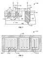
- FIG. 1shows a simplified cross sectional view of a vertical trenched-gate power MOSFET structure 100 in accordance with an exemplary embodiment of the invention.
- An n-type epitaxial layer 104extends over an n-type substrate 102 which forms the back side drain.
- a sinker trench 106extends from the top surface of epitaxial layer 104 through epitaxial layer 104 terminating within substrate 102 .
- a dielectric layer 110lines the sinker trench sidewalls.
- Dielectric layer 110may be from any one of oxide, silicon nitride, silicon oxynitride, multilayer of oxide and nitride, any known low k insulating material, and any known high k insulating material.
- Oxideas used in this disclosure means a chemical vapor deposited oxide (Si x O y ) or a thermally grown silicon dioxide (SiO 2 ).
- Sinker trench 106is filled with a conductive material 108 such as doped polysilicon, selective epitaxial silicon (SEG), metal, or metallic compounds.
- Conductive material 108is in electrical contact with substrate 102 along the bottom of sinker trench 106 .
- Conductive material 108thus makes the back-side drain available along the top side for interconnection. With the drain contact moved to the top surface, a back-side metal for contacting substrate 102 is no longer needed, but could be used in conjunction with the top side contact.
- the back side metal layermay be included for other purposes such as preventing the die from cracking and improving the heat transfer properties of the device.
- Gate trenches 112are laterally spaced from sinker trench 106 by a predetermined distance S 1 , and vertically extend from the top surface through p-type well regions 114 terminating at a predetermined depth within epitaxial layer 104 .
- Sinker trench 106is wider and deeper than gate trenches 112 .
- Gate trenches 112are lined with a dielectric layer 116 . The dielectric along the bottom of gate trenches 112 may optionally be made thicker than the dielectric along the gate trench sidewalls.
- Each gate trench 112includes a gate electrode 118 and a dielectric layer 120 atop gate electrode 118 to reduce the gate to drain capacitance.
- Source regions 122 of n-type conductivityextend along an upper portion of well regions 114 . Source regions 122 overlap gate electrodes 118 along the vertical dimension. As can be seen well region 114 terminates a distance away from sinker trench 106 . In one embodiment, this distance is dictated by the device blocking voltage rating. In another embodiment, well region 114 terminates at and thus abuts sinker trench 106 . In this embodiment, for higher blocking voltage ratings, the thickness of the dielectric layer along sinker trench sidewalls needs to be made larger since the sinker dielectric is required to withstand a higher voltage. This may require a wider sinker trench if the conductive material 108 is required to have a minimum width for current handling purposes.
- a conduction channel from source regions 122 to epitaxial layer 104is formed in well regions 114 along gate trench sidewalls.
- a currentthus flows from drain terminal 124 vertically through conductive material 108 of sinker trench 106 , then laterally through substrate 102 , and finally vertically through epitaxial layer 104 , the conduction channel in well regions 114 , and source regions 122 , to source terminal 126 .
- sinker trench 106 and gate trenches 114are formed at the same time. This is advantageous in that the sinker trench is self-aligned to the active region. In this embodiment, the widths of the sinker trench and the gate trenches and spacing S 1 between sinker trench 106 and the active region need to be carefully selected taking into account a number of factors.
- a ratio of width Ws of sinker trench 106 to width Wg of gate trenches 112needs to be selected so that upon completion of the trench etch step sinker trench 106 and gate trenches 112 terminate at the desired depths.
- the width ratio as well as spacing S 1needs to be carefully selected to minimize micro-loading effect which occurs when trenches with different features are simultaneously etched. Micro-loading effect, if not addressed properly, may cause trenches with a wide opening have a wider bottom than top. This can lead to such problems as formation of pin-holes in the conductive material in the sinker trench. The micro-loading effect can also be minimized by selecting proper etch material.
- the ratio of the width of the sinker trench to that of the gate trenchesis also dependent on the type of conductive material used in the sinker trench. In general, a ratio of the sinker trench width to the gate trench width of less than 10:1 is desirable. In one embodiment wherein doped polysilicon is used as the conductive material, a ratio of sinker trench width to gate trench width of less than 5:1 is desirable. For example, for a gate trench width of 0.5 ⁇ m, a sinker trench width in the range of about 0.7 ⁇ m to 2.5 ⁇ m would be selected. If a metal or other highly conductive material is used in the sinker trench, a higher ratio (e.g., 3:1) is more desirable. Other than the relative width of the trenches, spacing S 1 between the sinker trench and the active region also impacts the micro-loading effect. A smaller spacing generally results in reduced micro-loading effect.
- the depth of the gate trenches in the epitaxial layeris selected to be close to the interface between substrate 102 and epitaxial layer 104 so that a slightly wider sinker trench would reach through to contact substrate 102 .
- both the gate trenches and the sinker trenchterminate within substrate 102 .
- the sinker trench and the gate trenchesare formed at different times. Thought the sinker trench would not be self-aligned to the active region, spacing S 1 is not a critical dimension. Advantages of forming the two trenches at different times include elimination of the micro-loading effect, and the ability to optimize each trench separately.
- a method of forming the power transistor shown in FIG. 1 wherein the sinker trench and gate trenches are formed simultaneouslyis as follows.
- Epitaxial layer 104is formed over substrate 102 .
- a masking layeris used to pattern the gate trench and sinker trench openings.
- Conventional plasma etch techniquesare used to etch the silicon to form the sinker trench and gate trenches.
- An insulating layer, e.g., oxide,is then formed along sidewalls and bottom of both the gate trenches and the sinker trench.
- Increasing the insulating thickness or increase in the dielectric constant of the insulating materialis advantageous in minimizing the area between the depletion region and sinker trench, distance S 1 , as some of the voltage from the depletion layer will be supported by the insulating layer thus reducing consumed silicon area by use of a sinker trench.
- a nitride layeris formed over the oxide layer in all trenches.
- the oxide and nitride layersare then removed from the bottom of the sinker trench using conventional photolithography and anisotropic etch techniques thus leaving an oxide-nitride bi-layer along the sinker trench sidewalls.
- anisotropic and isotropic etching or isotropic etching alonecan be used.
- the combination of anisotropic and isotropic etchingcan advantageously be used to respectively remove the nitride and oxide layers from lower sidewall portions of the trench sinker (e.g., those lower sidewall portions extending in the substrate or even in the epitaxial layer—this would advantageously reduce the on-resistance).
- the resulting thicker bi-layer of dielectric along sinker trench sidewallsis advantageously capable of withstanding higher drain voltages.
- the sinker trench and gate trenchesare then filled with in-situ doped polysilicon.
- the doped polysiliconis then etched back to planarize the top of the polysilicon in the trenches with the top surface of epitaxial layer 104 .
- the polysilicon and oxide-nitride bi-layerare removed from the gate trenches.
- the gate trenchesare then lined with a gate oxide layer and filled with gate polysilicon material.
- the excess gate polysilicon over the sinker trenchis removed using a conventional photolithography and etch process to pattern the gate electrode.
- the remaining process steps for forming the insulating layer over the gate electrodes, the well regions, the source regions, the source and drain metal contact layers, as well as other steps to complete the deviceare carried out in accordance with conventional methods.
- a thick oxide layer(as mentioned above, to reduce the spacing of the sinker trench to the well region) is formed along the sidewalls and bottom of the gate and sinker trenches.
- the thick oxide layeris then removed from the bottom of the sinker trenches using conventional photolithography and anisotropic etch techniques thus leaving the sidewalls of the sinker trench lined with the thick oxide while the gate trenches are protected.
- anisotropic and isotropic etchingcan be used to also remove the thick oxide from lower portions of the trench sinker sidewalls.
- the oxide layermay act as a sacrificial insulating layer for the gate trenches to improve the gate oxide integrity.
- the sinker trench and gate trenchesare then filled with in-situ doped polysilicon.
- the doped polysiliconis then etched back to planarize the top of the polysilicon in the trenches with the top surface of epitaxial layer 104 .
- the polysilicon and insulating layerare removed from the gate trenches.
- the gate trenchesare then lined with a gate insulating layer and filled with gate polysilicon material.
- the excess gate polysilicon over the sinker trenchesis removed using a conventional photolithography and etch process to pattern the gate electrode.
- the remaining process steps for forming the insulating layer over the gate electrodes, the well regions, the source regions, the source and drain metal contact layers, as well as other steps to complete the deviceare carried out in accordance with conventional methods.
- an insulating layere.g., gate oxide
- the gate oxide layeris then removed from the bottom of the sinker trenches using conventional photolithography and anisotropic etch techniques thus leaving an oxide layer lining the sidewalls of the sinker trench while the gate trenches are protected.
- anisotropic and isotropic etching or isotropic etching alonecan be used.
- the combination of anisotropic and isotropic etchingcan advantageously be used to remove the gate oxide layer from lower sidewall portions of the trench sinker (e.g., those lower sidewall portions extending in the substrate or even in the epitaxial layer—this would advantageously reduce the on-resistance).
- the sinker trench and gate trenchesare then filled with in-situ doped polysilicon.
- the doped polysiliconis then patterned using conventional photolithography techniques and etched to form both the sinker (drain) and gate electrodes.
- the remaining process steps for forming the insulating layer over the gate electrodes, the well regions, the source regions, the source and drain metal contact layers, as well as other steps to complete the deviceare carried out in accordance with conventional methods.
- the sinker trench and gate trenchesare formed independently by using separate masking steps. For example, using a first set of masks and processing steps the gate trenches are defined and etched, lined with gate oxide, and filled with polysilicon. Using a second set of masks and processing steps the sinker trench is defined and etched, lined with dielectric layer along its sidewalls, and filled with a conductive material. The order in which the sinker trench and gate trenches are formed may be reversed.
- FIG. 2shows a simplified top layout view of the power device with sinker trench in accordance with an exemplary embodiment of the invention.
- the FIG. 2 layout viewdepicts a stripe-shaped cell configuration.
- Stripe-shaped gate trenches 212 aextend vertically and terminate in horizontally-extending gate trenches 212 b .
- the three groups of striped gate trenchesare surrounded by a contiguous sinker trench 206 .
- sinker trenches 306are disposed between groups of gate trenches (only two of which are shown) and are repeated at such frequency and spacing as dictated by the desired Ron.
- the spacing between adjacent sinker trenchesneeds to be two times the thickness of the wafer. For example, for a 4 mils thick wafer, the sinker trenches may be spaced from one another by approximately 8 mils. For even a lower Ron, the sinker trenches may be placed closer together.
- striped gate trenches 412extend horizontally, and vertically extending sinker trenches 406 separate the different groups of gate trenches. Sinker trenches 406 are interconnected by a metal interconnect 432 . Metal interconnect is shown as being enlarged along the right side of the figure forming a drain pad for bond-wire connection. Also a gate pad 430 is shown in a cut-out corner of one of the groups of gate trenches.
- FIG. 5shows a top view of a die housing the power device with sinker trenches in accordance with an embodiment of the invention.
- the small circlesdepict the balls of a ball grid array package.
- the outer perimeter region 506includes the sinker trench, and the balls in outer periphery region 506 thus provide the drain connection.
- Central region 507represents the active region and the balls inside this region provide the source connection.
- the small square region 530 at the bottom left corner of central region 508represents the gate pad and the ball inside region 530 provides the gate connection.
- the sinker trench structure 106 in FIG. 1may be used to bring the backside connection of any power device to the top surface and as such is not limited to use with vertical trenched-gate power MOSFETs.
- Same or similar sinker trench structuresmay be similarly integrated with such other vertically conducting power devices as planar gate MOSFETs (i.e., MOSFETs with the gate and its underlying channel region extending over and parallel to the silicon surface), and power diodes to make the anode or cathode contact regions available along the top for interconnection.
- planar gate MOSFETsi.e., MOSFETs with the gate and its underlying channel region extending over and parallel to the silicon surface
- power diodesto make the anode or cathode contact regions available along the top for interconnection.
- Many other variations and alternativesare possible, including use of shielded gate and dual gate structures in different combinations with various charge balancing techniques many of which are described in detail in the above-referenced commonly assigned patent application Ser. No.
- FIGS. 2-5show layout implementations based on the open cell configuration, the invention is not limited as such.
- the structure shown in FIG. 1can also be implemented in any one of a number of well known closed cell configurations.
- the dimensions in the cross section view in FIG. 1 and the top layout views in FIGS. 2-5are not to scale and are merely illustrative.
Landscapes
- Engineering & Computer Science (AREA)
- Physics & Mathematics (AREA)
- Condensed Matter Physics & Semiconductors (AREA)
- General Physics & Mathematics (AREA)
- Manufacturing & Machinery (AREA)
- Computer Hardware Design (AREA)
- Microelectronics & Electronic Packaging (AREA)
- Power Engineering (AREA)
- Electrodes Of Semiconductors (AREA)
- Insulated Gate Type Field-Effect Transistor (AREA)
- Internal Circuitry In Semiconductor Integrated Circuit Devices (AREA)
Abstract
Description
Claims (20)
Priority Applications (4)
| Application Number | Priority Date | Filing Date | Title |
|---|---|---|---|
| US12/038,184US7732876B2 (en) | 2004-08-03 | 2008-02-27 | Power transistor with trench sinker for contacting the backside |
| US12/794,936US8026558B2 (en) | 2004-08-03 | 2010-06-07 | Semiconductor power device having a top-side drain using a sinker trench |
| US13/178,391US8148233B2 (en) | 2004-08-03 | 2011-07-07 | Semiconductor power device having a top-side drain using a sinker trench |
| US13/347,496US20120153384A1 (en) | 2004-08-03 | 2012-01-10 | Semiconductor Power Device Having A Top-side Drain Using A Sinker Trench |
Applications Claiming Priority (3)
| Application Number | Priority Date | Filing Date | Title |
|---|---|---|---|
| US59867804P | 2004-08-03 | 2004-08-03 | |
| US11/194,060US7352036B2 (en) | 2004-08-03 | 2005-07-28 | Semiconductor power device having a top-side drain using a sinker trench |
| US12/038,184US7732876B2 (en) | 2004-08-03 | 2008-02-27 | Power transistor with trench sinker for contacting the backside |
Related Parent Applications (1)
| Application Number | Title | Priority Date | Filing Date |
|---|---|---|---|
| US11/194,060ContinuationUS7352036B2 (en) | 2004-08-03 | 2005-07-28 | Semiconductor power device having a top-side drain using a sinker trench |
Related Child Applications (1)
| Application Number | Title | Priority Date | Filing Date |
|---|---|---|---|
| US12/794,936DivisionUS8026558B2 (en) | 2004-08-03 | 2010-06-07 | Semiconductor power device having a top-side drain using a sinker trench |
Publications (2)
| Publication Number | Publication Date |
|---|---|
| US20080142883A1 US20080142883A1 (en) | 2008-06-19 |
| US7732876B2true US7732876B2 (en) | 2010-06-08 |
Family
ID=35839819
Family Applications (5)
| Application Number | Title | Priority Date | Filing Date |
|---|---|---|---|
| US11/194,060Expired - LifetimeUS7352036B2 (en) | 2004-08-03 | 2005-07-28 | Semiconductor power device having a top-side drain using a sinker trench |
| US12/038,184Active2026-03-06US7732876B2 (en) | 2004-08-03 | 2008-02-27 | Power transistor with trench sinker for contacting the backside |
| US12/794,936Expired - LifetimeUS8026558B2 (en) | 2004-08-03 | 2010-06-07 | Semiconductor power device having a top-side drain using a sinker trench |
| US13/178,391Expired - LifetimeUS8148233B2 (en) | 2004-08-03 | 2011-07-07 | Semiconductor power device having a top-side drain using a sinker trench |
| US13/347,496AbandonedUS20120153384A1 (en) | 2004-08-03 | 2012-01-10 | Semiconductor Power Device Having A Top-side Drain Using A Sinker Trench |
Family Applications Before (1)
| Application Number | Title | Priority Date | Filing Date |
|---|---|---|---|
| US11/194,060Expired - LifetimeUS7352036B2 (en) | 2004-08-03 | 2005-07-28 | Semiconductor power device having a top-side drain using a sinker trench |
Family Applications After (3)
| Application Number | Title | Priority Date | Filing Date |
|---|---|---|---|
| US12/794,936Expired - LifetimeUS8026558B2 (en) | 2004-08-03 | 2010-06-07 | Semiconductor power device having a top-side drain using a sinker trench |
| US13/178,391Expired - LifetimeUS8148233B2 (en) | 2004-08-03 | 2011-07-07 | Semiconductor power device having a top-side drain using a sinker trench |
| US13/347,496AbandonedUS20120153384A1 (en) | 2004-08-03 | 2012-01-10 | Semiconductor Power Device Having A Top-side Drain Using A Sinker Trench |
Country Status (8)
| Country | Link |
|---|---|
| US (5) | US7352036B2 (en) |
| JP (1) | JP2008509557A (en) |
| KR (1) | KR100848968B1 (en) |
| CN (1) | CN100576466C (en) |
| AT (1) | AT502860A2 (en) |
| DE (1) | DE112005001675B4 (en) |
| TW (1) | TWI389309B (en) |
| WO (1) | WO2006017376A2 (en) |
Cited By (3)
| Publication number | Priority date | Publication date | Assignee | Title |
|---|---|---|---|---|
| US20080258214A1 (en)* | 2007-04-17 | 2008-10-23 | Byung Tak Jang | Semiconductor Device and Method of Fabricating the Same |
| US20110163374A1 (en)* | 2010-01-06 | 2011-07-07 | Ptek Technology Co., Ltd. | Trench-typed power mos transistor and method for making the same |
| US20110198689A1 (en)* | 2010-02-17 | 2011-08-18 | Suku Kim | Semiconductor devices containing trench mosfets with superjunctions |
Families Citing this family (77)
| Publication number | Priority date | Publication date | Assignee | Title |
|---|---|---|---|---|
| US6004835A (en)* | 1997-04-25 | 1999-12-21 | Micron Technology, Inc. | Method of forming integrated circuitry, conductive lines, a conductive grid, a conductive network, an electrical interconnection to anode location and an electrical interconnection with a transistor source/drain region |
| US7352036B2 (en) | 2004-08-03 | 2008-04-01 | Fairchild Semiconductor Corporation | Semiconductor power device having a top-side drain using a sinker trench |
| US7535057B2 (en)* | 2005-05-24 | 2009-05-19 | Robert Kuo-Chang Yang | DMOS transistor with a poly-filled deep trench for improved performance |
| KR101296984B1 (en) | 2005-06-10 | 2013-08-14 | 페어차일드 세미컨덕터 코포레이션 | Charge balance field effect transistor |
| US7868394B2 (en)* | 2005-08-09 | 2011-01-11 | United Microelectronics Corp. | Metal-oxide-semiconductor transistor and method of manufacturing the same |
| JP2007142272A (en)* | 2005-11-21 | 2007-06-07 | Sanyo Electric Co Ltd | Semiconductor device |
| JP2008060537A (en)* | 2006-07-31 | 2008-03-13 | Sanyo Electric Co Ltd | Semiconductor device and manufacturing method thereof |
| US7579650B2 (en)* | 2006-08-09 | 2009-08-25 | International Rectifier Corporation | Termination design for deep source electrode MOSFET |
| US7468536B2 (en)* | 2007-02-16 | 2008-12-23 | Power Integrations, Inc. | Gate metal routing for transistor with checkerboarded layout |
| JP2008251923A (en)* | 2007-03-30 | 2008-10-16 | Sanyo Electric Co Ltd | Semiconductor device |
| US7884390B2 (en)* | 2007-10-02 | 2011-02-08 | Fairchild Semiconductor Corporation | Structure and method of forming a topside contact to a backside terminal of a semiconductor device |
| US7550803B1 (en)* | 2008-04-15 | 2009-06-23 | United Microelectronics Corp. | Vertical double-diffusion metal-oxide-semiconductor transistor device |
| TWI384623B (en)* | 2008-04-16 | 2013-02-01 | United Microelectronics Corp | Vertical double-diffusion metal-oxide-semiconductor transistor device |
| US7781832B2 (en)* | 2008-05-28 | 2010-08-24 | Ptek Technology Co., Ltd. | Trench-type power MOS transistor and integrated circuit utilizing the same |
| US7807576B2 (en)* | 2008-06-20 | 2010-10-05 | Fairchild Semiconductor Corporation | Structure and method for forming a thick bottom dielectric (TBD) for trench-gate devices |
| US7943449B2 (en)* | 2008-09-30 | 2011-05-17 | Infineon Technologies Austria Ag | Semiconductor component structure with vertical dielectric layers |
| KR101009399B1 (en)* | 2008-10-01 | 2011-01-19 | 주식회사 동부하이텍 | LDMOS transistors and methods of manufacturing the same |
| US8304829B2 (en) | 2008-12-08 | 2012-11-06 | Fairchild Semiconductor Corporation | Trench-based power semiconductor devices with increased breakdown voltage characteristics |
| US8174067B2 (en)* | 2008-12-08 | 2012-05-08 | Fairchild Semiconductor Corporation | Trench-based power semiconductor devices with increased breakdown voltage characteristics |
| US8298889B2 (en) | 2008-12-10 | 2012-10-30 | Semiconductor Components Industries, Llc | Process of forming an electronic device including a trench and a conductive structure therein |
| US8227855B2 (en)* | 2009-02-09 | 2012-07-24 | Fairchild Semiconductor Corporation | Semiconductor devices with stable and controlled avalanche characteristics and methods of fabricating the same |
| US8148749B2 (en)* | 2009-02-19 | 2012-04-03 | Fairchild Semiconductor Corporation | Trench-shielded semiconductor device |
| US8049276B2 (en) | 2009-06-12 | 2011-11-01 | Fairchild Semiconductor Corporation | Reduced process sensitivity of electrode-semiconductor rectifiers |
| WO2011027831A1 (en) | 2009-09-07 | 2011-03-10 | ローム株式会社 | Semiconductor device and process for production thereof |
| JP5638218B2 (en)* | 2009-10-15 | 2014-12-10 | 三菱電機株式会社 | Semiconductor device and manufacturing method thereof |
| DE102009049671B4 (en)* | 2009-10-16 | 2020-02-27 | Infineon Technologies Ag | Integrated circuit with ESD structure |
| EP2317553B1 (en)* | 2009-10-28 | 2012-12-26 | STMicroelectronics Srl | Double-sided semiconductor structure and method for manufacturing the same |
| US9306056B2 (en) | 2009-10-30 | 2016-04-05 | Vishay-Siliconix | Semiconductor device with trench-like feed-throughs |
| US8604525B2 (en) | 2009-11-02 | 2013-12-10 | Vishay-Siliconix | Transistor structure with feed-through source-to-substrate contact |
| US8519473B2 (en)* | 2010-07-14 | 2013-08-27 | Infineon Technologies Ag | Vertical transistor component |
| US8304825B2 (en)* | 2010-09-22 | 2012-11-06 | Monolithic Power Systems, Inc. | Vertical discrete devices with trench contacts and associated methods of manufacturing |
| US8598654B2 (en) | 2011-03-16 | 2013-12-03 | Fairchild Semiconductor Corporation | MOSFET device with thick trench bottom oxide |
| JP5641995B2 (en)* | 2011-03-23 | 2014-12-17 | 株式会社東芝 | Semiconductor element |
| US8487371B2 (en)* | 2011-03-29 | 2013-07-16 | Fairchild Semiconductor Corporation | Vertical MOSFET transistor having source/drain contacts disposed on the same side and method for manufacturing the same |
| JP5881322B2 (en)* | 2011-04-06 | 2016-03-09 | ローム株式会社 | Semiconductor device |
| US9159828B2 (en)* | 2011-04-27 | 2015-10-13 | Alpha And Omega Semiconductor Incorporated | Top drain LDMOS |
| CN102832244B (en)* | 2011-06-13 | 2015-08-26 | 万国半导体股份有限公司 | Semiconductor device with device terminal electrode with exposed substrate terminal and method for manufacturing the same |
| JP2013030618A (en) | 2011-07-28 | 2013-02-07 | Rohm Co Ltd | Semiconductor device |
| US9059329B2 (en)* | 2011-08-22 | 2015-06-16 | Monolithic Power Systems, Inc. | Power device with integrated Schottky diode and method for making the same |
| US8604542B2 (en)* | 2011-08-23 | 2013-12-10 | Nan Ya Technology Corporation | Circuit structure with conductive and depletion regions to form tunable capacitors and resistors |
| US8836029B2 (en)* | 2012-02-29 | 2014-09-16 | Smsc Holdings S.A.R.L. | Transistor with minimized resistance |
| KR20130119193A (en)* | 2012-04-23 | 2013-10-31 | 주식회사 동부하이텍 | Backside illumination image sensor and method for fabricating the same |
| US8823096B2 (en)* | 2012-06-01 | 2014-09-02 | Taiwan Semiconductor Manufacturing Company, Ltd. | Vertical power MOSFET and methods for forming the same |
| US9130060B2 (en) | 2012-07-11 | 2015-09-08 | Taiwan Semiconductor Manufacturing Company, Ltd. | Integrated circuit having a vertical power MOS transistor |
| US8669611B2 (en) | 2012-07-11 | 2014-03-11 | Taiwan Semiconductor Manufacturing Company, Ltd. | Apparatus and method for power MOS transistor |
| CN103928513B (en)* | 2013-01-15 | 2017-03-29 | 无锡华润上华半导体有限公司 | A kind of trench-dmos devices and preparation method thereof |
| US8999783B2 (en)* | 2013-02-06 | 2015-04-07 | Infineon Technologies Austria Ag | Method for producing a semiconductor device with a vertical dielectric layer |
| US9159652B2 (en) | 2013-02-25 | 2015-10-13 | Stmicroelectronics S.R.L. | Electronic device comprising at least a chip enclosed in a package and a corresponding assembly process |
| CN104218078B (en)* | 2013-06-05 | 2017-11-07 | 帅群微电子股份有限公司 | Power transistor with drain on top and method of forming the same |
| US9559198B2 (en)* | 2013-08-27 | 2017-01-31 | Nxp Usa, Inc. | Semiconductor device and method of manufacture therefor |
| US20170186866A1 (en)* | 2014-03-20 | 2017-06-29 | Skokie Swift Corporation | Vertical field effect transistor having a disc shaped gate |
| US9425304B2 (en) | 2014-08-21 | 2016-08-23 | Vishay-Siliconix | Transistor structure with improved unclamped inductive switching immunity |
| JP2016062967A (en)* | 2014-09-16 | 2016-04-25 | 株式会社東芝 | Semiconductor device and method of manufacturing the same |
| US9837526B2 (en) | 2014-12-08 | 2017-12-05 | Nxp Usa, Inc. | Semiconductor device wtih an interconnecting semiconductor electrode between first and second semiconductor electrodes and method of manufacture therefor |
| US9691751B2 (en)* | 2014-12-15 | 2017-06-27 | Texas Instruments Incorporated | In-situ doped polysilicon filler for trenches |
| US9559158B2 (en) | 2015-01-12 | 2017-01-31 | The Hong Kong University Of Science And Technology | Method and apparatus for an integrated capacitor |
| US20160247879A1 (en)* | 2015-02-23 | 2016-08-25 | Polar Semiconductor, Llc | Trench semiconductor device layout configurations |
| DE102015108091A1 (en)* | 2015-05-21 | 2016-11-24 | Infineon Technologies Dresden Gmbh | Transistor arrangement with power transistors and voltage-limiting components |
| US10348295B2 (en) | 2015-11-19 | 2019-07-09 | Nxp Usa, Inc. | Packaged unidirectional power transistor and control circuit therefore |
| CN105938849A (en)* | 2016-02-03 | 2016-09-14 | 杭州立昂微电子股份有限公司 | Manufacturing method for Schottky chip used for chip scale packaging |
| CN105938848A (en)* | 2016-02-03 | 2016-09-14 | 杭州立昂微电子股份有限公司 | Schottky chip used for chip scale packaging |
| CN105826288B (en)* | 2016-03-22 | 2019-08-13 | 上海朕芯微电子科技有限公司 | The CSP encapsulating structure and its manufacturing method of power device |
| DE102016107203B4 (en) | 2016-04-19 | 2021-12-23 | Infineon Technologies Austria Ag | Power semiconductor device trench with field plate and gate electrode and method for production |
| CN105845735A (en)* | 2016-04-28 | 2016-08-10 | 上海格瑞宝电子有限公司 | MOSFET and preparation method thereof |
| CN105762193A (en)* | 2016-04-28 | 2016-07-13 | 上海格瑞宝电子有限公司 | MOSFET and preparation method thereof |
| JP6923303B2 (en)* | 2016-10-20 | 2021-08-18 | ローム株式会社 | Diode element |
| JP2019046991A (en)* | 2017-09-04 | 2019-03-22 | ルネサスエレクトロニクス株式会社 | Semiconductor device and method of manufacturing the same |
| EP3474318A1 (en)* | 2017-10-23 | 2019-04-24 | Nexperia B.V. | Semiconductor device and method of manufacture |
| CN107978632B (en)* | 2017-11-30 | 2020-06-16 | 电子科技大学 | Multi-channel transverse high-voltage device |
| CN110620143A (en)* | 2018-06-20 | 2019-12-27 | 夏令 | Mixed channel compound semiconductor device |
| US11031281B2 (en)* | 2019-06-04 | 2021-06-08 | Globalfoundries Singapore Pte. Ltd. | Semiconductor devices and methods of fabricating a deep trench isolation structure |
| JP7495257B2 (en)* | 2020-03-24 | 2024-06-04 | 株式会社東海理化電機製作所 | Semiconductor integrated circuit and manufacturing method thereof |
| KR102374125B1 (en) | 2020-08-20 | 2022-03-11 | 주식회사 키파운드리 | Semiconductor Device having Vertical DMOS and Manufacturing Method Thereof |
| US11670693B2 (en) | 2021-01-28 | 2023-06-06 | Semiconductor Components Industries, Llc | Trench gate field-effect transistors with drain runner |
| JP7631083B2 (en)* | 2021-04-30 | 2025-02-18 | 株式会社豊田中央研究所 | Semiconductor Device |
| CN119521785A (en)* | 2023-08-15 | 2025-02-25 | 艾科微电子(深圳)有限公司 | Semiconductor components |
| CN116978954A (en)* | 2023-09-25 | 2023-10-31 | 深圳天狼芯半导体有限公司 | Groove type MOSFET device and manufacturing method |
Citations (362)
| Publication number | Priority date | Publication date | Assignee | Title |
|---|---|---|---|---|
| US3404295A (en) | 1964-11-30 | 1968-10-01 | Motorola Inc | High frequency and voltage transistor with added region for punch-through protection |
| US3412297A (en) | 1965-12-16 | 1968-11-19 | United Aircraft Corp | Mos field-effect transistor with a onemicron vertical channel |
| US3497777A (en) | 1967-06-13 | 1970-02-24 | Stanislas Teszner | Multichannel field-effect semi-conductor device |
| US3564356A (en) | 1968-10-24 | 1971-02-16 | Tektronix Inc | High voltage integrated circuit transistor |
| US3660697A (en) | 1970-02-16 | 1972-05-02 | Bell Telephone Labor Inc | Monolithic semiconductor apparatus adapted for sequential charge transfer |
| US4003072A (en) | 1972-04-20 | 1977-01-11 | Sony Corporation | Semiconductor device with high voltage breakdown resistance |
| US4011105A (en) | 1975-09-15 | 1977-03-08 | Mos Technology, Inc. | Field inversion control for n-channel device integrated circuits |
| US4300150A (en) | 1980-06-16 | 1981-11-10 | North American Philips Corporation | Lateral double-diffused MOS transistor device |
| US4324038A (en) | 1980-11-24 | 1982-04-13 | Bell Telephone Laboratories, Incorporated | Method of fabricating MOS field effect transistors |
| US4326332A (en) | 1980-07-28 | 1982-04-27 | International Business Machines Corp. | Method of making a high density V-MOS memory array |
| US4337474A (en) | 1978-08-31 | 1982-06-29 | Mitsubishi Denki Kabushiki Kaisha | Semiconductor device |
| US4338616A (en) | 1980-02-19 | 1982-07-06 | Xerox Corporation | Self-aligned Schottky metal semi-conductor field effect transistor with buried source and drain |
| US4345265A (en) | 1980-04-14 | 1982-08-17 | Supertex, Inc. | MOS Power transistor with improved high-voltage capability |
| US4445202A (en) | 1980-11-12 | 1984-04-24 | International Business Machines Corporation | Electrically switchable permanent storage |
| US4568958A (en) | 1984-01-03 | 1986-02-04 | General Electric Company | Inversion-mode insulated-gate gallium arsenide field-effect transistors |
| US4579621A (en) | 1983-07-08 | 1986-04-01 | Mitsubishi Denki Kabushiki Kaisha | Selective epitaxial growth method |
| US4636281A (en) | 1984-06-14 | 1987-01-13 | Commissariat A L'energie Atomique | Process for the autopositioning of a local field oxide with respect to an insulating trench |
| US4638344A (en) | 1979-10-09 | 1987-01-20 | Cardwell Jr Walter T | Junction field-effect transistor controlled by merged depletion regions |
| US4639761A (en) | 1983-12-16 | 1987-01-27 | North American Philips Corporation | Combined bipolar-field effect transistor resurf devices |
| US4673962A (en) | 1985-03-21 | 1987-06-16 | Texas Instruments Incorporated | Vertical DRAM cell and method |
| US4694313A (en) | 1985-02-19 | 1987-09-15 | Harris Corporation | Conductivity modulated semiconductor structure |
| US4698653A (en) | 1979-10-09 | 1987-10-06 | Cardwell Jr Walter T | Semiconductor devices controlled by depletion regions |
| US4716126A (en) | 1986-06-05 | 1987-12-29 | Siliconix Incorporated | Fabrication of double diffused metal oxide semiconductor transistor |
| US4745079A (en) | 1987-03-30 | 1988-05-17 | Motorola, Inc. | Method for fabricating MOS transistors having gates with different work functions |
| US4746630A (en) | 1986-09-17 | 1988-05-24 | Hewlett-Packard Company | Method for producing recessed field oxide with improved sidewall characteristics |
| US4754310A (en) | 1980-12-10 | 1988-06-28 | U.S. Philips Corp. | High voltage semiconductor device |
| US4767722A (en) | 1986-03-24 | 1988-08-30 | Siliconix Incorporated | Method for making planar vertical channel DMOS structures |
| US4774556A (en) | 1985-07-25 | 1988-09-27 | Nippondenso Co., Ltd. | Non-volatile semiconductor memory device |
| US4801986A (en) | 1987-04-03 | 1989-01-31 | General Electric Company | Vertical double diffused metal oxide semiconductor VDMOS device with increased safe operating area and method |
| US4821095A (en) | 1987-03-12 | 1989-04-11 | General Electric Company | Insulated gate semiconductor device with extra short grid and method of fabrication |
| US4823176A (en) | 1987-04-03 | 1989-04-18 | General Electric Company | Vertical double diffused metal oxide semiconductor (VDMOS) device including high voltage junction exhibiting increased safe operating area |
| US4824793A (en) | 1984-09-27 | 1989-04-25 | Texas Instruments Incorporated | Method of making DRAM cell with trench capacitor |
| US4853345A (en) | 1988-08-22 | 1989-08-01 | Delco Electronics Corporation | Process for manufacture of a vertical DMOS transistor |
| US4868624A (en) | 1980-05-09 | 1989-09-19 | Regents Of The University Of Minnesota | Channel collector transistor |
| CN1036666A (en) | 1988-02-22 | 1989-10-25 | 亚瑞亚·勃朗·勃威力有限公司 | Field-effect controlled bipolar power semiconductor device and manufacturing method thereof |
| US4893160A (en) | 1987-11-13 | 1990-01-09 | Siliconix Incorporated | Method for increasing the performance of trenched devices and the resulting structure |
| US4914058A (en) | 1987-12-29 | 1990-04-03 | Siliconix Incorporated | Grooved DMOS process with varying gate dielectric thickness |
| US4941026A (en) | 1986-12-05 | 1990-07-10 | General Electric Company | Semiconductor devices exhibiting minimum on-resistance |
| US4961100A (en) | 1988-06-20 | 1990-10-02 | General Electric Company | Bidirectional field effect semiconductor device and circuit |
| US4967245A (en) | 1988-03-14 | 1990-10-30 | Siliconix Incorporated | Trench power MOSFET device |
| US4969028A (en) | 1980-12-02 | 1990-11-06 | General Electric Company | Gate enhanced rectifier |
| US4974059A (en) | 1982-12-21 | 1990-11-27 | International Rectifier Corporation | Semiconductor high-power mosfet device |
| US4990463A (en) | 1988-07-05 | 1991-02-05 | Kabushiki Kaisha Toshiba | Method of manufacturing capacitor |
| US4992390A (en) | 1989-07-06 | 1991-02-12 | General Electric Company | Trench gate structure with thick bottom oxide |
| US5023196A (en) | 1990-01-29 | 1991-06-11 | Motorola Inc. | Method for forming a MOSFET with substrate source contact |
| US5027180A (en) | 1986-12-11 | 1991-06-25 | Mitsubishi Electric Corporation | Double gate static induction thyristor |
| US5034785A (en) | 1986-03-24 | 1991-07-23 | Siliconix Incorporated | Planar vertical channel DMOS structure |
| US5065273A (en) | 1990-12-04 | 1991-11-12 | International Business Machines Corporation | High capacity DRAM trench capacitor and methods of fabricating same |
| US5072266A (en) | 1988-12-27 | 1991-12-10 | Siliconix Incorporated | Trench DMOS power transistor with field-shaping body profile and three-dimensional geometry |
| US5071782A (en) | 1990-06-28 | 1991-12-10 | Texas Instruments Incorporated | Vertical memory cell array and method of fabrication |
| US5079608A (en) | 1990-11-06 | 1992-01-07 | Harris Corporation | Power MOSFET transistor circuit with active clamp |
| US5105243A (en) | 1987-02-26 | 1992-04-14 | Kabushiki Kaisha Toshiba | Conductivity-modulation metal oxide field effect transistor with single gate structure |
| US5111253A (en) | 1989-05-09 | 1992-05-05 | General Electric Company | Multicellular FET having a Schottky diode merged therewith |
| US5134448A (en) | 1990-01-29 | 1992-07-28 | Motorola, Inc. | MOSFET with substrate source contact |
| US5142640A (en) | 1988-06-02 | 1992-08-25 | Seiko Epson Corporation | Trench gate metal oxide semiconductor field effect transistor |
| US5156989A (en) | 1988-11-08 | 1992-10-20 | Siliconix, Incorporated | Complementary, isolated DMOS IC technology |
| US5164325A (en) | 1987-10-08 | 1992-11-17 | Siliconix Incorporated | Method of making a vertical current flow field effect transistor |
| US5164802A (en) | 1991-03-20 | 1992-11-17 | Harris Corporation | Power vdmosfet with schottky on lightly doped drain of lateral driver fet |
| US5168331A (en) | 1991-01-31 | 1992-12-01 | Siliconix Incorporated | Power metal-oxide-semiconductor field effect transistor |
| US5168973A (en) | 1987-03-25 | 1992-12-08 | Kabushiki Kaisha Komatsu Seisakusho | Apparatus for controlling hydraulic pressure for clutch |
| US5188973A (en) | 1991-05-09 | 1993-02-23 | Nippon Telegraph & Telephone Corporation | Method of manufacturing SOI semiconductor element |
| US5208657A (en) | 1984-08-31 | 1993-05-04 | Texas Instruments Incorporated | DRAM Cell with trench capacitor and vertical channel in substrate |
| US5216275A (en) | 1991-03-19 | 1993-06-01 | University Of Electronic Science And Technology Of China | Semiconductor power devices with alternating conductivity type high-voltage breakdown regions |
| US5219777A (en) | 1991-06-14 | 1993-06-15 | Gold Star Electron Co., Ltd. | Metal oxide semiconductor field effect transistor and method of making the same |
| US5219793A (en) | 1991-06-03 | 1993-06-15 | Motorola Inc. | Method for forming pitch independent contacts and a semiconductor device having the same |
| US5233215A (en) | 1992-06-08 | 1993-08-03 | North Carolina State University At Raleigh | Silicon carbide power MOSFET with floating field ring and floating field plate |
| US5242845A (en) | 1990-06-13 | 1993-09-07 | Kabushiki Kaisha Toshiba | Method of production of vertical MOS transistor |
| US5250450A (en) | 1991-04-08 | 1993-10-05 | Micron Technology, Inc. | Insulated-gate vertical field-effect transistor with high current drive and minimum overlap capacitance |
| US5262336A (en) | 1986-03-21 | 1993-11-16 | Advanced Power Technology, Inc. | IGBT process to produce platinum lifetime control |
| US5268311A (en) | 1988-09-01 | 1993-12-07 | International Business Machines Corporation | Method for forming a thin dielectric layer on a substrate |
| US5270257A (en) | 1991-05-15 | 1993-12-14 | Gold Star Electron Co., Ltd. | Method of making metal oxide semiconductor field effect transistors with a lightly doped drain structure having a recess type gate |
| DE4300806C1 (en) | 1993-01-14 | 1993-12-23 | Siemens Ag | Vertical MOS transistor prodn. - with reduced trench spacing, without parasitic bipolar effects |
| US5275961A (en) | 1990-11-23 | 1994-01-04 | Texas Instruments Incorporated | Method of forming insulated gate field-effect transistors |
| US5275965A (en) | 1992-11-25 | 1994-01-04 | Micron Semiconductor, Inc. | Trench isolation using gated sidewalls |
| US5281548A (en) | 1992-07-28 | 1994-01-25 | Micron Technology, Inc. | Plug-based floating gate memory |
| US5283201A (en) | 1988-05-17 | 1994-02-01 | Advanced Power Technology, Inc. | High density power device fabrication process |
| US5283452A (en) | 1992-02-14 | 1994-02-01 | Hughes Aircraft Company | Distributed cell monolithic mircowave integrated circuit (MMIC) field-effect transistor (FET) amplifier |
| US5294824A (en) | 1992-07-31 | 1994-03-15 | Motorola, Inc. | High voltage transistor having reduced on-resistance |
| US5300452A (en) | 1991-12-18 | 1994-04-05 | U.S. Philips Corporation | Method of manufacturing an optoelectronic semiconductor device |
| US5300447A (en) | 1992-09-29 | 1994-04-05 | Texas Instruments Incorporated | Method of manufacturing a minimum scaled transistor |
| US5326711A (en) | 1993-01-04 | 1994-07-05 | Texas Instruments Incorporated | High performance high voltage vertical transistor and method of fabrication |
| US5346834A (en) | 1988-11-21 | 1994-09-13 | Hitachi, Ltd. | Method for manufacturing a semiconductor device and a semiconductor memory device |
| US5349224A (en) | 1993-06-30 | 1994-09-20 | Purdue Research Foundation | Integrable MOS and IGBT devices having trench gate structure |
| US5350937A (en) | 1991-10-08 | 1994-09-27 | Semiconductor Energy Laboratory Co., Ltd. | Non-volatile memory device having a floating gate |
| US5365102A (en) | 1993-07-06 | 1994-11-15 | North Carolina State University | Schottky barrier rectifier with MOS trench |
| US5366914A (en) | 1992-01-29 | 1994-11-22 | Nec Corporation | Vertical power MOSFET structure having reduced cell area |
| US5378655A (en) | 1993-04-01 | 1995-01-03 | U.S. Philips Corporation | Method of manufacturing a semiconductor device comprising an insulated gate field effect device |
| US5389815A (en) | 1992-04-28 | 1995-02-14 | Mitsubishi Denki Kabushiki Kaisha | Semiconductor diode with reduced recovery current |
| US5405794A (en) | 1994-06-14 | 1995-04-11 | Philips Electronics North America Corporation | Method of producing VDMOS device of increased power density |
| US5418376A (en) | 1993-03-02 | 1995-05-23 | Toyo Denki Seizo Kabushiki Kaisha | Static induction semiconductor device with a distributed main electrode structure and static induction semiconductor device with a static induction main electrode shorted structure |
| US5424231A (en) | 1994-08-09 | 1995-06-13 | United Microelectronics Corp. | Method for manufacturing a VDMOS transistor |
| US5430311A (en) | 1991-09-20 | 1995-07-04 | Hitachi, Ltd. | Constant-voltage diode for over-voltage protection |
| US5429977A (en) | 1994-03-11 | 1995-07-04 | Industrial Technology Research Institute | Method for forming a vertical transistor with a stacked capacitor DRAM cell |
| US5430324A (en) | 1992-07-23 | 1995-07-04 | Siliconix, Incorporated | High voltage transistor having edge termination utilizing trench technology |
| US5434435A (en) | 1994-05-04 | 1995-07-18 | North Carolina State University | Trench gate lateral MOSFET |
| US5436189A (en) | 1989-10-03 | 1995-07-25 | Harris Corporation | Self-aligned channel stop for trench-isolated island |
| US5438007A (en) | 1993-07-02 | 1995-08-01 | Thunderbird Technologies, Inc. | Method of fabricating field effect transistor having polycrystalline silicon gate junction |
| US5438215A (en) | 1993-03-25 | 1995-08-01 | Siemens Aktiengesellschaft | Power MOSFET |
| US5473176A (en) | 1993-09-01 | 1995-12-05 | Kabushiki Kaisha Toshiba | Vertical insulated gate transistor and method of manufacture |
| US5473180A (en) | 1993-07-12 | 1995-12-05 | U.S. Philips Corporation | Semiconductor device with an MOST provided with an extended drain region for high voltages |
| US5474943A (en) | 1993-03-15 | 1995-12-12 | Siliconix Incorporated | Method for fabricating a short channel trenched DMOS transistor |
| US5488010A (en) | 1991-02-08 | 1996-01-30 | International Business Machines Corporation | Method of fabricating sidewall charge-coupled device with trench isolation |
| US5519245A (en) | 1989-08-31 | 1996-05-21 | Nippondenso Co., Ltd. | Insulated gate bipolar transistor with reverse conducting current |
| US5532179A (en) | 1992-07-24 | 1996-07-02 | Siliconix Incorporated | Method of making a field effect trench transistor having lightly doped epitaxial region on the surface portion thereof |
| US5541425A (en) | 1994-01-20 | 1996-07-30 | Mitsubishi Denki Kabushiki Kaisha | Semiconductor device having trench structure |
| US5554862A (en) | 1992-03-31 | 1996-09-10 | Kabushiki Kaisha Toshiba | Power semiconductor device |
| US5554552A (en) | 1995-04-03 | 1996-09-10 | Taiwan Semiconductor Manufacturing Company | PN junction floating gate EEPROM, flash EPROM device and method of manufacture thereof |
| US5567635A (en) | 1992-03-23 | 1996-10-22 | International Business Machines Corporation | Method of making a three dimensional trench EEPROM cell structure |
| US5567634A (en) | 1995-05-01 | 1996-10-22 | National Semiconductor Corporation | Method of fabricating self-aligned contact trench DMOS transistors |
| US5572048A (en) | 1992-11-20 | 1996-11-05 | Hitachi, Ltd. | Voltage-driven type semiconductor device |
| US5578851A (en) | 1994-08-15 | 1996-11-26 | Siliconix Incorporated | Trenched DMOS transistor having thick field oxide in termination region |
| US5581100A (en) | 1994-08-30 | 1996-12-03 | International Rectifier Corporation | Trench depletion MOSFET |
| US5583060A (en) | 1994-11-04 | 1996-12-10 | Siemens Aktiengesellschaft | Method for manufacturing field effect controlled semiconductor components |
| US5583065A (en) | 1994-11-23 | 1996-12-10 | Sony Corporation | Method of making a MOS semiconductor device |
| US5589405A (en) | 1992-02-18 | 1996-12-31 | Sgs-Thomson Microelectronics, S.R.L. | Method for fabricating VDMOS transistor with improved breakdown characteristics |
| US5592005A (en) | 1995-03-31 | 1997-01-07 | Siliconix Incorporated | Punch-through field effect transistor |
| US5593909A (en) | 1993-06-25 | 1997-01-14 | Samsung Electronics Co., Ltd. | Method for fabricating a MOS transistor having an offset resistance |
| US5595927A (en) | 1995-03-17 | 1997-01-21 | Taiwan Semiconductor Manufacturing Company Ltd. | Method for making self-aligned source/drain mask ROM memory cell using trench etched channel |
| US5597765A (en) | 1995-01-10 | 1997-01-28 | Siliconix Incorporated | Method for making termination structure for power MOSFET |
| US5614749A (en) | 1995-01-26 | 1997-03-25 | Fuji Electric Co., Ltd. | Silicon carbide trench MOSFET |
| US5616945A (en) | 1995-10-13 | 1997-04-01 | Siliconix Incorporated | Multiple gated MOSFET for use in DC-DC converter |
| US5623152A (en) | 1995-02-09 | 1997-04-22 | Mitsubishi Denki Kabushiki Kaisha | Insulated gate semiconductor device |
| US5629543A (en) | 1995-08-21 | 1997-05-13 | Siliconix Incorporated | Trenched DMOS transistor with buried layer for reduced on-resistance and ruggedness |
| US5637898A (en) | 1995-12-22 | 1997-06-10 | North Carolina State University | Vertical field effect transistors having improved breakdown voltage capability and low on-state resistance |
| US5640034A (en) | 1992-05-18 | 1997-06-17 | Texas Instruments Incorporated | Top-drain trench based resurf DMOS transistor structure |
| US5648670A (en) | 1995-06-07 | 1997-07-15 | Sgs-Thomson Microelectronics, Inc. | Trench MOS-gated device with a minimum number of masks |
| US5656843A (en) | 1992-08-05 | 1997-08-12 | U.S. Philips Corporation | Semiconductor device having a vertical insulated gate field effect device and a breakdown region remote from the gate |
| US5670803A (en) | 1995-02-08 | 1997-09-23 | International Business Machines Corporation | Three-dimensional SRAM trench structure and fabrication method therefor |
| US5684320A (en) | 1991-01-09 | 1997-11-04 | Fujitsu Limited | Semiconductor device having transistor pair |
| US5689128A (en) | 1995-08-21 | 1997-11-18 | Siliconix Incorporated | High density trenched DMOS transistor |
| US5705409A (en) | 1995-09-28 | 1998-01-06 | Motorola Inc. | Method for forming trench transistor structure |
| US5710072A (en) | 1994-05-17 | 1998-01-20 | Siemens Aktiengesellschaft | Method of producing and arrangement containing self-amplifying dynamic MOS transistor memory cells |
| US5714781A (en) | 1995-04-27 | 1998-02-03 | Nippondenso Co., Ltd. | Semiconductor device having a gate electrode in a grove and a diffused region under the grove |
| US5719409A (en) | 1996-06-06 | 1998-02-17 | Cree Research, Inc. | Silicon carbide metal-insulator semiconductor field effect transistor |
| US5721148A (en) | 1995-12-07 | 1998-02-24 | Fuji Electric Co. | Method for manufacturing MOS type semiconductor device |
| US5744372A (en) | 1995-04-12 | 1998-04-28 | National Semiconductor Corporation | Fabrication of complementary field-effect transistors each having multi-part channel |
| US5767004A (en) | 1996-04-22 | 1998-06-16 | Chartered Semiconductor Manufacturing, Ltd. | Method for forming a low impurity diffusion polysilicon layer |
| US5770878A (en) | 1996-04-10 | 1998-06-23 | Harris Corporation | Trench MOS gate device |
| US5776813A (en) | 1997-10-06 | 1998-07-07 | Industrial Technology Research Institute | Process to manufacture a vertical gate-enhanced bipolar transistor |
| US5780343A (en) | 1995-12-20 | 1998-07-14 | National Semiconductor Corporation | Method of producing high quality silicon surface for selective epitaxial growth of silicon |
| US5801082A (en) | 1997-08-18 | 1998-09-01 | Vanguard International Semiconductor Corporation | Method for making improved shallow trench isolation with dielectric studs for semiconductor integrated circuits |
| US5814858A (en) | 1996-03-15 | 1998-09-29 | Siliconix Incorporated | Vertical power MOSFET having reduced sensitivity to variations in thickness of epitaxial layer |
| US5821583A (en) | 1996-03-06 | 1998-10-13 | Siliconix Incorporated | Trenched DMOS transistor with lightly doped tub |
| US5877528A (en) | 1997-03-03 | 1999-03-02 | Megamos Corporation | Structure to provide effective channel-stop in termination areas for trenched power transistors |
| US5879994A (en) | 1997-04-15 | 1999-03-09 | National Semiconductor Corporation | Self-aligned method of fabricating terrace gate DMOS transistor |
| US5879971A (en) | 1995-09-28 | 1999-03-09 | Motorola Inc. | Trench random access memory cell and method of formation |
| US5891776A (en) | 1995-05-22 | 1999-04-06 | Samsung Electronics Co., Ltd. | Methods of forming insulated-gate semiconductor devices using self-aligned trench sidewall diffusion techniques |
| US5895952A (en) | 1994-12-30 | 1999-04-20 | Siliconix Incorporated | Trench MOSFET with multi-resistivity drain to provide low on-resistance |
| US5895951A (en) | 1996-04-05 | 1999-04-20 | Megamos Corporation | MOSFET structure and fabrication process implemented by forming deep and narrow doping regions through doping trenches |
| US5897360A (en) | 1996-10-21 | 1999-04-27 | Nec Corporation | Manufacturing method of semiconductor integrated circuit |
| US5897343A (en) | 1998-03-30 | 1999-04-27 | Motorola, Inc. | Method of making a power switching trench MOSFET having aligned source regions |
| US5900663A (en) | 1998-02-07 | 1999-05-04 | Xemod, Inc. | Quasi-mesh gate structure for lateral RF MOS devices |
| US5907776A (en) | 1997-07-11 | 1999-05-25 | Magepower Semiconductor Corp. | Method of forming a semiconductor structure having reduced threshold voltage and high punch-through tolerance |
| US5906680A (en) | 1986-09-12 | 1999-05-25 | International Business Machines Corporation | Method and apparatus for low temperature, low pressure chemical vapor deposition of epitaxial silicon layers |
| US5917216A (en) | 1995-02-10 | 1999-06-29 | Siliconix Incorporated | Trenched field effect transistor with PN depletion barrier |
| US5929481A (en) | 1996-07-19 | 1999-07-27 | Siliconix Incorporated | High density trench DMOS transistor with trench bottom implant |
| US5943581A (en) | 1997-11-05 | 1999-08-24 | Vanguard International Semiconductor Corporation | Method of fabricating a buried reservoir capacitor structure for high-density dynamic random access memory (DRAM) circuits |
| US5945708A (en) | 1996-09-19 | 1999-08-31 | Siemens Aktiengesellschaft | Field-effect-controllable, vertical semiconductor component and method for producing the same |
| US5949124A (en) | 1995-10-31 | 1999-09-07 | Motorola, Inc. | Edge termination structure |
| US5949104A (en) | 1998-02-07 | 1999-09-07 | Xemod, Inc. | Source connection structure for lateral RF MOS devices |
| US5959324A (en) | 1992-03-30 | 1999-09-28 | Kabushiki Kaisha Toshiba | Semiconductor device including an improved terminal structure |
| US5960311A (en) | 1995-09-27 | 1999-09-28 | Stmicroelectronics, Inc. | Method for forming controlled voids in interlevel dielectric |
| US5960271A (en) | 1996-09-18 | 1999-09-28 | Advanced Micro Devices, Inc. | Short channel self-aligned VMOS field effect transistor |
| US5973360A (en) | 1996-03-20 | 1999-10-26 | Siemens Aktiengesellschaft | Field effect-controllable semiconductor component |
| US5973367A (en) | 1995-10-13 | 1999-10-26 | Siliconix Incorporated | Multiple gated MOSFET for use in DC-DC converter |
| US5972741A (en) | 1996-10-31 | 1999-10-26 | Sanyo Electric Co., Ltd. | Method of manufacturing semiconductor device |
| US5976936A (en) | 1995-09-06 | 1999-11-02 | Denso Corporation | Silicon carbide semiconductor device |
| US5977591A (en) | 1996-03-29 | 1999-11-02 | Sgs-Thomson Microelectronics S.R.L. | High-voltage-resistant MOS transistor, and corresponding manufacturing process |
| US5981354A (en) | 1997-03-12 | 1999-11-09 | Advanced Micro Devices, Inc. | Semiconductor fabrication employing a flowable oxide to enhance planarization in a shallow trench isolation process |
| US5981996A (en) | 1995-02-17 | 1999-11-09 | Fuji Electric Co., Ltd. | Vertical trench misfet and method of manufacturing the same |
| US5981344A (en) | 1992-07-24 | 1999-11-09 | Siliconix Incorporated | Trench field effect transistor with reduced punch-through susceptibility and low RDSon |
| US5998833A (en) | 1998-10-26 | 1999-12-07 | North Carolina State University | Power semiconductor devices having improved high frequency switching and breakdown characteristics |
| US6005271A (en) | 1997-11-05 | 1999-12-21 | Magepower Semiconductor Corp. | Semiconductor cell array with high packing density |
| US6008097A (en) | 1996-12-14 | 1999-12-28 | Electronics And Telecommunications Research Institute | MOS transistor of semiconductor device and method of manufacturing the same |
| US6008520A (en) | 1994-12-30 | 1999-12-28 | Siliconix Incorporated | Trench MOSFET with heavily doped delta layer to provide low on- resistance |
| US6011298A (en) | 1996-12-31 | 2000-01-04 | Stmicroelectronics, Inc. | High voltage termination with buried field-shaping region |
| US6015727A (en) | 1998-06-08 | 2000-01-18 | Wanlass; Frank M. | Damascene formation of borderless contact MOS transistors |
| US6020250A (en) | 1994-08-11 | 2000-02-01 | International Business Machines Corporation | Stacked devices |
| JP2000040822A (en) | 1998-07-24 | 2000-02-08 | Fuji Electric Co Ltd | Super junction semiconductor device and method of manufacturing the same |
| JP2000040872A (en) | 1998-07-24 | 2000-02-08 | Senju Metal Ind Co Ltd | Method of soldering printed board, and jet solder vessel |
| US6037633A (en) | 1996-11-01 | 2000-03-14 | Nissan Motor Co., Ltd. | Semiconductor device |
| US6037632A (en) | 1995-11-06 | 2000-03-14 | Kabushiki Kaisha Toshiba | Semiconductor device |
| US6037628A (en) | 1997-06-30 | 2000-03-14 | Intersil Corporation | Semiconductor structures with trench contacts |
| US6040600A (en) | 1997-02-10 | 2000-03-21 | Mitsubishi Denki Kabushiki Kaisha | Trenched high breakdown voltage semiconductor device |
| US6049108A (en) | 1995-06-02 | 2000-04-11 | Siliconix Incorporated | Trench-gated MOSFET with bidirectional voltage clamping |
| US6048772A (en) | 1998-05-04 | 2000-04-11 | Xemod, Inc. | Method for fabricating a lateral RF MOS device with an non-diffusion source-backside connection |
| US6051488A (en) | 1997-01-14 | 2000-04-18 | Fairchild Korea Semiconductor, Ltd. | Methods of forming semiconductor switching devices having trench-gate electrodes |
| US6057558A (en) | 1997-03-05 | 2000-05-02 | Denson Corporation | Silicon carbide semiconductor device and manufacturing method thereof |
| US6063678A (en) | 1998-05-04 | 2000-05-16 | Xemod, Inc. | Fabrication of lateral RF MOS devices with enhanced RF properties |
| US6064088A (en) | 1998-06-15 | 2000-05-16 | Xemod, Inc. | RF power MOSFET device with extended linear region of transconductance characteristic at low drain current |
| US6066878A (en) | 1997-11-10 | 2000-05-23 | Intersil Corporation | High voltage semiconductor structure |
| US6072215A (en) | 1998-03-25 | 2000-06-06 | Kabushiki Kaisha Toyota Chuo Kenkyusho | Semiconductor device including lateral MOS element |
| JP2000156978A (en) | 1998-11-17 | 2000-06-06 | Fuji Electric Co Ltd | Soft switching circuit |
| WO2000033386A2 (en) | 1998-11-28 | 2000-06-08 | Koninklijke Philips Electronics N.V. | Trench-gate semiconductor devices and their manufacture |
| US6077733A (en) | 1999-09-03 | 2000-06-20 | Taiwan Semiconductor Manufacturing Company | Method of manufacturing self-aligned T-shaped gate through dual damascene |
| US6084264A (en) | 1998-11-25 | 2000-07-04 | Siliconix Incorporated | Trench MOSFET having improved breakdown and on-resistance characteristics |
| US6084268A (en) | 1996-03-05 | 2000-07-04 | Semiconductor Components Industries, Llc | Power MOSFET device having low on-resistance and method |
| US6087232A (en) | 1997-10-28 | 2000-07-11 | Electronics And Telecommunications Research Institute | Fabrication method of lateral double diffused MOS transistors |
| US6096608A (en) | 1997-06-30 | 2000-08-01 | Siliconix Incorporated | Bidirectional trench gated power mosfet with submerged body bus extending underneath gate trench |
| US6097063A (en) | 1996-01-22 | 2000-08-01 | Fuji Electric Co., Ltd. | Semiconductor device having a plurality of parallel drift regions |
| EP1026749A1 (en) | 1998-07-23 | 2000-08-09 | Mitsubishi Denki Kabushiki Kaisha | Semiconductor device and method for fabricating the same |
| US6103619A (en) | 1999-10-08 | 2000-08-15 | United Microelectronics Corp. | Method of forming a dual damascene structure on a semiconductor wafer |
| US6104054A (en) | 1998-05-13 | 2000-08-15 | Texas Instruments Incorporated | Space-efficient layout method to reduce the effect of substrate capacitance in dielectrically isolated process technologies |
| US6110799A (en) | 1997-06-30 | 2000-08-29 | Intersil Corporation | Trench contact process |
| US6114727A (en) | 1997-01-09 | 2000-09-05 | Kabushiki Kaisha Toshiba | Semiconductor device |
| US6121089A (en) | 1997-10-17 | 2000-09-19 | Intersil Corporation | Methods of forming power semiconductor devices having merged split-well body regions therein |
| JP2000277726A (en) | 1999-03-23 | 2000-10-06 | Toshiba Corp | High voltage semiconductor device |
| JP2000277728A (en) | 1999-03-25 | 2000-10-06 | Nec Kansai Ltd | Insulated gate semiconductor device and method of manufacturing the same |
| US6133634A (en) | 1998-08-05 | 2000-10-17 | Fairchild Semiconductor Corporation | High performance flip chip package |
| US6137152A (en) | 1998-04-22 | 2000-10-24 | Texas Instruments - Acer Incorporated | Planarized deep-shallow trench isolation for CMOS/bipolar devices |
| US6140678A (en) | 1995-06-02 | 2000-10-31 | Siliconix Incorporated | Trench-gated power MOSFET with protective diode |
| WO2000068998A1 (en) | 1999-05-06 | 2000-11-16 | C.P. Clare Corporation | High voltage mosfet structures |
| WO2000068997A1 (en) | 1999-05-06 | 2000-11-16 | C.P. Clare Corporation | Mosfet with field reducing trenches in body region |
| US6150697A (en) | 1998-04-30 | 2000-11-21 | Denso Corporation | Semiconductor apparatus having high withstand voltage |
| EP1054451A2 (en) | 1999-05-19 | 2000-11-22 | Intersil Corporation | MOS-gated power device having extended trench and doping zone and process for forming same |
| US6156606A (en) | 1998-11-17 | 2000-12-05 | Siemens Aktiengesellschaft | Method of forming a trench capacitor using a rutile dielectric material |
| US6156611A (en) | 1998-07-20 | 2000-12-05 | Motorola, Inc. | Method of fabricating vertical FET with sidewall gate electrode |
| WO2000075965A2 (en) | 1999-06-03 | 2000-12-14 | General Semiconductor, Inc. | Power mosfet and method of making the same |
| US6163052A (en) | 1997-04-04 | 2000-12-19 | Advanced Micro Devices, Inc. | Trench-gated vertical combination JFET and MOSFET devices |
| US6165870A (en) | 1998-06-30 | 2000-12-26 | Hyundai Electronics Industries Co., Ltd. | Element isolation method for semiconductor devices including etching implanted region under said spacer to form a stepped trench structure |
| US6168996B1 (en) | 1997-08-28 | 2001-01-02 | Hitachi, Ltd. | Method of fabricating semiconductor device |
| US6168983B1 (en) | 1996-11-05 | 2001-01-02 | Power Integrations, Inc. | Method of making a high-voltage transistor with multiple lateral conduction layers |
| US6171935B1 (en) | 1998-05-06 | 2001-01-09 | Siemens Aktiengesellschaft | Process for producing an epitaxial layer with laterally varying doping |
| US6174785B1 (en) | 1998-04-09 | 2001-01-16 | Micron Technology, Inc. | Method of forming trench isolation region for semiconductor device |
| US6174769B1 (en) | 1999-04-27 | 2001-01-16 | Worldwide Semiconductor Manufacturing Corp. | Method for manufacturing stacked capacitor |
| JP2001015752A (en) | 1998-11-11 | 2001-01-19 | Fuji Electric Co Ltd | Super junction semiconductor device and method of manufacturing the same |
| JP2001015448A (en) | 1999-06-28 | 2001-01-19 | Toshiba Corp | Method for manufacturing semiconductor device |
| WO2001006557A1 (en) | 1999-07-14 | 2001-01-25 | Koninklijke Philips Electronics N.V. | Method of making a charge compensation semiconductor device using neutron transmutation |
| WO2001006550A1 (en) | 1999-07-15 | 2001-01-25 | Koninklijke Philips Electronics N.V. | Method of making a charge compensation semiconductor device using direct bonding and corresponding device |
| US6184545B1 (en) | 1997-09-12 | 2001-02-06 | Infineon Technologies Ag | Semiconductor component with metal-semiconductor junction with low reverse current |
| US6184555B1 (en) | 1996-02-05 | 2001-02-06 | Siemens Aktiengesellschaft | Field effect-controlled semiconductor component |
| US6184092B1 (en) | 1999-11-23 | 2001-02-06 | Mosel Vitelic Inc. | Self-aligned contact for trench DMOS transistors |
| US6188104B1 (en) | 1997-03-27 | 2001-02-13 | Samsung Electronics Co., Ltd | Trench DMOS device having an amorphous silicon and polysilicon gate |
| US6188105B1 (en) | 1999-04-01 | 2001-02-13 | Intersil Corporation | High density MOS-gated power device and process for forming same |
| US6191447B1 (en) | 1999-05-28 | 2001-02-20 | Micro-Ohm Corporation | Power semiconductor devices that utilize tapered trench-based insulating regions to improve electric field profiles in highly doped drift region mesas and methods of forming same |
| US6194741B1 (en) | 1998-11-03 | 2001-02-27 | International Rectifier Corp. | MOSgated trench type power semiconductor with silicon carbide substrate and increased gate breakdown voltage and reduced on-resistance |
| US6201279B1 (en) | 1998-10-22 | 2001-03-13 | Infineon Technologies Ag | Semiconductor component having a small forward voltage and high blocking ability |
| US6204097B1 (en) | 1999-03-01 | 2001-03-20 | Semiconductor Components Industries, Llc | Semiconductor device and method of manufacture |
| US6207994B1 (en) | 1996-11-05 | 2001-03-27 | Power Integrations, Inc. | High-voltage transistor with multi-layer conduction region |
| JP2001102577A (en) | 1999-09-30 | 2001-04-13 | Toshiba Corp | Semiconductor device |
| JP2001111041A (en) | 1998-11-12 | 2001-04-20 | Fuji Electric Co Ltd | Super junction semiconductor device and method of manufacturing the same |
| US6222233B1 (en) | 1999-10-04 | 2001-04-24 | Xemod, Inc. | Lateral RF MOS device with improved drain structure |
| US6222229B1 (en) | 1999-02-18 | 2001-04-24 | Cree, Inc. | Self-aligned shield structure for realizing high frequency power MOSFET devices with improved reliability |
| US6225649B1 (en) | 1998-01-22 | 2001-05-01 | Mitsubishi Denki Kabushiki Kaisha | Insulated-gate bipolar semiconductor device |
| US6229194B1 (en) | 1998-07-13 | 2001-05-08 | International Rectifier Corp. | Process for filling deep trenches with polysilicon and oxide |
| US6228727B1 (en) | 1999-09-27 | 2001-05-08 | Chartered Semiconductor Manufacturing, Ltd. | Method to form shallow trench isolations with rounded corners and reduced trench oxide recess |
| JP2001135819A (en) | 1999-08-23 | 2001-05-18 | Fuji Electric Co Ltd | Super junction semiconductor device |
| JP2001144292A (en) | 1999-11-17 | 2001-05-25 | Denso Corp | Silicon carbide semiconductor device |
| US6239463B1 (en) | 1997-08-28 | 2001-05-29 | Siliconix Incorporated | Low resistance power MOSFET or other device containing silicon-germanium layer |
| US6239464B1 (en) | 1998-01-08 | 2001-05-29 | Kabushiki Kaisha Toshiba | Semiconductor gate trench with covered open ends |
| US6246090B1 (en) | 2000-03-14 | 2001-06-12 | Intersil Corporation | Power trench transistor device source region formation using silicon spacer |
| WO2001045155A1 (en) | 1999-12-15 | 2001-06-21 | Koninklijke Philips Electronics N.V. | Manufacture of semiconductor material and devices using that material |
| US6262453B1 (en) | 1998-04-24 | 2001-07-17 | Magepower Semiconductor Corp. | Double gate-oxide for reducing gate-drain capacitance in trenched DMOS with high-dopant concentration buried-region under trenched gate |
| US6265269B1 (en) | 1999-08-04 | 2001-07-24 | Mosel Vitelic Inc. | Method for fabricating a concave bottom oxide in a trench |
| US6271562B1 (en) | 1998-02-27 | 2001-08-07 | Infineon Technologies Ag | Semiconductor component which can be controlled by a field effect |
| US6271082B1 (en) | 2000-03-17 | 2001-08-07 | United Microelectronics Corp. | Method of fabricating a mixed circuit capacitor |
| US6271552B1 (en) | 1999-10-04 | 2001-08-07 | Xemod, Inc | Lateral RF MOS device with improved breakdown voltage |
| US6271100B1 (en) | 2000-02-24 | 2001-08-07 | International Business Machines Corporation | Chemically enhanced anneal for removing trench stress resulting in improved bipolar yield |
| US6274904B1 (en) | 1998-09-02 | 2001-08-14 | Siemens Aktiengesellschaft | Edge structure and drift region for a semiconductor component and production method |
| US6274437B1 (en) | 1995-06-14 | 2001-08-14 | Totem Semiconductor Limited | Trench gated power device fabrication by doping side walls of partially filled trench |
| US6274905B1 (en) | 1999-06-30 | 2001-08-14 | Fairchild Semiconductor Corporation | Trench structure substantially filled with high-conductivity material |
| WO2001059847A2 (en) | 2000-02-12 | 2001-08-16 | Koninklijke Philips Electronics N.V. | Insulated gate semiconductor device having field shaping regions |
| US6277706B1 (en) | 1997-06-13 | 2001-08-21 | Nec Corporation | Method of manufacturing isolation trenches using silicon nitride liner |
| US6281547B1 (en) | 1997-05-08 | 2001-08-28 | Megamos Corporation | Power transistor cells provided with reliable trenched source contacts connected to narrower source manufactured without a source mask |
| US6285060B1 (en) | 1999-12-30 | 2001-09-04 | Siliconix Incorporated | Barrier accumulation-mode MOSFET |
| JP2001244461A (en) | 2000-02-28 | 2001-09-07 | Toyota Central Res & Dev Lab Inc | Vertical semiconductor device |
| US20010020720A1 (en) | 2000-03-10 | 2001-09-13 | U.S. Philips Corporation | Field-effect semiconductor devices |
| US6291298B1 (en) | 1999-05-25 | 2001-09-18 | Advanced Analogic Technologies, Inc. | Process of manufacturing Trench gate semiconductor device having gate oxide layer with multiple thicknesses |
| US6291856B1 (en) | 1998-11-12 | 2001-09-18 | Fuji Electric Co., Ltd. | Semiconductor device with alternating conductivity type layer and method of manufacturing the same |
| US6297534B1 (en) | 1998-10-07 | 2001-10-02 | Kabushiki Kaisha Toshiba | Power semiconductor device |
| US6303969B1 (en) | 1998-05-01 | 2001-10-16 | Allen Tan | Schottky diode with dielectric trench |
| US6309920B1 (en) | 1997-07-22 | 2001-10-30 | Siemens Aktiengesellschaft | Bipolar transistor which can be controlled by field effect and method for producing the same |
| US6313482B1 (en) | 1999-05-17 | 2001-11-06 | North Carolina State University | Silicon carbide power devices having trench-based silicon carbide charge coupling regions therein |
| JP2001313391A (en) | 2000-05-01 | 2001-11-09 | Fuji Electric Co Ltd | Semiconductor device |
| US6316806B1 (en) | 1999-03-31 | 2001-11-13 | Fairfield Semiconductor Corporation | Trench transistor with a self-aligned source |
| US6326656B1 (en) | 1998-06-24 | 2001-12-04 | Siemens Aktiengesellschaft | Lateral high-voltage transistor |
| WO2001095398A1 (en) | 2000-06-02 | 2001-12-13 | General Semiconductor, Inc. | Power mosfet and method of making the same |
| WO2001095385A1 (en) | 2000-06-02 | 2001-12-13 | General Semiconductor, Inc. | Method of making a power mosfet |
| WO2002001644A2 (en) | 2000-06-23 | 2002-01-03 | Silicon Wireless Corporation | Power mosfet and methods of forming and operating the same |
| US6337499B1 (en) | 1997-11-03 | 2002-01-08 | Infineon Technologies Ag | Semiconductor component |
| US6346469B1 (en) | 2000-01-03 | 2002-02-12 | Motorola, Inc. | Semiconductor device and a process for forming the semiconductor device |
| US6351018B1 (en) | 1999-02-26 | 2002-02-26 | Fairchild Semiconductor Corporation | Monolithically integrated trench MOSFET and Schottky diode |
| US6353252B1 (en) | 1999-07-29 | 2002-03-05 | Kabushiki Kaisha Toshiba | High breakdown voltage semiconductor device having trenched film connected to electrodes |
| US6359308B1 (en) | 1999-07-22 | 2002-03-19 | U.S. Philips Corporation | Cellular trench-gate field-effect transistors |
| JP2002083976A (en) | 2000-06-21 | 2002-03-22 | Fuji Electric Co Ltd | Semiconductor device |
| US6362505B1 (en) | 1998-11-27 | 2002-03-26 | Siemens Aktiengesellschaft | MOS field-effect transistor with auxiliary electrode |
| US6362112B1 (en) | 2000-11-08 | 2002-03-26 | Fabtech, Inc. | Single step etched moat |
| US6365930B1 (en) | 1999-06-03 | 2002-04-02 | Stmicroelectronics S.R.L. | Edge termination of semiconductor devices for high voltages with resistive voltage divider |
| US6368921B1 (en) | 1999-09-28 | 2002-04-09 | U.S. Philips Corporation | Manufacture of trench-gate semiconductor devices |
| US6373100B1 (en) | 1998-03-04 | 2002-04-16 | Semiconductor Components Industries Llc | Semiconductor device and method for fabricating the same |
| US6373097B1 (en) | 1996-09-19 | 2002-04-16 | Infineon Technologies Ag | Field-effect-controllable, vertical semiconductor component, and monolithically integrated half bridge |
| US6373098B1 (en) | 1999-05-25 | 2002-04-16 | Fairchild Semiconductor Corporation | Trench-gated device having trench walls formed by selective epitaxial growth and process for forming device |
| US6376878B1 (en) | 2000-02-11 | 2002-04-23 | Fairchild Semiconductor Corporation | MOS-gated devices with alternating zones of conductivity |
| US6376314B1 (en) | 1997-11-07 | 2002-04-23 | Zetex Plc. | Method of semiconductor device fabrication |
| US6376315B1 (en) | 2000-03-31 | 2002-04-23 | General Semiconductor, Inc. | Method of forming a trench DMOS having reduced threshold voltage |
| US6376890B1 (en) | 1998-04-08 | 2002-04-23 | Siemens Aktiengesellschaft | High-voltage edge termination for planar structures |
| US6384456B1 (en) | 1997-09-30 | 2002-05-07 | Infineon Technologies Ag | Field-effect transistor having a high packing density and method for fabricating it |
| US6388287B2 (en) | 1998-09-11 | 2002-05-14 | Infineon Technologies Ag | Switch mode power supply with reduced switching losses |
| EP1205980A1 (en) | 2000-11-07 | 2002-05-15 | Infineon Technologies AG | A method for forming a field effect transistor in a semiconductor substrate |
| US6392290B1 (en) | 2000-04-07 | 2002-05-21 | Siliconix Incorporated | Vertical structure for semiconductor wafer-level chip scale packages |
| US6396102B1 (en) | 1998-01-27 | 2002-05-28 | Fairchild Semiconductor Corporation | Field coupled power MOSFET bus architecture using trench technology |
| US6400003B1 (en) | 1998-02-12 | 2002-06-04 | Koninklijke Philips Electronics N.V. | High voltage MOSFET with geometrical depletion layer enhancement |
| WO2002047171A1 (en) | 2000-12-07 | 2002-06-13 | International Rectifier Corporation | High voltage vertical conduction superjunction semiconductor device |
| US6413822B2 (en) | 1999-04-22 | 2002-07-02 | Advanced Analogic Technologies, Inc. | Super-self-aligned fabrication process of trench-gate DMOS with overlying device layer |
| US6426260B1 (en) | 1997-12-02 | 2002-07-30 | Magepower Semiconductor Corp. | Switching speed improvement in DMO by implanting lightly doped region under gate |
| US6429481B1 (en) | 1997-11-14 | 2002-08-06 | Fairchild Semiconductor Corporation | Field effect transistor and method of its manufacture |
| US6433385B1 (en) | 1999-05-19 | 2002-08-13 | Fairchild Semiconductor Corporation | MOS-gated power device having segmented trench and extended doping zone and process for forming same |
| US6436779B2 (en) | 2000-02-12 | 2002-08-20 | Koninklijke Philips Electronics N.V. | Semiconductor device having a plurality of resistive paths |
| US6441454B2 (en) | 2000-02-02 | 2002-08-27 | Koninklijke Philips Electronics N.V. | Trenched Schottky rectifiers |
| US6444574B1 (en) | 2001-09-06 | 2002-09-03 | Powerchip Semiconductor Corp. | Method for forming stepped contact hole for semiconductor devices |
| US6452230B1 (en) | 1998-12-23 | 2002-09-17 | International Rectifier Corporation | High voltage mosgated device with trenches to reduce on-resistance |
| US6456547B1 (en) | 2000-02-03 | 2002-09-24 | Samsung Electronics Co., Ltd. | Semiconductor memory device with function of repairing stand-by current failure |
| US6459122B2 (en) | 2000-07-28 | 2002-10-01 | Nec Corporation | Semiconductor device having a U-shaped groove in the body of the device |
| US6461918B1 (en) | 1999-12-20 | 2002-10-08 | Fairchild Semiconductor Corporation | Power MOS device with improved gate charge performance |
| US6465869B2 (en) | 2000-05-30 | 2002-10-15 | Infineon Technologies Ag | Compensation component and process for producing the compensation component |
| US6465304B1 (en) | 2001-10-04 | 2002-10-15 | General Semiconductor, Inc. | Method for fabricating a power semiconductor device having a floating island voltage sustaining layer |
| US6465843B1 (en) | 1999-03-24 | 2002-10-15 | Infineon Technologies Ag | MOS-transistor structure with a trench-gate-electrode and a limited specific turn-on resistance and method for producing an MOS-transistor structure |
| US6472708B1 (en) | 2000-08-31 | 2002-10-29 | General Semiconductor, Inc. | Trench MOSFET with structure having low gate charge |
| US6472678B1 (en) | 2000-06-16 | 2002-10-29 | General Semiconductor, Inc. | Trench MOSFET with double-diffused body profile |
| US6476443B1 (en) | 1998-10-14 | 2002-11-05 | International Rectifier Corporation | MOSgated device with trench structure and remote contact and process for its manufacture |
| US6475884B2 (en) | 2000-07-17 | 2002-11-05 | General Semiconductor, Inc. | Devices and methods for addressing optical edge effects in connection with etched trenches |
| US6489652B1 (en) | 1995-11-11 | 2002-12-03 | Fairchild Semiconductor Corporation | Trench DMOS device having a high breakdown resistance |
| US6501146B1 (en) | 1997-06-18 | 2002-12-31 | Mitsubishi Denki Kabushiki Kaisha | Semiconductor device and method of manufacturing thereof |
| US6509240B2 (en) | 2000-05-15 | 2003-01-21 | International Rectifier Corporation | Angle implant process for cellular deep trench sidewall doping |
| US6518127B2 (en) | 2000-03-17 | 2003-02-11 | General Semiconductor, Inc. | Trench DMOS transistor having a double gate structure |
| US20030060013A1 (en) | 1999-09-24 | 2003-03-27 | Bruce D. Marchant | Method of manufacturing trench field effect transistors with trenched heavy body |
| US20030062622A1 (en) | 2001-10-03 | 2003-04-03 | International Rectifier Corp. | Plural semiconductor devices in monolithic flip chip |
| US6566804B1 (en) | 1999-09-07 | 2003-05-20 | Motorola, Inc. | Field emission device and method of operation |
| US6580123B2 (en) | 2000-04-04 | 2003-06-17 | International Rectifier Corporation | Low voltage power MOSFET device and process for its manufacture |
| US6621107B2 (en) | 2001-08-23 | 2003-09-16 | General Semiconductor, Inc. | Trench DMOS transistor with embedded trench schottky rectifier |
| US6635534B2 (en) | 2000-06-05 | 2003-10-21 | Fairchild Semiconductor Corporation | Method of manufacturing a trench MOSFET using selective growth epitaxy |
| US6649459B2 (en) | 1998-09-24 | 2003-11-18 | Infineon Technologies Ag | Method for manufacturing a semiconductor component |
| US6653740B2 (en) | 2000-02-10 | 2003-11-25 | International Rectifier Corporation | Vertical conduction flip-chip device with bump contacts on single surface |
| US6657254B2 (en) | 2001-11-21 | 2003-12-02 | General Semiconductor, Inc. | Trench MOSFET device with improved on-resistance |
| US20030235936A1 (en) | 1999-12-16 | 2003-12-25 | Snyder John P. | Schottky barrier CMOS device and method |
| US6677641B2 (en) | 2001-10-17 | 2004-01-13 | Fairchild Semiconductor Corporation | Semiconductor structure with improved smaller forward voltage loss and higher blocking capability |
| US6677643B2 (en) | 2000-03-17 | 2004-01-13 | Fuji Electric Co., Ltd. | Super-junction semiconductor device |
| US6683346B2 (en) | 2001-03-09 | 2004-01-27 | Fairchild Semiconductor Corporation | Ultra dense trench-gated power-device with the reduced drain-source feedback capacitance and Miller charge |
| US6710402B2 (en) | 2000-06-02 | 2004-03-23 | Seiko Instruments Inc. | Vertical MOS transistor and a method of manufacturing the same |
| US6713813B2 (en) | 2001-01-30 | 2004-03-30 | Fairchild Semiconductor Corporation | Field effect transistor having a lateral depletion structure |
| US6720616B2 (en) | 1999-06-25 | 2004-04-13 | Infineon Technologies Ag | Trench MOS transistor |
| US6724042B2 (en) | 2000-02-09 | 2004-04-20 | Fuji Electric Co., Ltd. | Super-junction semiconductor device |
| US6734066B2 (en) | 2002-05-24 | 2004-05-11 | Nanya Technology Corporation | Method for fabricating split gate flash memory cell |
| US20040108554A1 (en) | 2001-10-30 | 2004-06-10 | Fwu-Iuan Hshieh | Trench DMOS device with improved drain contact |
| US6750508B2 (en) | 2000-06-30 | 2004-06-15 | Kabushiki Kaisha Toshiba | Power semiconductor switching element provided with buried electrode |
| US6756636B2 (en) | 2000-04-27 | 2004-06-29 | Fuji Electric Co., Ltd. | Lateral super-junction semiconductor device |
| US6762127B2 (en) | 2001-08-23 | 2004-07-13 | Yves Pierre Boiteux | Etch process for dielectric materials comprising oxidized organo silane materials |
| US6781195B2 (en) | 2001-01-23 | 2004-08-24 | Semiconductor Components Industries, L.L.C. | Semiconductor bidirectional switching device and method |
| US6806533B2 (en) | 2002-03-28 | 2004-10-19 | Infineon Technologies Ag | Semiconductor component with an increased breakdown voltage in the edge area |
| US6818513B2 (en) | 2001-01-30 | 2004-11-16 | Fairchild Semiconductor Corporation | Method of forming a field effect transistor having a lateral depletion structure |
| US6818482B1 (en) | 2002-10-01 | 2004-11-16 | T-Ram, Inc. | Method for trench isolation for thyristor-based device |
| US6821824B2 (en) | 2001-02-21 | 2004-11-23 | Mitsubishi Denki Kabushiki Kaisha | Semiconductor device and method of manufacturing the same |
| US6833584B2 (en) | 2001-06-08 | 2004-12-21 | Infineon Technologies Ag | Trench power semiconductor |
| US6833585B2 (en) | 2001-04-16 | 2004-12-21 | Fairchild Korea Semiconductor | High voltage lateral DMOS transistor having low on-resistance and high breakdown voltage |
| US20050017293A1 (en) | 2003-05-30 | 2005-01-27 | Infineon Technologies Ag | Semiconductor component |
| US6878994B2 (en) | 2002-08-22 | 2005-04-12 | International Rectifier Corporation | MOSgated device with accumulated channel region and Schottky contact |
| US6921939B2 (en) | 2000-07-20 | 2005-07-26 | Fairchild Semiconductor Corporation | Power MOSFET and method for forming same using a self-aligned body implant |
| US7005351B2 (en) | 2002-03-19 | 2006-02-28 | Infineon Technologies Ag | Method for fabricating a transistor configuration including trench transistor cells having a field electrode, trench transistor, and trench configuration |
| US7033876B2 (en) | 2001-07-03 | 2006-04-25 | Siliconix Incorporated | Trench MIS device having implanted drain-drift region and thick bottom oxide and process for manufacturing the same |
| US7091573B2 (en) | 2002-03-19 | 2006-08-15 | Infineon Technologies Ag | Power transistor |
| DE102004057235B4 (en) | 2004-11-26 | 2007-12-27 | Infineon Technologies Ag | Vertical trench transistor and method for its production |
| US7352036B2 (en) | 2004-08-03 | 2008-04-01 | Fairchild Semiconductor Corporation | Semiconductor power device having a top-side drain using a sinker trench |
Family Cites Families (23)
| Publication number | Priority date | Publication date | Assignee | Title |
|---|---|---|---|---|
| JPS5658267A (en) | 1979-10-17 | 1981-05-21 | Nippon Telegr & Teleph Corp <Ntt> | Insulated gate type field-effect transistor |
| JPH0612828B2 (en) | 1983-06-30 | 1994-02-16 | 株式会社東芝 | Semiconductor device |
| JPS6269562U (en) | 1985-10-19 | 1987-05-01 | ||
| US4799990A (en) | 1987-04-30 | 1989-01-24 | Ibm Corporation | Method of self-aligning a trench isolation structure to an implanted well region |
| JPH0620102B2 (en) | 1987-05-20 | 1994-03-16 | 株式会社東芝 | Semiconductor device and manufacturing method thereof |
| JPS63186475U (en) | 1987-05-22 | 1988-11-30 | ||
| JP2724146B2 (en) | 1987-05-29 | 1998-03-09 | 日産自動車株式会社 | Vertical MOSFET |
| JPS6422051U (en) | 1987-07-30 | 1989-02-03 | ||
| JP2647884B2 (en) | 1988-01-27 | 1997-08-27 | 株式会社日立製作所 | Method for manufacturing semiconductor device |
| US5298761A (en) | 1991-06-17 | 1994-03-29 | Nikon Corporation | Method and apparatus for exposure process |
| JP3103655B2 (en) | 1992-02-07 | 2000-10-30 | 新電元工業株式会社 | Semiconductor device |
| US5454435A (en) | 1994-05-25 | 1995-10-03 | Reinhardt; Lisa | Device for facilitating insertion of a beach umbrella in sand |
| JP3303601B2 (en)* | 1995-05-19 | 2002-07-22 | 日産自動車株式会社 | Groove type semiconductor device |
| US5972332A (en) | 1997-04-16 | 1999-10-26 | The Regents Of The University Of Michigan | Wound treatment with keratinocytes on a solid support enclosed in a porous material |
| DE20022706U1 (en)* | 1999-02-24 | 2002-01-24 | Augusto, Carlos Jorge Ramiro Proenca, Lissabon/Lisboa | MISFET |
| GB0006957D0 (en) | 2000-03-23 | 2000-05-10 | Koninkl Philips Electronics Nv | A semiconductor device |
| US7345342B2 (en) | 2001-01-30 | 2008-03-18 | Fairchild Semiconductor Corporation | Power semiconductor devices and methods of manufacture |
| US6892098B2 (en) | 2001-04-26 | 2005-05-10 | Biocontrol Medical Ltd. | Nerve stimulation for treating spasticity, tremor, muscle weakness, and other motor disorders |
| DE10214160B4 (en)* | 2002-03-28 | 2014-10-09 | Infineon Technologies Ag | Semiconductor arrangement with Schottky contact |
| JP2002353452A (en)* | 2001-05-25 | 2002-12-06 | Toshiba Corp | Power semiconductor device |
| JP2002368218A (en)* | 2001-06-08 | 2002-12-20 | Sanyo Electric Co Ltd | Insulated gate semiconductor device |
| JP2003303960A (en)* | 2002-04-09 | 2003-10-24 | Sanyo Electric Co Ltd | Vertical mos semiconductor device and manufacturing method thereof |
| US7566931B2 (en)* | 2005-04-18 | 2009-07-28 | Fairchild Semiconductor Corporation | Monolithically-integrated buck converter |
- 2005
- 2005-07-28USUS11/194,060patent/US7352036B2/ennot_activeExpired - Lifetime
- 2005-07-29ATAT0930405Apatent/AT502860A2/ennot_activeApplication Discontinuation
- 2005-07-29WOPCT/US2005/026928patent/WO2006017376A2/enactiveApplication Filing
- 2005-07-29CNCN200580024408Apatent/CN100576466C/ennot_activeExpired - Fee Related
- 2005-07-29KRKR1020077005115Apatent/KR100848968B1/ennot_activeExpired - Fee Related
- 2005-07-29DEDE112005001675.7Tpatent/DE112005001675B4/ennot_activeExpired - Fee Related
- 2005-07-29JPJP2007524859Apatent/JP2008509557A/enactivePending
- 2005-08-02TWTW094126183Apatent/TWI389309B/enactive
- 2008
- 2008-02-27USUS12/038,184patent/US7732876B2/enactiveActive
- 2010
- 2010-06-07USUS12/794,936patent/US8026558B2/ennot_activeExpired - Lifetime
- 2011
- 2011-07-07USUS13/178,391patent/US8148233B2/ennot_activeExpired - Lifetime
- 2012
- 2012-01-10USUS13/347,496patent/US20120153384A1/ennot_activeAbandoned
Patent Citations (400)
| Publication number | Priority date | Publication date | Assignee | Title |
|---|---|---|---|---|
| US3404295A (en) | 1964-11-30 | 1968-10-01 | Motorola Inc | High frequency and voltage transistor with added region for punch-through protection |
| US3412297A (en) | 1965-12-16 | 1968-11-19 | United Aircraft Corp | Mos field-effect transistor with a onemicron vertical channel |
| US3497777A (en) | 1967-06-13 | 1970-02-24 | Stanislas Teszner | Multichannel field-effect semi-conductor device |
| US3564356A (en) | 1968-10-24 | 1971-02-16 | Tektronix Inc | High voltage integrated circuit transistor |
| US3660697A (en) | 1970-02-16 | 1972-05-02 | Bell Telephone Labor Inc | Monolithic semiconductor apparatus adapted for sequential charge transfer |
| US4003072A (en) | 1972-04-20 | 1977-01-11 | Sony Corporation | Semiconductor device with high voltage breakdown resistance |
| US4011105A (en) | 1975-09-15 | 1977-03-08 | Mos Technology, Inc. | Field inversion control for n-channel device integrated circuits |
| US4337474A (en) | 1978-08-31 | 1982-06-29 | Mitsubishi Denki Kabushiki Kaisha | Semiconductor device |
| US4698653A (en) | 1979-10-09 | 1987-10-06 | Cardwell Jr Walter T | Semiconductor devices controlled by depletion regions |
| US4638344A (en) | 1979-10-09 | 1987-01-20 | Cardwell Jr Walter T | Junction field-effect transistor controlled by merged depletion regions |
| US4338616A (en) | 1980-02-19 | 1982-07-06 | Xerox Corporation | Self-aligned Schottky metal semi-conductor field effect transistor with buried source and drain |
| US4345265A (en) | 1980-04-14 | 1982-08-17 | Supertex, Inc. | MOS Power transistor with improved high-voltage capability |
| US4868624A (en) | 1980-05-09 | 1989-09-19 | Regents Of The University Of Minnesota | Channel collector transistor |
| US4300150A (en) | 1980-06-16 | 1981-11-10 | North American Philips Corporation | Lateral double-diffused MOS transistor device |
| US4326332A (en) | 1980-07-28 | 1982-04-27 | International Business Machines Corp. | Method of making a high density V-MOS memory array |
| US4445202A (en) | 1980-11-12 | 1984-04-24 | International Business Machines Corporation | Electrically switchable permanent storage |
| US4324038A (en) | 1980-11-24 | 1982-04-13 | Bell Telephone Laboratories, Incorporated | Method of fabricating MOS field effect transistors |
| US4969028A (en) | 1980-12-02 | 1990-11-06 | General Electric Company | Gate enhanced rectifier |
| US4754310A (en) | 1980-12-10 | 1988-06-28 | U.S. Philips Corp. | High voltage semiconductor device |
| US4974059A (en) | 1982-12-21 | 1990-11-27 | International Rectifier Corporation | Semiconductor high-power mosfet device |
| US4579621A (en) | 1983-07-08 | 1986-04-01 | Mitsubishi Denki Kabushiki Kaisha | Selective epitaxial growth method |
| US4639761A (en) | 1983-12-16 | 1987-01-27 | North American Philips Corporation | Combined bipolar-field effect transistor resurf devices |
| US4568958A (en) | 1984-01-03 | 1986-02-04 | General Electric Company | Inversion-mode insulated-gate gallium arsenide field-effect transistors |
| US4636281A (en) | 1984-06-14 | 1987-01-13 | Commissariat A L'energie Atomique | Process for the autopositioning of a local field oxide with respect to an insulating trench |
| US5208657A (en) | 1984-08-31 | 1993-05-04 | Texas Instruments Incorporated | DRAM Cell with trench capacitor and vertical channel in substrate |
| US4824793A (en) | 1984-09-27 | 1989-04-25 | Texas Instruments Incorporated | Method of making DRAM cell with trench capacitor |
| US4694313A (en) | 1985-02-19 | 1987-09-15 | Harris Corporation | Conductivity modulated semiconductor structure |
| US4673962A (en) | 1985-03-21 | 1987-06-16 | Texas Instruments Incorporated | Vertical DRAM cell and method |
| US4774556A (en) | 1985-07-25 | 1988-09-27 | Nippondenso Co., Ltd. | Non-volatile semiconductor memory device |
| US5262336A (en) | 1986-03-21 | 1993-11-16 | Advanced Power Technology, Inc. | IGBT process to produce platinum lifetime control |
| US4767722A (en) | 1986-03-24 | 1988-08-30 | Siliconix Incorporated | Method for making planar vertical channel DMOS structures |
| US5034785A (en) | 1986-03-24 | 1991-07-23 | Siliconix Incorporated | Planar vertical channel DMOS structure |
| US4716126A (en) | 1986-06-05 | 1987-12-29 | Siliconix Incorporated | Fabrication of double diffused metal oxide semiconductor transistor |
| US5906680A (en) | 1986-09-12 | 1999-05-25 | International Business Machines Corporation | Method and apparatus for low temperature, low pressure chemical vapor deposition of epitaxial silicon layers |
| US4746630A (en) | 1986-09-17 | 1988-05-24 | Hewlett-Packard Company | Method for producing recessed field oxide with improved sidewall characteristics |
| US4941026A (en) | 1986-12-05 | 1990-07-10 | General Electric Company | Semiconductor devices exhibiting minimum on-resistance |
| US5027180A (en) | 1986-12-11 | 1991-06-25 | Mitsubishi Electric Corporation | Double gate static induction thyristor |
| US5105243A (en) | 1987-02-26 | 1992-04-14 | Kabushiki Kaisha Toshiba | Conductivity-modulation metal oxide field effect transistor with single gate structure |
| US4821095A (en) | 1987-03-12 | 1989-04-11 | General Electric Company | Insulated gate semiconductor device with extra short grid and method of fabrication |
| US5168973A (en) | 1987-03-25 | 1992-12-08 | Kabushiki Kaisha Komatsu Seisakusho | Apparatus for controlling hydraulic pressure for clutch |
| US4745079A (en) | 1987-03-30 | 1988-05-17 | Motorola, Inc. | Method for fabricating MOS transistors having gates with different work functions |
| US4823176A (en) | 1987-04-03 | 1989-04-18 | General Electric Company | Vertical double diffused metal oxide semiconductor (VDMOS) device including high voltage junction exhibiting increased safe operating area |
| US4801986A (en) | 1987-04-03 | 1989-01-31 | General Electric Company | Vertical double diffused metal oxide semiconductor VDMOS device with increased safe operating area and method |
| US5576245A (en) | 1987-10-08 | 1996-11-19 | Siliconix Incorporated | Method of making vertical current flow field effect transistor |
| US5164325A (en) | 1987-10-08 | 1992-11-17 | Siliconix Incorporated | Method of making a vertical current flow field effect transistor |
| US5298781A (en) | 1987-10-08 | 1994-03-29 | Siliconix Incorporated | Vertical current flow field effect transistor with thick insulator over non-channel areas |
| US4893160A (en) | 1987-11-13 | 1990-01-09 | Siliconix Incorporated | Method for increasing the performance of trenched devices and the resulting structure |
| US4914058A (en) | 1987-12-29 | 1990-04-03 | Siliconix Incorporated | Grooved DMOS process with varying gate dielectric thickness |
| CN1036666A (en) | 1988-02-22 | 1989-10-25 | 亚瑞亚·勃朗·勃威力有限公司 | Field-effect controlled bipolar power semiconductor device and manufacturing method thereof |
| US4967245A (en) | 1988-03-14 | 1990-10-30 | Siliconix Incorporated | Trench power MOSFET device |
| US5283201A (en) | 1988-05-17 | 1994-02-01 | Advanced Power Technology, Inc. | High density power device fabrication process |
| US5801417A (en) | 1988-05-17 | 1998-09-01 | Advanced Power Technology, Inc. | Self-aligned power MOSFET device with recessed gate and source |
| US5142640A (en) | 1988-06-02 | 1992-08-25 | Seiko Epson Corporation | Trench gate metal oxide semiconductor field effect transistor |
| US4961100A (en) | 1988-06-20 | 1990-10-02 | General Electric Company | Bidirectional field effect semiconductor device and circuit |
| US4990463A (en) | 1988-07-05 | 1991-02-05 | Kabushiki Kaisha Toshiba | Method of manufacturing capacitor |
| US4853345A (en) | 1988-08-22 | 1989-08-01 | Delco Electronics Corporation | Process for manufacture of a vertical DMOS transistor |
| US5268311A (en) | 1988-09-01 | 1993-12-07 | International Business Machines Corporation | Method for forming a thin dielectric layer on a substrate |
| US5156989A (en) | 1988-11-08 | 1992-10-20 | Siliconix, Incorporated | Complementary, isolated DMOS IC technology |
| US5346834A (en) | 1988-11-21 | 1994-09-13 | Hitachi, Ltd. | Method for manufacturing a semiconductor device and a semiconductor memory device |
| US5072266A (en) | 1988-12-27 | 1991-12-10 | Siliconix Incorporated | Trench DMOS power transistor with field-shaping body profile and three-dimensional geometry |
| US5111253A (en) | 1989-05-09 | 1992-05-05 | General Electric Company | Multicellular FET having a Schottky diode merged therewith |
| US4992390A (en) | 1989-07-06 | 1991-02-12 | General Electric Company | Trench gate structure with thick bottom oxide |
| US5519245A (en) | 1989-08-31 | 1996-05-21 | Nippondenso Co., Ltd. | Insulated gate bipolar transistor with reverse conducting current |
| US5436189A (en) | 1989-10-03 | 1995-07-25 | Harris Corporation | Self-aligned channel stop for trench-isolated island |
| US5134448A (en) | 1990-01-29 | 1992-07-28 | Motorola, Inc. | MOSFET with substrate source contact |
| US5023196A (en) | 1990-01-29 | 1991-06-11 | Motorola Inc. | Method for forming a MOSFET with substrate source contact |
| US5242845A (en) | 1990-06-13 | 1993-09-07 | Kabushiki Kaisha Toshiba | Method of production of vertical MOS transistor |
| US5071782A (en) | 1990-06-28 | 1991-12-10 | Texas Instruments Incorporated | Vertical memory cell array and method of fabrication |
| US5079608A (en) | 1990-11-06 | 1992-01-07 | Harris Corporation | Power MOSFET transistor circuit with active clamp |
| US5275961A (en) | 1990-11-23 | 1994-01-04 | Texas Instruments Incorporated | Method of forming insulated gate field-effect transistors |
| US5065273A (en) | 1990-12-04 | 1991-11-12 | International Business Machines Corporation | High capacity DRAM trench capacitor and methods of fabricating same |
| US5684320A (en) | 1991-01-09 | 1997-11-04 | Fujitsu Limited | Semiconductor device having transistor pair |
| US5168331A (en) | 1991-01-31 | 1992-12-01 | Siliconix Incorporated | Power metal-oxide-semiconductor field effect transistor |
| US5488010A (en) | 1991-02-08 | 1996-01-30 | International Business Machines Corporation | Method of fabricating sidewall charge-coupled device with trench isolation |
| US5216275A (en) | 1991-03-19 | 1993-06-01 | University Of Electronic Science And Technology Of China | Semiconductor power devices with alternating conductivity type high-voltage breakdown regions |
| US5164802A (en) | 1991-03-20 | 1992-11-17 | Harris Corporation | Power vdmosfet with schottky on lightly doped drain of lateral driver fet |
| US5250450A (en) | 1991-04-08 | 1993-10-05 | Micron Technology, Inc. | Insulated-gate vertical field-effect transistor with high current drive and minimum overlap capacitance |
| US5188973A (en) | 1991-05-09 | 1993-02-23 | Nippon Telegraph & Telephone Corporation | Method of manufacturing SOI semiconductor element |
| US5270257A (en) | 1991-05-15 | 1993-12-14 | Gold Star Electron Co., Ltd. | Method of making metal oxide semiconductor field effect transistors with a lightly doped drain structure having a recess type gate |
| US5219793A (en) | 1991-06-03 | 1993-06-15 | Motorola Inc. | Method for forming pitch independent contacts and a semiconductor device having the same |
| US5219777A (en) | 1991-06-14 | 1993-06-15 | Gold Star Electron Co., Ltd. | Metal oxide semiconductor field effect transistor and method of making the same |
| US5430311A (en) | 1991-09-20 | 1995-07-04 | Hitachi, Ltd. | Constant-voltage diode for over-voltage protection |
| US5350937A (en) | 1991-10-08 | 1994-09-27 | Semiconductor Energy Laboratory Co., Ltd. | Non-volatile memory device having a floating gate |
| US5300452A (en) | 1991-12-18 | 1994-04-05 | U.S. Philips Corporation | Method of manufacturing an optoelectronic semiconductor device |
| US5366914A (en) | 1992-01-29 | 1994-11-22 | Nec Corporation | Vertical power MOSFET structure having reduced cell area |
| US5283452A (en) | 1992-02-14 | 1994-02-01 | Hughes Aircraft Company | Distributed cell monolithic mircowave integrated circuit (MMIC) field-effect transistor (FET) amplifier |
| US5589405A (en) | 1992-02-18 | 1996-12-31 | Sgs-Thomson Microelectronics, S.R.L. | Method for fabricating VDMOS transistor with improved breakdown characteristics |
| US5567635A (en) | 1992-03-23 | 1996-10-22 | International Business Machines Corporation | Method of making a three dimensional trench EEPROM cell structure |
| US5959324A (en) | 1992-03-30 | 1999-09-28 | Kabushiki Kaisha Toshiba | Semiconductor device including an improved terminal structure |
| US5554862A (en) | 1992-03-31 | 1996-09-10 | Kabushiki Kaisha Toshiba | Power semiconductor device |
| US5389815A (en) | 1992-04-28 | 1995-02-14 | Mitsubishi Denki Kabushiki Kaisha | Semiconductor diode with reduced recovery current |
| US5640034A (en) | 1992-05-18 | 1997-06-17 | Texas Instruments Incorporated | Top-drain trench based resurf DMOS transistor structure |
| US5233215A (en) | 1992-06-08 | 1993-08-03 | North Carolina State University At Raleigh | Silicon carbide power MOSFET with floating field ring and floating field plate |
| US5430324A (en) | 1992-07-23 | 1995-07-04 | Siliconix, Incorporated | High voltage transistor having edge termination utilizing trench technology |
| US5605852A (en) | 1992-07-23 | 1997-02-25 | Siliconix Incorporated | Method for fabricating high voltage transistor having trenched termination |
| US5981344A (en) | 1992-07-24 | 1999-11-09 | Siliconix Incorporated | Trench field effect transistor with reduced punch-through susceptibility and low RDSon |
| US5532179A (en) | 1992-07-24 | 1996-07-02 | Siliconix Incorporated | Method of making a field effect trench transistor having lightly doped epitaxial region on the surface portion thereof |
| US5281548A (en) | 1992-07-28 | 1994-01-25 | Micron Technology, Inc. | Plug-based floating gate memory |
| US5294824A (en) | 1992-07-31 | 1994-03-15 | Motorola, Inc. | High voltage transistor having reduced on-resistance |
| US5656843A (en) | 1992-08-05 | 1997-08-12 | U.S. Philips Corporation | Semiconductor device having a vertical insulated gate field effect device and a breakdown region remote from the gate |
| US5648283A (en) | 1992-08-07 | 1997-07-15 | Advanced Power Technology, Inc. | High density power device fabrication process using undercut oxide sidewalls |
| US5300447A (en) | 1992-09-29 | 1994-04-05 | Texas Instruments Incorporated | Method of manufacturing a minimum scaled transistor |
| US5572048A (en) | 1992-11-20 | 1996-11-05 | Hitachi, Ltd. | Voltage-driven type semiconductor device |
| US5275965A (en) | 1992-11-25 | 1994-01-04 | Micron Semiconductor, Inc. | Trench isolation using gated sidewalls |
| US5326711A (en) | 1993-01-04 | 1994-07-05 | Texas Instruments Incorporated | High performance high voltage vertical transistor and method of fabrication |
| DE4300806C1 (en) | 1993-01-14 | 1993-12-23 | Siemens Ag | Vertical MOS transistor prodn. - with reduced trench spacing, without parasitic bipolar effects |
| US5418376A (en) | 1993-03-02 | 1995-05-23 | Toyo Denki Seizo Kabushiki Kaisha | Static induction semiconductor device with a distributed main electrode structure and static induction semiconductor device with a static induction main electrode shorted structure |
| US5474943A (en) | 1993-03-15 | 1995-12-12 | Siliconix Incorporated | Method for fabricating a short channel trenched DMOS transistor |
| US5438215A (en) | 1993-03-25 | 1995-08-01 | Siemens Aktiengesellschaft | Power MOSFET |
| US5378655A (en) | 1993-04-01 | 1995-01-03 | U.S. Philips Corporation | Method of manufacturing a semiconductor device comprising an insulated gate field effect device |
| US5593909A (en) | 1993-06-25 | 1997-01-14 | Samsung Electronics Co., Ltd. | Method for fabricating a MOS transistor having an offset resistance |
| US5894157A (en) | 1993-06-25 | 1999-04-13 | Samsung Electronics Co., Ltd. | MOS transistor having an offset resistance derived from a multiple region gate electrode |
| US5349224A (en) | 1993-06-30 | 1994-09-20 | Purdue Research Foundation | Integrable MOS and IGBT devices having trench gate structure |
| US5438007A (en) | 1993-07-02 | 1995-08-01 | Thunderbird Technologies, Inc. | Method of fabricating field effect transistor having polycrystalline silicon gate junction |
| US5365102A (en) | 1993-07-06 | 1994-11-15 | North Carolina State University | Schottky barrier rectifier with MOS trench |
| US5473180A (en) | 1993-07-12 | 1995-12-05 | U.S. Philips Corporation | Semiconductor device with an MOST provided with an extended drain region for high voltages |
| US5473176A (en) | 1993-09-01 | 1995-12-05 | Kabushiki Kaisha Toshiba | Vertical insulated gate transistor and method of manufacture |
| US5541425A (en) | 1994-01-20 | 1996-07-30 | Mitsubishi Denki Kabushiki Kaisha | Semiconductor device having trench structure |
| US5429977A (en) | 1994-03-11 | 1995-07-04 | Industrial Technology Research Institute | Method for forming a vertical transistor with a stacked capacitor DRAM cell |
| US5434435A (en) | 1994-05-04 | 1995-07-18 | North Carolina State University | Trench gate lateral MOSFET |
| US5710072A (en) | 1994-05-17 | 1998-01-20 | Siemens Aktiengesellschaft | Method of producing and arrangement containing self-amplifying dynamic MOS transistor memory cells |
| US5405794A (en) | 1994-06-14 | 1995-04-11 | Philips Electronics North America Corporation | Method of producing VDMOS device of increased power density |
| US5424231A (en) | 1994-08-09 | 1995-06-13 | United Microelectronics Corp. | Method for manufacturing a VDMOS transistor |
| US5442214A (en) | 1994-08-09 | 1995-08-15 | United Microelectronics Corp. | VDMOS transistor and manufacturing method therefor |
| US6020250A (en) | 1994-08-11 | 2000-02-01 | International Business Machines Corporation | Stacked devices |
| US5578851A (en) | 1994-08-15 | 1996-11-26 | Siliconix Incorporated | Trenched DMOS transistor having thick field oxide in termination region |
| US5639676A (en) | 1994-08-15 | 1997-06-17 | Siliconix Incorporated | Trenched DMOS transistor fabrication having thick termination region oxide |
| US5581100A (en) | 1994-08-30 | 1996-12-03 | International Rectifier Corporation | Trench depletion MOSFET |
| US5583060A (en) | 1994-11-04 | 1996-12-10 | Siemens Aktiengesellschaft | Method for manufacturing field effect controlled semiconductor components |
| US5583065A (en) | 1994-11-23 | 1996-12-10 | Sony Corporation | Method of making a MOS semiconductor device |
| US5895952A (en) | 1994-12-30 | 1999-04-20 | Siliconix Incorporated | Trench MOSFET with multi-resistivity drain to provide low on-resistance |
| US6008520A (en) | 1994-12-30 | 1999-12-28 | Siliconix Incorporated | Trench MOSFET with heavily doped delta layer to provide low on- resistance |
| US5597765A (en) | 1995-01-10 | 1997-01-28 | Siliconix Incorporated | Method for making termination structure for power MOSFET |
| US5614749A (en) | 1995-01-26 | 1997-03-25 | Fuji Electric Co., Ltd. | Silicon carbide trench MOSFET |
| US5693569A (en) | 1995-01-26 | 1997-12-02 | Fuji Electric Co., Ltd. | Method of forming silicon carbide trench mosfet with a schottky electrode |
| US5670803A (en) | 1995-02-08 | 1997-09-23 | International Business Machines Corporation | Three-dimensional SRAM trench structure and fabrication method therefor |
| US5623152A (en) | 1995-02-09 | 1997-04-22 | Mitsubishi Denki Kabushiki Kaisha | Insulated gate semiconductor device |
| US5917216A (en) | 1995-02-10 | 1999-06-29 | Siliconix Incorporated | Trenched field effect transistor with PN depletion barrier |
| US6174773B1 (en) | 1995-02-17 | 2001-01-16 | Fuji Electric Co., Ltd. | Method of manufacturing vertical trench misfet |
| US5981996A (en) | 1995-02-17 | 1999-11-09 | Fuji Electric Co., Ltd. | Vertical trench misfet and method of manufacturing the same |
| US5595927A (en) | 1995-03-17 | 1997-01-21 | Taiwan Semiconductor Manufacturing Company Ltd. | Method for making self-aligned source/drain mask ROM memory cell using trench etched channel |
| US6069043A (en) | 1995-03-31 | 2000-05-30 | Siliconix Incorporated | Method of making punch-through field effect transistor |
| US6444527B1 (en) | 1995-03-31 | 2002-09-03 | Siliconix Incorporated | Method of operation of punch-through field effect transistor |
| US5592005A (en) | 1995-03-31 | 1997-01-07 | Siliconix Incorporated | Punch-through field effect transistor |
| US5717237A (en) | 1995-04-03 | 1998-02-10 | Taiwan Semiconductor Manufacturing Company, Ltd. | PN junction floating gate EEPROM, flash EPROM device |
| US5554552A (en) | 1995-04-03 | 1996-09-10 | Taiwan Semiconductor Manufacturing Company | PN junction floating gate EEPROM, flash EPROM device and method of manufacture thereof |
| US5744372A (en) | 1995-04-12 | 1998-04-28 | National Semiconductor Corporation | Fabrication of complementary field-effect transistors each having multi-part channel |
| US5714781A (en) | 1995-04-27 | 1998-02-03 | Nippondenso Co., Ltd. | Semiconductor device having a gate electrode in a grove and a diffused region under the grove |
| US5665619A (en) | 1995-05-01 | 1997-09-09 | National Semiconductor Corporation | Method of fabricating a self-aligned contact trench DMOS transistor structure |
| US5567634A (en) | 1995-05-01 | 1996-10-22 | National Semiconductor Corporation | Method of fabricating self-aligned contact trench DMOS transistors |
| US5891776A (en) | 1995-05-22 | 1999-04-06 | Samsung Electronics Co., Ltd. | Methods of forming insulated-gate semiconductor devices using self-aligned trench sidewall diffusion techniques |
| US6049108A (en) | 1995-06-02 | 2000-04-11 | Siliconix Incorporated | Trench-gated MOSFET with bidirectional voltage clamping |
| US6140678A (en) | 1995-06-02 | 2000-10-31 | Siliconix Incorporated | Trench-gated power MOSFET with protective diode |
| US5648670A (en) | 1995-06-07 | 1997-07-15 | Sgs-Thomson Microelectronics, Inc. | Trench MOS-gated device with a minimum number of masks |
| US6274437B1 (en) | 1995-06-14 | 2001-08-14 | Totem Semiconductor Limited | Trench gated power device fabrication by doping side walls of partially filled trench |
| US5629543A (en) | 1995-08-21 | 1997-05-13 | Siliconix Incorporated | Trenched DMOS transistor with buried layer for reduced on-resistance and ruggedness |
| US5689128A (en) | 1995-08-21 | 1997-11-18 | Siliconix Incorporated | High density trenched DMOS transistor |
| US5976936A (en) | 1995-09-06 | 1999-11-02 | Denso Corporation | Silicon carbide semiconductor device |
| US5960311A (en) | 1995-09-27 | 1999-09-28 | Stmicroelectronics, Inc. | Method for forming controlled voids in interlevel dielectric |
| US6037202A (en) | 1995-09-28 | 2000-03-14 | Motorola, Inc. | Method for growing an epitaxial layer of material using a high temperature initial growth phase and a low temperature bulk growth phase |
| US5879971A (en) | 1995-09-28 | 1999-03-09 | Motorola Inc. | Trench random access memory cell and method of formation |
| US5705409A (en) | 1995-09-28 | 1998-01-06 | Motorola Inc. | Method for forming trench transistor structure |
| US5973367A (en) | 1995-10-13 | 1999-10-26 | Siliconix Incorporated | Multiple gated MOSFET for use in DC-DC converter |
| US5616945A (en) | 1995-10-13 | 1997-04-01 | Siliconix Incorporated | Multiple gated MOSFET for use in DC-DC converter |
| US5949124A (en) | 1995-10-31 | 1999-09-07 | Motorola, Inc. | Edge termination structure |
| US6037632A (en) | 1995-11-06 | 2000-03-14 | Kabushiki Kaisha Toshiba | Semiconductor device |
| US6489652B1 (en) | 1995-11-11 | 2002-12-03 | Fairchild Semiconductor Corporation | Trench DMOS device having a high breakdown resistance |
| US5721148A (en) | 1995-12-07 | 1998-02-24 | Fuji Electric Co. | Method for manufacturing MOS type semiconductor device |
| US5780343A (en) | 1995-12-20 | 1998-07-14 | National Semiconductor Corporation | Method of producing high quality silicon surface for selective epitaxial growth of silicon |
| US5637898A (en) | 1995-12-22 | 1997-06-10 | North Carolina State University | Vertical field effect transistors having improved breakdown voltage capability and low on-state resistance |
| US6097063A (en) | 1996-01-22 | 2000-08-01 | Fuji Electric Co., Ltd. | Semiconductor device having a plurality of parallel drift regions |
| US6294818B1 (en) | 1996-01-22 | 2001-09-25 | Fuji Electric Co., Ltd. | Parallel-stripe type semiconductor device |
| US6184555B1 (en) | 1996-02-05 | 2001-02-06 | Siemens Aktiengesellschaft | Field effect-controlled semiconductor component |
| US6084268A (en) | 1996-03-05 | 2000-07-04 | Semiconductor Components Industries, Llc | Power MOSFET device having low on-resistance and method |
| US5821583A (en) | 1996-03-06 | 1998-10-13 | Siliconix Incorporated | Trenched DMOS transistor with lightly doped tub |
| US5814858A (en) | 1996-03-15 | 1998-09-29 | Siliconix Incorporated | Vertical power MOSFET having reduced sensitivity to variations in thickness of epitaxial layer |
| US5973360A (en) | 1996-03-20 | 1999-10-26 | Siemens Aktiengesellschaft | Field effect-controllable semiconductor component |
| US5977591A (en) | 1996-03-29 | 1999-11-02 | Sgs-Thomson Microelectronics S.R.L. | High-voltage-resistant MOS transistor, and corresponding manufacturing process |
| US5895951A (en) | 1996-04-05 | 1999-04-20 | Megamos Corporation | MOSFET structure and fabrication process implemented by forming deep and narrow doping regions through doping trenches |
| US5770878A (en) | 1996-04-10 | 1998-06-23 | Harris Corporation | Trench MOS gate device |
| US6368920B1 (en) | 1996-04-10 | 2002-04-09 | Fairchild Semiconductor Corporation | Trench MOS gate device |
| US5767004A (en) | 1996-04-22 | 1998-06-16 | Chartered Semiconductor Manufacturing, Ltd. | Method for forming a low impurity diffusion polysilicon layer |
| US5719409A (en) | 1996-06-06 | 1998-02-17 | Cree Research, Inc. | Silicon carbide metal-insulator semiconductor field effect transistor |
| US5929481A (en) | 1996-07-19 | 1999-07-27 | Siliconix Incorporated | High density trench DMOS transistor with trench bottom implant |
| US5960271A (en) | 1996-09-18 | 1999-09-28 | Advanced Micro Devices, Inc. | Short channel self-aligned VMOS field effect transistor |
| US6373097B1 (en) | 1996-09-19 | 2002-04-16 | Infineon Technologies Ag | Field-effect-controllable, vertical semiconductor component, and monolithically integrated half bridge |
| US5945708A (en) | 1996-09-19 | 1999-08-31 | Siemens Aktiengesellschaft | Field-effect-controllable, vertical semiconductor component and method for producing the same |
| US5897360A (en) | 1996-10-21 | 1999-04-27 | Nec Corporation | Manufacturing method of semiconductor integrated circuit |
| US5972741A (en) | 1996-10-31 | 1999-10-26 | Sanyo Electric Co., Ltd. | Method of manufacturing semiconductor device |
| US6037633A (en) | 1996-11-01 | 2000-03-14 | Nissan Motor Co., Ltd. | Semiconductor device |
| US6207994B1 (en) | 1996-11-05 | 2001-03-27 | Power Integrations, Inc. | High-voltage transistor with multi-layer conduction region |
| US6168983B1 (en) | 1996-11-05 | 2001-01-02 | Power Integrations, Inc. | Method of making a high-voltage transistor with multiple lateral conduction layers |
| US6008097A (en) | 1996-12-14 | 1999-12-28 | Electronics And Telecommunications Research Institute | MOS transistor of semiconductor device and method of manufacturing the same |
| US6011298A (en) | 1996-12-31 | 2000-01-04 | Stmicroelectronics, Inc. | High voltage termination with buried field-shaping region |
| US6114727A (en) | 1997-01-09 | 2000-09-05 | Kabushiki Kaisha Toshiba | Semiconductor device |
| US6051488A (en) | 1997-01-14 | 2000-04-18 | Fairchild Korea Semiconductor, Ltd. | Methods of forming semiconductor switching devices having trench-gate electrodes |
| US6103578A (en) | 1997-02-10 | 2000-08-15 | Mitsubishi Denki Kabushiki Kaisha | Method for forming high breakdown semiconductor device |
| US6040600A (en) | 1997-02-10 | 2000-03-21 | Mitsubishi Denki Kabushiki Kaisha | Trenched high breakdown voltage semiconductor device |
| US5877528A (en) | 1997-03-03 | 1999-03-02 | Megamos Corporation | Structure to provide effective channel-stop in termination areas for trenched power transistors |
| US6057558A (en) | 1997-03-05 | 2000-05-02 | Denson Corporation | Silicon carbide semiconductor device and manufacturing method thereof |
| US5981354A (en) | 1997-03-12 | 1999-11-09 | Advanced Micro Devices, Inc. | Semiconductor fabrication employing a flowable oxide to enhance planarization in a shallow trench isolation process |
| US6188104B1 (en) | 1997-03-27 | 2001-02-13 | Samsung Electronics Co., Ltd | Trench DMOS device having an amorphous silicon and polysilicon gate |
| US6163052A (en) | 1997-04-04 | 2000-12-19 | Advanced Micro Devices, Inc. | Trench-gated vertical combination JFET and MOSFET devices |
| US5879994A (en) | 1997-04-15 | 1999-03-09 | National Semiconductor Corporation | Self-aligned method of fabricating terrace gate DMOS transistor |
| US6281547B1 (en) | 1997-05-08 | 2001-08-28 | Megamos Corporation | Power transistor cells provided with reliable trenched source contacts connected to narrower source manufactured without a source mask |
| US6277706B1 (en) | 1997-06-13 | 2001-08-21 | Nec Corporation | Method of manufacturing isolation trenches using silicon nitride liner |
| US6501146B1 (en) | 1997-06-18 | 2002-12-31 | Mitsubishi Denki Kabushiki Kaisha | Semiconductor device and method of manufacturing thereof |
| US6437399B1 (en) | 1997-06-30 | 2002-08-20 | Fairchild Semiconductor Corporation | Semiconductor structures with trench contacts |
| US6096608A (en) | 1997-06-30 | 2000-08-01 | Siliconix Incorporated | Bidirectional trench gated power mosfet with submerged body bus extending underneath gate trench |
| US6037628A (en) | 1997-06-30 | 2000-03-14 | Intersil Corporation | Semiconductor structures with trench contacts |
| US6110799A (en) | 1997-06-30 | 2000-08-29 | Intersil Corporation | Trench contact process |
| US5907776A (en) | 1997-07-11 | 1999-05-25 | Magepower Semiconductor Corp. | Method of forming a semiconductor structure having reduced threshold voltage and high punch-through tolerance |
| US6309920B1 (en) | 1997-07-22 | 2001-10-30 | Siemens Aktiengesellschaft | Bipolar transistor which can be controlled by field effect and method for producing the same |
| US5801082A (en) | 1997-08-18 | 1998-09-01 | Vanguard International Semiconductor Corporation | Method for making improved shallow trench isolation with dielectric studs for semiconductor integrated circuits |
| US6168996B1 (en) | 1997-08-28 | 2001-01-02 | Hitachi, Ltd. | Method of fabricating semiconductor device |
| US6239463B1 (en) | 1997-08-28 | 2001-05-29 | Siliconix Incorporated | Low resistance power MOSFET or other device containing silicon-germanium layer |
| US6184545B1 (en) | 1997-09-12 | 2001-02-06 | Infineon Technologies Ag | Semiconductor component with metal-semiconductor junction with low reverse current |
| US6384456B1 (en) | 1997-09-30 | 2002-05-07 | Infineon Technologies Ag | Field-effect transistor having a high packing density and method for fabricating it |
| US5776813A (en) | 1997-10-06 | 1998-07-07 | Industrial Technology Research Institute | Process to manufacture a vertical gate-enhanced bipolar transistor |
| US6121089A (en) | 1997-10-17 | 2000-09-19 | Intersil Corporation | Methods of forming power semiconductor devices having merged split-well body regions therein |
| US6087232A (en) | 1997-10-28 | 2000-07-11 | Electronics And Telecommunications Research Institute | Fabrication method of lateral double diffused MOS transistors |
| US6337499B1 (en) | 1997-11-03 | 2002-01-08 | Infineon Technologies Ag | Semiconductor component |
| US5943581A (en) | 1997-11-05 | 1999-08-24 | Vanguard International Semiconductor Corporation | Method of fabricating a buried reservoir capacitor structure for high-density dynamic random access memory (DRAM) circuits |
| US6005271A (en) | 1997-11-05 | 1999-12-21 | Magepower Semiconductor Corp. | Semiconductor cell array with high packing density |
| US6376314B1 (en) | 1997-11-07 | 2002-04-23 | Zetex Plc. | Method of semiconductor device fabrication |
| US6066878A (en) | 1997-11-10 | 2000-05-23 | Intersil Corporation | High voltage semiconductor structure |
| US6081009A (en) | 1997-11-10 | 2000-06-27 | Intersil Corporation | High voltage mosfet structure |
| US6429481B1 (en) | 1997-11-14 | 2002-08-06 | Fairchild Semiconductor Corporation | Field effect transistor and method of its manufacture |
| US6710406B2 (en) | 1997-11-14 | 2004-03-23 | Fairchild Semiconductor Corporation | Field effect transistor and method of its manufacture |
| US6521497B2 (en) | 1997-11-14 | 2003-02-18 | Fairchild Semiconductor Corporation | Method of manufacturing a field effect transistor |
| US6426260B1 (en) | 1997-12-02 | 2002-07-30 | Magepower Semiconductor Corp. | Switching speed improvement in DMO by implanting lightly doped region under gate |
| US6239464B1 (en) | 1998-01-08 | 2001-05-29 | Kabushiki Kaisha Toshiba | Semiconductor gate trench with covered open ends |
| US6225649B1 (en) | 1998-01-22 | 2001-05-01 | Mitsubishi Denki Kabushiki Kaisha | Insulated-gate bipolar semiconductor device |
| US6396102B1 (en) | 1998-01-27 | 2002-05-28 | Fairchild Semiconductor Corporation | Field coupled power MOSFET bus architecture using trench technology |
| US5900663A (en) | 1998-02-07 | 1999-05-04 | Xemod, Inc. | Quasi-mesh gate structure for lateral RF MOS devices |
| US5949104A (en) | 1998-02-07 | 1999-09-07 | Xemod, Inc. | Source connection structure for lateral RF MOS devices |
| US6034415A (en) | 1998-02-07 | 2000-03-07 | Xemod, Inc. | Lateral RF MOS device having a combined source structure |
| US6400003B1 (en) | 1998-02-12 | 2002-06-04 | Koninklijke Philips Electronics N.V. | High voltage MOSFET with geometrical depletion layer enhancement |
| US6271562B1 (en) | 1998-02-27 | 2001-08-07 | Infineon Technologies Ag | Semiconductor component which can be controlled by a field effect |
| US6373100B1 (en) | 1998-03-04 | 2002-04-16 | Semiconductor Components Industries Llc | Semiconductor device and method for fabricating the same |
| US6072215A (en) | 1998-03-25 | 2000-06-06 | Kabushiki Kaisha Toyota Chuo Kenkyusho | Semiconductor device including lateral MOS element |
| US5897343A (en) | 1998-03-30 | 1999-04-27 | Motorola, Inc. | Method of making a power switching trench MOSFET having aligned source regions |
| US6376890B1 (en) | 1998-04-08 | 2002-04-23 | Siemens Aktiengesellschaft | High-voltage edge termination for planar structures |
| US6174785B1 (en) | 1998-04-09 | 2001-01-16 | Micron Technology, Inc. | Method of forming trench isolation region for semiconductor device |
| US6137152A (en) | 1998-04-22 | 2000-10-24 | Texas Instruments - Acer Incorporated | Planarized deep-shallow trench isolation for CMOS/bipolar devices |
| US6262453B1 (en) | 1998-04-24 | 2001-07-17 | Magepower Semiconductor Corp. | Double gate-oxide for reducing gate-drain capacitance in trenched DMOS with high-dopant concentration buried-region under trenched gate |
| US6150697A (en) | 1998-04-30 | 2000-11-21 | Denso Corporation | Semiconductor apparatus having high withstand voltage |
| US6303969B1 (en) | 1998-05-01 | 2001-10-16 | Allen Tan | Schottky diode with dielectric trench |
| US6190978B1 (en) | 1998-05-04 | 2001-02-20 | Xemod, Inc. | Method for fabricating lateral RF MOS devices with enhanced RF properties |
| US6048772A (en) | 1998-05-04 | 2000-04-11 | Xemod, Inc. | Method for fabricating a lateral RF MOS device with an non-diffusion source-backside connection |
| US6063678A (en) | 1998-05-04 | 2000-05-16 | Xemod, Inc. | Fabrication of lateral RF MOS devices with enhanced RF properties |
| US6171935B1 (en) | 1998-05-06 | 2001-01-09 | Siemens Aktiengesellschaft | Process for producing an epitaxial layer with laterally varying doping |
| US6104054A (en) | 1998-05-13 | 2000-08-15 | Texas Instruments Incorporated | Space-efficient layout method to reduce the effect of substrate capacitance in dielectrically isolated process technologies |
| US6015727A (en) | 1998-06-08 | 2000-01-18 | Wanlass; Frank M. | Damascene formation of borderless contact MOS transistors |
| US6064088A (en) | 1998-06-15 | 2000-05-16 | Xemod, Inc. | RF power MOSFET device with extended linear region of transconductance characteristic at low drain current |
| US6326656B1 (en) | 1998-06-24 | 2001-12-04 | Siemens Aktiengesellschaft | Lateral high-voltage transistor |
| US6165870A (en) | 1998-06-30 | 2000-12-26 | Hyundai Electronics Industries Co., Ltd. | Element isolation method for semiconductor devices including etching implanted region under said spacer to form a stepped trench structure |
| US6229194B1 (en) | 1998-07-13 | 2001-05-08 | International Rectifier Corp. | Process for filling deep trenches with polysilicon and oxide |
| US6156611A (en) | 1998-07-20 | 2000-12-05 | Motorola, Inc. | Method of fabricating vertical FET with sidewall gate electrode |
| US6307246B1 (en) | 1998-07-23 | 2001-10-23 | Mitsubishi Denki Kabushiki Kaisha | Semiconductor resurf devices formed by oblique trench implantation |
| EP1026749A1 (en) | 1998-07-23 | 2000-08-09 | Mitsubishi Denki Kabushiki Kaisha | Semiconductor device and method for fabricating the same |
| JP2000040822A (en) | 1998-07-24 | 2000-02-08 | Fuji Electric Co Ltd | Super junction semiconductor device and method of manufacturing the same |
| JP2000040872A (en) | 1998-07-24 | 2000-02-08 | Senju Metal Ind Co Ltd | Method of soldering printed board, and jet solder vessel |
| US6133634A (en) | 1998-08-05 | 2000-10-17 | Fairchild Semiconductor Corporation | High performance flip chip package |
| US6274904B1 (en) | 1998-09-02 | 2001-08-14 | Siemens Aktiengesellschaft | Edge structure and drift region for a semiconductor component and production method |
| US6388287B2 (en) | 1998-09-11 | 2002-05-14 | Infineon Technologies Ag | Switch mode power supply with reduced switching losses |
| US6649459B2 (en) | 1998-09-24 | 2003-11-18 | Infineon Technologies Ag | Method for manufacturing a semiconductor component |
| US6297534B1 (en) | 1998-10-07 | 2001-10-02 | Kabushiki Kaisha Toshiba | Power semiconductor device |
| US6476443B1 (en) | 1998-10-14 | 2002-11-05 | International Rectifier Corporation | MOSgated device with trench structure and remote contact and process for its manufacture |
| US6201279B1 (en) | 1998-10-22 | 2001-03-13 | Infineon Technologies Ag | Semiconductor component having a small forward voltage and high blocking ability |
| US6388286B1 (en) | 1998-10-26 | 2002-05-14 | North Carolina State University | Power semiconductor devices having trench-based gate electrodes and field plates |
| US5998833A (en) | 1998-10-26 | 1999-12-07 | North Carolina State University | Power semiconductor devices having improved high frequency switching and breakdown characteristics |
| US6194741B1 (en) | 1998-11-03 | 2001-02-27 | International Rectifier Corp. | MOSgated trench type power semiconductor with silicon carbide substrate and increased gate breakdown voltage and reduced on-resistance |
| JP2001015752A (en) | 1998-11-11 | 2001-01-19 | Fuji Electric Co Ltd | Super junction semiconductor device and method of manufacturing the same |
| US6291856B1 (en) | 1998-11-12 | 2001-09-18 | Fuji Electric Co., Ltd. | Semiconductor device with alternating conductivity type layer and method of manufacturing the same |
| JP2001111041A (en) | 1998-11-12 | 2001-04-20 | Fuji Electric Co Ltd | Super junction semiconductor device and method of manufacturing the same |
| JP2000156978A (en) | 1998-11-17 | 2000-06-06 | Fuji Electric Co Ltd | Soft switching circuit |
| US6156606A (en) | 1998-11-17 | 2000-12-05 | Siemens Aktiengesellschaft | Method of forming a trench capacitor using a rutile dielectric material |
| US6084264A (en) | 1998-11-25 | 2000-07-04 | Siliconix Incorporated | Trench MOSFET having improved breakdown and on-resistance characteristics |
| US6362505B1 (en) | 1998-11-27 | 2002-03-26 | Siemens Aktiengesellschaft | MOS field-effect transistor with auxiliary electrode |
| WO2000033386A2 (en) | 1998-11-28 | 2000-06-08 | Koninklijke Philips Electronics N.V. | Trench-gate semiconductor devices and their manufacture |
| US6452230B1 (en) | 1998-12-23 | 2002-09-17 | International Rectifier Corporation | High voltage mosgated device with trenches to reduce on-resistance |
| US6222229B1 (en) | 1999-02-18 | 2001-04-24 | Cree, Inc. | Self-aligned shield structure for realizing high frequency power MOSFET devices with improved reliability |
| US6351018B1 (en) | 1999-02-26 | 2002-02-26 | Fairchild Semiconductor Corporation | Monolithically integrated trench MOSFET and Schottky diode |
| US6204097B1 (en) | 1999-03-01 | 2001-03-20 | Semiconductor Components Industries, Llc | Semiconductor device and method of manufacture |
| JP2000277726A (en) | 1999-03-23 | 2000-10-06 | Toshiba Corp | High voltage semiconductor device |
| US6465843B1 (en) | 1999-03-24 | 2002-10-15 | Infineon Technologies Ag | MOS-transistor structure with a trench-gate-electrode and a limited specific turn-on resistance and method for producing an MOS-transistor structure |
| JP2000277728A (en) | 1999-03-25 | 2000-10-06 | Nec Kansai Ltd | Insulated gate semiconductor device and method of manufacturing the same |
| US6316806B1 (en) | 1999-03-31 | 2001-11-13 | Fairfield Semiconductor Corporation | Trench transistor with a self-aligned source |
| US6583010B2 (en) | 1999-03-31 | 2003-06-24 | Fairchild Semiconductor Corporation | Trench transistor with self-aligned source |
| US20020038886A1 (en) | 1999-03-31 | 2002-04-04 | Mo Brian Sze-Ki | Method of forming trench transistor with self-aligned source |
| US6188105B1 (en) | 1999-04-01 | 2001-02-13 | Intersil Corporation | High density MOS-gated power device and process for forming same |
| US6413822B2 (en) | 1999-04-22 | 2002-07-02 | Advanced Analogic Technologies, Inc. | Super-self-aligned fabrication process of trench-gate DMOS with overlying device layer |
| US6174769B1 (en) | 1999-04-27 | 2001-01-16 | Worldwide Semiconductor Manufacturing Corp. | Method for manufacturing stacked capacitor |
| WO2000068998A1 (en) | 1999-05-06 | 2000-11-16 | C.P. Clare Corporation | High voltage mosfet structures |
| WO2000068997A1 (en) | 1999-05-06 | 2000-11-16 | C.P. Clare Corporation | Mosfet with field reducing trenches in body region |
| US6313482B1 (en) | 1999-05-17 | 2001-11-06 | North Carolina State University | Silicon carbide power devices having trench-based silicon carbide charge coupling regions therein |
| EP1054451A2 (en) | 1999-05-19 | 2000-11-22 | Intersil Corporation | MOS-gated power device having extended trench and doping zone and process for forming same |
| US6198127B1 (en) | 1999-05-19 | 2001-03-06 | Intersil Corporation | MOS-gated power device having extended trench and doping zone and process for forming same |
| US6433385B1 (en) | 1999-05-19 | 2002-08-13 | Fairchild Semiconductor Corporation | MOS-gated power device having segmented trench and extended doping zone and process for forming same |
| US6291298B1 (en) | 1999-05-25 | 2001-09-18 | Advanced Analogic Technologies, Inc. | Process of manufacturing Trench gate semiconductor device having gate oxide layer with multiple thicknesses |
| US6373098B1 (en) | 1999-05-25 | 2002-04-16 | Fairchild Semiconductor Corporation | Trench-gated device having trench walls formed by selective epitaxial growth and process for forming device |
| US6365462B2 (en) | 1999-05-28 | 2002-04-02 | Micro-Ohm Corporation | Methods of forming power semiconductor devices having tapered trench-based insulating regions therein |
| US6191447B1 (en) | 1999-05-28 | 2001-02-20 | Micro-Ohm Corporation | Power semiconductor devices that utilize tapered trench-based insulating regions to improve electric field profiles in highly doped drift region mesas and methods of forming same |
| US6689662B2 (en) | 1999-06-03 | 2004-02-10 | General Semiconductor, Inc. | Method of forming a high voltage power MOSFET having low on-resistance |
| WO2000075965A2 (en) | 1999-06-03 | 2000-12-14 | General Semiconductor, Inc. | Power mosfet and method of making the same |
| US6365930B1 (en) | 1999-06-03 | 2002-04-02 | Stmicroelectronics S.R.L. | Edge termination of semiconductor devices for high voltages with resistive voltage divider |
| US6720616B2 (en) | 1999-06-25 | 2004-04-13 | Infineon Technologies Ag | Trench MOS transistor |
| US6346464B1 (en) | 1999-06-28 | 2002-02-12 | Kabushiki Kaisha Toshiba | Manufacturing method of semiconductor device |
| JP2001015448A (en) | 1999-06-28 | 2001-01-19 | Toshiba Corp | Method for manufacturing semiconductor device |
| US6274905B1 (en) | 1999-06-30 | 2001-08-14 | Fairchild Semiconductor Corporation | Trench structure substantially filled with high-conductivity material |
| WO2001006557A1 (en) | 1999-07-14 | 2001-01-25 | Koninklijke Philips Electronics N.V. | Method of making a charge compensation semiconductor device using neutron transmutation |
| WO2001006550A1 (en) | 1999-07-15 | 2001-01-25 | Koninklijke Philips Electronics N.V. | Method of making a charge compensation semiconductor device using direct bonding and corresponding device |
| US6359308B1 (en) | 1999-07-22 | 2002-03-19 | U.S. Philips Corporation | Cellular trench-gate field-effect transistors |
| US6353252B1 (en) | 1999-07-29 | 2002-03-05 | Kabushiki Kaisha Toshiba | High breakdown voltage semiconductor device having trenched film connected to electrodes |
| US6265269B1 (en) | 1999-08-04 | 2001-07-24 | Mosel Vitelic Inc. | Method for fabricating a concave bottom oxide in a trench |
| JP2001135819A (en) | 1999-08-23 | 2001-05-18 | Fuji Electric Co Ltd | Super junction semiconductor device |
| US6077733A (en) | 1999-09-03 | 2000-06-20 | Taiwan Semiconductor Manufacturing Company | Method of manufacturing self-aligned T-shaped gate through dual damascene |
| US6566804B1 (en) | 1999-09-07 | 2003-05-20 | Motorola, Inc. | Field emission device and method of operation |
| US20030060013A1 (en) | 1999-09-24 | 2003-03-27 | Bruce D. Marchant | Method of manufacturing trench field effect transistors with trenched heavy body |
| US6228727B1 (en) | 1999-09-27 | 2001-05-08 | Chartered Semiconductor Manufacturing, Ltd. | Method to form shallow trench isolations with rounded corners and reduced trench oxide recess |
| US6368921B1 (en) | 1999-09-28 | 2002-04-09 | U.S. Philips Corporation | Manufacture of trench-gate semiconductor devices |
| JP2001102577A (en) | 1999-09-30 | 2001-04-13 | Toshiba Corp | Semiconductor device |
| US6222233B1 (en) | 1999-10-04 | 2001-04-24 | Xemod, Inc. | Lateral RF MOS device with improved drain structure |
| US6271552B1 (en) | 1999-10-04 | 2001-08-07 | Xemod, Inc | Lateral RF MOS device with improved breakdown voltage |
| US6103619A (en) | 1999-10-08 | 2000-08-15 | United Microelectronics Corp. | Method of forming a dual damascene structure on a semiconductor wafer |
| JP2001144292A (en) | 1999-11-17 | 2001-05-25 | Denso Corp | Silicon carbide semiconductor device |
| US6184092B1 (en) | 1999-11-23 | 2001-02-06 | Mosel Vitelic Inc. | Self-aligned contact for trench DMOS transistors |
| WO2001045155A1 (en) | 1999-12-15 | 2001-06-21 | Koninklijke Philips Electronics N.V. | Manufacture of semiconductor material and devices using that material |
| US20030235936A1 (en) | 1999-12-16 | 2003-12-25 | Snyder John P. | Schottky barrier CMOS device and method |
| US20040232407A1 (en) | 1999-12-20 | 2004-11-25 | Fairchild Semiconductor Corporation | Power MOS device with improved gate charge performance |
| US6534825B2 (en) | 1999-12-20 | 2003-03-18 | Fairchild Semiconductor Corporation | Power MOS device with improved gate charge performance |
| US6461918B1 (en) | 1999-12-20 | 2002-10-08 | Fairchild Semiconductor Corporation | Power MOS device with improved gate charge performance |
| US6285060B1 (en) | 1999-12-30 | 2001-09-04 | Siliconix Incorporated | Barrier accumulation-mode MOSFET |
| US6346469B1 (en) | 2000-01-03 | 2002-02-12 | Motorola, Inc. | Semiconductor device and a process for forming the semiconductor device |
| US6441454B2 (en) | 2000-02-02 | 2002-08-27 | Koninklijke Philips Electronics N.V. | Trenched Schottky rectifiers |
| US6456547B1 (en) | 2000-02-03 | 2002-09-24 | Samsung Electronics Co., Ltd. | Semiconductor memory device with function of repairing stand-by current failure |
| US6724042B2 (en) | 2000-02-09 | 2004-04-20 | Fuji Electric Co., Ltd. | Super-junction semiconductor device |
| US6653740B2 (en) | 2000-02-10 | 2003-11-25 | International Rectifier Corporation | Vertical conduction flip-chip device with bump contacts on single surface |
| US6376878B1 (en) | 2000-02-11 | 2002-04-23 | Fairchild Semiconductor Corporation | MOS-gated devices with alternating zones of conductivity |
| WO2001059847A2 (en) | 2000-02-12 | 2001-08-16 | Koninklijke Philips Electronics N.V. | Insulated gate semiconductor device having field shaping regions |
| US6436779B2 (en) | 2000-02-12 | 2002-08-20 | Koninklijke Philips Electronics N.V. | Semiconductor device having a plurality of resistive paths |
| US6271100B1 (en) | 2000-02-24 | 2001-08-07 | International Business Machines Corporation | Chemically enhanced anneal for removing trench stress resulting in improved bipolar yield |
| JP2001244461A (en) | 2000-02-28 | 2001-09-07 | Toyota Central Res & Dev Lab Inc | Vertical semiconductor device |
| US6600194B2 (en) | 2000-03-10 | 2003-07-29 | Koninklijke Philips Electronics N.V. | Field-effect semiconductor devices |
| US20010020720A1 (en) | 2000-03-10 | 2001-09-13 | U.S. Philips Corporation | Field-effect semiconductor devices |
| US6246090B1 (en) | 2000-03-14 | 2001-06-12 | Intersil Corporation | Power trench transistor device source region formation using silicon spacer |
| US6677643B2 (en) | 2000-03-17 | 2004-01-13 | Fuji Electric Co., Ltd. | Super-junction semiconductor device |
| US6271082B1 (en) | 2000-03-17 | 2001-08-07 | United Microelectronics Corp. | Method of fabricating a mixed circuit capacitor |
| US6518127B2 (en) | 2000-03-17 | 2003-02-11 | General Semiconductor, Inc. | Trench DMOS transistor having a double gate structure |
| US6376315B1 (en) | 2000-03-31 | 2002-04-23 | General Semiconductor, Inc. | Method of forming a trench DMOS having reduced threshold voltage |
| US6580123B2 (en) | 2000-04-04 | 2003-06-17 | International Rectifier Corporation | Low voltage power MOSFET device and process for its manufacture |
| US6392290B1 (en) | 2000-04-07 | 2002-05-21 | Siliconix Incorporated | Vertical structure for semiconductor wafer-level chip scale packages |
| US6756636B2 (en) | 2000-04-27 | 2004-06-29 | Fuji Electric Co., Ltd. | Lateral super-junction semiconductor device |
| JP2001313391A (en) | 2000-05-01 | 2001-11-09 | Fuji Electric Co Ltd | Semiconductor device |
| US6509240B2 (en) | 2000-05-15 | 2003-01-21 | International Rectifier Corporation | Angle implant process for cellular deep trench sidewall doping |
| US6465869B2 (en) | 2000-05-30 | 2002-10-15 | Infineon Technologies Ag | Compensation component and process for producing the compensation component |
| US6479352B2 (en) | 2000-06-02 | 2002-11-12 | General Semiconductor, Inc. | Method of fabricating high voltage power MOSFET having low on-resistance |
| WO2001095385A1 (en) | 2000-06-02 | 2001-12-13 | General Semiconductor, Inc. | Method of making a power mosfet |
| WO2001095398A1 (en) | 2000-06-02 | 2001-12-13 | General Semiconductor, Inc. | Power mosfet and method of making the same |
| US6627949B2 (en) | 2000-06-02 | 2003-09-30 | General Semiconductor, Inc. | High voltage power MOSFET having low on-resistance |
| US6710402B2 (en) | 2000-06-02 | 2004-03-23 | Seiko Instruments Inc. | Vertical MOS transistor and a method of manufacturing the same |
| US6635534B2 (en) | 2000-06-05 | 2003-10-21 | Fairchild Semiconductor Corporation | Method of manufacturing a trench MOSFET using selective growth epitaxy |
| US6472678B1 (en) | 2000-06-16 | 2002-10-29 | General Semiconductor, Inc. | Trench MOSFET with double-diffused body profile |
| JP2002083976A (en) | 2000-06-21 | 2002-03-22 | Fuji Electric Co Ltd | Semiconductor device |
| WO2002001644A2 (en) | 2000-06-23 | 2002-01-03 | Silicon Wireless Corporation | Power mosfet and methods of forming and operating the same |
| US6750508B2 (en) | 2000-06-30 | 2004-06-15 | Kabushiki Kaisha Toshiba | Power semiconductor switching element provided with buried electrode |
| US6475884B2 (en) | 2000-07-17 | 2002-11-05 | General Semiconductor, Inc. | Devices and methods for addressing optical edge effects in connection with etched trenches |
| US6921939B2 (en) | 2000-07-20 | 2005-07-26 | Fairchild Semiconductor Corporation | Power MOSFET and method for forming same using a self-aligned body implant |
| US6459122B2 (en) | 2000-07-28 | 2002-10-01 | Nec Corporation | Semiconductor device having a U-shaped groove in the body of the device |
| US6472708B1 (en) | 2000-08-31 | 2002-10-29 | General Semiconductor, Inc. | Trench MOSFET with structure having low gate charge |
| EP1205980A1 (en) | 2000-11-07 | 2002-05-15 | Infineon Technologies AG | A method for forming a field effect transistor in a semiconductor substrate |
| US6362112B1 (en) | 2000-11-08 | 2002-03-26 | Fabtech, Inc. | Single step etched moat |
| WO2002047171A1 (en) | 2000-12-07 | 2002-06-13 | International Rectifier Corporation | High voltage vertical conduction superjunction semiconductor device |
| US6608350B2 (en) | 2000-12-07 | 2003-08-19 | International Rectifier Corporation | High voltage vertical conduction superjunction semiconductor device |
| US6781195B2 (en) | 2001-01-23 | 2004-08-24 | Semiconductor Components Industries, L.L.C. | Semiconductor bidirectional switching device and method |
| US6818513B2 (en) | 2001-01-30 | 2004-11-16 | Fairchild Semiconductor Corporation | Method of forming a field effect transistor having a lateral depletion structure |
| US6713813B2 (en) | 2001-01-30 | 2004-03-30 | Fairchild Semiconductor Corporation | Field effect transistor having a lateral depletion structure |
| US6821824B2 (en) | 2001-02-21 | 2004-11-23 | Mitsubishi Denki Kabushiki Kaisha | Semiconductor device and method of manufacturing the same |
| US6683346B2 (en) | 2001-03-09 | 2004-01-27 | Fairchild Semiconductor Corporation | Ultra dense trench-gated power-device with the reduced drain-source feedback capacitance and Miller charge |
| US6833585B2 (en) | 2001-04-16 | 2004-12-21 | Fairchild Korea Semiconductor | High voltage lateral DMOS transistor having low on-resistance and high breakdown voltage |
| US6833584B2 (en) | 2001-06-08 | 2004-12-21 | Infineon Technologies Ag | Trench power semiconductor |
| US7033876B2 (en) | 2001-07-03 | 2006-04-25 | Siliconix Incorporated | Trench MIS device having implanted drain-drift region and thick bottom oxide and process for manufacturing the same |
| US6621107B2 (en) | 2001-08-23 | 2003-09-16 | General Semiconductor, Inc. | Trench DMOS transistor with embedded trench schottky rectifier |
| US6762127B2 (en) | 2001-08-23 | 2004-07-13 | Yves Pierre Boiteux | Etch process for dielectric materials comprising oxidized organo silane materials |
| US6444574B1 (en) | 2001-09-06 | 2002-09-03 | Powerchip Semiconductor Corp. | Method for forming stepped contact hole for semiconductor devices |
| US20030062622A1 (en) | 2001-10-03 | 2003-04-03 | International Rectifier Corp. | Plural semiconductor devices in monolithic flip chip |
| US6465304B1 (en) | 2001-10-04 | 2002-10-15 | General Semiconductor, Inc. | Method for fabricating a power semiconductor device having a floating island voltage sustaining layer |
| US6677641B2 (en) | 2001-10-17 | 2004-01-13 | Fairchild Semiconductor Corporation | Semiconductor structure with improved smaller forward voltage loss and higher blocking capability |
| US20040108554A1 (en) | 2001-10-30 | 2004-06-10 | Fwu-Iuan Hshieh | Trench DMOS device with improved drain contact |
| US6657254B2 (en) | 2001-11-21 | 2003-12-02 | General Semiconductor, Inc. | Trench MOSFET device with improved on-resistance |
| US7005351B2 (en) | 2002-03-19 | 2006-02-28 | Infineon Technologies Ag | Method for fabricating a transistor configuration including trench transistor cells having a field electrode, trench transistor, and trench configuration |
| US7091573B2 (en) | 2002-03-19 | 2006-08-15 | Infineon Technologies Ag | Power transistor |
| US6806533B2 (en) | 2002-03-28 | 2004-10-19 | Infineon Technologies Ag | Semiconductor component with an increased breakdown voltage in the edge area |
| US6734066B2 (en) | 2002-05-24 | 2004-05-11 | Nanya Technology Corporation | Method for fabricating split gate flash memory cell |
| US6878994B2 (en) | 2002-08-22 | 2005-04-12 | International Rectifier Corporation | MOSgated device with accumulated channel region and Schottky contact |
| US6818482B1 (en) | 2002-10-01 | 2004-11-16 | T-Ram, Inc. | Method for trench isolation for thyristor-based device |
| US20050017293A1 (en) | 2003-05-30 | 2005-01-27 | Infineon Technologies Ag | Semiconductor component |
| US7352036B2 (en) | 2004-08-03 | 2008-04-01 | Fairchild Semiconductor Corporation | Semiconductor power device having a top-side drain using a sinker trench |
| DE102004057235B4 (en) | 2004-11-26 | 2007-12-27 | Infineon Technologies Ag | Vertical trench transistor and method for its production |
Non-Patent Citations (56)
| Title |
|---|
| "CoolMOS the second generation," lnfineon Technologies product information, (2000), 2 pages total. |
| "IR develops CoolMOS -equivalent technology, positions it at the top of a 3-tiered line of new products for SMPS," International Rectifiers company information available at http:--www.irf.com (1999) 3 pages total. |
| Andreini et al. A New Integrated Silicon Gate Technology Combining Bipolar Linear, CMOS Logic, and DMOS Power Parts, IEEE Transactions on Electron Devices, vol. ED-33, Dec. 1986. |
| Bai et al., "Novel automated optimization of power MOSFET for 12V input, high-frequency DC-DC converter," International Symposium on Power Semiconductors and ICs, Technical Digest, (2003), pp. 366-369. |
| Baliga "New Concepts in Power Rectifiers," Physics of Semiconductor Devices, Proceedings of the Third Int'l Workshop, Madras (India), Committee on Science and Technology in Developing Countries (1985), pp. 471-481. |
| Baliga "Options for CVD of Dielectrics Include Low-k Materials," Technical Literature from Semiconductor International, Jun. 1998,4 pages total. |
| Baliga et al., "Improving the reverse recovery of power MOSFET integral diodes by electron irradiation," (Dec. 1983) Solid State Electronics, vol. 26, No. 12, pp. 1133-1141. |
| Brown et al. Novel Trench Gate Structure Developments Set the Benchmark for Next Generation Power MOSFET Switching Performance. Power Electronics-May 2003 Proceedings (PCIM), Nurenburg, vol. 47, pp. 275-278. |
| Bulucea "Trench DMOS Transistor Technology for High Current (100 A Range) Switching" Solid-State Electronics vol. 34 No. pp. 493-507 (1991) |
| Chang et al. "Self-Aligned UMOSFET's with a Specific On-Resistance of 1mOmega cm2," IEEE Transactions on Electron Devices 34:2329-2334 (1987). |
| Chang et al. "Self-Aligned UMOSFET's with a Specific On-Resistance of 1mΩ cm2," IEEE Transactions on Electron Devices 34:2329-2334 (1987). |
| Cheng et al., "Fast reverse recovery body diode in high-voltage VDMOSFET using cell-distributed schottky contacts," (May 2003) IEEE Transactions on Electron Devices, vol. 50, No. 5, pp. 1422-1425. |
| Curtis, et al. "APCVD TEOS: 03 Advanced Trench Isolation Applications," Semiconductor Fabtech 9th Edition (1999) 8 pages total. |
| Darwish et al. A New Power W-Gated Trench MOSFET (WMOSFET) with High Switching Performance. ISPSD Proceedings-Apr. 2003, Cambridge, 4 pages total. |
| Djekic, O. et al., "High frequency synchronous buck converter for low voltage applications," (1998) Proc. IEEE Power Electronics Specialist Conf. (PESC), pp. 1248-1254. |
| Fujihira "Theory of Semiconductor Superjunction Devices" Jpn. J. Appl. Phys. vol. 36 pp. 6254-6262 (1997). |
| Gan et al. "Poly Flanked VDMOS (PFVDMOS): A Superior Technology for Superjunction Devices," IEEE Power Electronics Specialists Conference, Jun. 17-22, 2001, Vancouver, Canada (2001), 4 pages total. |
| Glenn et al. "A Novel Vertical Deep Trench Resurf DMOS (VTR-DMOS)" IEEE ISPD 2000, May 22-25, Toulouse France, pp. 197-200. |
| Heyes, "Wafer-Scale Processing for Power Discrete Products" Philips Semiconductors BI Power Products. |
| International Preliminary Report on Patentability of Jul. 10, 2007 for PCT application PCT/US05/26928. |
| International Search Report of Jun. 20, 2007 for PCT application PCT/US05/26928. |
| Kao et al. "Two Dimensional Thermal Oxidation of Silicon-I. Experiments,", IEEE Transactions on Electron Devices, vol. ED-34,No. 5, May 1987, pp. 1008-1017. |
| Kao et al. "Two Dimensional Thermal Oxidation of Silicon-II. Modeling Stress Effects in Wet Oxides," IEEE Transactions on Electron Devices, vol. ED-35, No. 1, Jan. 1988, pp. 25-37. |
| Kassakian, J.G. et al., "High-frequency high-density converters for distributed power supply systems," (Apr. 1988) Proceedings of the IEEE, vol. 76, No. 4, pp. 362-376. |
| Korman, C.S. et al., "High performance power DMOSFET with integrated schottky diode," (1989) Proc. IEEE Power Electronics Specialist Conf. (PESC), pp. 176-179. |
| Lorenz et al., "COOL MOS- An important milestone towards a new power MOSFET generation" Power Conversion pp. 151-160 (1988). |
| Maksimovic, A.M. et al., "Modeling and simulation of power electronic converters," (Jun. 2001) Proceedings of the IEEE, vol. 89, No. 6, pp. 898-912. |
| Mehrotra, M. et al., "Very low forward drop JBS rectifiers fabricated using submicron technology," (Nov. 1993) IEEE Transactions on Electron Devices, vol. 40, No. 11, pp. 2131-2132. |
| Miller, "Power Management & Supply—Market, Applications Technologies—an Overview," Infineon Technologies, downloaded from the internet <<http:--www.ewh.ieee.org-r8-germany-ias-pels-m—regensburg-overview—miller.pdf>>, May 5, 2003, 53 pages total. |
| Miller, "Power Management & Supply-Market, Applications Technologies-an Overview," Infineon Technologies, downloaded from the internet >, May 5, 2003, 53 pages total. |
| Mirchandani et al. A Novel N-Channel MOSFET Featuring an Integrated Schottky and No Internal P-N Junction Power Semiconductor Devices and ICs, 2004. Proceedings. ISPSD '04. The 16th International Symposium on May 24-27, 2004, pp. 405-408. |
| Moghadam "Delivering Value Around New Industry Paradigms," Technical Literature from Applied Materials, pp. 1-11, vol. 1, Issue 2, Nov. 1999. |
| Notice of Allowance mailed Apr. 10, 2007 in U.S. Appl. No. 11/194,060. |
| Notice of Allowance mailed Jul. 27, 2007 in U.S. Appl. No. 11/194,060. |
| Notice of Allowance mailed Oct. 19, 2007 in U.S. Appl. No. 11/194,060. |
| Office Action of Aug. 1, 2008 in related Chinese application No. 200580024408.1. |
| Office Action of Jul. 17, 2008 in related Austrian application No. A 9304/2005. |
| Park et al., "Lateral Trench Gate Super-Junction SOI-LDMOSFETs with Low On-Resistance," Institute for Microelectronics, University of Technology Vienna, Austria (2002), pp. 283-285. |
| Sakai et al., "Experimental investigation of dependence of electrical characteristics of device parameters in trench MOS barrier, schottky diodes," (1998) International Symposium on Power Semiconductors and ICs, Technical Digest, pp. 293-296. |
| Shenai et al., "Current transport mechanisms in atomically abrupt metal-semiconductor interfaces," (Apr. 1988) IEEE Transactions on Electron Devices, vol. 35, No. 4, pp. 468-482. |
| Shenai et al., "Monolithically integrated power MOSFET and schottky diode with improved reverse recovery characteristics," (Apr. 1990) IEEE Transactions on Electron Devices, vol. 37, No. 4, pp. 1167-1169. |
| Shenoy et al."Analysis of the Effect of Charge Imbalance on the Static and Dynamic Characteristic of the Super Junction MOSFET," IEEE International Symposium on Power Semiconductor Devices 1999, pp. 99-102 (1999). |
| Singer "Empty Spaces in Silicon (ESS): An Alternative to SOI," Semiconductor International p. 42, Dec. 1999. |
| Tabisz et al., "A MOSFET resonant synchronous rectifier for high-frequency dc-dc converters," (1990) Proc. IEEE Power Electronics Specialist Conf. (PESC), pp. 769-779. |
| Technical Literature from Quester Technology, Model APT-4300 300mm Atmospheric TEOS-Ozone CVD System, (unknown date), 3 pages total. |
| Technical Literature from Quester Technology, Model APT-6000 Atmospheric TEOS-Ozone CVD System, (unknown date), 2 pages total. |
| Technical Literature from Silicon Valley Group Thermal Systems, APNext, High Throughput APCVD Cluster Tool for 200 mm-300 mm Wafer Processing, (unknown date), 2 pages total. |
| Tu et al. "On the reverse blocking characteristics of schottky power diodes," (Dec. 1992) IEEE Transactions on Electron Devices. vol. 39, No. 12, pp. 2813-2814 2 pages total. |
| Ueda et al. "An Ultra-Low On-Resistance Power MOSFET Fabricated by Using a Fully Self-Aligned Process," IEEE Transactions on Electron Devices 34:926-930 (1987). |
| Wilamowski "Schottky Diodes with High Breakdown Voltages," Solid-State Electronics 26:491-493 (1983). |
| Wolf et al., "Silicon Processing for the VLSI Era" vol. 1-Process Technology, Second Edition, (1990), pp. 658. |
| Wolf, "Silicon Processing for the VLSI Era" vol. 2 Process Integration Lattice Press (1990), 3 pages total. |
| Written Opinion of Jun. 20, 2007 for PCT application PCT/US05/26928. |
| Yamashita et al., Conduction Power loss in MOSFET synchronous rectifier with parallel-connected schottky barrier diode, (Jul. 1998) IEEE Transactions on Power electronics, vol. 13, No. 4, pp. 667-673. |
| Zeng "An Improved Power MOSFET Using a Novel Split Well Structure". Harris Corporation, Semiconductor Section, Technical Publication, 4 pages. |
| Zeng et al. An Ultra Dense Trench-Gated Power MOSFET Technology Using a Self-Aligned Process, Intersil Corporation, Technical Publication, 4 pages. |
Cited By (7)
| Publication number | Priority date | Publication date | Assignee | Title |
|---|---|---|---|---|
| US20080258214A1 (en)* | 2007-04-17 | 2008-10-23 | Byung Tak Jang | Semiconductor Device and Method of Fabricating the Same |
| US8030705B2 (en)* | 2007-04-17 | 2011-10-04 | Dongbu Hitek Co., Ltd. | Semiconductor device and method of fabricating the same |
| US20110163374A1 (en)* | 2010-01-06 | 2011-07-07 | Ptek Technology Co., Ltd. | Trench-typed power mos transistor and method for making the same |
| US8159025B2 (en)* | 2010-01-06 | 2012-04-17 | Ptek Technology Co., Ltd. | Gate electrode in a trench for power MOS transistors |
| US20120100683A1 (en)* | 2010-01-06 | 2012-04-26 | Ptek Technology Co., Ltd. | Trench-typed power mos transistor and method for making the same |
| US8211766B2 (en)* | 2010-01-06 | 2012-07-03 | Ptek Technology Co., Ltd. | Method of fabricating a trench power MOS transistor |
| US20110198689A1 (en)* | 2010-02-17 | 2011-08-18 | Suku Kim | Semiconductor devices containing trench mosfets with superjunctions |
Also Published As
| Publication number | Publication date |
|---|---|
| US20110260241A1 (en) | 2011-10-27 |
| TWI389309B (en) | 2013-03-11 |
| KR20070044481A (en) | 2007-04-27 |
| CN101095218A (en) | 2007-12-26 |
| DE112005001675T5 (en) | 2007-06-14 |
| WO2006017376A2 (en) | 2006-02-16 |
| DE112005001675B4 (en) | 2015-11-26 |
| US8148233B2 (en) | 2012-04-03 |
| KR100848968B1 (en) | 2008-07-30 |
| TW200614502A (en) | 2006-05-01 |
| CN100576466C (en) | 2009-12-30 |
| US8026558B2 (en) | 2011-09-27 |
| US20120153384A1 (en) | 2012-06-21 |
| US20080142883A1 (en) | 2008-06-19 |
| US20060030142A1 (en) | 2006-02-09 |
| JP2008509557A (en) | 2008-03-27 |
| WO2006017376A3 (en) | 2007-08-09 |
| AT502860A2 (en) | 2007-06-15 |
| US7352036B2 (en) | 2008-04-01 |
| US20100237415A1 (en) | 2010-09-23 |
| HK1112112A1 (en) | 2008-08-22 |
Similar Documents
| Publication | Publication Date | Title |
|---|---|---|
| US7732876B2 (en) | Power transistor with trench sinker for contacting the backside | |
| US10608092B2 (en) | Semiconductor power devices manufactured with self-aligned processes and more reliable electrical contacts | |
| US11380787B2 (en) | Shielded gate trench MOSFET integrated with super barrier rectifier having short channel | |
| US9214545B2 (en) | Dual gate oxide trench MOSFET with channel stop trench | |
| KR100589252B1 (en) | Trench FET with self-aligned source and contact | |
| US8952430B2 (en) | Semiconductor device and method for manufacturing semiconductor device | |
| US9219003B2 (en) | Oxide terminated trench MOSFET with three or four masks | |
| US8779510B2 (en) | Semiconductor power devices manufactured with self-aligned processes and more reliable electrical contacts | |
| US8564047B2 (en) | Semiconductor power devices integrated with a trenched clamp diode | |
| US20070004116A1 (en) | Trenched MOSFET termination with tungsten plug structures | |
| TW201334188A (en) | Nano-oxide semiconductor field effect transistor with trench bottom oxide shielding and three-dimensional P-body contact region and manufacturing method thereof | |
| CN107910266B (en) | Power semiconductor device and method of manufacturing the same | |
| CN107910269B (en) | Power semiconductor device and method of manufacturing the same | |
| CN107910268B (en) | Power semiconductor device and method of manufacturing the same | |
| US7494876B1 (en) | Trench-gated MIS device having thick polysilicon insulation layer at trench bottom and method of fabricating the same | |
| US20240395877A1 (en) | Shielded gate trench devices having a planarized theramlly grown inter-polysilicon oxide structure | |
| JP2024170183A (en) | Semiconductor device and its manufacturing method | |
| CN207781615U (en) | Power semiconductor | |
| CN207781614U (en) | Power semiconductor | |
| US20250040222A1 (en) | Method of manufacturing semiconductor device | |
| US11949009B2 (en) | Semiconductor die and method of manufacturing the same | |
| US20250241040A1 (en) | Gate trench power semiconductor devices having deep trench shield connection patterns | |
| EP4040499A1 (en) | Semiconductor power device and method of manufacturing the same | |
| HK1112112B (en) | Semiconductor power device having a top-side drain using a sinker trench |
Legal Events
| Date | Code | Title | Description |
|---|---|---|---|
| STCF | Information on status: patent grant | Free format text:PATENTED CASE | |
| FPAY | Fee payment | Year of fee payment:4 | |
| AS | Assignment | Owner name:DEUTSCHE BANK AG NEW YORK BRANCH, AS COLLATERAL AGENT, NEW YORK Free format text:PATENT SECURITY AGREEMENT;ASSIGNOR:FAIRCHILD SEMICONDUCTOR CORPORATION;REEL/FRAME:040075/0644 Effective date:20160916 Owner name:DEUTSCHE BANK AG NEW YORK BRANCH, AS COLLATERAL AG Free format text:PATENT SECURITY AGREEMENT;ASSIGNOR:FAIRCHILD SEMICONDUCTOR CORPORATION;REEL/FRAME:040075/0644 Effective date:20160916 | |
| MAFP | Maintenance fee payment | Free format text:PAYMENT OF MAINTENANCE FEE, 8TH YEAR, LARGE ENTITY (ORIGINAL EVENT CODE: M1552) Year of fee payment:8 | |
| AS | Assignment | Owner name:SEMICONDUCTOR COMPONENTS INDUSTRIES, LLC, ARIZONA Free format text:ASSIGNMENT OF ASSIGNORS INTEREST;ASSIGNOR:FAIRCHILD SEMICONDUCTOR CORPORATION;REEL/FRAME:057694/0374 Effective date:20210722 | |
| AS | Assignment | Owner name:FAIRCHILD SEMICONDUCTOR CORPORATION, ARIZONA Free format text:RELEASE BY SECURED PARTY;ASSIGNOR:DEUTSCHE BANK AG NEW YORK BRANCH;REEL/FRAME:057969/0206 Effective date:20211027 | |
| AS | Assignment | Owner name:DEUTSCHE BANK AG NEW YORK BRANCH, AS COLLATERAL AGENT, NEW YORK Free format text:SECURITY INTEREST;ASSIGNOR:SEMICONDUCTOR COMPONENTS INDUSTRIES, LLC;REEL/FRAME:058871/0799 Effective date:20211028 | |
| MAFP | Maintenance fee payment | Free format text:PAYMENT OF MAINTENANCE FEE, 12TH YEAR, LARGE ENTITY (ORIGINAL EVENT CODE: M1553); ENTITY STATUS OF PATENT OWNER: LARGE ENTITY Year of fee payment:12 | |
| AS | Assignment | Owner name:FAIRCHILD SEMICONDUCTOR CORPORATION, ARIZONA Free format text:RELEASE OF SECURITY INTEREST IN PATENTS RECORDED AT REEL 040075, FRAME 0644;ASSIGNOR:DEUTSCHE BANK AG NEW YORK BRANCH, AS COLLATERAL AGENT;REEL/FRAME:064070/0536 Effective date:20230622 Owner name:SEMICONDUCTOR COMPONENTS INDUSTRIES, LLC, ARIZONA Free format text:RELEASE OF SECURITY INTEREST IN PATENTS RECORDED AT REEL 040075, FRAME 0644;ASSIGNOR:DEUTSCHE BANK AG NEW YORK BRANCH, AS COLLATERAL AGENT;REEL/FRAME:064070/0536 Effective date:20230622 | |
| AS | Assignment | Owner name:FAIRCHILD SEMICONDUCTOR CORPORATION, ARIZONA Free format text:RELEASE OF SECURITY INTEREST IN PATENTS RECORDED AT REEL 058871, FRAME 0799;ASSIGNOR:DEUTSCHE BANK AG NEW YORK BRANCH, AS COLLATERAL AGENT;REEL/FRAME:065653/0001 Effective date:20230622 Owner name:SEMICONDUCTOR COMPONENTS INDUSTRIES, LLC, ARIZONA Free format text:RELEASE OF SECURITY INTEREST IN PATENTS RECORDED AT REEL 058871, FRAME 0799;ASSIGNOR:DEUTSCHE BANK AG NEW YORK BRANCH, AS COLLATERAL AGENT;REEL/FRAME:065653/0001 Effective date:20230622 |