US7732314B1 - Method for depositing a diffusion barrier for copper interconnect applications - Google Patents
Method for depositing a diffusion barrier for copper interconnect applicationsDownload PDFInfo
- Publication number
- US7732314B1 US7732314B1US11/714,465US71446507AUS7732314B1US 7732314 B1US7732314 B1US 7732314B1US 71446507 AUS71446507 AUS 71446507AUS 7732314 B1US7732314 B1US 7732314B1
- Authority
- US
- United States
- Prior art keywords
- diffusion barrier
- vias
- depositing
- metal
- deposited
- Prior art date
- Legal status (The legal status is an assumption and is not a legal conclusion. Google has not performed a legal analysis and makes no representation as to the accuracy of the status listed.)
- Expired - Lifetime, expires
Links
- 230000004888barrier functionEffects0.000titleclaimsabstractdescription177
- 238000000034methodMethods0.000titleclaimsabstractdescription150
- 238000009792diffusion processMethods0.000titleclaimsabstractdescription97
- 238000000151depositionMethods0.000titleclaimsdescription85
- RYGMFSIKBFXOCR-UHFFFAOYSA-NCopperChemical compound[Cu]RYGMFSIKBFXOCR-UHFFFAOYSA-N0.000titledescription65
- 239000010949copperSubstances0.000titledescription65
- 229910052802copperInorganic materials0.000titledescription64
- 239000000463materialSubstances0.000claimsabstractdescription84
- 229910052751metalInorganic materials0.000claimsabstractdescription60
- 239000002184metalSubstances0.000claimsabstractdescription60
- 238000005530etchingMethods0.000claimsabstractdescription26
- 230000008021depositionEffects0.000claimsdescription62
- 230000008569processEffects0.000claimsdescription61
- 239000000758substrateSubstances0.000claimsdescription43
- 229910052715tantalumInorganic materials0.000claimsdescription28
- 238000005240physical vapour depositionMethods0.000claimsdescription27
- 238000012545processingMethods0.000claimsdescription16
- 238000004544sputter depositionMethods0.000claimsdescription12
- 239000000356contaminantSubstances0.000claimsdescription9
- 150000004767nitridesChemical class0.000claimsdescription7
- 229910052721tungstenInorganic materials0.000claimsdescription6
- 150000002500ionsChemical class0.000claimsdescription5
- 238000010438heat treatmentMethods0.000claimsdescription3
- 239000011261inert gasSubstances0.000claimsdescription3
- 239000010410layerSubstances0.000description86
- 235000012431wafersNutrition0.000description56
- GUVRBAGPIYLISA-UHFFFAOYSA-Ntantalum atomChemical compound[Ta]GUVRBAGPIYLISA-UHFFFAOYSA-N0.000description25
- 238000005229chemical vapour depositionMethods0.000description21
- XKRFYHLGVUSROY-UHFFFAOYSA-NArgonChemical compound[Ar]XKRFYHLGVUSROY-UHFFFAOYSA-N0.000description20
- 238000000231atomic layer depositionMethods0.000description19
- 229910052786argonInorganic materials0.000description12
- IJGRMHOSHXDMSA-UHFFFAOYSA-NAtomic nitrogenChemical compoundN#NIJGRMHOSHXDMSA-UHFFFAOYSA-N0.000description10
- 230000009977dual effectEffects0.000description10
- -1tungsten nitrideChemical class0.000description9
- 229910052581Si3N4Inorganic materials0.000description8
- 239000003989dielectric materialSubstances0.000description8
- 238000004519manufacturing processMethods0.000description8
- 239000002356single layerSubstances0.000description7
- MZLGASXMSKOWSE-UHFFFAOYSA-Ntantalum nitrideChemical compound[Ta]#NMZLGASXMSKOWSE-UHFFFAOYSA-N0.000description7
- VYPSYNLAJGMNEJ-UHFFFAOYSA-NSilicium dioxideChemical compoundO=[Si]=OVYPSYNLAJGMNEJ-UHFFFAOYSA-N0.000description6
- 238000011109contaminationMethods0.000description6
- 238000005137deposition processMethods0.000description6
- 230000004907fluxEffects0.000description6
- NJPPVKZQTLUDBO-UHFFFAOYSA-NnovaluronChemical compoundC1=C(Cl)C(OC(F)(F)C(OC(F)(F)F)F)=CC=C1NC(=O)NC(=O)C1=C(F)C=CC=C1FNJPPVKZQTLUDBO-UHFFFAOYSA-N0.000description6
- UGACIEPFGXRWCH-UHFFFAOYSA-N[Si].[Ti]Chemical compound[Si].[Ti]UGACIEPFGXRWCH-UHFFFAOYSA-N0.000description5
- 229910052782aluminiumInorganic materials0.000description5
- XAGFODPZIPBFFR-UHFFFAOYSA-NaluminiumChemical compound[Al]XAGFODPZIPBFFR-UHFFFAOYSA-N0.000description5
- 238000013508migrationMethods0.000description5
- 230000005012migrationEffects0.000description5
- 229910052757nitrogenInorganic materials0.000description5
- 229910052710siliconInorganic materials0.000description5
- 239000010703siliconSubstances0.000description5
- QPLDLSVMHZLSFG-UHFFFAOYSA-NCopper oxideChemical compound[Cu]=OQPLDLSVMHZLSFG-UHFFFAOYSA-N0.000description4
- 239000005751Copper oxideSubstances0.000description4
- XUIMIQQOPSSXEZ-UHFFFAOYSA-NSiliconChemical compound[Si]XUIMIQQOPSSXEZ-UHFFFAOYSA-N0.000description4
- 230000008901benefitEffects0.000description4
- 229910000431copper oxideInorganic materials0.000description4
- 238000007872degassingMethods0.000description4
- 239000007789gasSubstances0.000description4
- 238000001459lithographyMethods0.000description4
- 239000000203mixtureSubstances0.000description4
- 239000010937tungstenSubstances0.000description4
- OKTJSMMVPCPJKN-UHFFFAOYSA-NCarbonChemical compound[C]OKTJSMMVPCPJKN-UHFFFAOYSA-N0.000description3
- 230000003667anti-reflective effectEffects0.000description3
- 229910052799carbonInorganic materials0.000description3
- 238000009826distributionMethods0.000description3
- 239000001257hydrogenSubstances0.000description3
- 229910052739hydrogenInorganic materials0.000description3
- 229940030980inovaDrugs0.000description3
- 239000007769metal materialSubstances0.000description3
- 150000002739metalsChemical class0.000description3
- HBMJWWWQQXIZIP-UHFFFAOYSA-Nsilicon carbideChemical compound[Si+]#[C-]HBMJWWWQQXIZIP-UHFFFAOYSA-N0.000description3
- 229910010271silicon carbideInorganic materials0.000description3
- 235000012239silicon dioxideNutrition0.000description3
- 239000000377silicon dioxideSubstances0.000description3
- HQVNEWCFYHHQES-UHFFFAOYSA-Nsilicon nitrideChemical compoundN12[Si]34N5[Si]62N3[Si]51N64HQVNEWCFYHHQES-UHFFFAOYSA-N0.000description3
- WFKWXMTUELFFGS-UHFFFAOYSA-NtungstenChemical compound[W]WFKWXMTUELFFGS-UHFFFAOYSA-N0.000description3
- PXGOKWXKJXAPGV-UHFFFAOYSA-NFluorineChemical compoundFFPXGOKWXKJXAPGV-UHFFFAOYSA-N0.000description2
- UFHFLCQGNIYNRP-UHFFFAOYSA-NHydrogenChemical compound[H][H]UFHFLCQGNIYNRP-UHFFFAOYSA-N0.000description2
- ATJFFYVFTNAWJD-UHFFFAOYSA-NTinChemical compound[Sn]ATJFFYVFTNAWJD-UHFFFAOYSA-N0.000description2
- 230000015572biosynthetic processEffects0.000description2
- 239000010941cobaltSubstances0.000description2
- 229910017052cobaltInorganic materials0.000description2
- GUTLYIVDDKVIGB-UHFFFAOYSA-Ncobalt atomChemical compound[Co]GUTLYIVDDKVIGB-UHFFFAOYSA-N0.000description2
- 239000004020conductorSubstances0.000description2
- 230000007547defectEffects0.000description2
- 230000001419dependent effectEffects0.000description2
- 230000000694effectsEffects0.000description2
- 230000008030eliminationEffects0.000description2
- 238000003379elimination reactionMethods0.000description2
- 238000005516engineering processMethods0.000description2
- 239000011737fluorineSubstances0.000description2
- 229910052731fluorineInorganic materials0.000description2
- 229930195733hydrocarbonNatural products0.000description2
- 150000002430hydrocarbonsChemical class0.000description2
- 238000001465metallisationMethods0.000description2
- 229920002120photoresistant polymerPolymers0.000description2
- 238000011112process operationMethods0.000description2
- 239000006104solid solutionSubstances0.000description2
- 229910000838Al alloyInorganic materials0.000description1
- 239000004215Carbon black (E152)Substances0.000description1
- 229910004156TaNxInorganic materials0.000description1
- NRTOMJZYCJJWKI-UHFFFAOYSA-NTitanium nitrideChemical compound[Ti]#NNRTOMJZYCJJWKI-UHFFFAOYSA-N0.000description1
- 229910045601alloyInorganic materials0.000description1
- 239000000956alloySubstances0.000description1
- 238000013459approachMethods0.000description1
- QVGXLLKOCUKJST-UHFFFAOYSA-Natomic oxygenChemical compound[O]QVGXLLKOCUKJST-UHFFFAOYSA-N0.000description1
- 239000012159carrier gasSubstances0.000description1
- 238000006243chemical reactionMethods0.000description1
- 238000004140cleaningMethods0.000description1
- 238000009833condensationMethods0.000description1
- 230000005494condensationEffects0.000description1
- 238000007796conventional methodMethods0.000description1
- 238000001816coolingMethods0.000description1
- 230000008878couplingEffects0.000description1
- 238000010168coupling processMethods0.000description1
- 238000005859coupling reactionMethods0.000description1
- 230000001351cycling effectEffects0.000description1
- 230000007423decreaseEffects0.000description1
- 230000002939deleterious effectEffects0.000description1
- 238000013461designMethods0.000description1
- 230000001627detrimental effectEffects0.000description1
- 238000010586diagramMethods0.000description1
- 238000000454electroless metal depositionMethods0.000description1
- 238000002474experimental methodMethods0.000description1
- 238000007667floatingMethods0.000description1
- 150000002431hydrogenChemical class0.000description1
- 239000011159matrix materialSubstances0.000description1
- 238000005259measurementMethods0.000description1
- 229910021645metal ionInorganic materials0.000description1
- 239000002052molecular layerSubstances0.000description1
- QJGQUHMNIGDVPM-UHFFFAOYSA-Nnitrogen groupChemical group[N]QJGQUHMNIGDVPM-UHFFFAOYSA-N0.000description1
- 239000001301oxygenSubstances0.000description1
- 229910052760oxygenInorganic materials0.000description1
- 230000037361pathwayEffects0.000description1
- 238000001020plasma etchingMethods0.000description1
- 229910021426porous siliconInorganic materials0.000description1
- 230000001737promoting effectEffects0.000description1
- 230000000644propagated effectEffects0.000description1
- 239000004065semiconductorSubstances0.000description1
- 229910052814silicon oxideInorganic materials0.000description1
- 239000007787solidSubstances0.000description1
- 238000012360testing methodMethods0.000description1
- MAKDTFFYCIMFQP-UHFFFAOYSA-Ntitanium tungstenChemical compound[Ti].[W]MAKDTFFYCIMFQP-UHFFFAOYSA-N0.000description1
- XLYOFNOQVPJJNP-UHFFFAOYSA-NwaterSubstancesOXLYOFNOQVPJJNP-UHFFFAOYSA-N0.000description1
Images


Classifications
- H—ELECTRICITY
- H01—ELECTRIC ELEMENTS
- H01L—SEMICONDUCTOR DEVICES NOT COVERED BY CLASS H10
- H01L21/00—Processes or apparatus adapted for the manufacture or treatment of semiconductor or solid state devices or of parts thereof
- H01L21/70—Manufacture or treatment of devices consisting of a plurality of solid state components formed in or on a common substrate or of parts thereof; Manufacture of integrated circuit devices or of parts thereof
- H01L21/71—Manufacture of specific parts of devices defined in group H01L21/70
- H01L21/768—Applying interconnections to be used for carrying current between separate components within a device comprising conductors and dielectrics
- H01L21/76801—Applying interconnections to be used for carrying current between separate components within a device comprising conductors and dielectrics characterised by the formation and the after-treatment of the dielectrics, e.g. smoothing
- H01L21/76802—Applying interconnections to be used for carrying current between separate components within a device comprising conductors and dielectrics characterised by the formation and the after-treatment of the dielectrics, e.g. smoothing by forming openings in dielectrics
- H01L21/76814—Applying interconnections to be used for carrying current between separate components within a device comprising conductors and dielectrics characterised by the formation and the after-treatment of the dielectrics, e.g. smoothing by forming openings in dielectrics post-treatment or after-treatment, e.g. cleaning or removal of oxides on underlying conductors
- H—ELECTRICITY
- H01—ELECTRIC ELEMENTS
- H01L—SEMICONDUCTOR DEVICES NOT COVERED BY CLASS H10
- H01L21/00—Processes or apparatus adapted for the manufacture or treatment of semiconductor or solid state devices or of parts thereof
- H01L21/02—Manufacture or treatment of semiconductor devices or of parts thereof
- H01L21/04—Manufacture or treatment of semiconductor devices or of parts thereof the devices having potential barriers, e.g. a PN junction, depletion layer or carrier concentration layer
- H01L21/18—Manufacture or treatment of semiconductor devices or of parts thereof the devices having potential barriers, e.g. a PN junction, depletion layer or carrier concentration layer the devices having semiconductor bodies comprising elements of Group IV of the Periodic Table or AIIIBV compounds with or without impurities, e.g. doping materials
- H01L21/28—Manufacture of electrodes on semiconductor bodies using processes or apparatus not provided for in groups H01L21/20 - H01L21/268
- H01L21/283—Deposition of conductive or insulating materials for electrodes conducting electric current
- H01L21/285—Deposition of conductive or insulating materials for electrodes conducting electric current from a gas or vapour, e.g. condensation
- H01L21/28506—Deposition of conductive or insulating materials for electrodes conducting electric current from a gas or vapour, e.g. condensation of conductive layers
- H01L21/28512—Deposition of conductive or insulating materials for electrodes conducting electric current from a gas or vapour, e.g. condensation of conductive layers on semiconductor bodies comprising elements of Group IV of the Periodic Table
- H01L21/2855—Deposition of conductive or insulating materials for electrodes conducting electric current from a gas or vapour, e.g. condensation of conductive layers on semiconductor bodies comprising elements of Group IV of the Periodic Table by physical means, e.g. sputtering, evaporation
- H—ELECTRICITY
- H01—ELECTRIC ELEMENTS
- H01L—SEMICONDUCTOR DEVICES NOT COVERED BY CLASS H10
- H01L21/00—Processes or apparatus adapted for the manufacture or treatment of semiconductor or solid state devices or of parts thereof
- H01L21/70—Manufacture or treatment of devices consisting of a plurality of solid state components formed in or on a common substrate or of parts thereof; Manufacture of integrated circuit devices or of parts thereof
- H01L21/71—Manufacture of specific parts of devices defined in group H01L21/70
- H01L21/768—Applying interconnections to be used for carrying current between separate components within a device comprising conductors and dielectrics
- H01L21/76801—Applying interconnections to be used for carrying current between separate components within a device comprising conductors and dielectrics characterised by the formation and the after-treatment of the dielectrics, e.g. smoothing
- H01L21/76802—Applying interconnections to be used for carrying current between separate components within a device comprising conductors and dielectrics characterised by the formation and the after-treatment of the dielectrics, e.g. smoothing by forming openings in dielectrics
- H01L21/76805—Applying interconnections to be used for carrying current between separate components within a device comprising conductors and dielectrics characterised by the formation and the after-treatment of the dielectrics, e.g. smoothing by forming openings in dielectrics the opening being a via or contact hole penetrating the underlying conductor
- H—ELECTRICITY
- H01—ELECTRIC ELEMENTS
- H01L—SEMICONDUCTOR DEVICES NOT COVERED BY CLASS H10
- H01L21/00—Processes or apparatus adapted for the manufacture or treatment of semiconductor or solid state devices or of parts thereof
- H01L21/70—Manufacture or treatment of devices consisting of a plurality of solid state components formed in or on a common substrate or of parts thereof; Manufacture of integrated circuit devices or of parts thereof
- H01L21/71—Manufacture of specific parts of devices defined in group H01L21/70
- H01L21/768—Applying interconnections to be used for carrying current between separate components within a device comprising conductors and dielectrics
- H01L21/76838—Applying interconnections to be used for carrying current between separate components within a device comprising conductors and dielectrics characterised by the formation and the after-treatment of the conductors
- H01L21/76841—Barrier, adhesion or liner layers
- H01L21/76843—Barrier, adhesion or liner layers formed in openings in a dielectric
- H01L21/76844—Bottomless liners
- H—ELECTRICITY
- H01—ELECTRIC ELEMENTS
- H01L—SEMICONDUCTOR DEVICES NOT COVERED BY CLASS H10
- H01L21/00—Processes or apparatus adapted for the manufacture or treatment of semiconductor or solid state devices or of parts thereof
- H01L21/70—Manufacture or treatment of devices consisting of a plurality of solid state components formed in or on a common substrate or of parts thereof; Manufacture of integrated circuit devices or of parts thereof
- H01L21/71—Manufacture of specific parts of devices defined in group H01L21/70
- H01L21/768—Applying interconnections to be used for carrying current between separate components within a device comprising conductors and dielectrics
- H01L21/76838—Applying interconnections to be used for carrying current between separate components within a device comprising conductors and dielectrics characterised by the formation and the after-treatment of the conductors
- H01L21/76841—Barrier, adhesion or liner layers
- H01L21/76853—Barrier, adhesion or liner layers characterized by particular after-treatment steps
- H01L21/76865—Selective removal of parts of the layer
Definitions
- the present inventionpertains to methods for forming a metal diffusion barrier on a partially fabricated integrated circuit.
- the methodsemploy at least one operation that selectively etches barrier material from the bottom of vias while simultaneously depositing barrier material on most regions of the integrated circuit.
- the methodsare frequently performed on unlanded vias.
- Integrated circuit (IC) manufacturershave traditionally used aluminum and aluminum alloys, among other metals, as the conductive metal for integrated circuits. While copper has a greater conductivity than aluminum, it has not been used because of certain challenges it presents, including the fact that it readily diffuses into silicon oxide and degrades insulating electrical properties even at very low concentrations. Recently, however, IC manufacturers have been turning to copper because of its high conductivity and electromigration resistance, among other desirable properties. Most notable among the IC metalization processes that use copper is Damascene processing. Damascene processing is often a preferred method because it requires fewer processing steps than other methods and offers a higher yield. It is also particularly well suited to metals such as Cu that cannot readily be patterned by plasma etching.
- Damascene processingis a method for forming interconnections on integrated circuits. It involves formation of inlaid metal lines in trenches and vias formed in a dielectric layer (inter-metal dielectric).
- a dielectric layerinter-metal dielectric
- a brief description of a copper dual Damascene process for forming a partially fabricated integrated circuitis described below. Note that the invention applies to other fabrication processes including single Damascene processes.
- FIGS. 1A-1Fis a cross sectional depiction device structures created at various stages of a dual Damascene fabrication process.
- a cross sectional depiction of a completed structure created by the dual Damascene processis shown in FIG. 2 .
- FIG. 1Aan example of a typical substrate, 100 , used for dual Damascene fabrication is illustrated.
- Substrate 100includes a pre-formed dielectric layer 103 (such as fluorine or carbon doped silicon dioxide or organic-containing low-k materials) with etched line paths (trenches and vias) in which a diffusion barrier 105 has been deposited followed by inlaying with copper conductive routes 107 .
- dielectric layer 103such as fluorine or carbon doped silicon dioxide or organic-containing low-k materials
- Suitable materials for diffusion barrier 105include tantalum, tantalum nitride, tungsten, titanium tungsten, titanium nitride, tungsten nitride, and the like.
- barrier 105is formed by a physical vapor deposition (PVD) process such as sputtering, a chemical vapor deposition (CVD) process, or an atomic layer deposition (ALD) process.
- PVDphysical vapor deposition
- CVDchemical vapor deposition
- ALDatomic layer deposition
- Typical metals for the conductive routesare aluminum and copper. More frequently, copper serves as the metal in Damascene processes, as depicted in these figures.
- the resultant partially fabricated integrated circuit 100is a representative substrate for subsequent Damascene processing, as depicted in FIGS. 1B-1F .
- a silicon nitride or silicon carbide diffusion barrier 109is deposited to encapsulate conductive routes 107 .
- a first dielectric layer, 111of a dual Damascene dielectric structure is deposited on diffusion barrier 109 .
- an etch-stop layer 113typically composed of silicon nitride or silicon carbide
- a second dielectric layer 115 of the dual Damascene dielectric structureis deposited in a similar manner to the first dielectric layer 111 , onto etch-stop layer 113 .
- Deposition of an antireflective layer 117typically a silicon oxynitride, follows.
- the dual Damascene processcontinues, as depicted in FIGS. 1D-1E , with etching of vias and trenches in the first and second dielectric layers.
- vias 119are etched through antireflective layer 117 and the second dielectric layer 115 .
- Standard lithography techniquesare used to etch a pattern of these vias.
- the etching of vias 119is controlled such that etch-stop layer 113 is not penetrated.
- antireflective layer 117is removed and trenches 121 are etched in the second dielectric layer 115 ; vias 119 are propagated through etch-stop layer 113 , first dielectric layer 111 , and diffusion barrier 109 .
- barrier 123is made of tantalum, or other materials that effectively block diffusion of copper atoms into the dielectric layers.
- FIG. 2shows the completed dual Damascene process, in which copper conductive routes 125 are inlayed (seed layer not depicted) into the via and trench surfaces over barrier 123 .
- Copper routes 125 and 107are now in electrical contact and form conductive pathways, as they are separated only by diffusion barrier 123 , which is also somewhat conductive.
- diffusion barriersare deposited using PVD methods because of the high quality resultant films.
- PVD methodstend to produce films with poor sidewall coverage and thick bottom coverage.
- CVD and ALD methodsare being considered.
- the bulk resistivity of film using CVD and ALD methodstend to be high, resulting in a high via resistance or poor resistance distribution. Therefore, the common issue to using each of these methods is a high via resistance. In the case of CVD or ALD, it is due to the high bulk resistivity of the film (i.e. >1000 ⁇ cm). In the case of PVD, it is due to high bottom coverage.
- a portion of the diffusion barriermay be etched away, specifically at the via bottom, in order to expose the lower copper plug.
- This approachis generally described in U.S. Pat. No. 6,287,977 to Hashim et al., U.S. Pat. No. 5,985,762 to Geffken et al., and U.S. patent application Ser. No. 09/965,472 filed Sep. 26, 2001, incorporated by reference above.
- the subsequent copper inlaycan be deposited directly onto the lower copper line.
- Conventional methods for etching away diffusion barriers at the bottom of viasfor example, the region of barrier 127 contacting copper inlay 107 in FIG.
- etching methodsdo not address “unlanded” via regions typical of modern devices. In some cases these unlanded vias do not fully overlap with the underlying copper inlay 107 .
- Such unlanded viais illustrated in FIG. 1F wherein a portion of diffusion barrier 123 is located at via bottom 127 . In the unlanded via case, a portion of the barrier rests on copper inlay 107 and a portion rests on dielectric 103 .
- a conventional barrier etch, meant to expose copper inlay 107would expose both copper inlay 107 and dielectric 103 in region 127 . If copper were to be deposited on such structure, it could diffuse directly into dielectric 103 through region 127 .
- the Hashim et al. patent mentioned abovedoes not also address this problem.
- the present inventionpertains to methods for forming a metal diffusion barrier on an integrated circuit. It provides a continuous, relatively thin barrier coverage at via bottoms for good reliability (even when unlanded vias are used) and low via resistance.
- the inventionalso provides a sufficiently thick barrier coverage on via sidewalls to address reliability issues such as stress migration and electromigration resistance. By selectively etching at the via bottoms, and not necessarily elsewhere, the invention also minimizes corner “blow-out” and faceting of vias without changing in feature critical dimensions. Still further, the invention minimizes copper contamination during wafer manufacturing processes and preserves properties of inter-level dielectrics by eliminating or minimizing direct plasma exposure. In general, methods of this invention lower wafer manufacturing costs by increasing yield.
- the present inventionpertains to various methods for forming a diffusion barrier.
- the methodtypically includes at least four operations.
- the first operationdeposits barrier material via PVD, CVD or ALD to provide some minimal coverage.
- the second operationdeposits an additional barrier material and simultaneously etches a portion of the barrier material deposited in the first operation.
- a third operationis performed wherein at least a small amount of a barrier material is deposited over at least the bottoms of the vias to protect the dielectric material of the previous interconnect layer.
- the third operationuses at least one of PVD, CVD or ALD techniques.
- the barrier material deposited in the third operationcovers at least the lower sidewalls of the vias (in addition to the via bottoms) and provides a high quality template on which to deposit a subsequent metal conductive layer.
- at least part of the second operationis performed in the same processing chamber as the third operation.
- the forth operationdeposits a metal conductive layer over the substrate to form a conductive route to the next metalization layer.
- all four operationsare done in a single process tool without breaking vacuum.
- an additional operationis performed between the third and forth operation. This operation deposits another portion of barrier material and simultaneously etches a portion of the barrier material deposited in the third operation.
- a degas operationis performed prior to the first operation.
- the purpose of the degas operationis to remove unwanted moisture and hydrocarbon etch residue that may exist on the wafer.
- the degas operationcan be performed by heating the wafer to between about 200 to 400 degrees Celsius, for example, depending on the type of dielectric and other materials in the device.
- the result of the operationsis a metal diffusion barrier formed in part by net etching in certain areas, in particular the bottom of vias, and a net deposition in other areas, in particular the sidewalls of vias.
- Controlled etchingis used to selectively remove barrier material from the bottom of vias, either completely or partially, thus reducing the resistance of subsequently formed metal interconnects.
- selective etchingis also used to remove contaminants under the barrier material, thus obviating a separate preclean operation before the first operation.
- the preclean operationis performed before the first operation.
- the inventionaccomplishes simultaneous etch and deposition by creation of defined plasma producing process conditions such that barrier material is etched away in some regions while in other regions diffusion barrier material is deposited. This is the second of the four operations described previously.
- etch to deposition ratioor “E/D” is used herein to characterize process conditions at any position on substrate. More specifically, in the context of a partially fabricated integrated circuit having via and trench surface features, methods described herein provide that E/D varies as a function of the elevation profile of the surface features to which the plasma is applied. Generally, E/D is greatest at the bottommost regions of the wafer surface features and decreases in magnitude as elevation increases.
- the etch and deposition processesequal each other and the E/D is 1. So preferably, the E/D is greater than 1 at the via bottom, but may be less than 1 on the trench step and on the field region.
- a preferred diffusion barrier material for this etch/deposition sputteris tantalum, although the invention is not limited to tantalum.
- Other materials for which the invention is applicableinclude but are not limited to tungsten, cobalt, solid solutions (interstitial forms) of tantalum and nitrogen and binary nitrides (e.g. TaN x , TiN, WN x ).
- a metal conductive layeris deposited thereon.
- the metal conductive layer and interconnectsare made of copper.
- the metal conductive layeris a copper seed layer.
- seed layers of the inventionare formed using PVD, but the invention is not limited in this way.
- all aspects of a process flow for forming a diffusion barrier and depositing a metal conductive route thereonare done in the same processing tool. While a preferred conductive metal material for this deposition is copper, the invention is not limited to copper. Other materials for which the invention is applicable include aluminum and conductive alloys of aluminum or copper.
- Methods of the inventioncreate diffusion barriers having stack structures. Distinct portions of each stack may be deposited (layered) using PVD, CVD, ALD or other methods. Thus diffusion barriers of the invention may have monolayered, bilayered, trilayered or multilayered structures. Preferably, the portions include at least one of tantalum, nitrogen-doped tantalum, tantalum nitride, and titanium silicon nitride. More detail of preferred arrangements for the layering of these materials, methods of depositing, and structure of the diffusion barriers formed therefrom, will be described in the detailed description below.
- integrated circuits or partially fabricated integrated circuits of the inventioninclude a diffusion barrier which covers all surfaces of a plurality of vias and a plurality of trenches with minimal diffusion barrier material at the bottom of the plurality of vias, and a metal conductive layer provided thereon, such that the diffusion barrier provides relatively little resistance to electrical conduction between the metal conductive layer and the plurality of metal conductive routes at the bottom of the plurality of vias.
- a diffusion barrierwhich covers all surfaces of a plurality of vias and a plurality of trenches, said diffusion barrier having a thickness of between about 50 and 400 ⁇ on said surfaces except at the bottom of the plurality of vias where there is less than about 50 ⁇ of diffusion barrier material; and a metal conductive layer provided thereon.
- FIGS. 1A-1Fshow cross sectional depictions of device structures created during a copper dual Damascene fabrication process.
- FIG. 2shows a cross sectional depiction of a two metal levels in a device created using the copper dual Damascene process of FIGS. 1A-1F .
- FIG. 3Apresents aspects of methods for forming a diffusion barrier on a partially fabricated integrated circuit containing unlanded vias.
- FIGS. 3B-Eare cross-sectional depictions of an unlanded via that illustrate various aspects of a process flow for forming a diffusion barrier on an unlanded via as described in FIG. 3A .
- FIG. 3Fis a cross-sectional depiction of the unlanded via of FIGS. 3B-E , further processed by depositing a copper layer over the unlanded via as described in FIG. 3A .
- FIG. 3Gis a cross-sectional depiction of another unlanded via similar to the unlanded via of FIGS. 3B-E , further processed using the optional partial etching through the third portion as described in FIG. 3A .
- FIG. 3His a cross-sectional depiction of the unlanded via of FIG. 3G , further processed by depositing a copper layer over the unlanded via as described in FIG. 3A .
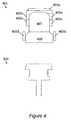
- FIG. 4is a cross-sectional depiction of the hollow cathode magnetron (HCM) apparatus suitable for practicing the current invention.
- HCMhollow cathode magnetron
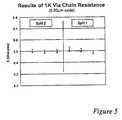
- FIG. 5represents experimental data showing resistance data from wafer samples run with and without separate preclean steps.
- FIG. 6represents experimental data showing stress migration data from wafer samples run with and without separate preclean steps.
- waferwill be used interchangeably with “partially fabricated integrated circuit.”
- partially fabricated integrated circuitcan refer to a silicon wafer during any of many stages of integrated circuit fabrication thereon.
- wafer substrateand “substrate” are all used interchangeably.
- FIG. 3Apresents aspects of a process flow for forming diffusion barriers in wafers that contain unlanded vias.
- the process flowsare performed in the context of copper Damascene processing.
- FIGS. 1A-1FOne can refer back to FIGS. 1A-1F for a slightly broader context.
- a diffusion barrierwill be formed thereon.
- methods that etch through barrier material at the bottom of viasmay be used. These methods were referred to previously in the background section. Since the majority of wafer substrates will have unlanded vias (as discussed in the background section in reference to FIG. 1F ), the methods of the present invention address cases in which unlanded vias exist. These methods provide for a minimal amount of barrier material at the bottom of the vias and lower sidewalls so the copper diffusion and copper seed contamination issues described earlier can be avoided.
- a method of forming diffusion barriers of the invention intended primarily, but not exclusively, for unlanded vias,will now be described with reference to the flow chart of FIG. 3A and associated schematic diagrams in FIGS. 3B-3H .
- each of the depicted process operationsis carried out using process conditions and materials specific to a particular desired outcome.
- the inventionis not limited to these specific embodiments, but rather they are intended to illustrate the invention.
- process block 301first the wafer is heated under vacuum to degas the wafer surface of contaminants such as water and volatile hydrocarbons from the etch residue of the previous process. The wafer is then transferred to another chamber where it is cooled in such a manner as to not allow condensation and recontamination.
- Suitable chamber temperatures for the degassing processrange from about 200 to 400 degrees Celsius, more preferably around 300 degrees Celsius.
- the cooling processis typically done at room temperature or below.
- the methods of this inventionare performed without using a preclean step.
- Experimental evidencehas shown that the process operations depicted in FIG. 3A are sufficient to provide a diffusion barrier substantially free of the deleterious contaminants that precleaning is intended to remove.
- some alternative embodiments of the inventionallow for a preclean operation 301 ′ in addition to the degassing process step 301 of FIG. 3A .
- This preclean steptypically involves implementing a sputter etch or reactive clean process using gas mixtures of argon and hydrogen or nitrogen and hydrogen, or oxygen containing mixtures. If this preclean process is used, it is preferable that the degassing and preclean processes be done in separate chambers to avoid contamination after the preclean step.
- the simultaneous etch/deposition(as described below) is used to remove surface contaminants from the via bottom by etching through a barrier material thereon.
- the barrieris removed only at the via bottom and the exposed copper is effectively cleaned by exposure to the plasma, thereby eliminating the need for a preclean step.
- Contaminantsinclude residues left from etch and photoresist clean processes and oxides of copper in some instances.
- the elimination of a preclean stepprovides various advantages. For example, during the preclean step, copper can sputter onto the walls of the vias, which, after subsequent process steps, can lead to copper that is trapped between the dielectric material and the diffusion barrier material on the via walls.
- Precleaningcan widen trench openings thereby preventing critical dimensions from being realized. Precleaning can also increase the dielectric constant of low-k dielectrics by extracting carbon from the dielectric matrix (due to reaction with hydrogen). And, typically, precleaning requires a separate process chamber, thereby increasing the process complexity.
- Substrate 302includes a pre-formed dielectric layer 309 (such as fluorine or carbon doped silicon dioxide, porous silicon dioxide, or organic-containing low-k materials) with etched line paths (trenches and vias) in which a diffusion barrier 311 has been deposited followed by inlaying with copper conductive route 313 .
- a silicon nitride or silicon carbide barrier layer 315was laid thereon, followed by another layer of dielectric material, 317 . After process steps (including lithography) for example as outlined in the background section above, dielectric layer 317 has etched trench 321 and via 323 .
- the surface area at the bottom of via 323includes a portion of exposed copper conductive route 313 and a portion of exposed dielectric 309 .
- the exposure of the dielectric layer 309is undesirable since subsequent deposition of copper into the trench 321 and via 323 regions will allow for direct copper-dielectric contact, thereby allowing copper to diffuse through the dielectric layer 309 in later wafer processing and causing electrical leakages.
- the next block in the process flowinvolves depositing a first portion of the diffusion barrier over the surface of the wafer. See 303 .
- Deposition of the first portion of the diffusion barriermay be done using PVD, CVD or ALD.
- the first portion of the diffusion barrierincludes at least one of tantalum, nitrogen-doped tantalum, tantalum nitride, and titanium silicon nitride. Tantalum, nitrogen-doped tantalum, and tantalum nitride are preferably deposited using PVD.
- other materials for which the invention is applicableinclude but are not limited to tungsten, cobalt, and other refractory nitrides (e.g. TiN, WN x ).
- Suitable DC power for the PVD sputter targetrange between about 10 and 50 kW when not significantly biasing the wafer, with a preferred DC power range between about 15 and 30 kW.
- Titanium silicon nitrideis preferably deposited using CVD or ALD.
- suitable thicknesses for the first portion of barrier materialrange between about 10 and 400 angstroms, preferably between about 50 and 200 angstroms, as measured over field regions on the surface of the wafer.
- the thicknesses of the barrier materialrange between about 10 and 100 angstroms, preferably between about 15 and 50 angstroms, as measured over the field regions on the surface of the wafer.
- FIG. 3Cdepicts substrate 302 , after deposition of the first portion of the diffusion barrier.
- the first portionis a monolayer 325 that covers all surfaces of substrate 302 .
- the monolayeris between about 10 and 400 angstroms thick on the field of the wafer, more preferably between about 50 and 200 angstroms thick. Note that debris 320 remains at the bottom of the via.
- the term “monolayer”is meant to mean a single layer of material, not necessarily a single atomic or molecular layer as the term is sometimes used.
- a bilayer or a trilayeris preferred for the first, second, third or subsequent portions of diffusion barrier material.
- the inventionis not limited to deposition of a particular number of layers. Essentially any thickness of diffusion barrier material may be deposited: fractional layers, monolayers, bilayers, trilayers, etc.
- PVD methods in generalwill often provide less conformal barrier layer coverage compared to CVD and ALD methods.
- FIGS. 3C-3Hdepict a more conformal barrier layer deposition, more representative of a CVD or ALD methods. Since preferred methods typically employ PVD, the resulting barrier layers in these cases may be less conformal than depicted in FIGS. 3C-3H .
- the second portion of the diffusion barrieris a sputtered metal. Even more preferably, the sputtered metal is tantalum.
- FIG. 3Ddepicts substrate 302 after such an etch/deposition process in which the etch to deposition ratio was greater than 1, both in the bottom of via 323 and on the horizontal surfaces (field 319 and step 322 (see FIG. 3B )).
- the relative rate of etchwas controlled such that step 322 and field 319 were minimally etched relative to the bottom of via 323 .
- the first portion 325is etched through at the bottom of via 323 , exposing the surface of the copper conductive route 313 and the surface of the dielectric layer 309 . See 335 .
- barrier material 329(the second portion) is deposited on the sidewalls of the via and trench.
- the second portionwill have between about 25 and 100 ⁇ of barrier material.
- the resulting structure 302has a diffusion barrier (bilayer) that includes continuous first portion 325 and discontinuous second portion 329 .
- etching at the bottom of the viahas redistributed residue 320 to the lower sidewalls of the via. See residue 320 ′.
- the second portion of the barrier layeris deposited only on the sidewalls of the surface features of substrate 302 .
- some methods of the inventionuse etch to deposition ratios greater than one at the via bottom, but less than one on the field and trench regions.
- the second portion of barrier materialwill be deposited on the field and trench as well as the sidewalls.
- the second portionhas between about 0 and 100 ⁇ of barrier material deposited on the field and horizontal trench surfaces. It is generally desirable to minimize the thickness of the material to reduce CMP costs in later wafer production processes.
- a third portion of barrier materialis deposited to once again cover the exposed dielectric material at the bottoms of the vias and any contamination (sputtered copper, copper oxide, etch residue, and/or sputtered dielectric) on the lower via side wall. See 307 .
- the purpose of this depositionis to cover the surface of the underlying dielectric layer that was exposed during the etch of the previous step as well as cover any contamination that exists at the lower side wall to avoid the seed contamination issues described earlier.
- the amount of barrier material at the bottoms of the viasis preferably minimal so as to minimize the resistance between the underlying copper conductive route and subsequently deposited copper conductor.
- Deposition of this third portion of barrier materialcan be carried out using conventional PVD, CVD or ALD techniques as described above for deposition of the first portion of the barrier layer. Since it is not feasible to accurately measure the thickness of barrier material at the bottoms of vias using current technology, the thickness of the field regions after the deposition is typically used as reference points. If deposited by PVD, this thickness is between about 10 and 400 angstroms, preferably between about 50 and 200 angstroms as measured at the field regions of the wafer. If deposited by CVD or ALD, the filed thickness is between 10 and 50 A. In both cases the field thickness is selected to obtain between about 10 and 50 angstroms of diffusion barrier material in the via bottoms.
- FIG. 3Edepicts substrate 302 , after deposition of the third portion of barrier layer.
- the third portionis a monolayer 337 that covers all surfaces of the substrate 302 .
- the monolayeris preferably between about 10 and 400 angstroms thick on the field of the wafer, more preferably about 50 to 200 angstroms thick. Note that the result of this deposition is barrier layer coverage of the surfaces of both the underlying dielectric layer 309 and the copper conductive route 313 . Hence, the subsequently deposited copper seed layer is prevented from contacting the dielectric layer.
- layer 337will cover and immobilize any residues 320 ′ sputtered onto the via sidewall from the underlying copper layer 313 or dielectric 309 during etching operation 305 .
- residuesare known to interfere with subsequent deposition of copper seed layers onto the via sidewall, resulting in poor adhesion, seed discontinuity, and fill voiding.
- By encapsulating such residues 320 ′ under layer 337these problems are eliminated or mitigated.
- next block in the process flowis an optional process involving the etching of the third portion of the diffusion barrier without etching all the way through to the underlying metal and dielectric layers. See 308 . If, for instance, the third portion of the barrier layer was deposited too thickly, this process removes some of the barrier layer at the bottom of the via. This process is similar to the process of block 305 in that some barrier layer will simultaneously be deposited elsewhere on the wafer. However, since the sidewalls of the vias are nominally already sufficiently covered by the first, second and third portions of barrier layer, sidewall coverage may be less significant. Of course, any number of subsequent barrier material deposition and/or etch steps may be added until a desired final via bottom barrier material thickness is achieved.
- FIG. 3Gdepicts a substrate 302 after optional etch/deposition process 308 .
- the rate of etchwas controlled such that at least the bottom of via 323 is etched to leave a minimal amount of barrier material 341 .
- barrier material 337may be deposited on the sidewalls of the via and trench. See region 329 ′.
- etch/deposition processes described in process blocks 305 and 308 of FIG. 3Aare preferably carried out using RF re-sputtering techniques.
- one method using this techniqueincludes sputtering a metal from target having an applied DC power of between about 1 and 30 kW while applying a RF bias to the wafer substrate.
- Suitable wafer substrate biasesrange between about 100 and 2000 Watts, preferably 200-1200 Watts. Note that the choice of DC and RF power depends on the substrate size, thus the wide range in power.
- a preferable carrier gas for the RF re-sputtering techniqueis argon, however, other gases such as N 2 , Ne and Xe can also be used.
- Suitable gas flow raterange between about 50 and 300 sccm.
- FIGS. 3F and 3Hdepict substrate 302 after deposition of metal conductive layers 339 and 343 , respectively.
- the metal conductive layersare copper seed layers, but the invention is not limited to seed layers.
- Diffusion barrier stack structurescan provide better protection against metal diffusion than single layers due to the combined properties of the individual layers of which they are made.
- multi-layered diffusion barrierscan also be made thicker to serve as a fill element.
- lithographyleaves the dielectric with undercuts (notches) or bowing (concavity) in the sidewalls. These defects can be repaired by deposition of extra barrier material that fills the defects. Judicious combinations of CVD, ALD and PVD methods are used to achieve this end.
- methods of the inventionemploy a simultaneous etch/deposition to etch barrier material at the via bottom while depositing barrier material elsewhere on a wafer substrate.
- various aspects of process flowsinvolve deposition of barrier materials (by ALD, CVD or PVD), precleaning, and degassing operations. In preferred embodiments all these process steps are done in the same processing tool.
- Tools that allow degas, ALD or CVD deposition, and PVD deposition all under the same vacuumare the INOVA and INOVA xT deposition systems available from Novellus Systems of San Jose, Calif. These system are comprised of processing modules, e.g. for Degas, Cool, Preclean, PVD, CVD or ALD processes, mounted to the same wafer handling module.
- a waferis placed into the apparatus, it is degassed, cooled, and optionally precleaned (for example with an argon plasma). Then, a first deposited layer of barrier material is formed via PVD (e.g. tantalum nitride). Next, a tantalum simultaneous etch/deposition process is carried out which deposits the second portion of the diffusion barrier and etches at least the bottom of the via, forming the final diffusion barrier structure. Finally, a third layer of tantalum is deposited by PVD.
- PVDe.g. tantalum nitride
- the simultaneous etch/deposition stepsare carried out using a hollow cathode magnetron (HCM) sputtering module.
- HCMhollow cathode magnetron
- Such devicesare described in U.S. Pat. Nos. 5,482,611, naming Helmer et al. as inventors, 6,179,973 B1 and 6,193,854 B1, naming Lai et al. as inventors, and 6,217,716 B1 naming Lai as the inventor. Each of these patents is incorporated herein by reference for all purposes. If the barrier material to be deposited is tantalum or tantalum nitride, a tantalum target source is used.
- a suitable apparatusemploys a magnetic array for generating a confined plasma of high ion density.
- the magnetic arraymay be implemented as one or more electromagnets, permanent magnets, or some combination of electromagnets and permanent magnets.
- the apparatusmay include other magnets located proximate the substrate region for promoting process uniformity.
- FIG. 4presents a simple cross sectional view of one type of HCM sputtering apparatus that can be used in accordance with the invention.
- the HCM apparatushas two main components, the source 401 , in which a plasma is created and maintained, and the RF bias electrostatic chuck (ESC) pedestal 403 , which secures the wafer and applies an RF bias on the wafer, if needed.
- the source 401contains four electromagnets 405 a - 405 d , a cathode target 407 and an anode 409 .
- the cathode target 407generally has a hollow cup-like shape so that plasma formed in the source can be concentrated within this hollow region.
- the cathode target 407also serves as a sputter target and is, therefore, made of a metal material such as tantalum, which is to be deposited onto a substrate.
- An inert gassuch as argon
- An intense magnetic fieldis produced by electromagnets 405 a - 405 d within the cathode target region.
- An additional four electromagnetsare arranged downstream of the cathode target so that different currents can be applied to each electromagnet, thereby producing an ion flux and a controlled deposition and/or etch rate and uniformity.
- An anode 409typically held at plasma floating potential, is used, in conjunction with the source electromagnets to shape the plasma distribution at the target mouth.
- the RF bias ESC pedestal 403holds the wafer substrate in place and can apply a RF bias to the wafer substrate.
- the ion energy, and therefore the deposition and/or etch ratecan also be controlled by the pedestal RF bias.
- An additional function of the ESC pedestalis to provide wafer temperature control during deposition and resputtering.
- argon backside gasis used to provide thermal coupling between the substrate and the ESC. In many cases, the ESC is cooled during deposition.
- a plasma reactorthat allows fine control of the plasma conditions can be tuned to provide the E/D variations over substrate topology as desired for certain embodiments this invention.
- the INOVA HCM reactors provided by Novellus Systemshave eight or more separate electromagnetic coils. Each of these, and particularly those located near the substrate, can be independently controlled to fine tune the E/D profile from via bottom to field region and from the center to edge across of the wafer.
- Preferred process conditionsinclude a pressure of between about 0.1 and 100 mTorr.
- Argon process flowsare between about 50 and 300 SCCM (standard cubic centimeters per minute).
- SCCMstandard cubic centimeters per minute.
- E/D>1is desired both at the bottom of the vias and in the field
- a DC source powerof between about 1 and 10 kW is applied to the tantalum target.
- the electromagnet coil currents usedare between about 0-10 A. The current polarity and current levels are optimized to obtain uniform deposition and resputter across the wafer surface, as well as to maximize utilization of the target.
- the wafer temperatureis manipulated using a temperature controlled stage, the wafer temperatures used are between about ⁇ 100 and 100° C., preferably about ⁇ 20° C.
- the waferis biased with an RF frequency source located below or in proximity to the stage.
- the RF power appliedis preferably between about 100 and 2000 W.
- the amount of sputteringis controlled by the RF power at fixed RF frequency.
- Various RF frequenciescan be used to achieve this effect.
- One preferred RF frequencyis 13.56 MHz.
- etch rateis most strongly related to the RF power, while the deposition rate is most strongly related to the DC source power.
- the E/D ratiodepends predominantly on the ratio of RF power (table) to DC power (source). Higher RF/DC power ratios correspond to higher the E/D ratios on the wafer.
- the etch rateis largely dependent on RF power and pressure since these parameters control the energy of argon ions near the wafer.
- the deposition rateis largely dependent on DC power since this parameter affects the flux and energy of argon ions near the surface target.
- Controlling the plasma potential and the DC bias on the wafercan provide the etch conditions required for this invention.
- the energy of the argon ions, and therefore the etch rateis proportional to the difference between plasma potential and wafer potential.
- the deposition rate during re-sputteringis proportional to the DC power applied to the HCM target.
- the deposition rate in the trench and viais reduced due to the off-normal component of the material (tantalum) flux.
- the etch rate at the trench and via bottomis almost independent on the feature geometry due to the high directionality of argon ion flux.
- EOn the sidewall, E ⁇ 0, resulting in net deposition.
- the etch/deposition ratio (E/D)can be controlled so that it is >1 in the via bottom and (resulting in a net etching), and >1 or ⁇ 1 on the trench and field horizontal surfaces.
- the magnitude of E/D on the side wallsis ⁇ 1 because the plasma flux is directed primarily toward the wafer surface (parallel with the side walls).
- only horizontal surfaceswith relatively large surface areas (compared to the side walls) are effectively etched by the impinging plasma flux.
- the sidewallsreceive a net deposition.
- tantalum nitride or nitrogen-doped tantalumis the barrier material to be deposited
- a nitrogen sourcesuch as N 2 will be used at 5-100 SCCM, preferably about 10-50 SCCM in conjunction with argon.
- Titanium silicon nitrideis deposited by CVD using a technique described in U.S. patent application Ser. No. 09/965,471, entitled “Method of Depositing a Diffusion Barrier for Copper Interconnection Applications” filed by Suwwan de Felipe on the same date as this application, or U.S. patent application Ser. No. 09/862,539, titled “Improved Deposition of Conformal Copper Seed Layers by Control of Barrier Layer Morphology” filed by Suwwan de Felipe on May 21, 2001.
- methods of the inventionform bilayered or trilayered diffusion barriers in unlanded via structures.
- Illustrative structures of diffusion barriers of the inventionwere described above with reference to the figures.
- the table belowsummarizes further aspects of some preferred embodiments of the invention.
- Each of the thirteen listed diffusion barriersmay vary according to the particular thickness of the deposited layers, and whether or not material is deposited only on the side walls or on the side walls and the field and horizontal trench regions during the simultaneous etch deposition (E/D) process step. Therefore this table is meant to emphasize some preferred stack compositions as well as particular methods used to form them.
- the symbol “Ta(N)”is meant to designate tantalum with some nitrogen content.
- Titanium silicon nitrideis designated by “TiN(Si).” Note that all examples listed in table below provide some minimal barrier coverage at via bottom and avoid the above-described problems of copper on copper contact.
- the simultaneous etch/deposition operation(Barrier Material 2) is presented as a metallic tantalum deposition (as opposed to a nitride deposition).
- the etch/deposition operationmay be conducted in a nitrogen-containing atmosphere to form a nitride (of tantalum or other metal).
- the processes of this inventionallow for deposition in which any combination of metallic materials, nitrides, or other compositions (metal silicon nitrides) are deposited in the three or four barrier material deposition operations.
- some of the processes of this inventionare performed without using a preclean step prior to deposition the first portion of the diffusion barrier ( FIG. 3A , process block 303 ). It is noteworthy to point out that the elimination of the separate preclean is contrary to previous typical methods. As discussed previously, traditionally, the preclean typically involves an argon sputter etch or reactive sputter to remove contaminants such as copper oxide and residues from etch and photoresist processes. However, experimental evidence in accordance with the present invention show that process steps described in the present invention can sufficiently clean the substrate surface and that a separate preclean step is not necessary, and may even be detrimental. FIGS. 5 and 6 show experimental data to support these claims.
- FIG. 5shows electrical resistance of a 1000-via chain with 0.3 micron width.
- the resistance valuesare shown for two different process splits.
- Split 1the control group, was treated with a standard preclean step, which involves the equivalent of about 100 angstroms oxide removal.
- Split 2was run without a preclean process.
- degas steps using 40 seconds of degas step at 350 degrees Celsiuswere implemented.
- Barrier layers in both splitswere processed using the following: 100 ⁇ HCM TaN deposition, 150 ⁇ re-sputtering (via bottom etched through), 250 ⁇ HCM Ta deposition, 125 ⁇ re-sputtering (via bottom partially etched).
- 800 ⁇ of copper seedwas deposited over the barrier layers. Data from three wafers of each split were measured.
- split 1right side of graph
- split 2left side of graph
- the barrier processwas sufficient in cleaning the via bottoms such that the separate preclean step can be eliminated.
- FIG. 6shows results from a stress migration test of the same two splits used in FIG. 5 .
- Stress migrationis a measurement of the shift in via or chain resistance after thermally cycling the wafer between certain temperatures over a specified time period. In this experiment, the wafers underwent six thermal cycles between 150 and 250 degrees Celsius for a period of twelve hours.
- FIG. 6shows the probability (vertical axis) of via chain resistance shifts (in %) for each of the splits. Data from split 1 (precleaned) is represented with triangle symbols while data from split 2 (not precleaned) is represented with solid circle symbols.
- split 1 resultsshow a significant shift in via chain resistance while split 2 results show substantially no shift in via chain resistance.
Landscapes
- Engineering & Computer Science (AREA)
- Physics & Mathematics (AREA)
- Condensed Matter Physics & Semiconductors (AREA)
- General Physics & Mathematics (AREA)
- Manufacturing & Machinery (AREA)
- Computer Hardware Design (AREA)
- Microelectronics & Electronic Packaging (AREA)
- Power Engineering (AREA)
- Internal Circuitry In Semiconductor Integrated Circuit Devices (AREA)
Abstract
Description
This application is a continuation claiming priority under 35 USC 120 from U.S. patent application Ser. No. 10/804,353 filed Mar. 18, 2004 (now U.S. Pat. No. 7,186,648), titled “Barrier First Method For Single Damascene Trench Applications,” naming Rozbicki et al. as inventors, which is a continuation-in-part claiming priority under 35 USC 120 from U.S. patent application Ser. No. 10/412,562 filed Apr. 11, 2003 (now U.S. Pat. No. 6,764,940), which is a continuation-in-part claiming priority under 35 USC 120 from U.S. patent application Ser. No. 09/965,472 filed Sep. 26, 2001 (now U.S. Pat. No. 6,607,977), which claims benefit of prior U.S. Provisional Application No. 60/275,803 filed Mar. 13, 2001. U.S. Pat. No. 6,764,940 also claims benefit of U.S. Provisional Patent Application No. 60/379,874 filed May 10, 2002. Each of these references is incorporated herein by reference in its entirety for all purposes.
The present invention pertains to methods for forming a metal diffusion barrier on a partially fabricated integrated circuit. The methods employ at least one operation that selectively etches barrier material from the bottom of vias while simultaneously depositing barrier material on most regions of the integrated circuit. The methods are frequently performed on unlanded vias.
Integrated circuit (IC) manufacturers have traditionally used aluminum and aluminum alloys, among other metals, as the conductive metal for integrated circuits. While copper has a greater conductivity than aluminum, it has not been used because of certain challenges it presents, including the fact that it readily diffuses into silicon oxide and degrades insulating electrical properties even at very low concentrations. Recently, however, IC manufacturers have been turning to copper because of its high conductivity and electromigration resistance, among other desirable properties. Most notable among the IC metalization processes that use copper is Damascene processing. Damascene processing is often a preferred method because it requires fewer processing steps than other methods and offers a higher yield. It is also particularly well suited to metals such as Cu that cannot readily be patterned by plasma etching.
Damascene processing is a method for forming interconnections on integrated circuits. It involves formation of inlaid metal lines in trenches and vias formed in a dielectric layer (inter-metal dielectric). In order to frame the context of this invention, a brief description of a copper dual Damascene process for forming a partially fabricated integrated circuit is described below. Note that the invention applies to other fabrication processes including single Damascene processes.
Presented inFIGS. 1A-1F , is a cross sectional depiction device structures created at various stages of a dual Damascene fabrication process. A cross sectional depiction of a completed structure created by the dual Damascene process is shown inFIG. 2 . Referring toFIG. 1A , an example of a typical substrate,100, used for dual Damascene fabrication is illustrated.Substrate 100 includes a pre-formed dielectric layer103 (such as fluorine or carbon doped silicon dioxide or organic-containing low-k materials) with etched line paths (trenches and vias) in which adiffusion barrier 105 has been deposited followed by inlaying with copperconductive routes 107. Because copper or other mobile conductive material provides the conductive paths of the semiconductor wafer, the underlying silicon devices must be protected from metal ions (e.g., Cu2+) that might otherwise diffuse or drift into the silicon. Suitable materials fordiffusion barrier 105 include tantalum, tantalum nitride, tungsten, titanium tungsten, titanium nitride, tungsten nitride, and the like. In a typical process,barrier 105 is formed by a physical vapor deposition (PVD) process such as sputtering, a chemical vapor deposition (CVD) process, or an atomic layer deposition (ALD) process. Typical metals for the conductive routes are aluminum and copper. More frequently, copper serves as the metal in Damascene processes, as depicted in these figures. The resultant partially fabricatedintegrated circuit 100 is a representative substrate for subsequent Damascene processing, as depicted inFIGS. 1B-1F .
As depicted inFIG. 1B , a silicon nitride or siliconcarbide diffusion barrier 109 is deposited to encapsulateconductive routes 107. Next, a first dielectric layer,111, of a dual Damascene dielectric structure is deposited ondiffusion barrier 109. This is followed by deposition of an etch-stop layer113 (typically composed of silicon nitride or silicon carbide) on the firstdielectric layer 111.
The process follows, as depicted inFIG. 1C , where a seconddielectric layer 115 of the dual Damascene dielectric structure is deposited in a similar manner to the firstdielectric layer 111, onto etch-stop layer 113. Deposition of anantireflective layer 117, typically a silicon oxynitride, follows.
The dual Damascene process continues, as depicted inFIGS. 1D-1E , with etching of vias and trenches in the first and second dielectric layers. First,vias 119 are etched throughantireflective layer 117 and the seconddielectric layer 115. Standard lithography techniques are used to etch a pattern of these vias. The etching ofvias 119 is controlled such that etch-stop layer 113 is not penetrated. As depicted inFIG. 1E , in a subsequent lithography process,antireflective layer 117 is removed andtrenches 121 are etched in the seconddielectric layer 115;vias 119 are propagated through etch-stop layer 113, firstdielectric layer 111, anddiffusion barrier 109.
Next, as depicted inFIG. 1F , these newly formed vias and trenches are, as described above, coated with adiffusion barrier 123. As mentioned above,barrier 123 is made of tantalum, or other materials that effectively block diffusion of copper atoms into the dielectric layers.
Afterdiffusion barrier 123 is deposited, a seed layer of copper is applied (typically a PVD process) to enable subsequent electrofilling of the features with copper inlay.FIG. 2 shows the completed dual Damascene process, in which copperconductive routes 125 are inlayed (seed layer not depicted) into the via and trench surfaces overbarrier 123.
Thus, to reduce resistance between the copper routes, a portion of the diffusion barrier may be etched away, specifically at the via bottom, in order to expose the lower copper plug. This approach is generally described in U.S. Pat. No. 6,287,977 to Hashim et al., U.S. Pat. No. 5,985,762 to Geffken et al., and U.S. patent application Ser. No. 09/965,472 filed Sep. 26, 2001, incorporated by reference above. By completely etching away the barrier in the via bottom, the subsequent copper inlay can be deposited directly onto the lower copper line. Conventional methods for etching away diffusion barriers at the bottom of vias (for example, the region ofbarrier 127 contactingcopper inlay 107 inFIG. 1F ) are problematic in that they are not selective enough. That is, conventional etch methods remove barrier material from undesired areas as well, such as the corners (edges) of the via, trench, and field regions. This can destroy critical dimensions of the via and trench surfaces (faceting of the corners) and unnecessarily exposes the dielectric to plasma. This may lead to dielectric damage, such as critical dimension loss, increase in dielectric constant (with concomitant negative impact on device speed), and poor adhesion to the barrier layer. These problems will be encountered with the method described in the Geffken et al. patent.
Further, when etching through barrier layers and into the underlying copper metal, some copper oxide and etch residues (including polymeric etch residues) are sputtered onto the barrier sidewall. In the unlanded via case, dielectric material is sputtered along with the underlying copper metal onto the barrier side wall. Subsequently, when a copper seed layer is deposited, it forms directly on these contaminants. As a consequence, the copper seed layer may exhibit a myriad of problems, including poor adhesion, seed discontinuity, fill voiding, etc. Each of these problems negatively impact device performance, yield, and reliability. Such issues are expected with the method described in the Hashim et al. patent.
In addition, conventional etching methods do not address “unlanded” via regions typical of modern devices. In some cases these unlanded vias do not fully overlap with theunderlying copper inlay 107. Such unlanded via is illustrated inFIG. 1F wherein a portion ofdiffusion barrier 123 is located at viabottom 127. In the unlanded via case, a portion of the barrier rests oncopper inlay 107 and a portion rests ondielectric 103. A conventional barrier etch, meant to exposecopper inlay 107, would expose bothcopper inlay 107 and dielectric103 inregion 127. If copper were to be deposited on such structure, it could diffuse directly intodielectric 103 throughregion 127. The Hashim et al. patent mentioned above does not also address this problem.
What are therefore needed are improved methods of forming diffusion barriers on integrated circuit structures, selective methods in which the diffusion barrier thickness is minimized at the bottoms of vias without sacrificing the integrity of the diffusion barrier in other regions. Preferably, this is accomplished in a manner that accounts for the special considerations of unlanded vias.
The present invention pertains to methods for forming a metal diffusion barrier on an integrated circuit. It provides a continuous, relatively thin barrier coverage at via bottoms for good reliability (even when unlanded vias are used) and low via resistance. The invention also provides a sufficiently thick barrier coverage on via sidewalls to address reliability issues such as stress migration and electromigration resistance. By selectively etching at the via bottoms, and not necessarily elsewhere, the invention also minimizes corner “blow-out” and faceting of vias without changing in feature critical dimensions. Still further, the invention minimizes copper contamination during wafer manufacturing processes and preserves properties of inter-level dielectrics by eliminating or minimizing direct plasma exposure. In general, methods of this invention lower wafer manufacturing costs by increasing yield.
The present invention pertains to various methods for forming a diffusion barrier. When integrated with a seed layer deposition operation, the method typically includes at least four operations. The first operation deposits barrier material via PVD, CVD or ALD to provide some minimal coverage. The second operation deposits an additional barrier material and simultaneously etches a portion of the barrier material deposited in the first operation. In cases in which unlanded vias may exist (and in some instances in which unlanded vias do not exist), a third operation is performed wherein at least a small amount of a barrier material is deposited over at least the bottoms of the vias to protect the dielectric material of the previous interconnect layer. The third operation uses at least one of PVD, CVD or ALD techniques. Typically, the barrier material deposited in the third operation covers at least the lower sidewalls of the vias (in addition to the via bottoms) and provides a high quality template on which to deposit a subsequent metal conductive layer. In some embodiments, at least part of the second operation is performed in the same processing chamber as the third operation. The forth operation deposits a metal conductive layer over the substrate to form a conductive route to the next metalization layer. In preferred embodiments of the invention, all four operations are done in a single process tool without breaking vacuum. In some embodiments, an additional operation is performed between the third and forth operation. This operation deposits another portion of barrier material and simultaneously etches a portion of the barrier material deposited in the third operation.
In preferred embodiments of the invention, a degas operation is performed prior to the first operation. The purpose of the degas operation is to remove unwanted moisture and hydrocarbon etch residue that may exist on the wafer. The degas operation can be performed by heating the wafer to between about 200 to 400 degrees Celsius, for example, depending on the type of dielectric and other materials in the device.
The result of the operations is a metal diffusion barrier formed in part by net etching in certain areas, in particular the bottom of vias, and a net deposition in other areas, in particular the sidewalls of vias. Controlled etching is used to selectively remove barrier material from the bottom of vias, either completely or partially, thus reducing the resistance of subsequently formed metal interconnects. In a preferred embodiment of the invention, selective etching is also used to remove contaminants under the barrier material, thus obviating a separate preclean operation before the first operation. In alternative embodiments, the preclean operation is performed before the first operation.
The invention accomplishes simultaneous etch and deposition by creation of defined plasma producing process conditions such that barrier material is etched away in some regions while in other regions diffusion barrier material is deposited. This is the second of the four operations described previously. The descriptive term “etch to deposition ratio” or “E/D” is used herein to characterize process conditions at any position on substrate. More specifically, in the context of a partially fabricated integrated circuit having via and trench surface features, methods described herein provide that E/D varies as a function of the elevation profile of the surface features to which the plasma is applied. Generally, E/D is greatest at the bottommost regions of the wafer surface features and decreases in magnitude as elevation increases. At a position where there is no net gain or loss of material, the etch and deposition processes equal each other and the E/D is 1. So preferably, the E/D is greater than 1 at the via bottom, but may be less than 1 on the trench step and on the field region.
A preferred diffusion barrier material for this etch/deposition sputter is tantalum, although the invention is not limited to tantalum. Other materials for which the invention is applicable include but are not limited to tungsten, cobalt, solid solutions (interstitial forms) of tantalum and nitrogen and binary nitrides (e.g. TaNx, TiN, WNx). After diffusion barriers of the invention are formed, a metal conductive layer is deposited thereon.
Preferably methods of the invention are used in Damascene processing in which the metal conductive layer and interconnects are made of copper. In some preferred methods of the invention, the metal conductive layer is a copper seed layer. Preferably seed layers of the invention are formed using PVD, but the invention is not limited in this way. As mentioned, in some methods of the invention, all aspects of a process flow for forming a diffusion barrier and depositing a metal conductive route thereon are done in the same processing tool. While a preferred conductive metal material for this deposition is copper, the invention is not limited to copper. Other materials for which the invention is applicable include aluminum and conductive alloys of aluminum or copper.
Methods of the invention create diffusion barriers having stack structures. Distinct portions of each stack may be deposited (layered) using PVD, CVD, ALD or other methods. Thus diffusion barriers of the invention may have monolayered, bilayered, trilayered or multilayered structures. Preferably, the portions include at least one of tantalum, nitrogen-doped tantalum, tantalum nitride, and titanium silicon nitride. More detail of preferred arrangements for the layering of these materials, methods of depositing, and structure of the diffusion barriers formed therefrom, will be described in the detailed description below.
Methods of the invention create diffusion barriers within integrated circuitry using at least the materials described above. Therefore, another aspect of the invention pertains to an integrated circuit or a partially fabricated integrated circuit. Preferably integrated circuits or partially fabricated integrated circuits of the invention include a diffusion barrier which covers all surfaces of a plurality of vias and a plurality of trenches with minimal diffusion barrier material at the bottom of the plurality of vias, and a metal conductive layer provided thereon, such that the diffusion barrier provides relatively little resistance to electrical conduction between the metal conductive layer and the plurality of metal conductive routes at the bottom of the plurality of vias.
A diffusion barrier which covers all surfaces of a plurality of vias and a plurality of trenches, said diffusion barrier having a thickness of between about 50 and 400 Å on said surfaces except at the bottom of the plurality of vias where there is less than about 50 Å of diffusion barrier material; and a metal conductive layer provided thereon.
These and other features and advantages of the present invention will be described in more detail below with reference to the associated drawings.
In the following detailed description of the present invention, numerous specific embodiments are set forth in order to provide a thorough understanding of the invention. However, as will be apparent to those skilled in the art, the present invention may be practiced without these specific details or by using alternate elements or processes. In other instances well-known processes, procedures and components have not been described in detail so as not to unnecessarily obscure aspects of the present invention.
In this application, the term “wafer” will be used interchangeably with “partially fabricated integrated circuit.” One skilled in the art would understand that the term “partially fabricated integrated circuit” can refer to a silicon wafer during any of many stages of integrated circuit fabrication thereon. Thus, “wafer”, “wafer substrate”, and “substrate” are all used interchangeably.
As mentioned, the invention finds particular use in Damascene processing. More particularly, the invention is useful in applications in which a diffusion barrier is deposited on partially fabricated integrated circuits that contain unlanded vias to prevent copper diffusion into surrounding dielectric material.FIG. 3A presents aspects of a process flow for forming diffusion barriers in wafers that contain unlanded vias. Typically, the process flows are performed in the context of copper Damascene processing. One can refer back toFIGS. 1A-1F for a slightly broader context.
Specifically, referring toFIG. 1E , once vias and trenches have been formed in a wafer, typically a diffusion barrier will be formed thereon. For wafer substrates having vias that are entirely landed over underlying metal surfaces, methods that etch through barrier material at the bottom of vias may be used. These methods were referred to previously in the background section. Since the majority of wafer substrates will have unlanded vias (as discussed in the background section in reference toFIG. 1F ), the methods of the present invention address cases in which unlanded vias exist. These methods provide for a minimal amount of barrier material at the bottom of the vias and lower sidewalls so the copper diffusion and copper seed contamination issues described earlier can be avoided.
A method of forming diffusion barriers of the invention intended primarily, but not exclusively, for unlanded vias, will now be described with reference to the flow chart ofFIG. 3A and associated schematic diagrams inFIGS. 3B-3H . Note that in many embodiments, each of the depicted process operations is carried out using process conditions and materials specific to a particular desired outcome. The invention is not limited to these specific embodiments, but rather they are intended to illustrate the invention.
Referring toFIG. 3A , aspects of a process flow for forming a diffusion barrier of the invention are depicted. According to process block301, first the wafer is heated under vacuum to degas the wafer surface of contaminants such as water and volatile hydrocarbons from the etch residue of the previous process. The wafer is then transferred to another chamber where it is cooled in such a manner as to not allow condensation and recontamination. Suitable chamber temperatures for the degassing process range from about 200 to 400 degrees Celsius, more preferably around 300 degrees Celsius. The cooling process is typically done at room temperature or below.
Preferably, the methods of this invention are performed without using a preclean step. Experimental evidence (see EXPERIMENTAL section) has shown that the process operations depicted inFIG. 3A are sufficient to provide a diffusion barrier substantially free of the deleterious contaminants that precleaning is intended to remove. Nevertheless, some alternative embodiments of the invention allow for apreclean operation 301′ in addition to thedegassing process step 301 ofFIG. 3A . This preclean step typically involves implementing a sputter etch or reactive clean process using gas mixtures of argon and hydrogen or nitrogen and hydrogen, or oxygen containing mixtures. If this preclean process is used, it is preferable that the degassing and preclean processes be done in separate chambers to avoid contamination after the preclean step. In preferred embodiments, the simultaneous etch/deposition (as described below) is used to remove surface contaminants from the via bottom by etching through a barrier material thereon. In this way, the barrier is removed only at the via bottom and the exposed copper is effectively cleaned by exposure to the plasma, thereby eliminating the need for a preclean step. Contaminants include residues left from etch and photoresist clean processes and oxides of copper in some instances. The elimination of a preclean step provides various advantages. For example, during the preclean step, copper can sputter onto the walls of the vias, which, after subsequent process steps, can lead to copper that is trapped between the dielectric material and the diffusion barrier material on the via walls. In addition, sputter precleaning can widen trench openings thereby preventing critical dimensions from being realized. Precleaning can also increase the dielectric constant of low-k dielectrics by extracting carbon from the dielectric matrix (due to reaction with hydrogen). And, typically, precleaning requires a separate process chamber, thereby increasing the process complexity.
Referring toFIG. 3B , a typical substrate with an unlanded via,302, is illustrated.Substrate 302 includes a pre-formed dielectric layer309 (such as fluorine or carbon doped silicon dioxide, porous silicon dioxide, or organic-containing low-k materials) with etched line paths (trenches and vias) in which adiffusion barrier 311 has been deposited followed by inlaying with copperconductive route 313. A silicon nitride or siliconcarbide barrier layer 315 was laid thereon, followed by another layer of dielectric material,317. After process steps (including lithography) for example as outlined in the background section above,dielectric layer 317 has etchedtrench 321 and via323. Note that included in this surface feature are horizontal surfaces (field 319, step322 oftrench 321, and the bottom of via323) and vertical surfaces (the side walls of the via and trench). As shown, somedebris 320, such as copper oxide and etch residue, typically exists at the bottom of via323. Since via323 is unlanded, the surface area at the bottom of via323 includes a portion of exposed copperconductive route 313 and a portion of exposeddielectric 309.
As described previously, the exposure of thedielectric layer 309 is undesirable since subsequent deposition of copper into thetrench 321 and via323 regions will allow for direct copper-dielectric contact, thereby allowing copper to diffuse through thedielectric layer 309 in later wafer processing and causing electrical leakages. To prevent direct copper-dielectric contact in this viaregion 323, it is preferred to cover the exposeddielectric layer 309 with barrier material before copper deposition. Methods to achieve this will be discussed shortly.
Referring back toFIG. 3A , the next block in the process flow involves depositing a first portion of the diffusion barrier over the surface of the wafer. See303. Deposition of the first portion of the diffusion barrier may be done using PVD, CVD or ALD. Preferably, the first portion of the diffusion barrier includes at least one of tantalum, nitrogen-doped tantalum, tantalum nitride, and titanium silicon nitride. Tantalum, nitrogen-doped tantalum, and tantalum nitride are preferably deposited using PVD. As mentioned, other materials for which the invention is applicable include but are not limited to tungsten, cobalt, and other refractory nitrides (e.g. TiN, WNx). These materials would also preferably be deposited by PVD. Suitable DC power for the PVD sputter target range between about 10 and 50 kW when not significantly biasing the wafer, with a preferred DC power range between about 15 and 30 kW. Titanium silicon nitride is preferably deposited using CVD or ALD. If deposited by PVD, suitable thicknesses for the first portion of barrier material range between about 10 and 400 angstroms, preferably between about 50 and 200 angstroms, as measured over field regions on the surface of the wafer. If deposited by CVD or ALD, the thicknesses of the barrier material range between about 10 and 100 angstroms, preferably between about 15 and 50 angstroms, as measured over the field regions on the surface of the wafer.
Note that the term “monolayer” is meant to mean a single layer of material, not necessarily a single atomic or molecular layer as the term is sometimes used. In some embodiments, a bilayer or a trilayer is preferred for the first, second, third or subsequent portions of diffusion barrier material. The invention is not limited to deposition of a particular number of layers. Essentially any thickness of diffusion barrier material may be deposited: fractional layers, monolayers, bilayers, trilayers, etc. Note that PVD methods in general will often provide less conformal barrier layer coverage compared to CVD and ALD methods.FIGS. 3C-3H depict a more conformal barrier layer deposition, more representative of a CVD or ALD methods. Since preferred methods typically employ PVD, the resulting barrier layers in these cases may be less conformal than depicted inFIGS. 3C-3H .
Referring back toFIG. 3A , once the first portion of the diffusion barrier is deposited, simultaneous etch/deposition is used to etch through the first portion of the diffusion barrier at the bottom of the vias while depositing a second portion of the diffusion barrier elsewhere on the wafer. See305. Preferably the second portion of the diffusion barrier is a sputtered metal. Even more preferably, the sputtered metal is tantalum.
Referring back toFIG. 3D , the second portion of the barrier layer is deposited only on the sidewalls of the surface features ofsubstrate 302. As mentioned, some methods of the invention use etch to deposition ratios greater than one at the via bottom, but less than one on the field and trench regions. In this case, the second portion of barrier material will be deposited on the field and trench as well as the sidewalls. Preferably, the second portion has between about 0 and 100 Å of barrier material deposited on the field and horizontal trench surfaces. It is generally desirable to minimize the thickness of the material to reduce CMP costs in later wafer production processes.
Referring again toFIG. 3A , once the first portion of the diffusion barrier is etched through at the bottoms of the vias and a second portion of diffusion barrier is simultaneously deposited, a third portion of barrier material is deposited to once again cover the exposed dielectric material at the bottoms of the vias and any contamination (sputtered copper, copper oxide, etch residue, and/or sputtered dielectric) on the lower via side wall. See307. The purpose of this deposition is to cover the surface of the underlying dielectric layer that was exposed during the etch of the previous step as well as cover any contamination that exists at the lower side wall to avoid the seed contamination issues described earlier. The amount of barrier material at the bottoms of the vias is preferably minimal so as to minimize the resistance between the underlying copper conductive route and subsequently deposited copper conductor. Deposition of this third portion of barrier material can be carried out using conventional PVD, CVD or ALD techniques as described above for deposition of the first portion of the barrier layer. Since it is not feasible to accurately measure the thickness of barrier material at the bottoms of vias using current technology, the thickness of the field regions after the deposition is typically used as reference points. If deposited by PVD, this thickness is between about 10 and 400 angstroms, preferably between about 50 and 200 angstroms as measured at the field regions of the wafer. If deposited by CVD or ALD, the filed thickness is between 10 and 50 A. In both cases the field thickness is selected to obtain between about 10 and 50 angstroms of diffusion barrier material in the via bottoms.
Note thatlayer 337 will cover and immobilize anyresidues 320′ sputtered onto the via sidewall from theunderlying copper layer 313 or dielectric309 duringetching operation 305. As indicated above, such residues are known to interfere with subsequent deposition of copper seed layers onto the via sidewall, resulting in poor adhesion, seed discontinuity, and fill voiding. By encapsulatingsuch residues 320′ underlayer 337, these problems are eliminated or mitigated.
Referring back toFIG. 3A , the next block in the process flow is an optional process involving the etching of the third portion of the diffusion barrier without etching all the way through to the underlying metal and dielectric layers. See308. If, for instance, the third portion of the barrier layer was deposited too thickly, this process removes some of the barrier layer at the bottom of the via. This process is similar to the process ofblock 305 in that some barrier layer will simultaneously be deposited elsewhere on the wafer. However, since the sidewalls of the vias are nominally already sufficiently covered by the first, second and third portions of barrier layer, sidewall coverage may be less significant. Of course, any number of subsequent barrier material deposition and/or etch steps may be added until a desired final via bottom barrier material thickness is achieved.
The etch/deposition processes described in process blocks305 and308 ofFIG. 3A are preferably carried out using RF re-sputtering techniques. For example, one method using this technique includes sputtering a metal from target having an applied DC power of between about 1 and 30 kW while applying a RF bias to the wafer substrate. Suitable wafer substrate biases range between about 100 and 2000 Watts, preferably 200-1200 Watts. Note that the choice of DC and RF power depends on the substrate size, thus the wide range in power. A preferable carrier gas for the RF re-sputtering technique is argon, however, other gases such as N2, Ne and Xe can also be used. Suitable gas flow rate range between about 50 and 300 sccm.
Referring again toFIG. 3A , once the diffusion barrier is formed and an appropriate amount of barrier material exists on the bottoms of the vias, a metal conductive layer is deposited over the surface of the wafer such that the metal conductive layer is separated from the underlying metal layer by the small amount of barrier material at the bottom of the vias. See310.FIGS. 3F and 3H depictsubstrate 302 after deposition of metalconductive layers FIG. 3A is done.
As illustrated inFIGS. 3F and 3H , newly deposited metalconductive layers copper route 313 by regions of the diffusion barrier having minimal thickness. Preferably between about 25 and 300 Å are removed to provide this minimal thickness.Substrate
Diffusion barrier stack structures (bilayers, trilayers, etc.) can provide better protection against metal diffusion than single layers due to the combined properties of the individual layers of which they are made. In some cases, multi-layered diffusion barriers can also be made thicker to serve as a fill element. For example, in some low-k dielectric applications, lithography leaves the dielectric with undercuts (notches) or bowing (concavity) in the sidewalls. These defects can be repaired by deposition of extra barrier material that fills the defects. Judicious combinations of CVD, ALD and PVD methods are used to achieve this end.
As mentioned, methods of the invention employ a simultaneous etch/deposition to etch barrier material at the via bottom while depositing barrier material elsewhere on a wafer substrate. As well, various aspects of process flows involve deposition of barrier materials (by ALD, CVD or PVD), precleaning, and degassing operations. In preferred embodiments all these process steps are done in the same processing tool. Tools that allow degas, ALD or CVD deposition, and PVD deposition all under the same vacuum are the INOVA and INOVA xT deposition systems available from Novellus Systems of San Jose, Calif. These system are comprised of processing modules, e.g. for Degas, Cool, Preclean, PVD, CVD or ALD processes, mounted to the same wafer handling module. Therefore, once a wafer is in the tool and a vacuum is established, all of the above described process aspects are performed without breaking vacuum. For example, a wafer is placed into the apparatus, it is degassed, cooled, and optionally precleaned (for example with an argon plasma). Then, a first deposited layer of barrier material is formed via PVD (e.g. tantalum nitride). Next, a tantalum simultaneous etch/deposition process is carried out which deposits the second portion of the diffusion barrier and etches at least the bottom of the via, forming the final diffusion barrier structure. Finally, a third layer of tantalum is deposited by PVD.
Preferably the simultaneous etch/deposition steps are carried out using a hollow cathode magnetron (HCM) sputtering module. Such devices are described in U.S. Pat. Nos. 5,482,611, naming Helmer et al. as inventors, 6,179,973 B1 and 6,193,854 B1, naming Lai et al. as inventors, and 6,217,716 B1 naming Lai as the inventor. Each of these patents is incorporated herein by reference for all purposes. If the barrier material to be deposited is tantalum or tantalum nitride, a tantalum target source is used.
In some embodiments, a suitable apparatus employs a magnetic array for generating a confined plasma of high ion density. The magnetic array may be implemented as one or more electromagnets, permanent magnets, or some combination of electromagnets and permanent magnets. The apparatus may include other magnets located proximate the substrate region for promoting process uniformity.
An inert gas, such as argon, is introduced to into the hollow region of thecathode target 407 to form a plasma. An intense magnetic field is produced by electromagnets405a-405dwithin the cathode target region. An additional four electromagnets are arranged downstream of the cathode target so that different currents can be applied to each electromagnet, thereby producing an ion flux and a controlled deposition and/or etch rate and uniformity. Ananode 409, typically held at plasma floating potential, is used, in conjunction with the source electromagnets to shape the plasma distribution at the target mouth. The RF biasESC pedestal 403 holds the wafer substrate in place and can apply a RF bias to the wafer substrate. The ion energy, and therefore the deposition and/or etch rate can also be controlled by the pedestal RF bias. An additional function of the ESC pedestal is to provide wafer temperature control during deposition and resputtering. Typically, argon backside gas is used to provide thermal coupling between the substrate and the ESC. In many cases, the ESC is cooled during deposition.
Generally, a plasma reactor that allows fine control of the plasma conditions can be tuned to provide the E/D variations over substrate topology as desired for certain embodiments this invention. The INOVA HCM reactors provided by Novellus Systems have eight or more separate electromagnetic coils. Each of these, and particularly those located near the substrate, can be independently controlled to fine tune the E/D profile from via bottom to field region and from the center to edge across of the wafer.
Preferred process conditions include a pressure of between about 0.1 and 100 mTorr. Argon process flows are between about 50 and 300 SCCM (standard cubic centimeters per minute). When E/D>1 is desired both at the bottom of the vias and in the field, a DC source power of between about 1 and 10 kW is applied to the tantalum target. The electromagnet coil currents used are between about 0-10 A. The current polarity and current levels are optimized to obtain uniform deposition and resputter across the wafer surface, as well as to maximize utilization of the target.
The wafer temperature is manipulated using a temperature controlled stage, the wafer temperatures used are between about −100 and 100° C., preferably about −20° C. The wafer is biased with an RF frequency source located below or in proximity to the stage. The RF power applied is preferably between about 100 and 2000 W. In preferred embodiments, the amount of sputtering is controlled by the RF power at fixed RF frequency. Various RF frequencies can be used to achieve this effect. One preferred RF frequency is 13.56 MHz.
In general, etch rate is most strongly related to the RF power, while the deposition rate is most strongly related to the DC source power. The E/D ratio depends predominantly on the ratio of RF power (table) to DC power (source). Higher RF/DC power ratios correspond to higher the E/D ratios on the wafer. The etch rate is largely dependent on RF power and pressure since these parameters control the energy of argon ions near the wafer. The deposition rate is largely dependent on DC power since this parameter affects the flux and energy of argon ions near the surface target.
Controlling the plasma potential and the DC bias on the wafer can provide the etch conditions required for this invention. The energy of the argon ions, and therefore the etch rate, is proportional to the difference between plasma potential and wafer potential. The deposition rate during re-sputtering is proportional to the DC power applied to the HCM target. However, the deposition rate in the trench and via is reduced due to the off-normal component of the material (tantalum) flux. The etch rate at the trench and via bottom is almost independent on the feature geometry due to the high directionality of argon ion flux. These effects lead to the following E/D relationships during the resputter step: E/D (via bottom)>E/D (trench bottom)>E/D (field)>E/D (sidewall). On the sidewall, E˜0, resulting in net deposition. Thus, the etch/deposition ratio (E/D) can be controlled so that it is >1 in the via bottom and (resulting in a net etching), and >1 or <1 on the trench and field horizontal surfaces. The magnitude of E/D on the side walls is <1 because the plasma flux is directed primarily toward the wafer surface (parallel with the side walls). Thus, only horizontal surfaces (with relatively large surface areas (compared to the side walls)) are effectively etched by the impinging plasma flux. The sidewalls receive a net deposition.
If tantalum nitride or nitrogen-doped tantalum is the barrier material to be deposited, a nitrogen source such as N2will be used at 5-100 SCCM, preferably about 10-50 SCCM in conjunction with argon. Titanium silicon nitride is deposited by CVD using a technique described in U.S. patent application Ser. No. 09/965,471, entitled “Method of Depositing a Diffusion Barrier for Copper Interconnection Applications” filed by Suwwan de Felipe on the same date as this application, or U.S. patent application Ser. No. 09/862,539, titled “Improved Deposition of Conformal Copper Seed Layers by Control of Barrier Layer Morphology” filed by Suwwan de Felipe on May 21, 2001.
As mentioned, methods of the invention form bilayered or trilayered diffusion barriers in unlanded via structures. Illustrative structures of diffusion barriers of the invention were described above with reference to the figures. The table below summarizes further aspects of some preferred embodiments of the invention. Each of the thirteen listed diffusion barriers may vary according to the particular thickness of the deposited layers, and whether or not material is deposited only on the side walls or on the side walls and the field and horizontal trench regions during the simultaneous etch deposition (E/D) process step. Therefore this table is meant to emphasize some preferred stack compositions as well as particular methods used to form them. The symbol “Ta(N)” is meant to designate tantalum with some nitrogen content. This can be nitrogen-doped tantalum, solid solutions (interstitial forms) of tantalum and nitrogen, or tantalum nitrides. Titanium silicon nitride is designated by “TiN(Si).” Note that all examples listed in table below provide some minimal barrier coverage at via bottom and avoid the above-described problems of copper on copper contact.
| TABLE |
| Exemplary Diffusion Barriers of the Invention. |
| Barrier | Barrier | Barrier | Barrier |
| Diffusion | Pre- | Material 1 | Material 2 | Material 3 | Material 4 |
| Barrier | clean | (303) | (305) | (307) | (308) |
| 1 | yes | HCM Ta(N) | Ta E/D etch | — | — |
| partial | |||||
| 2 | yes | HCM Ta(N) | Ta E/D etch | HCM Ta(N) | |
| through | |||||
| 3 | yes | HCM Ta(N) | Ta E/D etch | HCM Ta(N) | Ta E/D |
| through | etch | ||||
| partial | |||||
| 4 | yes | CVD | Ta E/D etch | ||
| TiN(Si) | partial | ||||
| 5 | yes | CVD | Ta E/D etch | HCM Ta(N) | |
| TiN(Si) | through | ||||
| 6 | yes | CVD | Ta E/D etch | HCM Ta(N) | Ta E/D |
| TiN(Si) | through | etch | |||
| partial | |||||
| 7 | no | HCM Ta(N) | Ta E/D etch | HCM Ta(N) | |
| through | |||||
| 8 | no | HCM Ta(N) | Ta E/D etch | HCM Ta(N) | Ta E/D |
| through | etch | ||||
| partial | |||||
| 9 | no | CVD | Ta E/D etch | HCM Ta(N) | |
| TiN(Si) | through | ||||
| 10 | no | CVD | Ta E/D etch | HCM Ta(N) | Ta E/D |
| TiN(Si) | through | etch | |||
| partial | |||||
| 11 | no | HCM Ta(N) | Ta E/D etch | CVD | |
| through | TiN(Si) | ||||
| 12 | no | HCM Ta(N) | Ta E/D etch | ALD Ta(N) | |
| through | |||||
| 13 | no | ALD Ta(N) | Ta E/D etch | HCM Ta | |
| through | |||||
Note that in the above examples, the simultaneous etch/deposition operation (Barrier Material 2) is presented as a metallic tantalum deposition (as opposed to a nitride deposition). In some embodiments of the invention, the etch/deposition operation may be conducted in a nitrogen-containing atmosphere to form a nitride (of tantalum or other metal). Generally, the processes of this invention allow for deposition in which any combination of metallic materials, nitrides, or other compositions (metal silicon nitrides) are deposited in the three or four barrier material deposition operations.
As mentioned previously, in preferred embodiments of the invention, some of the processes of this invention are performed without using a preclean step prior to deposition the first portion of the diffusion barrier (FIG. 3A , process block303). It is noteworthy to point out that the elimination of the separate preclean is contrary to previous typical methods. As discussed previously, traditionally, the preclean typically involves an argon sputter etch or reactive sputter to remove contaminants such as copper oxide and residues from etch and photoresist processes. However, experimental evidence in accordance with the present invention show that process steps described in the present invention can sufficiently clean the substrate surface and that a separate preclean step is not necessary, and may even be detrimental.FIGS. 5 and 6 show experimental data to support these claims.
As shown byFIG. 5 , split1 (right side of graph) and split2 (left side of graph) exhibit similar via chain resistance values (about 0.5 Ohms/via) and distribution of resistance values. Therefore, one could speculate that the barrier process was sufficient in cleaning the via bottoms such that the separate preclean step can be eliminated.
InFIG. 6 , split1 results show a significant shift in via chain resistance whilesplit 2 results show substantially no shift in via chain resistance. These results indicate that thesplit 2, the wafers processed without using a separate preclean step, actually show better stress migration results and are, therefore, more reliable.
Although various details have been omitted for clarity's sake, various design alternatives may be implemented. Therefore, the present examples are to be considered as illustrative and not restrictive, and the invention is not to be limited to the details given herein, but may be modified within the scope of the appended claims.
Claims (20)
1. A method for depositing a diffusion barrier and a metal conductive layer on a wafer substrate, the method comprising:
(a) depositing a first portion of the diffusion barrier over the surface of the wafer substrate;
(b) etching through at least part of the first portion of the diffusion barrier at bottom portions of a plurality of vias to expose at least part of an underlying metal layer, while simultaneously depositing a second portion of the diffusion barrier on at least field regions of the wafer substrate, wherein the etching comprises removing the diffusion barrier material by impinging on the substrate with energetic inert gas ions;
(c) depositing a third portion of the diffusion barrier, which covers at least the bottoms of the vias; and
(d) depositing the metal conductive layer over the surface of the wafer substrate, such that the metal conductive layer is deposited on the third portion of the diffusion barrier at least at the bottom portions of the plurality of vias.
2. The method ofclaim 1 , wherein (b) comprises sputtering metal from a negatively biased metal target in a PVD process chamber resulting in net deposition at least in the field region.
3. The method ofclaim 1 , wherein the substrate comprises a plurality of unlanded vias.
4. The method ofclaim 1 , further comprising etching the third portion of diffusion barrier at least at the bottom portions of the vias without fully etching through such that an amount of the metal-containing material remains at the bottoms of the vias prior to (d).
5. The method ofclaim 1 , wherein (b) comprises removing contaminants from a top portion of the underlying metal layer, while simultaneously depositing the second portion of the diffusion barrier material at least on the field region.
6. The method ofclaim 1 , wherein in (b) an etch rate to deposition rate ratio is less than 1 at a bottom portion of a trench.
7. A method for depositing a diffusion barrier and a metal conductive layer on a wafer substrate comprising a plurality of unlanded vias, the method comprising:
(a) depositing a first portion of the diffusion barrier over the surface of the wafer substrate;
(b) etching through at least part of the first portion of the diffusion barrier at the bottoms of the plurality of unlanded vias to expose at least part of an underlying metal layer and a dielectric layer, while simultaneously depositing a second portion of the diffusion barrier on at least field regions of the wafer substrate;
(c) depositing a third portion of the diffusion barrier, which covers at least the bottoms of the vias; and
(d) depositing the metal conductive layer over the surface of the wafer substrate, such that the metal conductive layer is deposited on the third portion of the diffusion barrier at least at the bottom portions of the plurality of vias.
8. The method ofclaim 7 , wherein (b) comprises sputtering metal from a negatively biased metal target in a PVD process chamber resulting in net deposition at least in the field region.
9. The method ofclaim 8 , wherein in (b) the etching comprises removing the diffusion barrier material by impinging on the substrate with energetic inert gas ions.
10. The method ofclaim 7 , further comprising etching the third portion of diffusion barrier at least at the bottom portions of the vias without fully etching through such that an amount of the metal-containing material remains at the bottoms of the vias prior to (d).
11. The method ofclaim 7 , wherein (b) comprises removing contaminants from a top portion of the underlying metal layer, while simultaneously depositing the second portion of the diffusion barrier material at least on the field region.
12. The method ofclaim 7 , wherein in (b) an etch rate to deposition rate ratio is less than 1 at a bottom portion of a trench.
13. The method ofclaim 7 , further comprising heating the wafer to between about 200 to 400° C. prior to (a) to remove unwanted moisture.
14. The method ofclaim 7 , wherein method does not employ a precleaning operation prior to (a).
15. The method ofclaim 7 , wherein at least two successive operations in (a) through (c) are performed in the same processing chamber.
16. The method ofclaim 15 , wherein the processing chamber comprises a hollow cathode magnetron.
17. The method ofclaim 7 , wherein the diffusion barrier layer deposited in (a) comprises a material selected from the group consisting of W, Ti, and Ta nitrides, and wherein the metal conductive layer deposited in (d) comprises Cu.
18. The method ofclaim 1 , wherein the diffusion barrier layer deposited in (a) comprises a material selected from the group consisting of W, Ti, and Ta nitrides, and wherein the metal conductive layer deposited in (d) comprises Cu.
19. The method ofclaim 1 , further comprising heating the wafer to between about 200 to 400° C. prior to (a) to remove unwanted moisture.
20. The method ofclaim 7 , wherein at least two successive operations in (a) through (c) are performed in the same processing chamber comprising a hollow cathode magnetron.
Priority Applications (4)
| Application Number | Priority Date | Filing Date | Title |
|---|---|---|---|
| US11/714,465US7732314B1 (en) | 2001-03-13 | 2007-03-05 | Method for depositing a diffusion barrier for copper interconnect applications |
| US13/904,464US8679972B1 (en) | 2001-03-13 | 2013-05-29 | Method of depositing a diffusion barrier for copper interconnect applications |
| US14/171,590US9099535B1 (en) | 2001-03-13 | 2014-02-03 | Method of depositing a diffusion barrier for copper interconnect applications |
| US14/755,800US9508593B1 (en) | 2001-03-13 | 2015-06-30 | Method of depositing a diffusion barrier for copper interconnect applications |
Applications Claiming Priority (6)
| Application Number | Priority Date | Filing Date | Title |
|---|---|---|---|
| US27580301P | 2001-03-13 | 2001-03-13 | |
| US09/965,472US6607977B1 (en) | 2001-03-13 | 2001-09-26 | Method of depositing a diffusion barrier for copper interconnect applications |
| US37987402P | 2002-05-10 | 2002-05-10 | |
| US10/412,562US6764940B1 (en) | 2001-03-13 | 2003-04-11 | Method for depositing a diffusion barrier for copper interconnect applications |
| US10/804,353US7186648B1 (en) | 2001-03-13 | 2004-03-18 | Barrier first method for single damascene trench applications |
| US11/714,465US7732314B1 (en) | 2001-03-13 | 2007-03-05 | Method for depositing a diffusion barrier for copper interconnect applications |
Related Parent Applications (1)
| Application Number | Title | Priority Date | Filing Date |
|---|---|---|---|
| US10/804,353ContinuationUS7186648B1 (en) | 2001-03-13 | 2004-03-18 | Barrier first method for single damascene trench applications |
Related Child Applications (1)
| Application Number | Title | Priority Date | Filing Date |
|---|---|---|---|
| US76487010AContinuation | 2001-03-13 | 2010-04-21 |
Publications (1)
| Publication Number | Publication Date |
|---|---|
| US7732314B1true US7732314B1 (en) | 2010-06-08 |
Family
ID=37807113
Family Applications (2)
| Application Number | Title | Priority Date | Filing Date |
|---|---|---|---|
| US10/804,353Expired - LifetimeUS7186648B1 (en) | 2001-03-13 | 2004-03-18 | Barrier first method for single damascene trench applications |
| US11/714,465Expired - LifetimeUS7732314B1 (en) | 2001-03-13 | 2007-03-05 | Method for depositing a diffusion barrier for copper interconnect applications |
Family Applications Before (1)
| Application Number | Title | Priority Date | Filing Date |
|---|---|---|---|
| US10/804,353Expired - LifetimeUS7186648B1 (en) | 2001-03-13 | 2004-03-18 | Barrier first method for single damascene trench applications |
Country Status (1)
| Country | Link |
|---|---|
| US (2) | US7186648B1 (en) |
Cited By (17)
| Publication number | Priority date | Publication date | Assignee | Title |
|---|---|---|---|---|
| US20090001590A1 (en)* | 2007-06-27 | 2009-01-01 | Sanyo Electric Co., Ltd. | Wiring structure and method of manufacturing the same |
| US20110021020A1 (en)* | 2006-09-20 | 2011-01-27 | Fujitsu Semiconductor Limited | Semiconductor device and fabrication process thereof |
| US7897516B1 (en) | 2007-05-24 | 2011-03-01 | Novellus Systems, Inc. | Use of ultra-high magnetic fields in resputter and plasma etching |
| US8017523B1 (en) | 2008-05-16 | 2011-09-13 | Novellus Systems, Inc. | Deposition of doped copper seed layers having improved reliability |
| US8043484B1 (en) | 2001-03-13 | 2011-10-25 | Novellus Systems, Inc. | Methods and apparatus for resputtering process that improves barrier coverage |
| US20120153480A1 (en)* | 2010-12-16 | 2012-06-21 | Globalfoundries Inc. | Metallization Systems of Semiconductor Devices Comprising a Copper/Silicon Compound as a Barrier Material |
| US8298933B2 (en) | 2003-04-11 | 2012-10-30 | Novellus Systems, Inc. | Conformal films on semiconductor substrates |
| US8298936B1 (en) | 2007-02-01 | 2012-10-30 | Novellus Systems, Inc. | Multistep method of depositing metal seed layers |
| WO2012134801A3 (en)* | 2011-03-29 | 2013-01-03 | International Business Machines Corporation | Stacked via structure for metal fuse applications |
| US20130234259A1 (en)* | 2012-03-06 | 2013-09-12 | Young Ho Yang | Semiconductor device and method of manufacturing the same |
| US20130307151A1 (en)* | 2012-05-16 | 2013-11-21 | International Business Machines Corporation | Method to resolve hollow metal defects in interconnects |
| US8679972B1 (en) | 2001-03-13 | 2014-03-25 | Novellus Systems, Inc. | Method of depositing a diffusion barrier for copper interconnect applications |
| US8765596B1 (en) | 2003-04-11 | 2014-07-01 | Novellus Systems, Inc. | Atomic layer profiling of diffusion barrier and metal seed layers |
| US8858763B1 (en) | 2006-11-10 | 2014-10-14 | Novellus Systems, Inc. | Apparatus and methods for deposition and/or etch selectivity |
| CN104538347A (en)* | 2014-12-31 | 2015-04-22 | 上海华虹宏力半导体制造有限公司 | Contact hole technological method |
| WO2021150280A1 (en)* | 2020-01-24 | 2021-07-29 | Applied Materials, Inc. | Methods and devices for subtractive self-alignment |
| US11508617B2 (en) | 2019-10-24 | 2022-11-22 | Applied Materials, Inc. | Method of forming interconnect for semiconductor device |
Families Citing this family (395)
| Publication number | Priority date | Publication date | Assignee | Title |
|---|---|---|---|---|
| US8696875B2 (en) | 1999-10-08 | 2014-04-15 | Applied Materials, Inc. | Self-ionized and inductively-coupled plasma for sputtering and resputtering |
| US10047430B2 (en) | 1999-10-08 | 2018-08-14 | Applied Materials, Inc. | Self-ionized and inductively-coupled plasma for sputtering and resputtering |
| US6498091B1 (en)* | 2000-11-01 | 2002-12-24 | Applied Materials, Inc. | Method of using a barrier sputter reactor to remove an underlying barrier layer |
| US7186648B1 (en) | 2001-03-13 | 2007-03-06 | Novellus Systems, Inc. | Barrier first method for single damascene trench applications |
| US7781327B1 (en) | 2001-03-13 | 2010-08-24 | Novellus Systems, Inc. | Resputtering process for eliminating dielectric damage |
| US7390755B1 (en) | 2002-03-26 | 2008-06-24 | Novellus Systems, Inc. | Methods for post etch cleans |
| US7504006B2 (en) | 2002-08-01 | 2009-03-17 | Applied Materials, Inc. | Self-ionized and capacitively-coupled plasma for sputtering and resputtering |
| US7288484B1 (en) | 2004-07-13 | 2007-10-30 | Novellus Systems, Inc. | Photoresist strip method for low-k dielectrics |
| US8193096B2 (en) | 2004-12-13 | 2012-06-05 | Novellus Systems, Inc. | High dose implantation strip (HDIS) in H2 base chemistry |
| US8129281B1 (en) | 2005-05-12 | 2012-03-06 | Novellus Systems, Inc. | Plasma based photoresist removal system for cleaning post ash residue |
| US20070257366A1 (en)* | 2006-05-03 | 2007-11-08 | Taiwan Semiconductor Manufacturing Company, Ltd. | Barrier layer for semiconductor interconnect structure |
| US7645696B1 (en) | 2006-06-22 | 2010-01-12 | Novellus Systems, Inc. | Deposition of thin continuous PVD seed layers having improved adhesion to the barrier layer |
| US7855147B1 (en) | 2006-06-22 | 2010-12-21 | Novellus Systems, Inc. | Methods and apparatus for engineering an interface between a diffusion barrier layer and a seed layer |
| US7740768B1 (en) | 2006-10-12 | 2010-06-22 | Novellus Systems, Inc. | Simultaneous front side ash and backside clean |
| KR100790452B1 (en)* | 2006-12-28 | 2008-01-03 | 주식회사 하이닉스반도체 | Multi-layer metallization method of semiconductor device using damascene process |
| DE102007004860B4 (en)* | 2007-01-31 | 2008-11-06 | Advanced Micro Devices, Inc., Sunnyvale | A method of making a copper-based metallization layer having a conductive overcoat by an improved integration scheme |
| US8435895B2 (en) | 2007-04-04 | 2013-05-07 | Novellus Systems, Inc. | Methods for stripping photoresist and/or cleaning metal regions |
| US7922880B1 (en) | 2007-05-24 | 2011-04-12 | Novellus Systems, Inc. | Method and apparatus for increasing local plasma density in magnetically confined plasma |
| US7659197B1 (en) | 2007-09-21 | 2010-02-09 | Novellus Systems, Inc. | Selective resputtering of metal seed layers |
| US8591661B2 (en) | 2009-12-11 | 2013-11-26 | Novellus Systems, Inc. | Low damage photoresist strip method for low-K dielectrics |
| US10378106B2 (en) | 2008-11-14 | 2019-08-13 | Asm Ip Holding B.V. | Method of forming insulation film by modified PEALD |
| US9394608B2 (en) | 2009-04-06 | 2016-07-19 | Asm America, Inc. | Semiconductor processing reactor and components thereof |
| US8802201B2 (en) | 2009-08-14 | 2014-08-12 | Asm America, Inc. | Systems and methods for thin-film deposition of metal oxides using excited nitrogen-oxygen species |
| US20110143548A1 (en)* | 2009-12-11 | 2011-06-16 | David Cheung | Ultra low silicon loss high dose implant strip |
| US8721797B2 (en)* | 2009-12-11 | 2014-05-13 | Novellus Systems, Inc. | Enhanced passivation process to protect silicon prior to high dose implant strip |
| US9312155B2 (en) | 2011-06-06 | 2016-04-12 | Asm Japan K.K. | High-throughput semiconductor-processing apparatus equipped with multiple dual-chamber modules |
| US10364496B2 (en) | 2011-06-27 | 2019-07-30 | Asm Ip Holding B.V. | Dual section module having shared and unshared mass flow controllers |
| US10854498B2 (en) | 2011-07-15 | 2020-12-01 | Asm Ip Holding B.V. | Wafer-supporting device and method for producing same |
| US20130023129A1 (en) | 2011-07-20 | 2013-01-24 | Asm America, Inc. | Pressure transmitter for a semiconductor processing environment |
| US9613825B2 (en) | 2011-08-26 | 2017-04-04 | Novellus Systems, Inc. | Photoresist strip processes for improved device integrity |
| US9017481B1 (en) | 2011-10-28 | 2015-04-28 | Asm America, Inc. | Process feed management for semiconductor substrate processing |
| US9558931B2 (en) | 2012-07-27 | 2017-01-31 | Asm Ip Holding B.V. | System and method for gas-phase sulfur passivation of a semiconductor surface |
| US9659799B2 (en) | 2012-08-28 | 2017-05-23 | Asm Ip Holding B.V. | Systems and methods for dynamic semiconductor process scheduling |
| US9021985B2 (en) | 2012-09-12 | 2015-05-05 | Asm Ip Holdings B.V. | Process gas management for an inductively-coupled plasma deposition reactor |
| US10714315B2 (en) | 2012-10-12 | 2020-07-14 | Asm Ip Holdings B.V. | Semiconductor reaction chamber showerhead |
| US20160376700A1 (en) | 2013-02-01 | 2016-12-29 | Asm Ip Holding B.V. | System for treatment of deposition reactor |
| US9589770B2 (en) | 2013-03-08 | 2017-03-07 | Asm Ip Holding B.V. | Method and systems for in-situ formation of intermediate reactive species |
| US9484191B2 (en) | 2013-03-08 | 2016-11-01 | Asm Ip Holding B.V. | Pulsed remote plasma method and system |
| US8993054B2 (en) | 2013-07-12 | 2015-03-31 | Asm Ip Holding B.V. | Method and system to reduce outgassing in a reaction chamber |
| US9240412B2 (en) | 2013-09-27 | 2016-01-19 | Asm Ip Holding B.V. | Semiconductor structure and device and methods of forming same using selective epitaxial process |
| US9605343B2 (en) | 2013-11-13 | 2017-03-28 | Asm Ip Holding B.V. | Method for forming conformal carbon films, structures conformal carbon film, and system of forming same |
| US10683571B2 (en) | 2014-02-25 | 2020-06-16 | Asm Ip Holding B.V. | Gas supply manifold and method of supplying gases to chamber using same |
| US10167557B2 (en) | 2014-03-18 | 2019-01-01 | Asm Ip Holding B.V. | Gas distribution system, reactor including the system, and methods of using the same |
| US11015245B2 (en) | 2014-03-19 | 2021-05-25 | Asm Ip Holding B.V. | Gas-phase reactor and system having exhaust plenum and components thereof |
| US9514954B2 (en) | 2014-06-10 | 2016-12-06 | Lam Research Corporation | Peroxide-vapor treatment for enhancing photoresist-strip performance and modifying organic films |
| US10858737B2 (en) | 2014-07-28 | 2020-12-08 | Asm Ip Holding B.V. | Showerhead assembly and components thereof |
| US9890456B2 (en) | 2014-08-21 | 2018-02-13 | Asm Ip Holding B.V. | Method and system for in situ formation of gas-phase compounds |
| US9657845B2 (en) | 2014-10-07 | 2017-05-23 | Asm Ip Holding B.V. | Variable conductance gas distribution apparatus and method |
| US10941490B2 (en) | 2014-10-07 | 2021-03-09 | Asm Ip Holding B.V. | Multiple temperature range susceptor, assembly, reactor and system including the susceptor, and methods of using the same |
| KR102300403B1 (en) | 2014-11-19 | 2021-09-09 | 에이에스엠 아이피 홀딩 비.브이. | Method of depositing thin film |
| KR102263121B1 (en) | 2014-12-22 | 2021-06-09 | 에이에스엠 아이피 홀딩 비.브이. | Semiconductor device and manufacuring method thereof |
| US10529542B2 (en) | 2015-03-11 | 2020-01-07 | Asm Ip Holdings B.V. | Cross-flow reactor and method |
| US10276355B2 (en) | 2015-03-12 | 2019-04-30 | Asm Ip Holding B.V. | Multi-zone reactor, system including the reactor, and method of using the same |
| US10458018B2 (en) | 2015-06-26 | 2019-10-29 | Asm Ip Holding B.V. | Structures including metal carbide material, devices including the structures, and methods of forming same |
| US10600673B2 (en) | 2015-07-07 | 2020-03-24 | Asm Ip Holding B.V. | Magnetic susceptor to baseplate seal |
| US10043661B2 (en) | 2015-07-13 | 2018-08-07 | Asm Ip Holding B.V. | Method for protecting layer by forming hydrocarbon-based extremely thin film |
| US10083836B2 (en) | 2015-07-24 | 2018-09-25 | Asm Ip Holding B.V. | Formation of boron-doped titanium metal films with high work function |
| US10087525B2 (en) | 2015-08-04 | 2018-10-02 | Asm Ip Holding B.V. | Variable gap hard stop design |
| US9647114B2 (en) | 2015-08-14 | 2017-05-09 | Asm Ip Holding B.V. | Methods of forming highly p-type doped germanium tin films and structures and devices including the films |
| US9960072B2 (en) | 2015-09-29 | 2018-05-01 | Asm Ip Holding B.V. | Variable adjustment for precise matching of multiple chamber cavity housings |
| US10211308B2 (en) | 2015-10-21 | 2019-02-19 | Asm Ip Holding B.V. | NbMC layers |
| US10322384B2 (en) | 2015-11-09 | 2019-06-18 | Asm Ip Holding B.V. | Counter flow mixer for process chamber |
| US9627221B1 (en) | 2015-12-28 | 2017-04-18 | Asm Ip Holding B.V. | Continuous process incorporating atomic layer etching |
| US11139308B2 (en) | 2015-12-29 | 2021-10-05 | Asm Ip Holding B.V. | Atomic layer deposition of III-V compounds to form V-NAND devices |
| US9754779B1 (en)* | 2016-02-19 | 2017-09-05 | Asm Ip Holding B.V. | Method for forming silicon nitride film selectively on sidewalls or flat surfaces of trenches |
| US10468251B2 (en) | 2016-02-19 | 2019-11-05 | Asm Ip Holding B.V. | Method for forming spacers using silicon nitride film for spacer-defined multiple patterning |
| US10529554B2 (en) | 2016-02-19 | 2020-01-07 | Asm Ip Holding B.V. | Method for forming silicon nitride film selectively on sidewalls or flat surfaces of trenches |
| US10501866B2 (en) | 2016-03-09 | 2019-12-10 | Asm Ip Holding B.V. | Gas distribution apparatus for improved film uniformity in an epitaxial system |
| US10343920B2 (en) | 2016-03-18 | 2019-07-09 | Asm Ip Holding B.V. | Aligned carbon nanotubes |
| US9892913B2 (en) | 2016-03-24 | 2018-02-13 | Asm Ip Holding B.V. | Radial and thickness control via biased multi-port injection settings |
| US10190213B2 (en) | 2016-04-21 | 2019-01-29 | Asm Ip Holding B.V. | Deposition of metal borides |
| US10087522B2 (en) | 2016-04-21 | 2018-10-02 | Asm Ip Holding B.V. | Deposition of metal borides |
| US10865475B2 (en) | 2016-04-21 | 2020-12-15 | Asm Ip Holding B.V. | Deposition of metal borides and silicides |
| US10032628B2 (en) | 2016-05-02 | 2018-07-24 | Asm Ip Holding B.V. | Source/drain performance through conformal solid state doping |
| US10367080B2 (en) | 2016-05-02 | 2019-07-30 | Asm Ip Holding B.V. | Method of forming a germanium oxynitride film |
| KR102592471B1 (en) | 2016-05-17 | 2023-10-20 | 에이에스엠 아이피 홀딩 비.브이. | Method of forming metal interconnection and method of fabricating semiconductor device using the same |
| US11453943B2 (en) | 2016-05-25 | 2022-09-27 | Asm Ip Holding B.V. | Method for forming carbon-containing silicon/metal oxide or nitride film by ALD using silicon precursor and hydrocarbon precursor |
| US10388509B2 (en) | 2016-06-28 | 2019-08-20 | Asm Ip Holding B.V. | Formation of epitaxial layers via dislocation filtering |
| US10612137B2 (en) | 2016-07-08 | 2020-04-07 | Asm Ip Holdings B.V. | Organic reactants for atomic layer deposition |
| US9859151B1 (en) | 2016-07-08 | 2018-01-02 | Asm Ip Holding B.V. | Selective film deposition method to form air gaps |
| US9793135B1 (en) | 2016-07-14 | 2017-10-17 | ASM IP Holding B.V | Method of cyclic dry etching using etchant film |
| US10714385B2 (en) | 2016-07-19 | 2020-07-14 | Asm Ip Holding B.V. | Selective deposition of tungsten |
| KR102354490B1 (en) | 2016-07-27 | 2022-01-21 | 에이에스엠 아이피 홀딩 비.브이. | Method of processing a substrate |
| US10177025B2 (en) | 2016-07-28 | 2019-01-08 | Asm Ip Holding B.V. | Method and apparatus for filling a gap |
| US9887082B1 (en) | 2016-07-28 | 2018-02-06 | Asm Ip Holding B.V. | Method and apparatus for filling a gap |
| US9812320B1 (en) | 2016-07-28 | 2017-11-07 | Asm Ip Holding B.V. | Method and apparatus for filling a gap |
| KR102532607B1 (en) | 2016-07-28 | 2023-05-15 | 에이에스엠 아이피 홀딩 비.브이. | Substrate processing apparatus and method of operating the same |
| US10395919B2 (en) | 2016-07-28 | 2019-08-27 | Asm Ip Holding B.V. | Method and apparatus for filling a gap |
| US10090316B2 (en) | 2016-09-01 | 2018-10-02 | Asm Ip Holding B.V. | 3D stacked multilayer semiconductor memory using doped select transistor channel |
| US10410943B2 (en) | 2016-10-13 | 2019-09-10 | Asm Ip Holding B.V. | Method for passivating a surface of a semiconductor and related systems |
| US10643826B2 (en) | 2016-10-26 | 2020-05-05 | Asm Ip Holdings B.V. | Methods for thermally calibrating reaction chambers |
| US11532757B2 (en) | 2016-10-27 | 2022-12-20 | Asm Ip Holding B.V. | Deposition of charge trapping layers |
| US10643904B2 (en) | 2016-11-01 | 2020-05-05 | Asm Ip Holdings B.V. | Methods for forming a semiconductor device and related semiconductor device structures |
| US10714350B2 (en) | 2016-11-01 | 2020-07-14 | ASM IP Holdings, B.V. | Methods for forming a transition metal niobium nitride film on a substrate by atomic layer deposition and related semiconductor device structures |
| US10435790B2 (en) | 2016-11-01 | 2019-10-08 | Asm Ip Holding B.V. | Method of subatmospheric plasma-enhanced ALD using capacitively coupled electrodes with narrow gap |
| US10229833B2 (en) | 2016-11-01 | 2019-03-12 | Asm Ip Holding B.V. | Methods for forming a transition metal nitride film on a substrate by atomic layer deposition and related semiconductor device structures |
| US10134757B2 (en) | 2016-11-07 | 2018-11-20 | Asm Ip Holding B.V. | Method of processing a substrate and a device manufactured by using the method |
| KR102546317B1 (en) | 2016-11-15 | 2023-06-21 | 에이에스엠 아이피 홀딩 비.브이. | Gas supply unit and substrate processing apparatus including the same |
| US10340135B2 (en) | 2016-11-28 | 2019-07-02 | Asm Ip Holding B.V. | Method of topologically restricted plasma-enhanced cyclic deposition of silicon or metal nitride |
| KR102762543B1 (en) | 2016-12-14 | 2025-02-05 | 에이에스엠 아이피 홀딩 비.브이. | Substrate processing apparatus |
| US9916980B1 (en) | 2016-12-15 | 2018-03-13 | Asm Ip Holding B.V. | Method of forming a structure on a substrate |
| US11581186B2 (en) | 2016-12-15 | 2023-02-14 | Asm Ip Holding B.V. | Sequential infiltration synthesis apparatus |
| US11447861B2 (en) | 2016-12-15 | 2022-09-20 | Asm Ip Holding B.V. | Sequential infiltration synthesis apparatus and a method of forming a patterned structure |
| KR102700194B1 (en) | 2016-12-19 | 2024-08-28 | 에이에스엠 아이피 홀딩 비.브이. | Substrate processing apparatus |
| US10269558B2 (en) | 2016-12-22 | 2019-04-23 | Asm Ip Holding B.V. | Method of forming a structure on a substrate |
| US10867788B2 (en) | 2016-12-28 | 2020-12-15 | Asm Ip Holding B.V. | Method of forming a structure on a substrate |
| US11390950B2 (en) | 2017-01-10 | 2022-07-19 | Asm Ip Holding B.V. | Reactor system and method to reduce residue buildup during a film deposition process |
| US10655221B2 (en) | 2017-02-09 | 2020-05-19 | Asm Ip Holding B.V. | Method for depositing oxide film by thermal ALD and PEALD |
| US10468261B2 (en) | 2017-02-15 | 2019-11-05 | Asm Ip Holding B.V. | Methods for forming a metallic film on a substrate by cyclical deposition and related semiconductor device structures |
| US10283353B2 (en) | 2017-03-29 | 2019-05-07 | Asm Ip Holding B.V. | Method of reforming insulating film deposited on substrate with recess pattern |
| US10529563B2 (en) | 2017-03-29 | 2020-01-07 | Asm Ip Holdings B.V. | Method for forming doped metal oxide films on a substrate by cyclical deposition and related semiconductor device structures |
| US10103040B1 (en) | 2017-03-31 | 2018-10-16 | Asm Ip Holding B.V. | Apparatus and method for manufacturing a semiconductor device |
| USD830981S1 (en) | 2017-04-07 | 2018-10-16 | Asm Ip Holding B.V. | Susceptor for semiconductor substrate processing apparatus |
| KR102457289B1 (en) | 2017-04-25 | 2022-10-21 | 에이에스엠 아이피 홀딩 비.브이. | Method for depositing a thin film and manufacturing a semiconductor device |
| US10446393B2 (en) | 2017-05-08 | 2019-10-15 | Asm Ip Holding B.V. | Methods for forming silicon-containing epitaxial layers and related semiconductor device structures |
| US10770286B2 (en) | 2017-05-08 | 2020-09-08 | Asm Ip Holdings B.V. | Methods for selectively forming a silicon nitride film on a substrate and related semiconductor device structures |
| US10892156B2 (en) | 2017-05-08 | 2021-01-12 | Asm Ip Holding B.V. | Methods for forming a silicon nitride film on a substrate and related semiconductor device structures |
| US10504742B2 (en) | 2017-05-31 | 2019-12-10 | Asm Ip Holding B.V. | Method of atomic layer etching using hydrogen plasma |
| US10886123B2 (en) | 2017-06-02 | 2021-01-05 | Asm Ip Holding B.V. | Methods for forming low temperature semiconductor layers and related semiconductor device structures |
| US12040200B2 (en) | 2017-06-20 | 2024-07-16 | Asm Ip Holding B.V. | Semiconductor processing apparatus and methods for calibrating a semiconductor processing apparatus |
| US11306395B2 (en) | 2017-06-28 | 2022-04-19 | Asm Ip Holding B.V. | Methods for depositing a transition metal nitride film on a substrate by atomic layer deposition and related deposition apparatus |
| US10685834B2 (en) | 2017-07-05 | 2020-06-16 | Asm Ip Holdings B.V. | Methods for forming a silicon germanium tin layer and related semiconductor device structures |
| KR20190009245A (en) | 2017-07-18 | 2019-01-28 | 에이에스엠 아이피 홀딩 비.브이. | Methods for forming a semiconductor device structure and related semiconductor device structures |
| US11374112B2 (en) | 2017-07-19 | 2022-06-28 | Asm Ip Holding B.V. | Method for depositing a group IV semiconductor and related semiconductor device structures |
| US11018002B2 (en) | 2017-07-19 | 2021-05-25 | Asm Ip Holding B.V. | Method for selectively depositing a Group IV semiconductor and related semiconductor device structures |
| US10541333B2 (en) | 2017-07-19 | 2020-01-21 | Asm Ip Holding B.V. | Method for depositing a group IV semiconductor and related semiconductor device structures |
| US10605530B2 (en) | 2017-07-26 | 2020-03-31 | Asm Ip Holding B.V. | Assembly of a liner and a flange for a vertical furnace as well as the liner and the vertical furnace |
| US10312055B2 (en) | 2017-07-26 | 2019-06-04 | Asm Ip Holding B.V. | Method of depositing film by PEALD using negative bias |
| US10590535B2 (en) | 2017-07-26 | 2020-03-17 | Asm Ip Holdings B.V. | Chemical treatment, deposition and/or infiltration apparatus and method for using the same |
| TWI815813B (en) | 2017-08-04 | 2023-09-21 | 荷蘭商Asm智慧財產控股公司 | Showerhead assembly for distributing a gas within a reaction chamber |
| US10692741B2 (en) | 2017-08-08 | 2020-06-23 | Asm Ip Holdings B.V. | Radiation shield |
| US10770336B2 (en) | 2017-08-08 | 2020-09-08 | Asm Ip Holding B.V. | Substrate lift mechanism and reactor including same |
| US11139191B2 (en) | 2017-08-09 | 2021-10-05 | Asm Ip Holding B.V. | Storage apparatus for storing cassettes for substrates and processing apparatus equipped therewith |
| US11769682B2 (en) | 2017-08-09 | 2023-09-26 | Asm Ip Holding B.V. | Storage apparatus for storing cassettes for substrates and processing apparatus equipped therewith |
| US10249524B2 (en) | 2017-08-09 | 2019-04-02 | Asm Ip Holding B.V. | Cassette holder assembly for a substrate cassette and holding member for use in such assembly |
| US10236177B1 (en) | 2017-08-22 | 2019-03-19 | ASM IP Holding B.V.. | Methods for depositing a doped germanium tin semiconductor and related semiconductor device structures |
| USD900036S1 (en) | 2017-08-24 | 2020-10-27 | Asm Ip Holding B.V. | Heater electrical connector and adapter |
| US11830730B2 (en) | 2017-08-29 | 2023-11-28 | Asm Ip Holding B.V. | Layer forming method and apparatus |
| US11295980B2 (en) | 2017-08-30 | 2022-04-05 | Asm Ip Holding B.V. | Methods for depositing a molybdenum metal film over a dielectric surface of a substrate by a cyclical deposition process and related semiconductor device structures |
| US11056344B2 (en) | 2017-08-30 | 2021-07-06 | Asm Ip Holding B.V. | Layer forming method |
| KR102491945B1 (en) | 2017-08-30 | 2023-01-26 | 에이에스엠 아이피 홀딩 비.브이. | Substrate processing apparatus |
| KR102401446B1 (en) | 2017-08-31 | 2022-05-24 | 에이에스엠 아이피 홀딩 비.브이. | Substrate processing apparatus |
| US10607895B2 (en) | 2017-09-18 | 2020-03-31 | Asm Ip Holdings B.V. | Method for forming a semiconductor device structure comprising a gate fill metal |
| KR102630301B1 (en) | 2017-09-21 | 2024-01-29 | 에이에스엠 아이피 홀딩 비.브이. | Method of sequential infiltration synthesis treatment of infiltrateable material and structures and devices formed using same |
| US10844484B2 (en) | 2017-09-22 | 2020-11-24 | Asm Ip Holding B.V. | Apparatus for dispensing a vapor phase reactant to a reaction chamber and related methods |
| US10658205B2 (en) | 2017-09-28 | 2020-05-19 | Asm Ip Holdings B.V. | Chemical dispensing apparatus and methods for dispensing a chemical to a reaction chamber |
| US10403504B2 (en) | 2017-10-05 | 2019-09-03 | Asm Ip Holding B.V. | Method for selectively depositing a metallic film on a substrate |
| US10319588B2 (en) | 2017-10-10 | 2019-06-11 | Asm Ip Holding B.V. | Method for depositing a metal chalcogenide on a substrate by cyclical deposition |
| US10923344B2 (en) | 2017-10-30 | 2021-02-16 | Asm Ip Holding B.V. | Methods for forming a semiconductor structure and related semiconductor structures |
| US10910262B2 (en) | 2017-11-16 | 2021-02-02 | Asm Ip Holding B.V. | Method of selectively depositing a capping layer structure on a semiconductor device structure |
| KR102443047B1 (en) | 2017-11-16 | 2022-09-14 | 에이에스엠 아이피 홀딩 비.브이. | Method of processing a substrate and a device manufactured by the same |
| US11022879B2 (en) | 2017-11-24 | 2021-06-01 | Asm Ip Holding B.V. | Method of forming an enhanced unexposed photoresist layer |
| CN111344522B (en) | 2017-11-27 | 2022-04-12 | 阿斯莫Ip控股公司 | Including clean mini-environment device |
| WO2019103613A1 (en) | 2017-11-27 | 2019-05-31 | Asm Ip Holding B.V. | A storage device for storing wafer cassettes for use with a batch furnace |
| US10290508B1 (en) | 2017-12-05 | 2019-05-14 | Asm Ip Holding B.V. | Method for forming vertical spacers for spacer-defined patterning |
| US10872771B2 (en) | 2018-01-16 | 2020-12-22 | Asm Ip Holding B. V. | Method for depositing a material film on a substrate within a reaction chamber by a cyclical deposition process and related device structures |
| KR102695659B1 (en) | 2018-01-19 | 2024-08-14 | 에이에스엠 아이피 홀딩 비.브이. | Method for depositing a gap filling layer by plasma assisted deposition |
| TWI799494B (en) | 2018-01-19 | 2023-04-21 | 荷蘭商Asm 智慧財產控股公司 | Deposition method |
| USD903477S1 (en) | 2018-01-24 | 2020-12-01 | Asm Ip Holdings B.V. | Metal clamp |
| US11018047B2 (en) | 2018-01-25 | 2021-05-25 | Asm Ip Holding B.V. | Hybrid lift pin |
| USD880437S1 (en) | 2018-02-01 | 2020-04-07 | Asm Ip Holding B.V. | Gas supply plate for semiconductor manufacturing apparatus |
| US10535516B2 (en) | 2018-02-01 | 2020-01-14 | Asm Ip Holdings B.V. | Method for depositing a semiconductor structure on a surface of a substrate and related semiconductor structures |
| US11081345B2 (en) | 2018-02-06 | 2021-08-03 | Asm Ip Holding B.V. | Method of post-deposition treatment for silicon oxide film |
| US10896820B2 (en) | 2018-02-14 | 2021-01-19 | Asm Ip Holding B.V. | Method for depositing a ruthenium-containing film on a substrate by a cyclical deposition process |
| WO2019158960A1 (en) | 2018-02-14 | 2019-08-22 | Asm Ip Holding B.V. | A method for depositing a ruthenium-containing film on a substrate by a cyclical deposition process |
| US10731249B2 (en) | 2018-02-15 | 2020-08-04 | Asm Ip Holding B.V. | Method of forming a transition metal containing film on a substrate by a cyclical deposition process, a method for supplying a transition metal halide compound to a reaction chamber, and related vapor deposition apparatus |
| KR102636427B1 (en) | 2018-02-20 | 2024-02-13 | 에이에스엠 아이피 홀딩 비.브이. | Substrate processing method and apparatus |
| US10658181B2 (en) | 2018-02-20 | 2020-05-19 | Asm Ip Holding B.V. | Method of spacer-defined direct patterning in semiconductor fabrication |
| US10975470B2 (en) | 2018-02-23 | 2021-04-13 | Asm Ip Holding B.V. | Apparatus for detecting or monitoring for a chemical precursor in a high temperature environment |
| US11473195B2 (en) | 2018-03-01 | 2022-10-18 | Asm Ip Holding B.V. | Semiconductor processing apparatus and a method for processing a substrate |
| US11629406B2 (en) | 2018-03-09 | 2023-04-18 | Asm Ip Holding B.V. | Semiconductor processing apparatus comprising one or more pyrometers for measuring a temperature of a substrate during transfer of the substrate |
| US11114283B2 (en) | 2018-03-16 | 2021-09-07 | Asm Ip Holding B.V. | Reactor, system including the reactor, and methods of manufacturing and using same |
| KR102646467B1 (en) | 2018-03-27 | 2024-03-11 | 에이에스엠 아이피 홀딩 비.브이. | Method of forming an electrode on a substrate and a semiconductor device structure including an electrode |
| US11230766B2 (en) | 2018-03-29 | 2022-01-25 | Asm Ip Holding B.V. | Substrate processing apparatus and method |
| US11088002B2 (en) | 2018-03-29 | 2021-08-10 | Asm Ip Holding B.V. | Substrate rack and a substrate processing system and method |
| US10510536B2 (en) | 2018-03-29 | 2019-12-17 | Asm Ip Holding B.V. | Method of depositing a co-doped polysilicon film on a surface of a substrate within a reaction chamber |
| KR102501472B1 (en) | 2018-03-30 | 2023-02-20 | 에이에스엠 아이피 홀딩 비.브이. | Substrate processing method |
| KR102600229B1 (en) | 2018-04-09 | 2023-11-10 | 에이에스엠 아이피 홀딩 비.브이. | Substrate supporting device, substrate processing apparatus including the same and substrate processing method |
| TWI811348B (en) | 2018-05-08 | 2023-08-11 | 荷蘭商Asm 智慧財產控股公司 | Methods for depositing an oxide film on a substrate by a cyclical deposition process and related device structures |
| US12025484B2 (en) | 2018-05-08 | 2024-07-02 | Asm Ip Holding B.V. | Thin film forming method |
| US12272527B2 (en) | 2018-05-09 | 2025-04-08 | Asm Ip Holding B.V. | Apparatus for use with hydrogen radicals and method of using same |
| KR20190129718A (en) | 2018-05-11 | 2019-11-20 | 에이에스엠 아이피 홀딩 비.브이. | Methods for forming a doped metal carbide film on a substrate and related semiconductor device structures |
| KR102596988B1 (en) | 2018-05-28 | 2023-10-31 | 에이에스엠 아이피 홀딩 비.브이. | Method of processing a substrate and a device manufactured by the same |
| TWI840362B (en) | 2018-06-04 | 2024-05-01 | 荷蘭商Asm Ip私人控股有限公司 | Wafer handling chamber with moisture reduction |
| US11718913B2 (en) | 2018-06-04 | 2023-08-08 | Asm Ip Holding B.V. | Gas distribution system and reactor system including same |
| US11286562B2 (en) | 2018-06-08 | 2022-03-29 | Asm Ip Holding B.V. | Gas-phase chemical reactor and method of using same |
| US10797133B2 (en) | 2018-06-21 | 2020-10-06 | Asm Ip Holding B.V. | Method for depositing a phosphorus doped silicon arsenide film and related semiconductor device structures |
| KR102568797B1 (en) | 2018-06-21 | 2023-08-21 | 에이에스엠 아이피 홀딩 비.브이. | Substrate processing system |
| KR102854019B1 (en) | 2018-06-27 | 2025-09-02 | 에이에스엠 아이피 홀딩 비.브이. | Periodic deposition method for forming a metal-containing material and films and structures comprising the metal-containing material |
| TWI873894B (en) | 2018-06-27 | 2025-02-21 | 荷蘭商Asm Ip私人控股有限公司 | Cyclic deposition methods for forming metal-containing material and films and structures including the metal-containing material |
| US10612136B2 (en) | 2018-06-29 | 2020-04-07 | ASM IP Holding, B.V. | Temperature-controlled flange and reactor system including same |
| KR102686758B1 (en) | 2018-06-29 | 2024-07-18 | 에이에스엠 아이피 홀딩 비.브이. | Method for depositing a thin film and manufacturing a semiconductor device |
| US10755922B2 (en) | 2018-07-03 | 2020-08-25 | Asm Ip Holding B.V. | Method for depositing silicon-free carbon-containing film as gap-fill layer by pulse plasma-assisted deposition |
| US10388513B1 (en) | 2018-07-03 | 2019-08-20 | Asm Ip Holding B.V. | Method for depositing silicon-free carbon-containing film as gap-fill layer by pulse plasma-assisted deposition |
| US10767789B2 (en) | 2018-07-16 | 2020-09-08 | Asm Ip Holding B.V. | Diaphragm valves, valve components, and methods for forming valve components |
| US10483099B1 (en) | 2018-07-26 | 2019-11-19 | Asm Ip Holding B.V. | Method for forming thermally stable organosilicon polymer film |
| US11053591B2 (en) | 2018-08-06 | 2021-07-06 | Asm Ip Holding B.V. | Multi-port gas injection system and reactor system including same |
| US10883175B2 (en) | 2018-08-09 | 2021-01-05 | Asm Ip Holding B.V. | Vertical furnace for processing substrates and a liner for use therein |
| US10829852B2 (en) | 2018-08-16 | 2020-11-10 | Asm Ip Holding B.V. | Gas distribution device for a wafer processing apparatus |
| US11430674B2 (en) | 2018-08-22 | 2022-08-30 | Asm Ip Holding B.V. | Sensor array, apparatus for dispensing a vapor phase reactant to a reaction chamber and related methods |
| US11024523B2 (en) | 2018-09-11 | 2021-06-01 | Asm Ip Holding B.V. | Substrate processing apparatus and method |
| KR102707956B1 (en) | 2018-09-11 | 2024-09-19 | 에이에스엠 아이피 홀딩 비.브이. | Method for deposition of a thin film |
| US11049751B2 (en) | 2018-09-14 | 2021-06-29 | Asm Ip Holding B.V. | Cassette supply system to store and handle cassettes and processing apparatus equipped therewith |
| CN110970344B (en) | 2018-10-01 | 2024-10-25 | Asmip控股有限公司 | Substrate holding apparatus, system comprising the same and method of using the same |
| US11232963B2 (en) | 2018-10-03 | 2022-01-25 | Asm Ip Holding B.V. | Substrate processing apparatus and method |
| KR102592699B1 (en) | 2018-10-08 | 2023-10-23 | 에이에스엠 아이피 홀딩 비.브이. | Substrate support unit and apparatuses for depositing thin film and processing the substrate including the same |
| US11069566B2 (en) | 2018-10-11 | 2021-07-20 | International Business Machines Corporation | Hybrid sidewall barrier facilitating low resistance interconnection |
| US10847365B2 (en) | 2018-10-11 | 2020-11-24 | Asm Ip Holding B.V. | Method of forming conformal silicon carbide film by cyclic CVD |
| US10811256B2 (en) | 2018-10-16 | 2020-10-20 | Asm Ip Holding B.V. | Method for etching a carbon-containing feature |
| KR102546322B1 (en) | 2018-10-19 | 2023-06-21 | 에이에스엠 아이피 홀딩 비.브이. | Substrate processing apparatus and substrate processing method |
| KR102605121B1 (en) | 2018-10-19 | 2023-11-23 | 에이에스엠 아이피 홀딩 비.브이. | Substrate processing apparatus and substrate processing method |
| USD948463S1 (en) | 2018-10-24 | 2022-04-12 | Asm Ip Holding B.V. | Susceptor for semiconductor substrate supporting apparatus |
| US10381219B1 (en) | 2018-10-25 | 2019-08-13 | Asm Ip Holding B.V. | Methods for forming a silicon nitride film |
| US12378665B2 (en) | 2018-10-26 | 2025-08-05 | Asm Ip Holding B.V. | High temperature coatings for a preclean and etch apparatus and related methods |
| US11087997B2 (en) | 2018-10-31 | 2021-08-10 | Asm Ip Holding B.V. | Substrate processing apparatus for processing substrates |
| KR102748291B1 (en) | 2018-11-02 | 2024-12-31 | 에이에스엠 아이피 홀딩 비.브이. | Substrate support unit and substrate processing apparatus including the same |
| US11572620B2 (en) | 2018-11-06 | 2023-02-07 | Asm Ip Holding B.V. | Methods for selectively depositing an amorphous silicon film on a substrate |
| US11031242B2 (en) | 2018-11-07 | 2021-06-08 | Asm Ip Holding B.V. | Methods for depositing a boron doped silicon germanium film |
| US10818758B2 (en) | 2018-11-16 | 2020-10-27 | Asm Ip Holding B.V. | Methods for forming a metal silicate film on a substrate in a reaction chamber and related semiconductor device structures |
| US10847366B2 (en) | 2018-11-16 | 2020-11-24 | Asm Ip Holding B.V. | Methods for depositing a transition metal chalcogenide film on a substrate by a cyclical deposition process |
| US10559458B1 (en) | 2018-11-26 | 2020-02-11 | Asm Ip Holding B.V. | Method of forming oxynitride film |
| US12040199B2 (en) | 2018-11-28 | 2024-07-16 | Asm Ip Holding B.V. | Substrate processing apparatus for processing substrates |
| US11217444B2 (en) | 2018-11-30 | 2022-01-04 | Asm Ip Holding B.V. | Method for forming an ultraviolet radiation responsive metal oxide-containing film |
| KR102636428B1 (en) | 2018-12-04 | 2024-02-13 | 에이에스엠 아이피 홀딩 비.브이. | A method for cleaning a substrate processing apparatus |
| US11158513B2 (en) | 2018-12-13 | 2021-10-26 | Asm Ip Holding B.V. | Methods for forming a rhenium-containing film on a substrate by a cyclical deposition process and related semiconductor device structures |
| TWI874340B (en) | 2018-12-14 | 2025-03-01 | 荷蘭商Asm Ip私人控股有限公司 | Method of forming device structure, structure formed by the method and system for performing the method |
| TWI866480B (en) | 2019-01-17 | 2024-12-11 | 荷蘭商Asm Ip 私人控股有限公司 | Methods of forming a transition metal containing film on a substrate by a cyclical deposition process |
| KR102727227B1 (en) | 2019-01-22 | 2024-11-07 | 에이에스엠 아이피 홀딩 비.브이. | Semiconductor processing device |
| CN111524788B (en) | 2019-02-01 | 2023-11-24 | Asm Ip私人控股有限公司 | Method for forming topologically selective films of silicon oxide |
| KR102626263B1 (en) | 2019-02-20 | 2024-01-16 | 에이에스엠 아이피 홀딩 비.브이. | Cyclical deposition method including treatment step and apparatus for same |
| TWI838458B (en) | 2019-02-20 | 2024-04-11 | 荷蘭商Asm Ip私人控股有限公司 | Apparatus and methods for plug fill deposition in 3-d nand applications |
| TWI873122B (en) | 2019-02-20 | 2025-02-21 | 荷蘭商Asm Ip私人控股有限公司 | Method of filling a recess formed within a surface of a substrate, semiconductor structure formed according to the method, and semiconductor processing apparatus |
| TWI845607B (en) | 2019-02-20 | 2024-06-21 | 荷蘭商Asm Ip私人控股有限公司 | Cyclical deposition method and apparatus for filling a recess formed within a substrate surface |
| TWI842826B (en) | 2019-02-22 | 2024-05-21 | 荷蘭商Asm Ip私人控股有限公司 | Substrate processing apparatus and method for processing substrate |
| US11742198B2 (en) | 2019-03-08 | 2023-08-29 | Asm Ip Holding B.V. | Structure including SiOCN layer and method of forming same |
| KR102782593B1 (en) | 2019-03-08 | 2025-03-14 | 에이에스엠 아이피 홀딩 비.브이. | Structure Including SiOC Layer and Method of Forming Same |
| KR102858005B1 (en) | 2019-03-08 | 2025-09-09 | 에이에스엠 아이피 홀딩 비.브이. | Method for Selective Deposition of Silicon Nitride Layer and Structure Including Selectively-Deposited Silicon Nitride Layer |
| JP2020167398A (en) | 2019-03-28 | 2020-10-08 | エーエスエム・アイピー・ホールディング・ベー・フェー | Door openers and substrate processing equipment provided with door openers |
| KR102809999B1 (en) | 2019-04-01 | 2025-05-19 | 에이에스엠 아이피 홀딩 비.브이. | Method of manufacturing semiconductor device |
| KR20200123380A (en) | 2019-04-19 | 2020-10-29 | 에이에스엠 아이피 홀딩 비.브이. | Layer forming method and apparatus |
| KR20200125453A (en) | 2019-04-24 | 2020-11-04 | 에이에스엠 아이피 홀딩 비.브이. | Gas-phase reactor system and method of using same |
| KR20200130121A (en) | 2019-05-07 | 2020-11-18 | 에이에스엠 아이피 홀딩 비.브이. | Chemical source vessel with dip tube |
| US11289326B2 (en) | 2019-05-07 | 2022-03-29 | Asm Ip Holding B.V. | Method for reforming amorphous carbon polymer film |
| KR20200130652A (en) | 2019-05-10 | 2020-11-19 | 에이에스엠 아이피 홀딩 비.브이. | Method of depositing material onto a surface and structure formed according to the method |
| JP7612342B2 (en) | 2019-05-16 | 2025-01-14 | エーエスエム・アイピー・ホールディング・ベー・フェー | Wafer boat handling apparatus, vertical batch furnace and method |
| JP7598201B2 (en) | 2019-05-16 | 2024-12-11 | エーエスエム・アイピー・ホールディング・ベー・フェー | Wafer boat handling apparatus, vertical batch furnace and method |
| USD975665S1 (en) | 2019-05-17 | 2023-01-17 | Asm Ip Holding B.V. | Susceptor shaft |
| USD947913S1 (en) | 2019-05-17 | 2022-04-05 | Asm Ip Holding B.V. | Susceptor shaft |
| USD935572S1 (en) | 2019-05-24 | 2021-11-09 | Asm Ip Holding B.V. | Gas channel plate |
| USD922229S1 (en) | 2019-06-05 | 2021-06-15 | Asm Ip Holding B.V. | Device for controlling a temperature of a gas supply unit |
| KR20200141002A (en) | 2019-06-06 | 2020-12-17 | 에이에스엠 아이피 홀딩 비.브이. | Method of using a gas-phase reactor system including analyzing exhausted gas |
| KR20200141931A (en) | 2019-06-10 | 2020-12-21 | 에이에스엠 아이피 홀딩 비.브이. | Method for cleaning quartz epitaxial chambers |
| KR20200143254A (en) | 2019-06-11 | 2020-12-23 | 에이에스엠 아이피 홀딩 비.브이. | Method of forming an electronic structure using an reforming gas, system for performing the method, and structure formed using the method |
| USD944946S1 (en) | 2019-06-14 | 2022-03-01 | Asm Ip Holding B.V. | Shower plate |
| USD931978S1 (en) | 2019-06-27 | 2021-09-28 | Asm Ip Holding B.V. | Showerhead vacuum transport |
| KR20210005515A (en) | 2019-07-03 | 2021-01-14 | 에이에스엠 아이피 홀딩 비.브이. | Temperature control assembly for substrate processing apparatus and method of using same |
| JP7499079B2 (en) | 2019-07-09 | 2024-06-13 | エーエスエム・アイピー・ホールディング・ベー・フェー | Plasma device using coaxial waveguide and substrate processing method |
| CN112216646A (en) | 2019-07-10 | 2021-01-12 | Asm Ip私人控股有限公司 | Substrate supporting assembly and substrate processing device comprising same |
| KR20210010307A (en) | 2019-07-16 | 2021-01-27 | 에이에스엠 아이피 홀딩 비.브이. | Substrate processing apparatus |
| KR102860110B1 (en) | 2019-07-17 | 2025-09-16 | 에이에스엠 아이피 홀딩 비.브이. | Methods of forming silicon germanium structures |
| KR20210010816A (en) | 2019-07-17 | 2021-01-28 | 에이에스엠 아이피 홀딩 비.브이. | Radical assist ignition plasma system and method |
| US11643724B2 (en) | 2019-07-18 | 2023-05-09 | Asm Ip Holding B.V. | Method of forming structures using a neutral beam |
| TWI839544B (en) | 2019-07-19 | 2024-04-21 | 荷蘭商Asm Ip私人控股有限公司 | Method of forming topology-controlled amorphous carbon polymer film |
| KR20210010817A (en) | 2019-07-19 | 2021-01-28 | 에이에스엠 아이피 홀딩 비.브이. | Method of Forming Topology-Controlled Amorphous Carbon Polymer Film |
| TWI851767B (en) | 2019-07-29 | 2024-08-11 | 荷蘭商Asm Ip私人控股有限公司 | Methods for selective deposition utilizing n-type dopants and/or alternative dopants to achieve high dopant incorporation |
| US12169361B2 (en) | 2019-07-30 | 2024-12-17 | Asm Ip Holding B.V. | Substrate processing apparatus and method |
| CN112309899A (en) | 2019-07-30 | 2021-02-02 | Asm Ip私人控股有限公司 | Substrate processing apparatus |
| CN112309900A (en) | 2019-07-30 | 2021-02-02 | Asm Ip私人控股有限公司 | Substrate processing apparatus |
| US11587814B2 (en) | 2019-07-31 | 2023-02-21 | Asm Ip Holding B.V. | Vertical batch furnace assembly |
| US11227782B2 (en) | 2019-07-31 | 2022-01-18 | Asm Ip Holding B.V. | Vertical batch furnace assembly |
| US11587815B2 (en) | 2019-07-31 | 2023-02-21 | Asm Ip Holding B.V. | Vertical batch furnace assembly |
| CN112323048B (en) | 2019-08-05 | 2024-02-09 | Asm Ip私人控股有限公司 | Liquid level sensor for chemical source container |
| CN112342526A (en) | 2019-08-09 | 2021-02-09 | Asm Ip私人控股有限公司 | Heater assembly including cooling device and method of using same |
| USD965044S1 (en) | 2019-08-19 | 2022-09-27 | Asm Ip Holding B.V. | Susceptor shaft |
| USD965524S1 (en) | 2019-08-19 | 2022-10-04 | Asm Ip Holding B.V. | Susceptor support |
| JP2021031769A (en) | 2019-08-21 | 2021-03-01 | エーエスエム アイピー ホールディング ビー.ブイ. | Production apparatus of mixed gas of film deposition raw material and film deposition apparatus |
| USD930782S1 (en) | 2019-08-22 | 2021-09-14 | Asm Ip Holding B.V. | Gas distributor |
| USD940837S1 (en) | 2019-08-22 | 2022-01-11 | Asm Ip Holding B.V. | Electrode |
| USD949319S1 (en) | 2019-08-22 | 2022-04-19 | Asm Ip Holding B.V. | Exhaust duct |
| USD979506S1 (en) | 2019-08-22 | 2023-02-28 | Asm Ip Holding B.V. | Insulator |
| KR20210024423A (en) | 2019-08-22 | 2021-03-05 | 에이에스엠 아이피 홀딩 비.브이. | Method for forming a structure with a hole |
| US11286558B2 (en) | 2019-08-23 | 2022-03-29 | Asm Ip Holding B.V. | Methods for depositing a molybdenum nitride film on a surface of a substrate by a cyclical deposition process and related semiconductor device structures including a molybdenum nitride film |
| KR20210024420A (en) | 2019-08-23 | 2021-03-05 | 에이에스엠 아이피 홀딩 비.브이. | Method for depositing silicon oxide film having improved quality by peald using bis(diethylamino)silane |
| KR102806450B1 (en) | 2019-09-04 | 2025-05-12 | 에이에스엠 아이피 홀딩 비.브이. | Methods for selective deposition using a sacrificial capping layer |
| KR102733104B1 (en) | 2019-09-05 | 2024-11-22 | 에이에스엠 아이피 홀딩 비.브이. | Substrate processing apparatus |
| US11562901B2 (en) | 2019-09-25 | 2023-01-24 | Asm Ip Holding B.V. | Substrate processing method |
| CN112593212B (en) | 2019-10-02 | 2023-12-22 | Asm Ip私人控股有限公司 | Method for forming topologically selective silicon oxide film by cyclic plasma enhanced deposition process |
| TW202128273A (en) | 2019-10-08 | 2021-08-01 | 荷蘭商Asm Ip私人控股有限公司 | Gas injection system, reactor system, and method of depositing material on surface of substratewithin reaction chamber |
| TWI846953B (en) | 2019-10-08 | 2024-07-01 | 荷蘭商Asm Ip私人控股有限公司 | Substrate processing device |
| KR20210042810A (en) | 2019-10-08 | 2021-04-20 | 에이에스엠 아이피 홀딩 비.브이. | Reactor system including a gas distribution assembly for use with activated species and method of using same |
| TWI846966B (en) | 2019-10-10 | 2024-07-01 | 荷蘭商Asm Ip私人控股有限公司 | Method of forming a photoresist underlayer and structure including same |
| US12009241B2 (en) | 2019-10-14 | 2024-06-11 | Asm Ip Holding B.V. | Vertical batch furnace assembly with detector to detect cassette |
| TWI834919B (en) | 2019-10-16 | 2024-03-11 | 荷蘭商Asm Ip私人控股有限公司 | Method of topology-selective film formation of silicon oxide |
| US11637014B2 (en) | 2019-10-17 | 2023-04-25 | Asm Ip Holding B.V. | Methods for selective deposition of doped semiconductor material |
| KR102845724B1 (en) | 2019-10-21 | 2025-08-13 | 에이에스엠 아이피 홀딩 비.브이. | Apparatus and methods for selectively etching films |
| KR20210050453A (en) | 2019-10-25 | 2021-05-07 | 에이에스엠 아이피 홀딩 비.브이. | Methods for filling a gap feature on a substrate surface and related semiconductor structures |
| US11646205B2 (en) | 2019-10-29 | 2023-05-09 | Asm Ip Holding B.V. | Methods of selectively forming n-type doped material on a surface, systems for selectively forming n-type doped material, and structures formed using same |
| KR20210054983A (en) | 2019-11-05 | 2021-05-14 | 에이에스엠 아이피 홀딩 비.브이. | Structures with doped semiconductor layers and methods and systems for forming same |
| US11501968B2 (en) | 2019-11-15 | 2022-11-15 | Asm Ip Holding B.V. | Method for providing a semiconductor device with silicon filled gaps |
| KR102861314B1 (en) | 2019-11-20 | 2025-09-17 | 에이에스엠 아이피 홀딩 비.브이. | Method of depositing carbon-containing material on a surface of a substrate, structure formed using the method, and system for forming the structure |
| CN112951697B (en) | 2019-11-26 | 2025-07-29 | Asmip私人控股有限公司 | Substrate processing apparatus |
| US11450529B2 (en) | 2019-11-26 | 2022-09-20 | Asm Ip Holding B.V. | Methods for selectively forming a target film on a substrate comprising a first dielectric surface and a second metallic surface |
| CN120432376A (en) | 2019-11-29 | 2025-08-05 | Asm Ip私人控股有限公司 | Substrate processing apparatus |
| CN112885692B (en) | 2019-11-29 | 2025-08-15 | Asmip私人控股有限公司 | Substrate processing apparatus |
| JP7527928B2 (en) | 2019-12-02 | 2024-08-05 | エーエスエム・アイピー・ホールディング・ベー・フェー | Substrate processing apparatus and substrate processing method |
| KR20210070898A (en) | 2019-12-04 | 2021-06-15 | 에이에스엠 아이피 홀딩 비.브이. | Substrate processing apparatus |
| KR20210078405A (en) | 2019-12-17 | 2021-06-28 | 에이에스엠 아이피 홀딩 비.브이. | Method of forming vanadium nitride layer and structure including the vanadium nitride layer |
| KR20210080214A (en) | 2019-12-19 | 2021-06-30 | 에이에스엠 아이피 홀딩 비.브이. | Methods for filling a gap feature on a substrate and related semiconductor structures |
| JP7730637B2 (en) | 2020-01-06 | 2025-08-28 | エーエスエム・アイピー・ホールディング・ベー・フェー | Gas delivery assembly, components thereof, and reactor system including same |
| JP7636892B2 (en) | 2020-01-06 | 2025-02-27 | エーエスエム・アイピー・ホールディング・ベー・フェー | Channeled Lift Pins |
| US11993847B2 (en) | 2020-01-08 | 2024-05-28 | Asm Ip Holding B.V. | Injector |
| KR20210093163A (en) | 2020-01-16 | 2021-07-27 | 에이에스엠 아이피 홀딩 비.브이. | Method of forming high aspect ratio features |
| KR102675856B1 (en) | 2020-01-20 | 2024-06-17 | 에이에스엠 아이피 홀딩 비.브이. | Method of forming thin film and method of modifying surface of thin film |
| TWI889744B (en) | 2020-01-29 | 2025-07-11 | 荷蘭商Asm Ip私人控股有限公司 | Contaminant trap system, and baffle plate stack |
| TW202513845A (en) | 2020-02-03 | 2025-04-01 | 荷蘭商Asm Ip私人控股有限公司 | Semiconductor structures and methods for forming the same |
| KR20210100010A (en) | 2020-02-04 | 2021-08-13 | 에이에스엠 아이피 홀딩 비.브이. | Method and apparatus for transmittance measurements of large articles |
| US11776846B2 (en) | 2020-02-07 | 2023-10-03 | Asm Ip Holding B.V. | Methods for depositing gap filling fluids and related systems and devices |
| KR20210103956A (en) | 2020-02-13 | 2021-08-24 | 에이에스엠 아이피 홀딩 비.브이. | Substrate processing apparatus including light receiving device and calibration method of light receiving device |
| TW202146691A (en) | 2020-02-13 | 2021-12-16 | 荷蘭商Asm Ip私人控股有限公司 | Gas distribution assembly, shower plate assembly, and method of adjusting conductance of gas to reaction chamber |
| TWI855223B (en) | 2020-02-17 | 2024-09-11 | 荷蘭商Asm Ip私人控股有限公司 | Method for growing phosphorous-doped silicon layer |
| CN113410160A (en) | 2020-02-28 | 2021-09-17 | Asm Ip私人控股有限公司 | System specially used for cleaning parts |
| KR20210113043A (en) | 2020-03-04 | 2021-09-15 | 에이에스엠 아이피 홀딩 비.브이. | Alignment fixture for a reactor system |
| KR20210116240A (en) | 2020-03-11 | 2021-09-27 | 에이에스엠 아이피 홀딩 비.브이. | Substrate handling device with adjustable joints |
| US11876356B2 (en) | 2020-03-11 | 2024-01-16 | Asm Ip Holding B.V. | Lockout tagout assembly and system and method of using same |
| KR102775390B1 (en) | 2020-03-12 | 2025-02-28 | 에이에스엠 아이피 홀딩 비.브이. | Method for Fabricating Layer Structure Having Target Topological Profile |
| US12173404B2 (en) | 2020-03-17 | 2024-12-24 | Asm Ip Holding B.V. | Method of depositing epitaxial material, structure formed using the method, and system for performing the method |
| KR102755229B1 (en) | 2020-04-02 | 2025-01-14 | 에이에스엠 아이피 홀딩 비.브이. | Thin film forming method |
| TWI887376B (en) | 2020-04-03 | 2025-06-21 | 荷蘭商Asm Ip私人控股有限公司 | Method for manufacturing semiconductor device |
| TWI888525B (en) | 2020-04-08 | 2025-07-01 | 荷蘭商Asm Ip私人控股有限公司 | Apparatus and methods for selectively etching silcon oxide films |
| KR20210128343A (en) | 2020-04-15 | 2021-10-26 | 에이에스엠 아이피 홀딩 비.브이. | Method of forming chromium nitride layer and structure including the chromium nitride layer |
| US11821078B2 (en) | 2020-04-15 | 2023-11-21 | Asm Ip Holding B.V. | Method for forming precoat film and method for forming silicon-containing film |
| US11996289B2 (en) | 2020-04-16 | 2024-05-28 | Asm Ip Holding B.V. | Methods of forming structures including silicon germanium and silicon layers, devices formed using the methods, and systems for performing the methods |
| KR20210130646A (en) | 2020-04-21 | 2021-11-01 | 에이에스엠 아이피 홀딩 비.브이. | Method for processing a substrate |
| CN113555279A (en) | 2020-04-24 | 2021-10-26 | Asm Ip私人控股有限公司 | Methods of forming vanadium nitride-containing layers and structures comprising the same |
| TW202208671A (en) | 2020-04-24 | 2022-03-01 | 荷蘭商Asm Ip私人控股有限公司 | Methods of forming structures including vanadium boride and vanadium phosphide layers |
| KR20210132612A (en) | 2020-04-24 | 2021-11-04 | 에이에스엠 아이피 홀딩 비.브이. | Methods and apparatus for stabilizing vanadium compounds |
| KR20210132600A (en) | 2020-04-24 | 2021-11-04 | 에이에스엠 아이피 홀딩 비.브이. | Methods and systems for depositing a layer comprising vanadium, nitrogen, and a further element |
| KR102866804B1 (en) | 2020-04-24 | 2025-09-30 | 에이에스엠 아이피 홀딩 비.브이. | Vertical batch furnace assembly comprising a cooling gas supply |
| KR102783898B1 (en) | 2020-04-29 | 2025-03-18 | 에이에스엠 아이피 홀딩 비.브이. | Solid source precursor vessel |
| KR20210134869A (en) | 2020-05-01 | 2021-11-11 | 에이에스엠 아이피 홀딩 비.브이. | Fast FOUP swapping with a FOUP handler |
| JP7726664B2 (en) | 2020-05-04 | 2025-08-20 | エーエスエム・アイピー・ホールディング・ベー・フェー | Substrate processing system for processing a substrate |
| KR102788543B1 (en) | 2020-05-13 | 2025-03-27 | 에이에스엠 아이피 홀딩 비.브이. | Laser alignment fixture for a reactor system |
| TW202146699A (en) | 2020-05-15 | 2021-12-16 | 荷蘭商Asm Ip私人控股有限公司 | Method of forming a silicon germanium layer, semiconductor structure, semiconductor device, method of forming a deposition layer, and deposition system |
| KR20210143653A (en) | 2020-05-19 | 2021-11-29 | 에이에스엠 아이피 홀딩 비.브이. | Substrate processing apparatus |
| KR20210145079A (en) | 2020-05-21 | 2021-12-01 | 에이에스엠 아이피 홀딩 비.브이. | Flange and apparatus for processing substrates |
| KR102795476B1 (en) | 2020-05-21 | 2025-04-11 | 에이에스엠 아이피 홀딩 비.브이. | Structures including multiple carbon layers and methods of forming and using same |
| TWI873343B (en) | 2020-05-22 | 2025-02-21 | 荷蘭商Asm Ip私人控股有限公司 | Reaction system for forming thin film on substrate |
| KR20210146802A (en) | 2020-05-26 | 2021-12-06 | 에이에스엠 아이피 홀딩 비.브이. | Method for depositing boron and gallium containing silicon germanium layers |
| TWI876048B (en) | 2020-05-29 | 2025-03-11 | 荷蘭商Asm Ip私人控股有限公司 | Substrate processing device |
| TW202212620A (en) | 2020-06-02 | 2022-04-01 | 荷蘭商Asm Ip私人控股有限公司 | Apparatus for processing substrate, method of forming film, and method of controlling apparatus for processing substrate |
| TW202208659A (en) | 2020-06-16 | 2022-03-01 | 荷蘭商Asm Ip私人控股有限公司 | Method for depositing boron containing silicon germanium layers |
| TW202218133A (en) | 2020-06-24 | 2022-05-01 | 荷蘭商Asm Ip私人控股有限公司 | Method for forming a layer provided with silicon |
| TWI873359B (en) | 2020-06-30 | 2025-02-21 | 荷蘭商Asm Ip私人控股有限公司 | Substrate processing method |
| US12431354B2 (en) | 2020-07-01 | 2025-09-30 | Asm Ip Holding B.V. | Silicon nitride and silicon oxide deposition methods using fluorine inhibitor |
| TW202202649A (en) | 2020-07-08 | 2022-01-16 | 荷蘭商Asm Ip私人控股有限公司 | Substrate processing method |
| KR20220010438A (en) | 2020-07-17 | 2022-01-25 | 에이에스엠 아이피 홀딩 비.브이. | Structures and methods for use in photolithography |
| KR20220011092A (en) | 2020-07-20 | 2022-01-27 | 에이에스엠 아이피 홀딩 비.브이. | Method and system for forming structures including transition metal layers |
| TWI878570B (en) | 2020-07-20 | 2025-04-01 | 荷蘭商Asm Ip私人控股有限公司 | Method and system for depositing molybdenum layers |
| US12322591B2 (en) | 2020-07-27 | 2025-06-03 | Asm Ip Holding B.V. | Thin film deposition process |
| KR20220021863A (en) | 2020-08-14 | 2022-02-22 | 에이에스엠 아이피 홀딩 비.브이. | Method for processing a substrate |
| US12040177B2 (en) | 2020-08-18 | 2024-07-16 | Asm Ip Holding B.V. | Methods for forming a laminate film by cyclical plasma-enhanced deposition processes |
| TW202228863A (en) | 2020-08-25 | 2022-08-01 | 荷蘭商Asm Ip私人控股有限公司 | Method for cleaning a substrate, method for selectively depositing, and reaction system |
| US11725280B2 (en) | 2020-08-26 | 2023-08-15 | Asm Ip Holding B.V. | Method for forming metal silicon oxide and metal silicon oxynitride layers |
| TW202229601A (en) | 2020-08-27 | 2022-08-01 | 荷蘭商Asm Ip私人控股有限公司 | Method of forming patterned structures, method of manipulating mechanical property, device structure, and substrate processing system |
| TW202217045A (en) | 2020-09-10 | 2022-05-01 | 荷蘭商Asm Ip私人控股有限公司 | Methods for depositing gap filing fluids and related systems and devices |
| USD990534S1 (en) | 2020-09-11 | 2023-06-27 | Asm Ip Holding B.V. | Weighted lift pin |
| KR20220036866A (en) | 2020-09-16 | 2022-03-23 | 에이에스엠 아이피 홀딩 비.브이. | Silicon oxide deposition method |
| USD1012873S1 (en) | 2020-09-24 | 2024-01-30 | Asm Ip Holding B.V. | Electrode for semiconductor processing apparatus |
| TWI889903B (en) | 2020-09-25 | 2025-07-11 | 荷蘭商Asm Ip私人控股有限公司 | Semiconductor processing method |
| US12009224B2 (en) | 2020-09-29 | 2024-06-11 | Asm Ip Holding B.V. | Apparatus and method for etching metal nitrides |
| KR20220045900A (en) | 2020-10-06 | 2022-04-13 | 에이에스엠 아이피 홀딩 비.브이. | Deposition method and an apparatus for depositing a silicon-containing material |
| CN114293174A (en) | 2020-10-07 | 2022-04-08 | Asm Ip私人控股有限公司 | Gas supply unit and substrate processing apparatus including the same |
| TW202229613A (en) | 2020-10-14 | 2022-08-01 | 荷蘭商Asm Ip私人控股有限公司 | Method of depositing material on stepped structure |
| TW202232565A (en) | 2020-10-15 | 2022-08-16 | 荷蘭商Asm Ip私人控股有限公司 | Method of manufacturing semiconductor device, and substrate treatment apparatus using ether-cat |
| TW202217037A (en) | 2020-10-22 | 2022-05-01 | 荷蘭商Asm Ip私人控股有限公司 | Method of depositing vanadium metal, structure, device and a deposition assembly |
| TW202223136A (en) | 2020-10-28 | 2022-06-16 | 荷蘭商Asm Ip私人控股有限公司 | Method for forming layer on substrate, and semiconductor processing system |
| TW202229620A (en) | 2020-11-12 | 2022-08-01 | 特文特大學 | Deposition system, method for controlling reaction condition, method for depositing |
| TW202229795A (en) | 2020-11-23 | 2022-08-01 | 荷蘭商Asm Ip私人控股有限公司 | A substrate processing apparatus with an injector |
| TW202235649A (en) | 2020-11-24 | 2022-09-16 | 荷蘭商Asm Ip私人控股有限公司 | Methods for filling a gap and related systems and devices |
| TW202235675A (en) | 2020-11-30 | 2022-09-16 | 荷蘭商Asm Ip私人控股有限公司 | Injector, and substrate processing apparatus |
| US12255053B2 (en) | 2020-12-10 | 2025-03-18 | Asm Ip Holding B.V. | Methods and systems for depositing a layer |
| TW202233884A (en) | 2020-12-14 | 2022-09-01 | 荷蘭商Asm Ip私人控股有限公司 | Method of forming structures for threshold voltage control |
| US11946137B2 (en) | 2020-12-16 | 2024-04-02 | Asm Ip Holding B.V. | Runout and wobble measurement fixtures |
| TW202232639A (en) | 2020-12-18 | 2022-08-16 | 荷蘭商Asm Ip私人控股有限公司 | Wafer processing apparatus with a rotatable table |
| TW202226899A (en) | 2020-12-22 | 2022-07-01 | 荷蘭商Asm Ip私人控股有限公司 | Plasma treatment device having matching box |
| TW202231903A (en) | 2020-12-22 | 2022-08-16 | 荷蘭商Asm Ip私人控股有限公司 | Transition metal deposition method, transition metal layer, and deposition assembly for depositing transition metal on substrate |
| TW202242184A (en) | 2020-12-22 | 2022-11-01 | 荷蘭商Asm Ip私人控股有限公司 | Precursor capsule, precursor vessel, vapor deposition assembly, and method of loading solid precursor into precursor vessel |
| US11923244B2 (en)* | 2021-03-05 | 2024-03-05 | Applied Materials, Inc. | Subtractive metals and subtractive metal semiconductor structures |
| DE102021106952A1 (en)* | 2021-03-22 | 2022-09-22 | Infineon Technologies Austria Ag | DBC SUBSTRATE FOR POWER SEMICONDUCTOR DEVICES, METHOD FOR MANUFACTURING DBC SUBSTRATE AND POWER SEMICONDUCTOR DEVICE WITH DBC SUBSTRATE |
| USD980813S1 (en) | 2021-05-11 | 2023-03-14 | Asm Ip Holding B.V. | Gas flow control plate for substrate processing apparatus |
| USD1023959S1 (en) | 2021-05-11 | 2024-04-23 | Asm Ip Holding B.V. | Electrode for substrate processing apparatus |
| USD980814S1 (en) | 2021-05-11 | 2023-03-14 | Asm Ip Holding B.V. | Gas distributor for substrate processing apparatus |
| USD981973S1 (en) | 2021-05-11 | 2023-03-28 | Asm Ip Holding B.V. | Reactor wall for substrate processing apparatus |
| USD990441S1 (en) | 2021-09-07 | 2023-06-27 | Asm Ip Holding B.V. | Gas flow control plate |
| USD1060598S1 (en) | 2021-12-03 | 2025-02-04 | Asm Ip Holding B.V. | Split showerhead cover |
Citations (136)
| Publication number | Priority date | Publication date | Assignee | Title |
|---|---|---|---|---|
| US4058430A (en) | 1974-11-29 | 1977-11-15 | Tuomo Suntola | Method for producing compound thin films |
| US4492620A (en) | 1982-09-10 | 1985-01-08 | Nippon Telegraph & Telephone Public Corporation | Plasma deposition method and apparatus |
| US4588490A (en) | 1985-05-22 | 1986-05-13 | International Business Machines Corporation | Hollow cathode enhanced magnetron sputter device |
| US4604180A (en) | 1984-01-20 | 1986-08-05 | Anelva Corporation | Target assembly capable of attaining a high step coverage ratio in a magnetron-type sputtering device |
| US4609903A (en) | 1983-10-20 | 1986-09-02 | Fujitsu Limited | Thin film resistor for an integrated circuit semiconductor device |
| US4622121A (en) | 1984-04-19 | 1986-11-11 | Balzers Aktiengesellschaft | Apparatus for coating materials by cathode sputtering |
| US4737384A (en) | 1985-11-01 | 1988-04-12 | Allied Corporation | Deposition of thin films using supercritical fluids |
| US4874493A (en) | 1988-03-28 | 1989-10-17 | Microelectronics And Computer Technology Corporation | Method of deposition of metal into cavities on a substrate |
| US4999096A (en) | 1987-06-30 | 1991-03-12 | Hitachi, Ltd. | Method of and apparatus for sputtering |
| US5009963A (en) | 1988-07-20 | 1991-04-23 | Tadahiro Ohmi | Metal material with film passivated by fluorination and apparatus composed of the metal material |
| US5084412A (en) | 1989-10-02 | 1992-01-28 | Kabushiki Kaisha Toshiba | Method of manufacturing a semiconductor device with a copper wiring layer |
| US5139825A (en) | 1989-11-30 | 1992-08-18 | President And Fellows Of Harvard College | Process for chemical vapor deposition of transition metal nitrides |
| US5178739A (en) | 1990-10-31 | 1993-01-12 | International Business Machines Corporation | Apparatus for depositing material into high aspect ratio holes |
| US5194398A (en) | 1989-06-28 | 1993-03-16 | Mitsui Toatsu Chemicals, Inc. | Semiconductor film and process for its production |
| US5221449A (en) | 1990-10-26 | 1993-06-22 | International Business Machines Corporation | Method of making Alpha-Ta thin films |
| US5281485A (en) | 1990-10-26 | 1994-01-25 | International Business Machines Corporation | Structure and method of making Alpha-Ta in thin films |
| US5298091A (en) | 1991-12-20 | 1994-03-29 | United Technologies Corporation | Inhibiting coke formation by heat treating in nitrogen atmosphere |
| US5378506A (en) | 1992-05-11 | 1995-01-03 | Toppan Printing Co., Ltd. | Evaporation method of forming transparent barrier film |
| US5482611A (en) | 1991-09-30 | 1996-01-09 | Helmer; John C. | Physical vapor deposition employing ion extraction from a plasma |
| EP0692551A1 (en) | 1994-07-15 | 1996-01-17 | Applied Materials, Inc. | Sputtering apparatus and methods |
| US5622608A (en) | 1994-05-05 | 1997-04-22 | Research Foundation Of State University Of New York | Process of making oxidation resistant high conductivity copper layers |
| US5629221A (en) | 1995-11-24 | 1997-05-13 | National Science Council Of Republic Of China | Process for suppressing boron penetration in BF2 + -implanted P+ -poly-Si gate using inductively-coupled nitrogen plasma |
| US5654233A (en) | 1996-04-08 | 1997-08-05 | Taiwan Semiconductor Manufacturing Company Ltd | Step coverage enhancement process for sub half micron contact/via |
| US5656860A (en) | 1995-04-01 | 1997-08-12 | Lg Semicon Co., Ltd. | Wiring structure for semiconductor device and fabrication method therefor |
| US5766379A (en) | 1995-06-07 | 1998-06-16 | The Research Foundation Of State University Of New York | Passivated copper conductive layers for microelectronic applications and methods of manufacturing same |
| US5789027A (en) | 1996-11-12 | 1998-08-04 | University Of Massachusetts | Method of chemically depositing material onto a substrate |
| US5801089A (en) | 1994-08-11 | 1998-09-01 | International Business Machines Corporation | Method of forming stacked devices |
| US5904565A (en) | 1997-07-17 | 1999-05-18 | Sharp Microelectronics Technology, Inc. | Low resistance contact between integrated circuit metal levels and method for same |
| US5962923A (en) | 1995-08-07 | 1999-10-05 | Applied Materials, Inc. | Semiconductor device having a low thermal budget metal filling and planarization of contacts, vias and trenches |
| US5969422A (en) | 1997-05-15 | 1999-10-19 | Advanced Micro Devices, Inc. | Plated copper interconnect structure |
| US5985762A (en) | 1997-05-19 | 1999-11-16 | International Business Machines Corporation | Method of forming a self-aligned copper diffusion barrier in vias |
| US6037257A (en) | 1997-05-08 | 2000-03-14 | Applied Materials, Inc. | Sputter deposition and annealing of copper alloy metallization |
| US6046108A (en) | 1999-06-25 | 2000-04-04 | Taiwan Semiconductor Manufacturing Company | Method for selective growth of Cu3 Ge or Cu5 Si for passivation of damascene copper structures and device manufactured thereby |
| US6074544A (en) | 1998-07-22 | 2000-06-13 | Novellus Systems, Inc. | Method of electroplating semiconductor wafer using variable currents and mass transfer to obtain uniform plated layer |
| US6077780A (en) | 1997-12-03 | 2000-06-20 | Advanced Micro Devices, Inc. | Method for filling high aspect ratio openings of an integrated circuit to minimize electromigration failure |
| US6080285A (en) | 1998-09-14 | 2000-06-27 | Applied Materials, Inc. | Multiple step ionized metal plasma deposition process for conformal step coverage |
| US6093966A (en) | 1998-03-20 | 2000-07-25 | Motorola, Inc. | Semiconductor device with a copper barrier layer and formation thereof |
| US6100200A (en) | 1998-12-21 | 2000-08-08 | Advanced Technology Materials, Inc. | Sputtering process for the conformal deposition of a metallization or insulating layer |
| US6099702A (en) | 1998-06-10 | 2000-08-08 | Novellus Systems, Inc. | Electroplating chamber with rotatable wafer holder and pre-wetting and rinsing capability |
| US6114238A (en) | 1998-01-26 | 2000-09-05 | United Silicon Incorporated | Self-aligned metal nitride for copper passivation |
| US6120641A (en) | 1998-05-12 | 2000-09-19 | Semitool, Inc. | Process architecture and manufacturing tool sets employing hard mask patterning for use in the manufacture of one or more metallization levels on a workpiece |
| US6124203A (en) | 1998-12-07 | 2000-09-26 | Advanced Micro Devices, Inc. | Method for forming conformal barrier layers |
| US6126798A (en) | 1997-11-13 | 2000-10-03 | Novellus Systems, Inc. | Electroplating anode including membrane partition system and method of preventing passivation of same |
| US6139712A (en) | 1997-11-13 | 2000-10-31 | Novellus Systems, Inc. | Method of depositing metal layer |
| US6147000A (en) | 1998-08-11 | 2000-11-14 | Advanced Micro Devices, Inc. | Method for forming low dielectric passivation of copper interconnects |
| US6159354A (en) | 1997-11-13 | 2000-12-12 | Novellus Systems, Inc. | Electric potential shaping method for electroplating |
| US6159857A (en) | 1999-07-08 | 2000-12-12 | Taiwan Semiconductor Manufacturing Company | Robust post Cu-CMP IMD process |
| US6179973B1 (en) | 1999-01-05 | 2001-01-30 | Novellus Systems, Inc. | Apparatus and method for controlling plasma uniformity across a substrate |
| US6179983B1 (en) | 1997-11-13 | 2001-01-30 | Novellus Systems, Inc. | Method and apparatus for treating surface including virtual anode |
| US6193854B1 (en) | 1999-01-05 | 2001-02-27 | Novellus Systems, Inc. | Apparatus and method for controlling erosion profile in hollow cathode magnetron sputter source |
| US6200893B1 (en) | 1999-03-11 | 2001-03-13 | Genus, Inc | Radical-assisted sequential CVD |
| US6203613B1 (en) | 1999-10-19 | 2001-03-20 | International Business Machines Corporation | Atomic layer deposition with nitrate containing precursors |
| US6217716B1 (en) | 1998-05-06 | 2001-04-17 | Novellus Systems, Inc. | Apparatus and method for improving target erosion in hollow cathode magnetron sputter source |
| US6221757B1 (en) | 1999-01-20 | 2001-04-24 | Infineon Technologies Ag | Method of making a microelectronic structure |
| US6228754B1 (en) | 1999-01-05 | 2001-05-08 | Advanced Micro Devices, Inc. | Method for forming semiconductor seed layers by inert gas sputter etching |
| US6235163B1 (en) | 1999-07-09 | 2001-05-22 | Applied Materials, Inc. | Methods and apparatus for ionized metal plasma copper deposition with enhanced in-film particle performance |
| US6249055B1 (en) | 1998-02-03 | 2001-06-19 | Advanced Micro Devices, Inc. | Self-encapsulated copper metallization |
| US6251242B1 (en) | 2000-01-21 | 2001-06-26 | Applied Materials, Inc. | Magnetron and target producing an extended plasma region in a sputter reactor |
| US6271591B1 (en) | 1997-01-21 | 2001-08-07 | Advanced Micro Devices, Inc. | Copper-aluminum metallization |
| US6274008B1 (en) | 2000-01-21 | 2001-08-14 | Applied Materials, Inc. | Integrated process for copper via filling |
| US6280597B1 (en) | 1997-09-12 | 2001-08-28 | Showa Denko K.K. | Fluorinated metal having a fluorinated layer and process for its production |
| US6287977B1 (en) | 1998-07-31 | 2001-09-11 | Applied Materials, Inc. | Method and apparatus for forming improved metal interconnects |
| US20010039113A1 (en) | 1996-02-02 | 2001-11-08 | Guy Blalock | Method for forming a semiconductor connection with a top surface having an enlarged recess |
| US6333547B1 (en) | 1999-01-08 | 2001-12-25 | Kabushiki Kaisha Toshiba | Semiconductor device and method of manufacturing the same |
| US20020000382A1 (en) | 1999-12-15 | 2002-01-03 | Shipley Company, L.L.C. Of Marlborough | Seed layer repair method |
| US6340435B1 (en) | 1998-02-11 | 2002-01-22 | Applied Materials, Inc. | Integrated low K dielectrics and etch stops |
| US6342133B2 (en) | 2000-03-14 | 2002-01-29 | Novellus Systems, Inc. | PVD deposition of titanium and titanium nitride layers in the same chamber without use of a collimator or a shutter |
| US6342448B1 (en) | 2000-05-31 | 2002-01-29 | Taiwan Semiconductor Manufacturing Company | Method of fabricating barrier adhesion to low-k dielectric layers in a copper damascene process |
| US6350353B2 (en) | 1999-11-24 | 2002-02-26 | Applied Materials, Inc. | Alternate steps of IMP and sputtering process to improve sidewall coverage |
| US20020041028A1 (en) | 2000-10-09 | 2002-04-11 | Seung-Man Choi | Method for forming damascene interconnection of semiconductor device and damascene interconnection fabricated thereby |
| US6387805B2 (en) | 1997-05-08 | 2002-05-14 | Applied Materials, Inc. | Copper alloy seed layer for copper metallization |
| US6391785B1 (en) | 1999-08-24 | 2002-05-21 | Interuniversitair Microelektronica Centrum (Imec) | Method for bottomless deposition of barrier layers in integrated circuit metallization schemes |
| US6395642B1 (en) | 1999-12-28 | 2002-05-28 | Taiwan Semiconductor Manufacturing Company | Method to improve copper process integration |
| US6402907B1 (en) | 1999-11-04 | 2002-06-11 | Trikon Holdings Limited | Method of forming a barrier layer |
| US6417094B1 (en) | 1998-12-31 | 2002-07-09 | Newport Fab, Llc | Dual-damascene interconnect structures and methods of fabricating same |
| US20020110999A1 (en) | 2001-02-14 | 2002-08-15 | Jiong-Ping Lu | Reliable interconnects with low via/contact resistance |
| US6440854B1 (en) | 2001-02-02 | 2002-08-27 | Novellus Systems, Inc. | Anti-agglomeration of copper seed layers in integrated circuit metalization |
| US6448176B1 (en) | 1998-01-16 | 2002-09-10 | International Business Machines Corporation | Dual damascene processing for semiconductor chip interconnects |
| US6451177B1 (en) | 2000-01-21 | 2002-09-17 | Applied Materials, Inc. | Vault shaped target and magnetron operable in two sputtering modes |
| US6492262B2 (en) | 1999-01-14 | 2002-12-10 | International Business Machines Corporation | Process and structure for an interlock and high performance multilevel structures for chip interconnects and packaging technologies |
| US6498091B1 (en)* | 2000-11-01 | 2002-12-24 | Applied Materials, Inc. | Method of using a barrier sputter reactor to remove an underlying barrier layer |
| US6500762B2 (en) | 1999-01-08 | 2002-12-31 | Applied Materials, Inc. | Method of depositing a copper seed layer which promotes improved feature surface coverage |
| US6509267B1 (en) | 2001-06-20 | 2003-01-21 | Advanced Micro Devices, Inc. | Method of forming low resistance barrier on low k interconnect with electrolessly plated copper seed layer |
| US20030034244A1 (en) | 2001-05-04 | 2003-02-20 | Tugrul Yasar | Ionized PVD with sequential deposition and etching |
| US6538324B1 (en) | 1999-06-24 | 2003-03-25 | Nec Corporation | Multi-layered wiring layer and method of fabricating the same |
| US6541374B1 (en) | 2000-12-18 | 2003-04-01 | Novellus Systems, Inc. | Method of depositing a diffusion barrier for copper interconnection applications |
| US6554914B1 (en) | 2001-02-02 | 2003-04-29 | Novellus Systems, Inc. | Passivation of copper in dual damascene metalization |
| US6562715B1 (en) | 2000-08-09 | 2003-05-13 | Applied Materials, Inc. | Barrier layer structure for copper metallization and method of forming the structure |
| US6566246B1 (en) | 2001-05-21 | 2003-05-20 | Novellus Systems, Inc. | Deposition of conformal copper seed layers by control of barrier layer morphology |
| US20030116427A1 (en) | 2001-08-30 | 2003-06-26 | Applied Materials, Inc. | Self-ionized and inductively-coupled plasma for sputtering and resputtering |
| US6589887B1 (en) | 2001-10-11 | 2003-07-08 | Novellus Systems, Inc. | Forming metal-derived layers by simultaneous deposition and evaporation of metal |
| US20030129828A1 (en) | 1999-10-02 | 2003-07-10 | Uri Cohen | Methods for making multiple seed layers for metallic interconnects |
| US6605534B1 (en) | 2000-06-28 | 2003-08-12 | International Business Machines Corporation | Selective deposition of a conductive material |
| US6607982B1 (en) | 2001-03-23 | 2003-08-19 | Novellus Systems, Inc. | High magnesium content copper magnesium alloys as diffusion barriers |
| US6607977B1 (en) | 2001-03-13 | 2003-08-19 | Novellus Systems, Inc. | Method of depositing a diffusion barrier for copper interconnect applications |
| US6613199B1 (en) | 2001-10-25 | 2003-09-02 | Novellus Systems, Inc. | Apparatus and method for physical vapor deposition using an open top hollow cathode magnetron |
| US6642146B1 (en) | 2001-03-13 | 2003-11-04 | Novellus Systems, Inc. | Method of depositing copper seed on semiconductor substrates |
| US6652718B1 (en) | 2001-01-30 | 2003-11-25 | Novellus Systems, Inc. | Use of RF biased ESC to influence the film properties of Ti and TiN |
| US6656841B1 (en) | 2002-07-02 | 2003-12-02 | Hynix Semiconductor Inc. | Method of forming multi layer conductive line in semiconductor device |
| US6673716B1 (en) | 2001-01-30 | 2004-01-06 | Novellus Systems, Inc. | Control of the deposition temperature to reduce the via and contact resistance of Ti and TiN deposited using ionized PVD techniques |
| US20040048461A1 (en) | 2002-09-11 | 2004-03-11 | Fusen Chen | Methods and apparatus for forming barrier layers in high aspect ratio vias |
| US6706155B2 (en) | 2000-09-07 | 2004-03-16 | Qlvac, Inc. | Sputtering apparatus and film manufacturing method |
| US6709557B1 (en) | 2002-02-28 | 2004-03-23 | Novellus Systems, Inc. | Sputter apparatus for producing multi-component metal alloy films and method for making the same |
| US6758947B2 (en) | 1997-11-26 | 2004-07-06 | Applied Materials, Inc. | Damage-free sculptured coating deposition |
| US6764940B1 (en) | 2001-03-13 | 2004-07-20 | Novellus Systems, Inc. | Method for depositing a diffusion barrier for copper interconnect applications |
| US6790776B2 (en) | 1999-08-16 | 2004-09-14 | Applied Materials, Inc. | Barrier layer for electroplating processes |
| US20040188239A1 (en) | 2001-05-04 | 2004-09-30 | Robison Rodney Lee | Ionized PVD with sequential deposition and etching |
| US20040211661A1 (en) | 2003-04-23 | 2004-10-28 | Da Zhang | Method for plasma deposition of a substrate barrier layer |
| US6841044B1 (en) | 2002-08-28 | 2005-01-11 | Novellus Systems, Inc. | Chemically-enhanced physical vapor deposition |
| US20050006222A1 (en) | 1999-10-08 | 2005-01-13 | Peijun Ding | Self-ionized and inductively-coupled plasma for sputtering and resputtering |
| US20050032382A1 (en) | 1998-03-20 | 2005-02-10 | Applied Materials, Inc. | Staggered in-situ deposition and etching of a dielectric layer for HDP CVD |
| US20050085070A1 (en) | 2003-10-20 | 2005-04-21 | Hynix Semiconductor Inc. | Method for forming metal interconnection line in semiconductor device |
| US6893541B2 (en) | 1999-10-08 | 2005-05-17 | Applied Materials, Inc. | Multi-step process for depositing copper seed layer in a via |
| US20050103620A1 (en) | 2003-11-19 | 2005-05-19 | Zond, Inc. | Plasma source with segmented magnetron cathode |
| US6905965B2 (en) | 1997-12-30 | 2005-06-14 | Applied Materials, Inc. | Reactive preclean prior to metallization for sub-quarter micron application |
| US20050173239A1 (en) | 2002-09-13 | 2005-08-11 | Applied Materials, Inc. | End point detection for sputtering and resputtering |
| US20050186793A1 (en) | 2004-01-26 | 2005-08-25 | Seiichi Omoto | Manufacturing method of semiconductor device |
| US6943111B2 (en) | 2003-02-10 | 2005-09-13 | Taiwan Semiconductor Manufacturing Company, Ltd. | Barrier free copper interconnect by multi-layer copper seed |
| US6949457B1 (en) | 2004-01-21 | 2005-09-27 | Kla-Tencor Technologies Corporation | Barrier enhancement |
| US20050211545A1 (en) | 2004-03-26 | 2005-09-29 | Cerio Frank M Jr | Ionized physical vapor deposition (iPVD) process |
| US20050252765A1 (en) | 2002-12-02 | 2005-11-17 | Applied Materials, Inc. | Method and apparatus for forming a barrier layer on a substrate |
| US6969448B1 (en) | 1999-12-30 | 2005-11-29 | Cypress Semiconductor Corp. | Method for forming a metallization structure in an integrated circuit |
| US20050272254A1 (en) | 1997-11-26 | 2005-12-08 | Applied Materials, Inc. | Method of depositing low resistivity barrier layers for copper interconnects |
| US20060014378A1 (en) | 2004-07-14 | 2006-01-19 | Sanjeev Aggarwal | System and method to form improved seed layer |
| US20060024953A1 (en) | 2004-07-29 | 2006-02-02 | Papa Rao Satyavolu S | Dual damascene diffusion barrier/liner process with selective via-to-trench-bottom recess |
| US20060030151A1 (en) | 2004-08-09 | 2006-02-09 | Applied Materials, Inc. | Sputter deposition and etching of metallization seed layer for overhang and sidewall improvement |
| US7030031B2 (en) | 2003-06-24 | 2006-04-18 | International Business Machines Corporation | Method for forming damascene structure utilizing planarizing material coupled with diffusion barrier material |
| US7037830B1 (en) | 2000-02-16 | 2006-05-02 | Novellus Systems, Inc. | PVD deposition process for enhanced properties of metal films |
| US20060207873A1 (en) | 2005-03-18 | 2006-09-21 | Applied Materials, Inc. | Split magnet ring on a magnetron sputter chamber |
| US7135402B2 (en) | 2005-02-01 | 2006-11-14 | Taiwan Semiconductor Manufacturing Company, Ltd. | Sealing pores of low-k dielectrics using CxHy |
| US7186648B1 (en) | 2001-03-13 | 2007-03-06 | Novellus Systems, Inc. | Barrier first method for single damascene trench applications |
| US7253109B2 (en) | 1997-11-26 | 2007-08-07 | Applied Materials, Inc. | Method of depositing a tantalum nitride/tantalum diffusion barrier layer system |
| US20070193982A1 (en) | 2005-02-03 | 2007-08-23 | Applied Materials, Inc. | Physical vapor deposition plasma reactor with arcing suppression |
| US7365001B2 (en) | 2003-12-16 | 2008-04-29 | International Business Machines Corporation | Interconnect structures and methods of making thereof |
| US20080190760A1 (en) | 2007-02-08 | 2008-08-14 | Applied Materials, Inc. | Resputtered copper seed layer |
| US20080310005A1 (en) | 2006-12-07 | 2008-12-18 | Tonar William L | Thin-Film Coatings, Electro-Optic Elements and Assemblies Incorporating These Elements |
- 2004
- 2004-03-18USUS10/804,353patent/US7186648B1/ennot_activeExpired - Lifetime
- 2007
- 2007-03-05USUS11/714,465patent/US7732314B1/ennot_activeExpired - Lifetime
Patent Citations (161)
| Publication number | Priority date | Publication date | Assignee | Title |
|---|---|---|---|---|
| US4058430A (en) | 1974-11-29 | 1977-11-15 | Tuomo Suntola | Method for producing compound thin films |
| US4492620A (en) | 1982-09-10 | 1985-01-08 | Nippon Telegraph & Telephone Public Corporation | Plasma deposition method and apparatus |
| US4609903A (en) | 1983-10-20 | 1986-09-02 | Fujitsu Limited | Thin film resistor for an integrated circuit semiconductor device |
| US4604180A (en) | 1984-01-20 | 1986-08-05 | Anelva Corporation | Target assembly capable of attaining a high step coverage ratio in a magnetron-type sputtering device |
| US4622121A (en) | 1984-04-19 | 1986-11-11 | Balzers Aktiengesellschaft | Apparatus for coating materials by cathode sputtering |
| US4588490A (en) | 1985-05-22 | 1986-05-13 | International Business Machines Corporation | Hollow cathode enhanced magnetron sputter device |
| US4737384A (en) | 1985-11-01 | 1988-04-12 | Allied Corporation | Deposition of thin films using supercritical fluids |
| US4999096A (en) | 1987-06-30 | 1991-03-12 | Hitachi, Ltd. | Method of and apparatus for sputtering |
| US4874493A (en) | 1988-03-28 | 1989-10-17 | Microelectronics And Computer Technology Corporation | Method of deposition of metal into cavities on a substrate |
| US5009963A (en) | 1988-07-20 | 1991-04-23 | Tadahiro Ohmi | Metal material with film passivated by fluorination and apparatus composed of the metal material |
| US5194398A (en) | 1989-06-28 | 1993-03-16 | Mitsui Toatsu Chemicals, Inc. | Semiconductor film and process for its production |
| US5084412A (en) | 1989-10-02 | 1992-01-28 | Kabushiki Kaisha Toshiba | Method of manufacturing a semiconductor device with a copper wiring layer |
| US5139825A (en) | 1989-11-30 | 1992-08-18 | President And Fellows Of Harvard College | Process for chemical vapor deposition of transition metal nitrides |
| US5221449A (en) | 1990-10-26 | 1993-06-22 | International Business Machines Corporation | Method of making Alpha-Ta thin films |
| US5281485A (en) | 1990-10-26 | 1994-01-25 | International Business Machines Corporation | Structure and method of making Alpha-Ta in thin films |
| US5178739A (en) | 1990-10-31 | 1993-01-12 | International Business Machines Corporation | Apparatus for depositing material into high aspect ratio holes |
| US5482611A (en) | 1991-09-30 | 1996-01-09 | Helmer; John C. | Physical vapor deposition employing ion extraction from a plasma |
| US5298091A (en) | 1991-12-20 | 1994-03-29 | United Technologies Corporation | Inhibiting coke formation by heat treating in nitrogen atmosphere |
| US5378506A (en) | 1992-05-11 | 1995-01-03 | Toppan Printing Co., Ltd. | Evaporation method of forming transparent barrier film |
| US5622608A (en) | 1994-05-05 | 1997-04-22 | Research Foundation Of State University Of New York | Process of making oxidation resistant high conductivity copper layers |
| EP0692551A1 (en) | 1994-07-15 | 1996-01-17 | Applied Materials, Inc. | Sputtering apparatus and methods |
| US5801089A (en) | 1994-08-11 | 1998-09-01 | International Business Machines Corporation | Method of forming stacked devices |
| US5656860A (en) | 1995-04-01 | 1997-08-12 | Lg Semicon Co., Ltd. | Wiring structure for semiconductor device and fabrication method therefor |
| US5766379A (en) | 1995-06-07 | 1998-06-16 | The Research Foundation Of State University Of New York | Passivated copper conductive layers for microelectronic applications and methods of manufacturing same |
| US5962923A (en) | 1995-08-07 | 1999-10-05 | Applied Materials, Inc. | Semiconductor device having a low thermal budget metal filling and planarization of contacts, vias and trenches |
| US5629221A (en) | 1995-11-24 | 1997-05-13 | National Science Council Of Republic Of China | Process for suppressing boron penetration in BF2 + -implanted P+ -poly-Si gate using inductively-coupled nitrogen plasma |
| US20010039113A1 (en) | 1996-02-02 | 2001-11-08 | Guy Blalock | Method for forming a semiconductor connection with a top surface having an enlarged recess |
| US5654233A (en) | 1996-04-08 | 1997-08-05 | Taiwan Semiconductor Manufacturing Company Ltd | Step coverage enhancement process for sub half micron contact/via |
| US5789027A (en) | 1996-11-12 | 1998-08-04 | University Of Massachusetts | Method of chemically depositing material onto a substrate |
| US6271591B1 (en) | 1997-01-21 | 2001-08-07 | Advanced Micro Devices, Inc. | Copper-aluminum metallization |
| US6387805B2 (en) | 1997-05-08 | 2002-05-14 | Applied Materials, Inc. | Copper alloy seed layer for copper metallization |
| US6037257A (en) | 1997-05-08 | 2000-03-14 | Applied Materials, Inc. | Sputter deposition and annealing of copper alloy metallization |
| US5969422A (en) | 1997-05-15 | 1999-10-19 | Advanced Micro Devices, Inc. | Plated copper interconnect structure |
| US5985762A (en) | 1997-05-19 | 1999-11-16 | International Business Machines Corporation | Method of forming a self-aligned copper diffusion barrier in vias |
| US5904565A (en) | 1997-07-17 | 1999-05-18 | Sharp Microelectronics Technology, Inc. | Low resistance contact between integrated circuit metal levels and method for same |
| US6280597B1 (en) | 1997-09-12 | 2001-08-28 | Showa Denko K.K. | Fluorinated metal having a fluorinated layer and process for its production |
| US6126798A (en) | 1997-11-13 | 2000-10-03 | Novellus Systems, Inc. | Electroplating anode including membrane partition system and method of preventing passivation of same |
| US6179983B1 (en) | 1997-11-13 | 2001-01-30 | Novellus Systems, Inc. | Method and apparatus for treating surface including virtual anode |
| US6159354A (en) | 1997-11-13 | 2000-12-12 | Novellus Systems, Inc. | Electric potential shaping method for electroplating |
| US6156167A (en) | 1997-11-13 | 2000-12-05 | Novellus Systems, Inc. | Clamshell apparatus for electrochemically treating semiconductor wafers |
| US6139712A (en) | 1997-11-13 | 2000-10-31 | Novellus Systems, Inc. | Method of depositing metal layer |
| US6919275B2 (en) | 1997-11-26 | 2005-07-19 | Applied Materials, Inc. | Method of preventing diffusion of copper through a tantalum-comprising barrier layer |
| US20040171250A1 (en) | 1997-11-26 | 2004-09-02 | Tony Chiang | Method of preventing diffusion of copper through a tantalum-comprising barrier layer |
| US7253109B2 (en) | 1997-11-26 | 2007-08-07 | Applied Materials, Inc. | Method of depositing a tantalum nitride/tantalum diffusion barrier layer system |
| US20070020922A1 (en) | 1997-11-26 | 2007-01-25 | Tony Chiang | Method of depositing a metal seed layer on semiconductor substrates |
| US20050085068A1 (en) | 1997-11-26 | 2005-04-21 | Tony Chiang | Method of depositing a metal seed layer on semiconductor substrates |
| US20070178682A1 (en)* | 1997-11-26 | 2007-08-02 | Tony Chiang | Damage-free sculptured coating deposition |
| US20050272254A1 (en) | 1997-11-26 | 2005-12-08 | Applied Materials, Inc. | Method of depositing low resistivity barrier layers for copper interconnects |
| US6758947B2 (en) | 1997-11-26 | 2004-07-06 | Applied Materials, Inc. | Damage-free sculptured coating deposition |
| US20050020080A1 (en) | 1997-11-26 | 2005-01-27 | Tony Chiang | Method of depositing a diffusion barrier layer and a metal conductive layer |
| US7074714B2 (en) | 1997-11-26 | 2006-07-11 | Applied Materials, Inc. | Method of depositing a metal seed layer on semiconductor substrates |
| US6077780A (en) | 1997-12-03 | 2000-06-20 | Advanced Micro Devices, Inc. | Method for filling high aspect ratio openings of an integrated circuit to minimize electromigration failure |
| US6905965B2 (en) | 1997-12-30 | 2005-06-14 | Applied Materials, Inc. | Reactive preclean prior to metallization for sub-quarter micron application |
| US6448176B1 (en) | 1998-01-16 | 2002-09-10 | International Business Machines Corporation | Dual damascene processing for semiconductor chip interconnects |
| US6114238A (en) | 1998-01-26 | 2000-09-05 | United Silicon Incorporated | Self-aligned metal nitride for copper passivation |
| US6249055B1 (en) | 1998-02-03 | 2001-06-19 | Advanced Micro Devices, Inc. | Self-encapsulated copper metallization |
| US6340435B1 (en) | 1998-02-11 | 2002-01-22 | Applied Materials, Inc. | Integrated low K dielectrics and etch stops |
| US20050032382A1 (en) | 1998-03-20 | 2005-02-10 | Applied Materials, Inc. | Staggered in-situ deposition and etching of a dielectric layer for HDP CVD |
| US6093966A (en) | 1998-03-20 | 2000-07-25 | Motorola, Inc. | Semiconductor device with a copper barrier layer and formation thereof |
| US6217716B1 (en) | 1998-05-06 | 2001-04-17 | Novellus Systems, Inc. | Apparatus and method for improving target erosion in hollow cathode magnetron sputter source |
| US6120641A (en) | 1998-05-12 | 2000-09-19 | Semitool, Inc. | Process architecture and manufacturing tool sets employing hard mask patterning for use in the manufacture of one or more metallization levels on a workpiece |
| US6099702A (en) | 1998-06-10 | 2000-08-08 | Novellus Systems, Inc. | Electroplating chamber with rotatable wafer holder and pre-wetting and rinsing capability |
| US6110346A (en) | 1998-07-22 | 2000-08-29 | Novellus Systems, Inc. | Method of electroplating semicoductor wafer using variable currents and mass transfer to obtain uniform plated layer |
| US6162344A (en) | 1998-07-22 | 2000-12-19 | Novellus Systems, Inc. | Method of electroplating semiconductor wafer using variable currents and mass transfer to obtain uniform plated layer |
| US6074544A (en) | 1998-07-22 | 2000-06-13 | Novellus Systems, Inc. | Method of electroplating semiconductor wafer using variable currents and mass transfer to obtain uniform plated layer |
| US6559061B2 (en) | 1998-07-31 | 2003-05-06 | Applied Materials, Inc. | Method and apparatus for forming improved metal interconnects |
| US6287977B1 (en) | 1998-07-31 | 2001-09-11 | Applied Materials, Inc. | Method and apparatus for forming improved metal interconnects |
| US6709987B2 (en) | 1998-07-31 | 2004-03-23 | Applied Materials, Inc. | Method and apparatus for forming improved metal interconnects |
| US6992012B2 (en)* | 1998-07-31 | 2006-01-31 | Applied Materials, Inc. | Method and apparatus for forming improved metal interconnects |
| US6147000A (en) | 1998-08-11 | 2000-11-14 | Advanced Micro Devices, Inc. | Method for forming low dielectric passivation of copper interconnects |
| US6080285A (en) | 1998-09-14 | 2000-06-27 | Applied Materials, Inc. | Multiple step ionized metal plasma deposition process for conformal step coverage |
| US6124203A (en) | 1998-12-07 | 2000-09-26 | Advanced Micro Devices, Inc. | Method for forming conformal barrier layers |
| US6100200A (en) | 1998-12-21 | 2000-08-08 | Advanced Technology Materials, Inc. | Sputtering process for the conformal deposition of a metallization or insulating layer |
| US6417094B1 (en) | 1998-12-31 | 2002-07-09 | Newport Fab, Llc | Dual-damascene interconnect structures and methods of fabricating same |
| US6228754B1 (en) | 1999-01-05 | 2001-05-08 | Advanced Micro Devices, Inc. | Method for forming semiconductor seed layers by inert gas sputter etching |
| US6179973B1 (en) | 1999-01-05 | 2001-01-30 | Novellus Systems, Inc. | Apparatus and method for controlling plasma uniformity across a substrate |
| US6193854B1 (en) | 1999-01-05 | 2001-02-27 | Novellus Systems, Inc. | Apparatus and method for controlling erosion profile in hollow cathode magnetron sputter source |
| US6333547B1 (en) | 1999-01-08 | 2001-12-25 | Kabushiki Kaisha Toshiba | Semiconductor device and method of manufacturing the same |
| US6500762B2 (en) | 1999-01-08 | 2002-12-31 | Applied Materials, Inc. | Method of depositing a copper seed layer which promotes improved feature surface coverage |
| US6492262B2 (en) | 1999-01-14 | 2002-12-10 | International Business Machines Corporation | Process and structure for an interlock and high performance multilevel structures for chip interconnects and packaging technologies |
| US6221757B1 (en) | 1999-01-20 | 2001-04-24 | Infineon Technologies Ag | Method of making a microelectronic structure |
| US6200893B1 (en) | 1999-03-11 | 2001-03-13 | Genus, Inc | Radical-assisted sequential CVD |
| US6538324B1 (en) | 1999-06-24 | 2003-03-25 | Nec Corporation | Multi-layered wiring layer and method of fabricating the same |
| US6046108A (en) | 1999-06-25 | 2000-04-04 | Taiwan Semiconductor Manufacturing Company | Method for selective growth of Cu3 Ge or Cu5 Si for passivation of damascene copper structures and device manufactured thereby |
| US6159857A (en) | 1999-07-08 | 2000-12-12 | Taiwan Semiconductor Manufacturing Company | Robust post Cu-CMP IMD process |
| US6235163B1 (en) | 1999-07-09 | 2001-05-22 | Applied Materials, Inc. | Methods and apparatus for ionized metal plasma copper deposition with enhanced in-film particle performance |
| US6790776B2 (en) | 1999-08-16 | 2004-09-14 | Applied Materials, Inc. | Barrier layer for electroplating processes |
| US6391785B1 (en) | 1999-08-24 | 2002-05-21 | Interuniversitair Microelektronica Centrum (Imec) | Method for bottomless deposition of barrier layers in integrated circuit metallization schemes |
| US20030129828A1 (en) | 1999-10-02 | 2003-07-10 | Uri Cohen | Methods for making multiple seed layers for metallic interconnects |
| US20050255691A1 (en) | 1999-10-08 | 2005-11-17 | Applied Materials, Inc. | Self-ionized and inductively-coupled plasma for sputtering and resputtering |
| US20050006222A1 (en) | 1999-10-08 | 2005-01-13 | Peijun Ding | Self-ionized and inductively-coupled plasma for sputtering and resputtering |
| US6893541B2 (en) | 1999-10-08 | 2005-05-17 | Applied Materials, Inc. | Multi-step process for depositing copper seed layer in a via |
| US6203613B1 (en) | 1999-10-19 | 2001-03-20 | International Business Machines Corporation | Atomic layer deposition with nitrate containing precursors |
| US6402907B1 (en) | 1999-11-04 | 2002-06-11 | Trikon Holdings Limited | Method of forming a barrier layer |
| US6350353B2 (en) | 1999-11-24 | 2002-02-26 | Applied Materials, Inc. | Alternate steps of IMP and sputtering process to improve sidewall coverage |
| US20020000382A1 (en) | 1999-12-15 | 2002-01-03 | Shipley Company, L.L.C. Of Marlborough | Seed layer repair method |
| US6395642B1 (en) | 1999-12-28 | 2002-05-28 | Taiwan Semiconductor Manufacturing Company | Method to improve copper process integration |
| US6969448B1 (en) | 1999-12-30 | 2005-11-29 | Cypress Semiconductor Corp. | Method for forming a metallization structure in an integrated circuit |
| US6451177B1 (en) | 2000-01-21 | 2002-09-17 | Applied Materials, Inc. | Vault shaped target and magnetron operable in two sputtering modes |
| US6277249B1 (en) | 2000-01-21 | 2001-08-21 | Applied Materials Inc. | Integrated process for copper via filling using a magnetron and target producing highly energetic ions |
| US20050255700A1 (en) | 2000-01-21 | 2005-11-17 | Praburam Gopalraja | Controlled multi-step magnetron sputtering process |
| US6274008B1 (en) | 2000-01-21 | 2001-08-14 | Applied Materials, Inc. | Integrated process for copper via filling |
| US6251242B1 (en) | 2000-01-21 | 2001-06-26 | Applied Materials, Inc. | Magnetron and target producing an extended plasma region in a sputter reactor |
| US7037830B1 (en) | 2000-02-16 | 2006-05-02 | Novellus Systems, Inc. | PVD deposition process for enhanced properties of metal films |
| US6342133B2 (en) | 2000-03-14 | 2002-01-29 | Novellus Systems, Inc. | PVD deposition of titanium and titanium nitride layers in the same chamber without use of a collimator or a shutter |
| US6342448B1 (en) | 2000-05-31 | 2002-01-29 | Taiwan Semiconductor Manufacturing Company | Method of fabricating barrier adhesion to low-k dielectric layers in a copper damascene process |
| US6605534B1 (en) | 2000-06-28 | 2003-08-12 | International Business Machines Corporation | Selective deposition of a conductive material |
| US6562715B1 (en) | 2000-08-09 | 2003-05-13 | Applied Materials, Inc. | Barrier layer structure for copper metallization and method of forming the structure |
| US6706155B2 (en) | 2000-09-07 | 2004-03-16 | Qlvac, Inc. | Sputtering apparatus and film manufacturing method |
| US20020041028A1 (en) | 2000-10-09 | 2002-04-11 | Seung-Man Choi | Method for forming damascene interconnection of semiconductor device and damascene interconnection fabricated thereby |
| US6660622B2 (en) | 2000-11-01 | 2003-12-09 | Applied Materials, Inc. | Process for removing an underlying layer and depositing a barrier layer in one reactor |
| US20050255690A1 (en) | 2000-11-01 | 2005-11-17 | Ling Chen | Multi-step barrier deposition method |
| US7576002B2 (en) | 2000-11-01 | 2009-08-18 | Applied Materials, Inc. | Multi-step barrier deposition method |
| US6498091B1 (en)* | 2000-11-01 | 2002-12-24 | Applied Materials, Inc. | Method of using a barrier sputter reactor to remove an underlying barrier layer |
| US6541374B1 (en) | 2000-12-18 | 2003-04-01 | Novellus Systems, Inc. | Method of depositing a diffusion barrier for copper interconnection applications |
| US6673716B1 (en) | 2001-01-30 | 2004-01-06 | Novellus Systems, Inc. | Control of the deposition temperature to reduce the via and contact resistance of Ti and TiN deposited using ionized PVD techniques |
| US6652718B1 (en) | 2001-01-30 | 2003-11-25 | Novellus Systems, Inc. | Use of RF biased ESC to influence the film properties of Ti and TiN |
| US6554914B1 (en) | 2001-02-02 | 2003-04-29 | Novellus Systems, Inc. | Passivation of copper in dual damascene metalization |
| US6440854B1 (en) | 2001-02-02 | 2002-08-27 | Novellus Systems, Inc. | Anti-agglomeration of copper seed layers in integrated circuit metalization |
| US20020110999A1 (en) | 2001-02-14 | 2002-08-15 | Jiong-Ping Lu | Reliable interconnects with low via/contact resistance |
| US6764940B1 (en) | 2001-03-13 | 2004-07-20 | Novellus Systems, Inc. | Method for depositing a diffusion barrier for copper interconnect applications |
| US6642146B1 (en) | 2001-03-13 | 2003-11-04 | Novellus Systems, Inc. | Method of depositing copper seed on semiconductor substrates |
| US7186648B1 (en) | 2001-03-13 | 2007-03-06 | Novellus Systems, Inc. | Barrier first method for single damascene trench applications |
| US6607977B1 (en) | 2001-03-13 | 2003-08-19 | Novellus Systems, Inc. | Method of depositing a diffusion barrier for copper interconnect applications |
| US6607982B1 (en) | 2001-03-23 | 2003-08-19 | Novellus Systems, Inc. | High magnesium content copper magnesium alloys as diffusion barriers |
| US20030034244A1 (en) | 2001-05-04 | 2003-02-20 | Tugrul Yasar | Ionized PVD with sequential deposition and etching |
| US20040188239A1 (en) | 2001-05-04 | 2004-09-30 | Robison Rodney Lee | Ionized PVD with sequential deposition and etching |
| US6755945B2 (en) | 2001-05-04 | 2004-06-29 | Tokyo Electron Limited | Ionized PVD with sequential deposition and etching |
| US6566246B1 (en) | 2001-05-21 | 2003-05-20 | Novellus Systems, Inc. | Deposition of conformal copper seed layers by control of barrier layer morphology |
| US6509267B1 (en) | 2001-06-20 | 2003-01-21 | Advanced Micro Devices, Inc. | Method of forming low resistance barrier on low k interconnect with electrolessly plated copper seed layer |
| US20030116427A1 (en) | 2001-08-30 | 2003-06-26 | Applied Materials, Inc. | Self-ionized and inductively-coupled plasma for sputtering and resputtering |
| US6589887B1 (en) | 2001-10-11 | 2003-07-08 | Novellus Systems, Inc. | Forming metal-derived layers by simultaneous deposition and evaporation of metal |
| US6613199B1 (en) | 2001-10-25 | 2003-09-02 | Novellus Systems, Inc. | Apparatus and method for physical vapor deposition using an open top hollow cathode magnetron |
| US6709557B1 (en) | 2002-02-28 | 2004-03-23 | Novellus Systems, Inc. | Sputter apparatus for producing multi-component metal alloy films and method for making the same |
| US6656841B1 (en) | 2002-07-02 | 2003-12-02 | Hynix Semiconductor Inc. | Method of forming multi layer conductive line in semiconductor device |
| US6841044B1 (en) | 2002-08-28 | 2005-01-11 | Novellus Systems, Inc. | Chemically-enhanced physical vapor deposition |
| US6784096B2 (en) | 2002-09-11 | 2004-08-31 | Applied Materials, Inc. | Methods and apparatus for forming barrier layers in high aspect ratio vias |
| US20050266682A1 (en) | 2002-09-11 | 2005-12-01 | Applied Materials, Inc. | Methods and apparatus for forming barrier layers in high aspect ratio vias |
| US20040048461A1 (en) | 2002-09-11 | 2004-03-11 | Fusen Chen | Methods and apparatus for forming barrier layers in high aspect ratio vias |
| US20060057843A1 (en) | 2002-09-11 | 2006-03-16 | Applied Materials, Inc. | Methods and apparatus for forming barrier layers in high aspect ratio vias |
| US20050173239A1 (en) | 2002-09-13 | 2005-08-11 | Applied Materials, Inc. | End point detection for sputtering and resputtering |
| US7048837B2 (en) | 2002-09-13 | 2006-05-23 | Applied Materials, Inc. | End point detection for sputtering and resputtering |
| US20050252765A1 (en) | 2002-12-02 | 2005-11-17 | Applied Materials, Inc. | Method and apparatus for forming a barrier layer on a substrate |
| US6943111B2 (en) | 2003-02-10 | 2005-09-13 | Taiwan Semiconductor Manufacturing Company, Ltd. | Barrier free copper interconnect by multi-layer copper seed |
| US20040211661A1 (en) | 2003-04-23 | 2004-10-28 | Da Zhang | Method for plasma deposition of a substrate barrier layer |
| US7030031B2 (en) | 2003-06-24 | 2006-04-18 | International Business Machines Corporation | Method for forming damascene structure utilizing planarizing material coupled with diffusion barrier material |
| US20050085070A1 (en) | 2003-10-20 | 2005-04-21 | Hynix Semiconductor Inc. | Method for forming metal interconnection line in semiconductor device |
| US20050103620A1 (en) | 2003-11-19 | 2005-05-19 | Zond, Inc. | Plasma source with segmented magnetron cathode |
| US7365001B2 (en) | 2003-12-16 | 2008-04-29 | International Business Machines Corporation | Interconnect structures and methods of making thereof |
| US6949457B1 (en) | 2004-01-21 | 2005-09-27 | Kla-Tencor Technologies Corporation | Barrier enhancement |
| US20050186793A1 (en) | 2004-01-26 | 2005-08-25 | Seiichi Omoto | Manufacturing method of semiconductor device |
| US20050211545A1 (en) | 2004-03-26 | 2005-09-29 | Cerio Frank M Jr | Ionized physical vapor deposition (iPVD) process |
| US20060014378A1 (en) | 2004-07-14 | 2006-01-19 | Sanjeev Aggarwal | System and method to form improved seed layer |
| US20060024953A1 (en) | 2004-07-29 | 2006-02-02 | Papa Rao Satyavolu S | Dual damascene diffusion barrier/liner process with selective via-to-trench-bottom recess |
| US20060030151A1 (en) | 2004-08-09 | 2006-02-09 | Applied Materials, Inc. | Sputter deposition and etching of metallization seed layer for overhang and sidewall improvement |
| US7294574B2 (en) | 2004-08-09 | 2007-11-13 | Applied Materials, Inc. | Sputter deposition and etching of metallization seed layer for overhang and sidewall improvement |
| US7135402B2 (en) | 2005-02-01 | 2006-11-14 | Taiwan Semiconductor Manufacturing Company, Ltd. | Sealing pores of low-k dielectrics using CxHy |
| US20070193982A1 (en) | 2005-02-03 | 2007-08-23 | Applied Materials, Inc. | Physical vapor deposition plasma reactor with arcing suppression |
| US20060207873A1 (en) | 2005-03-18 | 2006-09-21 | Applied Materials, Inc. | Split magnet ring on a magnetron sputter chamber |
| US20080310005A1 (en) | 2006-12-07 | 2008-12-18 | Tonar William L | Thin-Film Coatings, Electro-Optic Elements and Assemblies Incorporating These Elements |
| US20080190760A1 (en) | 2007-02-08 | 2008-08-14 | Applied Materials, Inc. | Resputtered copper seed layer |
Non-Patent Citations (79)
| Title |
|---|
| Arcot et al., "Intermetallic Formation in Copper/Magnesium Thin Films-kinetics, Nucleation and Growth, and Effect of Interfacial Oxygen," J. Appl. Phys. 76(9), Nov. 1, 1994, pp. 5161-5170. |
| Ashanti et al., "A New Hollow-Cathode Magnetron Source for 0.10.mu.m Copper Applications", Journal of Vacuum Science and Technology, A 18(4) Jul./Aug. 2000 p. 1546. |
| Braeckelmann et al. "Integration and Reliability of Copper Magnesium Alloys for Multilevel Interconnects," IEEE, Feb. 2000, pp. 236-238. |
| Chen et al. "Low Temperature Plasma-Assisted Chemical Vapor Deposition of Tantalum Nitride form Tantalum Pentabromide for Copper Metallization," Jan./Feb. 1999, J. Vac. Sci. Technol., B 17(1), pp. 182-185. |
| Cheng et al., "Directional Deposition of Cu into Semiconductor Trench Structures Using Ionized Magnetron Sputtering," Mar./Apr. 1995, J. Vac. Sci. Technol., B 13(2), pp. 203-208. |
| Cho et al., "Factors Affecting Passivation and Resistivity of Cu(Mg) Alloy Film," Materials Research Society Symposium Proc. vol. 564, 1999, pp. 353-358. |
| Cho et al., "Remote Plasma-Assisted Metal Organic Chemical Vapor Deposition of Tantalum Nitride Thin Films with Different Radicals," Dec. 1998, Jpn. J. Appl. Phys., vol. 37. |
| Cohen et al., "Reactive Preclean Technology for Nonphysical Copper Oxide Reduction for Advanced CU Interconnect", Jun. 16-Jun. 18, 1998, VMIC Conference, pp. 91 and 93. |
| D'Couto et al. J. Vac. Sci. Technol. B. 2001, 19(1), pp. 244-249. |
| Ding et al., "Effects of the addition of small amounts of Al to copper: Corrosion, resistivity, adhesion, morphology, and diffusion," J. Appl. Phys. 75(7), Apr. 1994, pp. 3627-3631. |
| Dulkin et al., "Deposition of Thin Continuous PVD Seed Layers Having Improved Adhesion to the Barrier Layer," Novellus Systems, Inc., U.S. Appl. No. 11/473,618, filed Jun. 22, 2006. |
| Dulkin et al., "Method and Apparatus for Controlling Sputtered Flux in PVD Sources," Novellus Systems, Inc., U.S. Appl. No. 11/564,222, filed Nov. 28, 2006. |
| Dulkin et al., "Methods and Apparatus for Engineering and Interface Between A Diffusion Barrier Layer and A Seed Layer," Novellus Systems, Inc., U.S. Appl. No. 11/807,178, filed May 24, 2007. |
| Endle et al., "X-Ray Photoelectron Spectroscopy Study on TiN Films Produced with Tetrakis (dimethylamido)Titanium and Selected N-Containing Precusors on SiO.sub.2," May/Jun. 1998, J. Vac. Sci. Technol., A 16(3), pp. 1262-1267. |
| Font et al., "Scaling of Hollow Cathode Magnetrons for Metal Deposition", Oct. 1999, University of Illinois (20 pages). |
| Green et al., "Determination of Flux Ionization Fraction Using a Quartz Crystal Microbalance and a Gridded Energy Analyzer in an Ionized Magnetron Sputtering System," Dec. 1997, Rev. Sci. Instrum., 68 (12), pp. 4555-4560. |
| Han et al., "Barrier Metal Properties of Amorphous Tantalum Nitride Thin Films Between Platnium and Silicon Deposited Using Remote Plasma Metal Organic Chemical Vapor Method," May 1998, Jpn. J. Appl. Phys., vol. 37 (1998), Pt. 1, No. 5A, pp. 2646-2651. |
| Hayden et al., "Characterization of Magnetron-Sputtered Partially Ionized Aluminum Deposition," Mar./Apr. 1998, J. Vac. Sci. Technol., A 16(2), pp. 624-627. |
| Hayden et al., "Helion Plasma Source for Ionized Physical Vapor Deposition," 1999, Surface and Coatings Technology, 120-121 (1999), pp. 401-404. |
| Hoekstra et al., "Microtenching resulting from specular reflection during chlorine etching of silicon," J. Vac. Sci. Technol. B 16(4), Jul./Aug. 1998, pp. 2102-2104. |
| Jian Li and J. W. Mayer and E. G. Colgan, "Oxidation and Protection in Copper and Copper Alloy Thin Films", J. Appl. Phys. 70 (5), Sep. 1, 1991, pp. 2820-2827. |
| Juliano, D., "Selective Resputtering of Metal Seed Layers," Novellus Systems, Inc., U.S. Appl. No. 11/903,487, filed Sep. 21, 2007. |
| Kailasam et al., "Resputtering Process for Eliminating Dielectric Damage," Novellus Systems, Inc., U.S. Appl. No. 11/588,586, filed Oct. 26, 2006. |
| Kinder et al., "The Use of Ultra-High Magnetic Fields in Resputter and Plasma Etching," Novellus Systems, Inc., U.S. Appl. No. 11/807,183, filed May 24, 2007. |
| Klawuhn et al., "Apparatus and Methods for Deposition and/or Etch Selectivity," Novellus Systems, Inc., U.S. Appl. No. 11/558,693, filed Nov. 10, 2006. |
| Klawuhn et al., "Ionized Physical-vapor deposition Using a Hollow-Cathode Magnetron Source for Advanced Metallization", J. Vac, Sci, Technol. A18(4), Jul./Aug. 2000, pp. 1546-1549. |
| Lane et al., "Feature evolution during plasma etching. II. Polycrystalline silicone etching," J. Vac. Sci. Technol. A 18(1), Jan./Feb. 2000, pp. 188-196. |
| Lee et al., "The Failure Mechanism of MOCVD TiN Diffusion Barrier at High Temperature," 1996, Mat. Res. Soc. Symp. Proc., vol. 324, pp. 279-284. |
| Lu et al., "An Integrated Plasma Equipment-feature Scale Model for Ionized Metal Physical Vapor Deposition", Jun. 2000, University of Illinois (16 pages). |
| Lucovsky et al., "Formation of Thin Fims by Remote Plasma Enhanced Chemical Vapor Deposition (Remote PECVD)," Feb. 1990, in Handbook of Plasma Processing Technology, eds. Rossnagel, Cuomo and Westwood, Noyes Publications, pp. 387-408. |
| M. Zinke-Allmang, Thin Solid Films 346 (1999) 1-68, "Phase Separation on Solid Surfaces: Nucleation, Coarsening and Coalescence Kinetics". |
| Murarka et al., "Copper Metallization for ULSI and Beyond," Critical Reviews in Solid State and Materials Sciences, 1995, pp. 87-124. |
| Musher et al., Atmospheric Pressure Chemical Vapor Deposition of Titanium Nitride from Tetrakis (diethylamido) Titanium and Ammonia, Feb. 1996, J. Electochem. Soc., vol. 143, No. 2, pp. 736-744. |
| Notice of Allowance and Fee Due mailed Apr. 13, 2004, from U.S. Appl. No. 10/412,562. |
| Notice of Allowance and Fee Due mailed Nov. 24, 2008, from U.S. Appl. No. 11/558,693. |
| Notice of Allowance and Fee Due mailed Oct. 3, 2006, from U.S. Appl. No. 10/804,353. |
| Notice of Allowance, mailed Sep. 18, 2009 and Allowed Claims for U.S. Appl. No. 11/903,487. |
| Peijun Ding, et al., "Copper Barrier, Seed Layer and Planarization Technologies," VMIC Conference, Jun. 10-12, 1997, pp. 87-92. |
| Peng et al., "Structural and Electrical Properties of Chemical Vapor Deposition Tungsten Overgrowth on Physical Vapor Deposited and Metalorganic Chemical Vapor Deposited TiNAdhesion Layers," Jul./Aug. 1998, J. Vac. Sci. Technol., B 16(4), pp. 2013-2018. |
| Pradhan et al., "Atomic Layer Profiling of Diffusion Barrier and Metal See Layers," Novellus Systems, Inc., U.S. Appl. No. 11/807,179, filed May 24, 2007. |
| Pradhan et al., "Method and Apparatus for Increasing Local Plasma Density in Magnetically Confined Plasma," Novellus Systems, Inc., U.S. Appl. No. 11/807,182, filed May 24, 2007. |
| Reif, Rafael, Plasma Enhanced Chemical Vapor Deposition of Thin Films for Microelectronics, Feb. 1990, in Handbook of Plasma Processing Technology, eds: Rossnagel, Cuomo and Westwood, Noyes Publications, pp. 260-284. |
| Rozbicki et al., "Multistep Method of Depositing Metal Seed Layers," Novellus Systems, Inc., U.S. Appl. No. 11/701,984, filed Feb. 1, 2007. |
| Rozbicki R., "A Method of Enhancing Selectivity of Resputtering Process," Novellus Systems, Inc., U.S. Appl. No. 11/977,355, filed Oct. 23, 2007. |
| Rozbicki, R., "Methods and Apparatus for Resputtering Process that Improves Barrier Coverage," Novellus Systems, Inc., U.S. Appl. No. 11/830,777, filed Jul. 30, 2007. |
| Schumacher Products, TDEAT (Tetrakis-diethylamino Titanium), Electronic Grade, www.schumacher.com/tdeat.html, printed Jun. 5, 2001, 1 page. |
| Shaviv et al., "Conformal Films on Semiconductor Substrates" Novellus Systems, Inc., U.S. Appl. No. 12/467,200, filed May 15, 2009. |
| Sun et al., Suppression of Cobalt Silicide Agglomeration Using Nitrogen (N2+) Implantation, IEEE Electron Device Letters, vol. 19, No. 5, May 1998, pp. 163-166. |
| T. Suwwan de Felipe et al., "Bias-temperature stability of the Cu(Mg)/SiO.sub.2/p-Si metal-oxide-semiconductor capacitors," J. Vac. Sci. Technol. B 15(6), Nov./Dec. 1997, pp. 1987-1986. |
| Tarek Suwwan de Felipe, et al., "Electrical Stability and Microstructual Evolution in Thin Films of High Conductivity Copper Alloys," IEEE, Jun. 1999, pp. 293-295. |
| Truong, C.M.; Chen, P.J.; Corneille, J.S.; Oh, W.S. and Goodman, D.W., "Low-Pressure Deposition of TiN Thin Films from a Tetrakis (diethylamido) Titanium Precursor," 1995, J. Phys. Chem., 1995, 99, pp. 8831-8842. |
| Tsai et al., "Comparison of the Diffusion Barrier Properties of Chemical-Vapor-Deposited TaN and Sputtered TaN Between Cu and Si," May 1996, J. Appl. Phys., 79 (9), pp. 6932-6938. |
| U.S. Final Office Action mailed Apr. 3, 2003, from U.S. Appl. No. 09/816,847. |
| U.S. Final Office Action mailed Dec. 10, 2008, from U.S. Appl. No. 11/473,618. |
| U.S. Final Office Action mailed Jun. 17, 2009 for U.S. Appl. No. 11/701,984. |
| U.S. Final Office Action mailed Mar. 23, 2006, from U.S. Appl. No. 10/804,353. |
| U.S. Office Action for U.S. Appl. No. 12/154,984, mailed Oct. 6, 2009. |
| U.S. Office Action mailed Apr. 22, 2002, from U.S. Appl. No. 09/776,704. |
| U.S. Office Action mailed Aug. 28, 2002, from U.S. Appl. No. 09/975,612. |
| U.S. Office Action mailed Dec. 19, 2002, from U.S. Appl. No. 10/121,949. |
| U.S. Office Action mailed Jul. 31, 2002, from U.S. Appl. No. 09/862,539. |
| U.S. Office Action mailed Jun. 15, 2004, from U.S. Appl. No. 10/289,237. |
| U.S. Office Action mailed Jun. 26, 2008, from U.S. Appl. No. 11/473,618. |
| U.S. Office Action mailed May 2, 2008, from U.S. Appl. No. 11/558,693. |
| U.S. Office Action mailed Nov. 14, 2008, from U.S. Appl. No. 11/701,984. |
| U.S. Office Action mailed Oct. 23, 2002, from U.S. Appl. No. 09/965,472. |
| U.S. Office Action mailed Oct. 3, 2003, from U.S. Appl. No. 10/412,562. |
| U.S. Office Action mailed Oct. 3, 2006, from U.S. Appl. No. 10/804,353. |
| U.S. Office Action mailed Oct. 4, 2002, from U.S. Appl. No. 09/816,847. |
| U.S. Office Action mailed on Feb. 23, 2009 for U.S. Appl. No. 11/701,984. |
| U.S. Office Action mailed on Mar. 24, 2009 for U.S. Appl. No. 11/473,618. |
| U.S. Office Action mailed on Mar. 6, 2009 for U.S. Appl. No. 11/903,487. |
| U.S. Office Action mailed on May 26, 2009 for U.S. Appl. No. 11/564,222. |
| U.S. Office Action mailed on May 5, 2009 for U.S. Appl. No. 11/588,586. |
| U.S. Office Action mailed Sep. 16, 2002, from U.S. Appl. No. 09/776,704. |
| Vijayendran et al., "Gas Treatment Method and Apparatus to Improve Copper Gap Fill," U.S. Appl. No. 11/131,599, filed May 18, 2005. |
| Vyvoda et al., "Role of sidewall scattering in featuring profile evolution during CI2 and HBr plasma etching of silicon," J. Vac. Sci. Technol. B 18(2), Mar./Apr. 2000, pp. 820-833. |
| Wu et al., "Deposition of Doped Copper Seed Layers Having Improved Reliability," Novellus Systems, Inc., U.S. Appl. No. 12/122,118, filed May 16, 2008. |
| Wu et al., "Methods and Apparatus for Depositing Titanium Based Diffusion Barrier Films," Novellus Systems, Inc., U.S. Appl. No. 12/154,984, filed May 28, 2008. |
Cited By (34)
| Publication number | Priority date | Publication date | Assignee | Title |
|---|---|---|---|---|
| US8679972B1 (en) | 2001-03-13 | 2014-03-25 | Novellus Systems, Inc. | Method of depositing a diffusion barrier for copper interconnect applications |
| US9508593B1 (en) | 2001-03-13 | 2016-11-29 | Novellus Systems, Inc. | Method of depositing a diffusion barrier for copper interconnect applications |
| US9099535B1 (en) | 2001-03-13 | 2015-08-04 | Novellus Systems, Inc. | Method of depositing a diffusion barrier for copper interconnect applications |
| US8043484B1 (en) | 2001-03-13 | 2011-10-25 | Novellus Systems, Inc. | Methods and apparatus for resputtering process that improves barrier coverage |
| US9117884B1 (en) | 2003-04-11 | 2015-08-25 | Novellus Systems, Inc. | Conformal films on semiconductor substrates |
| US8298933B2 (en) | 2003-04-11 | 2012-10-30 | Novellus Systems, Inc. | Conformal films on semiconductor substrates |
| US8765596B1 (en) | 2003-04-11 | 2014-07-01 | Novellus Systems, Inc. | Atomic layer profiling of diffusion barrier and metal seed layers |
| US20110021020A1 (en)* | 2006-09-20 | 2011-01-27 | Fujitsu Semiconductor Limited | Semiconductor device and fabrication process thereof |
| US8858763B1 (en) | 2006-11-10 | 2014-10-14 | Novellus Systems, Inc. | Apparatus and methods for deposition and/or etch selectivity |
| US8298936B1 (en) | 2007-02-01 | 2012-10-30 | Novellus Systems, Inc. | Multistep method of depositing metal seed layers |
| US7897516B1 (en) | 2007-05-24 | 2011-03-01 | Novellus Systems, Inc. | Use of ultra-high magnetic fields in resputter and plasma etching |
| US20090001590A1 (en)* | 2007-06-27 | 2009-01-01 | Sanyo Electric Co., Ltd. | Wiring structure and method of manufacturing the same |
| US7851917B2 (en)* | 2007-06-27 | 2010-12-14 | Sanyo Electric Co., Ltd. | Wiring structure and method of manufacturing the same |
| US8017523B1 (en) | 2008-05-16 | 2011-09-13 | Novellus Systems, Inc. | Deposition of doped copper seed layers having improved reliability |
| US20120153480A1 (en)* | 2010-12-16 | 2012-06-21 | Globalfoundries Inc. | Metallization Systems of Semiconductor Devices Comprising a Copper/Silicon Compound as a Barrier Material |
| US8778795B2 (en)* | 2010-12-16 | 2014-07-15 | Globalfoundries Inc. | Metallization systems of semiconductor devices comprising a copper/silicon compound as a barrier material |
| CN103460380A (en)* | 2011-03-29 | 2013-12-18 | 国际商业机器公司 | Stacked via structure for metal fuse applications |
| US8742766B2 (en) | 2011-03-29 | 2014-06-03 | International Business Machines Corporation | Stacked via structure for metal fuse applications |
| US9360525B2 (en) | 2011-03-29 | 2016-06-07 | International Business Machines Corporation | Stacked via structure for metal fuse applications |
| WO2012134801A3 (en)* | 2011-03-29 | 2013-01-03 | International Business Machines Corporation | Stacked via structure for metal fuse applications |
| US8633707B2 (en) | 2011-03-29 | 2014-01-21 | International Business Machines Corporation | Stacked via structure for metal fuse applications |
| CN103460380B (en)* | 2011-03-29 | 2016-05-18 | 国际商业机器公司 | Stacked channel structure for metal fuse applications |
| US10229875B2 (en) | 2011-03-29 | 2019-03-12 | International Business Machines Corporation | Stacked via structure for metal fuse applications |
| KR101907694B1 (en) | 2012-03-06 | 2018-10-12 | 에스케이하이닉스 주식회사 | Semiconductor device and manufacturing method of the same |
| US8772935B2 (en)* | 2012-03-06 | 2014-07-08 | SK Hynix Inc. | Semiconductor device and method of manufacturing the same |
| US20130234259A1 (en)* | 2012-03-06 | 2013-09-12 | Young Ho Yang | Semiconductor device and method of manufacturing the same |
| KR20130101775A (en)* | 2012-03-06 | 2013-09-16 | 에스케이하이닉스 주식회사 | Semiconductor device and manufacturing method of the same |
| US9034664B2 (en)* | 2012-05-16 | 2015-05-19 | International Business Machines Corporation | Method to resolve hollow metal defects in interconnects |
| US20130307151A1 (en)* | 2012-05-16 | 2013-11-21 | International Business Machines Corporation | Method to resolve hollow metal defects in interconnects |
| CN104538347A (en)* | 2014-12-31 | 2015-04-22 | 上海华虹宏力半导体制造有限公司 | Contact hole technological method |
| US11508617B2 (en) | 2019-10-24 | 2022-11-22 | Applied Materials, Inc. | Method of forming interconnect for semiconductor device |
| WO2021150280A1 (en)* | 2020-01-24 | 2021-07-29 | Applied Materials, Inc. | Methods and devices for subtractive self-alignment |
| US11257677B2 (en) | 2020-01-24 | 2022-02-22 | Applied Materials, Inc. | Methods and devices for subtractive self-alignment |
| US11908696B2 (en) | 2020-01-24 | 2024-02-20 | Applied Materials, Inc. | Methods and devices for subtractive self-alignment |
Also Published As
| Publication number | Publication date |
|---|---|
| US7186648B1 (en) | 2007-03-06 |
Similar Documents
| Publication | Publication Date | Title |
|---|---|---|
| US7732314B1 (en) | Method for depositing a diffusion barrier for copper interconnect applications | |
| US6764940B1 (en) | Method for depositing a diffusion barrier for copper interconnect applications | |
| US6607977B1 (en) | Method of depositing a diffusion barrier for copper interconnect applications | |
| US6642146B1 (en) | Method of depositing copper seed on semiconductor substrates | |
| US7645696B1 (en) | Deposition of thin continuous PVD seed layers having improved adhesion to the barrier layer | |
| US6554914B1 (en) | Passivation of copper in dual damascene metalization | |
| US6217721B1 (en) | Filling narrow apertures and forming interconnects with a metal utilizing a crystallographically oriented liner layer | |
| US7576002B2 (en) | Multi-step barrier deposition method | |
| KR100365643B1 (en) | Method for forming damascene interconnection of semiconductor device and damascene interconnection fabricated thereby | |
| KR100661194B1 (en) | Method of removing oxides or other reducible contaminants from a substrate by plasma treatment | |
| US6541374B1 (en) | Method of depositing a diffusion barrier for copper interconnection applications | |
| US8183150B2 (en) | Semiconductor device having silicon carbide and conductive pathway interface | |
| US6589887B1 (en) | Forming metal-derived layers by simultaneous deposition and evaporation of metal | |
| KR100475931B1 (en) | Method for manufacturing a multi metal line in semiconductor device | |
| US7425506B1 (en) | Methods of providing an adhesion layer for adhesion of barrier and/or seed layers to dielectric films | |
| US6949461B2 (en) | Method for depositing a metal layer on a semiconductor interconnect structure | |
| US7470612B2 (en) | Method of forming metal wiring layer of semiconductor device | |
| EP1570517B1 (en) | A method for depositing a metal layer on a semiconductor interconnect structure having a capping layer | |
| EP0799903A2 (en) | Methods of sputtering a metal onto a substrate and semiconductor processing apparatus | |
| US8017523B1 (en) | Deposition of doped copper seed layers having improved reliability | |
| US7145241B2 (en) | Semiconductor device having a multilayer interconnection structure and fabrication process thereof | |
| JP2000174026A (en) | Structure and method for improving low temperature copper reflow of semiconductor features | |
| US8765596B1 (en) | Atomic layer profiling of diffusion barrier and metal seed layers | |
| US6713407B1 (en) | Method of forming a metal nitride layer over exposed copper | |
| US6372645B1 (en) | Methods to reduce metal bridges and line shorts in integrated circuits |
Legal Events
| Date | Code | Title | Description |
|---|---|---|---|
| AS | Assignment | Owner name:NOVELLUS SYSTEMS, INC.,CALIFORNIA Free format text:ASSIGNMENT OF ASSIGNORS INTEREST;ASSIGNORS:DANEK, MICHAL;ROZBICKI, ROBERT;KLAWUHN, ERICH R.;SIGNING DATES FROM 20070531 TO 20070627;REEL/FRAME:019499/0936 | |
| STCF | Information on status: patent grant | Free format text:PATENTED CASE | |
| FPAY | Fee payment | Year of fee payment:4 | |
| MAFP | Maintenance fee payment | Free format text:PAYMENT OF MAINTENANCE FEE, 8TH YEAR, LARGE ENTITY (ORIGINAL EVENT CODE: M1552) Year of fee payment:8 | |
| MAFP | Maintenance fee payment | Free format text:PAYMENT OF MAINTENANCE FEE, 12TH YEAR, LARGE ENTITY (ORIGINAL EVENT CODE: M1553); ENTITY STATUS OF PATENT OWNER: LARGE ENTITY Year of fee payment:12 |