US7732123B2 - Immersion photolithography with megasonic rinse - Google Patents
Immersion photolithography with megasonic rinseDownload PDFInfo
- Publication number
- US7732123B2 US7732123B2US10/995,653US99565304AUS7732123B2US 7732123 B2US7732123 B2US 7732123B2US 99565304 AUS99565304 AUS 99565304AUS 7732123 B2US7732123 B2US 7732123B2
- Authority
- US
- United States
- Prior art keywords
- photoresist
- rinsing
- liquid
- megasonic
- rinse liquid
- Prior art date
- Legal status (The legal status is an assumption and is not a legal conclusion. Google has not performed a legal analysis and makes no representation as to the accuracy of the status listed.)
- Expired - Fee Related, expires
Links
Images


Classifications
- G—PHYSICS
- G03—PHOTOGRAPHY; CINEMATOGRAPHY; ANALOGOUS TECHNIQUES USING WAVES OTHER THAN OPTICAL WAVES; ELECTROGRAPHY; HOLOGRAPHY
- G03F—PHOTOMECHANICAL PRODUCTION OF TEXTURED OR PATTERNED SURFACES, e.g. FOR PRINTING, FOR PROCESSING OF SEMICONDUCTOR DEVICES; MATERIALS THEREFOR; ORIGINALS THEREFOR; APPARATUS SPECIALLY ADAPTED THEREFOR
- G03F7/00—Photomechanical, e.g. photolithographic, production of textured or patterned surfaces, e.g. printing surfaces; Materials therefor, e.g. comprising photoresists; Apparatus specially adapted therefor
- G03F7/20—Exposure; Apparatus therefor
- G03F7/2041—Exposure; Apparatus therefor in the presence of a fluid, e.g. immersion; using fluid cooling means
- G—PHYSICS
- G03—PHOTOGRAPHY; CINEMATOGRAPHY; ANALOGOUS TECHNIQUES USING WAVES OTHER THAN OPTICAL WAVES; ELECTROGRAPHY; HOLOGRAPHY
- G03F—PHOTOMECHANICAL PRODUCTION OF TEXTURED OR PATTERNED SURFACES, e.g. FOR PRINTING, FOR PROCESSING OF SEMICONDUCTOR DEVICES; MATERIALS THEREFOR; ORIGINALS THEREFOR; APPARATUS SPECIALLY ADAPTED THEREFOR
- G03F7/00—Photomechanical, e.g. photolithographic, production of textured or patterned surfaces, e.g. printing surfaces; Materials therefor, e.g. comprising photoresists; Apparatus specially adapted therefor
- G03F7/16—Coating processes; Apparatus therefor
- G03F7/168—Finishing the coated layer, e.g. drying, baking, soaking
- H—ELECTRICITY
- H01—ELECTRIC ELEMENTS
- H01L—SEMICONDUCTOR DEVICES NOT COVERED BY CLASS H10
- H01L21/00—Processes or apparatus adapted for the manufacture or treatment of semiconductor or solid state devices or of parts thereof
- H01L21/67—Apparatus specially adapted for handling semiconductor or electric solid state devices during manufacture or treatment thereof; Apparatus specially adapted for handling wafers during manufacture or treatment of semiconductor or electric solid state devices or components ; Apparatus not specifically provided for elsewhere
- H01L21/67005—Apparatus not specifically provided for elsewhere
- H01L21/67011—Apparatus for manufacture or treatment
- H01L21/67017—Apparatus for fluid treatment
- H01L21/67028—Apparatus for fluid treatment for cleaning followed by drying, rinsing, stripping, blasting or the like
- H01L21/6704—Apparatus for fluid treatment for cleaning followed by drying, rinsing, stripping, blasting or the like for wet cleaning or washing
- H01L21/67051—Apparatus for fluid treatment for cleaning followed by drying, rinsing, stripping, blasting or the like for wet cleaning or washing using mainly spraying means, e.g. nozzles
- H—ELECTRICITY
- H01—ELECTRIC ELEMENTS
- H01L—SEMICONDUCTOR DEVICES NOT COVERED BY CLASS H10
- H01L21/00—Processes or apparatus adapted for the manufacture or treatment of semiconductor or solid state devices or of parts thereof
- H01L21/67—Apparatus specially adapted for handling semiconductor or electric solid state devices during manufacture or treatment thereof; Apparatus specially adapted for handling wafers during manufacture or treatment of semiconductor or electric solid state devices or components ; Apparatus not specifically provided for elsewhere
- H01L21/67005—Apparatus not specifically provided for elsewhere
- H01L21/67011—Apparatus for manufacture or treatment
- H01L21/67017—Apparatus for fluid treatment
- H01L21/67028—Apparatus for fluid treatment for cleaning followed by drying, rinsing, stripping, blasting or the like
- H01L21/6704—Apparatus for fluid treatment for cleaning followed by drying, rinsing, stripping, blasting or the like for wet cleaning or washing
- H01L21/67057—Apparatus for fluid treatment for cleaning followed by drying, rinsing, stripping, blasting or the like for wet cleaning or washing with the semiconductor substrates being dipped in baths or vessels
Definitions
- Photolithographyis a process of transferring the pattern of a mask to the photoresist coating the surface of the wafer.
- Immersion photolithographyis a new advance in photolithography which the exposure procedure is performed with a liquid filling the space between the surface of the wafer and the lens.
- higher numerical aperturescan be built than when using lenses in air, resulting in improved resolution.
- immersion photolithographyallows a slower loss of depth of focus as we progress toward printing ever smaller features. And since these benefits come without a change in exposure wavelength, existing materials and methodologies can be extended further to smaller feature sizes.
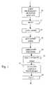
- FIG. 1is a simplified flowchart of an embodiment of an immersion photolithography using megasonic rinse
- FIG. 2is a simplified diagram of an embodiment of apparatus for performing immersion photolithography with megasonic rinse.
- the immersion exposure stepmay use deionized water or another suitable immersion exposure fluid in the space between the wafer and the lens.
- the photoresist materialmay leach into the immersion exposure liquid and cause heretofore unforeseen problems.
- the photoresist (also referred herein as resist) leached into the immersion exposure liquidmay adhere to the lens surface and adversely affect critical dimension uniformity.
- the resist that adhere to the lensmay not be easily removed and may require more frequent equipment maintenance and replacement.
- the leached resistmay comprise photo acid generator (PAG), which would release into the fluid when resist contact to immersion liquid.
- PAGphoto acid generator
- the leaching (PAG)is thought to be the main reason to cause the lens contamination.
- a photoresistis formed over the surface of the wafer substrate.
- the photoresistmay be a negative or positive resist and may be of a material now known or later developed for this purpose.
- the photoresistmay be a chemical amplification resist and may be a one- two- or multi-component resist system.
- the application of the photoresistmay be done with spin-coating or another suitable procedure.
- the waferPrior to the application of the photoresist, the wafer may be first processed to prepare it for the photolithography process. For example, the wafer may be cleaned, dried and/or coated with an adhesion-promoting material prior to the application of the photoresist.
- step 12the wafer is heated to generally drive off solvents, improve adhesion between the wafer and the photoresist, and anneal away stress that was introduced during the spin process.
- Step 12is commonly called the soft bake process, and the wafer is generally heated to about 90 to about 140° C., for example.
- the wafermay be heated for about 30 to about 200 seconds, for example. Thereafter, the wafer is allowed to cool down in step 14 .
- the waferis subjected to a megasonic rinse.
- Megasonic rinseis the use of an oscillating or pulsating liquid at frequencies ranging from about 10 to about 1000 KHz to rinse the wafer.
- the waferis immersed in a megasonic-energized liquid bath contained in a tank or subjected to a spray nozzle dispensing the liquid.
- the megasonic rinse liquidmay comprise generally deionized water and may additionally include a surfactant, a polymer and/or a buffer, for example.
- An example of suitable surfactantsincludes perflurooctanesulfonate (PFOS); an example of suitable polymer includes C3F8; and an example of suitable buffers includes phosphate.
- PFOSperflurooctanesulfonate
- suitable polymerincludes C3F8
- suitable buffersincludes phosphate.
- the surfactantmay be an ionic or anionic surfactant now known or later developed.
- One or more megasonic transducersmay be used to generate the oscillating energy in the rinse liquid.
- the megasonic rinse stepis operable to remove water-soluble molecules in the resist material to prevent leaching during immersion exposure.
- the megasonic rinse stepis operable to remove the gas in the resist material.
- the megasonic rinseis also operable to introduce water molecules inside the resist to increase the hydrophilic properties of the resist. The increased hydrophilic property may prevent the formation of micro-bubbles during alignment stage movement, exposure and other pre-exposure equipment activities. Therefore, the megasonic rinse step is operable to remove potential leaching molecules and fill air pockets in the resist that will contaminate the immersion exposure liquid.
- the megasonic rinse time durationmay range between about 5 seconds to about ten minutes, for example.
- the rinse liquidis dispensed onto the wafer or fed to an immersion bath and drained.
- the megasonic rinsemay be performed in the same chamber that the immersion exposure is performed, such as shown in FIG. 2 .
- Apparatus 30includes projection optics 32 that is operable to direct radiation onto the wafer 34 .
- One or more megasonic transducers 36may be turned on for the megasonic rinse step and then off during the immersion exposure step.
- the megasonic rinse solutions and immersion exposure liquidsmay be introduced to the interface 38 between the wafer 34 and the optical lens via an inlet 40 and drained via an outlet 42 .
- the inlet 40may comprise a spray nozzle.
- a megasonic energy generatoris coupled to the spray nozzle.
- the wafer 34rests on a wafer stage 44 which may comprise a vacuum chuck to hold the wafer in place.
- the wafer stageis operable to move or rotate according to the desired rinse and scanning motion.
- the megasonic rinse stepmay be followed by one or more additional deionized water rinse steps which may also be performed in apparatus 30 .
- the wafermay be transferred to a tank coupled to a megasonic energy generator for the megasonic rinse step.
- the immersion solutionis energized and agitated by the energy generator to rinse the wafer.
- the immersion exposure stepis performed.
- the wafer and resistis immersed in an immersion exposure liquid and exposed to a radiation source through a mask.
- the radiation sourcemay be an ultraviolet light source, for example a krypton fluoride (KrF, 248 nm), argon fluoride (ArF, 193 nm), or F 2 (157 nm) excimer laser.
- the waferis exposed to the radiation for a predetermined amount of time is dependent on the type of photoresist used, the intensity of the ultraviolet light source, and/or other factors.
- the exposure timemay last from about 0.2 seconds to about 30 seconds, for example.
- the exposed photo resistis then heated for a post-exposure bake.
- This steplets the exposed photo acid react with the polymer and make the polymer dissolution.
- the wafermay be heated to a temperature of about 85 to about 150° C., for example, for about 30 to about 200 seconds, for example.
- the exposed (positive) or unexposed (negative) photoresistis removed to leave the desired mask pattern.
- the waferis immersed in a developer liquid for a predetermined amount of time during which a portion of the photoresist is dissolved and removed.
- the wafermay be immersed in the developer solution for about 5 to about 60 seconds, for example.
- the composition of the developeris dependent on the composition of the photoresist.
- step 24the wafer is then heated for a post-developing hard bake. This step further removes solvents, improve adhesion, and increase the etch resistance of the resist.
- the wafermay be heated to a temperature of about 90 to about 130° C., for example, for about 30 to about 200 seconds, for example.
- the wafer with the patterned photoresistmay be used to form one or more layers of materials to form device features.
- the megasonic rinse step introduced prior to immersion exposureremoves resist molecules that are prone to leach into the immersion exposure liquid as well as fill in spaces that may lead to the formation of micro-bubbles during the exposure process. These contaminants in the immersion exposure liquid compromise the exposure process.
- the resist moleculesmay adhere to the lens and change the optical performance of the lens, the refractive index of the liquid and jeopardize critical dimension uniformity.
- the resist adhering to the lens and other hardwaremay also lead to additional equipment maintenance requirements.
- the formation of micro-bubblesalso would change the refractive index of the liquid and generate erroneous resist image.
Landscapes
- Physics & Mathematics (AREA)
- General Physics & Mathematics (AREA)
- Engineering & Computer Science (AREA)
- Condensed Matter Physics & Semiconductors (AREA)
- Manufacturing & Machinery (AREA)
- Computer Hardware Design (AREA)
- Microelectronics & Electronic Packaging (AREA)
- Power Engineering (AREA)
- Exposure Of Semiconductors, Excluding Electron Or Ion Beam Exposure (AREA)
- Exposure And Positioning Against Photoresist Photosensitive Materials (AREA)
- Photosensitive Polymer And Photoresist Processing (AREA)
- Cleaning Or Drying Semiconductors (AREA)
Abstract
Description
Claims (18)
Priority Applications (6)
| Application Number | Priority Date | Filing Date | Title |
|---|---|---|---|
| US10/995,653US7732123B2 (en) | 2004-11-23 | 2004-11-23 | Immersion photolithography with megasonic rinse |
| TW094118265ATWI267908B (en) | 2004-11-23 | 2005-06-02 | Immersion photolithography with megasonic rinse |
| CNB2005100753346ACN100432841C (en) | 2004-11-23 | 2005-06-10 | Immersion lithography method and apparatus |
| NL1030480ANL1030480C2 (en) | 2004-11-23 | 2005-11-21 | Immersion photolithography with megasonic wash. |
| JP2005337792AJP4571067B2 (en) | 2004-11-23 | 2005-11-22 | Immersion photolithography using megasonic ultrasonic rinse |
| KR1020050112164AKR100733994B1 (en) | 2004-11-23 | 2005-11-23 | Immersion photolithography with megasonic rinse |
Applications Claiming Priority (1)
| Application Number | Priority Date | Filing Date | Title |
|---|---|---|---|
| US10/995,653US7732123B2 (en) | 2004-11-23 | 2004-11-23 | Immersion photolithography with megasonic rinse |
Publications (2)
| Publication Number | Publication Date |
|---|---|
| US20060110689A1 US20060110689A1 (en) | 2006-05-25 |
| US7732123B2true US7732123B2 (en) | 2010-06-08 |
Family
ID=36461320
Family Applications (1)
| Application Number | Title | Priority Date | Filing Date |
|---|---|---|---|
| US10/995,653Expired - Fee RelatedUS7732123B2 (en) | 2004-11-23 | 2004-11-23 | Immersion photolithography with megasonic rinse |
Country Status (6)
| Country | Link |
|---|---|
| US (1) | US7732123B2 (en) |
| JP (1) | JP4571067B2 (en) |
| KR (1) | KR100733994B1 (en) |
| CN (1) | CN100432841C (en) |
| NL (1) | NL1030480C2 (en) |
| TW (1) | TWI267908B (en) |
Families Citing this family (16)
| Publication number | Priority date | Publication date | Assignee | Title |
|---|---|---|---|---|
| WO2005124833A1 (en)* | 2004-06-21 | 2005-12-29 | Nikon Corporation | Exposure device, exposure device member cleaning method, exposure device maintenance method, maintenance device, and device manufacturing method |
| CN101044594B (en)* | 2004-10-26 | 2010-05-12 | 株式会社尼康 | Substrate processing method, exposure apparatus, and device manufacturing method |
| US20070242248A1 (en)* | 2004-10-26 | 2007-10-18 | Nikon Corporation | Substrate processing method, exposure apparatus, and method for producing device |
| JP4784513B2 (en)* | 2004-12-06 | 2011-10-05 | 株式会社ニコン | Maintenance method, maintenance equipment, exposure apparatus, and device manufacturing method |
| US7880860B2 (en) | 2004-12-20 | 2011-02-01 | Asml Netherlands B.V. | Lithographic apparatus and device manufacturing method |
| US20060194142A1 (en)* | 2005-02-25 | 2006-08-31 | Benjamin Szu-Min Lin | Immersion lithography without using a topcoat |
| US20060250588A1 (en)* | 2005-05-03 | 2006-11-09 | Stefan Brandl | Immersion exposure tool cleaning system and method |
| KR20080031376A (en)* | 2005-07-11 | 2008-04-08 | 가부시키가이샤 니콘 | Exposure apparatus and device manufacturing method |
| TW200805000A (en)* | 2006-05-18 | 2008-01-16 | Nikon Corp | Exposure method and apparatus, maintenance method and device manufacturing method |
| CN102109773A (en)* | 2006-05-22 | 2011-06-29 | 株式会社尼康 | Exposure method, exposure apparatus, and maintenance method |
| EP2034515A4 (en)* | 2006-05-23 | 2012-01-18 | Nikon Corp | Maintenance method, exposure method and apparatus, and device manufacturing method |
| EP2043134A4 (en)* | 2006-06-30 | 2012-01-25 | Nikon Corp | Maintenance method, exposure method and apparatus and device manufacturing method |
| US7800731B2 (en)* | 2006-11-03 | 2010-09-21 | Taiwan Semiconductor Manufacturing Company, Ltd. | Method and apparatus for removing particles in immersion lithography |
| US20110094546A1 (en)* | 2009-10-23 | 2011-04-28 | John Valcore | System and method for wafer carrier vibration reduction |
| NL2006272A (en)* | 2010-05-04 | 2011-11-07 | Asml Netherlands Bv | A fluid handling structure, a lithographic apparatus and a device manufacturing method. |
| EP4062233A1 (en) | 2019-11-18 | 2022-09-28 | ASML Netherlands B.V. | A fluid handling system, method and lithographic apparatus |
Citations (23)
| Publication number | Priority date | Publication date | Assignee | Title |
|---|---|---|---|---|
| US4480910A (en) | 1981-03-18 | 1984-11-06 | Hitachi, Ltd. | Pattern forming apparatus |
| US4509852A (en) | 1980-10-06 | 1985-04-09 | Werner Tabarelli | Apparatus for the photolithographic manufacture of integrated circuit elements |
| JPH06168866A (en) | 1992-11-27 | 1994-06-14 | Canon Inc | Immersion projection exposure system |
| JPH0739833A (en) | 1993-07-29 | 1995-02-10 | Matsushita Electric Ind Co Ltd | Cleaning equipment |
| US5783790A (en) | 1995-11-30 | 1998-07-21 | Organo Corporation | Wet treatment method |
| US5900354A (en) | 1997-07-03 | 1999-05-04 | Batchelder; John Samuel | Method for optical inspection and lithography |
| US5911837A (en) | 1993-07-16 | 1999-06-15 | Legacy Systems, Inc. | Process for treatment of semiconductor wafers in a fluid |
| US20010047810A1 (en)* | 1999-06-29 | 2001-12-06 | Jeff Farber | High rpm megasonic cleaning |
| US6496257B1 (en) | 1997-11-21 | 2002-12-17 | Nikon Corporation | Projection exposure apparatus and method |
| US6517665B1 (en)* | 2000-01-25 | 2003-02-11 | Sandia National Laboratories | Liga developer apparatus system |
| US20030068837A1 (en)* | 2001-08-31 | 2003-04-10 | John Klocke | Apparatus and method for deposition of an electrophoretic emulsion |
| US6562550B2 (en)* | 2000-04-14 | 2003-05-13 | Tdk Corporation | Preparation of optical disk master |
| JP2003289060A (en) | 2002-01-28 | 2003-10-10 | Mitsubishi Chemicals Corp | Cleaning liquid and cleaning method for substrate for semiconductor device |
| US20030234029A1 (en)* | 2001-07-16 | 2003-12-25 | Semitool, Inc. | Cleaning and drying a substrate |
| JP2004078217A (en) | 2002-08-12 | 2004-03-11 | Air Products & Chemicals Inc | Method of reducing defects in manufacturing semiconductor device, and processing solution |
| US20040121617A1 (en) | 2002-10-11 | 2004-06-24 | Kenji Kawano | Method of processing a substrate, heating apparatus, and method of forming a pattern |
| US6754980B2 (en) | 2001-06-12 | 2004-06-29 | Goldfinger Technologies, Llc | Megasonic cleaner and dryer |
| US20040180299A1 (en)* | 2003-03-11 | 2004-09-16 | Rolland Jason P. | Immersion lithography methods using carbon dioxide |
| US20050024609A1 (en)* | 2003-06-11 | 2005-02-03 | Asml Netherlands B.V. | Lithographic apparatus and device manufacturing method |
| US20050048223A1 (en)* | 2003-09-02 | 2005-03-03 | Pawloski Adam R. | Method and apparatus for elimination of bubbles in immersion medium in immersion lithography systems |
| US20060103818A1 (en)* | 2004-11-18 | 2006-05-18 | International Business Machines Corporation | Method and apparatus for cleaning a semiconductor substrate in an immersion lithography system |
| US7056646B1 (en)* | 2003-10-01 | 2006-06-06 | Advanced Micro Devices, Inc. | Use of base developers as immersion lithography fluid |
| US7110081B2 (en)* | 2002-11-12 | 2006-09-19 | Asml Netherlands B.V. | Lithographic apparatus and device manufacturing method |
Family Cites Families (6)
| Publication number | Priority date | Publication date | Assignee | Title |
|---|---|---|---|---|
| JPH06124873A (en)* | 1992-10-09 | 1994-05-06 | Canon Inc | Immersion projection exposure system |
| CN1170208C (en)* | 2001-06-21 | 2004-10-06 | 中国科学院长春光学精密机械与物理研究所 | Separation Exposure Process Method Using Ordinary Ultraviolet Light for Deep Layer Lithography |
| KR20040058966A (en)* | 2002-12-27 | 2004-07-05 | 주식회사 하이닉스반도체 | Immersion lithography method |
| CN101825847B (en)* | 2003-04-11 | 2013-10-16 | 株式会社尼康 | Cleanup method for optics in immersion lithography |
| KR20050113462A (en)* | 2004-05-29 | 2005-12-02 | 삼성전자주식회사 | Water immersion lithography equipment |
| JP2006049757A (en)* | 2004-08-09 | 2006-02-16 | Tokyo Electron Ltd | Substrate processing method |
- 2004
- 2004-11-23USUS10/995,653patent/US7732123B2/ennot_activeExpired - Fee Related
- 2005
- 2005-06-02TWTW094118265Apatent/TWI267908B/ennot_activeIP Right Cessation
- 2005-06-10CNCNB2005100753346Apatent/CN100432841C/ennot_activeExpired - Fee Related
- 2005-11-21NLNL1030480Apatent/NL1030480C2/enactiveSearch and Examination
- 2005-11-22JPJP2005337792Apatent/JP4571067B2/enactiveActive
- 2005-11-23KRKR1020050112164Apatent/KR100733994B1/enactiveActive
Patent Citations (24)
| Publication number | Priority date | Publication date | Assignee | Title |
|---|---|---|---|---|
| US4509852A (en) | 1980-10-06 | 1985-04-09 | Werner Tabarelli | Apparatus for the photolithographic manufacture of integrated circuit elements |
| US4480910A (en) | 1981-03-18 | 1984-11-06 | Hitachi, Ltd. | Pattern forming apparatus |
| JPH06168866A (en) | 1992-11-27 | 1994-06-14 | Canon Inc | Immersion projection exposure system |
| US5911837A (en) | 1993-07-16 | 1999-06-15 | Legacy Systems, Inc. | Process for treatment of semiconductor wafers in a fluid |
| JPH0739833A (en) | 1993-07-29 | 1995-02-10 | Matsushita Electric Ind Co Ltd | Cleaning equipment |
| US5783790A (en) | 1995-11-30 | 1998-07-21 | Organo Corporation | Wet treatment method |
| US5900354A (en) | 1997-07-03 | 1999-05-04 | Batchelder; John Samuel | Method for optical inspection and lithography |
| US6496257B1 (en) | 1997-11-21 | 2002-12-17 | Nikon Corporation | Projection exposure apparatus and method |
| US20010047810A1 (en)* | 1999-06-29 | 2001-12-06 | Jeff Farber | High rpm megasonic cleaning |
| US6517665B1 (en)* | 2000-01-25 | 2003-02-11 | Sandia National Laboratories | Liga developer apparatus system |
| US6562550B2 (en)* | 2000-04-14 | 2003-05-13 | Tdk Corporation | Preparation of optical disk master |
| US6754980B2 (en) | 2001-06-12 | 2004-06-29 | Goldfinger Technologies, Llc | Megasonic cleaner and dryer |
| US20030234029A1 (en)* | 2001-07-16 | 2003-12-25 | Semitool, Inc. | Cleaning and drying a substrate |
| US20030068837A1 (en)* | 2001-08-31 | 2003-04-10 | John Klocke | Apparatus and method for deposition of an electrophoretic emulsion |
| JP2003289060A (en) | 2002-01-28 | 2003-10-10 | Mitsubishi Chemicals Corp | Cleaning liquid and cleaning method for substrate for semiconductor device |
| JP2004078217A (en) | 2002-08-12 | 2004-03-11 | Air Products & Chemicals Inc | Method of reducing defects in manufacturing semiconductor device, and processing solution |
| US20040121617A1 (en) | 2002-10-11 | 2004-06-24 | Kenji Kawano | Method of processing a substrate, heating apparatus, and method of forming a pattern |
| US7110081B2 (en)* | 2002-11-12 | 2006-09-19 | Asml Netherlands B.V. | Lithographic apparatus and device manufacturing method |
| US20040180299A1 (en)* | 2003-03-11 | 2004-09-16 | Rolland Jason P. | Immersion lithography methods using carbon dioxide |
| US20050024609A1 (en)* | 2003-06-11 | 2005-02-03 | Asml Netherlands B.V. | Lithographic apparatus and device manufacturing method |
| US20050048223A1 (en)* | 2003-09-02 | 2005-03-03 | Pawloski Adam R. | Method and apparatus for elimination of bubbles in immersion medium in immersion lithography systems |
| US7056646B1 (en)* | 2003-10-01 | 2006-06-06 | Advanced Micro Devices, Inc. | Use of base developers as immersion lithography fluid |
| US20060103818A1 (en)* | 2004-11-18 | 2006-05-18 | International Business Machines Corporation | Method and apparatus for cleaning a semiconductor substrate in an immersion lithography system |
| JP2006148093A (en) | 2004-11-18 | 2006-06-08 | Internatl Business Mach Corp <Ibm> | Method and equipment for cleaning semiconductor substrate in immersion lithography system |
Non-Patent Citations (2)
| Title |
|---|
| Chinese Patent Office, Office Action, Apr. 18, 2004, 5 pages, Application No. 2005100753346. |
| Decision of Refusal from the Japanese Patent Office for JP2005-337792 dated Sep. 15, 2009, 4 pages (with English translation). |
Also Published As
| Publication number | Publication date |
|---|---|
| JP4571067B2 (en) | 2010-10-27 |
| TWI267908B (en) | 2006-12-01 |
| NL1030480A1 (en) | 2006-05-24 |
| CN1779573A (en) | 2006-05-31 |
| KR20060057517A (en) | 2006-05-26 |
| CN100432841C (en) | 2008-11-12 |
| JP2006148133A (en) | 2006-06-08 |
| KR100733994B1 (en) | 2007-06-29 |
| TW200618058A (en) | 2006-06-01 |
| NL1030480C2 (en) | 2008-04-25 |
| US20060110689A1 (en) | 2006-05-25 |
Similar Documents
| Publication | Publication Date | Title |
|---|---|---|
| US7732123B2 (en) | Immersion photolithography with megasonic rinse | |
| JP4005879B2 (en) | Development method, substrate processing method, and substrate processing apparatus | |
| JP4476979B2 (en) | Method for forming immersion lithography of semiconductor substrate and method for processing semiconductor wafer | |
| CN100474119C (en) | Resist pattern forming method and semiconductor device manufacturing method | |
| KR100801161B1 (en) | Methods and systems for inhibiting immersion lithography defect formation | |
| US8084194B2 (en) | Substrate edge treatment for coater/developer | |
| KR20060130237A (en) | Coating and developing apparatus and coating and developing method | |
| US8027017B2 (en) | Substrate treating apparatus and exposing apparatus for cleaning a chuck cleaning tool with treating bath | |
| JP2017147328A (en) | Developing unit, substrate processing apparatus, developing method, and substrate processing method | |
| JP4531726B2 (en) | Method for forming miniaturized resist pattern | |
| TWI438562B (en) | Photomask manufacturing method, pattern transfer method, processing apparatus for a photomask substrate, and thin film patterning method | |
| JP4564186B2 (en) | Pattern formation method | |
| KR101216797B1 (en) | Method of processing substrate, method of manufacturing euv mask and euv mask | |
| US20070093067A1 (en) | Wafer edge cleaning process | |
| JP2012256726A (en) | Rework method for resist film, manufacturing method for semiconductor device, and substrate processing system | |
| JP3475314B2 (en) | Method of forming resist pattern | |
| CN109991820B (en) | Device and method for removing residual water drops after immersion exposure | |
| JPH07335519A (en) | Pattern formation method | |
| JP3861851B2 (en) | Resist pattern forming method and semiconductor device manufacturing method | |
| JP5012393B2 (en) | Coating, developing device, coating, developing method and storage medium | |
| US20240248413A1 (en) | Substrate treatment method and substrate treatment apparatus | |
| JP4527037B2 (en) | Substrate development processing method and substrate development processing apparatus | |
| CN110308624B (en) | A kind of laser lithography three-dimensional micro-nano device supercritical fluid developing device and method | |
| KR20060025244A (en) | Photoresist developing device with decontamination function of cleaning nozzle | |
| JPH11154634A (en) | Manufacture of semiconductor device and device therefor |
Legal Events
| Date | Code | Title | Description |
|---|---|---|---|
| AS | Assignment | Owner name:TAIWAN SEMICONDUCTOR MANUFACTURING COMPANY, LTD., Free format text:ASSIGNMENT OF ASSIGNORS INTEREST;ASSIGNOR:CHANG, CHING-YU;REEL/FRAME:015559/0365 Effective date:20041129 Owner name:TAIWAN SEMICONDUCTOR MANUFACTURING COMPANY, LTD.,T Free format text:ASSIGNMENT OF ASSIGNORS INTEREST;ASSIGNOR:CHANG, CHING-YU;REEL/FRAME:015559/0365 Effective date:20041129 | |
| STCF | Information on status: patent grant | Free format text:PATENTED CASE | |
| FPAY | Fee payment | Year of fee payment:4 | |
| MAFP | Maintenance fee payment | Free format text:PAYMENT OF MAINTENANCE FEE, 8TH YEAR, LARGE ENTITY (ORIGINAL EVENT CODE: M1552) Year of fee payment:8 | |
| FEPP | Fee payment procedure | Free format text:MAINTENANCE FEE REMINDER MAILED (ORIGINAL EVENT CODE: REM.); ENTITY STATUS OF PATENT OWNER: LARGE ENTITY | |
| LAPS | Lapse for failure to pay maintenance fees | Free format text:PATENT EXPIRED FOR FAILURE TO PAY MAINTENANCE FEES (ORIGINAL EVENT CODE: EXP.); ENTITY STATUS OF PATENT OWNER: LARGE ENTITY | |
| STCH | Information on status: patent discontinuation | Free format text:PATENT EXPIRED DUE TO NONPAYMENT OF MAINTENANCE FEES UNDER 37 CFR 1.362 | |
| FP | Lapsed due to failure to pay maintenance fee | Effective date:20220608 |