US7729601B1 - Shutter for autofocus - Google Patents
Shutter for autofocusDownload PDFInfo
- Publication number
- US7729601B1 US7729601B1US11/849,049US84904907AUS7729601B1US 7729601 B1US7729601 B1US 7729601B1US 84904907 AUS84904907 AUS 84904907AUS 7729601 B1US7729601 B1US 7729601B1
- Authority
- US
- United States
- Prior art keywords
- image
- lens
- image data
- autofocus
- camera
- Prior art date
- Legal status (The legal status is an assumption and is not a legal conclusion. Google has not performed a legal analysis and makes no representation as to the accuracy of the status listed.)
- Active, expires
Links
Images


Classifications
- G—PHYSICS
- G03—PHOTOGRAPHY; CINEMATOGRAPHY; ANALOGOUS TECHNIQUES USING WAVES OTHER THAN OPTICAL WAVES; ELECTROGRAPHY; HOLOGRAPHY
- G03B—APPARATUS OR ARRANGEMENTS FOR TAKING PHOTOGRAPHS OR FOR PROJECTING OR VIEWING THEM; APPARATUS OR ARRANGEMENTS EMPLOYING ANALOGOUS TECHNIQUES USING WAVES OTHER THAN OPTICAL WAVES; ACCESSORIES THEREFOR
- G03B13/00—Viewfinders; Focusing aids for cameras; Means for focusing for cameras; Autofocus systems for cameras
- G03B13/32—Means for focusing
- G03B13/34—Power focusing
- G03B13/36—Autofocus systems
- G—PHYSICS
- G02—OPTICS
- G02B—OPTICAL ELEMENTS, SYSTEMS OR APPARATUS
- G02B13/00—Optical objectives specially designed for the purposes specified below
- G02B13/001—Miniaturised objectives for electronic devices, e.g. portable telephones, webcams, PDAs, small digital cameras
- G—PHYSICS
- G02—OPTICS
- G02B—OPTICAL ELEMENTS, SYSTEMS OR APPARATUS
- G02B7/00—Mountings, adjusting means, or light-tight connections, for optical elements
- G02B7/02—Mountings, adjusting means, or light-tight connections, for optical elements for lenses
- G02B7/04—Mountings, adjusting means, or light-tight connections, for optical elements for lenses with mechanism for focusing or varying magnification
- G02B7/08—Mountings, adjusting means, or light-tight connections, for optical elements for lenses with mechanism for focusing or varying magnification adapted to co-operate with a remote control mechanism
- G—PHYSICS
- G02—OPTICS
- G02B—OPTICAL ELEMENTS, SYSTEMS OR APPARATUS
- G02B7/00—Mountings, adjusting means, or light-tight connections, for optical elements
- G02B7/28—Systems for automatic generation of focusing signals
- H—ELECTRICITY
- H04—ELECTRIC COMMUNICATION TECHNIQUE
- H04N—PICTORIAL COMMUNICATION, e.g. TELEVISION
- H04N23/00—Cameras or camera modules comprising electronic image sensors; Control thereof
- H04N23/60—Control of cameras or camera modules
- H04N23/67—Focus control based on electronic image sensor signals
- H04N23/676—Bracketing for image capture at varying focusing conditions
Definitions
- This inventiongenerally relates to miniature cameras.
- Miniature camerasare currently available with many electronic devices, such as cellular telephones, laptop computers, personal digital assistants (PDAs), and the like. Miniature cameras are also available as stand-alone devices for applications such as security and surveillance.
- PDAspersonal digital assistants
- the methodcan comprise moving a lens and reading out first image data associated with a plurality of image pixels during a first low light interval, modifying one or more camera parameters to provide autofocus image light received at a detection system during an autofocus light interval, acquiring second image data associated with the plurality of image pixels during the autofocus light interval modifying at least one of the one or more camera parameters to substantially reduce image light received at the detection system during a second low light interval, reading out the second image data during the second low light interval, and analyzing at least the first image data and the second image data to determine a focus position of the lens.
- the methodcan comprise performing autofocus and performing image acquisition. At least one camera parameter is different during autofocus and image acquisition.
- FIG. 1is a timing diagram for an existing autofocus system
- FIG. 2is a timing diagram for an autofocus system, according to some embodiments.
- FIG. 3is a schematic diagram of a camera system, according to some embodiments.
- FIG. 4is a schematic diagram of a camera system and subject, according to some embodiments.
- an autofocus (AF) systemimplements a contrast AF process.
- the lensis moved to various incremental positions at different distances from an image sensor, and the best focus position is determined based on image data acquired at different lens positions.
- the image sensorcaptures an image at each incremental position while the lens is momentarily stationary.
- a sharpness filtermay be applied to each image to provide an associated sharpness score for each image.
- the lens position associated with the highest sharpness scoremay then be used for capturing in-focus images.
- CMOS imaging sensorsmay not be optimal.
- the acquired imagemay be blurred. This can be a particular problem with cameras using CMOS imaging sensors.
- an electronic rolling shutterIn a CMOS imaging sensor, an electronic rolling shutter (ERS) is used.
- ERSelectronic rolling shutter
- image data for each row in the imageis read out in sequence, so that image data for different rows is obtained at different times.
- the lens, camera, and/or image subject(s)move during the exposure time, the image is blurred, making the AF analysis inaccurate.
- FIG. 1shows timing diagram for an example of an existing AF process for a camera implementing ERS.
- the detectormay include a CMOS imaging sensor with an array (rows and columns) of image pixels.
- acquisition of image datais initiated in response to a Vertical Synch signal or Frame_valid signal.
- t 1sequential readout of the pixels of each of the rows of the detector is initiated.
- FIG. 1illustrates, although the integration time for each row is the same, the exposure for different rows starts and ends at a different time. Thus, movement may introduce blur into the acquired image data.
- the readout of all rowsis complete, and lens movement is initiated.
- the lensis in its next position, and image data acquisition is sequentially initiated in each of the rows in response to an ERS reset signal in a manner like that at t 0 .
- readout of the rowsis initiated in response to read out signals in a manner like that at t 1 .
- the vertical blanking time t 4 -t 2includes the time for lens movement, as well as the integration time for data acquisition.
- Relatively long vertical blanking timecan be a problem not only for systems incorporating ERS, but also systems using global electronic shuttering or global physical shuttering.
- global physical shutteringa physical shutter may be used to alternately block and transmit light, so that the image light for all pixels is received during the same time period.
- an analog memorymay be used for each pixel so that the image light for all pixels is received during the same time period.
- the vertical blanking timeis limited by the time needed to move the lens from one position to another and to settle at the new position.
- an actuatorrapidly accelerates the lens from the starting position toward the target position, then rapidly decelerates once the lens is near the target position. This may induce some oscillation about the target position.
- the lensneeds to be given time to settle prior to obtaining image date for the AF determination.
- the systems and techniques hereinmay provide a number of advantages over existing systems.
- First, the vertical blanking time and data acquisition timemay be significantly reduced.
- Second, the acquired data for all of the image pixelscorresponds to the same time interval, even if ERS is used.
- FIG. 2shows a timing diagram for an autofocus system, according to some embodiments.
- FIG. 3shows a schematic diagram of a camera system 300 that may be used to implement AF according to the timing diagram of FIG. 2 .
- Camera system 300includes a physical shutter 310 positioned on an actuator 320 .
- System 300further includes a lens 330 positioned on an actuator 340 .
- Light transmitted into the camera through shutter 310 and lens 330is incident on a detection system 350 including an imaging sensor such as a CCD or CMOS imaging sensor.
- System 300includes a controller 360 .
- controller 360receives image information from detection system 350 , and performs AF analysis to determine a best focus position based on image information corresponding to a plurality of positions of lens 330 .
- Controller 360also controls actuators 320 and 340 .
- the functions of controller 360may be performed by one or more modules in addition to the illustrated module, and controller 360 may be integrated in system 300 in a number of ways.
- a low light intervalis initiated. This may be accomplished in a number of ways.
- shutter 310may be positioned in front of the camera aperture to substantially block light from lens 330 and detection system 350 .
- the cameramay include a light source such as a flash strobe with “on” and “off” states.
- the low light intervalmay be initiated by switching from the on state to the off state.
- the low light intervalmay be initiated using electronic shuttering.
- lens 330may be moved from a first position to a second different position in response to receiving a control signal from controller 360 at actuator 340 .
- lens 330reaches the second position prior to the end of the low light interval, so that any oscillation of the lens that occurs does not affect the light acquired for the autofocus operation.
- the low light intervalends at t 1 .
- an auto-focus light intervalis initiated.
- imaging informationis acquired for all pixels. That is, all pixels are exposed at the same time, and for the same length of time.
- a second low light intervalis initiated, and lens 330 is moved to a different position.
- a second AF intervalis initiated at time t 3 .
- image informationmay be used to determine the best focus position of lens 330 .
- AF processing instructionsmay be stored in a memory in, for example, controller 360 and may be executed by a processor included in controller 360 .
- the frame ratemay be increased, but blurring due to movement of lens 330 , camera system 300 , and/or object(s) in the camera view may be substantially decreased.
- image acquisitionimage information obtained at the imaging sensor included in detection system 300 may be digitally amplified with an imaging gain G I to obtain a particular signal to noise ratio.
- G Igenerally depends on parameters such as the light level, exposure length, and the like.
- the gaincan be increased to a larger value G AF during the AF process.
- the noisemay increase due to larger gain, an accurate sharpness determination may be still be obtained.
- a flashmay be used to increase the luminance at the detector during the AF process, even when a flash would not provide the optimum image date during image acquisition.
- the movement of lens 330may be effectively hidden from the user. That is, although image information for AF may be obtained at a number of positions, the positioning may not be reflected in a display to a user.
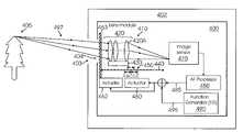
- FIG. 4illustrates a block diagram of a camera 400 with an adjustable focus in accordance with an embodiment of the invention.
- Camera 400may be implemented, for example, as a digital still camera or a digital video camera.
- camera 400may be implemented as a miniature camera that is part of a personal electronic device 402 such as a portable computer, a laptop computer, a notebook computer, a pocket personal computer (pocket PC), a personal digital assistant (PDA), a mobile telephone, a mobile security system, a fixed security system, or other device.
- Device 402 and camera 400include apertures 403 and 404 , respectively, which may receive light 497 reflected from an external object 405 .
- camera 400includes a lens module 410 , an actuator 460 , an image sensor 470 , an automatic focus (AF) processor 480 , and a function generator 490 .
- Lens module 410may include a plurality of lenses 420 secured relative to a stage 430 .
- Lens module 410may further include a lens barrel (not shown) for holding lenses 420 and a lens mount (not shown) for securing lenses 410 and/or the lens barrel to stage 430 .
- one or more of lenses 420may have a diameter in the range of about 10 microns to about 20 microns.
- Actuator 460may be in electrical, mechanical, and/or electro-magnetic communication (not shown) with stage 430 for controlling the position of stage 430 .
- actuator 460may be implemented in accordance with any appropriate mechanism for providing controlled movements on a scale appropriate for personal electronic device 402 .
- actuator 460may be implemented as a Lorentz motor, a micro-electro-mechanical systems (MEMS) device, or other appropriate apparatus.
- MEMSmicro-electro-mechanical systems
- Stage 430may be translated toward or away from image sensor 470 by actuator 460 along an axis 440 .
- a desired one of lenses 420may be selectively positioned at any of a plurality of positions 450 along axis 440 by translating stage 430 (and thereby translating lenses 420 ) to a desired one of positions 450 .
- a center of a lens 420 Ais aligned with position 450 B along axis 440 .
- positions 450may be spaced approximately 20 microns apart.
- Image sensor 470may be configured to capture digital images of object 405 from light 497 passing through lenses 420 .
- Image sensor 470may be implemented using any appropriate technology for capturing digital images such as, for example, a charge-coupled device (CCD) or complimentary metal-oxide semiconductor (CMOS) device. Images of object 480 captured by image sensor 470 can be provided to AF processor 460 .
- CCDcharge-coupled device
- CMOScomplimentary metal-oxide semiconductor
- AF processor 480may be configured with appropriate hardware and/or software to perform various operations as further described herein. AF processor 480 may provide control signals 485 to actuator 460 for controlling the movement of stage 430 and lenses 420 . Function generator 490 may be configured with appropriate hardware and/or software to provide control signals 495 to actuator 460 which may be combined with control signals 485 as illustrated in FIG. 4 . AF processor 480 may also provide control signals to an actuator 462 to move a shutter 463 to alternately block and transmit light 497 .
- the above described techniques and their variationsmay be implemented at least partially as computer software instructions. Such instructions may be stored on one or more machine-readable storage media or devices and are executed by, e.g., one or more computer processors, or cause the machine, to perform the described functions and operations.
Landscapes
- Physics & Mathematics (AREA)
- General Physics & Mathematics (AREA)
- Optics & Photonics (AREA)
- Engineering & Computer Science (AREA)
- Multimedia (AREA)
- Signal Processing (AREA)
- Studio Devices (AREA)
- Automatic Focus Adjustment (AREA)
Abstract
Description
Claims (5)
Priority Applications (1)
| Application Number | Priority Date | Filing Date | Title |
|---|---|---|---|
| US11/849,049US7729601B1 (en) | 2007-08-31 | 2007-08-31 | Shutter for autofocus |
Applications Claiming Priority (1)
| Application Number | Priority Date | Filing Date | Title |
|---|---|---|---|
| US11/849,049US7729601B1 (en) | 2007-08-31 | 2007-08-31 | Shutter for autofocus |
Publications (1)
| Publication Number | Publication Date |
|---|---|
| US7729601B1true US7729601B1 (en) | 2010-06-01 |
Family
ID=42200244
Family Applications (1)
| Application Number | Title | Priority Date | Filing Date |
|---|---|---|---|
| US11/849,049Active2028-07-21US7729601B1 (en) | 2007-08-31 | 2007-08-31 | Shutter for autofocus |
Country Status (1)
| Country | Link |
|---|---|
| US (1) | US7729601B1 (en) |
Cited By (8)
| Publication number | Priority date | Publication date | Assignee | Title |
|---|---|---|---|---|
| US20110226935A1 (en)* | 2008-09-19 | 2011-09-22 | National Univ. Corporation | Information-acquisition device and optical communication system |
| WO2012041892A1 (en) | 2010-09-28 | 2012-04-05 | DigitalOptics Corporation Europe Limited | Continuous autofocus based on face detection and tracking |
| WO2012062893A2 (en) | 2010-11-11 | 2012-05-18 | DigitalOptics Corporation Europe Limited | Object detection and recognition under out of focus conditions |
| US8659697B2 (en) | 2010-11-11 | 2014-02-25 | DigitalOptics Corporation Europe Limited | Rapid auto-focus using classifier chains, MEMS and/or multiple object focusing |
| WO2014072837A2 (en) | 2012-06-07 | 2014-05-15 | DigitalOptics Corporation Europe Limited | Mems fast focus camera module |
| CN105872356A (en)* | 2015-02-05 | 2016-08-17 | 奥林巴斯株式会社 | Imaging apparatus and imaging method |
| US9817206B2 (en) | 2012-03-10 | 2017-11-14 | Digitaloptics Corporation | MEMS auto focus miniature camera module with fixed and movable lens groups |
| US11082606B1 (en)* | 2018-09-11 | 2021-08-03 | Apple Inc. | Method and system for robust contrast based auto focus in low light |
Citations (3)
| Publication number | Priority date | Publication date | Assignee | Title |
|---|---|---|---|---|
| US7071986B2 (en)* | 2000-06-09 | 2006-07-04 | Minolta Co., Ltd. | Digital camera utilizing illumination from a flash light for focus detection and control |
| US20080062529A1 (en)* | 2004-09-30 | 2008-03-13 | Koninklijke Philips Electronics, N.V. | Controlllable Optical Lens |
| US20080095523A1 (en)* | 2006-10-18 | 2008-04-24 | Lynn Schilling-Benz | Lens array assisted focus detection |
- 2007
- 2007-08-31USUS11/849,049patent/US7729601B1/enactiveActive
Patent Citations (3)
| Publication number | Priority date | Publication date | Assignee | Title |
|---|---|---|---|---|
| US7071986B2 (en)* | 2000-06-09 | 2006-07-04 | Minolta Co., Ltd. | Digital camera utilizing illumination from a flash light for focus detection and control |
| US20080062529A1 (en)* | 2004-09-30 | 2008-03-13 | Koninklijke Philips Electronics, N.V. | Controlllable Optical Lens |
| US20080095523A1 (en)* | 2006-10-18 | 2008-04-24 | Lynn Schilling-Benz | Lens array assisted focus detection |
Cited By (14)
| Publication number | Priority date | Publication date | Assignee | Title |
|---|---|---|---|---|
| US20110226935A1 (en)* | 2008-09-19 | 2011-09-22 | National Univ. Corporation | Information-acquisition device and optical communication system |
| US8891978B2 (en)* | 2008-09-19 | 2014-11-18 | National University Corporation Shizuoka University | Information-acquisition device and optical communication system |
| WO2012041892A1 (en) | 2010-09-28 | 2012-04-05 | DigitalOptics Corporation Europe Limited | Continuous autofocus based on face detection and tracking |
| US8970770B2 (en) | 2010-09-28 | 2015-03-03 | Fotonation Limited | Continuous autofocus based on face detection and tracking |
| US8797448B2 (en) | 2010-11-11 | 2014-08-05 | DigitalOptics Corporation Europe Limited | Rapid auto-focus using classifier chains, MEMS and multiple object focusing |
| US8659697B2 (en) | 2010-11-11 | 2014-02-25 | DigitalOptics Corporation Europe Limited | Rapid auto-focus using classifier chains, MEMS and/or multiple object focusing |
| US8648959B2 (en) | 2010-11-11 | 2014-02-11 | DigitalOptics Corporation Europe Limited | Rapid auto-focus using classifier chains, MEMS and/or multiple object focusing |
| WO2012062893A2 (en) | 2010-11-11 | 2012-05-18 | DigitalOptics Corporation Europe Limited | Object detection and recognition under out of focus conditions |
| EP3007104A1 (en) | 2010-11-11 | 2016-04-13 | FotoNation Limited | Object detection and recognition under out of focus conditions |
| EP3236391A1 (en) | 2010-11-11 | 2017-10-25 | FotoNation Limited | Object detection and recognition under out of focus conditions |
| US9817206B2 (en) | 2012-03-10 | 2017-11-14 | Digitaloptics Corporation | MEMS auto focus miniature camera module with fixed and movable lens groups |
| WO2014072837A2 (en) | 2012-06-07 | 2014-05-15 | DigitalOptics Corporation Europe Limited | Mems fast focus camera module |
| CN105872356A (en)* | 2015-02-05 | 2016-08-17 | 奥林巴斯株式会社 | Imaging apparatus and imaging method |
| US11082606B1 (en)* | 2018-09-11 | 2021-08-03 | Apple Inc. | Method and system for robust contrast based auto focus in low light |
Similar Documents
| Publication | Publication Date | Title |
|---|---|---|
| US7729601B1 (en) | Shutter for autofocus | |
| US7693406B2 (en) | Image capturing apparatus, method of controlling the same, and storage medium | |
| JP4874668B2 (en) | Autofocus unit and camera | |
| JP5948492B2 (en) | Imaging apparatus and focus control method | |
| KR20160072687A (en) | Camera Module | |
| US10812704B2 (en) | Focus detection device, method and storage medium, for controlling image sensor operations | |
| JP2007116679A (en) | Imaging device with blur reduction system | |
| WO2014080673A1 (en) | Imaging device and exposure determination method | |
| WO2015118727A1 (en) | Image capture device and focus control method | |
| US20190243533A1 (en) | Display controller, control method thereof, and non-transitory computer readable medium | |
| US20050219386A1 (en) | Imaging device with burst zoom mode | |
| JP2018101055A (en) | Focus adjustment device, imaging device and focus adjustment method | |
| CN107255900B (en) | Control method of photographing device | |
| KR20240001131A (en) | Image alignment for computational photography | |
| CN102244727B (en) | Image pickup apparatus | |
| JP5086270B2 (en) | Imaging system with adjustable optics | |
| US9667878B2 (en) | Image capturing apparatus and control method for image capturing apparatus | |
| JP2008129371A (en) | Imaging device | |
| US20150168739A1 (en) | Image stabilizer, camera system, and imaging method | |
| CN113316928A (en) | Imaging element, imaging device, image data processing method, and program | |
| US10277796B2 (en) | Imaging control apparatus, imaging apparatus, and imaging control method | |
| JPWO2018168228A1 (en) | Image processing apparatus, image processing method, and image processing program | |
| JP2007057974A (en) | Photographing device | |
| JP5182395B2 (en) | Imaging apparatus, imaging method, and imaging program | |
| US10771675B2 (en) | Imaging control apparatus and imaging control method |
Legal Events
| Date | Code | Title | Description |
|---|---|---|---|
| AS | Assignment | Owner name:SIIMPEL CORPORATION,CALIFORNIA Free format text:ASSIGNMENT OF ASSIGNORS INTEREST;ASSIGNOR:TSAI, RICHARD;REEL/FRAME:019772/0568 Effective date:20070831 | |
| AS | Assignment | Owner name:SCALE VENTURE PARTNERS II, L.P., AS COLLATERAL AGE Free format text:PATENT SECURITY AGREEMENT;ASSIGNOR:SIIMPEL CORPORATION;REEL/FRAME:023519/0715 Effective date:20091112 | |
| AS | Assignment | Owner name:SCALE VENTURE PARTNERS II, L.P.,CALIFORNIA Free format text:PATENT SECURITY AGREEMENT;ASSIGNOR:SIIMPEL CORPORATION;REEL/FRAME:024170/0078 Effective date:20100330 Owner name:SCALE VENTURE PARTNERS II, L.P., CALIFORNIA Free format text:PATENT SECURITY AGREEMENT;ASSIGNOR:SIIMPEL CORPORATION;REEL/FRAME:024170/0078 Effective date:20100330 | |
| AS | Assignment | Owner name:SIIMPEL CORPORATION,CALIFORNIA Free format text:RELEASE BY SECURED PARTY;ASSIGNOR:SCALE VENTURE PARTNERS II, L.P.;REEL/FRAME:024351/0353 Effective date:20100505 Owner name:SIIMPEL CORPORATION, CALIFORNIA Free format text:RELEASE BY SECURED PARTY;ASSIGNOR:SCALE VENTURE PARTNERS II, L.P.;REEL/FRAME:024351/0353 Effective date:20100505 | |
| STCF | Information on status: patent grant | Free format text:PATENTED CASE | |
| AS | Assignment | Owner name:TESSERA MEMS TECHNOLOGIES, INC., CALIFORNIA Free format text:CHANGE OF NAME;ASSIGNOR:SIIMPEL CORPORATION;REEL/FRAME:025042/0294 Effective date:20100712 | |
| AS | Assignment | Owner name:DIGITALOPTICS CORPORATION MEMS, CALIFORNIA Free format text:CHANGE OF NAME;ASSIGNOR:TESSERA MEMS TECHNOLOGIES, INC.;REEL/FRAME:026794/0897 Effective date:20110630 | |
| FEPP | Fee payment procedure | Free format text:PAT HOLDER NO LONGER CLAIMS SMALL ENTITY STATUS, ENTITY STATUS SET TO UNDISCOUNTED (ORIGINAL EVENT CODE: STOL); ENTITY STATUS OF PATENT OWNER: LARGE ENTITY | |
| FPAY | Fee payment | Year of fee payment:4 | |
| AS | Assignment | Owner name:ROYAL BANK OF CANADA, AS COLLATERAL AGENT, CANADA Free format text:SECURITY INTEREST;ASSIGNORS:INVENSAS CORPORATION;TESSERA, INC.;TESSERA ADVANCED TECHNOLOGIES, INC.;AND OTHERS;REEL/FRAME:040797/0001 Effective date:20161201 | |
| MAFP | Maintenance fee payment | Free format text:PAYMENT OF MAINTENANCE FEE, 8TH YEAR, LARGE ENTITY (ORIGINAL EVENT CODE: M1552) Year of fee payment:8 | |
| AS | Assignment | Owner name:INVENSAS CORPORATION, CALIFORNIA Free format text:RELEASE BY SECURED PARTY;ASSIGNOR:ROYAL BANK OF CANADA;REEL/FRAME:052920/0001 Effective date:20200601 Owner name:DTS, INC., CALIFORNIA Free format text:RELEASE BY SECURED PARTY;ASSIGNOR:ROYAL BANK OF CANADA;REEL/FRAME:052920/0001 Effective date:20200601 Owner name:TESSERA, INC., CALIFORNIA Free format text:RELEASE BY SECURED PARTY;ASSIGNOR:ROYAL BANK OF CANADA;REEL/FRAME:052920/0001 Effective date:20200601 Owner name:TESSERA ADVANCED TECHNOLOGIES, INC, CALIFORNIA Free format text:RELEASE BY SECURED PARTY;ASSIGNOR:ROYAL BANK OF CANADA;REEL/FRAME:052920/0001 Effective date:20200601 Owner name:PHORUS, INC., CALIFORNIA Free format text:RELEASE BY SECURED PARTY;ASSIGNOR:ROYAL BANK OF CANADA;REEL/FRAME:052920/0001 Effective date:20200601 Owner name:IBIQUITY DIGITAL CORPORATION, MARYLAND Free format text:RELEASE BY SECURED PARTY;ASSIGNOR:ROYAL BANK OF CANADA;REEL/FRAME:052920/0001 Effective date:20200601 Owner name:DTS LLC, CALIFORNIA Free format text:RELEASE BY SECURED PARTY;ASSIGNOR:ROYAL BANK OF CANADA;REEL/FRAME:052920/0001 Effective date:20200601 Owner name:FOTONATION CORPORATION (F/K/A DIGITALOPTICS CORPORATION AND F/K/A DIGITALOPTICS CORPORATION MEMS), CALIFORNIA Free format text:RELEASE BY SECURED PARTY;ASSIGNOR:ROYAL BANK OF CANADA;REEL/FRAME:052920/0001 Effective date:20200601 Owner name:INVENSAS BONDING TECHNOLOGIES, INC. (F/K/A ZIPTRONIX, INC.), CALIFORNIA Free format text:RELEASE BY SECURED PARTY;ASSIGNOR:ROYAL BANK OF CANADA;REEL/FRAME:052920/0001 Effective date:20200601 | |
| MAFP | Maintenance fee payment | Free format text:PAYMENT OF MAINTENANCE FEE, 12TH YEAR, LARGE ENTITY (ORIGINAL EVENT CODE: M1553); ENTITY STATUS OF PATENT OWNER: LARGE ENTITY Year of fee payment:12 | |
| AS | Assignment | Owner name:BANK OF AMERICA, N.A., AS COLLATERAL AGENT, NORTH CAROLINA Free format text:SECURITY INTEREST;ASSIGNORS:ADEIA GUIDES INC.;ADEIA IMAGING LLC;ADEIA MEDIA HOLDINGS LLC;AND OTHERS;REEL/FRAME:063529/0272 Effective date:20230501 |