US7729171B2 - Multiple select gate architecture with select gates of different lengths - Google Patents
Multiple select gate architecture with select gates of different lengthsDownload PDFInfo
- Publication number
- US7729171B2 US7729171B2US12/211,545US21154508AUS7729171B2US 7729171 B2US7729171 B2US 7729171B2US 21154508 AUS21154508 AUS 21154508AUS 7729171 B2US7729171 B2US 7729171B2
- Authority
- US
- United States
- Prior art keywords
- forming
- select gate
- series
- memory cells
- coupled
- Prior art date
- Legal status (The legal status is an assumption and is not a legal conclusion. Google has not performed a legal analysis and makes no representation as to the accuracy of the status listed.)
- Active
Links
Images


Classifications
- G—PHYSICS
- G11—INFORMATION STORAGE
- G11C—STATIC STORES
- G11C16/00—Erasable programmable read-only memories
- G11C16/02—Erasable programmable read-only memories electrically programmable
- G11C16/04—Erasable programmable read-only memories electrically programmable using variable threshold transistors, e.g. FAMOS
- G11C16/0483—Erasable programmable read-only memories electrically programmable using variable threshold transistors, e.g. FAMOS comprising cells having several storage transistors connected in series
- G—PHYSICS
- G11—INFORMATION STORAGE
- G11C—STATIC STORES
- G11C16/00—Erasable programmable read-only memories
- G11C16/02—Erasable programmable read-only memories electrically programmable
- G11C16/06—Auxiliary circuits, e.g. for writing into memory
- G11C16/10—Programming or data input circuits
- G11C16/12—Programming voltage switching circuits
- G—PHYSICS
- G11—INFORMATION STORAGE
- G11C—STATIC STORES
- G11C16/00—Erasable programmable read-only memories
- G11C16/02—Erasable programmable read-only memories electrically programmable
- G11C16/06—Auxiliary circuits, e.g. for writing into memory
- G11C16/34—Determination of programming status, e.g. threshold voltage, overprogramming or underprogramming, retention
- G11C16/3418—Disturbance prevention or evaluation; Refreshing of disturbed memory data
- G11C16/3427—Circuits or methods to prevent or reduce disturbance of the state of a memory cell when neighbouring cells are read or written
- H—ELECTRICITY
- H10—SEMICONDUCTOR DEVICES; ELECTRIC SOLID-STATE DEVICES NOT OTHERWISE PROVIDED FOR
- H10B—ELECTRONIC MEMORY DEVICES
- H10B41/00—Electrically erasable-and-programmable ROM [EEPROM] devices comprising floating gates
- H10B41/30—Electrically erasable-and-programmable ROM [EEPROM] devices comprising floating gates characterised by the memory core region
- H10B41/35—Electrically erasable-and-programmable ROM [EEPROM] devices comprising floating gates characterised by the memory core region with a cell select transistor, e.g. NAND
- H—ELECTRICITY
- H10—SEMICONDUCTOR DEVICES; ELECTRIC SOLID-STATE DEVICES NOT OTHERWISE PROVIDED FOR
- H10B—ELECTRONIC MEMORY DEVICES
- H10B69/00—Erasable-and-programmable ROM [EPROM] devices not provided for in groups H10B41/00 - H10B63/00, e.g. ultraviolet erasable-and-programmable ROM [UVEPROM] devices
Definitions
- the present inventionrelates generally to memory devices and in particular the present invention relates to a multiple select gate architecture with select gates of different lengths.
- RAMrandom-access memory
- ROMread only memory
- DRAMdynamic random access memory
- SDRAMsynchronous dynamic random access memory
- flash memoryflash memory
- Flash memory deviceshave developed into a popular source of non-volatile memory for a wide range of electronic applications. Flash memory devices typically use a one-transistor memory cell that allows for high memory densities, high reliability, and low power consumption. Changes in threshold voltage of the cells, through programming of charge storage or trapping layers or other physical phenomena, determine the data value of each cell. Common uses for flash memory include personal computers, personal digital assistants (PDAs), digital cameras, digital media players, cellular telephones and removable memory modules.
- PDAspersonal digital assistants
- removable memory modulesremovable memory modules.
- Flash memorytypically utilizes one of two basic architectures known as NOR flash and NAND flash. The designation is derived from the logic used to read the devices.
- NOR flash architecturea column of memory cells are coupled in parallel with each memory cell coupled to a bit line.
- NAND flash architecturea column of memory cells are coupled in series to form a string, commonly called a NAND string, of memory cells with only a memory cell at one end of the NAND string coupled to a bit line.
- flash memory device performanceshould also increase.
- a performance increaseincludes reducing power consumption, increasing speed, and increasing the memory density.
- One way to accomplish these tasksis by decreasing the size of the memory array and its individual devices.
- GDLgate induced drain leakage
- FIG. 1illustrates a portion of a typical prior art NAND flash memory array.
- the word line 102 coupled to that cell 101may be biased with a 20V programming pulse.
- the bit line 104 coupled to that cellmay be brought to ground potential. This provides a gate to source potential of 20V across the cell 101 to be programmed.
- the other cells on the selected word line 102will also have the 20V programming pulse applied.
- their bit lines 104may be biased to Vcc.
- the remaining unselected word linesmay be biased with 10V pulses. This biasing creates a channel voltage of approximately 7V on the unselected cell 103 . This provides a gate to source voltage of approximately 13V that is generally below the required programming voltage for such cells.
- drain to gate field for the drain select gates (SGD) and source select gates (SGS)may, in this scenario, approach 7V, which can cause the 7V channel potential on the unselected cell 103 to leak away, thus creating the possibility that the unselected cell 103 is programmed. This is referred to in the art as program disturb.
- FIG. 1is a schematic of a portion of a NAND memory array of the prior art.
- FIG. 2is a schematic of a portion of a NAND memory array in accordance with an embodiment of the invention.
- FIG. 3is a simplified block diagram of an electronic system, according to an embodiment of the invention.
- FIG. 4is an illustration of an exemplary memory module, according to another embodiment of the invention.
- FIGS. 5A-5Care cross-sectional diagrams of a memory array generally depicting a method of forming a portion of a memory array in accordance with another embodiment of the invention.
- FIG. 2is a schematic of a portion of a NAND memory array 200 in accordance with an embodiment of the invention.
- the memory array 200includes word lines 202 1 to 202 N and intersecting bit lines 204 1 to 204 M .
- the number of word lines 202 and the number of bit lines 204are each some power of two, e.g., 256 word lines 202 by 4,096 bit lines 204 .
- Memory array 200includes NAND strings 206 1 to 206 M .
- Each NAND stringincludes non-volatile memory cells 208 1 to 208 N , each located at an intersection of a word line 202 and a local bit line 204 .
- the non-volatile memory cells 208 of each NAND string 206are connected in series source to drain between series-connected source select gates 210 and 211 , e.g., field-effect transistors (FETs), and series-connected drain select gates 212 and 213 , e.g., FETs.
- Series-connected source select gates 210 and 211may have different lengths and/or series-connected drain select gates 212 and 213 may have different lengths and thus different channel lengths in accordance with embodiments of the invention.
- Source select gates 210 and 211are located at intersections of a local bit line 204 and source select lines 214
- drain select gates 212 and 213are located at intersections of a local bit line 204 and drain select lines 215 .
- source select gates 210 and 211 and/or drain select gates 212 and 213are enhancement-type devices.
- source select lines 214may be coupled together so that the control gates of source select gates 210 and 211 share a common source select line.
- drain select lines 215may be coupled together so that the control gates of drain select gates 212 and 212 share a common drain select line.
- a source of each source select gate 211is connected to a common source line 216 .
- the drain of each source select gate 211is connected to the source of a corresponding source select gate 210 .
- the drain of each source select gate 210is connected to the source of the first floating-gate transistor 208 of the corresponding NAND string 206 .
- the drain of source select gate 211 1is connected to the source of source select gate 210 1 , which is connected to the source of floating-gate transistor 208 , of the corresponding NAND string 206 1 .
- a control gate 220 of each source select gate 210 and 211is connected to source select line 214 .
- each drain select gate 213is connected to a local bit line 204 for the corresponding NAND string at a drain contact 228 .
- the drain of drain select gate 213 1is connected to the local bit line 204 1 for the corresponding NAND string 206 1 at drain contact 228 1 .
- the source of each drain select gate 213is connected to the drain of the corresponding drain select gate 212 .
- the source of each drain select gate 212is connected to the drain of the last floating-gate transistor 208 of the corresponding NAND string 206 .
- the source of drain select gate 212 1is connected to the drain of floating-gate transistor 208 N of the corresponding NAND string 206 1 .
- Non-volatile memory cells 208includes a source 230 and a drain 232 , a floating gate or charge storage layer 234 , and a control gate 236 , as shown in FIG. 2 .
- Non-volatile memory cells 208have their control gates 236 coupled to a word line 202 .
- a column of the non-volatile memory cells 208are those NAND strings 206 coupled to a given local bit line 204 .
- a row of the non-volatile memory cells 208are those transistors commonly coupled to a given word line 202 .
- An AND array architecturewould be similarly laid out except that the string of memory cells would be coupled in parallel between the select gates.
- FIG. 3is a simplified block diagram of an electronic system 300 , according to an embodiment of the invention.
- Electronic system 300includes a non-volatile memory device 302 that includes an array of non-volatile memory cells 304 , an address decoder 306 , row access circuitry 308 , column access circuitry 310 , control circuitry 312 , Input/Output (I/O) circuitry 314 , and an address buffer 316 .
- the array of non-volatile memory cells 304has series-connected select gates for access to strings of memory cells, where the series-connected select gates have different lengths, in accordance with embodiments of the invention.
- the control circuitry 312is adapted to perform methods in accordance with embodiments of the invention.
- the memory cells (not shown in FIG. 3 ) of the array of non-volatile memory cells 304may be floating-gate memory cells, NROM cells or other type of one-transistor non-volatile memory cells.
- Electronic system 300includes an external processor 320 , e.g., a memory controller or host processor, electrically connected to memory device 302 for memory accessing.
- the memory device 302receives control signals from the processor 320 over a control link 322 .
- the memory cellsare used to store data that are accessed via a data (DQ) link 324 .
- Address signalsare received via an address link 326 that are decoded at address decoder 306 to access the memory array 304 .
- Address buffer circuit 316latches the address signals.
- the memory cellsare accessed in response to the control signals and the address signals.
- the control link 322 , data link 324 and address link 326can be collectively referred to as access lines. It will be appreciated by those skilled in the art that additional circuitry and control signals can be provided, and that the memory device of FIG. 3 has been simplified to help focus on the invention.
- FIG. 4is an illustration of an exemplary memory module 400 .
- Memory module 400is illustrated as a memory card, although the concepts discussed with reference to memory module 400 are applicable to other types of removable or portable memory, e.g., USB flash drives, and are intended to be within the scope of “memory module” as used herein.
- memory modulee.g., USB flash drives
- FIG. 4shows one example form factor, these concepts are applicable to other form factors as well.
- memory module 400will include a housing 405 (as depicted) to enclose one or more memory devices 410 , though such a housing is not essential to all devices or device applications.
- At least one memory device 410is a non-volatile memory having series-connected select gates of differing lengths for access to strings of memory cells in accordance with embodiments of the invention.
- the housing 405includes one or more contacts 415 for communication with a host device. Examples of host devices include digital cameras, digital recording and playback devices, PDAs, personal computers, memory card readers, interface hubs and the like.
- the contacts 415are in the form of a standardized interface.
- the contacts 415might be in the form of a USB Type-A male connector.
- the contacts 415are in the form of a semi-proprietary interface, such as might be found on CompactFlashTM memory cards licensed by SanDisk Corporation, Memory StickTM memory cards licensed by Sony Corporation, SD Secure DigitalTM memory cards licensed by Toshiba Corporation and the like. In general, however, contacts 415 provide an interface for passing control, address and/or data signals between the memory module 400 and a host having compatible receptors for the contacts 415 .
- the memory module 400may optionally include additional circuitry 420 which may be one or more integrated circuits and/or discrete components.
- the additional circuitry 420may include a memory controller for controlling access across multiple memory devices 410 and/or for providing a translation layer between an external host and a memory device 410 .
- a memory controllercould selectively couple an I/O connection (not shown in FIG. 4 ) of a memory device 410 to receive the appropriate signal at the appropriate I/O connection at the appropriate time or to provide the appropriate signal at the appropriate contact 415 at the appropriate time.
- the communication protocol between a host and the memory module 400may be different than what is required for access of a memory device 410 .
- a memory controllercould then translate the command sequences received from a host into the appropriate command sequences to achieve the desired access to the memory device 410 .
- Such translationmay further include changes in signal voltage levels in addition to command sequences.
- the additional circuitry 420may further include functionality unrelated to control of a memory device 410 , such as logic functions as might be performed by an ASIC (application specific integrated circuit). Also, the additional circuitry 420 may include circuitry to restrict read or write access to the memory module 400 , such as password protection, biometrics or the like. The additional circuitry 420 may include circuitry to indicate a status of the memory module 400 . For example, the additional circuitry 420 may include functionality to determine whether power is being supplied to the memory module 400 and whether the memory module 400 is currently being accessed, and to display an indication of its status, such as a solid light while powered and a flashing light while being accessed. The additional circuitry 420 may further include passive devices, such as decoupling capacitors to help regulate power requirements within the memory module 400 .
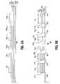
- FIGS. 5A-5Care cross-sectional diagrams along a column of a memory array generally depicting a method of forming a portion of the memory array in accordance with one embodiment of the invention.
- FIG. 5Adepicts a portion of the memory array after several processing steps have occurred. Formation of the type of structure depicted in FIG. 5A is well known and will not be detailed herein.
- FIG. 5Amay depict a semiconductor substrate 505 upon which layers of future gate stacks of non-volatile memory cells and select gates are formed.
- a dielectric layer 533 , a conductive layer 534 , a dielectric layer 535 , and a conductive layer 536have been formed on a substrate 505 .
- an optional cap layer 537such as a layer of silicon nitride, may be formed on conductive layer 536 .
- dielectric layer 533An example of a suitable material for dielectric layer 533 is an oxide that can be blanket deposited or thermally grown on substrate 505 .
- suitable materials for conductive layer 543include polysilicon (polycrystalline silicon) or other doped or undoped silicon materials, such as monocrystalline silicon, nanocrystalline silicon, and amorphous silicon.
- suitable materials for dielectric layer 535include one or more layers of dielectric material, a multi-layer dielectric material commonly referred to as ONO (oxide-nitride-oxide), tantalum oxide, barium strontium titanate, silicon nitride, and other materials providing dielectric properties.
- ONOoxide-nitride-oxide
- tantalum oxidetantalum oxide
- barium strontium titanatesilicon nitride
- conductive layer 536examples include polysilicon, such as conductively-doped polysilicon, a metal or metal-containing layer that may be of aluminum, copper, a refractory metal, or a refractory metal silicide.
- polysiliconsuch as conductively-doped polysilicon
- a metal or metal-containing layerthat may be of aluminum, copper, a refractory metal, or a refractory metal silicide.
- the metals of chromium (Cr), cobalt (Co), hafnium (Hf), molybdenum (Mo), niobium (Nb), tantalum (Ta), titanium (Ti), tungsten (W), vanadium (V) and zirconium (Zr)are generally recognized as refractory metals.
- conductive layer 536may contain multiple metal-containing layers, e.g., a titanium nitride (TiN) barrier layer, a titanium (Ti) adhesion layer overlying the barrier layer, and a tungsten (W) layer overlying the adhesion layer.
- TiNtitanium nitride
- Tititanium adhesion layer
- Wtungsten
- a mask layeris formed and patterned into mask-layer segments 538 1 to 538 N+4 overlying cap layer 537 .
- a photolithographic resist materialcould be deposited as the mask layer overlying cap layer 537 , exposed to a radiation source, such as UV light, and developed to define areas overlying cap layer 537 for removal.
- the mask-layer segments 538are not all of the same length in the column direction (the horizontal direction of FIG. 5A ). Since the lengths of the respective mask-layer segments 538 correspond to the lengths of the gate stacks corresponding to regions underlying the respective mask-layer segments 538 , the gate stacks will not all have the same length.
- mask layer segment 538 1has a length for defining a length of an underlying gate stack corresponding to a drain select gate
- mask layer segment 538 2has a length that is less than the length of mask layer segment 538 1 , for one embodiment, for defining a length of an underlying gate corresponding to another drain select gate
- mask layer segments 538 3 to 538 N+2have a length for defining lengths of a plurality of gate stacks corresponding to a plurality of memory cells
- mask layer segment 538 N+3has a length for defining a length of a gate stack corresponding to a source select gate
- mask layer segment 538 N+4has a length that is greater than the length of mask layer segment 538 N+3 , for another embodiment, for defining a length of a gate stack corresponding to another source select gate. This is discussed further below.
- cap layer 537 and the underlying layersare removed in FIG. 5B , such as by etching or other removal processes, to expose substrate 505 . More than one removal process may be used where the chosen removal process is ineffective at removing an underlying layer.
- gate stacks for memory cells 508 , gate stacks for source select gates 510 and 511 , and gate stacks for drain select gates 512 and 513are defined, as shown in FIG. 5B .
- source select gates 510 and 511 and drain select gates 512 and 513are depicted to have the same structure as memory cells 508 , for improved conduction and faster operation, it is typical to strap conductive layers 534 and 536 of source select gates 510 and 511 and drain select gates 512 and 513 for this embodiment.
- Source/drain regions 550are formed, such as by conductive doping of exposed portions of the substrate 505 , as shown in FIG. 5B . Note that memory cells 508 form a NAND string 506 .
- dielectric layer 533 , conductive layer 534 , dielectric layer 535 , and conductive layer 536respectively form a tunnel-dielectric layer, a floating-gate layer, an intergate-dielectric layer, and a control-gate layer of the respective memory cells.
- dielectric layer 533 , conductive layer 534 , dielectric layer 535could represent a charge-trapping floating-node arrangement, such as an ONO (oxide-nitride-oxide) structure of an NROM memory cell.
- ONOoxide-nitride-oxide
- dielectric layer 533forms a gate-dielectric layer
- conductive layers 534 and 536either alone or strapped together, form a control-gate layer of the respective select gates.
- drain select gates 512 and 513respectively have lengths L 512 and L 513 in the column direction; source select gates 510 and 511 respectively have lengths L 510 and L 511 in the column direction; and memory cells 508 each have a length L 508 in the column direction.
- the length L 513 of drain select gate 513is greater than the length L 512 of drain select gate 512 and thus drain select gate 513 has a greater channel length than drain select gate 512 .
- the length L 511 of source select gate 511is greater than the length L 510 of source select gate 510 and thus source select gate 511 has a greater channel length than source select gate 510 .
- the length L 513 of drain select gate 513is greater than or equal to the length L 511 of source select gate 511 and thus drain select gate 513 has a channel length that is greater than or equal to than source select gate 511 .
- the length L 513 of drain select gate 513 or the length L 512 of drain select gate 512 or the length L 511 of source select gate 511 or the length L 510 of source select gate 510is greater than or equal to the length L 508 of memory cells 508 .
- the length L 513 of drain select gate 513 or the length L 511 of source select gate 511is greater than or equal to the length L 512 of drain select gate 512 or the length L 510 of source select gate 510
- the length L 512 of drain select gate 512 or the length L 510 of source select gate 510is greater than or equal to the length L 508 of memory cells 508
- the length L 508 of memory cells 508may be greater than the lengths of drain select gates 512 and 513 and source select gates 510 and 511 .
- Increasing the length L 513 of drain select gate 513 relative to the length L 512 of drain select gate 512 and/or increasing the length L 511 of source select gate 511 relative to the length L 510 of source select gate 510acts to reduce gate induced drain leakage (GIDL) that can occur through drain select gate 513 and source select gate 511 due to an inherent boosting of their channel voltages during a program operation when a bit line coupled to drain select gate 513 is biased to inhibit programming of the memory cells of the column, a pass voltage is applied to the control gates of the memory cells of the column not targeted for programming, and a programming voltage is applied to one or more of the memory cells of the column target for programming.
- GIDLgate induced drain leakage
- a voltage, e.g., about 2 volts, applied to the control gate of drain select gate 513is greater than a voltage, e.g., about zero volts, applied to the control gate of source select gate 511 during the programming operation, and therefore, there is greater likelihood for punch-through to occur for drain select gate 513 than for source select gate 511 .
- the length L 513 of drain select gate 513is greater than or equal to the length L 511 of source select gate 511 for some embodiments.
- a voltage differencee.g., about 7 volts
- a voltage differencee.g., about 7 volts
- source select gates 510 and 511due to boosting. It is desirable to have the respective portions of these voltage differences that occur across source select gate 510 and drain select gate 512 to be about the same that occurs across adjacent memory cells 508 during programming, e.g., about 1 volt to about 3 volts, with the respective remaining portions of these voltage differences, e.g., about 4 to 6 volts, occurring across source select gate 511 and drain select gate 513 .
- L 513 /L 512 and L 511 /L 510are about 2.
- a bulk insulation layer (or another dielectric layer) 552is formed overlying the structure of FIG. 5B in FIG. 5C that may be followed by removal of excess portions of insulation layer 552 , e.g., by chemical mechanical planerization (CMP), stopping on cap layer 537 so that an upper surface of insulation layer 552 is substantially flush with an upper surface of cap layer 537 .
- One example for the insulation layer 552would be a doped silicate glass. Examples of doped silicate glasses include BSG (borosilicate glass), PSG (phosphosilicate glass), and BPSG (borophosphosilicate glass). Another example for the insulation layer 552 would be TEOS (tetraethylorthosilicate).
- a mask layer(not shown), e.g., an imaging resist layer, is formed overlying insulation layer 552 and cap layer 537 and is patterned for defining areas of insulation layer 552 for removal.
- the areas of insulation layer 552 defined for removalare removed, e.g., by etching, for forming a contact hole 554 that exposes a source/drain region 550 and a contact hole 556 that exposes a source/drain region 550 , as shown in FIG. 5C .
- a slot or a trenchmay be formed in place of contact hole 556 . The slot exposes source/drain regions for multiple columns.
- a contact 560such as a source-line contact
- a contact 562such as a drain-line contact
- blanket depositing a conductive material overlying remaining portions of insulation layer 552 , cap layer 537 , and exposed source/drain regions 550 so as to overfill contact holes 554 and 556e.g., using chemical vapor deposition (CVD) or physical vapor deposition (PVD) techniques, and subsequent removal of the conductive material, e.g., using CMP, stopping on insulation layer 552 and cap layer 537 forms contacts 560 and 562 .
- CVDchemical vapor deposition
- PVDphysical vapor deposition
- conductive material of contacts 560 and 562include polysilicon, such as conductively-doped polysilicon, a metal or metal-containing layer that may be of aluminum, copper, a refractory metal, or a refractory metal silicide.
- conductive material of contacts 560 and 562may contain multiple metal-containing layers, e.g., a titanium nitride (TiN) barrier layer, a titanium (Ti) adhesion layer overlying the barrier layer, and a tungsten (W) layer overlying the adhesion layer.
- a dielectric layer 564is formed overlying contacts 560 and 562 , cap layer 537 , and insulation layer 552 .
- a contact (or via plug) 566such as a bit-line contact, is formed through dielectric layer 564 in direct contact with contact 562 , e.g., by CVD.
- Dielectric layer 564may be of a dielectric material, such as silicon oxides, TEOS, silicon nitrides, or silicon oxynitrides.
- formation of via plug 566includes patterning a mask layer (not shown) formed overlying dielectric layer 564 , followed by the formation of a hole passing through dielectric layer 564 by removal of a portion of dielectric layer 564 , e.g., by etching, defined for removal by the patterning to expose a portion of contact 562 .
- via plug 566may include one or more refractory metals.
- via plug 566may include a barrier layer, such as TiN, in contact with drain contact 562 , a first metal layer, such as titanium (Ti), on the barrier layer, a second metal layer, such as tungsten (W), on the first metal layer.
- a conductive layer 570that may be a metal layer, such as aluminum, is deposited on dielectric layer 564 in electrical contact with via plug 566 , e.g., using CVD.
- Conductive layer 570is patterned, etched, and processed, e.g., using standard processing, to produce individual bit lines therefrom.
Landscapes
- Engineering & Computer Science (AREA)
- Microelectronics & Electronic Packaging (AREA)
- Non-Volatile Memory (AREA)
- Semiconductor Memories (AREA)
Abstract
Description
Claims (21)
Priority Applications (1)
| Application Number | Priority Date | Filing Date | Title |
|---|---|---|---|
| US12/211,545US7729171B2 (en) | 2006-04-12 | 2008-09-16 | Multiple select gate architecture with select gates of different lengths |
Applications Claiming Priority (2)
| Application Number | Priority Date | Filing Date | Title |
|---|---|---|---|
| US11/402,535US7440321B2 (en) | 2006-04-12 | 2006-04-12 | Multiple select gate architecture with select gates of different lengths |
| US12/211,545US7729171B2 (en) | 2006-04-12 | 2008-09-16 | Multiple select gate architecture with select gates of different lengths |
Related Parent Applications (1)
| Application Number | Title | Priority Date | Filing Date |
|---|---|---|---|
| US11/402,535DivisionUS7440321B2 (en) | 2006-04-12 | 2006-04-12 | Multiple select gate architecture with select gates of different lengths |
Publications (2)
| Publication Number | Publication Date |
|---|---|
| US20090011560A1 US20090011560A1 (en) | 2009-01-08 |
| US7729171B2true US7729171B2 (en) | 2010-06-01 |
Family
ID=38604691
Family Applications (2)
| Application Number | Title | Priority Date | Filing Date |
|---|---|---|---|
| US11/402,535Active2027-02-06US7440321B2 (en) | 2006-04-12 | 2006-04-12 | Multiple select gate architecture with select gates of different lengths |
| US12/211,545ActiveUS7729171B2 (en) | 2006-04-12 | 2008-09-16 | Multiple select gate architecture with select gates of different lengths |
Family Applications Before (1)
| Application Number | Title | Priority Date | Filing Date |
|---|---|---|---|
| US11/402,535Active2027-02-06US7440321B2 (en) | 2006-04-12 | 2006-04-12 | Multiple select gate architecture with select gates of different lengths |
Country Status (1)
| Country | Link |
|---|---|
| US (2) | US7440321B2 (en) |
Cited By (2)
| Publication number | Priority date | Publication date | Assignee | Title |
|---|---|---|---|---|
| US20090207667A1 (en)* | 2008-02-15 | 2009-08-20 | Seoul National University Industry Foundation | Nand flash memory array with cut-off gate line and methods for operating and fabricating the same |
| US12400686B2 (en) | 2022-07-12 | 2025-08-26 | Micron Technology, Inc. | Microelectronic devices, and related memory devices and electronic systems |
Families Citing this family (20)
| Publication number | Priority date | Publication date | Assignee | Title |
|---|---|---|---|---|
| US7196930B2 (en)* | 2005-04-27 | 2007-03-27 | Micron Technology, Inc. | Flash memory programming to reduce program disturb |
| US7408810B2 (en)* | 2006-02-22 | 2008-08-05 | Micron Technology, Inc. | Minimizing effects of program disturb in a memory device |
| US7561469B2 (en)* | 2006-03-28 | 2009-07-14 | Micron Technology, Inc. | Programming method to reduce word line to word line breakdown for NAND flash |
| US7538383B1 (en)* | 2006-05-03 | 2009-05-26 | Spansion Llc | Two-bit memory cell having conductive charge storage segments and method for fabricating same |
| US7471565B2 (en) | 2006-08-22 | 2008-12-30 | Micron Technology, Inc. | Reducing effects of program disturb in a memory device |
| TW200908301A (en)* | 2007-08-08 | 2009-02-16 | Nanya Technology Corp | Flash memory |
| US7733705B2 (en)* | 2008-03-13 | 2010-06-08 | Micron Technology, Inc. | Reduction of punch-through disturb during programming of a memory device |
| JP5491705B2 (en)* | 2008-05-22 | 2014-05-14 | 株式会社東芝 | Semiconductor device |
| US7939911B2 (en)* | 2008-08-14 | 2011-05-10 | International Business Machines Corporation | Back-end-of-line resistive semiconductor structures |
| US7977201B2 (en)* | 2008-08-14 | 2011-07-12 | International Business Machines Corporation | Methods for forming back-end-of-line resistive semiconductor structures |
| US8542534B2 (en)* | 2010-04-08 | 2013-09-24 | Micron Technology, Inc. | Select gate programming in a memory device |
| US8797806B2 (en) | 2011-08-15 | 2014-08-05 | Micron Technology, Inc. | Apparatus and methods including source gates |
| KR20130088348A (en)* | 2012-01-31 | 2013-08-08 | 에스케이하이닉스 주식회사 | 3-dimensional non-volatile memory device |
| US10541029B2 (en) | 2012-08-01 | 2020-01-21 | Micron Technology, Inc. | Partial block memory operations |
| US9318199B2 (en) | 2012-10-26 | 2016-04-19 | Micron Technology, Inc. | Partial page memory operations |
| US9318200B2 (en) | 2014-08-11 | 2016-04-19 | Micron Technology, Inc. | Methods and apparatuses including a string of memory cells having a first select transistor coupled to a second select transistor |
| KR20160062498A (en)* | 2014-11-25 | 2016-06-02 | 에스케이하이닉스 주식회사 | Semiconductor memory device and operating method thereof |
| US9715938B2 (en) | 2015-09-21 | 2017-07-25 | Sandisk Technologies Llc | Non-volatile memory with supplemental select gates |
| US9953717B2 (en) | 2016-03-31 | 2018-04-24 | Sandisk Technologies Llc | NAND structure with tier select gate transistors |
| US9728266B1 (en)* | 2016-07-08 | 2017-08-08 | Micron Technology, Inc. | Memory device including multiple select gates and different bias conditions |
Citations (70)
| Publication number | Priority date | Publication date | Assignee | Title |
|---|---|---|---|---|
| US5257225A (en) | 1992-03-12 | 1993-10-26 | Micron Technology, Inc. | Method for programming programmable devices by utilizing single or multiple pulses varying in pulse width and amplitude |
| US5357463A (en) | 1992-11-17 | 1994-10-18 | Micron Semiconductor, Inc. | Method for reverse programming of a flash EEPROM |
| US5424993A (en) | 1993-11-15 | 1995-06-13 | Micron Technology, Inc. | Programming method for the selective healing of over-erased cells on a flash erasable programmable read-only memory device |
| US5511022A (en) | 1988-12-15 | 1996-04-23 | Samsung Electronics Co., Ltd. | Depletion mode NAND string electrically erasable programmable semiconductor memory device and method for erasing and programming thereof |
| US5528547A (en) | 1990-04-12 | 1996-06-18 | Kabushiki Kaisha Toshiba | Electrically erasable programmable read-only memory with electric field decreasing controller |
| US5621684A (en) | 1995-03-31 | 1997-04-15 | Samsung Electronics Co., Ltd. | Nonvolatile semiconductor member with different pass potential applied to the first two adjacent word |
| US5677873A (en) | 1995-09-19 | 1997-10-14 | Samsung Electronics Co., Ltd. | Methods of programming flash EEPROM integrated circuit memory devices to prevent inadvertent programming of nondesignated NAND memory cells therein |
| US5677875A (en) | 1995-02-28 | 1997-10-14 | Nec Corporation | Non-volatile semiconductor memory device configured to minimize variations in threshold voltages of non-written memory cells and potentials of selected bit lines |
| US5680350A (en) | 1994-12-14 | 1997-10-21 | Micron Technology, Inc. | Method for narrowing threshold voltage distribution in a block erased flash memory array |
| US5715194A (en) | 1996-07-24 | 1998-02-03 | Advanced Micro Devices, Inc. | Bias scheme of program inhibit for random programming in a nand flash memory |
| US5768287A (en) | 1996-10-24 | 1998-06-16 | Micron Quantum Devices, Inc. | Apparatus and method for programming multistate memory device |
| US5771346A (en) | 1996-10-24 | 1998-06-23 | Micron Quantum Devices, Inc. | Apparatus and method for detecting over-programming condition in multistate memory device |
| US5907855A (en) | 1996-10-15 | 1999-05-25 | Micron Technology, Inc. | Apparatus and method for reducing programming cycles for multistate memory system |
| US5917757A (en) | 1996-08-01 | 1999-06-29 | Aplus Flash Technology, Inc. | Flash memory with high speed erasing structure using thin oxide semiconductor devices |
| US5920501A (en) | 1997-12-12 | 1999-07-06 | Micron Technology, Inc. | Flash memory system and method for monitoring the disturb effect on memory cell blocks due to high voltage conditions of other memory cell blocks |
| US5930168A (en) | 1998-03-20 | 1999-07-27 | Micron Technology, Inc. | Flash memory with adjustable write operation timing |
| US5959892A (en) | 1997-08-26 | 1999-09-28 | Macronix International Co., Ltd. | Apparatus and method for programming virtual ground EPROM array cell without disturbing adjacent cells |
| US5991202A (en) | 1998-09-24 | 1999-11-23 | Advanced Micro Devices, Inc. | Method for reducing program disturb during self-boosting in a NAND flash memory |
| US6061270A (en) | 1997-12-31 | 2000-05-09 | Samsung Electronics Co., Ltd. | Method for programming a non-volatile memory device with program disturb control |
| US6107658A (en) | 1997-02-27 | 2000-08-22 | Kabushiki Kaisha Toshiba | Non-volatile semiconductor memory device |
| US6157575A (en)* | 1998-03-26 | 2000-12-05 | Samsung Electronics Co., Ltd | Nonvolatile memory device and operating method thereof |
| US6163048A (en) | 1995-10-25 | 2000-12-19 | Cypress Semiconductor Corporation | Semiconductor non-volatile memory device having a NAND cell structure |
| US6240023B1 (en) | 1998-02-27 | 2001-05-29 | Micron Technology, Inc. | Method for efficiently executing soft programming of a memory block |
| US6240016B1 (en) | 1999-12-17 | 2001-05-29 | Advanced Micro Devices, Inc. | Method to reduce read gate disturb for flash EEPROM application |
| US6370062B2 (en) | 1999-12-10 | 2002-04-09 | Samsung Electronics Co., Ltd. | NAND-type flash memory device and method of operating the same |
| US6380033B1 (en) | 1999-09-20 | 2002-04-30 | Advanced Micro Devices, Inc. | Process to improve read disturb for NAND flash memory devices |
| US20020060926A1 (en) | 2000-11-22 | 2002-05-23 | Samsung Electronics Co., Ltd. | Flash memory device capable of preventing program disturb and method for programming the same |
| US20020075727A1 (en) | 2000-12-14 | 2002-06-20 | Samsung Electronics Co., Ltd. | Non-volatile semiconductor memory device capable of preventing program disturb due to noise voltage induced at a string select line and program method thereof |
| US20020149958A1 (en) | 2001-04-11 | 2002-10-17 | Mitsubishi Denki Kabushiki Kaisha | Non-volatile semiconductor memory |
| US6487117B1 (en) | 1999-02-01 | 2002-11-26 | Samsung Electronics Co., Ltd. | Method for programming NAND-type flash memory device using bulk bias |
| US6493270B2 (en) | 1999-07-01 | 2002-12-10 | Micron Technology, Inc. | Leakage detection in programming algorithm for a flash memory device |
| US6498752B1 (en) | 2001-08-27 | 2002-12-24 | Aplus Flash Technology, Inc. | Three step write process used for a nonvolatile NOR type EEPROM memory |
| US6519181B2 (en) | 2000-12-29 | 2003-02-11 | Hynix Semiconductor Inc. | Flash memory device |
| US6522584B1 (en) | 2001-08-02 | 2003-02-18 | Micron Technology, Inc. | Programming methods for multi-level flash EEPROMs |
| US6620682B1 (en) | 2001-02-27 | 2003-09-16 | Aplus Flash Technology, Inc. | Set of three level concurrent word line bias conditions for a nor type flash memory array |
| US6657915B2 (en) | 2000-12-06 | 2003-12-02 | Samsung Electronics Co., Ltd. | Wordline driver for ensuring equal stress to wordlines in multi row address disturb test and method of driving the wordline driver |
| US6660585B1 (en) | 2000-03-21 | 2003-12-09 | Aplus Flash Technology, Inc. | Stacked gate flash memory cell with reduced disturb conditions |
| US6661707B2 (en) | 2001-02-16 | 2003-12-09 | Samsung Electronics Co., Ltd. | Method of programming NAND-type flash memory |
| US6707714B2 (en) | 2002-01-22 | 2004-03-16 | Fujitsu Limited | Read disturb alleviated flash memory |
| US20040080980A1 (en) | 2002-10-23 | 2004-04-29 | Chang-Hyun Lee | Methods of programming non-volatile semiconductor memory devices including coupling voltages and related devices |
| US20040152262A1 (en)* | 2003-02-05 | 2004-08-05 | Kabushiki Kaisha Toshiba | Nonvolatile semiconductor memory, fabrication method for the same, semiconductor integrated circuits and systems |
| US6798694B2 (en) | 2002-08-29 | 2004-09-28 | Micron Technology, Inc. | Method for reducing drain disturb in programming |
| US20040237000A1 (en) | 2003-05-08 | 2004-11-25 | Micron Technology, Inc. | Program failure recovery |
| US20050088890A1 (en) | 2002-11-29 | 2005-04-28 | Yasuhiko Matsunaga | NAND type flash EEPROM in which sequential programming process is performed by using different intermediate voltages |
| US6925011B2 (en) | 2002-12-26 | 2005-08-02 | Micron Technology, Inc. | Programming flash memories |
| US20050226055A1 (en) | 2004-04-13 | 2005-10-13 | Guterman Daniel C | Programming inhibit for non-volatile memory |
| US20050265097A1 (en) | 1997-05-14 | 2005-12-01 | Kabushiki Kaisha Toshiba | Nonvolatile semiconductor memory device |
| US6975542B2 (en) | 2003-05-08 | 2005-12-13 | Micron Technology, Inc. | NAND flash memory with improved read and verification threshold uniformity |
| US6977842B2 (en) | 2003-09-16 | 2005-12-20 | Micron Technology, Inc. | Boosted substrate/tub programming for flash memories |
| US6982905B2 (en) | 2003-10-09 | 2006-01-03 | Micron Technology, Inc. | Method and apparatus for reading NAND flash memory array |
| US20060002167A1 (en) | 2004-06-30 | 2006-01-05 | Micron Technology, Inc. | Minimizing adjacent wordline disturb in a memory device |
| US20060023502A1 (en) | 2002-09-24 | 2006-02-02 | Raul-Adrian Cernea | Non-volatile memory and method with reduced neighboring field errors |
| US7020017B2 (en) | 2004-04-06 | 2006-03-28 | Sandisk Corporation | Variable programming of non-volatile memory |
| US7099193B2 (en) | 2003-09-08 | 2006-08-29 | Kabushiki Kaisha Toshiba | Nonvolatile semiconductor memory device, electronic card and electronic apparatus |
| US7120059B2 (en) | 2004-07-06 | 2006-10-10 | Macronix International Co., Ltd. | Memory array including multiple-gate charge trapping non-volatile cells |
| US20060274583A1 (en) | 2005-06-03 | 2006-12-07 | Jeffrey Lutze | Starting program voltage shift with cycling of non-volatile memory |
| US7161833B2 (en) | 2004-02-06 | 2007-01-09 | Sandisk Corporation | Self-boosting system for flash memory cells |
| US20070047314A1 (en) | 2005-08-31 | 2007-03-01 | Micron Technology, Inc. | Programming method for NAND EEPROM |
| US7245534B2 (en) | 2004-05-31 | 2007-07-17 | Kabushiki Kaisha Toshiba | Nonvolatile semiconductor memory |
| US20070177429A1 (en) | 2006-01-24 | 2007-08-02 | Kabushiki Kaisha Toshiba | Nonvolatile semiconductor memory and nonvolatile memory system using thereof |
| US20070236992A1 (en) | 2006-03-30 | 2007-10-11 | Ken Oowada | Self-boosting method with suppression of high lateral electric fields |
| US20070258286A1 (en) | 2006-05-05 | 2007-11-08 | Masaaki Higashitani | Boosting methods for nand flash memory |
| US7355889B2 (en) | 2005-12-19 | 2008-04-08 | Sandisk Corporation | Method for programming non-volatile memory with reduced program disturb using modified pass voltages |
| US20080101126A1 (en) | 2006-10-30 | 2008-05-01 | Gerrit Jan Hemink | Faster programming of highest multi-level state for non-volatile memory |
| US7394693B2 (en) | 2005-08-31 | 2008-07-01 | Micron Technology, Inc. | Multiple select gate architecture |
| US7408810B2 (en) | 2006-02-22 | 2008-08-05 | Micron Technology, Inc. | Minimizing effects of program disturb in a memory device |
| US20080316827A1 (en)* | 2007-06-25 | 2008-12-25 | Masaaki Higashitani | Non-volatile storage with individually controllable shield plates between storage elements |
| US7471565B2 (en) | 2006-08-22 | 2008-12-30 | Micron Technology, Inc. | Reducing effects of program disturb in a memory device |
| US7561469B2 (en) | 2006-03-28 | 2009-07-14 | Micron Technology, Inc. | Programming method to reduce word line to word line breakdown for NAND flash |
| US20090189211A1 (en)* | 2008-01-25 | 2009-07-30 | Takashi Orimoto | Non-Volatile Memory Arrays Having Dual Control Gate Cell Structures And A Thick Control Gate Dielectric And Methods Of Forming |
Family Cites Families (2)
| Publication number | Priority date | Publication date | Assignee | Title |
|---|---|---|---|---|
| US739463A (en)* | 1902-02-03 | 1903-09-22 | Weber Railway Joint Mfg Company | Railroad-rail joint. |
| US5550474A (en)* | 1985-05-03 | 1996-08-27 | Dahl; Ernest A. | Battery electrolyte-level and electrolyte-stratification sensing system |
- 2006
- 2006-04-12USUS11/402,535patent/US7440321B2/enactiveActive
- 2008
- 2008-09-16USUS12/211,545patent/US7729171B2/enactiveActive
Patent Citations (75)
| Publication number | Priority date | Publication date | Assignee | Title |
|---|---|---|---|---|
| US5511022A (en) | 1988-12-15 | 1996-04-23 | Samsung Electronics Co., Ltd. | Depletion mode NAND string electrically erasable programmable semiconductor memory device and method for erasing and programming thereof |
| US5528547A (en) | 1990-04-12 | 1996-06-18 | Kabushiki Kaisha Toshiba | Electrically erasable programmable read-only memory with electric field decreasing controller |
| US5257225A (en) | 1992-03-12 | 1993-10-26 | Micron Technology, Inc. | Method for programming programmable devices by utilizing single or multiple pulses varying in pulse width and amplitude |
| US5357463A (en) | 1992-11-17 | 1994-10-18 | Micron Semiconductor, Inc. | Method for reverse programming of a flash EEPROM |
| US5424993A (en) | 1993-11-15 | 1995-06-13 | Micron Technology, Inc. | Programming method for the selective healing of over-erased cells on a flash erasable programmable read-only memory device |
| US5680350A (en) | 1994-12-14 | 1997-10-21 | Micron Technology, Inc. | Method for narrowing threshold voltage distribution in a block erased flash memory array |
| US5677875A (en) | 1995-02-28 | 1997-10-14 | Nec Corporation | Non-volatile semiconductor memory device configured to minimize variations in threshold voltages of non-written memory cells and potentials of selected bit lines |
| US5621684A (en) | 1995-03-31 | 1997-04-15 | Samsung Electronics Co., Ltd. | Nonvolatile semiconductor member with different pass potential applied to the first two adjacent word |
| US5677873A (en) | 1995-09-19 | 1997-10-14 | Samsung Electronics Co., Ltd. | Methods of programming flash EEPROM integrated circuit memory devices to prevent inadvertent programming of nondesignated NAND memory cells therein |
| US6163048A (en) | 1995-10-25 | 2000-12-19 | Cypress Semiconductor Corporation | Semiconductor non-volatile memory device having a NAND cell structure |
| US5715194A (en) | 1996-07-24 | 1998-02-03 | Advanced Micro Devices, Inc. | Bias scheme of program inhibit for random programming in a nand flash memory |
| US5917757A (en) | 1996-08-01 | 1999-06-29 | Aplus Flash Technology, Inc. | Flash memory with high speed erasing structure using thin oxide semiconductor devices |
| US5907855A (en) | 1996-10-15 | 1999-05-25 | Micron Technology, Inc. | Apparatus and method for reducing programming cycles for multistate memory system |
| US5768287A (en) | 1996-10-24 | 1998-06-16 | Micron Quantum Devices, Inc. | Apparatus and method for programming multistate memory device |
| US5771346A (en) | 1996-10-24 | 1998-06-23 | Micron Quantum Devices, Inc. | Apparatus and method for detecting over-programming condition in multistate memory device |
| US6107658A (en) | 1997-02-27 | 2000-08-22 | Kabushiki Kaisha Toshiba | Non-volatile semiconductor memory device |
| US20050265097A1 (en) | 1997-05-14 | 2005-12-01 | Kabushiki Kaisha Toshiba | Nonvolatile semiconductor memory device |
| US5959892A (en) | 1997-08-26 | 1999-09-28 | Macronix International Co., Ltd. | Apparatus and method for programming virtual ground EPROM array cell without disturbing adjacent cells |
| US5920501A (en) | 1997-12-12 | 1999-07-06 | Micron Technology, Inc. | Flash memory system and method for monitoring the disturb effect on memory cell blocks due to high voltage conditions of other memory cell blocks |
| US6061270A (en) | 1997-12-31 | 2000-05-09 | Samsung Electronics Co., Ltd. | Method for programming a non-volatile memory device with program disturb control |
| US6240023B1 (en) | 1998-02-27 | 2001-05-29 | Micron Technology, Inc. | Method for efficiently executing soft programming of a memory block |
| US5930168A (en) | 1998-03-20 | 1999-07-27 | Micron Technology, Inc. | Flash memory with adjustable write operation timing |
| US6157575A (en)* | 1998-03-26 | 2000-12-05 | Samsung Electronics Co., Ltd | Nonvolatile memory device and operating method thereof |
| US5991202A (en) | 1998-09-24 | 1999-11-23 | Advanced Micro Devices, Inc. | Method for reducing program disturb during self-boosting in a NAND flash memory |
| US6487117B1 (en) | 1999-02-01 | 2002-11-26 | Samsung Electronics Co., Ltd. | Method for programming NAND-type flash memory device using bulk bias |
| US6493270B2 (en) | 1999-07-01 | 2002-12-10 | Micron Technology, Inc. | Leakage detection in programming algorithm for a flash memory device |
| US6380033B1 (en) | 1999-09-20 | 2002-04-30 | Advanced Micro Devices, Inc. | Process to improve read disturb for NAND flash memory devices |
| US6370062B2 (en) | 1999-12-10 | 2002-04-09 | Samsung Electronics Co., Ltd. | NAND-type flash memory device and method of operating the same |
| US6240016B1 (en) | 1999-12-17 | 2001-05-29 | Advanced Micro Devices, Inc. | Method to reduce read gate disturb for flash EEPROM application |
| US6660585B1 (en) | 2000-03-21 | 2003-12-09 | Aplus Flash Technology, Inc. | Stacked gate flash memory cell with reduced disturb conditions |
| US20020060926A1 (en) | 2000-11-22 | 2002-05-23 | Samsung Electronics Co., Ltd. | Flash memory device capable of preventing program disturb and method for programming the same |
| US6469933B2 (en) | 2000-11-22 | 2002-10-22 | Samsung Electronics Co., Ltd. | Flash memory device capable of preventing program disturb and method for programming the same |
| US6657915B2 (en) | 2000-12-06 | 2003-12-02 | Samsung Electronics Co., Ltd. | Wordline driver for ensuring equal stress to wordlines in multi row address disturb test and method of driving the wordline driver |
| US20020075727A1 (en) | 2000-12-14 | 2002-06-20 | Samsung Electronics Co., Ltd. | Non-volatile semiconductor memory device capable of preventing program disturb due to noise voltage induced at a string select line and program method thereof |
| US6519181B2 (en) | 2000-12-29 | 2003-02-11 | Hynix Semiconductor Inc. | Flash memory device |
| US6661707B2 (en) | 2001-02-16 | 2003-12-09 | Samsung Electronics Co., Ltd. | Method of programming NAND-type flash memory |
| US6620682B1 (en) | 2001-02-27 | 2003-09-16 | Aplus Flash Technology, Inc. | Set of three level concurrent word line bias conditions for a nor type flash memory array |
| US20020149958A1 (en) | 2001-04-11 | 2002-10-17 | Mitsubishi Denki Kabushiki Kaisha | Non-volatile semiconductor memory |
| US6522584B1 (en) | 2001-08-02 | 2003-02-18 | Micron Technology, Inc. | Programming methods for multi-level flash EEPROMs |
| US6498752B1 (en) | 2001-08-27 | 2002-12-24 | Aplus Flash Technology, Inc. | Three step write process used for a nonvolatile NOR type EEPROM memory |
| US6707714B2 (en) | 2002-01-22 | 2004-03-16 | Fujitsu Limited | Read disturb alleviated flash memory |
| US6798694B2 (en) | 2002-08-29 | 2004-09-28 | Micron Technology, Inc. | Method for reducing drain disturb in programming |
| US20060023502A1 (en) | 2002-09-24 | 2006-02-02 | Raul-Adrian Cernea | Non-volatile memory and method with reduced neighboring field errors |
| US20040080980A1 (en) | 2002-10-23 | 2004-04-29 | Chang-Hyun Lee | Methods of programming non-volatile semiconductor memory devices including coupling voltages and related devices |
| US20050088890A1 (en) | 2002-11-29 | 2005-04-28 | Yasuhiko Matsunaga | NAND type flash EEPROM in which sequential programming process is performed by using different intermediate voltages |
| US6925011B2 (en) | 2002-12-26 | 2005-08-02 | Micron Technology, Inc. | Programming flash memories |
| US20040152262A1 (en)* | 2003-02-05 | 2004-08-05 | Kabushiki Kaisha Toshiba | Nonvolatile semiconductor memory, fabrication method for the same, semiconductor integrated circuits and systems |
| US20040237000A1 (en) | 2003-05-08 | 2004-11-25 | Micron Technology, Inc. | Program failure recovery |
| US6975542B2 (en) | 2003-05-08 | 2005-12-13 | Micron Technology, Inc. | NAND flash memory with improved read and verification threshold uniformity |
| US7099193B2 (en) | 2003-09-08 | 2006-08-29 | Kabushiki Kaisha Toshiba | Nonvolatile semiconductor memory device, electronic card and electronic apparatus |
| US6977842B2 (en) | 2003-09-16 | 2005-12-20 | Micron Technology, Inc. | Boosted substrate/tub programming for flash memories |
| US6982905B2 (en) | 2003-10-09 | 2006-01-03 | Micron Technology, Inc. | Method and apparatus for reading NAND flash memory array |
| US7161833B2 (en) | 2004-02-06 | 2007-01-09 | Sandisk Corporation | Self-boosting system for flash memory cells |
| US7020017B2 (en) | 2004-04-06 | 2006-03-28 | Sandisk Corporation | Variable programming of non-volatile memory |
| US20050226055A1 (en) | 2004-04-13 | 2005-10-13 | Guterman Daniel C | Programming inhibit for non-volatile memory |
| US7245534B2 (en) | 2004-05-31 | 2007-07-17 | Kabushiki Kaisha Toshiba | Nonvolatile semiconductor memory |
| US20060002167A1 (en) | 2004-06-30 | 2006-01-05 | Micron Technology, Inc. | Minimizing adjacent wordline disturb in a memory device |
| US7212435B2 (en) | 2004-06-30 | 2007-05-01 | Micron Technology, Inc. | Minimizing adjacent wordline disturb in a memory device |
| US7120059B2 (en) | 2004-07-06 | 2006-10-10 | Macronix International Co., Ltd. | Memory array including multiple-gate charge trapping non-volatile cells |
| US20060274583A1 (en) | 2005-06-03 | 2006-12-07 | Jeffrey Lutze | Starting program voltage shift with cycling of non-volatile memory |
| US20080253187A1 (en) | 2005-08-31 | 2008-10-16 | Micron Technology, Inc. | Multiple select gate architecture |
| US7499330B2 (en) | 2005-08-31 | 2009-03-03 | Micron Technology, Inc. | Programming method for NAND EEPROM |
| US7292476B2 (en) | 2005-08-31 | 2007-11-06 | Micron Technology, Inc. | Programming method for NAND EEPROM |
| US7394693B2 (en) | 2005-08-31 | 2008-07-01 | Micron Technology, Inc. | Multiple select gate architecture |
| US20070047314A1 (en) | 2005-08-31 | 2007-03-01 | Micron Technology, Inc. | Programming method for NAND EEPROM |
| US7355889B2 (en) | 2005-12-19 | 2008-04-08 | Sandisk Corporation | Method for programming non-volatile memory with reduced program disturb using modified pass voltages |
| US20070177429A1 (en) | 2006-01-24 | 2007-08-02 | Kabushiki Kaisha Toshiba | Nonvolatile semiconductor memory and nonvolatile memory system using thereof |
| US7408810B2 (en) | 2006-02-22 | 2008-08-05 | Micron Technology, Inc. | Minimizing effects of program disturb in a memory device |
| US7561469B2 (en) | 2006-03-28 | 2009-07-14 | Micron Technology, Inc. | Programming method to reduce word line to word line breakdown for NAND flash |
| US20070236992A1 (en) | 2006-03-30 | 2007-10-11 | Ken Oowada | Self-boosting method with suppression of high lateral electric fields |
| US20070258286A1 (en) | 2006-05-05 | 2007-11-08 | Masaaki Higashitani | Boosting methods for nand flash memory |
| US7471565B2 (en) | 2006-08-22 | 2008-12-30 | Micron Technology, Inc. | Reducing effects of program disturb in a memory device |
| US20080101126A1 (en) | 2006-10-30 | 2008-05-01 | Gerrit Jan Hemink | Faster programming of highest multi-level state for non-volatile memory |
| US20080316827A1 (en)* | 2007-06-25 | 2008-12-25 | Masaaki Higashitani | Non-volatile storage with individually controllable shield plates between storage elements |
| US20090189211A1 (en)* | 2008-01-25 | 2009-07-30 | Takashi Orimoto | Non-Volatile Memory Arrays Having Dual Control Gate Cell Structures And A Thick Control Gate Dielectric And Methods Of Forming |
Non-Patent Citations (4)
| Title |
|---|
| K. Suh et al., "A 3.3 V 32 Mb NAND Flash Memory with Incremental Step Pulse Programming Scheme" IEEE Journal of Solid-State Circuits, IEEE Inc., New York, NY, vol. 30, No. 11, Nov. 1995, pp. 1149-1156. |
| S. Satoh et al., A Novel Gate-Offset NAND Cell (GOC-NAND) Technology Suitable for High-Density and Low-Voltage-Operation Flash Memories, Microelectronics Engineering Laboratory, Japan, IEEE, 1999, 4 pgs. |
| S. Satoh et al., A Novel Isolation-Scaling Technology for NAND EEPROMs with the Minimized Program Disturbance, Microelectronics Engineering Laboratory, Japan, IEEE, 1997, IEDM 97-291, pp. 11.6.1-11.6.4. |
| T. Jung et al., "A 117-mm2 3.3-V Only 128-Mb Multilevel NAND Flash Memory for Mass Storage Applications" IEEE Journal of Solid-State Circuits, IEEE Inc., New York, NY, U.S., vol. 31, No. 11, Nov. 1996, pp. 1575-1583. |
Cited By (4)
| Publication number | Priority date | Publication date | Assignee | Title |
|---|---|---|---|---|
| US20090207667A1 (en)* | 2008-02-15 | 2009-08-20 | Seoul National University Industry Foundation | Nand flash memory array with cut-off gate line and methods for operating and fabricating the same |
| US7995390B2 (en)* | 2008-02-15 | 2011-08-09 | Seoul National University Industry Foundation | NAND flash memory array with cut-off gate line and methods for operating and fabricating the same |
| US8394698B2 (en) | 2008-02-15 | 2013-03-12 | Seoul National University Industry Foundation | NAND flash memory array with cut-off gate line and methods for operating and fabricating the same |
| US12400686B2 (en) | 2022-07-12 | 2025-08-26 | Micron Technology, Inc. | Microelectronic devices, and related memory devices and electronic systems |
Also Published As
| Publication number | Publication date |
|---|---|
| US20090011560A1 (en) | 2009-01-08 |
| US7440321B2 (en) | 2008-10-21 |
| US20070242515A1 (en) | 2007-10-18 |
Similar Documents
| Publication | Publication Date | Title |
|---|---|---|
| US7729171B2 (en) | Multiple select gate architecture with select gates of different lengths | |
| US7995391B2 (en) | Multiple select gates with non-volatile memory cells | |
| US7697335B2 (en) | Multiple select gate architecture | |
| US7811935B2 (en) | Isolation regions and their formation | |
| US7452766B2 (en) | Finned memory cells and the fabrication thereof | |
| US7282762B2 (en) | 4F2 EEPROM NROM memory arrays with vertical devices | |
| US8446767B2 (en) | Memories and their formation | |
| US8284616B2 (en) | Trench memory structure operation | |
| US20070195571A1 (en) | Bit line coupling | |
| US20060267070A1 (en) | Gate coupling in floating-gate memory cells | |
| US7898856B2 (en) | Memory cell heights | |
| US8693231B2 (en) | Couplings within memory devices | |
| US8519469B2 (en) | Select gates for memory | |
| US20060046402A1 (en) | Flash cell structures and methods of formation |
Legal Events
| Date | Code | Title | Description |
|---|---|---|---|
| FEPP | Fee payment procedure | Free format text:PAYOR NUMBER ASSIGNED (ORIGINAL EVENT CODE: ASPN); ENTITY STATUS OF PATENT OWNER: LARGE ENTITY | |
| STCF | Information on status: patent grant | Free format text:PATENTED CASE | |
| FPAY | Fee payment | Year of fee payment:4 | |
| AS | Assignment | Owner name:U.S. BANK NATIONAL ASSOCIATION, AS COLLATERAL AGENT, CALIFORNIA Free format text:SECURITY INTEREST;ASSIGNOR:MICRON TECHNOLOGY, INC.;REEL/FRAME:038669/0001 Effective date:20160426 Owner name:U.S. BANK NATIONAL ASSOCIATION, AS COLLATERAL AGEN Free format text:SECURITY INTEREST;ASSIGNOR:MICRON TECHNOLOGY, INC.;REEL/FRAME:038669/0001 Effective date:20160426 | |
| AS | Assignment | Owner name:MORGAN STANLEY SENIOR FUNDING, INC., AS COLLATERAL AGENT, MARYLAND Free format text:PATENT SECURITY AGREEMENT;ASSIGNOR:MICRON TECHNOLOGY, INC.;REEL/FRAME:038954/0001 Effective date:20160426 Owner name:MORGAN STANLEY SENIOR FUNDING, INC., AS COLLATERAL Free format text:PATENT SECURITY AGREEMENT;ASSIGNOR:MICRON TECHNOLOGY, INC.;REEL/FRAME:038954/0001 Effective date:20160426 | |
| AS | Assignment | Owner name:U.S. BANK NATIONAL ASSOCIATION, AS COLLATERAL AGENT, CALIFORNIA Free format text:CORRECTIVE ASSIGNMENT TO CORRECT THE REPLACE ERRONEOUSLY FILED PATENT #7358718 WITH THE CORRECT PATENT #7358178 PREVIOUSLY RECORDED ON REEL 038669 FRAME 0001. ASSIGNOR(S) HEREBY CONFIRMS THE SECURITY INTEREST;ASSIGNOR:MICRON TECHNOLOGY, INC.;REEL/FRAME:043079/0001 Effective date:20160426 Owner name:U.S. BANK NATIONAL ASSOCIATION, AS COLLATERAL AGEN Free format text:CORRECTIVE ASSIGNMENT TO CORRECT THE REPLACE ERRONEOUSLY FILED PATENT #7358718 WITH THE CORRECT PATENT #7358178 PREVIOUSLY RECORDED ON REEL 038669 FRAME 0001. ASSIGNOR(S) HEREBY CONFIRMS THE SECURITY INTEREST;ASSIGNOR:MICRON TECHNOLOGY, INC.;REEL/FRAME:043079/0001 Effective date:20160426 | |
| MAFP | Maintenance fee payment | Free format text:PAYMENT OF MAINTENANCE FEE, 8TH YEAR, LARGE ENTITY (ORIGINAL EVENT CODE: M1552) Year of fee payment:8 | |
| AS | Assignment | Owner name:JPMORGAN CHASE BANK, N.A., AS COLLATERAL AGENT, ILLINOIS Free format text:SECURITY INTEREST;ASSIGNORS:MICRON TECHNOLOGY, INC.;MICRON SEMICONDUCTOR PRODUCTS, INC.;REEL/FRAME:047540/0001 Effective date:20180703 Owner name:JPMORGAN CHASE BANK, N.A., AS COLLATERAL AGENT, IL Free format text:SECURITY INTEREST;ASSIGNORS:MICRON TECHNOLOGY, INC.;MICRON SEMICONDUCTOR PRODUCTS, INC.;REEL/FRAME:047540/0001 Effective date:20180703 | |
| AS | Assignment | Owner name:MICRON TECHNOLOGY, INC., IDAHO Free format text:RELEASE BY SECURED PARTY;ASSIGNOR:U.S. BANK NATIONAL ASSOCIATION, AS COLLATERAL AGENT;REEL/FRAME:047243/0001 Effective date:20180629 | |
| AS | Assignment | Owner name:MICRON TECHNOLOGY, INC., IDAHO Free format text:RELEASE BY SECURED PARTY;ASSIGNOR:MORGAN STANLEY SENIOR FUNDING, INC., AS COLLATERAL AGENT;REEL/FRAME:050937/0001 Effective date:20190731 | |
| AS | Assignment | Owner name:MICRON SEMICONDUCTOR PRODUCTS, INC., IDAHO Free format text:RELEASE BY SECURED PARTY;ASSIGNOR:JPMORGAN CHASE BANK, N.A., AS COLLATERAL AGENT;REEL/FRAME:051028/0001 Effective date:20190731 Owner name:MICRON TECHNOLOGY, INC., IDAHO Free format text:RELEASE BY SECURED PARTY;ASSIGNOR:JPMORGAN CHASE BANK, N.A., AS COLLATERAL AGENT;REEL/FRAME:051028/0001 Effective date:20190731 | |
| MAFP | Maintenance fee payment | Free format text:PAYMENT OF MAINTENANCE FEE, 12TH YEAR, LARGE ENTITY (ORIGINAL EVENT CODE: M1553); ENTITY STATUS OF PATENT OWNER: LARGE ENTITY Year of fee payment:12 |