US7728397B2 - Coupled nano-resonating energy emitting structures - Google Patents
Coupled nano-resonating energy emitting structuresDownload PDFInfo
- Publication number
- US7728397B2 US7728397B2US11/418,123US41812306AUS7728397B2US 7728397 B2US7728397 B2US 7728397B2US 41812306 AUS41812306 AUS 41812306AUS 7728397 B2US7728397 B2US 7728397B2
- Authority
- US
- United States
- Prior art keywords
- nano
- ultra
- charged particles
- substrate
- small
- Prior art date
- Legal status (The legal status is an assumption and is not a legal conclusion. Google has not performed a legal analysis and makes no representation as to the accuracy of the status listed.)
- Active - Reinstated, expires
Links
- 239000002245particleSubstances0.000claimsabstractdescription34
- 238000003491arrayMethods0.000claimsabstractdescription17
- 239000000758substrateSubstances0.000claimsdescription30
- 230000005670electromagnetic radiationEffects0.000claimsdescription14
- 239000003989dielectric materialSubstances0.000claimsdescription10
- 150000002500ionsChemical class0.000claimsdescription6
- 229910052751metalInorganic materials0.000claimsdescription5
- 239000002184metalSubstances0.000claimsdescription5
- 239000004020conductorSubstances0.000claimsdescription3
- 150000002739metalsChemical class0.000claimsdescription3
- 229910045601alloyInorganic materials0.000claimsdescription2
- 239000000956alloySubstances0.000claimsdescription2
- 239000000463materialSubstances0.000description9
- 239000011810insulating materialSubstances0.000description8
- 238000000034methodMethods0.000description7
- 230000005284excitationEffects0.000description3
- 230000005855radiationEffects0.000description3
- 238000010894electron beam technologyMethods0.000description2
- -1for exampleSubstances0.000description2
- 238000004519manufacturing processMethods0.000description2
- 238000000059patterningMethods0.000description2
- BASFCYQUMIYNBI-UHFFFAOYSA-NplatinumChemical compound[Pt]BASFCYQUMIYNBI-UHFFFAOYSA-N0.000description2
- 229910052709silverInorganic materials0.000description2
- 239000004332silverSubstances0.000description2
- 239000000126substanceSubstances0.000description2
- WFKWXMTUELFFGS-UHFFFAOYSA-NtungstenChemical compound[W]WFKWXMTUELFFGS-UHFFFAOYSA-N0.000description2
- 229910052721tungstenInorganic materials0.000description2
- 239000010937tungstenSubstances0.000description2
- OKTJSMMVPCPJKN-UHFFFAOYSA-NCarbonChemical compound[C]OKTJSMMVPCPJKN-UHFFFAOYSA-N0.000description1
- RYGMFSIKBFXOCR-UHFFFAOYSA-NCopperChemical compound[Cu]RYGMFSIKBFXOCR-UHFFFAOYSA-N0.000description1
- 229910001218Gallium arsenideInorganic materials0.000description1
- OAICVXFJPJFONN-UHFFFAOYSA-NPhosphorusChemical compound[P]OAICVXFJPJFONN-UHFFFAOYSA-N0.000description1
- BQCADISMDOOEFD-UHFFFAOYSA-NSilverChemical compound[Ag]BQCADISMDOOEFD-UHFFFAOYSA-N0.000description1
- 230000001133accelerationEffects0.000description1
- 229910052782aluminiumInorganic materials0.000description1
- XAGFODPZIPBFFR-UHFFFAOYSA-NaluminiumChemical compound[Al]XAGFODPZIPBFFR-UHFFFAOYSA-N0.000description1
- 239000002041carbon nanotubeSubstances0.000description1
- 229910021393carbon nanotubeInorganic materials0.000description1
- 229920001940conductive polymerPolymers0.000description1
- 238000010276constructionMethods0.000description1
- 229910052802copperInorganic materials0.000description1
- 239000010949copperSubstances0.000description1
- 230000008878couplingEffects0.000description1
- 238000010168coupling processMethods0.000description1
- 238000005859coupling reactionMethods0.000description1
- 238000000151depositionMethods0.000description1
- 239000002019doping agentSubstances0.000description1
- 230000000694effectsEffects0.000description1
- 238000009713electroplatingMethods0.000description1
- 238000005516engineering processMethods0.000description1
- 238000005530etchingMethods0.000description1
- PCHJSUWPFVWCPO-UHFFFAOYSA-NgoldChemical compound[Au]PCHJSUWPFVWCPO-UHFFFAOYSA-N0.000description1
- 229910052737goldInorganic materials0.000description1
- 239000010931goldSubstances0.000description1
- 238000002329infrared spectrumMethods0.000description1
- 230000003993interactionEffects0.000description1
- 238000012986modificationMethods0.000description1
- 230000004048modificationEffects0.000description1
- 239000012811non-conductive materialSubstances0.000description1
- 239000013307optical fiberSubstances0.000description1
- 229910052698phosphorusInorganic materials0.000description1
- 239000011574phosphorusSubstances0.000description1
- 238000001020plasma etchingMethods0.000description1
- 238000007747platingMethods0.000description1
- 229910052697platinumInorganic materials0.000description1
- 239000004065semiconductorSubstances0.000description1
- 229910052710siliconInorganic materials0.000description1
- 239000010703siliconSubstances0.000description1
- 239000002887superconductorSubstances0.000description1
- 238000002211ultraviolet spectrumMethods0.000description1
- 238000001429visible spectrumMethods0.000description1
Images


Classifications
- H—ELECTRICITY
- H01—ELECTRIC ELEMENTS
- H01J—ELECTRIC DISCHARGE TUBES OR DISCHARGE LAMPS
- H01J25/00—Transit-time tubes, e.g. klystrons, travelling-wave tubes, magnetrons
- H01J25/78—Tubes with electron stream modulated by deflection in a resonator
- B—PERFORMING OPERATIONS; TRANSPORTING
- B82—NANOTECHNOLOGY
- B82Y—SPECIFIC USES OR APPLICATIONS OF NANOSTRUCTURES; MEASUREMENT OR ANALYSIS OF NANOSTRUCTURES; MANUFACTURE OR TREATMENT OF NANOSTRUCTURES
- B82Y20/00—Nanooptics, e.g. quantum optics or photonic crystals
- B—PERFORMING OPERATIONS; TRANSPORTING
- B82—NANOTECHNOLOGY
- B82Y—SPECIFIC USES OR APPLICATIONS OF NANOSTRUCTURES; MEASUREMENT OR ANALYSIS OF NANOSTRUCTURES; MANUFACTURE OR TREATMENT OF NANOSTRUCTURES
- B82Y30/00—Nanotechnology for materials or surface science, e.g. nanocomposites
Definitions
- the present inventionis related to the following co-pending U.S. patent applications: (1) U.S. patent application Ser. No. 11/238,991, filed Sep. 30, 2005, entitled “Ultra-Small Resonating Charged Particle Beam Modulator”; (2) U.S. patent application Ser. No. 10/917,511, filed on Aug. 13, 2004, entitled “Patterning Thin Metal Film by Dry Reactive Ion Etching”; (3) U.S. application Ser. No. 11/203,407, filed on Aug. 15, 2005, entitled “Method Of Patterning Ultra-Small Structures”; (4) U.S. application Ser. No. 11/243,476, filed on Oct.
- This disclosurerelates to electromagnetic radiation devices, and particularly to ultra-small resonant structures.
- a few such devicesemit radiation at frequencies spanning the infrared, visible, and ultra-violet spectrums.
- a subgroup (being the majority) of such devicesare constructed using semiconductor-based technologies (light emitting diodes and the like), and are considered small (on the order of millimeters in dimension).
- the devices of the present inventionproduce electromagnetic radiation (EMR) by the excitation of ultra-small resonant structures.
- the resonant excitation in a device according to the inventionis induced by electromagnetic interaction which is caused, e.g., by the passing of a charged particle beam in close proximity to the device.
- the charged particle beamcan include ions (positive or negative), electrons, protons and the like.
- the beammay be produced by any source, including, e.g., without limitation an ion gun, a tungsten filament, a cathode, a planar vacuum triode, an electron-impact ionizer, a laser ionizer, a chemical ionizer, a thermal ionizer, an ion-impact ionizer.
- ultra-small resonant structureshall mean any structure of any material, type or microscopic size that by its characteristics causes electrons to resonate at a frequency in excess of the microwave frequency.
- ultra-smallwithin the phrase “ultra-small resonant structure” shall mean microscopic structural dimensions and shall include so-called “micro” structures, “nano” structures, or any other very small structures that will produce resonance at frequencies in excess of microwave frequencies.
- FIG. 1Ais a schematic view of a nano-resonating energy emitting structure according to an embodiment of the present invention
- FIG. 1Bis a schematic view of a nano-resonating energy emitting structure according to another embodiment of the present invention.
- FIG. 2is a schematic view of another embodiment of the present invention.
- FIG. 3is a diagrammatic showing of a plurality of vertically stacked arrays of ultra small resonant structures according to the present invention
- FIG. 4is a diagrammatic showing of another form of vertical stacked array of ultra-small resonant structures according to the present invention.
- FIG. 5shows another shape of ultra-small resonant structures according to the present invention.
- FIG. 6shows yet another shape of ultra-small resonant structures according to the present invention
- a nano-resonating electromagnetic radiation emitting structure 10includes an integral source 14 of charged particles, such as a field emission tip, that can be formed on a portion of a conductive region 20 of a substrate 22 .
- the conductive region 20permits the desired connection to the field emission tip 14 and allows tip 14 to be energized to produce a beam of charged particles 16 .
- the charged particles of beam 16may consist of electrons, protons or ions.
- the conductive regioncan, for example, be comprised of a dopant, for example, phosphorus.
- the conductive region 20can be energized by applying a voltage of 100 volts or less, but it is preferred to keep the voltage as low as possible while still emitting an ample volume of charged particles, while still providing enough energy to resonate the structures effectively.
- the structure 10can include, for example, a substrate 22 bearing the conductive region 20 and the field emission tip 14 as well as opposing anodes 30 and 32 formed on layers 24 and 26 that comprise a layer of a suitable dielectric material or insulating material and which separate the anodes 30 and 32 from substrate 22 .
- Opposing, separated ultra-small structures 38 and 40are formed so as to be spaced above the anodes 30 and 32 with dielectric or insulating material 34 and 36 being provided there below to separate the ultra-small structures 38 and 40 from anodes 30 and 32 .
- Substrate 22can be comprised of conductive, semi conductive or non-conductive material including, for example, silicon or, GaAs.
- Each of the ultra-small structures 38 and 40include an outer structure 42 , and 44 , and can have, as well, an inner cavity shown in phantom at 46 and 48 formed on an inner face 50 and 52 , respectively.
- This structurepermits the ultra-small resonant structures 38 and 40 to resonate as the beam 16 passes vertically by cavities 46 and 48 .
- These ultra-small structures 38 and 40can have a variety of cross-sectional and external shapes, as well as a variety of internal or cavity shapes, including squares, semi-circles, C-shaped structures, or oval structures. This list is not to be taken as limiting the disclosure but only as being suggestive and exemplary of the shape of the ultra-small resonant structures included herein.
- the cavitycan occupy a small portion of the total area of the structure or a major portion of that area. Further, depending on the overall shape of the ultra-small nano-resonant structures, there may not be a need for any internal cavity.
- the field emission tip 14can be preferably positioned on the conductive material 20 so as to be under and within the opening existing between the ultra-small structures 38 and 40 and so that beam 16 will pass there between and energize each of the ultra-small structures 38 and 40 to generate and transmit energy radiation outside of the ultra-small structures 38 and 40 .
- the charged particle beam 16can include ions (positive or negative), electrons, protons and the like. Many well-known means and methods exist to produce a charged particle beam, including the use of field emission tips as shown at 14 . However, it should be understood that the beam may be produced by any source, including, e.g., without limitation an ion gun, a tungsten filament, a cathode, a planar vacuum triode, an electron-impact ionizer, a laser ionizer, a chemical ionizer, a thermal ionizer, an ion-impact ionizer.
- an ion gune.g., without limitation an ion gun, a tungsten filament, a cathode, a planar vacuum triode, an electron-impact ionizer, a laser ionizer, a chemical ionizer, a thermal ionizer, an ion-impact ionizer.
- FIG. 1Bshows a second embodiment of the present invention and includes an additional set of anodes 70 and 72 as well as an additional insulating or dielectric material 74 and 76 located above anodes 30 and 32 but below the layer of dielectric material 34 and 36 .
- the additional set of anodes 70 and 72will act as an acceleration anode and provides the ability to have a voltage increase between the two sets of anodes, 30 / 34 and 70 / 72 , from about 100 volts to about 40,000 volts, thereby increasing the speed of the beam of charged particles 78 emitted by the field emission tip 77 , that is located on a conductive region 79 .
- FIG. 2shows a top plan view of an alternative form of the ultra-small structures according to the present invention, and shows an ultra-small structure in the form of a circular ring 60 , formed on a substrate 62 with a hollow or open cavity 64 that extends down to the substrate 62 where a field emission tip 66 is positioned in the center of the structure 60 and of the open cavity 64 .
- An anode, shown at 68can also be in the form of ring and spaced below ring 60 by dielectric or insulating material 67 and above substrate 62 by suitable dielectric or insulating material 69 .
- the inventionincludes having one ring 60 as well as a vertical stack of a plurality of the ultra-small resonant structures, for example in the form of segmented elements, segmented squares or rectangular shaped elements, rings, as in FIG. 3 , discussed herein after, or other shapes.
- the stacked arrayscan have any shape of the ultra-small resonant structures, and can be comprised of one or multiples thereof, as well as having a source of charged particles that can be directed there past to excite and cause or effect the resonating of the ultra-small resonant structures which then emit or produce EMR.
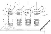
- the present inventionincludes use of a plurality of the ultra-small resonant structures that are formed in a vertically stacked array, for example as is shown in the stacked array in FIG. 3 at 50 .
- a plurality of vertical stacks, as shown at 51 - 54 , of the ultra-small resonant structurescould be arranged on a substrate 55 , with each stack being comprised of a number of component substructures 56 a , 56 b , . . . , 56 - n that are separated by layers of dielectric or insulating material 55 a , 55 b , . . . , 55 - n .
- a beam of charged particles 58for example produced from a field emission tip 57 that is energized via a conductive path 57 a , passes through the center of the stacked array, through a central cavity 59 provided in each stacked array and in proximity to the stacked ultra-small nano-resonating structures 56 a . . . 56 - n causing excitation which causes nearby structures designed to be resonant at or near the frequency of radiation to resonate and thereby to produce electromagnetic radiation (denoted E in the drawing).
- Electromagnetic radiationmay be coupled out of nano-resonating structures 56 a . . . 56 - n , .e.g., to some other structure; for example, the electromagnetic radiation may be coupled to an electromagnetic wave via a waveguide conduit, which might be, for example, an optical fiber or the like.
- a stack of the structures 110could be formed by suitable techniques, such as those noted above in the referenced applications (in particular as has been described in co-pending U.S. application Ser. Nos. 10/917,511 and Ser. No. 11/203,407, both of which were previously referenced above and incorporated herein by reference).
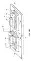
- Each vertical stack, 102 and 104could employ a plurality of vertically arranged layers 106 a , 106 b , . . . , 106 - n of ultra-small resonant structures formed on a substrate 108 together with layers of dielectric or insulating material 126 a , 126 b , . . .
- the two stacksalso include two sets of anodes 110 and 112 and 114 and 116 , with intervening layers of dielectric or insulating material 118 / 120 and 122 / 124 there between, respectively.
- a beam of charged particles 128can be produced by a source thereof such as, for example, a field emission tip 130 , positioned on a conductive region 119 , which produces the beam 128 so that it passes upwardly past the stacked array of ultra-small resonant structures 106 a . . . 106 - n so that each of the layered ultra-small resonant structures within the stack will resonate and emit EMR.
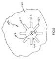
- FIG. 5shows another cross-sectional shape 150 for the ultra-small resonant structures that begins with a central cavity 152 , a central hub 154 and an exterior that has been divided into a plurality of equally spaced segments or arms 156 a , 156 b , . . . , 156 - n , when viewed in a counter clockwise direction.
- the arms 156 a - 156 - n and central portion 154can be arranged in a vertical stack, similar to that shown in FIG.
- central cavity 152being formed so as to extend down the center of the stack of ultra-small resonant structures 150 to the substrate 160 so that a field emission tip or other source of a beam of charged particles can be positioned on substrate 160 at the bottom of cavity 152 with a resulting a beam 162 being generated and sent vertically up past the individual ultra-small resonant structures 150 in the stack. That charged beam will energize the ultra-small resonant structures 150 causing them to resonate and produce EMR.
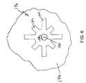
- FIG. 6shows an alternative form for the ultra-small resonant structures 170 where the outwardly extending arms have alternating lengths, some, as shown at 172 , being short while others, as shown at 174 , will be longer.
- a stacked array of these ultra-small resonant structures 170can be formed on and supported by a substrate 176 and a central cavity 178 can extend downwardly from the top of the stack to the substrate 176 so that a charged particle beam 180 can be sent upwardly past the stacked ultra-small resonant structures and cause them to resonate and emit EMR.
- ultra-small resonant structuresalso referenced herein as nano-resonating substructures
- the nano-resonating substructurescould also be C-shaped; semi-circular shaped; semi-ovular shaped; semi-rectangular shaped; and rectangular shaped.
- the nano-resonating structures discussed hereincan be constructed with many types of materials. Examples of suitable fabrication materials include silver, high conductivity metals, and high temperature superconducting materials. The material may be opaque or semi-transparent. In the above-identified patent applications, ultra-small structures for producing electromagnetic radiation are disclosed, and methods of making the same.
- the resonant structures of the present inventionare made from at least one layer of metal (e.g., silver, gold, aluminum, platinum or copper or alloys made with such metals); however, multiple layers and non-metallic structures (e.g., carbon nanotubes and high temperature superconductors) can be utilized, as long as the structures are excited by the passage of a charged particle beam.
- the materials making up the resonant structuresmay be deposited on a substrate and then etched, electroplated, or otherwise processed to create a number of individual resonant elements.
- the materialneed not even be a contiguous layer, but can be a series of resonant elements individually present on a substrate.
- the materials making up the resonant elementscan be produced by a variety of methods, such as pulsed-plating, depositing or etching. Preferred methods for doing so are described in co-pending U.S. application Ser. Nos. 10/917,511 and Ser. No. 11/203,407, both of which were previously referenced above and incorporated herein by reference.
- the construction of the vertical stacks of ultra-small resonant structurescan be manufactured by making the various layers one at a time, or the stacked layers could be formed and then the central opening could be formed as well as the final exterior shape by removing portions of the formed stack. It should also be understood that rows of vertically extending stacks, each comprised of a plurality of layered ultra-small resonant structures, can be, and are considered as, part of the invention. Such rows would then extend vertically, at about 90 degrees relative to the surface of the substrate, rather than horizontally.
- the vertically stacked arrays of ultra-small resonant structurescould also be disposed at an angle to the surface of the supporting substrate, such as, for example at an angle ranging from 1 degree to about 89 degrees, and preferably 10 degrees to about 80 degrees.
Landscapes
- Engineering & Computer Science (AREA)
- Chemical & Material Sciences (AREA)
- Nanotechnology (AREA)
- Crystallography & Structural Chemistry (AREA)
- Physics & Mathematics (AREA)
- Optics & Photonics (AREA)
- Biophysics (AREA)
- Life Sciences & Earth Sciences (AREA)
- Composite Materials (AREA)
- Condensed Matter Physics & Semiconductors (AREA)
- General Physics & Mathematics (AREA)
- Materials Engineering (AREA)
- Electron Beam Exposure (AREA)
Abstract
Description
Claims (16)
Priority Applications (1)
| Application Number | Priority Date | Filing Date | Title |
|---|---|---|---|
| US11/418,123US7728397B2 (en) | 2006-05-05 | 2006-05-05 | Coupled nano-resonating energy emitting structures |
Applications Claiming Priority (1)
| Application Number | Priority Date | Filing Date | Title |
|---|---|---|---|
| US11/418,123US7728397B2 (en) | 2006-05-05 | 2006-05-05 | Coupled nano-resonating energy emitting structures |
Publications (2)
| Publication Number | Publication Date |
|---|---|
| US20070257620A1 US20070257620A1 (en) | 2007-11-08 |
| US7728397B2true US7728397B2 (en) | 2010-06-01 |
Family
ID=38660602
Family Applications (1)
| Application Number | Title | Priority Date | Filing Date |
|---|---|---|---|
| US11/418,123Active - Reinstated2026-08-11US7728397B2 (en) | 2006-05-05 | 2006-05-05 | Coupled nano-resonating energy emitting structures |
Country Status (1)
| Country | Link |
|---|---|
| US (1) | US7728397B2 (en) |
Cited By (16)
| Publication number | Priority date | Publication date | Assignee | Title |
|---|---|---|---|---|
| US20090230332A1 (en)* | 2007-10-10 | 2009-09-17 | Virgin Islands Microsystems, Inc. | Depressed Anode With Plasmon-Enabled Devices Such As Ultra-Small Resonant Structures |
| US7990336B2 (en) | 2007-06-19 | 2011-08-02 | Virgin Islands Microsystems, Inc. | Microwave coupled excitation of solid state resonant arrays |
| US8384042B2 (en) | 2006-01-05 | 2013-02-26 | Advanced Plasmonics, Inc. | Switching micro-resonant structures by modulating a beam of charged particles |
| US8446096B1 (en)* | 2009-10-02 | 2013-05-21 | The United States Of America As Represented By The Secretary Of The Navy | Terahertz (THz) reverse micromagnetron |
| WO2013184103A1 (en)* | 2012-06-05 | 2013-12-12 | Rapiscan Systems, Inc. | Optimization of the source firing pattern for x-ray scanning systems |
| US8824637B2 (en) | 2008-09-13 | 2014-09-02 | Rapiscan Systems, Inc. | X-ray tubes |
| US9001973B2 (en) | 2003-04-25 | 2015-04-07 | Rapiscan Systems, Inc. | X-ray sources |
| US9208988B2 (en) | 2005-10-25 | 2015-12-08 | Rapiscan Systems, Inc. | Graphite backscattered electron shield for use in an X-ray tube |
| US9263225B2 (en) | 2008-07-15 | 2016-02-16 | Rapiscan Systems, Inc. | X-ray tube anode comprising a coolant tube |
| US9420677B2 (en) | 2009-01-28 | 2016-08-16 | Rapiscan Systems, Inc. | X-ray tube electron sources |
| US9726619B2 (en) | 2005-10-25 | 2017-08-08 | Rapiscan Systems, Inc. | Optimization of the source firing pattern for X-ray scanning systems |
| US10483077B2 (en) | 2003-04-25 | 2019-11-19 | Rapiscan Systems, Inc. | X-ray sources having reduced electron scattering |
| US10585206B2 (en) | 2017-09-06 | 2020-03-10 | Rapiscan Systems, Inc. | Method and system for a multi-view scanner |
| US10901112B2 (en) | 2003-04-25 | 2021-01-26 | Rapiscan Systems, Inc. | X-ray scanning system with stationary x-ray sources |
| US10976271B2 (en) | 2005-12-16 | 2021-04-13 | Rapiscan Systems, Inc. | Stationary tomographic X-ray imaging systems for automatically sorting objects based on generated tomographic images |
| US11212902B2 (en) | 2020-02-25 | 2021-12-28 | Rapiscan Systems, Inc. | Multiplexed drive systems and methods for a multi-emitter X-ray source |
Families Citing this family (3)
| Publication number | Priority date | Publication date | Assignee | Title |
|---|---|---|---|---|
| JP4063784B2 (en)* | 2003-05-15 | 2008-03-19 | シャープ株式会社 | Ion generator, ion generator |
| US8140284B2 (en)* | 2009-03-23 | 2012-03-20 | Toyota Motor Engineering & Manufacturing North America, Inc. | System for mapping vehicle mutilation defects |
| US7935930B1 (en)* | 2009-07-04 | 2011-05-03 | Jonathan Gorrell | Coupling energy from a two dimensional array of nano-resonanting structures |
Citations (317)
| Publication number | Priority date | Publication date | Assignee | Title |
|---|---|---|---|---|
| US1948384A (en) | 1932-01-26 | 1934-02-20 | Research Corp | Method and apparatus for the acceleration of ions |
| US2307086A (en) | 1941-05-07 | 1943-01-05 | Univ Leland Stanford Junior | High frequency electrical apparatus |
| US2431396A (en) | 1942-12-21 | 1947-11-25 | Rca Corp | Current magnitude-ratio responsive amplifier |
| US2473477A (en) | 1946-07-24 | 1949-06-14 | Raythcon Mfg Company | Magnetic induction device |
| US2634372A (en) | 1953-04-07 | Super high-frequency electromag | ||
| US2932798A (en) | 1956-01-05 | 1960-04-12 | Research Corp | Imparting energy to charged particles |
| US2944183A (en) | 1957-01-25 | 1960-07-05 | Bell Telephone Labor Inc | Internal cavity reflex klystron tuned by a tightly coupled external cavity |
| US2966611A (en) | 1959-07-21 | 1960-12-27 | Sperry Rand Corp | Ruggedized klystron tuner |
| US3231779A (en) | 1962-06-25 | 1966-01-25 | Gen Electric | Elastic wave responsive apparatus |
| US3274428A (en) | 1962-06-29 | 1966-09-20 | English Electric Valve Co Ltd | Travelling wave tube with band pass slow wave structure whose frequency characteristic changes along its length |
| US3297905A (en) | 1963-02-06 | 1967-01-10 | Varian Associates | Electron discharge device of particular materials for stabilizing frequency and reducing magnetic field problems |
| US3315117A (en) | 1963-07-15 | 1967-04-18 | Burton J Udelson | Electrostatically focused electron beam phase shifter |
| US3387169A (en) | 1965-05-07 | 1968-06-04 | Sfd Lab Inc | Slow wave structure of the comb type having strap means connecting the teeth to form iterative inductive shunt loadings |
| US3543147A (en) | 1968-03-29 | 1970-11-24 | Atomic Energy Commission | Phase angle measurement system for determining and controlling the resonance of the radio frequency accelerating cavities for high energy charged particle accelerators |
| US3546524A (en) | 1967-11-24 | 1970-12-08 | Varian Associates | Linear accelerator having the beam injected at a position of maximum r.f. accelerating field |
| US3560694A (en) | 1969-01-21 | 1971-02-02 | Varian Associates | Microwave applicator employing flat multimode cavity for treating webs |
| US3571642A (en) | 1968-01-17 | 1971-03-23 | Ca Atomic Energy Ltd | Method and apparatus for interleaved charged particle acceleration |
| US3586899A (en) | 1968-06-12 | 1971-06-22 | Ibm | Apparatus using smith-purcell effect for frequency modulation and beam deflection |
| US3761828A (en) | 1970-12-10 | 1973-09-25 | J Pollard | Linear particle accelerator with coast through shield |
| US3886399A (en) | 1973-08-20 | 1975-05-27 | Varian Associates | Electron beam electrical power transmission system |
| US3923568A (en) | 1974-01-14 | 1975-12-02 | Int Plasma Corp | Dry plasma process for etching noble metal |
| US3989347A (en) | 1974-06-20 | 1976-11-02 | Siemens Aktiengesellschaft | Acousto-optical data input transducer with optical data storage and process for operation thereof |
| US4053845A (en) | 1967-03-06 | 1977-10-11 | Gordon Gould | Optically pumped laser amplifiers |
| US4269672A (en) | 1979-06-01 | 1981-05-26 | Inoue-Japax Research Incorporated | Gap distance control electroplating |
| US4282436A (en) | 1980-06-04 | 1981-08-04 | The United States Of America As Represented By The Secretary Of The Navy | Intense ion beam generation with an inverse reflex tetrode (IRT) |
| US4296354A (en) | 1979-11-28 | 1981-10-20 | Varian Associates, Inc. | Traveling wave tube with frequency variable sever length |
| US4450554A (en) | 1981-08-10 | 1984-05-22 | International Telephone And Telegraph Corporation | Asynchronous integrated voice and data communication system |
| US4453108A (en) | 1980-11-21 | 1984-06-05 | William Marsh Rice University | Device for generating RF energy from electromagnetic radiation of another form such as light |
| US4482779A (en) | 1983-04-19 | 1984-11-13 | The United States Of America As Represented By The Administrator Of National Aeronautics And Space Administration | Inelastic tunnel diodes |
| US4528659A (en) | 1981-12-17 | 1985-07-09 | International Business Machines Corporation | Interleaved digital data and voice communications system apparatus and method |
| US4589107A (en) | 1982-11-30 | 1986-05-13 | Itt Corporation | Simultaneous voice and data communication and data base access in a switching system using a combined voice conference and data base processing module |
| US4598397A (en) | 1984-02-21 | 1986-07-01 | Cxc Corporation | Microtelephone controller |
| US4630262A (en) | 1984-05-23 | 1986-12-16 | International Business Machines Corp. | Method and system for transmitting digitized voice signals as packets of bits |
| US4652703A (en) | 1983-03-01 | 1987-03-24 | Racal Data Communications Inc. | Digital voice transmission having improved echo suppression |
| US4661783A (en) | 1981-03-18 | 1987-04-28 | The United States Of America As Represented By The Secretary Of The Navy | Free electron and cyclotron resonance distributed feedback lasers and masers |
| US4704583A (en) | 1974-08-16 | 1987-11-03 | Gordon Gould | Light amplifiers employing collisions to produce a population inversion |
| US4712042A (en) | 1986-02-03 | 1987-12-08 | Accsys Technology, Inc. | Variable frequency RFQ linear accelerator |
| US4713581A (en) | 1983-08-09 | 1987-12-15 | Haimson Research Corporation | Method and apparatus for accelerating a particle beam |
| US4727550A (en) | 1985-09-19 | 1988-02-23 | Chang David B | Radiation source |
| US4740963A (en) | 1986-01-30 | 1988-04-26 | Lear Siegler, Inc. | Voice and data communication system |
| US4740973A (en) | 1984-05-21 | 1988-04-26 | Madey John M J | Free electron laser |
| US4746201A (en) | 1967-03-06 | 1988-05-24 | Gordon Gould | Polarizing apparatus employing an optical element inclined at brewster's angle |
| US4761059A (en) | 1986-07-28 | 1988-08-02 | Rockwell International Corporation | External beam combining of multiple lasers |
| US4782485A (en) | 1985-08-23 | 1988-11-01 | Republic Telcom Systems Corporation | Multiplexed digital packet telephone system |
| US4789945A (en) | 1985-07-29 | 1988-12-06 | Advantest Corporation | Method and apparatus for charged particle beam exposure |
| US4806859A (en) | 1987-01-27 | 1989-02-21 | Ford Motor Company | Resonant vibrating structures with driving sensing means for noncontacting position and pick up sensing |
| US4809271A (en) | 1986-11-14 | 1989-02-28 | Hitachi, Ltd. | Voice and data multiplexer system |
| US4813040A (en) | 1986-10-31 | 1989-03-14 | Futato Steven P | Method and apparatus for transmitting digital data and real-time digitalized voice information over a communications channel |
| US4819228A (en) | 1984-10-29 | 1989-04-04 | Stratacom Inc. | Synchronous packet voice/data communication system |
| US4829527A (en) | 1984-04-23 | 1989-05-09 | The United States Of America As Represented By The Secretary Of The Army | Wideband electronic frequency tuning for orotrons |
| US4838021A (en) | 1987-12-11 | 1989-06-13 | Hughes Aircraft Company | Electrostatic ion thruster with improved thrust modulation |
| US4841538A (en) | 1986-03-05 | 1989-06-20 | Kabushiki Kaisha Toshiba | CO2 gas laser device |
| US4864131A (en) | 1987-11-09 | 1989-09-05 | The University Of Michigan | Positron microscopy |
| US4866704A (en) | 1988-03-16 | 1989-09-12 | California Institute Of Technology | Fiber optic voice/data network |
| US4866732A (en) | 1985-02-04 | 1989-09-12 | Mitel Telecom Limited | Wireless telephone system |
| US4873715A (en) | 1986-06-10 | 1989-10-10 | Hitachi, Ltd. | Automatic data/voice sending/receiving mode switching device |
| US4887265A (en) | 1988-03-18 | 1989-12-12 | Motorola, Inc. | Packet-switched cellular telephone system |
| US4890282A (en) | 1988-03-08 | 1989-12-26 | Network Equipment Technologies, Inc. | Mixed mode compression for data transmission |
| US4898022A (en) | 1987-02-09 | 1990-02-06 | Tlv Co., Ltd. | Steam trap operation detector |
| US4912705A (en) | 1985-03-20 | 1990-03-27 | International Mobile Machines Corporation | Subscriber RF telephone system for providing multiple speech and/or data signals simultaneously over either a single or a plurality of RF channels |
| US4932022A (en) | 1987-10-07 | 1990-06-05 | Telenova, Inc. | Integrated voice and data telephone system |
| US4981371A (en) | 1989-02-17 | 1991-01-01 | Itt Corporation | Integrated I/O interface for communication terminal |
| US5023563A (en) | 1989-06-08 | 1991-06-11 | Hughes Aircraft Company | Upshifted free electron laser amplifier |
| US5036513A (en) | 1989-06-21 | 1991-07-30 | Academy Of Applied Science | Method of and apparatus for integrated voice (audio) communication simultaneously with "under voice" user-transparent digital data between telephone instruments |
| US5065425A (en) | 1988-12-23 | 1991-11-12 | Telic Alcatel | Telephone connection arrangement for a personal computer and a device for such an arrangement |
| US5113141A (en) | 1990-07-18 | 1992-05-12 | Science Applications International Corporation | Four-fingers RFQ linac structure |
| US5121385A (en) | 1988-09-14 | 1992-06-09 | Fujitsu Limited | Highly efficient multiplexing system |
| US5127001A (en) | 1990-06-22 | 1992-06-30 | Unisys Corporation | Conference call arrangement for distributed network |
| US5128729A (en) | 1990-11-13 | 1992-07-07 | Motorola, Inc. | Complex opto-isolator with improved stand-off voltage stability |
| US5130985A (en) | 1988-11-25 | 1992-07-14 | Hitachi, Ltd. | Speech packet communication system and method |
| US5150410A (en) | 1991-04-11 | 1992-09-22 | Itt Corporation | Secure digital conferencing system |
| US5155726A (en) | 1990-01-22 | 1992-10-13 | Digital Equipment Corporation | Station-to-station full duplex communication in a token ring local area network |
| US5157000A (en) | 1989-07-10 | 1992-10-20 | Texas Instruments Incorporated | Method for dry etching openings in integrated circuit layers |
| US5163118A (en) | 1986-11-10 | 1992-11-10 | The United States Of America As Represented By The Secretary Of The Air Force | Lattice mismatched hetrostructure optical waveguide |
| US5185073A (en) | 1988-06-21 | 1993-02-09 | International Business Machines Corporation | Method of fabricating nendritic materials |
| US5187591A (en) | 1991-01-24 | 1993-02-16 | Micom Communications Corp. | System for transmitting and receiving aural information and modulated data |
| US5199918A (en) | 1991-11-07 | 1993-04-06 | Microelectronics And Computer Technology Corporation | Method of forming field emitter device with diamond emission tips |
| US5214650A (en) | 1990-11-19 | 1993-05-25 | Ag Communication Systems Corporation | Simultaneous voice and data system using the existing two-wire inter-face |
| US5233623A (en) | 1992-04-29 | 1993-08-03 | Research Foundation Of State University Of New York | Integrated semiconductor laser with electronic directivity and focusing control |
| US5235248A (en) | 1990-06-08 | 1993-08-10 | The United States Of America As Represented By The United States Department Of Energy | Method and split cavity oscillator/modulator to generate pulsed particle beams and electromagnetic fields |
| WO1993021663A1 (en) | 1992-04-08 | 1993-10-28 | Georgia Tech Research Corporation | Process for lift-off of thin film materials from a growth substrate |
| US5263043A (en) | 1990-08-31 | 1993-11-16 | Trustees Of Dartmouth College | Free electron laser utilizing grating coupling |
| US5262656A (en) | 1991-06-07 | 1993-11-16 | Thomson-Csf | Optical semiconductor transceiver with chemically resistant layers |
| US5268693A (en) | 1990-08-31 | 1993-12-07 | Trustees Of Dartmouth College | Semiconductor film free electron laser |
| US5268788A (en) | 1991-06-25 | 1993-12-07 | Smiths Industries Public Limited Company | Display filter arrangements |
| US5282197A (en) | 1992-05-15 | 1994-01-25 | International Business Machines | Low frequency audio sub-channel embedded signalling |
| US5283819A (en) | 1991-04-25 | 1994-02-01 | Compuadd Corporation | Computing and multimedia entertainment system |
| US5293175A (en) | 1991-07-19 | 1994-03-08 | Conifer Corporation | Stacked dual dipole MMDS feed |
| US5302240A (en) | 1991-01-22 | 1994-04-12 | Kabushiki Kaisha Toshiba | Method of manufacturing semiconductor device |
| US5305312A (en) | 1992-02-07 | 1994-04-19 | At&T Bell Laboratories | Apparatus for interfacing analog telephones and digital data terminals to an ISDN line |
| US5341374A (en) | 1991-03-01 | 1994-08-23 | Trilan Systems Corporation | Communication network integrating voice data and video with distributed call processing |
| US5446814A (en) | 1993-11-05 | 1995-08-29 | Motorola | Molded reflective optical waveguide |
| US5485277A (en) | 1994-07-26 | 1996-01-16 | Physical Optics Corporation | Surface plasmon resonance sensor and methods for the utilization thereof |
| US5504341A (en) | 1995-02-17 | 1996-04-02 | Zimec Consulting, Inc. | Producing RF electric fields suitable for accelerating atomic and molecular ions in an ion implantation system |
| US5578909A (en) | 1994-07-15 | 1996-11-26 | The Regents Of The Univ. Of California | Coupled-cavity drift-tube linac |
| US5604352A (en) | 1995-04-25 | 1997-02-18 | Raychem Corporation | Apparatus comprising voltage multiplication components |
| US5608263A (en) | 1994-09-06 | 1997-03-04 | The Regents Of The University Of Michigan | Micromachined self packaged circuits for high-frequency applications |
| US5637966A (en) | 1995-02-06 | 1997-06-10 | The Regents Of The University Of Michigan | Method for generating a plasma wave to accelerate electrons |
| US5663971A (en) | 1996-04-02 | 1997-09-02 | The Regents Of The University Of California, Office Of Technology Transfer | Axial interaction free-electron laser |
| US5666020A (en) | 1994-11-16 | 1997-09-09 | Nec Corporation | Field emission electron gun and method for fabricating the same |
| US5668368A (en) | 1992-02-21 | 1997-09-16 | Hitachi, Ltd. | Apparatus for suppressing electrification of sample in charged beam irradiation apparatus |
| US5705443A (en) | 1995-05-30 | 1998-01-06 | Advanced Technology Materials, Inc. | Etching method for refractory materials |
| US5737458A (en) | 1993-03-29 | 1998-04-07 | Martin Marietta Corporation | Optical light pipe and microwave waveguide interconnects in multichip modules formed using adaptive lithography |
| US5744919A (en) | 1996-12-12 | 1998-04-28 | Mishin; Andrey V. | CW particle accelerator with low particle injection velocity |
| US5757009A (en) | 1996-12-27 | 1998-05-26 | Northrop Grumman Corporation | Charged particle beam expander |
| US5767013A (en) | 1996-08-26 | 1998-06-16 | Lg Semicon Co., Ltd. | Method for forming interconnection in semiconductor pattern device |
| US5780970A (en) | 1996-10-28 | 1998-07-14 | University Of Maryland | Multi-stage depressed collector for small orbit gyrotrons |
| US5790585A (en) | 1996-11-12 | 1998-08-04 | The Trustees Of Dartmouth College | Grating coupling free electron laser apparatus and method |
| US5811943A (en) | 1996-09-23 | 1998-09-22 | Schonberg Research Corporation | Hollow-beam microwave linear accelerator |
| US5821902A (en) | 1993-09-02 | 1998-10-13 | Inmarsat | Folded dipole microstrip antenna |
| US5821836A (en) | 1997-05-23 | 1998-10-13 | The Regents Of The University Of Michigan | Miniaturized filter assembly |
| US5825140A (en) | 1996-02-29 | 1998-10-20 | Nissin Electric Co., Ltd. | Radio-frequency type charged particle accelerator |
| US5831270A (en) | 1996-02-19 | 1998-11-03 | Nikon Corporation | Magnetic deflectors and charged-particle-beam lithography systems incorporating same |
| US5847745A (en) | 1995-03-03 | 1998-12-08 | Futaba Denshi Kogyo K.K. | Optical write element |
| US5858799A (en) | 1995-10-25 | 1999-01-12 | University Of Washington | Surface plasmon resonance chemical electrode |
| US5889449A (en) | 1995-12-07 | 1999-03-30 | Space Systems/Loral, Inc. | Electromagnetic transmission line elements having a boundary between materials of high and low dielectric constants |
| US5889797A (en) | 1996-08-26 | 1999-03-30 | The Regents Of The University Of California | Measuring short electron bunch lengths using coherent smith-purcell radiation |
| US5902489A (en) | 1995-11-08 | 1999-05-11 | Hitachi, Ltd. | Particle handling method by acoustic radiation force and apparatus therefore |
| US5963857A (en) | 1998-01-20 | 1999-10-05 | Lucent Technologies, Inc. | Article comprising a micro-machined filter |
| US5972193A (en) | 1997-10-10 | 1999-10-26 | Industrial Technology Research Institute | Method of manufacturing a planar coil using a transparency substrate |
| US6005347A (en) | 1995-12-12 | 1999-12-21 | Lg Electronics Inc. | Cathode for a magnetron having primary and secondary electron emitters |
| US6008496A (en) | 1997-05-05 | 1999-12-28 | University Of Florida | High resolution resonance ionization imaging detector and method |
| US6040625A (en) | 1997-09-25 | 2000-03-21 | I/O Sensors, Inc. | Sensor package arrangement |
| US6060833A (en) | 1996-10-18 | 2000-05-09 | Velazco; Jose E. | Continuous rotating-wave electron beam accelerator |
| US6080529A (en) | 1997-12-12 | 2000-06-27 | Applied Materials, Inc. | Method of etching patterned layers useful as masking during subsequent etching or for damascene structures |
| US6117784A (en) | 1997-11-12 | 2000-09-12 | International Business Machines Corporation | Process for integrated circuit wiring |
| US6139760A (en)* | 1997-12-19 | 2000-10-31 | Electronics And Telecommunications Research Institute | Short-wavelength optoelectronic device including field emission device and its fabricating method |
| US6180415B1 (en) | 1997-02-20 | 2001-01-30 | The Regents Of The University Of California | Plasmon resonant particles, methods and apparatus |
| US6195199B1 (en) | 1997-10-27 | 2001-02-27 | Kanazawa University | Electron tube type unidirectional optical amplifier |
| US6210555B1 (en) | 1999-01-29 | 2001-04-03 | Faraday Technology Marketing Group, Llc | Electrodeposition of metals in small recesses for manufacture of high density interconnects using reverse pulse plating |
| US6222866B1 (en) | 1997-01-06 | 2001-04-24 | Fuji Xerox Co., Ltd. | Surface emitting semiconductor laser, its producing method and surface emitting semiconductor laser array |
| US6278239B1 (en) | 1996-06-25 | 2001-08-21 | The United States Of America As Represented By The United States Department Of Energy | Vacuum-surface flashover switch with cantilever conductors |
| US6297511B1 (en) | 1999-04-01 | 2001-10-02 | Raytheon Company | High frequency infrared emitter |
| US20010025925A1 (en) | 2000-03-28 | 2001-10-04 | Kabushiki Kaisha Toshiba | Charged particle beam system and pattern slant observing method |
| US6301041B1 (en) | 1998-08-18 | 2001-10-09 | Kanazawa University | Unidirectional optical amplifier |
| US6303014B1 (en) | 1998-10-14 | 2001-10-16 | Faraday Technology Marketing Group, Llc | Electrodeposition of metals in small recesses using modulated electric fields |
| US6309528B1 (en) | 1999-10-15 | 2001-10-30 | Faraday Technology Marketing Group, Llc | Sequential electrodeposition of metals using modulated electric fields for manufacture of circuit boards having features of different sizes |
| US6316876B1 (en) | 1998-08-19 | 2001-11-13 | Eiji Tanabe | High gradient, compact, standing wave linear accelerator structure |
| US20010045360A1 (en) | 2000-05-25 | 2001-11-29 | Ryushin Omasa | Electroplating method using combination of vibrational flow in plating bath and plating current of pulse |
| US6338968B1 (en) | 1998-02-02 | 2002-01-15 | Signature Bioscience, Inc. | Method and apparatus for detecting molecular binding events |
| US20020036264A1 (en) | 2000-07-27 | 2002-03-28 | Mamoru Nakasuji | Sheet beam-type inspection apparatus |
| US20020036121A1 (en) | 2000-09-08 | 2002-03-28 | Ronald Ball | Illumination system for escalator handrails |
| US6370306B1 (en) | 1997-12-15 | 2002-04-09 | Seiko Instruments Inc. | Optical waveguide probe and its manufacturing method |
| US6373194B1 (en) | 2000-06-01 | 2002-04-16 | Raytheon Company | Optical magnetron for high efficiency production of optical radiation |
| US20020053638A1 (en) | 1998-07-03 | 2002-05-09 | Dieter Winkler | Apparatus and method for examing specimen with a charged particle beam |
| US20020056645A1 (en) | 1998-10-14 | 2002-05-16 | Taylor E. Jennings | Electrodeposition of metals in small recesses using modulated electric fields |
| US20020068018A1 (en) | 2000-12-06 | 2002-06-06 | Hrl Laboratories, Llc | Compact sensor using microcavity structures |
| US20020071457A1 (en) | 2000-12-08 | 2002-06-13 | Hogan Josh N. | Pulsed non-linear resonant cavity |
| US6407516B1 (en) | 2000-05-26 | 2002-06-18 | Exaconnect Inc. | Free space electron switch |
| US6441298B1 (en) | 2000-08-15 | 2002-08-27 | Nec Research Institute, Inc | Surface-plasmon enhanced photovoltaic device |
| US20020122531A1 (en) | 2001-03-05 | 2002-09-05 | Siemens Medical Systems, Inc. | Multi-mode operation of a standing wave linear accelerator |
| US6448850B1 (en) | 1999-05-20 | 2002-09-10 | Kanazawa University | Electromagnetic wave amplifier and electromagnetic wave generator |
| US6453087B2 (en) | 2000-04-28 | 2002-09-17 | Confluent Photonics Co. | Miniature monolithic optical add-drop multiplexer |
| US20020135665A1 (en) | 2001-03-20 | 2002-09-26 | Keith Gardner | Led print head for electrophotographic printer |
| US20020139961A1 (en) | 2001-03-23 | 2002-10-03 | Fuji Photo Film Co., Ltd. | Molecular electric wire, molecular electric wire circuit using the same and process for producing the molecular electric wire circuit |
| US6470198B1 (en) | 1999-04-28 | 2002-10-22 | Murata Manufacturing Co., Ltd. | Electronic part, dielectric resonator, dielectric filter, duplexer, and communication device comprised of high TC superconductor |
| US20020158295A1 (en) | 2001-03-07 | 2002-10-31 | Marten Armgarth | Electrochemical device |
| US20020191650A1 (en) | 2001-02-26 | 2002-12-19 | Madey John M. J. | Phase displacement free-electron laser |
| US20030012925A1 (en) | 2001-07-16 | 2003-01-16 | Motorola, Inc. | Process for fabricating semiconductor structures and devices utilizing the formation of a compliant substrate for materials used to form the same and including an etch stop layer used for back side processing |
| US20030010979A1 (en) | 2000-01-14 | 2003-01-16 | Fabrice Pardo | Vertical metal-semiconductor microresonator photodetecting device and production method thereof |
| US20030016421A1 (en) | 2000-06-01 | 2003-01-23 | Small James G. | Wireless communication system with high efficiency/high power optical source |
| US20030034535A1 (en) | 2001-08-15 | 2003-02-20 | Motorola, Inc. | Mems devices suitable for integration with chip having integrated silicon and compound semiconductor devices, and methods for fabricating such devices |
| US6525477B2 (en) | 2001-05-29 | 2003-02-25 | Raytheon Company | Optical magnetron generator |
| US6545425B2 (en) | 2000-05-26 | 2003-04-08 | Exaconnect Corp. | Use of a free space electron switch in a telecommunications network |
| US6552320B1 (en) | 1999-06-21 | 2003-04-22 | United Microelectronics Corp. | Image sensor structure |
| US20030103150A1 (en) | 2001-11-30 | 2003-06-05 | Catrysse Peter B. | Integrated color pixel ( ICP ) |
| US6577040B2 (en) | 1999-01-14 | 2003-06-10 | The Regents Of The University Of Michigan | Method and apparatus for generating a signal having at least one desired output frequency utilizing a bank of vibrating micromechanical devices |
| US20030106998A1 (en) | 1996-08-08 | 2003-06-12 | William Marsh Rice University | Method for producing boron nitride coatings and fibers and compositions thereof |
| US6580075B2 (en) | 1998-09-18 | 2003-06-17 | Hitachi, Ltd. | Charged particle beam scanning type automatic inspecting apparatus |
| US6603915B2 (en) | 2001-02-05 | 2003-08-05 | Fujitsu Limited | Interposer and method for producing a light-guiding structure |
| US6603781B1 (en) | 2001-01-19 | 2003-08-05 | Siros Technologies, Inc. | Multi-wavelength transmitter |
| US20030155521A1 (en) | 2000-02-01 | 2003-08-21 | Hans-Peter Feuerbaum | Optical column for charged particle beam device |
| US20030158474A1 (en) | 2002-01-18 | 2003-08-21 | Axel Scherer | Method and apparatus for nanomagnetic manipulation and sensing |
| US20030164947A1 (en) | 2000-04-18 | 2003-09-04 | Matthias Vaupel | Spr sensor |
| US6624916B1 (en) | 1997-02-11 | 2003-09-23 | Quantumbeam Limited | Signalling system |
| US20030179974A1 (en) | 2002-03-20 | 2003-09-25 | Estes Michael J. | Surface plasmon devices |
| US6636185B1 (en) | 1992-03-13 | 2003-10-21 | Kopin Corporation | Head-mounted display system |
| US6636653B2 (en) | 2001-02-02 | 2003-10-21 | Teravicta Technologies, Inc. | Integrated optical micro-electromechanical systems and methods of fabricating and operating the same |
| US6640023B2 (en) | 2001-09-27 | 2003-10-28 | Memx, Inc. | Single chip optical cross connect |
| US6642907B2 (en) | 2001-01-12 | 2003-11-04 | The Furukawa Electric Co., Ltd. | Antenna device |
| US20030206708A1 (en) | 2002-03-20 | 2003-11-06 | Estes Michael J. | Surface plasmon devices |
| US20030214695A1 (en) | 2002-03-18 | 2003-11-20 | E Ink Corporation | Electro-optic displays, and methods for driving same |
| US20030222579A1 (en) | 2001-11-13 | 2003-12-04 | Burle Technologies, Inc. | Photocathode |
| US20040011432A1 (en) | 2002-07-17 | 2004-01-22 | Podlaha Elizabeth J. | Metal alloy electrodeposited microstructures |
| US6687034B2 (en) | 2001-03-23 | 2004-02-03 | Microvision, Inc. | Active tuning of a torsional resonant structure |
| US6700748B1 (en) | 2000-04-28 | 2004-03-02 | International Business Machines Corporation | Methods for creating ground paths for ILS |
| US20040061053A1 (en) | 2001-02-28 | 2004-04-01 | Yoshifumi Taniguchi | Method and apparatus for measuring physical properties of micro region |
| US6724486B1 (en) | 1999-04-28 | 2004-04-20 | Zygo Corporation | Helium- Neon laser light source generating two harmonically related, single- frequency wavelengths for use in displacement and dispersion measuring interferometry |
| US20040080285A1 (en) | 2000-05-26 | 2004-04-29 | Victor Michel N. | Use of a free space electron switch in a telecommunications network |
| US20040085159A1 (en) | 2002-11-01 | 2004-05-06 | Kubena Randall L. | Micro electrical mechanical system (MEMS) tuning using focused ion beams |
| US20040092104A1 (en) | 2002-06-19 | 2004-05-13 | Luxtera, Inc. | Methods of incorporating germanium within CMOS process |
| US6738176B2 (en) | 2002-04-30 | 2004-05-18 | Mario Rabinowitz | Dynamic multi-wavelength switching ensemble |
| US6741781B2 (en) | 2000-09-29 | 2004-05-25 | Kabushiki Kaisha Toshiba | Optical interconnection circuit board and manufacturing method thereof |
| US20040108473A1 (en) | 2000-06-09 | 2004-06-10 | Melnychuk Stephan T. | Extreme ultraviolet light source |
| US20040108823A1 (en) | 2002-12-09 | 2004-06-10 | Fondazione Per Adroterapia Oncologica - Tera | Linac for ion beam acceleration |
| US20040108471A1 (en) | 2002-09-26 | 2004-06-10 | Chiyan Luo | Photonic crystals: a medium exhibiting anomalous cherenkov radiation |
| US20040136715A1 (en) | 2002-12-06 | 2004-07-15 | Seiko Epson Corporation | Wavelength multiplexing on-chip optical interconnection circuit, electro-optical device, and electronic apparatus |
| US20040150991A1 (en) | 2003-01-27 | 2004-08-05 | 3M Innovative Properties Company | Phosphor based light sources utilizing total internal reflection |
| US20040154925A1 (en) | 2003-02-11 | 2004-08-12 | Podlaha Elizabeth J. | Composite metal and composite metal alloy microstructures |
| US6782205B2 (en) | 2001-06-25 | 2004-08-24 | Silicon Light Machines | Method and apparatus for dynamic equalization in wavelength division multiplexing |
| US20040171272A1 (en) | 2003-02-28 | 2004-09-02 | Applied Materials, Inc. | Method of etching metallic materials to form a tapered profile |
| US6791438B2 (en) | 2001-10-30 | 2004-09-14 | Matsushita Electric Industrial Co., Ltd. | Radio frequency module and method for manufacturing the same |
| US20040180244A1 (en) | 2003-01-24 | 2004-09-16 | Tour James Mitchell | Process and apparatus for microwave desorption of elements or species from carbon nanotubes |
| US20040184270A1 (en) | 2003-03-17 | 2004-09-23 | Halter Michael A. | LED light module with micro-reflector cavities |
| US6800877B2 (en) | 2000-05-26 | 2004-10-05 | Exaconnect Corp. | Semi-conductor interconnect using free space electron switch |
| US20040213375A1 (en) | 2003-04-25 | 2004-10-28 | Paul Bjorkholm | Radiation sources and radiation scanning systems with improved uniformity of radiation intensity |
| US20040218651A1 (en) | 2000-03-03 | 2004-11-04 | Canon Kabushiki Kaisha | Electron-beam excitation laser |
| US20040217297A1 (en) | 2000-12-01 | 2004-11-04 | Yeda Research And Development Co. Ltd. | Device and method for the examination of samples in a non vacuum environment using a scanning electron microscope |
| US6819432B2 (en) | 2001-03-14 | 2004-11-16 | Hrl Laboratories, Llc | Coherent detecting receiver using a time delay interferometer and adaptive beam combiner |
| US20040231996A1 (en) | 2003-05-20 | 2004-11-25 | Novellus Systems, Inc. | Electroplating using DC current interruption and variable rotation rate |
| US20040240035A1 (en) | 2003-05-29 | 2004-12-02 | Stanislav Zhilkov | Method of modulation and electron modulator for optical communication and data transmission |
| US6829286B1 (en) | 2000-05-26 | 2004-12-07 | Opticomp Corporation | Resonant cavity enhanced VCSEL/waveguide grating coupler |
| US6834152B2 (en) | 2001-09-10 | 2004-12-21 | California Institute Of Technology | Strip loaded waveguide with low-index transition layer |
| US20040264867A1 (en) | 2002-12-06 | 2004-12-30 | Seiko Epson Corporation | Optical interconnection circuit among wavelength multiplexing chips, electro-optical device, and electronic apparatus |
| US20050023145A1 (en) | 2003-05-07 | 2005-02-03 | Microfabrica Inc. | Methods and apparatus for forming multi-layer structures using adhered masks |
| WO2005015143A2 (en) | 2003-08-11 | 2005-02-17 | Opgal Ltd. | Radiometry using an uncooled microbolometer detector |
| US20050045821A1 (en) | 2003-04-22 | 2005-03-03 | Nobuharu Noji | Testing apparatus using charged particles and device manufacturing method using the testing apparatus |
| US20050045832A1 (en) | 2003-07-11 | 2005-03-03 | Kelly Michael A. | Non-dispersive charged particle energy analyzer |
| US20050054151A1 (en) | 2002-01-04 | 2005-03-10 | Intersil Americas Inc. | Symmetric inducting device for an integrated circuit having a ground shield |
| US6870438B1 (en) | 1999-11-10 | 2005-03-22 | Kyocera Corporation | Multi-layered wiring board for slot coupling a transmission line to a waveguide |
| US6871025B2 (en) | 2000-06-15 | 2005-03-22 | California Institute Of Technology | Direct electrical-to-optical conversion and light modulation in micro whispering-gallery-mode resonators |
| US20050062903A1 (en) | 2003-09-23 | 2005-03-24 | Eastman Kodak Company | Organic laser and liquid crystal display |
| US20050067286A1 (en) | 2003-09-26 | 2005-03-31 | The University Of Cincinnati | Microfabricated structures and processes for manufacturing same |
| US20050082469A1 (en) | 1997-06-19 | 2005-04-21 | European Organization For Nuclear Research | Neutron-driven element transmuter |
| US6885262B2 (en) | 2002-11-05 | 2005-04-26 | Ube Industries, Ltd. | Band-pass filter using film bulk acoustic resonator |
| US20050092929A1 (en) | 2003-07-08 | 2005-05-05 | Schneiker Conrad W. | Integrated sub-nanometer-scale electron beam systems |
| US20050104684A1 (en) | 2003-10-03 | 2005-05-19 | Applied Materials, Inc. | Planar integrated circuit including a plasmon waveguide-fed schottky barrier detector and transistors connected therewith |
| US20050105595A1 (en) | 2003-11-17 | 2005-05-19 | Martin Frederick L. | Communication device |
| US20050105690A1 (en) | 2003-11-19 | 2005-05-19 | Stanley Pau | Focusable and steerable micro-miniature x-ray apparatus |
| US6900447B2 (en) | 2002-08-07 | 2005-05-31 | Fei Company | Focused ion beam system with coaxial scanning electron microscope |
| US6909104B1 (en) | 1999-05-25 | 2005-06-21 | Nawotec Gmbh | Miniaturized terahertz radiation source |
| US6909092B2 (en) | 2002-05-16 | 2005-06-21 | Ebara Corporation | Electron beam apparatus and device manufacturing method using same |
| US20050145882A1 (en) | 2002-10-25 | 2005-07-07 | Taylor Geoff W. | Semiconductor devices employing at least one modulation doped quantum well structure and one or more etch stop layers for accurate contact formation |
| US20050152635A1 (en) | 2001-04-05 | 2005-07-14 | Luxtera, Inc | Photonic input/output port |
| US20050162104A1 (en) | 2000-05-26 | 2005-07-28 | Victor Michel N. | Semi-conductor interconnect using free space electron switch |
| US20050180678A1 (en) | 2004-02-18 | 2005-08-18 | Panepucci Roberto R. | Optical waveguide displacement sensor |
| US6936981B2 (en) | 2002-11-08 | 2005-08-30 | Applied Materials, Inc. | Retarding electron beams in multiple electron beam pattern generation |
| US20050191055A1 (en) | 2004-02-27 | 2005-09-01 | Fujitsu Limited | Arrayed wavelength converter |
| US20050190637A1 (en) | 2003-02-06 | 2005-09-01 | Kabushiki Kaisha Toshiba | Quantum memory and information processing method using the same |
| US20050194258A1 (en) | 2003-06-27 | 2005-09-08 | Microfabrica Inc. | Electrochemical fabrication methods incorporating dielectric materials and/or using dielectric substrates |
| US6944369B2 (en) | 2001-05-17 | 2005-09-13 | Sioptical, Inc. | Optical coupler having evanescent coupling region |
| US6943650B2 (en) | 2003-05-29 | 2005-09-13 | Freescale Semiconductor, Inc. | Electromagnetic band gap microwave filter |
| US20050201717A1 (en) | 2004-03-11 | 2005-09-15 | Sony Corporation | Surface plasmon resonance device |
| US20050201707A1 (en) | 2004-03-12 | 2005-09-15 | Alexei Glebov | Flexible optical waveguides for backplane optical interconnections |
| US20050212503A1 (en) | 2004-03-26 | 2005-09-29 | Deibele Craig E | Fast faraday cup with high bandwidth |
| US6952492B2 (en) | 2001-06-20 | 2005-10-04 | Hitachi, Ltd. | Method and apparatus for inspecting a semiconductor device |
| US6953291B2 (en) | 2003-06-30 | 2005-10-11 | Finisar Corporation | Compact package design for vertical cavity surface emitting laser array to optical fiber cable connection |
| US20050231138A1 (en) | 2004-04-19 | 2005-10-20 | Mitsubishi Denki Kabushiki Kaisha | Charged-particle beam accelerator, particle beam radiation therapy system using the charged-particle beam accelerator, and method of operating the particle beam radiation therapy system |
| US20050249451A1 (en) | 2004-04-27 | 2005-11-10 | Tom Baehr-Jones | Integrated plasmon and dielectric waveguides |
| US6965625B2 (en) | 2000-09-22 | 2005-11-15 | Vermont Photonics, Inc. | Apparatuses and methods for generating coherent electromagnetic laser radiation |
| US6965284B2 (en) | 2001-03-02 | 2005-11-15 | Matsushita Electric Industrial Co., Ltd. | Dielectric filter, antenna duplexer |
| US6972439B1 (en) | 2004-05-27 | 2005-12-06 | Samsung Electro-Mechanics Co., Ltd. | Light emitting diode device |
| US20050285541A1 (en) | 2003-06-23 | 2005-12-29 | Lechevalier Robert E | Electron beam RF amplifier and emitter |
| US20060007730A1 (en) | 2002-11-26 | 2006-01-12 | Kabushiki Kaisha Toshiba | Magnetic cell and magnetic memory |
| US20060018619A1 (en) | 2004-06-18 | 2006-01-26 | Helffrich Jerome A | System and Method for Detection of Fiber Optic Cable Using Static and Induced Charge |
| US6995406B2 (en) | 2002-06-10 | 2006-02-07 | Tsuyoshi Tojo | Multibeam semiconductor laser, semiconductor light-emitting device and semiconductor device |
| US20060035173A1 (en) | 2004-08-13 | 2006-02-16 | Mark Davidson | Patterning thin metal films by dry reactive ion etching |
| US20060045418A1 (en) | 2004-08-25 | 2006-03-02 | Information And Communication University Research And Industrial Cooperation Group | Optical printed circuit board and optical interconnection block using optical fiber bundle |
| US20060050269A1 (en) | 2002-09-27 | 2006-03-09 | Brownell James H | Free electron laser, and associated components and methods |
| US20060062258A1 (en) | 2004-07-02 | 2006-03-23 | Vanderbilt University | Smith-Purcell free electron laser and method of operating same |
| US20060060782A1 (en) | 2004-06-16 | 2006-03-23 | Anjam Khursheed | Scanning electron microscope |
| WO2006042239A2 (en) | 2004-10-06 | 2006-04-20 | The Regents Of The University Of California | Cascaded cavity silicon raman laser with electrical modulation, switching, and active mode locking capability |
| US20060131176A1 (en) | 2004-12-21 | 2006-06-22 | Shih-Ping Hsu | Multi-layer circuit board with fine pitches and fabricating method thereof |
| US20060131695A1 (en) | 2004-12-22 | 2006-06-22 | Kuekes Philip J | Fabricating arrays of metallic nanostructures |
| US7068948B2 (en) | 2001-06-13 | 2006-06-27 | Gazillion Bits, Inc. | Generation of optical signals with return-to-zero format |
| US20060159131A1 (en) | 2005-01-20 | 2006-07-20 | Ansheng Liu | Digital signal regeneration, reshaping and wavelength conversion using an optical bistable silicon Raman laser |
| US20060164496A1 (en) | 2005-01-21 | 2006-07-27 | Konica Minolta Business Technologies, Inc. | Image forming method and image forming apparatus |
| US7092603B2 (en) | 2004-03-03 | 2006-08-15 | Fujitsu Limited | Optical bridge for chip-to-board interconnection and methods of fabrication |
| US7092588B2 (en) | 2002-11-20 | 2006-08-15 | Seiko Epson Corporation | Optical interconnection circuit between chips, electrooptical device and electronic equipment |
| US20060187794A1 (en) | 2004-10-14 | 2006-08-24 | Tim Harvey | Uses of wave guided miniature holographic system |
| US7099586B2 (en) | 2003-09-04 | 2006-08-29 | The Regents Of The University Of California | Reconfigurable multi-channel all-optical regenerators |
| US20060208667A1 (en) | 2001-03-13 | 2006-09-21 | Color Kinetics Incorporated | Methods and apparatus for providing power to lighting devices |
| US20060216940A1 (en) | 2004-08-13 | 2006-09-28 | Virgin Islands Microsystems, Inc. | Methods of producing structures for electron beam induced resonance using plating and/or etching |
| US7120332B1 (en) | 2005-03-31 | 2006-10-10 | Eastman Kodak Company | Placement of lumiphores within a light emitting resonator in a visual display with electro-optical addressing architecture |
| US20060232364A1 (en) | 2002-11-07 | 2006-10-19 | Sophia Wireless,Inc. | Coupled resonator filters formed by micromachining |
| US7130102B2 (en) | 2004-07-19 | 2006-10-31 | Mario Rabinowitz | Dynamic reflection, illumination, and projection |
| US20060243925A1 (en) | 2005-05-02 | 2006-11-02 | Raytheon Company | Smith-Purcell radiation source using negative-index metamaterial (NIM) |
| US20060274922A1 (en) | 2004-04-20 | 2006-12-07 | Bio-Rad Laboratories, Inc. | Imaging method and apparatus |
| US20070003781A1 (en) | 2005-06-30 | 2007-01-04 | De Rochemont L P | Electrical components and method of manufacture |
| US20070013765A1 (en) | 2005-07-18 | 2007-01-18 | Eastman Kodak Company | Flexible organic laser printer |
| US7194798B2 (en) | 2004-06-30 | 2007-03-27 | Hitachi Global Storage Technologies Netherlands B.V. | Method for use in making a write coil of magnetic head |
| US20070075263A1 (en) | 2005-09-30 | 2007-04-05 | Virgin Islands Microsystems, Inc. | Ultra-small resonating charged particle beam modulator |
| US20070086915A1 (en) | 2005-10-14 | 2007-04-19 | General Electric Company | Detection apparatus and associated method |
| US7230201B1 (en) | 2000-02-25 | 2007-06-12 | Npl Associates | Apparatus and methods for controlling charged particles |
| US20070146704A1 (en) | 2005-12-22 | 2007-06-28 | Palo Alto Research Center Incorporated | Sensing photon energies emanating from channels or moving objects |
| US20070152176A1 (en) | 2006-01-05 | 2007-07-05 | Virgin Islands Microsystems, Inc. | Selectable frequency light emitter |
| US20070154846A1 (en) | 2006-01-05 | 2007-07-05 | Virgin Islands Microsystems, Inc. | Switching micro-resonant structures using at least one director |
| US20070194357A1 (en) | 2004-04-05 | 2007-08-23 | Keishi Oohashi | Photodiode and method for fabricating same |
| US20070200940A1 (en) | 2006-02-28 | 2007-08-30 | Gruhlke Russell W | Vertical tri-color sensor |
| US7267461B2 (en) | 2004-01-28 | 2007-09-11 | Tir Systems, Ltd. | Directly viewable luminaire |
| US7267459B2 (en) | 2004-01-28 | 2007-09-11 | Tir Systems Ltd. | Sealed housing unit for lighting system |
| US20070238037A1 (en) | 2006-03-30 | 2007-10-11 | Asml Netherlands B.V. | Imprint lithography |
| US20070252983A1 (en) | 2006-04-27 | 2007-11-01 | Tong William M | Analyte stages including tunable resonant cavities and Raman signal-enhancing structures |
| US20070258689A1 (en) | 2006-05-05 | 2007-11-08 | Virgin Islands Microsystems, Inc. | Coupling electromagnetic wave through microcircuit |
| US20070258720A1 (en) | 2006-05-05 | 2007-11-08 | Virgin Islands Microsystems, Inc. | Inter-chip optical communication |
| US20070259641A1 (en) | 2006-05-05 | 2007-11-08 | Virgin Islands Microsystems, Inc. | Heterodyne receiver array using resonant structures |
| US20070258492A1 (en) | 2006-05-05 | 2007-11-08 | Virgin Islands Microsystems, Inc. | Light-emitting resonant structure driving raman laser |
| US20070258690A1 (en) | 2006-05-05 | 2007-11-08 | Virgin Islands Microsystems, Inc. | Integration of electromagnetic detector on integrated chip |
| US20070264023A1 (en) | 2006-04-26 | 2007-11-15 | Virgin Islands Microsystems, Inc. | Free space interchip communications |
| US20070264030A1 (en) | 2006-04-26 | 2007-11-15 | Virgin Islands Microsystems, Inc. | Selectable frequency EMR emitter |
| US20070282030A1 (en) | 2003-12-05 | 2007-12-06 | Anderson Mark T | Process for Producing Photonic Crystals and Controlled Defects Therein |
| US20070284527A1 (en) | 2005-07-08 | 2007-12-13 | Zani Michael J | Apparatus and method for controlled particle beam manufacturing |
| US7309953B2 (en) | 2005-01-24 | 2007-12-18 | Principia Lightworks, Inc. | Electron beam pumped laser light source for projection television |
| US20080069509A1 (en) | 2006-09-19 | 2008-03-20 | Virgin Islands Microsystems, Inc. | Microcircuit using electromagnetic wave routing |
| US7362972B2 (en) | 2003-09-29 | 2008-04-22 | Jds Uniphase Inc. | Laser transmitter capable of transmitting line data and supervisory information at a plurality of data rates |
| US7375631B2 (en) | 2004-07-26 | 2008-05-20 | Lenovo (Singapore) Pte. Ltd. | Enabling and disabling a wireless RFID portable transponder |
| US20080218102A1 (en) | 2004-07-21 | 2008-09-11 | Alan Sliski | Programmable radio frequency waveform generatior for a synchrocyclotron |
| US7436177B2 (en) | 2006-05-05 | 2008-10-14 | Virgin Islands Microsystems, Inc. | SEM test apparatus |
| US7442940B2 (en) | 2006-05-05 | 2008-10-28 | Virgin Island Microsystems, Inc. | Focal plane array incorporating ultra-small resonant structures |
| US7443358B2 (en) | 2006-02-28 | 2008-10-28 | Virgin Island Microsystems, Inc. | Integrated filter in antenna-based detector |
| US20080283501A1 (en) | 2004-07-24 | 2008-11-20 | University Of Newcastle Upon Tyne | Process for Manufacturing Micro-and Nano-Devices |
| US7459099B2 (en) | 2002-04-30 | 2008-12-02 | Hrl Laboratories, Llc | Quartz-based nanoresonators and method of fabricating same |
| US7470920B2 (en) | 2006-01-05 | 2008-12-30 | Virgin Islands Microsystems, Inc. | Resonant structure-based display |
| US7473917B2 (en) | 2005-12-16 | 2009-01-06 | Asml Netherlands B.V. | Lithographic apparatus and method |
| US7569836B2 (en) | 2006-05-05 | 2009-08-04 | Virgin Islands Microsystems, Inc. | Transmission of data between microchips using a particle beam |
| US7573045B2 (en) | 2006-05-15 | 2009-08-11 | Virgin Islands Microsystems, Inc. | Plasmon wave propagation devices and methods |
| US7586167B2 (en) | 2006-05-05 | 2009-09-08 | Virgin Islands Microsystems, Inc. | Detecting plasmons using a metallurgical junction |
Family Cites Families (5)
| Publication number | Priority date | Publication date | Assignee | Title |
|---|---|---|---|---|
| US2307066A (en)* | 1940-05-03 | 1943-01-05 | Charles L Paulus | Diaphragm |
| US2397905A (en)* | 1944-08-07 | 1946-04-09 | Int Harvester Co | Thrust collar construction |
| DE50111853D1 (en)* | 2001-07-17 | 2007-02-22 | Cit Alcatel | Monitoring unit for optical burst signals |
| US20060020667A1 (en)* | 2004-07-22 | 2006-01-26 | Taiwan Semiconductor Manufacturing Company, Ltd. | Electronic mail system and method for multi-geographical domains |
| US20060024922A1 (en)* | 2004-07-27 | 2006-02-02 | Da-Tung Wen | Method for cutting wafer |
- 2006
- 2006-05-05USUS11/418,123patent/US7728397B2/enactiveActive - Reinstated
Patent Citations (350)
| Publication number | Priority date | Publication date | Assignee | Title |
|---|---|---|---|---|
| US2634372A (en) | 1953-04-07 | Super high-frequency electromag | ||
| US1948384A (en) | 1932-01-26 | 1934-02-20 | Research Corp | Method and apparatus for the acceleration of ions |
| US2307086A (en) | 1941-05-07 | 1943-01-05 | Univ Leland Stanford Junior | High frequency electrical apparatus |
| US2431396A (en) | 1942-12-21 | 1947-11-25 | Rca Corp | Current magnitude-ratio responsive amplifier |
| US2473477A (en) | 1946-07-24 | 1949-06-14 | Raythcon Mfg Company | Magnetic induction device |
| US2932798A (en) | 1956-01-05 | 1960-04-12 | Research Corp | Imparting energy to charged particles |
| US2944183A (en) | 1957-01-25 | 1960-07-05 | Bell Telephone Labor Inc | Internal cavity reflex klystron tuned by a tightly coupled external cavity |
| US2966611A (en) | 1959-07-21 | 1960-12-27 | Sperry Rand Corp | Ruggedized klystron tuner |
| US3231779A (en) | 1962-06-25 | 1966-01-25 | Gen Electric | Elastic wave responsive apparatus |
| US3274428A (en) | 1962-06-29 | 1966-09-20 | English Electric Valve Co Ltd | Travelling wave tube with band pass slow wave structure whose frequency characteristic changes along its length |
| US3297905A (en) | 1963-02-06 | 1967-01-10 | Varian Associates | Electron discharge device of particular materials for stabilizing frequency and reducing magnetic field problems |
| US3315117A (en) | 1963-07-15 | 1967-04-18 | Burton J Udelson | Electrostatically focused electron beam phase shifter |
| US3387169A (en) | 1965-05-07 | 1968-06-04 | Sfd Lab Inc | Slow wave structure of the comb type having strap means connecting the teeth to form iterative inductive shunt loadings |
| US4053845A (en) | 1967-03-06 | 1977-10-11 | Gordon Gould | Optically pumped laser amplifiers |
| US4053845B1 (en) | 1967-03-06 | 1987-04-28 | ||
| US4746201A (en) | 1967-03-06 | 1988-05-24 | Gordon Gould | Polarizing apparatus employing an optical element inclined at brewster's angle |
| US3546524A (en) | 1967-11-24 | 1970-12-08 | Varian Associates | Linear accelerator having the beam injected at a position of maximum r.f. accelerating field |
| US3571642A (en) | 1968-01-17 | 1971-03-23 | Ca Atomic Energy Ltd | Method and apparatus for interleaved charged particle acceleration |
| US3543147A (en) | 1968-03-29 | 1970-11-24 | Atomic Energy Commission | Phase angle measurement system for determining and controlling the resonance of the radio frequency accelerating cavities for high energy charged particle accelerators |
| US3586899A (en) | 1968-06-12 | 1971-06-22 | Ibm | Apparatus using smith-purcell effect for frequency modulation and beam deflection |
| US3560694A (en) | 1969-01-21 | 1971-02-02 | Varian Associates | Microwave applicator employing flat multimode cavity for treating webs |
| US3761828A (en) | 1970-12-10 | 1973-09-25 | J Pollard | Linear particle accelerator with coast through shield |
| US3886399A (en) | 1973-08-20 | 1975-05-27 | Varian Associates | Electron beam electrical power transmission system |
| US3923568A (en) | 1974-01-14 | 1975-12-02 | Int Plasma Corp | Dry plasma process for etching noble metal |
| US3989347A (en) | 1974-06-20 | 1976-11-02 | Siemens Aktiengesellschaft | Acousto-optical data input transducer with optical data storage and process for operation thereof |
| US4704583A (en) | 1974-08-16 | 1987-11-03 | Gordon Gould | Light amplifiers employing collisions to produce a population inversion |
| US4269672A (en) | 1979-06-01 | 1981-05-26 | Inoue-Japax Research Incorporated | Gap distance control electroplating |
| US4296354A (en) | 1979-11-28 | 1981-10-20 | Varian Associates, Inc. | Traveling wave tube with frequency variable sever length |
| US4282436A (en) | 1980-06-04 | 1981-08-04 | The United States Of America As Represented By The Secretary Of The Navy | Intense ion beam generation with an inverse reflex tetrode (IRT) |
| US4453108A (en) | 1980-11-21 | 1984-06-05 | William Marsh Rice University | Device for generating RF energy from electromagnetic radiation of another form such as light |
| US4661783A (en) | 1981-03-18 | 1987-04-28 | The United States Of America As Represented By The Secretary Of The Navy | Free electron and cyclotron resonance distributed feedback lasers and masers |
| US4450554A (en) | 1981-08-10 | 1984-05-22 | International Telephone And Telegraph Corporation | Asynchronous integrated voice and data communication system |
| US4528659A (en) | 1981-12-17 | 1985-07-09 | International Business Machines Corporation | Interleaved digital data and voice communications system apparatus and method |
| US4589107A (en) | 1982-11-30 | 1986-05-13 | Itt Corporation | Simultaneous voice and data communication and data base access in a switching system using a combined voice conference and data base processing module |
| US4652703A (en) | 1983-03-01 | 1987-03-24 | Racal Data Communications Inc. | Digital voice transmission having improved echo suppression |
| US4482779A (en) | 1983-04-19 | 1984-11-13 | The United States Of America As Represented By The Administrator Of National Aeronautics And Space Administration | Inelastic tunnel diodes |
| US4713581A (en) | 1983-08-09 | 1987-12-15 | Haimson Research Corporation | Method and apparatus for accelerating a particle beam |
| US4598397A (en) | 1984-02-21 | 1986-07-01 | Cxc Corporation | Microtelephone controller |
| US4829527A (en) | 1984-04-23 | 1989-05-09 | The United States Of America As Represented By The Secretary Of The Army | Wideband electronic frequency tuning for orotrons |
| US4740973A (en) | 1984-05-21 | 1988-04-26 | Madey John M J | Free electron laser |
| US4630262A (en) | 1984-05-23 | 1986-12-16 | International Business Machines Corp. | Method and system for transmitting digitized voice signals as packets of bits |
| US4819228A (en) | 1984-10-29 | 1989-04-04 | Stratacom Inc. | Synchronous packet voice/data communication system |
| US4866732A (en) | 1985-02-04 | 1989-09-12 | Mitel Telecom Limited | Wireless telephone system |
| US4912705A (en) | 1985-03-20 | 1990-03-27 | International Mobile Machines Corporation | Subscriber RF telephone system for providing multiple speech and/or data signals simultaneously over either a single or a plurality of RF channels |
| US4789945A (en) | 1985-07-29 | 1988-12-06 | Advantest Corporation | Method and apparatus for charged particle beam exposure |
| US4782485A (en) | 1985-08-23 | 1988-11-01 | Republic Telcom Systems Corporation | Multiplexed digital packet telephone system |
| US4727550A (en) | 1985-09-19 | 1988-02-23 | Chang David B | Radiation source |
| EP0237559B1 (en) | 1985-09-19 | 1991-12-27 | Hughes Aircraft Company | Radiation source |
| US4740963A (en) | 1986-01-30 | 1988-04-26 | Lear Siegler, Inc. | Voice and data communication system |
| US4712042A (en) | 1986-02-03 | 1987-12-08 | Accsys Technology, Inc. | Variable frequency RFQ linear accelerator |
| US4841538A (en) | 1986-03-05 | 1989-06-20 | Kabushiki Kaisha Toshiba | CO2 gas laser device |
| US4873715A (en) | 1986-06-10 | 1989-10-10 | Hitachi, Ltd. | Automatic data/voice sending/receiving mode switching device |
| US4761059A (en) | 1986-07-28 | 1988-08-02 | Rockwell International Corporation | External beam combining of multiple lasers |
| US4813040A (en) | 1986-10-31 | 1989-03-14 | Futato Steven P | Method and apparatus for transmitting digital data and real-time digitalized voice information over a communications channel |
| US5354709A (en) | 1986-11-10 | 1994-10-11 | The United States Of America As Represented By The Secretary Of The Air Force | Method of making a lattice mismatched heterostructure optical waveguide |
| US5163118A (en) | 1986-11-10 | 1992-11-10 | The United States Of America As Represented By The Secretary Of The Air Force | Lattice mismatched hetrostructure optical waveguide |
| US4809271A (en) | 1986-11-14 | 1989-02-28 | Hitachi, Ltd. | Voice and data multiplexer system |
| US4806859A (en) | 1987-01-27 | 1989-02-21 | Ford Motor Company | Resonant vibrating structures with driving sensing means for noncontacting position and pick up sensing |
| US4898022A (en) | 1987-02-09 | 1990-02-06 | Tlv Co., Ltd. | Steam trap operation detector |
| US4932022A (en) | 1987-10-07 | 1990-06-05 | Telenova, Inc. | Integrated voice and data telephone system |
| US4864131A (en) | 1987-11-09 | 1989-09-05 | The University Of Michigan | Positron microscopy |
| US4838021A (en) | 1987-12-11 | 1989-06-13 | Hughes Aircraft Company | Electrostatic ion thruster with improved thrust modulation |
| US4890282A (en) | 1988-03-08 | 1989-12-26 | Network Equipment Technologies, Inc. | Mixed mode compression for data transmission |
| US4866704A (en) | 1988-03-16 | 1989-09-12 | California Institute Of Technology | Fiber optic voice/data network |
| US4887265A (en) | 1988-03-18 | 1989-12-12 | Motorola, Inc. | Packet-switched cellular telephone system |
| US5185073A (en) | 1988-06-21 | 1993-02-09 | International Business Machines Corporation | Method of fabricating nendritic materials |
| US5121385A (en) | 1988-09-14 | 1992-06-09 | Fujitsu Limited | Highly efficient multiplexing system |
| US5130985A (en) | 1988-11-25 | 1992-07-14 | Hitachi, Ltd. | Speech packet communication system and method |
| US5065425A (en) | 1988-12-23 | 1991-11-12 | Telic Alcatel | Telephone connection arrangement for a personal computer and a device for such an arrangement |
| US4981371A (en) | 1989-02-17 | 1991-01-01 | Itt Corporation | Integrated I/O interface for communication terminal |
| US5023563A (en) | 1989-06-08 | 1991-06-11 | Hughes Aircraft Company | Upshifted free electron laser amplifier |
| US5036513A (en) | 1989-06-21 | 1991-07-30 | Academy Of Applied Science | Method of and apparatus for integrated voice (audio) communication simultaneously with "under voice" user-transparent digital data between telephone instruments |
| US5157000A (en) | 1989-07-10 | 1992-10-20 | Texas Instruments Incorporated | Method for dry etching openings in integrated circuit layers |
| US5155726A (en) | 1990-01-22 | 1992-10-13 | Digital Equipment Corporation | Station-to-station full duplex communication in a token ring local area network |
| US5235248A (en) | 1990-06-08 | 1993-08-10 | The United States Of America As Represented By The United States Department Of Energy | Method and split cavity oscillator/modulator to generate pulsed particle beams and electromagnetic fields |
| US5127001A (en) | 1990-06-22 | 1992-06-30 | Unisys Corporation | Conference call arrangement for distributed network |
| US5113141A (en) | 1990-07-18 | 1992-05-12 | Science Applications International Corporation | Four-fingers RFQ linac structure |
| US5263043A (en) | 1990-08-31 | 1993-11-16 | Trustees Of Dartmouth College | Free electron laser utilizing grating coupling |
| US5268693A (en) | 1990-08-31 | 1993-12-07 | Trustees Of Dartmouth College | Semiconductor film free electron laser |
| US5128729A (en) | 1990-11-13 | 1992-07-07 | Motorola, Inc. | Complex opto-isolator with improved stand-off voltage stability |
| US5214650A (en) | 1990-11-19 | 1993-05-25 | Ag Communication Systems Corporation | Simultaneous voice and data system using the existing two-wire inter-face |
| US5302240A (en) | 1991-01-22 | 1994-04-12 | Kabushiki Kaisha Toshiba | Method of manufacturing semiconductor device |
| US5187591A (en) | 1991-01-24 | 1993-02-16 | Micom Communications Corp. | System for transmitting and receiving aural information and modulated data |
| US5341374A (en) | 1991-03-01 | 1994-08-23 | Trilan Systems Corporation | Communication network integrating voice data and video with distributed call processing |
| US5150410A (en) | 1991-04-11 | 1992-09-22 | Itt Corporation | Secure digital conferencing system |
| US5283819A (en) | 1991-04-25 | 1994-02-01 | Compuadd Corporation | Computing and multimedia entertainment system |
| US5262656A (en) | 1991-06-07 | 1993-11-16 | Thomson-Csf | Optical semiconductor transceiver with chemically resistant layers |
| US5268788A (en) | 1991-06-25 | 1993-12-07 | Smiths Industries Public Limited Company | Display filter arrangements |
| US5293175A (en) | 1991-07-19 | 1994-03-08 | Conifer Corporation | Stacked dual dipole MMDS feed |
| US5199918A (en) | 1991-11-07 | 1993-04-06 | Microelectronics And Computer Technology Corporation | Method of forming field emitter device with diamond emission tips |
| US5305312A (en) | 1992-02-07 | 1994-04-19 | At&T Bell Laboratories | Apparatus for interfacing analog telephones and digital data terminals to an ISDN line |
| US5668368A (en) | 1992-02-21 | 1997-09-16 | Hitachi, Ltd. | Apparatus for suppressing electrification of sample in charged beam irradiation apparatus |
| US6636185B1 (en) | 1992-03-13 | 2003-10-21 | Kopin Corporation | Head-mounted display system |
| WO1993021663A1 (en) | 1992-04-08 | 1993-10-28 | Georgia Tech Research Corporation | Process for lift-off of thin film materials from a growth substrate |
| US5233623A (en) | 1992-04-29 | 1993-08-03 | Research Foundation Of State University Of New York | Integrated semiconductor laser with electronic directivity and focusing control |
| US5282197A (en) | 1992-05-15 | 1994-01-25 | International Business Machines | Low frequency audio sub-channel embedded signalling |
| US5737458A (en) | 1993-03-29 | 1998-04-07 | Martin Marietta Corporation | Optical light pipe and microwave waveguide interconnects in multichip modules formed using adaptive lithography |
| US5821902A (en) | 1993-09-02 | 1998-10-13 | Inmarsat | Folded dipole microstrip antenna |
| US5446814A (en) | 1993-11-05 | 1995-08-29 | Motorola | Molded reflective optical waveguide |
| US5578909A (en) | 1994-07-15 | 1996-11-26 | The Regents Of The Univ. Of California | Coupled-cavity drift-tube linac |
| US5485277A (en) | 1994-07-26 | 1996-01-16 | Physical Optics Corporation | Surface plasmon resonance sensor and methods for the utilization thereof |
| US5608263A (en) | 1994-09-06 | 1997-03-04 | The Regents Of The University Of Michigan | Micromachined self packaged circuits for high-frequency applications |
| US5666020A (en) | 1994-11-16 | 1997-09-09 | Nec Corporation | Field emission electron gun and method for fabricating the same |
| US5637966A (en) | 1995-02-06 | 1997-06-10 | The Regents Of The University Of Michigan | Method for generating a plasma wave to accelerate electrons |
| US5504341A (en) | 1995-02-17 | 1996-04-02 | Zimec Consulting, Inc. | Producing RF electric fields suitable for accelerating atomic and molecular ions in an ion implantation system |
| US5847745A (en) | 1995-03-03 | 1998-12-08 | Futaba Denshi Kogyo K.K. | Optical write element |
| US5604352A (en) | 1995-04-25 | 1997-02-18 | Raychem Corporation | Apparatus comprising voltage multiplication components |
| US5705443A (en) | 1995-05-30 | 1998-01-06 | Advanced Technology Materials, Inc. | Etching method for refractory materials |
| US5858799A (en) | 1995-10-25 | 1999-01-12 | University Of Washington | Surface plasmon resonance chemical electrode |
| US5902489A (en) | 1995-11-08 | 1999-05-11 | Hitachi, Ltd. | Particle handling method by acoustic radiation force and apparatus therefore |
| US6281769B1 (en) | 1995-12-07 | 2001-08-28 | Space Systems/Loral Inc. | Electromagnetic transmission line elements having a boundary between materials of high and low dielectric constants |
| US5889449A (en) | 1995-12-07 | 1999-03-30 | Space Systems/Loral, Inc. | Electromagnetic transmission line elements having a boundary between materials of high and low dielectric constants |
| US20020027481A1 (en) | 1995-12-07 | 2002-03-07 | Fiedziuszko Slawomir J. | Electromagnetic transmission line elements having a boundary between materials of high and low dielectric constants |
| US6005347A (en) | 1995-12-12 | 1999-12-21 | Lg Electronics Inc. | Cathode for a magnetron having primary and secondary electron emitters |
| US5831270A (en) | 1996-02-19 | 1998-11-03 | Nikon Corporation | Magnetic deflectors and charged-particle-beam lithography systems incorporating same |
| US5825140A (en) | 1996-02-29 | 1998-10-20 | Nissin Electric Co., Ltd. | Radio-frequency type charged particle accelerator |
| US5663971A (en) | 1996-04-02 | 1997-09-02 | The Regents Of The University Of California, Office Of Technology Transfer | Axial interaction free-electron laser |
| US6278239B1 (en) | 1996-06-25 | 2001-08-21 | The United States Of America As Represented By The United States Department Of Energy | Vacuum-surface flashover switch with cantilever conductors |
| US20030106998A1 (en) | 1996-08-08 | 2003-06-12 | William Marsh Rice University | Method for producing boron nitride coatings and fibers and compositions thereof |
| US5889797A (en) | 1996-08-26 | 1999-03-30 | The Regents Of The University Of California | Measuring short electron bunch lengths using coherent smith-purcell radiation |
| US5767013A (en) | 1996-08-26 | 1998-06-16 | Lg Semicon Co., Ltd. | Method for forming interconnection in semiconductor pattern device |
| US5811943A (en) | 1996-09-23 | 1998-09-22 | Schonberg Research Corporation | Hollow-beam microwave linear accelerator |
| US6060833A (en) | 1996-10-18 | 2000-05-09 | Velazco; Jose E. | Continuous rotating-wave electron beam accelerator |
| US5780970A (en) | 1996-10-28 | 1998-07-14 | University Of Maryland | Multi-stage depressed collector for small orbit gyrotrons |
| US5790585A (en) | 1996-11-12 | 1998-08-04 | The Trustees Of Dartmouth College | Grating coupling free electron laser apparatus and method |
| US5744919A (en) | 1996-12-12 | 1998-04-28 | Mishin; Andrey V. | CW particle accelerator with low particle injection velocity |
| US5757009A (en) | 1996-12-27 | 1998-05-26 | Northrop Grumman Corporation | Charged particle beam expander |
| US6222866B1 (en) | 1997-01-06 | 2001-04-24 | Fuji Xerox Co., Ltd. | Surface emitting semiconductor laser, its producing method and surface emitting semiconductor laser array |
| US6624916B1 (en) | 1997-02-11 | 2003-09-23 | Quantumbeam Limited | Signalling system |
| US6180415B1 (en) | 1997-02-20 | 2001-01-30 | The Regents Of The University Of California | Plasmon resonant particles, methods and apparatus |
| US20010002315A1 (en) | 1997-02-20 | 2001-05-31 | The Regents Of The University Of California | Plasmon resonant particles, methods and apparatus |
| US6008496A (en) | 1997-05-05 | 1999-12-28 | University Of Florida | High resolution resonance ionization imaging detector and method |
| US5821836A (en) | 1997-05-23 | 1998-10-13 | The Regents Of The University Of Michigan | Miniaturized filter assembly |
| US20050082469A1 (en) | 1997-06-19 | 2005-04-21 | European Organization For Nuclear Research | Neutron-driven element transmuter |
| US6040625A (en) | 1997-09-25 | 2000-03-21 | I/O Sensors, Inc. | Sensor package arrangement |
| US5972193A (en) | 1997-10-10 | 1999-10-26 | Industrial Technology Research Institute | Method of manufacturing a planar coil using a transparency substrate |
| US6195199B1 (en) | 1997-10-27 | 2001-02-27 | Kanazawa University | Electron tube type unidirectional optical amplifier |
| US6117784A (en) | 1997-11-12 | 2000-09-12 | International Business Machines Corporation | Process for integrated circuit wiring |
| US6080529A (en) | 1997-12-12 | 2000-06-27 | Applied Materials, Inc. | Method of etching patterned layers useful as masking during subsequent etching or for damascene structures |
| US6370306B1 (en) | 1997-12-15 | 2002-04-09 | Seiko Instruments Inc. | Optical waveguide probe and its manufacturing method |
| US6139760A (en)* | 1997-12-19 | 2000-10-31 | Electronics And Telecommunications Research Institute | Short-wavelength optoelectronic device including field emission device and its fabricating method |
| US5963857A (en) | 1998-01-20 | 1999-10-05 | Lucent Technologies, Inc. | Article comprising a micro-machined filter |
| US6376258B2 (en) | 1998-02-02 | 2002-04-23 | Signature Bioscience, Inc. | Resonant bio-assay device and test system for detecting molecular binding events |
| US6338968B1 (en) | 1998-02-02 | 2002-01-15 | Signature Bioscience, Inc. | Method and apparatus for detecting molecular binding events |
| US20020009723A1 (en) | 1998-02-02 | 2002-01-24 | John Hefti | Resonant bio-assay device and test system for detecting molecular binding events |
| US20020053638A1 (en) | 1998-07-03 | 2002-05-09 | Dieter Winkler | Apparatus and method for examing specimen with a charged particle beam |
| US6301041B1 (en) | 1998-08-18 | 2001-10-09 | Kanazawa University | Unidirectional optical amplifier |
| US6316876B1 (en) | 1998-08-19 | 2001-11-13 | Eiji Tanabe | High gradient, compact, standing wave linear accelerator structure |
| US6580075B2 (en) | 1998-09-18 | 2003-06-17 | Hitachi, Ltd. | Charged particle beam scanning type automatic inspecting apparatus |
| US6303014B1 (en) | 1998-10-14 | 2001-10-16 | Faraday Technology Marketing Group, Llc | Electrodeposition of metals in small recesses using modulated electric fields |
| US6524461B2 (en) | 1998-10-14 | 2003-02-25 | Faraday Technology Marketing Group, Llc | Electrodeposition of metals in small recesses using modulated electric fields |
| US20020056645A1 (en) | 1998-10-14 | 2002-05-16 | Taylor E. Jennings | Electrodeposition of metals in small recesses using modulated electric fields |
| US6577040B2 (en) | 1999-01-14 | 2003-06-10 | The Regents Of The University Of Michigan | Method and apparatus for generating a signal having at least one desired output frequency utilizing a bank of vibrating micromechanical devices |
| US6210555B1 (en) | 1999-01-29 | 2001-04-03 | Faraday Technology Marketing Group, Llc | Electrodeposition of metals in small recesses for manufacture of high density interconnects using reverse pulse plating |
| US6297511B1 (en) | 1999-04-01 | 2001-10-02 | Raytheon Company | High frequency infrared emitter |
| US6724486B1 (en) | 1999-04-28 | 2004-04-20 | Zygo Corporation | Helium- Neon laser light source generating two harmonically related, single- frequency wavelengths for use in displacement and dispersion measuring interferometry |
| US6470198B1 (en) | 1999-04-28 | 2002-10-22 | Murata Manufacturing Co., Ltd. | Electronic part, dielectric resonator, dielectric filter, duplexer, and communication device comprised of high TC superconductor |
| US6448850B1 (en) | 1999-05-20 | 2002-09-10 | Kanazawa University | Electromagnetic wave amplifier and electromagnetic wave generator |
| US6909104B1 (en) | 1999-05-25 | 2005-06-21 | Nawotec Gmbh | Miniaturized terahertz radiation source |
| US6552320B1 (en) | 1999-06-21 | 2003-04-22 | United Microelectronics Corp. | Image sensor structure |
| US6309528B1 (en) | 1999-10-15 | 2001-10-30 | Faraday Technology Marketing Group, Llc | Sequential electrodeposition of metals using modulated electric fields for manufacture of circuit boards having features of different sizes |
| US6870438B1 (en) | 1999-11-10 | 2005-03-22 | Kyocera Corporation | Multi-layered wiring board for slot coupling a transmission line to a waveguide |
| US20030010979A1 (en) | 2000-01-14 | 2003-01-16 | Fabrice Pardo | Vertical metal-semiconductor microresonator photodetecting device and production method thereof |
| US20030155521A1 (en) | 2000-02-01 | 2003-08-21 | Hans-Peter Feuerbaum | Optical column for charged particle beam device |
| US7230201B1 (en) | 2000-02-25 | 2007-06-12 | Npl Associates | Apparatus and methods for controlling charged particles |
| US20040218651A1 (en) | 2000-03-03 | 2004-11-04 | Canon Kabushiki Kaisha | Electron-beam excitation laser |
| US6534766B2 (en) | 2000-03-28 | 2003-03-18 | Kabushiki Kaisha Toshiba | Charged particle beam system and pattern slant observing method |
| US20010025925A1 (en) | 2000-03-28 | 2001-10-04 | Kabushiki Kaisha Toshiba | Charged particle beam system and pattern slant observing method |
| US20030164947A1 (en) | 2000-04-18 | 2003-09-04 | Matthias Vaupel | Spr sensor |
| US6453087B2 (en) | 2000-04-28 | 2002-09-17 | Confluent Photonics Co. | Miniature monolithic optical add-drop multiplexer |
| US6700748B1 (en) | 2000-04-28 | 2004-03-02 | International Business Machines Corporation | Methods for creating ground paths for ILS |
| US20010045360A1 (en) | 2000-05-25 | 2001-11-29 | Ryushin Omasa | Electroplating method using combination of vibrational flow in plating bath and plating current of pulse |
| US20050162104A1 (en) | 2000-05-26 | 2005-07-28 | Victor Michel N. | Semi-conductor interconnect using free space electron switch |
| US7064500B2 (en) | 2000-05-26 | 2006-06-20 | Exaconnect Corp. | Semi-conductor interconnect using free space electron switch |
| US6545425B2 (en) | 2000-05-26 | 2003-04-08 | Exaconnect Corp. | Use of a free space electron switch in a telecommunications network |
| US6829286B1 (en) | 2000-05-26 | 2004-12-07 | Opticomp Corporation | Resonant cavity enhanced VCSEL/waveguide grating coupler |
| US20040080285A1 (en) | 2000-05-26 | 2004-04-29 | Victor Michel N. | Use of a free space electron switch in a telecommunications network |
| US6801002B2 (en) | 2000-05-26 | 2004-10-05 | Exaconnect Corp. | Use of a free space electron switch in a telecommunications network |
| US6800877B2 (en) | 2000-05-26 | 2004-10-05 | Exaconnect Corp. | Semi-conductor interconnect using free space electron switch |
| US6407516B1 (en) | 2000-05-26 | 2002-06-18 | Exaconnect Inc. | Free space electron switch |
| US20020070671A1 (en) | 2000-06-01 | 2002-06-13 | Small James G. | Optical magnetron for high efficiency production of optical radiation, and 1/2 lambda induced pi-mode operation |
| US20030016421A1 (en) | 2000-06-01 | 2003-01-23 | Small James G. | Wireless communication system with high efficiency/high power optical source |
| US6373194B1 (en) | 2000-06-01 | 2002-04-16 | Raytheon Company | Optical magnetron for high efficiency production of optical radiation |
| US6504303B2 (en) | 2000-06-01 | 2003-01-07 | Raytheon Company | Optical magnetron for high efficiency production of optical radiation, and 1/2λ induced pi-mode operation |
| US20040108473A1 (en) | 2000-06-09 | 2004-06-10 | Melnychuk Stephan T. | Extreme ultraviolet light source |
| US6871025B2 (en) | 2000-06-15 | 2005-03-22 | California Institute Of Technology | Direct electrical-to-optical conversion and light modulation in micro whispering-gallery-mode resonators |
| US20020036264A1 (en) | 2000-07-27 | 2002-03-28 | Mamoru Nakasuji | Sheet beam-type inspection apparatus |
| US20080302963A1 (en) | 2000-07-27 | 2008-12-11 | Ebara Corporation | Sheet beam-type testing apparatus |
| US6441298B1 (en) | 2000-08-15 | 2002-08-27 | Nec Research Institute, Inc | Surface-plasmon enhanced photovoltaic device |
| US20020036121A1 (en) | 2000-09-08 | 2002-03-28 | Ronald Ball | Illumination system for escalator handrails |
| US6965625B2 (en) | 2000-09-22 | 2005-11-15 | Vermont Photonics, Inc. | Apparatuses and methods for generating coherent electromagnetic laser radiation |
| US6741781B2 (en) | 2000-09-29 | 2004-05-25 | Kabushiki Kaisha Toshiba | Optical interconnection circuit board and manufacturing method thereof |
| US20040217297A1 (en) | 2000-12-01 | 2004-11-04 | Yeda Research And Development Co. Ltd. | Device and method for the examination of samples in a non vacuum environment using a scanning electron microscope |
| US20020068018A1 (en) | 2000-12-06 | 2002-06-06 | Hrl Laboratories, Llc | Compact sensor using microcavity structures |
| US6777244B2 (en) | 2000-12-06 | 2004-08-17 | Hrl Laboratories, Llc | Compact sensor using microcavity structures |
| US20020071457A1 (en) | 2000-12-08 | 2002-06-13 | Hogan Josh N. | Pulsed non-linear resonant cavity |
| US6642907B2 (en) | 2001-01-12 | 2003-11-04 | The Furukawa Electric Co., Ltd. | Antenna device |
| US6603781B1 (en) | 2001-01-19 | 2003-08-05 | Siros Technologies, Inc. | Multi-wavelength transmitter |
| US6636653B2 (en) | 2001-02-02 | 2003-10-21 | Teravicta Technologies, Inc. | Integrated optical micro-electromechanical systems and methods of fabricating and operating the same |
| US6603915B2 (en) | 2001-02-05 | 2003-08-05 | Fujitsu Limited | Interposer and method for producing a light-guiding structure |
| US6636534B2 (en) | 2001-02-26 | 2003-10-21 | University Of Hawaii | Phase displacement free-electron laser |
| US20020191650A1 (en) | 2001-02-26 | 2002-12-19 | Madey John M. J. | Phase displacement free-electron laser |
| US20040061053A1 (en) | 2001-02-28 | 2004-04-01 | Yoshifumi Taniguchi | Method and apparatus for measuring physical properties of micro region |
| US6965284B2 (en) | 2001-03-02 | 2005-11-15 | Matsushita Electric Industrial Co., Ltd. | Dielectric filter, antenna duplexer |
| US20020122531A1 (en) | 2001-03-05 | 2002-09-05 | Siemens Medical Systems, Inc. | Multi-mode operation of a standing wave linear accelerator |
| US20020158295A1 (en) | 2001-03-07 | 2002-10-31 | Marten Armgarth | Electrochemical device |
| US20060208667A1 (en) | 2001-03-13 | 2006-09-21 | Color Kinetics Incorporated | Methods and apparatus for providing power to lighting devices |
| US6819432B2 (en) | 2001-03-14 | 2004-11-16 | Hrl Laboratories, Llc | Coherent detecting receiver using a time delay interferometer and adaptive beam combiner |
| US20020135665A1 (en) | 2001-03-20 | 2002-09-26 | Keith Gardner | Led print head for electrophotographic printer |
| US20020139961A1 (en) | 2001-03-23 | 2002-10-03 | Fuji Photo Film Co., Ltd. | Molecular electric wire, molecular electric wire circuit using the same and process for producing the molecular electric wire circuit |
| US6687034B2 (en) | 2001-03-23 | 2004-02-03 | Microvision, Inc. | Active tuning of a torsional resonant structure |
| US20050152635A1 (en) | 2001-04-05 | 2005-07-14 | Luxtera, Inc | Photonic input/output port |
| US6944369B2 (en) | 2001-05-17 | 2005-09-13 | Sioptical, Inc. | Optical coupler having evanescent coupling region |
| US6525477B2 (en) | 2001-05-29 | 2003-02-25 | Raytheon Company | Optical magnetron generator |
| US7068948B2 (en) | 2001-06-13 | 2006-06-27 | Gazillion Bits, Inc. | Generation of optical signals with return-to-zero format |
| US6952492B2 (en) | 2001-06-20 | 2005-10-04 | Hitachi, Ltd. | Method and apparatus for inspecting a semiconductor device |
| US6782205B2 (en) | 2001-06-25 | 2004-08-24 | Silicon Light Machines | Method and apparatus for dynamic equalization in wavelength division multiplexing |
| US20030012925A1 (en) | 2001-07-16 | 2003-01-16 | Motorola, Inc. | Process for fabricating semiconductor structures and devices utilizing the formation of a compliant substrate for materials used to form the same and including an etch stop layer used for back side processing |
| US20030034535A1 (en) | 2001-08-15 | 2003-02-20 | Motorola, Inc. | Mems devices suitable for integration with chip having integrated silicon and compound semiconductor devices, and methods for fabricating such devices |
| US6834152B2 (en) | 2001-09-10 | 2004-12-21 | California Institute Of Technology | Strip loaded waveguide with low-index transition layer |
| US6640023B2 (en) | 2001-09-27 | 2003-10-28 | Memx, Inc. | Single chip optical cross connect |
| US6791438B2 (en) | 2001-10-30 | 2004-09-14 | Matsushita Electric Industrial Co., Ltd. | Radio frequency module and method for manufacturing the same |
| US6908355B2 (en) | 2001-11-13 | 2005-06-21 | Burle Technologies, Inc. | Photocathode |
| US20030222579A1 (en) | 2001-11-13 | 2003-12-04 | Burle Technologies, Inc. | Photocathode |
| US20050206314A1 (en) | 2001-11-13 | 2005-09-22 | Burle Technologies, Inc. | Photocathode |
| US20030103150A1 (en) | 2001-11-30 | 2003-06-05 | Catrysse Peter B. | Integrated color pixel ( ICP ) |
| US20050054151A1 (en) | 2002-01-04 | 2005-03-10 | Intersil Americas Inc. | Symmetric inducting device for an integrated circuit having a ground shield |
| US20030158474A1 (en) | 2002-01-18 | 2003-08-21 | Axel Scherer | Method and apparatus for nanomagnetic manipulation and sensing |
| US20030214695A1 (en) | 2002-03-18 | 2003-11-20 | E Ink Corporation | Electro-optic displays, and methods for driving same |
| US20030206708A1 (en) | 2002-03-20 | 2003-11-06 | Estes Michael J. | Surface plasmon devices |
| US7010183B2 (en) | 2002-03-20 | 2006-03-07 | The Regents Of The University Of Colorado | Surface plasmon devices |
| US7177515B2 (en) | 2002-03-20 | 2007-02-13 | The Regents Of The University Of Colorado | Surface plasmon devices |
| US20070116420A1 (en) | 2002-03-20 | 2007-05-24 | Estes Michael J | Surface Plasmon Devices |
| US20030179974A1 (en) | 2002-03-20 | 2003-09-25 | Estes Michael J. | Surface plasmon devices |
| US6738176B2 (en) | 2002-04-30 | 2004-05-18 | Mario Rabinowitz | Dynamic multi-wavelength switching ensemble |
| US7459099B2 (en) | 2002-04-30 | 2008-12-02 | Hrl Laboratories, Llc | Quartz-based nanoresonators and method of fabricating same |
| US6909092B2 (en) | 2002-05-16 | 2005-06-21 | Ebara Corporation | Electron beam apparatus and device manufacturing method using same |
| US6995406B2 (en) | 2002-06-10 | 2006-02-07 | Tsuyoshi Tojo | Multibeam semiconductor laser, semiconductor light-emitting device and semiconductor device |
| US20040092104A1 (en) | 2002-06-19 | 2004-05-13 | Luxtera, Inc. | Methods of incorporating germanium within CMOS process |
| US20040011432A1 (en) | 2002-07-17 | 2004-01-22 | Podlaha Elizabeth J. | Metal alloy electrodeposited microstructures |
| US6900447B2 (en) | 2002-08-07 | 2005-05-31 | Fei Company | Focused ion beam system with coaxial scanning electron microscope |
| US20040108471A1 (en) | 2002-09-26 | 2004-06-10 | Chiyan Luo | Photonic crystals: a medium exhibiting anomalous cherenkov radiation |
| US20060050269A1 (en) | 2002-09-27 | 2006-03-09 | Brownell James H | Free electron laser, and associated components and methods |
| US20050145882A1 (en) | 2002-10-25 | 2005-07-07 | Taylor Geoff W. | Semiconductor devices employing at least one modulation doped quantum well structure and one or more etch stop layers for accurate contact formation |
| US20040085159A1 (en) | 2002-11-01 | 2004-05-06 | Kubena Randall L. | Micro electrical mechanical system (MEMS) tuning using focused ion beams |
| US6885262B2 (en) | 2002-11-05 | 2005-04-26 | Ube Industries, Ltd. | Band-pass filter using film bulk acoustic resonator |
| US20060232364A1 (en) | 2002-11-07 | 2006-10-19 | Sophia Wireless,Inc. | Coupled resonator filters formed by micromachining |
| US6936981B2 (en) | 2002-11-08 | 2005-08-30 | Applied Materials, Inc. | Retarding electron beams in multiple electron beam pattern generation |
| US7092588B2 (en) | 2002-11-20 | 2006-08-15 | Seiko Epson Corporation | Optical interconnection circuit between chips, electrooptical device and electronic equipment |
| US20060007730A1 (en) | 2002-11-26 | 2006-01-12 | Kabushiki Kaisha Toshiba | Magnetic cell and magnetic memory |
| US20040136715A1 (en) | 2002-12-06 | 2004-07-15 | Seiko Epson Corporation | Wavelength multiplexing on-chip optical interconnection circuit, electro-optical device, and electronic apparatus |
| US20040264867A1 (en) | 2002-12-06 | 2004-12-30 | Seiko Epson Corporation | Optical interconnection circuit among wavelength multiplexing chips, electro-optical device, and electronic apparatus |
| US20040108823A1 (en) | 2002-12-09 | 2004-06-10 | Fondazione Per Adroterapia Oncologica - Tera | Linac for ion beam acceleration |
| US20040180244A1 (en) | 2003-01-24 | 2004-09-16 | Tour James Mitchell | Process and apparatus for microwave desorption of elements or species from carbon nanotubes |
| US20040150991A1 (en) | 2003-01-27 | 2004-08-05 | 3M Innovative Properties Company | Phosphor based light sources utilizing total internal reflection |
| US20050190637A1 (en) | 2003-02-06 | 2005-09-01 | Kabushiki Kaisha Toshiba | Quantum memory and information processing method using the same |
| US20040154925A1 (en) | 2003-02-11 | 2004-08-12 | Podlaha Elizabeth J. | Composite metal and composite metal alloy microstructures |
| US20040171272A1 (en) | 2003-02-28 | 2004-09-02 | Applied Materials, Inc. | Method of etching metallic materials to form a tapered profile |
| US20040184270A1 (en) | 2003-03-17 | 2004-09-23 | Halter Michael A. | LED light module with micro-reflector cavities |
| US20050045821A1 (en) | 2003-04-22 | 2005-03-03 | Nobuharu Noji | Testing apparatus using charged particles and device manufacturing method using the testing apparatus |
| US20040213375A1 (en) | 2003-04-25 | 2004-10-28 | Paul Bjorkholm | Radiation sources and radiation scanning systems with improved uniformity of radiation intensity |
| US6954515B2 (en) | 2003-04-25 | 2005-10-11 | Varian Medical Systems, Inc., | Radiation sources and radiation scanning systems with improved uniformity of radiation intensity |
| US20050023145A1 (en) | 2003-05-07 | 2005-02-03 | Microfabrica Inc. | Methods and apparatus for forming multi-layer structures using adhered masks |
| US20040231996A1 (en) | 2003-05-20 | 2004-11-25 | Novellus Systems, Inc. | Electroplating using DC current interruption and variable rotation rate |
| US6943650B2 (en) | 2003-05-29 | 2005-09-13 | Freescale Semiconductor, Inc. | Electromagnetic band gap microwave filter |
| US6924920B2 (en) | 2003-05-29 | 2005-08-02 | Stanislav Zhilkov | Method of modulation and electron modulator for optical communication and data transmission |
| US20040240035A1 (en) | 2003-05-29 | 2004-12-02 | Stanislav Zhilkov | Method of modulation and electron modulator for optical communication and data transmission |
| US20050285541A1 (en) | 2003-06-23 | 2005-12-29 | Lechevalier Robert E | Electron beam RF amplifier and emitter |
| US20050194258A1 (en) | 2003-06-27 | 2005-09-08 | Microfabrica Inc. | Electrochemical fabrication methods incorporating dielectric materials and/or using dielectric substrates |
| US6953291B2 (en) | 2003-06-30 | 2005-10-11 | Finisar Corporation | Compact package design for vertical cavity surface emitting laser array to optical fiber cable connection |
| US20050092929A1 (en) | 2003-07-08 | 2005-05-05 | Schneiker Conrad W. | Integrated sub-nanometer-scale electron beam systems |
| US20050045832A1 (en) | 2003-07-11 | 2005-03-03 | Kelly Michael A. | Non-dispersive charged particle energy analyzer |
| WO2005015143A2 (en) | 2003-08-11 | 2005-02-17 | Opgal Ltd. | Radiometry using an uncooled microbolometer detector |
| US7099586B2 (en) | 2003-09-04 | 2006-08-29 | The Regents Of The University Of California | Reconfigurable multi-channel all-optical regenerators |
| US20050062903A1 (en) | 2003-09-23 | 2005-03-24 | Eastman Kodak Company | Organic laser and liquid crystal display |
| US20050067286A1 (en) | 2003-09-26 | 2005-03-31 | The University Of Cincinnati | Microfabricated structures and processes for manufacturing same |
| US7362972B2 (en) | 2003-09-29 | 2008-04-22 | Jds Uniphase Inc. | Laser transmitter capable of transmitting line data and supervisory information at a plurality of data rates |
| US20050104684A1 (en) | 2003-10-03 | 2005-05-19 | Applied Materials, Inc. | Planar integrated circuit including a plasmon waveguide-fed schottky barrier detector and transistors connected therewith |
| US20050105595A1 (en) | 2003-11-17 | 2005-05-19 | Martin Frederick L. | Communication device |
| US20050105690A1 (en) | 2003-11-19 | 2005-05-19 | Stanley Pau | Focusable and steerable micro-miniature x-ray apparatus |
| US20070282030A1 (en) | 2003-12-05 | 2007-12-06 | Anderson Mark T | Process for Producing Photonic Crystals and Controlled Defects Therein |
| US7267459B2 (en) | 2004-01-28 | 2007-09-11 | Tir Systems Ltd. | Sealed housing unit for lighting system |
| US7267461B2 (en) | 2004-01-28 | 2007-09-11 | Tir Systems, Ltd. | Directly viewable luminaire |
| US20050180678A1 (en) | 2004-02-18 | 2005-08-18 | Panepucci Roberto R. | Optical waveguide displacement sensor |
| US20050191055A1 (en) | 2004-02-27 | 2005-09-01 | Fujitsu Limited | Arrayed wavelength converter |
| US7092603B2 (en) | 2004-03-03 | 2006-08-15 | Fujitsu Limited | Optical bridge for chip-to-board interconnection and methods of fabrication |
| US20050201717A1 (en) | 2004-03-11 | 2005-09-15 | Sony Corporation | Surface plasmon resonance device |
| US20050201707A1 (en) | 2004-03-12 | 2005-09-15 | Alexei Glebov | Flexible optical waveguides for backplane optical interconnections |
| US20050212503A1 (en) | 2004-03-26 | 2005-09-29 | Deibele Craig E | Fast faraday cup with high bandwidth |
| US20070194357A1 (en) | 2004-04-05 | 2007-08-23 | Keishi Oohashi | Photodiode and method for fabricating same |
| US7122978B2 (en) | 2004-04-19 | 2006-10-17 | Mitsubishi Denki Kabushiki Kaisha | Charged-particle beam accelerator, particle beam radiation therapy system using the charged-particle beam accelerator, and method of operating the particle beam radiation therapy system |
| US20050231138A1 (en) | 2004-04-19 | 2005-10-20 | Mitsubishi Denki Kabushiki Kaisha | Charged-particle beam accelerator, particle beam radiation therapy system using the charged-particle beam accelerator, and method of operating the particle beam radiation therapy system |
| US20060274922A1 (en) | 2004-04-20 | 2006-12-07 | Bio-Rad Laboratories, Inc. | Imaging method and apparatus |
| US20050249451A1 (en) | 2004-04-27 | 2005-11-10 | Tom Baehr-Jones | Integrated plasmon and dielectric waveguides |
| US6972439B1 (en) | 2004-05-27 | 2005-12-06 | Samsung Electro-Mechanics Co., Ltd. | Light emitting diode device |
| US20060060782A1 (en) | 2004-06-16 | 2006-03-23 | Anjam Khursheed | Scanning electron microscope |
| US20060018619A1 (en) | 2004-06-18 | 2006-01-26 | Helffrich Jerome A | System and Method for Detection of Fiber Optic Cable Using Static and Induced Charge |
| US7194798B2 (en) | 2004-06-30 | 2007-03-27 | Hitachi Global Storage Technologies Netherlands B.V. | Method for use in making a write coil of magnetic head |
| US20060062258A1 (en) | 2004-07-02 | 2006-03-23 | Vanderbilt University | Smith-Purcell free electron laser and method of operating same |
| US7130102B2 (en) | 2004-07-19 | 2006-10-31 | Mario Rabinowitz | Dynamic reflection, illumination, and projection |
| US20080218102A1 (en) | 2004-07-21 | 2008-09-11 | Alan Sliski | Programmable radio frequency waveform generatior for a synchrocyclotron |
| US20080283501A1 (en) | 2004-07-24 | 2008-11-20 | University Of Newcastle Upon Tyne | Process for Manufacturing Micro-and Nano-Devices |
| US7375631B2 (en) | 2004-07-26 | 2008-05-20 | Lenovo (Singapore) Pte. Ltd. | Enabling and disabling a wireless RFID portable transponder |
| US20060035173A1 (en) | 2004-08-13 | 2006-02-16 | Mark Davidson | Patterning thin metal films by dry reactive ion etching |
| US20060216940A1 (en) | 2004-08-13 | 2006-09-28 | Virgin Islands Microsystems, Inc. | Methods of producing structures for electron beam induced resonance using plating and/or etching |
| US20060045418A1 (en) | 2004-08-25 | 2006-03-02 | Information And Communication University Research And Industrial Cooperation Group | Optical printed circuit board and optical interconnection block using optical fiber bundle |
| WO2006042239A2 (en) | 2004-10-06 | 2006-04-20 | The Regents Of The University Of California | Cascaded cavity silicon raman laser with electrical modulation, switching, and active mode locking capability |
| US20060187794A1 (en) | 2004-10-14 | 2006-08-24 | Tim Harvey | Uses of wave guided miniature holographic system |
| US20060131176A1 (en) | 2004-12-21 | 2006-06-22 | Shih-Ping Hsu | Multi-layer circuit board with fine pitches and fabricating method thereof |
| US20060131695A1 (en) | 2004-12-22 | 2006-06-22 | Kuekes Philip J | Fabricating arrays of metallic nanostructures |
| US20060159131A1 (en) | 2005-01-20 | 2006-07-20 | Ansheng Liu | Digital signal regeneration, reshaping and wavelength conversion using an optical bistable silicon Raman laser |
| US20060164496A1 (en) | 2005-01-21 | 2006-07-27 | Konica Minolta Business Technologies, Inc. | Image forming method and image forming apparatus |
| US7309953B2 (en) | 2005-01-24 | 2007-12-18 | Principia Lightworks, Inc. | Electron beam pumped laser light source for projection television |
| US7120332B1 (en) | 2005-03-31 | 2006-10-10 | Eastman Kodak Company | Placement of lumiphores within a light emitting resonator in a visual display with electro-optical addressing architecture |
| US20060243925A1 (en) | 2005-05-02 | 2006-11-02 | Raytheon Company | Smith-Purcell radiation source using negative-index metamaterial (NIM) |
| US20070003781A1 (en) | 2005-06-30 | 2007-01-04 | De Rochemont L P | Electrical components and method of manufacture |
| US20070284527A1 (en) | 2005-07-08 | 2007-12-13 | Zani Michael J | Apparatus and method for controlled particle beam manufacturing |
| US20070013765A1 (en) | 2005-07-18 | 2007-01-18 | Eastman Kodak Company | Flexible organic laser printer |
| US20070075263A1 (en) | 2005-09-30 | 2007-04-05 | Virgin Islands Microsystems, Inc. | Ultra-small resonating charged particle beam modulator |
| US7253426B2 (en) | 2005-09-30 | 2007-08-07 | Virgin Islands Microsystems, Inc. | Structures and methods for coupling energy from an electromagnetic wave |
| US20070085039A1 (en) | 2005-09-30 | 2007-04-19 | Virgin Islands Microsystems, Inc. | Structures and methods for coupling energy from an electromagnetic wave |
| US7361916B2 (en) | 2005-09-30 | 2008-04-22 | Virgin Islands Microsystems, Inc. | Coupled nano-resonating energy emitting structures |
| US20070075264A1 (en) | 2005-09-30 | 2007-04-05 | Virgin Islands Microsystems, Inc. | Electron beam induced resonance |
| US20070086915A1 (en) | 2005-10-14 | 2007-04-19 | General Electric Company | Detection apparatus and associated method |
| US7473917B2 (en) | 2005-12-16 | 2009-01-06 | Asml Netherlands B.V. | Lithographic apparatus and method |
| US20070146704A1 (en) | 2005-12-22 | 2007-06-28 | Palo Alto Research Center Incorporated | Sensing photon energies emanating from channels or moving objects |
| US7470920B2 (en) | 2006-01-05 | 2008-12-30 | Virgin Islands Microsystems, Inc. | Resonant structure-based display |
| US7586097B2 (en) | 2006-01-05 | 2009-09-08 | Virgin Islands Microsystems, Inc. | Switching micro-resonant structures using at least one director |
| US20070152176A1 (en) | 2006-01-05 | 2007-07-05 | Virgin Islands Microsystems, Inc. | Selectable frequency light emitter |
| US20070154846A1 (en) | 2006-01-05 | 2007-07-05 | Virgin Islands Microsystems, Inc. | Switching micro-resonant structures using at least one director |
| US7443358B2 (en) | 2006-02-28 | 2008-10-28 | Virgin Island Microsystems, Inc. | Integrated filter in antenna-based detector |
| US20070200940A1 (en) | 2006-02-28 | 2007-08-30 | Gruhlke Russell W | Vertical tri-color sensor |
| US20070238037A1 (en) | 2006-03-30 | 2007-10-11 | Asml Netherlands B.V. | Imprint lithography |
| US20070264030A1 (en) | 2006-04-26 | 2007-11-15 | Virgin Islands Microsystems, Inc. | Selectable frequency EMR emitter |
| US20070264023A1 (en) | 2006-04-26 | 2007-11-15 | Virgin Islands Microsystems, Inc. | Free space interchip communications |
| US20070252983A1 (en) | 2006-04-27 | 2007-11-01 | Tong William M | Analyte stages including tunable resonant cavities and Raman signal-enhancing structures |
| US20070259641A1 (en) | 2006-05-05 | 2007-11-08 | Virgin Islands Microsystems, Inc. | Heterodyne receiver array using resonant structures |
| US7569836B2 (en) | 2006-05-05 | 2009-08-04 | Virgin Islands Microsystems, Inc. | Transmission of data between microchips using a particle beam |
| US7442940B2 (en) | 2006-05-05 | 2008-10-28 | Virgin Island Microsystems, Inc. | Focal plane array incorporating ultra-small resonant structures |
| US7359589B2 (en) | 2006-05-05 | 2008-04-15 | Virgin Islands Microsystems, Inc. | Coupling electromagnetic wave through microcircuit |
| US20070258689A1 (en) | 2006-05-05 | 2007-11-08 | Virgin Islands Microsystems, Inc. | Coupling electromagnetic wave through microcircuit |
| US7342441B2 (en) | 2006-05-05 | 2008-03-11 | Virgin Islands Microsystems, Inc. | Heterodyne receiver array using resonant structures |
| US20070258690A1 (en) | 2006-05-05 | 2007-11-08 | Virgin Islands Microsystems, Inc. | Integration of electromagnetic detector on integrated chip |
| US20070258492A1 (en) | 2006-05-05 | 2007-11-08 | Virgin Islands Microsystems, Inc. | Light-emitting resonant structure driving raman laser |
| US20070258720A1 (en) | 2006-05-05 | 2007-11-08 | Virgin Islands Microsystems, Inc. | Inter-chip optical communication |
| US7554083B2 (en) | 2006-05-05 | 2009-06-30 | Virgin Islands Microsystems, Inc. | Integration of electromagnetic detector on integrated chip |
| US7436177B2 (en) | 2006-05-05 | 2008-10-14 | Virgin Islands Microsystems, Inc. | SEM test apparatus |
| US7586167B2 (en) | 2006-05-05 | 2009-09-08 | Virgin Islands Microsystems, Inc. | Detecting plasmons using a metallurgical junction |
| US7573045B2 (en) | 2006-05-15 | 2009-08-11 | Virgin Islands Microsystems, Inc. | Plasmon wave propagation devices and methods |
| US20080069509A1 (en) | 2006-09-19 | 2008-03-20 | Virgin Islands Microsystems, Inc. | Microcircuit using electromagnetic wave routing |
Non-Patent Citations (295)
| Title |
|---|
| "An Early History—Invention of the Klystron," http://varianinc.com/cgi-bin/advprint/print.cgi?cid=KLQNPPJJFJ, printed on Dec. 26, 2008. |
| "An Early History—The Founding of Varian Associates," http://varianinc.com/cgi-bin/advprint/print.cgi?cid=KLQNPPJJFJ, printed on Dec. 26, 2008. |
| "Antenna Arrays." May 18, 2002. www.tpub.com/content/neets/14183/css/14183-159.htm. |
| "Array of Nanoklystrons for Frequency Agility or Redundancy," NASA's Jet Propulsion Laboratory, NASA Tech Briefs, NPO-21033. 2001. |
| "Chapter 3 X-Ray Tube," http://compepid.tuskegee.edu/syllabi/clinical/small/radiology/chapter..., printed from tuskegee.edu on Dec. 29, 2008. |
| "Diagnostic imaging modalities—Ionizing vs non-ionizing radiation," http://info.med.yale.edu/intmed/cardio/imaging/techniques/ionizing—v..., printed from Yale University School of Medicine on Dec. 29, 2008. |
| "Diffraction Grating," hyperphysics.phy-astr.gsu.edu/hbase/phyopt/grating.html. |
| "Frequently Asked Questions," Luxtera Inc., found at http://www.luxtera.com/technology—faq.htm, printed on Dec. 2, 2005, 4 pages. |
| "Hardware Development Programs," Calabazas Creek Research, Inc. found at http://calcreek.com/hardware.html. |
| "Klystron Amplifier," http://www.radartutorial.eu/08.transmitters/tx12.en.html, printed on Dec. 26, 2008. |
| "Klystron is a Micowave Generator," http://www2.slac.stanford.edu/vvc/accelerators/klystron.html, printed on Dec. 26, 2008. |
| "Klystron," http:en.wikipedia.org/wiki/Klystron, printed on Dec. 26, 2008. |
| "Making X-rays," http://www.fnrfscience.cmu.ac.th/theory/radiation/xray-basics.html, printed on Dec. 29, 2008. |
| "Microwave Tubes," http://www.tpub.com/neets/book11/45b.htm, printed on Dec. 26, 2008. |
| "Notice of Allowability" mailed on Jan. 17, 2008 in U.S. Appl. No. 11/418,082, filed May 5, 2006. |
| "Notice of Allowability" mailed on Jul. 2, 2009 in U.S. Appl. No. 11/410,905, filed Apr. 26, 2006. |
| "Notice of Allowability" mailed on Jun. 30, 2009 in U.S. Appl. No. 11/418,084, filed May 5, 2006. |
| "Technology Overview," Luxtera, Inc., found at http://www.luxtera.com/technology.htm, printed on Dec. 2, 2005, 1 page. |
| "The Reflex Klystron," http://www.fnrfscience.cmu.ac.th/theory/microwave/microwave%2, printed from Fast Netoron Research Facilty on Dec. 26, 2008. |
| "X-ray tube," http://www.answers.com/topic/x-ray-tube, printed on Dec. 29, 2008. |
| Alford, T.L. et al., "Advanced silver-based metallization patterning for ULSI applications," Microelectronic Engineering 55, 2001, pp. 383-388, Elsevier Science B.V. |
| Amato, Ivan, "An Everyman's Free-Electron Laser?" Science, New Series, Oct. 16, 1992, p. 401, vol. 258 No. 5081, American Association for the Advancement of Science. |
| Andrews, H.L. et al., "Dispersion and Attenuation in a Smith-Purcell Free Electron Laser," The American Physical Society, Physical Review Special Topics-Accelerators and Beams 8 (2005), pp. 050703-1-050703-9. |
| Apr. 17, 2008 Response to PTO Office Action of Dec. 20, 2007 in U.S. Appl. No. 11/418,087. |
| Apr. 19, 2007 Response to PTO Office Action of Jan. 17, 2007 in U.S. Appl. No. 11/418,082. |
| Apr. 8, 2008 PTO Office Action in U.S. Appl. No. 11/325,571. |
| Aug. 14, 2006 PTO Office Action in U.S. Appl. No. 10/917,511. |
| B. B Loechel et al., "Fabrication of Magnetic Microstructures by Using Thick Layer Resists", Microelectronics Eng., vol. 21, pp. 463-466 (1993). |
| Backe, H. et al. "Investigation of Far-Infrared Smith-Purcell Radiation at the 3.41 MeV Electron Injector Linac of the Mainz Microtron MAMI," Institut fur Kernphysik, Universitat Mainz, D-55099, Mainz Germany. |
| Bakhtyari, A. et al., "Horn Resonator Boosts Miniature Free-Electron Laser Power," Applied Physics Letters, May 12, 2003, pp. 3150-3152, vol. 82, No. 19, American Institute of Physics. |
| Bakhtyari, Dr. Arash, "Gain Mechanism in a Smith-Purcell MicroFEL," Abstract, Department of Physics and Astronomy, Dartmouth College. |
| Bekefi et al., "Stimulated Raman Scattering by an Intense Relativistic Electron Beam Subjected to a Rippled Electron Field", Aug. 1979, J. Appl. Phys., 50(8), 5168-5164. |
| Bhattacharjee, Sudeep et al., "Folded Waveguide Traveling-Wave Tube Sources for Terahertz Radiation." IEEE Transactions on Plasma Science, vol. 32. No. 3, Jun. 2004, pp. 1002-1014. |
| Booske, J.H. et al., "Microfabricated TWTs as High Power, Wideband Sources of THz Radiation". |
| Brau et al., "Tribute to John E. Walsh", Nuclear Instruments and Methods in Physics Research Section A: Accelerators, Spectrometers, Detectors and Associated Equipment, vol. 475, Issues 1-3, Dec. 21, 2001, pp. xiii-xiv.* |
| Brau, C.A. et al., "Gain and Coherent Radiation from a Smith-Purcell Free Electron Laser," Proceedings of the 2004 FEL Conference, pp. 278-281. |
| Brownell, J.H. et al., "Improved muFEL Performance with Novel Resonator," Jan. 7, 2005, from website: www.frascati.enea.it/thz-bridge/workshop/presentations/Wednesday/We-07-Brownell.ppt. |
| Brownell, J.H. et al., "Improved μFEL Performance with Novel Resonator," Jan. 7, 2005, from website: www.frascati.enea.it/thz-bridge/workshop/presentations/Wednesday/We-07-Brownell.ppt. |
| Brownell, J.H. et al., "The Angular Distribution of the Power Produced by Smith-Purcell Radiation," J. Phys. D: Appl. Phys. 1997, pp. 2478-2481, vol. 30, IOP Publishing Ltd., United Kingdom. |
| Chuang, S.L. et al., "Enhancement of Smith-Purcell Radiation from a Grating with Surface-Plasmon Excitation," Journal of the Optical Society of America, Jun. 1984, pp. 672-676, vol. 1 No. 6, Optical Society of America. |
| Chuang, S.L. et al., "Smith-Purcell Radiation from a Charge Moving Above a Penetrable Grating," IEEE MTT-S Digest, 1983, pp. 405-406, IEEE. |
| Corcoran, Elizabeth, "Ride the Light," Forbes Magazine, Apr. 11, 2005, pp. 68-70. |
| Dec. 14, 2007 PTO Office Action in U.S. Appl. No. 11/418,264. |
| Dec. 14, 2007 Response to PTO Office Action of Sep. 14, 2007 in U.S. Appl. No. 11/411,131. |
| Dec. 20, 2007 PTO Office Action in U.S. Appl. No. 11/418,087. |
| Dec. 4, 2006 PTO Office Action in U.S. Appl. No. 11/418,087. |
| European Search Report mailed Mar. 3, 2009 in European Application No. 06852028.7. |
| European Search Report mailed Nov. 2, 2009 (related to PCT/US2006/022782). |
| Far-IR, Sub-MM & MM Detector Technology Workshop list of manuscripts, session 6 2002. |
| Feltz, W.F. et al., "Near-Continuous Profiling of Temperature, Moisture, and Atmospheric Stability Using the Atmospheric Emitted Radiance Interferometer (AERI)," Journal of Applied Meteorology, May 2003, vol. 42 No. 5, H.W. Wilson Company, pp. 584-597. |
| Freund, H.P. et al., "Linearized Field Theory of a Smith-Purcell Traveling Wave Tube," IEEE Transactions on Plasma Science, Jun. 2004, pp. 1015-1027, vol. 32 No. 3, IEEE. |
| Gallerano, G.P. et al., "Overview of Terahertz Radiation Sources," Proceedings of the 2004 FEL Conference, pp. 216-221. |
| Gervasoni J.L. et al., "Plasmon Excitations in Cylindrical Wires by External Charged Particles," Physical Review B (Condensed Matter and Materials Physics) APS through AIP USA, vol. 68, No. 23, Dec. 15, 2003, pp. 235302-1, XP002548423, ISSN: 0163-1829. |
| Gervasoni, J.L., "Excitations of Bulk and Surface Plasmons in Solids and Nanostructures," Surface and Interface Analysis, Apr. 2006, John Wiley and Sons LTD GB, vol. 38, No. 4, Apr. 2006, pp. 583-586, XP002548422. |
| Goldstein, M. et al., "Demonstration of a Micro Far-Infrared Smith-Purcell Emitter," Applied Physics Letters, Jul. 28, 1997, pp. 452-454, vol. 71 No. 4, American Institute of Physics. |
| Gover, A. et al., "Angular Radiation Pattern of Smith-Purcell Radiation," Journal of the Optical Society of America, Oct. 1984, pp. 723-728, vol. 1 No. 5, Optical Society of America. |
| Grishin, Yu. A. et al., "Pulsed Orotron-A New Microwave Source for Submillimeter Pulse High-Field Electron Paramagnetic Resonance Spectroscopy," Review of Scientific Instruments, Sep. 2004, pp. 2926-2936, vol. 75 No. 9, American Institute of Physics. |
| International Search Report and Written Opinion mailed November 23, 2007 in International Application No. PCT/US2006/022786. |
| Ishizuka, H. et al., "Smith-Purcell Experiment Utilizing a Field-Emitter Array Cathode: Measurements of Radiation," Nuclear Instruments and Methods in Physics Research, 2001, pp. 593-598, A 475, Elsevier Science B.V. |
| Ishizuka, H. et al., "Smith-Purcell Radiation Experiment Using a Field-Emission Array Cathode," Nuclear Instruments and Methods in Physics Research, 2000, pp. 276-280, A 445, Elsevier Science B.V. |
| Ives, Lawrence et al., "Development of Backward Wave Oscillators for Terahertz Applications," Terahertz for Military and Security Applications, Proceedings of SPIE vol. 5070 (2003), pp. 71-82. |
| Ives, R. Lawrence, "IVEC Summary, Session 2, Sources I" 2002. |
| J. C. Palais, "Fiber optic communications," Prentice Hall, New Jersey, 1998, pp. 156-158. |
| Jonietz, Erika, "Nano Antenna Gold nanospheres show path to all-optical computing," Technology Review, Dec. 2005/Jan. 2006, p. 32. |
| Joo, Youngcheol et al., "Air Cooling of IC Chip with Novel Microchannels Monolithically Formed on Chip Front Surface," Cooling and Thermal Design of Electronic Systems (HTD-vol. 319 & EEP-vol. 15), International Mechanical Engineering Congress and Exposition, San Francisco, CA Nov. 1995 PP. 117-121. |
| Joo, Youngcheol et al., "Fabrication of Monolithic Microchannels for IC Chip Cooling," 1995, Mechanical, Aerospace and Nuclear Engineering Department, University of California at Los Angeles. |
| Jun. 16, 2008 Response to PTO Office Action of Dec. 14, 2007 in U.S. Appl. No. 11/418,264. |
| Jun. 20, 2008 Response to PTO Office Action of Mar. 25, 2008 in U.S. Appl. No. 11/411,131. |
| Jung, K.B. et al., "Patterning of Cu, Co, Fe, and Ag for magnetic nanostructures," J. Vac. Sci. Technol. A 15(3), May/Jun. 1997, pp. 1780-1784. |
| Kapp, et al., "Modification of a scanning electron microscope to produce Smith-Purcell radiation", Rev. Sci. Instrum. 75, 4732 (2004).* |
| Kapp, Oscar H. et al., "Modification of a Scanning Electron Microscope to Produce Smith-Purcell Radiation," Review of Scientific Instruments, Nov. 2004, pp. 4732-4741, vol. 75 No. 11, American Institute of Physics. |
| Kiener, C. et al., "Investigation of the Mean Free Path of Hot Electrons in GaAs/AIGaAs Heterostructures," Semicond. Sci. Technol., 1994, pp. 193-197, vol. 9, IOP Publishing Ltd., United Kingdom. |
| Kim, Shang Hoon, "Quantum Mechanical Theory of Free-Electron Two-Quantum Stark Emission Driven by Transverse Motion," Journal of the Physical Society of Japan, Aug. 1993, vol. 62 No. 8, pp. 2528-2532. |
| Korbly, S.E. et al., "Progress on a Smith-Purcell Radiation Bunch Length Diagnostic," Plasma Science and Fusion Center, MIT, Cambridge, MA. |
| Kormann, T. et al., "A Photoelectron Source for the Study of Smith-Purcell Radiation". |
| Kube, G. et al., "Observation of Optical Smith-Purcell Radiation at an Electron Beam Energy of 855 MeV," Physical Review E, May 8, 2002, vol. 65, The American Physical Society, pp. 056501-1-056501-15. |
| Lee Kwang-Cheol et al., "Deep X-Ray Mask with Integrated Actuator for 3D Microfabrication", Conference: Pacific Rim Workshop on Transducers and Micro/Nano Technologies, (Xiamen CHN), Jul. 22, 2002. |
| Liu, Chuan Sheng, et al., "Stimulated Coherent Smith-Purcell Radiation from a Metallic Grating," IEEE Journal of Quantum Electronics, Oct. 1999, pp. 1386-1389, vol. 35, No. 10, IEEE. |
| Magellan 8500 Scanner Product Reference Guide, PSC Inc., 2004, pp. 6-27—F18. |
| Magellan 9500 with SmartSentry Quick Reference Guide, PSC Inc., 2004. |
| Manohara, Harish et al., "Field Emission Testing of Carbon Nanotubes for THz Frequency Vacuum Microtube Sources." Abstract. Dec. 2003. from SPIEWeb. |
| Manohara, Harish M. et al., "Design and Fabrication of a THz Nanoklystron" (www.sofia.usra.edu/det-workshop/ posters/session 3/3-43manohara-poster.pdf), PowerPoint Presentation. |
| Manohara, Harish M. et al., "Design and Fabrication of a THz Nanoklystron". |
| Mar. 24, 2006 PTO Office Action in U.S. Appl. No. 10/917,511. |
| Mar. 25, 2008 PTO Office Action in U.S. Appl. No. 11/411,131. |
| Markoff, John, "A Chip That Can Transfer Data Using Laser Light," The New York Times, Sep. 18, 2006. |
| May 10, 2005 PTO Office Action in U.S. Appl. No. 10/917,511. |
| May 21, 2007 PTO Office Action in U.S. Appl. No. 11/418,087. |
| May 26, 2006 Response to PTO Office Action of Mar. 24, 2006 in U.S. Appl. No. 10/917,511. |
| McDaniel, James C. et al., "Smith-Purcell Radiation in the High Conductivity and Plasma Frequency Limits," Applied Optics, Nov. 15, 1989, pp. 4924-4929, vol. 28 No. 22, Optical Society of America. |
| Meyer, Stephan, "Far IR, Sub-MM & MM Detector Technology Workshop Summary," Oct. 2002. (may date the Manohara documents). |
| Mokhoff, Nicolas, "Optical-speed light detector promises fast space talk," EETimes Online, Mar. 20, 2006, from website: www.eetimes.com/showArticle.jhtml?articleID=183701047. |
| Neo et al., "Smith-Purcell Radiation from Ultraviolet to Infrared Using a Si-field Emitter" Vacuum Electronics Conference, 2007, IVEC '07, IEEE International May 2007. |
| Nguyen, Phucanh et al., "Novel technique to pattern silver using CF4 and CF4/O2 glow discharges," J.Vac. Sci. Technol. B 19(1), Jan./Feb. 2001, American Vacuum Society, pp. 158-165. |
| Nguyen, Phucanh et al., "Reactive ion etch of patterned and blanket silver thin films in CI2/O2 and O2 glow discharges," J. Vac. Sci, Technol. B. 17 (5), Sep./Oct. 1999, American Vacuum Society, pp. 2204-2209. |
| Oct. 19, 2007 Response to PTO Office Action of May 21, 2007 in U.S. Appl. No. 11/418,087. |
| Ohtaka, Kazuo, "Smith-Purcell Radiation from Metallic and Dielectric Photonic Crystals," Center for Frontier Science, pp. 272-273, Chiba University, 1-33 Yayoi, Inage-ku, Chiba-shi, Japan. |
| Ossia, Babak, "The X-Ray Production," Department of Biomedical Engineering—University of Rhode Island, 1 page. |
| Phototonics Research, "Surface-Plasmon-Enhanced Random Laser Demonstrated," Phototonics Spectra, Feb. 2005, pp. 112-113. |
| Platt, C.L. et al., "A New Resonator Design for Smith-Purcell Free Electron Lasers," 6Q19, p. 296. |
| Potylitsin, A.P., "Resonant Diffraction Radiation and Smith-Purcell Effect," (Abstract), arXiv: physics/9803043 v2 Apr. 13, 1998. |
| Potylitsyn, A.P., "Resonant Diffraction Radiation and Smith-Purcell Effect," Physics Letters A, Feb. 2, 1998, pp. 112-116, A 238, Elsevier Science B.V. |
| Response to Non-Final Office Action submitted May 13, 2009 in U.S. Appl. No. 11/203,407. |
| S. Hoogland et al., "A solution-processed 1.53 mum quantum dot laser with temperature-invariant emission wavelength," Optics Express, vol. 14, No. 8, Apr. 17, 2006, pp. 3273-3281. |
| S. Hoogland et al., "A solution-processed 1.53 μm quantum dot laser with temperature-invariant emission wavelength," Optics Express, vol. 14, No. 8, Apr. 17, 2006, pp. 3273-3281. |
| S.M. Sze, "Semiconductor Devices Physics and Technology", 2nd Edition, Chapters 9 and 12, Copyright 1985, 2002. |
| Sadwick, Larry et al., "Microfabricated next-generation millimeter-wave power amplifiers," www.rfdesign.com, Dated Jul. 2009. |
| Saraph, Girish P. et al., "Design of a Single-Stage Depressed Collector for High-Power, Pulsed Gyroklystrom Amplifiers," IEEE Transactions on Electron Devices, vol. 45, No. 4, Apr. 1998, pp. 986-990. |
| Sartori, Gabriele, "CMOS Photonics Platform," Luxtera, Inc., Nov. 2005, 19 pages. |
| Savilov, Andrey V., "Stimulated Wave Scattering in the Smith-Purcell FEL," IEEE Transactions on Plasma Science, Oct. 2001, pp. 820-823, vol. 29 No. 5, IEEE. |
| Schachter, Levi et al., "Smith-Purcell Oscillator in an Exponential Gain Regime," Journal of Applied Physics, Apr. 15, 1989, pp. 3267-3269, vol. 65 No. 8, American Institute of Physics. |
| Schachter, Levi, "Influence of the Guiding Magnetic Field on the Performance of a Smith-Purcell Amplifier Operating in the Weak Compton Regime," Journal of the Optical Society of America, May 1990, pp. 873-876, vol. 7 No. 5, Optical Society of America. |
| Schachter, Levi, "The Influence of the Guided Magnetic Field on the Performance of a Smith-Purcell Amplifier Operating in the Strong Compton Regime," Journal of Applied Physics, Apr. 15, 1990, pp. 3582-3592, vol. 67 No. 8, American Institute of Physics. |
| Scherer et al. "Photonic Crystals for Confining, Guiding, and Emitting Light", IEEE Transactions on Nanotechnology, vol. 1, No. 1, Mar. 2002, pp. 4-11. |
| Search Report and Writen Opinion mailed Jul. 14, 2008 in PCT Appln. No. PCT/US2006/022773. |
| Search Report and Written Opinion mailed Apr. 23, 2008 in PCT Appln. No. PCT/US2006/022678. |
| Search Report and Written Opinion mailed Apr. 3, 2008 in PCT Appln. No. PCT/US2006/027429. |
| Search Report and Written Opinion mailed Aug. 19, 2008 in PCT Appln. No. PCT/US2007/008363. |
| Search Report and Written Opinion mailed Aug. 24, 2007 in PCT Appln. No. PCT/US2006/022768. |
| Search Report and Written Opinion mailed Aug. 31, 2007 in PCT Appln. No. PCT/US2006/022680. |
| Search Report and Written Opinion mailed Dec. 20, 2007 in PCT Appln. No. PCT/US2006/022771. |
| Search Report and Written Opinion mailed Feb. 12, 2007 in PCT Appln. No. PCT/US2006/022682. |
| Search Report and Written Opinion mailed Feb. 20, 2007 in PCT Appln. No. PCT/US2006/022676. |
| Search Report and Written Opinion mailed Feb. 20, 2007 in PCT Appln. No. PCT/US2006/022772. |
| Search Report and Written Opinion mailed Feb. 20, 2007 in PCT Appln. No. PCT/US2006/022780. |
| Search Report and Written Opinion mailed Feb. 21, 2007 in PCT Appln. No. PCT/US2006/022684. |
| Search Report and Written Opinion mailed Jan. 17, 2007 in PCT Appln. No. PCT/US2006/022777. |
| Search Report and Written Opinion mailed Jan. 23, 2007 in PCT Appln. No. PCT/US2006/022781. |
| Search Report and Written Opinion mailed Jan. 31, 2008 in PCT Appln. No. PCT/US2006/027427. |
| Search Report and Written Opinion mailed Jan. 8, 2008 in PCT Appln. No. PCT/US2006/028741. |
| Search Report and Written Opinion mailed Jul. 16, 2007 in PCT Appln. No. PCT/US2006/022774. |
| Search Report and Written Opinion mailed Jul. 16, 2008 in PCT Appln. No. PCT/US2006/022766. |
| Search Report and Written Opinion mailed Jul. 20, 2007 in PCT Appln. No. PCT/US2006/024216. |
| Search Report and Written Opinion mailed Jul. 26, 2007 in PCT Appln. No. PCT/US2006/022776. |
| Search Report and Written Opinion mailed Jul. 28, 2008 in PCT Appln. No. PCT/US2006/022782. |
| Search Report and Written Opinion mailed Jul. 3, 2008 in PCT Appln. No. PCT/US2006/022690. |
| Search Report and Written Opinion mailed Jul. 3, 2008 in PCT Appln. No. PCT/US2006/022778. |
| Search Report and Written Opinion mailed Jul. 7, 2008 in PCT Appln. No. PCT/US2006/022686. |
| Search Report and Written Opinion mailed Jul. 7, 2008 in PCT Appln. No. PCT/US2006/022785. |
| Search Report and Written Opinion mailed Jun. 18, 2008 in PCT Appln. No. PCT/US2006/027430. |
| Search Report and Written Opinion mailed Jun. 20, 2007 in PCT Appln. No. PCT/US2006/022779. |
| Search Report and Written Opinion mailed Jun. 3, 2008 in PCT Appln. No. PCT/US2006/022783. |
| Search Report and Written Opinion mailed Mar. 11, 2008 in PCT Appln. No. PCT/US2006/022679. |
| Search Report and Written Opinion mailed Mar. 24, 2008 in PCT Appln. No. PCT/US2006/022677. |
| Search Report and Written Opinion mailed Mar. 24, 2008 in PCT Appln. No. PCT/US2006/022784. |
| Search Report and Written Opinion mailed Mar. 7, 2007 in PCT Appln. No. PCT/US2006/022775. |
| Search Report and Written Opinion mailed May 2, 2008 in PCT Appln. No. PCT/US2006/023280. |
| Search Report and Written Opinion mailed May 21, 2008 in PCT Appln. No. PCT/US2006/023279. |
| Search Report and Written Opinion mailed May 22, 2008 in PCT Appln. No. PCT/US2006/022685. |
| Search Report and Written Opinion mailed Oct. 25, 2007 in PCT Appln. No. PCT/US2006/022687. |
| Search Report and Written Opinion mailed Oct. 26, 2007 in PCT Appln. No. PCT/US2006/022675. |
| Search Report and Written Opinion mailed Sep. 12, 2007 in PCT Appln. No. PCT/US2006/022767. |
| Search Report and Written Opinion mailed Sep. 13, 2007 in PCT Appln. No. PCT/US2006/024217. |
| Search Report and Written Opinion mailed Sep. 17, 2007 in PCT Appln. No. PCT/US2006/022689. |
| Search Report and Written Opinion mailed Sep. 17, 2007 in PCT Appln. No. PCT/US2006/022787. |
| Search Report and Written Opinion mailed Sep. 2, 2008 in PCT Appln. No. PCT/US2006/022769. |
| Search Report and Written Opinion mailed Sep. 21, 2007 in PCT Appln. No. PCT/US2006/022688. |
| Search Report and Written Opinion mailed Sep. 25, 2007 in PCT appln. No. PCT/US2006/022681. |
| Search Report and Written Opinion mailed Sep. 26, 2007 in PCT Appln. No. PCT/US2006/024218. |
| Search Report and Written Opinion mailed Sep. 26, 2008 in PCT Appln. No. PCT/US2007/00053. |
| Search Report and Written Opinion mailed Sep. 3, 2008 in PCT Appln. No. PCT/US2006/022770. |
| Search Report and Written Opinion mailed Sep. 5, 2007 in PCT Appln. No. PCT/US2006/027428. |
| Sep. 1, 2006 Response to PTO Office Action of Aug. 14, 2006 in U.S. Appl. No. 10/917,511. |
| Sep. 12, 2005 Response to PTO Office Action of May 10, 2005 in U.S. Appl. No. 10/917,511. |
| Sep. 14, 2007 PTO Office Action in U.S. Appl. No. 11/411,131. |
| Shih, I. et al., "Experimental Investigations of Smith-Purcell Radiation," Journal of the Optical Society of America, Mar. 1990, pp. 351-356, vol. 7, No. 3, Optical Society of America. |
| Shih, I. et al., "Measurements of Smith-Purcell Radiation," Journal of the Optical Society of America, Mar. 1990, pp. 345-350, vol. 7 No. 3, Optical Society of America. |
| Speller et al., "A Low-Noise MEMS Accelerometer for Unattended Ground Sensor Applications", Applied MEMS Inc., 12200 Parc Crest, Stafford, TX, USA 77477. |
| Swartz, J.C. et al., "THz-FIR Grating Coupled Radiation Source," Plasma Science, 1998. 1D02, p. 126. |
| Temkin, Richard, "Scanning with Ease Through the Far Infrared," Science, New Series, May 8, 1998, p. 854, vol. 280, No. 5365, American Association for the Advancement of Science. |
| Thumm, Manfred, "Historical German Contributions on Physics and Applications of Electromagnetic Oscillations and Waves," Dated Jul. 2009. |
| Thurn-Albrecht et al., "Ultrahigh-Density Nanowire Arrays Grown in Self-Assembled Diblock Copolymer Templates", Science 290.5499, Dec. 15, 2000, pp. 2126-2129. |
| U.S. Appl. No. 11/203,407, filed Jul. 17, 2009 PTO Office Action. |
| U.S. Appl. No. 11/203,407, filed Nov. 13, 2008 PTO Office Action. |
| U.S. Appl. No. 11/238,991, filed Dec. 29, 2009 Response to PTO Office Action of Jun. 27, 2008. |
| U.S. Appl. No. 11/238,991, filed Dec. 6, 2006 PTO Office Action. |
| U.S. Appl. No. 11/238,991, filed Jun. 27, 2008 PTO Office Action. |
| U.S. Appl. No. 11/238,991, filed Jun. 6, 2007 Response to PTO Office Action of Dec. 6, 2006. |
| U.S. Appl. No. 11/238,991, filed Mar. 24, 2009 PTO Office Action. |
| U.S. Appl. No. 11/238,991, filed Mar. 6, 2008 Response to PTO Office Action of Sep. 10, 2007. |
| U.S. Appl. No. 11/238,991, filed May 11, 2009 PTO Office Action. |
| U.S. Appl. No. 11/238,991, filed Sep. 10, 2007 PTO Office Action. |
| U.S. Appl. No. 11/243,477, filed Apr. 25, 2008 PTO Office Action. |
| U.S. Appl. No. 11/243,477, filed Jan. 7, 2009 PTO Office Action. |
| U.S. Appl. No. 11/243,477, filed Oct. 24, 2008 Response to PTO Office Action of Apr. 25, 2008. |
| U.S. Appl. No. 11/325,448, filed Dec. 16, 2008 Response to PTO Office Action of Jun. 16, 2008. |
| U.S. Appl. No. 11/325,448, filed Jun. 16, 2008 PTO Office Action. |
| U.S. Appl. No. 11/325,534, filed Jun. 11, 2008 PTO Office Action. |
| U.S. Appl. No. 11/325,534, filed Oct. 15, 2008 Response to PTO Office Action of Jun. 11, 2008. |
| U.S. Appl. No. 11/350,812, filed Apr. 17, 2009 Office Action. |
| U.S. Appl. No. 11/353,208, filed Dec. 24, 2008 PTO Office Action. |
| U.S. Appl. No. 11/353,208, filed Dec. 30, 2008 Response to PTO Office Action of Dec. 24, 2008. |
| U.S. Appl. No. 11/353,208, filed Jan. 15, 2008 PTO Office Action. |
| U.S. Appl. No. 11/353,208, filed Mar. 17, 2008 PTO Office Action. |
| U.S. Appl. No. 11/353,208, filed Sep. 15, 2008 Response to PTO Office Action of Mar. 17, 2008. |
| U.S. Appl. No. 11/400,280, filed Oct. 16, 2008 PTO Office Action. |
| U.S. Appl. No. 11/400,280, filed Oct. 24, 2008 Response to PTO Office Action of Oct. 16, 2008. |
| U.S. Appl. No. 11/410,905, filed Mar. 26, 2009 Response to PTO Office Action of Sep. 26, 2008. |
| U.S. Appl. No. 11/410,905, filed Sep. 26, 2008 PTO Office Action. |
| U.S. Appl. No. 11/410,924, filed Mar. 6, 2009 PTO Office Action. |
| U.S. Appl. No. 11/411,120, filed Mar. 19, 2009 PTO Office Action. |
| U.S. Appl. No. 11/411,129, filed Jan. 16, 2009 Office Action. |
| U.S. Appl. No. 11/411,129, filed Jan. 28, 2010 PTO Office Action. |
| U.S. Appl. No. 11/411,130, filed Jun. 23, 2009 PTO Office Action. |
| U.S. Appl. No. 11/411,130, filed May 1, 2008 PTO Office Action. |
| U.S. Appl. No. 11/411,130, filed Oct. 29, 2008 Response to PTO Office Action of May 1, 2008. |
| U.S. Appl. No. 11/417,129, filed Apr. 17, 2008 PTO Office Action. |
| U.S. Appl. No. 11/417,129, filed Dec. 17, 2007 Response to PTO Office Action of Jul. 11, 2007. |
| U.S. Appl. No. 11/417,129, filed Dec. 20, 2007 Response to PTO Office Action of Jul. 11, 2007. |
| U.S. Appl. No. 11/417,129, filed Jul. 11, 2007 PTO Office Action. |
| U.S. Appl. No. 11/417,129, filed Jun. 19, 2008 Response to PTO Office Action of Apr. 17, 2008. |
| U.S. Appl. No. 11/418,079, filed Apr. 11, 2008 PTO Office Action. |
| U.S. Appl. No. 11/418,079, filed Feb. 12, 2009 PTO Office Action. |
| U.S. Appl. No. 11/418,079, filed Jan. 7, 2010 PTO Office Action. |
| U.S. Appl. No. 11/418,079, filed Oct. 7, 2008 Response to PTO Office Action of Apr. 11, 2008. |
| U.S. Appl. No. 11/418,080, filed Jan. 5, 2010 PTO Office Action. |
| U.S. Appl. No. 11/418,080, filed Mar. 18, 2009 PTO Office Action. |
| U.S. Appl. No. 11/418,082, filed Jan. 17, 2007 PTO Office Action. |
| U.S. Appl. No. 11/418,082, filed May 5, 2006, Gorrell et al. |
| U.S. Appl. No. 11/418,083, filed Dec. 18, 2008 Response to PTO Office Action of Jun. 20, 2008. |
| U.S. Appl. No. 11/418,083, filed Jun. 20, 2008 PTO Office Action. |
| U.S. Appl. No. 11/418,084, filed Aug. 19, 2008 PTO Office Action. |
| U.S. Appl. No. 11/418,084, filed Feb. 19, 2009 Response to PTO Office Action of Aug. 19, 2008. |
| U.S. Appl. No. 11/418,084, filed May 5, 2008 Response to PTO Office Action of Nov. 5, 2007. |
| U.S. Appl. No. 11/418,084, filed Nov. 5, 2007 PTO Office Action. |
| U.S. Appl. No. 11/418,085, filed Aug. 10, 2007 PTO Office Action. |
| U.S. Appl. No. 11/418,085, filed Aug. 12, 2008 Response to PTO Office Action of Feb. 12, 2008. |
| U.S. Appl. No. 11/418,085, filed Feb. 12, 2008 PTO Office Action. |
| U.S. Appl. No. 11/418,085, filed Mar. 6, 2009 Response to PTO Office Action of Sep. 16, 2008. |
| U.S. Appl. No. 11/418,085, filed Nov. 13, 2007 Response to PTO Office Action of Aug. 10, 2007. |
| U.S. Appl. No. 11/418,085, filed Sep. 16, 2008 PTO Office Action. |
| U.S. Appl. No. 11/418,087, filed Dec. 29, 2006 Response to PTO Office Action of Dec. 4, 2006. |
| U.S. Appl. No. 11/418,087, filed Feb. 15, 2007 PTO Office Action. |
| U.S. Appl. No. 11/418,087, filed Mar. 6, 2007 Response to PTO Office Action of Feb. 15, 2007. |
| U.S. Appl. No. 11/418,088, filed Dec. 8, 2008 Response to PTO Office Action of Jun. 9, 2008. |
| U.S. Appl. No. 11/418,088, filed Jun. 9, 2008 PTO Office Action. |
| U.S. Appl. No. 11/418,089, filed Jul. 15, 2009 PTO Office Action. |
| U.S. Appl. No. 11/418,089, filed Jun. 23, 2008 Response to PTO Office Action of Mar. 21, 2008. |
| U.S. Appl. No. 11/418,089, filed Mar. 21, 2008 PTO Office Action. |
| U.S. Appl. No. 11/418,089, filed Mar. 30, 2009 Response to PTO Office Action of Sep. 30, 2008. |
| U.S. Appl. No. 11/418,089, filed Sep. 30, 2008 PTO Office Action. |
| U.S. Appl. No. 11/418,091, filed Feb. 26, 2008 PTO Office Action. |
| U.S. Appl. No. 11/418,091, filed Jul. 30, 2007 PTO Office Action. |
| U.S. Appl. No. 11/418,091, filed Nov. 27, 2007 Response to PTO Office Action of Jul. 30, 2007. |
| U.S. Appl. No. 11/418,096, filed Jun. 23, 2009 PTO Office Action. |
| U.S. Appl. No. 11/418,097, filed Dec. 2, 2008 Response to PTO Office Action of Jun. 2, 2008. |
| U.S. Appl. No. 11/418,097, filed Feb. 18, 2009 PTO Office Action. |
| U.S. Appl. No. 11/418,097, filed Jun. 2, 2008 PTO Office Action. |
| U.S. Appl. No. 11/418,097, filed Sep. 16, 2009 PTO Office Action. |
| U.S. Appl. No. 11/418,099, filed Dec. 23, 2008 Response to PTO Office Action of Jun. 23, 2008. |
| U.S. Appl. No. 11/418,099, filed Jun. 23, 2008 PTO Office Action. |
| U.S. Appl. No. 11/418,100, filed Jan. 12, 2009 PTO Office Action. |
| U.S. Appl. No. 11/418,124, filed Feb. 2, 2009 Response to PTO Office Action of Oct. 1, 2008. |
| U.S. Appl. No. 11/418,124, filed Mar. 13, 2009 PTO Office Action. |
| U.S. Appl. No. 11/418,124, filed Oct. 1, 2008 PTO Office Action. |
| U.S. Appl. No. 11/418,126, filed Aug. 6, 2007 Response to PTO Office Action of Jun. 6, 2007. |
| U.S. Appl. No. 11/418,126, filed Feb. 12, 2007 Response to PTO Office Action of Oct. 12, 2006 (Redacted). |
| U.S. Appl. No. 11/418,126, filed Feb. 22, 2008 Response to PTO Office Action of Nov. 2, 2007. |
| U.S. Appl. No. 11/418,126, filed Jun. 10, 2008 PTO Office Action. |
| U.S. Appl. No. 11/418,126, filed Jun. 6, 2007 PTO Office Action. |
| U.S. Appl. No. 11/418,126, filed Nov. 2, 2007 PTO Office Action. |
| U.S. Appl. No. 11/418,126, filed Oct. 12, 2006 PTO Office Action. |
| U.S. Appl. No. 11/418,127, filed Apr. 2, 2009 Office Action. |
| U.S. Appl. No. 11/418,128, filed Dec. 16, 2008 PTO Office Action. |
| U.S. Appl. No. 11/418,128, filed Dec. 31, 2008 Response to PTO Office Action of Dec. 16, 2008. |
| U.S. Appl. No. 11/418,128, filed Feb. 17, 2009 PTO Office Action. |
| U.S. Appl. No. 11/418,128, filed Nov. 24, 2009 PTO Office Action. |
| U.S. Appl. No. 11/418,129, filed Dec. 16, 2008 Office Action. |
| U.S. Appl. No. 11/418,129, filed Dec. 31, 2008 Response to PTO Office Action of Dec. 16, 2008. |
| U.S. Appl. No. 11/418,244, filed Jul. 1, 2008 PTO Office Action. |
| U.S. Appl. No. 11/418,244, filed Nov. 25, 2008 Response to PTO Office Action of Jul. 1, 2008. |
| U.S. Appl. No. 11/418,263, filed Dec. 24, 2008 Response to PTO Office Action of Sep. 24, 2008. |
| U.S. Appl. No. 11/418,263, filed Dec. 9, 2009 PTO Office Action. |
| U.S. Appl. No. 11/418,263, filed Mar. 9, 2009 PTO Office Action. |
| U.S. Appl. No. 11/418,263, filed Sep. 24, 2008 PTO Office Action. |
| U.S. Appl. No. 11/418,315, filed Mar. 31, 2008 PTO Office Action. |
| U.S. Appl. No. 11/418,318, filed Mar. 31, 2009 PTO Office Action. |
| U.S. Appl. No. 11/418,365, filed Jul. 23, 2009 PTO Office Action. |
| U.S. Appl. No. 11/433,486, filed Jun. 19, 2009 PTO Office Action. |
| U.S. Appl. No. 11/441,219, filed Jan. 7, 2009 PTO Office Action. |
| U.S. Appl. No. 11/441,240, filed Aug. 31, 2009 PTO Office Action. |
| U.S. Appl. No. 11/522,929, filed Feb. 21, 2008 Response to PTO Office Action of Oct. 22, 2007. |
| U.S. Appl. No. 11/522,929, filed Oct. 22, 2007 PTO Office Action. |
| U.S. Appl. No. 11/641,678, filed Jan. 22, 2009 Response to Office Action of Jul. 22, 2008. |
| U.S. Appl. No. 11/641,678, filed Jul. 22, 2008 PTO Office Action. |
| U.S. Appl. No. 11/711,000, filed Mar. 6, 2009 PTO Office Action. |
| U.S. Appl. No. 11/716,552, filed Feb. 12, 2009 Response to PTO Office Action of Feb. 9, 2009. |
| U.S. Appl. No. 11/716,552, filed Jul. 3, 2008 PTO Office Action. |
| Urata et al., "Superradiant Smith-Purcell Emission", Phys. Rev. Lett. 80, 516-519 (1998).* |
| Walsh, J.E., et al., 1999. From website: http://www.ieee.org/organizations/pubs/newsletters/leos/feb99/hot2.htm. |
| Wentworth, Stuart M. et al., "Far-Infrared Composite Microbolometers," IEEE MTT-S Digest, 1990, pp. 1309-1310. |
| Whiteside, Andy et al., "Dramatic Power Saving using Depressed Collector IOT Transmitters in Digital and Analog Service," dated Jul. 2009. |
| Yamamoto, N. et al., "Photon Emission From Silver Particles Induced by a High-Energy Electron Beam," Physical Review B, Nov. 6, 2001, pp. 205419-1-205419-9, vol. 64, The American Physical Society. |
| Yokoo, K. et al., "Smith-Purcell Radiation at Optical Wavelength Using a Field-Emitter Array," Technical Digest of IVMC, 2003, pp. 77-78. |
| Zeng, Yuxiao et al., "Processing and encapsulation of silver patterns by using reactive ion etch and ammonia anneal," Materials Chemistry and Physics 66, 2000, pp. 77-82. |
Cited By (23)
| Publication number | Priority date | Publication date | Assignee | Title |
|---|---|---|---|---|
| US9001973B2 (en) | 2003-04-25 | 2015-04-07 | Rapiscan Systems, Inc. | X-ray sources |
| US11796711B2 (en) | 2003-04-25 | 2023-10-24 | Rapiscan Systems, Inc. | Modular CT scanning system |
| US10901112B2 (en) | 2003-04-25 | 2021-01-26 | Rapiscan Systems, Inc. | X-ray scanning system with stationary x-ray sources |
| US10483077B2 (en) | 2003-04-25 | 2019-11-19 | Rapiscan Systems, Inc. | X-ray sources having reduced electron scattering |
| US9726619B2 (en) | 2005-10-25 | 2017-08-08 | Rapiscan Systems, Inc. | Optimization of the source firing pattern for X-ray scanning systems |
| US9208988B2 (en) | 2005-10-25 | 2015-12-08 | Rapiscan Systems, Inc. | Graphite backscattered electron shield for use in an X-ray tube |
| US10976271B2 (en) | 2005-12-16 | 2021-04-13 | Rapiscan Systems, Inc. | Stationary tomographic X-ray imaging systems for automatically sorting objects based on generated tomographic images |
| US8384042B2 (en) | 2006-01-05 | 2013-02-26 | Advanced Plasmonics, Inc. | Switching micro-resonant structures by modulating a beam of charged particles |
| US7990336B2 (en) | 2007-06-19 | 2011-08-02 | Virgin Islands Microsystems, Inc. | Microwave coupled excitation of solid state resonant arrays |
| US20090230332A1 (en)* | 2007-10-10 | 2009-09-17 | Virgin Islands Microsystems, Inc. | Depressed Anode With Plasmon-Enabled Devices Such As Ultra-Small Resonant Structures |
| US7791053B2 (en)* | 2007-10-10 | 2010-09-07 | Virgin Islands Microsystems, Inc. | Depressed anode with plasmon-enabled devices such as ultra-small resonant structures |
| US9263225B2 (en) | 2008-07-15 | 2016-02-16 | Rapiscan Systems, Inc. | X-ray tube anode comprising a coolant tube |
| US8824637B2 (en) | 2008-09-13 | 2014-09-02 | Rapiscan Systems, Inc. | X-ray tubes |
| US9420677B2 (en) | 2009-01-28 | 2016-08-16 | Rapiscan Systems, Inc. | X-ray tube electron sources |
| US8446096B1 (en)* | 2009-10-02 | 2013-05-21 | The United States Of America As Represented By The Secretary Of The Navy | Terahertz (THz) reverse micromagnetron |
| US8624497B1 (en) | 2009-10-02 | 2014-01-07 | The United States Of America As Represented By The Secretary Of The Navy | Terahertz (THz) reverse micromagnetron |
| CN104486997B (en)* | 2012-06-05 | 2017-07-25 | 拉皮斯坎系统股份有限公司 | The optimization of the radiographic source excitation mode of X-ray scanning system |
| GB2536863B (en)* | 2012-06-05 | 2018-12-19 | Rapiscan Systems Inc | Optimization of the source firing pattern for X-ray scanning systems |
| GB2536863A (en)* | 2012-06-05 | 2016-10-05 | Rapiscan Systems Inc | Optimization of the source firing pattern for X-ray scanning systems |
| WO2013184103A1 (en)* | 2012-06-05 | 2013-12-12 | Rapiscan Systems, Inc. | Optimization of the source firing pattern for x-ray scanning systems |
| CN104486997A (en)* | 2012-06-05 | 2015-04-01 | 拉皮斯坎系统股份有限公司 | Optimization of the source firing pattern for x-ray scanning systems |
| US10585206B2 (en) | 2017-09-06 | 2020-03-10 | Rapiscan Systems, Inc. | Method and system for a multi-view scanner |
| US11212902B2 (en) | 2020-02-25 | 2021-12-28 | Rapiscan Systems, Inc. | Multiplexed drive systems and methods for a multi-emitter X-ray source |
Also Published As
| Publication number | Publication date |
|---|---|
| US20070257620A1 (en) | 2007-11-08 |
Similar Documents
| Publication | Publication Date | Title |
|---|---|---|
| US7728397B2 (en) | Coupled nano-resonating energy emitting structures | |
| US7361916B2 (en) | Coupled nano-resonating energy emitting structures | |
| US7791291B2 (en) | Diamond field emission tip and a method of formation | |
| US6605894B2 (en) | Field emission devices using carbon nanotubes and method thereof | |
| US9837241B2 (en) | Tera Hertz reflex klystron | |
| US9865789B2 (en) | Device and method for thermoelectronic energy conversion | |
| US5598056A (en) | Multilayer pillar structure for improved field emission devices | |
| US20020190656A1 (en) | Optical magnetron generator | |
| US20020070671A1 (en) | Optical magnetron for high efficiency production of optical radiation, and 1/2 lambda induced pi-mode operation | |
| US10438764B2 (en) | Field emission apparatus | |
| CN1871764B (en) | Method and apparatus for bi-planar backward wave oscillator | |
| US7696696B2 (en) | Magnetron having a transparent cathode and related methods of generating high power microwaves | |
| US7876793B2 (en) | Micro free electron laser (FEL) | |
| US7768181B2 (en) | Electron multiplier electrode and terahertz radiation source using the same | |
| US7791053B2 (en) | Depressed anode with plasmon-enabled devices such as ultra-small resonant structures | |
| WO2008010858A2 (en) | Coupling light of light emitting resonator to waveguide | |
| EP2022072A2 (en) | Single layer construction for ultra small devices | |
| US8604683B2 (en) | Bucket-type ion source for fanning cusped magnetic fields inside a plasma generation chamber | |
| US9852871B1 (en) | Detecting system based on terahertz wave | |
| US7476907B2 (en) | Plated multi-faceted reflector | |
| US8324811B1 (en) | Magnetron having a transparent cathode and related methods of generating high power microwaves | |
| TWI621315B (en) | A detecting system based on terahertz wave | |
| WO2007040713A2 (en) | Coupled nano-resonating energy emitting structures | |
| US8246413B2 (en) | Method for making field emission device | |
| GB2401720A (en) | Field emitters and devices |
Legal Events
| Date | Code | Title | Description |
|---|---|---|---|
| AS | Assignment | Owner name:VIRGIN ISLAND MICROSYSTEMS, INC., VIRGIN ISLANDS, Free format text:ASSIGNMENT OF ASSIGNORS INTEREST;ASSIGNORS:GORRELL, JONATHAN;DAVIDSON, MARK;TOKARZ, JEAN;REEL/FRAME:017875/0797 Effective date:20060505 Owner name:VIRGIN ISLAND MICROSYSTEMS, INC.,VIRGIN ISLANDS, U Free format text:ASSIGNMENT OF ASSIGNORS INTEREST;ASSIGNORS:GORRELL, JONATHAN;DAVIDSON, MARK;TOKARZ, JEAN;REEL/FRAME:017875/0797 Effective date:20060505 | |
| FEPP | Fee payment procedure | Free format text:PAYOR NUMBER ASSIGNED (ORIGINAL EVENT CODE: ASPN); ENTITY STATUS OF PATENT OWNER: SMALL ENTITY | |
| AS | Assignment | Owner name:V.I. FOUNDERS, LLC, VIRGIN ISLANDS, U.S. Free format text:SECURITY AGREEMENT;ASSIGNOR:ADVANCED PLASMONICS, INC.;REEL/FRAME:028022/0961 Effective date:20111104 | |
| AS | Assignment | Owner name:APPLIED PLASMONICS, INC., VIRGIN ISLANDS, U.S. Free format text:NUNC PRO TUNC ASSIGNMENT;ASSIGNOR:VIRGIN ISLAND MICROSYSTEMS, INC.;REEL/FRAME:029067/0657 Effective date:20120921 | |
| AS | Assignment | Owner name:ADVANCED PLASMONICS, INC., FLORIDA Free format text:NUNC PRO TUNC ASSIGNMENT;ASSIGNOR:APPLIED PLASMONICS, INC.;REEL/FRAME:029095/0525 Effective date:20120921 | |
| FPAY | Fee payment | Year of fee payment:4 | |
| AS | Assignment | Owner name:V.I. FOUNDERS, LLC, VIRGIN ISLANDS, U.S. Free format text:CORRECTIVE ASSIGNMENT TO CORRECT THE ASSIGNMENT PREVIOUSLY RECORDED AT REEL: 028022 FRAME: 0961. ASSIGNOR(S) HEREBY CONFIRMS THE CORRECTIVE ASSIGNMENT TO CORRECT THE #27 IN SCHEDULE I OF ASSIGNMENT SHOULD BE: TRANSMISSION OF DATA BETWEEN MICROCHIPS USING A PARTICLE BEAM, PAT. NO 7569836.;ASSIGNOR:ADVANCED PLASMONICS, INC.;REEL/FRAME:044945/0570 Effective date:20111104 | |
| FEPP | Fee payment procedure | Free format text:MAINTENANCE FEE REMINDER MAILED (ORIGINAL EVENT CODE: REM.) | |
| AS | Assignment | Owner name:V.I. FOUNDERS, LLC, VIRGIN ISLANDS, U.S. Free format text:CORRECTIVE ASSIGNMENT TO CORRECT THE TO REMOVE PATENT 7,559,836 WHICH WAS ERRONEOUSLY CITED IN LINE 27 OF SCHEDULE I AND NEEDS TO BE REMOVED AS FILED ON 4/10/2012. PREVIOUSLY RECORDED ON REEL 028022 FRAME 0961. ASSIGNOR(S) HEREBY CONFIRMS THE SECURITY AGREEMENT;ASSIGNOR:ADVANCED PLASMONICS, INC.;REEL/FRAME:046011/0827 Effective date:20111104 | |
| LAPS | Lapse for failure to pay maintenance fees | Free format text:PATENT EXPIRED FOR FAILURE TO PAY MAINTENANCE FEES (ORIGINAL EVENT CODE: EXP.) | |
| STCH | Information on status: patent discontinuation | Free format text:PATENT EXPIRED DUE TO NONPAYMENT OF MAINTENANCE FEES UNDER 37 CFR 1.362 | |
| FP | Lapsed due to failure to pay maintenance fee | Effective date:20180601 | |
| FEPP | Fee payment procedure | Free format text:PETITION RELATED TO MAINTENANCE FEES FILED (ORIGINAL EVENT CODE: PMFP); ENTITY STATUS OF PATENT OWNER: SMALL ENTITY Free format text:SURCHARGE, PETITION TO ACCEPT PYMT AFTER EXP, UNINTENTIONAL. (ORIGINAL EVENT CODE: M2558); ENTITY STATUS OF PATENT OWNER: SMALL ENTITY | |
| MAFP | Maintenance fee payment | Free format text:PAYMENT OF MAINTENANCE FEE, 8TH YR, SMALL ENTITY (ORIGINAL EVENT CODE: M2552); ENTITY STATUS OF PATENT OWNER: SMALL ENTITY Year of fee payment:8 | |
| PRDP | Patent reinstated due to the acceptance of a late maintenance fee | Effective date:20200417 | |
| FEPP | Fee payment procedure | Free format text:PETITION RELATED TO MAINTENANCE FEES GRANTED (ORIGINAL EVENT CODE: PMFG); ENTITY STATUS OF PATENT OWNER: SMALL ENTITY | |
| STCF | Information on status: patent grant | Free format text:PATENTED CASE | |
| FEPP | Fee payment procedure | Free format text:MAINTENANCE FEE REMINDER MAILED (ORIGINAL EVENT CODE: REM.); ENTITY STATUS OF PATENT OWNER: SMALL ENTITY | |
| FEPP | Fee payment procedure | Free format text:11.5 YR SURCHARGE- LATE PMT W/IN 6 MO, SMALL ENTITY (ORIGINAL EVENT CODE: M2556); ENTITY STATUS OF PATENT OWNER: SMALL ENTITY | |
| MAFP | Maintenance fee payment | Free format text:PAYMENT OF MAINTENANCE FEE, 12TH YR, SMALL ENTITY (ORIGINAL EVENT CODE: M2553); ENTITY STATUS OF PATENT OWNER: SMALL ENTITY Year of fee payment:12 |