US7728279B2 - Methods, devices, and systems related to pixel arrays - Google Patents
Methods, devices, and systems related to pixel arraysDownload PDFInfo
- Publication number
- US7728279B2 US7728279B2US12/271,577US27157708AUS7728279B2US 7728279 B2US7728279 B2US 7728279B2US 27157708 AUS27157708 AUS 27157708AUS 7728279 B2US7728279 B2US 7728279B2
- Authority
- US
- United States
- Prior art keywords
- image pixels
- image
- pixel
- ground contacts
- array
- Prior art date
- Legal status (The legal status is an assumption and is not a legal conclusion. Google has not performed a legal analysis and makes no representation as to the accuracy of the status listed.)
- Active
Links
- 238000000034methodMethods0.000titleclaimsabstractdescription16
- 238000003491arrayMethods0.000titledescription2
- 239000000758substrateSubstances0.000claimsdescription27
- 238000002955isolationMethods0.000claimsdescription16
- 239000002019doping agentSubstances0.000claimsdescription3
- 230000008878couplingEffects0.000claims8
- 238000010168coupling processMethods0.000claims8
- 238000005859coupling reactionMethods0.000claims8
- 238000012546transferMethods0.000description11
- 238000009792diffusion processMethods0.000description10
- 230000004044responseEffects0.000description8
- 238000010586diagramMethods0.000description5
- 230000006870functionEffects0.000description3
- 230000003287optical effectEffects0.000description3
- 239000004065semiconductorSubstances0.000description3
- 230000004888barrier functionEffects0.000description2
- 239000004020conductorSubstances0.000description2
- 230000003247decreasing effectEffects0.000description2
- 238000001514detection methodMethods0.000description2
- 238000012986modificationMethods0.000description2
- 230000004048modificationEffects0.000description2
- 238000000638solvent extractionMethods0.000description2
- ZOXJGFHDIHLPTG-UHFFFAOYSA-NBoronChemical compound[B]ZOXJGFHDIHLPTG-UHFFFAOYSA-N0.000description1
- OAICVXFJPJFONN-UHFFFAOYSA-NPhosphorusChemical compound[P]OAICVXFJPJFONN-UHFFFAOYSA-N0.000description1
- 230000002411adverseEffects0.000description1
- 229910052785arsenicInorganic materials0.000description1
- RQNWIZPPADIBDY-UHFFFAOYSA-Narsenic atomChemical compound[As]RQNWIZPPADIBDY-UHFFFAOYSA-N0.000description1
- 229910052796boronInorganic materials0.000description1
- 230000001413cellular effectEffects0.000description1
- 230000000295complement effectEffects0.000description1
- 230000000694effectsEffects0.000description1
- 230000005670electromagnetic radiationEffects0.000description1
- 238000005530etchingMethods0.000description1
- 238000003384imaging methodMethods0.000description1
- 229940127554medical productDrugs0.000description1
- 229910044991metal oxideInorganic materials0.000description1
- 150000004706metal oxidesChemical class0.000description1
- 230000002093peripheral effectEffects0.000description1
- 229910052698phosphorusInorganic materials0.000description1
- 239000011574phosphorusSubstances0.000description1
- 230000008569processEffects0.000description1
- 238000012545processingMethods0.000description1
- 238000009877renderingMethods0.000description1
- 230000006641stabilisationEffects0.000description1
- 238000011105stabilizationMethods0.000description1
Images


Classifications
- H—ELECTRICITY
- H10—SEMICONDUCTOR DEVICES; ELECTRIC SOLID-STATE DEVICES NOT OTHERWISE PROVIDED FOR
- H10F—INORGANIC SEMICONDUCTOR DEVICES SENSITIVE TO INFRARED RADIATION, LIGHT, ELECTROMAGNETIC RADIATION OF SHORTER WAVELENGTH OR CORPUSCULAR RADIATION
- H10F39/00—Integrated devices, or assemblies of multiple devices, comprising at least one element covered by group H10F30/00, e.g. radiation detectors comprising photodiode arrays
- H10F39/10—Integrated devices
- H10F39/12—Image sensors
- H—ELECTRICITY
- H10—SEMICONDUCTOR DEVICES; ELECTRIC SOLID-STATE DEVICES NOT OTHERWISE PROVIDED FOR
- H10F—INORGANIC SEMICONDUCTOR DEVICES SENSITIVE TO INFRARED RADIATION, LIGHT, ELECTROMAGNETIC RADIATION OF SHORTER WAVELENGTH OR CORPUSCULAR RADIATION
- H10F39/00—Integrated devices, or assemblies of multiple devices, comprising at least one element covered by group H10F30/00, e.g. radiation detectors comprising photodiode arrays
- H10F39/80—Constructional details of image sensors
- H10F39/807—Pixel isolation structures
- H—ELECTRICITY
- H10—SEMICONDUCTOR DEVICES; ELECTRIC SOLID-STATE DEVICES NOT OTHERWISE PROVIDED FOR
- H10F—INORGANIC SEMICONDUCTOR DEVICES SENSITIVE TO INFRARED RADIATION, LIGHT, ELECTROMAGNETIC RADIATION OF SHORTER WAVELENGTH OR CORPUSCULAR RADIATION
- H10F39/00—Integrated devices, or assemblies of multiple devices, comprising at least one element covered by group H10F30/00, e.g. radiation detectors comprising photodiode arrays
- H10F39/011—Manufacture or treatment of image sensors covered by group H10F39/12
- H—ELECTRICITY
- H10—SEMICONDUCTOR DEVICES; ELECTRIC SOLID-STATE DEVICES NOT OTHERWISE PROVIDED FOR
- H10F—INORGANIC SEMICONDUCTOR DEVICES SENSITIVE TO INFRARED RADIATION, LIGHT, ELECTROMAGNETIC RADIATION OF SHORTER WAVELENGTH OR CORPUSCULAR RADIATION
- H10F39/00—Integrated devices, or assemblies of multiple devices, comprising at least one element covered by group H10F30/00, e.g. radiation detectors comprising photodiode arrays
- H10F39/80—Constructional details of image sensors
- H10F39/802—Geometry or disposition of elements in pixels, e.g. address-lines or gate electrodes
Definitions
- the present inventionin various embodiments, relates generally to an image sensor device and, more specifically, to a pixel array comprising a ground contact operably coupled thereto.
- An image sensor deviceis a semiconductor device with the capacity to convert an optical image into an electrical signal.
- Image sensor devicesare used in a variety of imaging applications including medical products, navigational equipment, and consumer products such as digital cameras and cellular phones.
- Image sensor devicesto sense and capture optical images that can be electronically converted to a digital representation of the image.
- Image sensor devicesinclude an array of photo-sensitive devices such as photodiodes or photo-transistors fabricated on, for example, a complementary metal oxide semiconductor (CMOS) substrate.
- CMOScomplementary metal oxide semiconductor
- Each photo-sensitive deviceis sensitive to light in such a way that it can create an electrical charge that is proportional to the intensity of light striking the photo-sensitive device.
- the overall image captured by an image sensor deviceincludes many pixels arranged in an array such that each pixel detects the light intensity at the location of that pixel.
- CMOS imagersImage sensor devices fabricated according to a conventional CMOS process are known as CMOS imagers and may be configured to include active pixel sensors (APS).
- An active pixel sensor (APS)includes an integrated circuit containing an array of pixels, each containing a photo detector (e.g. photodiode or other similar device) as well as other transistors for resetting and gating the stored charge on the photo detectors.
- a photo detectore.g. photodiode or other similar device
- each pixel cell in an array of pixelsoperates to convert light intensity to electrical charge, accumulate the electrical charge in proportion to the light intensity, and transfer the accumulated charge to an amplifier.
- a pixelmay be reset to a specific reference voltage level prior to, or after, acquiring the image.
- Conventional image sensor devicesmay comprise a pixel array formed in a p-region over an n-type semiconductor substrate tied to a positive voltage or, alternatively, may comprise a p-region over an n-epi (epitaxial) or n-type implanted layer that is tied to a positive voltage and formed over a p-type substrate.
- One purpose of the aforementioned configurationsis to provide for a barrier region to reduce dark current and cross-talk between adjacent pixels in a pixel array.
- An adverse side effect of utilizing an n-type substrate, or a p-type substrate with an n-epi or n-type implanted layeris that the pixel array lacks a substrate to act as a ground conductor and, therefore, the only ground conductor within the pixel array is the surface p-type region with a ground strap located on the outer edge of the pixel array.
- these conventional designsexperience a large resistance drop on the ground plane from the edge of a pixel array to the center of the pixel array.
- these conventional designshave been successful in their intended function of decreasing dark current and cross-talk between adjacent pixels in the pixel array, they have increased the ground resistance of the pixel array.
- FIGS. 1( a ) and 1 ( b )illustrate an output response across a cross-section of a conventional image pixel array utilizing an n-substrate, or alternately, an n-epi or implanted n-type layer formed over a p-type substrate. Due to the increased ground resistance caused by the lack of a sufficient ground connection across the pixel array, pixels at the center of the array may display a lower response than pixels located at the edges of the array. Therefore, the output response across the pixel array may experience a dip 104 (dark spot in the image) in the center of the array as shown by FIG. 1( a ).
- pixels at the center of the arraymay display a higher response than pixels located near the edges of the array, and therefore, the output response across the pixel array may experience a peak 102 (bright spot in the image) in the center of the array as shown by FIG. 1( b ).
- FIGS. 1( a ) and 1 ( b )depict an output response across a cross-section of a conventional image sensor pixel array
- FIG. 2is a circuit diagram of a pixel structure according to an embodiment of the invention.
- FIG. 3is a top-view layout of a pixel structure in accordance with an embodiment of the invention.
- FIG. 4is a cross-sectional view of a pixel structure according to an embodiment of the invention.
- FIG. 5is a cross-sectional view of adjacent image pixels according to an embodiment of the invention.
- FIG. 6is a block diagram of an image sensor device including a pixel array with pixels in accordance with an embodiment of the invention.
- FIGS. 7( a ) and 7 ( b )illustrate a portion of a pixel array including ground contacts in accordance with an embodiment of the invention.
- FIG. 8is an illustration of a system including an image sensor device according to an embodiment of the invention.
- the present inventionin various embodiments, comprises methods, apparatuses, and systems for an image sensor device including an array of pixels and a ground contact shared by at least two pixels to reduce the ground resistance across a pixel array.
- An embodiment of the inventionincludes an image sensor device that comprises a substrate and an array of image pixels. Each image pixel of the array is configured for sensing light incident on the image pixel and comprises a photosensitive area within a p-type region for accumulating photo-generated charges within the area.
- the image sensor devicefurther comprises a plurality of ground contacts operably coupled to the p-type region, and at least some ground contacts shared between at least two image pixels of the array.
- an n-type layer or regionmay reside between the substrate and the p-type region.
- Another embodiment of the inventionincludes an electronic system comprising a processor-based device operably coupled to an image sensor device in accordance with an embodiment of the invention.
- Another embodiment of the inventioncomprises a method of reducing ground resistance of an image pixel array.
- the methodcomprises providing a substrate and forming a p-type region on a surface of the substrate.
- the methodfurther comprises forming an array of image pixels.
- Each image pixelcomprises a photosensitive area within the p-type region for accumulating photo-generated charges within the photosensitive area.
- the methodfurther includes forming a plurality of ground contacts operably coupled to the p-type region, wherein at least some ground contacts of the plurality are shared between at least two image pixels of the array.
- an n-type layer or regionmay be formed between the substrate and the p-type region.
- circuits and functionsmay be shown in block diagram form in order not to obscure the present invention in unnecessary detail. Conversely, specific circuit implementations shown and described are exemplary only and should not be construed as the only way to implement the present invention unless specified otherwise herein. Additionally, block definitions and partitioning of logic between various blocks is exemplary of a specific implementation. It will be readily apparent to one of ordinary skill in the art that the present invention may be practiced by numerous other partitioning solutions. For the most part, details concerning timing considerations, and the like, have been omitted where such details are not necessary to obtain a complete understanding of the present invention and are within the abilities of persons of ordinary skill in the relevant art.
- signalsmay represent a bus of signals, wherein the bus may have a variety of bit widths and the present invention may be implemented on any number of data signals including a single data signal.
- assertand “negate” are respectively used when referring to the rendering of a signal, status bit, or similar apparatus into its logically true or logically false state. If the logically true state is a logic level ones the logically false state will be a logic level zero. Conversely, if the logically true state is a logic level zero, the logically false state will be a logic level one.
- a pixel arraymay comprise an array of pixels wherein each pixel comprises its own set of control transistors (e.g., reset, source-follower, and row select), or a pixel array may comprise an array of pixels in a shared structure wherein a plurality of pixels in the array share a common set of control transistors in order to reduce the pixel size and enhance the fill factor of the pixel array.
- the fill factorcorresponds to a ratio of an area occupied by the photo detectors of the array with respect to the overall area of the array.
- FIGS. 2 , 3 , and 4described below, refer to an embodiment with such a shared structure.
- FIG. 5illustrated below, illustrates an embodiment wherein each pixel alone comprises a set of control resistors. As such, both embodiments are within the scope of the invention.
- pixelor “pixel cell” refers to a picture element unit cell containing a photo detection device configured for converting electromagnetic radiation to an electrical signal.
- FIG. 2illustrates a circuit diagram of a portion of a pixel array in a shared pixel structure 200 located within an image sensor device.
- Pixel structure 200includes four pixels, each comprising a photo detector PD 1 , PD 2 , PD 3 , and PD 4 configured for collecting photo-generated electrons.
- photo detectors PD 1 , PD 2 , PD 3 , and PD 4may comprise a photo gate, photodiode, pinned photodiode, or the like.
- photo detectors PD 1 , PD 2 , PD 3 , and PD 4will hereinafter be referred to as photodiodes PD 1 , PD 2 , PD 3 , and PD 4 .
- Each photodiode PD 1 , PD 2 , PD 3 , and PD 4may be operably coupled to the source of a corresponding transfer transistor TT 1 , TT 2 , TT 3 , and TT 4 configured for transferring a charge to an operably coupled floating diffusion region FD.
- the drains of transfer transistors TT 1 , TT 2 , TT 3 , and TT 4are operably coupled at the floating diffusion region FD.
- each transfer transistor TT 1 , TT 2 , TT 3 , and TT 4may be operably coupled to a corresponding transfer voltage TX 1 , TX 2 , TX 3 , and TX 4 which may be asserted to turn on the corresponding transfer transistor and allow a charge to be transferred from the corresponding photodiode PD 1 , PD 2 , PD 3 , and PD 4 to the operably coupled floating diffusion region FD. Consequently, when one transfer voltage is asserted, the remaining transfer voltages within pixel structure 200 are generally negated.
- Floating diffusion region FDis configured for passing a charge to an operably coupled source-follower transistor M SF .
- floating diffusion region FDis operably coupled to the source of a reset transistor M RST , which is configured to reset the floating diffusion region FD to a predetermined voltage before a charge is transferred thereto from a photodiode.
- the drain of reset transistor M RSTmay be operably coupled to source supply voltage Vaa which may also be operably coupled to source-follower transistor M SF .
- Reset transistor M RSTmay be controlled by a reset voltage RST which may be asserted to turn on reset transistor M RST and, as a result, reset the voltage at the floating diffusion region FD to a supply voltage Vaa.
- Source-follower transistor M SF and row select transistor M SELmay be operably coupled in series with the source of row select transistor M SEL operably coupled to a column line output 211 .
- the gate of row select transistor M SELmay be operably coupled to a row enable voltage ROW ENABLE which may be asserted to turn on row select transistor M SEL , and allow a voltage on the source-follower transistor M SF to be passed to column line output 211 .
- pixel structure 200may include a ground contact 310 (see FIGS. 3 , 4 , and 5 ) shared between at least two pixels and configured to provide a sufficient ground connection across a pixel array comprising pixel structure 200 .
- pixel structure 200 as illustrated in FIG. 2comprises four pixels, the embodiment of the invention is not limited to a four pixel structure but, rather, pixel structure 200 may comprise any number of pixels.
- FIG. 3illustrates a top-view layout of a pixel structure 200 within a pixel array of an image sensor device in accordance with an embodiment of the invention.
- each pixel P 1 , P 2 , P 3 , and P 4may comprise a corresponding photodiode PD 1 , PD 2 , PD 3 , and PD 4 , each operably coupled to a corresponding transfer transistor TT 1 , TT 2 , TT 3 , and TT 4 .
- Photodiodes PD 1 , PD 2 , PD 3 , and PD 4share floating diffusion region FD, which is operably coupled to the gate of source-follower transistor M SF .
- pixel structure 200may include a reset transistor M RST , row select transistor M SEL , source supply voltage Vaa, column line output 211 , and ground contact 310 .
- Ground contact 310may be shared by each pixel P 1 , P 2 , P 3 , and P 4 within pixel structure 200 and is configured to provide a sufficient ground connection across a pixel array.
- ground contact 310being located between photodiode PD 1 and photodiode PD 2
- the embodiment of the inventionis not so limiting, and ground contact 310 may be randomly placed between any photodiodes within pixel structure 200 , such as between photodiode PD 4 and photodiode PD 3 or between photodiode PD 2 and photodiode PD 4 .
- pixel structure 200is not limited to a four pixel structure, but rather, may comprise any number of pixels.
- FIG. 4illustrates a cross-sectional view of the pixel structure 200 cutting along dashed line 4 - 4 shown in FIG. 3 .
- Pixel structure 200may comprise adjacent pixels P 1 , P 2 including n-type charge collection regions 402 formed in a p-type region 260 and comprising photodiodes PD 1 and PD 2 configured for collecting charges generated by light incident thereto.
- p-type region 260may comprise a p-epi layer or an implanted region formed with a p-type dopant, such as boron.
- Substrate 254may comprise a p-type substrate with an n-epi or an n-type layer 252 formed over substrate 254 .
- n-type layer 252may comprise an implanted region formed with an n-type dopant, such as phosphorus, arsenic, or the like.
- substrate 254may comprise an n-type substrate in which case an n-epi or an n-type layer 252 may not be needed.
- Pixel structure 200may also comprise an isolation region located between adjacent pixels P 1 and P 2 and comprising shallow trench isolations 256 , p+type region 255 , and p-well layers 250 . Shallow trench isolations 256 may be formed by etching trenches into p-type region 260 in order to provide a physical barrier between adjacent pixel cells, such as P 1 and P 2 .
- Shallow trench isolations 256along with p-well layers 250 and the n-epi or an n-type layer 252 are configured to isolate pixel cells electrically and optically from one another to reduce dark current and cross-talk between adjacent pixels.
- a ground contact 310may be provided between adjacent pixels P 1 and P 2 and operably coupled to the p-type region 260 via an optional p+type region 255 which is formed between shallow trench isolations 256 and over p-well layers 250 and is configured to reduce contact resistance. As a result, ground contact 310 may be shared by surrounding pixels P 1 and P 2 (and pixels P 3 and P 4 , not shown in cross-section; see FIG.
- FIG. 5illustrates a cross-sectional view of a portion of a pixel array 800 comprising two adjacent pixels P 1 ′ and P 2 ′ within an image sensor device, wherein the pixels do not share control transistors.
- Pixels P 1 ′, P 2 ′each comprise a photodiode PD using an n-type charge collection region 402 operably coupled to a transfer transistor TT and configured for collecting charge generated by light incident on the pixel.
- the drain of each transfer transistor TTis operably coupled to a floating diffusion region FD, which is, in turn, operably coupled to a source of a reset transistor M RST .
- the drain 209 of each reset transistor M RSTis operably coupled to a source supply voltage Vaa. Similar to pixel structure 200 shown in FIG.
- n-type charge collection regions 402may be formed in a p-type region 260 .
- substrate 254may comprise a p-type substrate with an n-epi or an n-type layer 252 formed over substrate 254 .
- substrate 254may comprise an n-type substrate, in which case the n-epi or an n-type layer 252 may not be needed.
- the portion of pixel array 800may also comprise an isolation region located between adjacent pixels P 1 ′ and P 2 ′ and including shallow trench isolations 256 , p+type region 255 and p-well layer 250 .
- P-well layer 250may also be formed in the p-type region 260 under the floating diffusion regions FD and drain 209 of reset transistor M RST to form an isolation region between other pixels (not shown) adjacent pixels P 1 ′ and P 2 ′.
- a ground contact 310may be provided between adjacent pixels P 1 ′ and P 2 ′ and operably coupled to p-type region 260 via an optional p+type region 255 formed between shallow trench isolations 256 and over p-well layer 250 .
- ground contact 310may be shared by surrounding pixels P 1 ′ and P 2 ′ (and pixels P 3 ′ and P 4 ′, not shown in cross-section; see FIG. 3 ), and therefore, may decrease the ground resistance across pixel array 800 by providing a sufficient ground connection across pixel array 800 .
- FIG. 6is a block diagram for an image sensor device 642 having a pixel array 500 being constructed in accordance with an embodiment of the invention described above with reference to FIGS. 2 , 3 , 4 , and 5 .
- Pixel array 500comprises a plurality of pixels arranged in a predetermined number of columns and rows. The pixels of each row in pixel array 500 are all turned on at the same time by a row select line and the pixels of each column are selectively output by a column select line.
- the row linesare selectively activated by the row driver 510 in response to row address decoder 520 and the column select lines are selectively activated by the column driver 560 in response to column address decoder 570 . Therefore, a row and column address is provided for each pixel in pixel array 500 .
- Image sensor device 642is operated by a timing and control circuit 550 which controls address decoders 520 , 570 for selecting the appropriated row and column lines for pixel readout, and row and column driver circuitry 510 , 560 which apply driving voltage to the drive transistors of the selected row and column lines.
- a timing and control circuit 550which controls address decoders 520 , 570 for selecting the appropriated row and column lines for pixel readout, and row and column driver circuitry 510 , 560 which apply driving voltage to the drive transistors of the selected row and column lines.
- an image sensor devicemay include a pixel array 500 comprising 1,000,000 pixels and 250,000 evenly distributed ground contacts. Therefore, each ground contact may be shared by approximately four pixels.
- ground contactsmay be randomly placed throughout a pixel array 500 , and therefore, ground contacts across the array 500 may be shared by a varying number of pixels depending on the random placement of the ground contacts.
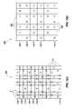
- the number of ground contacts across pixel array 500 including a plurality of pixels Pmay vary in a repeatable random pattern.
- rows 1 - 3 of pixel array 500may include a plurality of randomly distributed ground contacts (denoted by ‘X’).
- rows 4 - 6may include the same number of ground contacts, with the same positioning, as rows 1 - 3 .
- the examples described aboveare not intended to be limiting, and any even, calculated, or random distribution of the ground contacts across the pixel array 500 is within the scope of the embodiment of the invention.
- FIG. 7( b )illustrates a pixel structure array 500 ′ including a plurality of pixel structures, such as pixel structure 200 described above in reference to FIGS. 2 , 3 , and 4 .
- Ground contacts within the pixel structure array 500 ′may vary in a repeatable pattern throughout the array 500 ′.
- rows 1 and 2 of pixel structure array 500 ′may include a plurality of randomly distributed ground contacts (denoted by ‘X’). This two-row structure pattern may then be repeated for the remainder of the pixel structure array 500 ′.
- rows 3 and 4may include the same number of ground contacts, with the same positioning, as rows 1 and 2 .
- the examples described aboveare not intended to be limiting, and any even, calculated, or random distribution of the ground contacts within pixel structure array 500 ′ is within the scope of the embodiment of the invention.
- a processor-based system 600which includes an image sensor device 642 in accordance with an embodiment of the present invention is illustrated in FIG. 8 .
- a system 600may include a computer system, camera system scanner machine vision system, vehicle navigation system, video phone, surveillance system, auto focus system, star tracker system, motion detection system, image stabilization system, each of which may be configured to utilize an embodiment of the present invention.
- a processor-based system 600such as a computer system, for example, generally comprises a central processing unit (CPU) 644 , for example, a microprocessor that may communicate with an input/output (I/O) device 646 over a bus 652 .
- the image sensor device 642may also communicate with the system 600 over bus 652 .
- the system 600also includes random access memory (RAM) 648 , and, in the case of a computer system, may include peripheral devices such as a floppy disk drive 654 and a compact disk (CD) ROM drive 656 which also communicate with CPU 644 over bus 652 .
- Floppy disk drive 654 , image sensor device 642 and memory 648may be integrated on a single IC chip.
Landscapes
- Solid State Image Pick-Up Elements (AREA)
- Transforming Light Signals Into Electric Signals (AREA)
Abstract
Description
Claims (20)
Priority Applications (1)
| Application Number | Priority Date | Filing Date | Title |
|---|---|---|---|
| US12/271,577US7728279B2 (en) | 2007-03-06 | 2008-11-14 | Methods, devices, and systems related to pixel arrays |
Applications Claiming Priority (2)
| Application Number | Priority Date | Filing Date | Title |
|---|---|---|---|
| US11/714,561US7459668B2 (en) | 2007-03-06 | 2007-03-06 | Method, apparatus, and system to reduce ground resistance in a pixel array |
| US12/271,577US7728279B2 (en) | 2007-03-06 | 2008-11-14 | Methods, devices, and systems related to pixel arrays |
Related Parent Applications (1)
| Application Number | Title | Priority Date | Filing Date |
|---|---|---|---|
| US11/714,561ContinuationUS7459668B2 (en) | 2007-03-06 | 2007-03-06 | Method, apparatus, and system to reduce ground resistance in a pixel array |
Publications (2)
| Publication Number | Publication Date |
|---|---|
| US20090067702A1 US20090067702A1 (en) | 2009-03-12 |
| US7728279B2true US7728279B2 (en) | 2010-06-01 |
Family
ID=39509621
Family Applications (2)
| Application Number | Title | Priority Date | Filing Date |
|---|---|---|---|
| US11/714,561ActiveUS7459668B2 (en) | 2007-03-06 | 2007-03-06 | Method, apparatus, and system to reduce ground resistance in a pixel array |
| US12/271,577ActiveUS7728279B2 (en) | 2007-03-06 | 2008-11-14 | Methods, devices, and systems related to pixel arrays |
Family Applications Before (1)
| Application Number | Title | Priority Date | Filing Date |
|---|---|---|---|
| US11/714,561ActiveUS7459668B2 (en) | 2007-03-06 | 2007-03-06 | Method, apparatus, and system to reduce ground resistance in a pixel array |
Country Status (6)
| Country | Link |
|---|---|
| US (2) | US7459668B2 (en) |
| KR (1) | KR20090130286A (en) |
| CN (1) | CN101641789B (en) |
| GB (1) | GB2468375A (en) |
| TW (1) | TWI375322B (en) |
| WO (1) | WO2008109273A1 (en) |
Cited By (5)
| Publication number | Priority date | Publication date | Assignee | Title |
|---|---|---|---|---|
| US20110234873A1 (en)* | 2010-03-29 | 2011-09-29 | Sony Corporation | Solid-state image pickup element and image pickup apparatus |
| US20130021511A1 (en)* | 2008-11-28 | 2013-01-24 | Sony Corporation | Solid-state image pickup device, method for driving solid-state image pickup device, and image pickup apparatus |
| US8629926B2 (en) | 2011-11-04 | 2014-01-14 | Honeywell International, Inc. | Imaging apparatus comprising image sensor array having shared global shutter circuitry |
| US8749686B2 (en) | 2011-04-29 | 2014-06-10 | Truesense Imaging, Inc. | CCD image sensors and methods |
| US20210351213A1 (en)* | 2009-09-25 | 2021-11-11 | Sony Group Corporation | Solid-state imaging device and method for manufacturing solid-state imaging device, and electronic device |
Families Citing this family (21)
| Publication number | Priority date | Publication date | Assignee | Title |
|---|---|---|---|---|
| JP4599258B2 (en)* | 2005-09-16 | 2010-12-15 | 富士フイルム株式会社 | Solid-state image sensor |
| US7459668B2 (en)* | 2007-03-06 | 2008-12-02 | Micron Technology, Inc. | Method, apparatus, and system to reduce ground resistance in a pixel array |
| JP4350768B2 (en) | 2007-04-16 | 2009-10-21 | キヤノン株式会社 | Photoelectric conversion device and imaging device |
| KR20090125499A (en)* | 2008-06-02 | 2009-12-07 | 삼성전자주식회사 | CMOS image sensor and its driving method |
| EP2133918B1 (en)* | 2008-06-09 | 2015-01-28 | Sony Corporation | Solid-state imaging device, drive method thereof and electronic apparatus |
| JP5109962B2 (en)* | 2008-12-22 | 2012-12-26 | ソニー株式会社 | Solid-state imaging device and electronic apparatus |
| JP2010206172A (en)* | 2009-02-06 | 2010-09-16 | Canon Inc | Image sensing device, and camera |
| JP2010206174A (en) | 2009-02-06 | 2010-09-16 | Canon Inc | Photoelectric converter, method of manufacturing the same, and camera |
| JP2010206173A (en) | 2009-02-06 | 2010-09-16 | Canon Inc | Photoelectric conversion device and camera |
| JP5325006B2 (en)* | 2009-04-22 | 2013-10-23 | パナソニック株式会社 | Solid-state imaging device |
| US8193103B2 (en)* | 2010-07-29 | 2012-06-05 | Truesense Imaging, Inc. | CCD sensors with multiple contact patterns |
| US8742309B2 (en) | 2011-01-28 | 2014-06-03 | Aptina Imaging Corporation | Imagers with depth sensing capabilities |
| US10015471B2 (en) | 2011-08-12 | 2018-07-03 | Semiconductor Components Industries, Llc | Asymmetric angular response pixels for single sensor stereo |
| US8804021B2 (en)* | 2011-11-03 | 2014-08-12 | Omnivision Technologies, Inc. | Method, apparatus and system for providing improved full well capacity in an image sensor pixel |
| US9554115B2 (en)* | 2012-02-27 | 2017-01-24 | Semiconductor Components Industries, Llc | Imaging pixels with depth sensing capabilities |
| KR102383649B1 (en) | 2014-08-19 | 2022-04-08 | 삼성전자주식회사 | CMOS image sensor |
| US9900539B2 (en)* | 2015-09-10 | 2018-02-20 | Canon Kabushiki Kaisha | Solid-state image pickup element, and image pickup system |
| KR102473154B1 (en) | 2016-01-11 | 2022-12-02 | 에스케이하이닉스 주식회사 | Image sensor |
| CN106981495B (en)* | 2016-01-15 | 2019-10-25 | 中芯国际集成电路制造(上海)有限公司 | A kind of CMOS image sensor and its manufacturing method |
| TWI834644B (en)* | 2018-05-18 | 2024-03-11 | 日商索尼半導體解決方案公司 | Imaging components and electronic equipment |
| KR20230013704A (en) | 2021-07-19 | 2023-01-27 | 삼성전자주식회사 | Image sensor |
Citations (21)
| Publication number | Priority date | Publication date | Assignee | Title |
|---|---|---|---|---|
| US5877521A (en) | 1998-01-08 | 1999-03-02 | International Business Machines Corporation | SOI active pixel cell design with grounded body contact |
| US20010013577A1 (en) | 1999-12-31 | 2001-08-16 | Kyo-Seop Choo | X-ray image sensor and method for fabricating the same |
| US6326652B1 (en) | 1999-06-18 | 2001-12-04 | Micron Technology, Inc., | CMOS imager with a self-aligned buried contact |
| US20040262646A1 (en) | 2003-06-16 | 2004-12-30 | Inna Patrick | Pixel design to maximize photodiode capacitance and method of forming same |
| EP1530239A2 (en) | 2003-11-05 | 2005-05-11 | Sony Corporation | Solid-state imaging device |
| US6897082B2 (en) | 2003-06-16 | 2005-05-24 | Micron Technology, Inc. | Method of forming well for CMOS imager |
| US7002231B2 (en) | 2004-02-02 | 2006-02-21 | Micron Technology, Inc. | Barrier regions for image sensors |
| US20060043436A1 (en) | 2004-09-02 | 2006-03-02 | Micron Technology, Inc. | Contacts for CMOS imagers and method of formation |
| US20060044434A1 (en) | 2004-09-01 | 2006-03-02 | Canon Kabushiki Kaisha | Image pickup apparatus and image pickup system |
| US20060043437A1 (en) | 2004-08-24 | 2006-03-02 | Chandra Mouli | Transparent metal shielded isolation for image sensors |
| US20060043393A1 (en) | 2004-09-01 | 2006-03-02 | Canon Kabushiki Kaisha | Image pickup apparatus and image pickup system |
| US7037764B2 (en) | 2004-02-26 | 2006-05-02 | Micron Technology, Inc. | Method of forming a contact in a pixel cell |
| US20060175536A1 (en) | 2005-02-07 | 2006-08-10 | Samsung Electronics Co., Ltd. | CMOS sensor array with a shared structure |
| US20060175641A1 (en) | 2004-06-02 | 2006-08-10 | Micron Technology, Inc. | Raised photodiode sensor to increase fill factor and quantum efficiency in scaled pixels |
| US7091536B2 (en) | 2002-11-14 | 2006-08-15 | Micron Technology, Inc. | Isolation process and structure for CMOS imagers |
| US7091059B2 (en) | 2000-08-28 | 2006-08-15 | Micron Technology, Inc. | Method of forming a photosensor comprising a plurality of trenches |
| US7102180B2 (en) | 2002-11-26 | 2006-09-05 | Micron Technology, Inc. | CMOS imager pixel designs |
| US20060197169A1 (en) | 2005-03-07 | 2006-09-07 | Micron Technology, Inc. | Method and structure to reduce optical crosstalk in a solid state imager |
| US20060208285A1 (en) | 2005-03-17 | 2006-09-21 | Fujitsu Limited | Image sensor with embedded photodiode region and fabrication method thereof |
| US20060214201A1 (en) | 2003-06-16 | 2006-09-28 | Micron Technology, Inc. | Method and apparatus for reducing imager floating diffusion leakage |
| US7459668B2 (en)* | 2007-03-06 | 2008-12-02 | Micron Technology, Inc. | Method, apparatus, and system to reduce ground resistance in a pixel array |
Family Cites Families (1)
| Publication number | Priority date | Publication date | Assignee | Title |
|---|---|---|---|---|
| KR100669645B1 (en)* | 2002-11-12 | 2007-01-16 | 마이크론 테크놀로지, 인크 | Ground Gate and Isolation Technology to Reduce Dark Current in CMOS Image Sensors |
- 2007
- 2007-03-06USUS11/714,561patent/US7459668B2/enactiveActive
- 2008
- 2008-02-22KRKR1020097020882Apatent/KR20090130286A/ennot_activeCeased
- 2008-02-22WOPCT/US2008/054763patent/WO2008109273A1/enactiveApplication Filing
- 2008-02-22GBGB0915500Apatent/GB2468375A/ennot_activeWithdrawn
- 2008-02-22CNCN2008800072799Apatent/CN101641789B/ennot_activeExpired - Fee Related
- 2008-03-06TWTW097107923Apatent/TWI375322B/enactive
- 2008-11-14USUS12/271,577patent/US7728279B2/enactiveActive
Patent Citations (23)
| Publication number | Priority date | Publication date | Assignee | Title |
|---|---|---|---|---|
| US5877521A (en) | 1998-01-08 | 1999-03-02 | International Business Machines Corporation | SOI active pixel cell design with grounded body contact |
| US6326652B1 (en) | 1999-06-18 | 2001-12-04 | Micron Technology, Inc., | CMOS imager with a self-aligned buried contact |
| US20010013577A1 (en) | 1999-12-31 | 2001-08-16 | Kyo-Seop Choo | X-ray image sensor and method for fabricating the same |
| US6423973B2 (en) | 1999-12-31 | 2002-07-23 | Lg. Philips Lcd Co., Ltd. | X-ray image sensor and method for fabricating the same |
| US7091059B2 (en) | 2000-08-28 | 2006-08-15 | Micron Technology, Inc. | Method of forming a photosensor comprising a plurality of trenches |
| US7091536B2 (en) | 2002-11-14 | 2006-08-15 | Micron Technology, Inc. | Isolation process and structure for CMOS imagers |
| US7102180B2 (en) | 2002-11-26 | 2006-09-05 | Micron Technology, Inc. | CMOS imager pixel designs |
| US20060214201A1 (en) | 2003-06-16 | 2006-09-28 | Micron Technology, Inc. | Method and apparatus for reducing imager floating diffusion leakage |
| US6897082B2 (en) | 2003-06-16 | 2005-05-24 | Micron Technology, Inc. | Method of forming well for CMOS imager |
| US20040262646A1 (en) | 2003-06-16 | 2004-12-30 | Inna Patrick | Pixel design to maximize photodiode capacitance and method of forming same |
| US7009227B2 (en) | 2003-06-16 | 2006-03-07 | Micron Technology, Inc. | Photodiode structure and image pixel structure |
| EP1530239A2 (en) | 2003-11-05 | 2005-05-11 | Sony Corporation | Solid-state imaging device |
| US7002231B2 (en) | 2004-02-02 | 2006-02-21 | Micron Technology, Inc. | Barrier regions for image sensors |
| US7037764B2 (en) | 2004-02-26 | 2006-05-02 | Micron Technology, Inc. | Method of forming a contact in a pixel cell |
| US20060175641A1 (en) | 2004-06-02 | 2006-08-10 | Micron Technology, Inc. | Raised photodiode sensor to increase fill factor and quantum efficiency in scaled pixels |
| US20060043437A1 (en) | 2004-08-24 | 2006-03-02 | Chandra Mouli | Transparent metal shielded isolation for image sensors |
| US20060043393A1 (en) | 2004-09-01 | 2006-03-02 | Canon Kabushiki Kaisha | Image pickup apparatus and image pickup system |
| US20060044434A1 (en) | 2004-09-01 | 2006-03-02 | Canon Kabushiki Kaisha | Image pickup apparatus and image pickup system |
| US20060043436A1 (en) | 2004-09-02 | 2006-03-02 | Micron Technology, Inc. | Contacts for CMOS imagers and method of formation |
| US20060175536A1 (en) | 2005-02-07 | 2006-08-10 | Samsung Electronics Co., Ltd. | CMOS sensor array with a shared structure |
| US20060197169A1 (en) | 2005-03-07 | 2006-09-07 | Micron Technology, Inc. | Method and structure to reduce optical crosstalk in a solid state imager |
| US20060208285A1 (en) | 2005-03-17 | 2006-09-21 | Fujitsu Limited | Image sensor with embedded photodiode region and fabrication method thereof |
| US7459668B2 (en)* | 2007-03-06 | 2008-12-02 | Micron Technology, Inc. | Method, apparatus, and system to reduce ground resistance in a pixel array |
Non-Patent Citations (1)
| Title |
|---|
| International Search Report dated Jul. 7, 2008, for International Application No. PCT/US2008/054763 (5 pages). |
Cited By (14)
| Publication number | Priority date | Publication date | Assignee | Title |
|---|---|---|---|---|
| US9077920B2 (en)* | 2008-11-28 | 2015-07-07 | Sony Corporation | Solid-state image pickup device, method for driving solid-state image pickup device, and image pickup apparatus |
| US20130021511A1 (en)* | 2008-11-28 | 2013-01-24 | Sony Corporation | Solid-state image pickup device, method for driving solid-state image pickup device, and image pickup apparatus |
| US12310130B2 (en)* | 2009-09-25 | 2025-05-20 | Sony Group Corporation | Solid-state imaging device and method for manufacturing solid-state imaging device, and electronic device |
| US20210351213A1 (en)* | 2009-09-25 | 2021-11-11 | Sony Group Corporation | Solid-state imaging device and method for manufacturing solid-state imaging device, and electronic device |
| US9406707B2 (en) | 2010-03-29 | 2016-08-02 | Sony Corporation | Solid-state image pickup element and image pickup apparatus |
| US8780247B2 (en)* | 2010-03-29 | 2014-07-15 | Sony Corporation | Solid-state image pickup element and image pickup apparatus |
| US9236508B2 (en) | 2010-03-29 | 2016-01-12 | Sony Corporation | Solid-state image pickup element and image pickup apparatus |
| US20110234873A1 (en)* | 2010-03-29 | 2011-09-29 | Sony Corporation | Solid-state image pickup element and image pickup apparatus |
| US9728576B2 (en) | 2010-03-29 | 2017-08-08 | Sony Corporation | Solid-state image pickup element and image pickup apparatus |
| US10224362B2 (en) | 2010-03-29 | 2019-03-05 | Sony Corporation | Solid-state image pickup element and image pickup apparatus |
| US8749686B2 (en) | 2011-04-29 | 2014-06-10 | Truesense Imaging, Inc. | CCD image sensors and methods |
| US9066032B2 (en) | 2011-11-04 | 2015-06-23 | Honeywell International Inc. | Imaging apparatus comprising image sensor array having shared global shutter circuitry |
| US9407840B2 (en) | 2011-11-04 | 2016-08-02 | Honeywell International, Inc. | Imaging apparatus comprising image sensor array having shared global shutter circuitry |
| US8629926B2 (en) | 2011-11-04 | 2014-01-14 | Honeywell International, Inc. | Imaging apparatus comprising image sensor array having shared global shutter circuitry |
Also Published As
| Publication number | Publication date |
|---|---|
| GB0915500D0 (en) | 2009-10-07 |
| US20090067702A1 (en) | 2009-03-12 |
| WO2008109273A1 (en) | 2008-09-12 |
| TW200901454A (en) | 2009-01-01 |
| US7459668B2 (en) | 2008-12-02 |
| CN101641789A (en) | 2010-02-03 |
| WO2008109273B1 (en) | 2008-10-30 |
| GB2468375A (en) | 2010-09-08 |
| KR20090130286A (en) | 2009-12-22 |
| CN101641789B (en) | 2012-02-22 |
| TWI375322B (en) | 2012-10-21 |
| US20080217718A1 (en) | 2008-09-11 |
Similar Documents
| Publication | Publication Date | Title |
|---|---|---|
| US7728279B2 (en) | Methods, devices, and systems related to pixel arrays | |
| US12068352B2 (en) | Solid-state imaging device, with transfer transistor gate electrode having trench gate sections | |
| US11798962B2 (en) | Solid-state imaging device with a pixel having a partially shielded photoelectric conversion unit region for holding charge | |
| US7671314B2 (en) | Image sensor including active pixel sensor array with photoelectric conversion region | |
| US10536652B2 (en) | Image sensors with split photodiodes | |
| US7541628B2 (en) | Image sensors including active pixel sensor arrays | |
| US7880255B2 (en) | Pixel cell having a grated interface | |
| KR100971082B1 (en) | Solid Imager with Capacitor on Red Pixel | |
| US8411174B2 (en) | Shielding black reference pixels in image sensors | |
| JP5326507B2 (en) | Solid-state imaging device, driving method of solid-state imaging device, and electronic apparatus | |
| US8339494B1 (en) | Image sensor with controllable vertically integrated photodetectors | |
| KR20230025932A (en) | Solid state imaging device and manufacturing method therefor, and electronic apparatus | |
| JP2009505437A (en) | Method and apparatus for protecting correction pixels from false charges in an imager | |
| US8730362B2 (en) | Image sensor with controllable vertically integrated photodetectors | |
| US8829637B2 (en) | Image sensor with controllable vertically integrated photodetectors using a buried layer | |
| US8946612B2 (en) | Image sensor with controllable vertically integrated photodetectors | |
| US8736728B2 (en) | Image sensor with controllable vertically integrated photodetectors | |
| US20050168604A1 (en) | Solid-state image pickup device and module type solid-state image pickup device | |
| US20090302323A1 (en) | Method and apparatus for providing a low-level interconnect section in an imager device |
Legal Events
| Date | Code | Title | Description |
|---|---|---|---|
| AS | Assignment | Owner name:APTINA IMAGING CORPORATION, CAYMAN ISLANDS Free format text:ASSIGNMENT OF ASSIGNORS INTEREST;ASSIGNOR:MICRON TECHNOLOGY, INC.;REEL/FRAME:022822/0116 Effective date:20080926 Owner name:APTINA IMAGING CORPORATION, CAYMAN ISLANDS Free format text:ASSIGNMENT OF ASSIGNORS INTEREST;ASSIGNOR:MICRON TECHNOLOGY, INC.;REEL/FRAME:022822/0130 Effective date:20080926 Owner name:APTINA IMAGING CORPORATION,CAYMAN ISLANDS Free format text:ASSIGNMENT OF ASSIGNORS INTEREST;ASSIGNOR:MICRON TECHNOLOGY, INC.;REEL/FRAME:022822/0116 Effective date:20080926 Owner name:APTINA IMAGING CORPORATION,CAYMAN ISLANDS Free format text:ASSIGNMENT OF ASSIGNORS INTEREST;ASSIGNOR:MICRON TECHNOLOGY, INC.;REEL/FRAME:022822/0130 Effective date:20080926 | |
| STCF | Information on status: patent grant | Free format text:PATENTED CASE | |
| FPAY | Fee payment | Year of fee payment:4 | |
| AS | Assignment | Owner name:MICRON TECHNOLOGY, INC., IDAHO Free format text:ASSIGNMENT OF ASSIGNORS INTEREST;ASSIGNOR:MAURITZSON, RICHARD A.;REEL/FRAME:040482/0909 Effective date:20070302 | |
| MAFP | Maintenance fee payment | Free format text:PAYMENT OF MAINTENANCE FEE, 8TH YEAR, LARGE ENTITY (ORIGINAL EVENT CODE: M1552) Year of fee payment:8 | |
| MAFP | Maintenance fee payment | Free format text:PAYMENT OF MAINTENANCE FEE, 12TH YEAR, LARGE ENTITY (ORIGINAL EVENT CODE: M1553); ENTITY STATUS OF PATENT OWNER: LARGE ENTITY Year of fee payment:12 |