US7727875B2 - Grooving bumped wafer pre-underfill system - Google Patents
Grooving bumped wafer pre-underfill systemDownload PDFInfo
- Publication number
- US7727875B2 US7727875B2US11/766,710US76671007AUS7727875B2US 7727875 B2US7727875 B2US 7727875B2US 76671007 AUS76671007 AUS 76671007AUS 7727875 B2US7727875 B2US 7727875B2
- Authority
- US
- United States
- Prior art keywords
- adhesive layer
- bumped wafer
- wafer
- coating
- layer
- Prior art date
- Legal status (The legal status is an assumption and is not a legal conclusion. Google has not performed a legal analysis and makes no representation as to the accuracy of the status listed.)
- Active, expires
Links
- 238000000034methodMethods0.000claimsabstractdescription140
- 239000012790adhesive layerSubstances0.000claimsabstractdescription99
- 239000010410layerSubstances0.000claimsabstractdescription64
- 239000004065semiconductorSubstances0.000claimsabstractdescription29
- 238000005520cutting processMethods0.000claimsabstractdescription9
- 230000008569processEffects0.000claimsdescription69
- 239000000463materialSubstances0.000claimsdescription62
- 239000011248coating agentSubstances0.000claimsdescription39
- 238000000576coating methodMethods0.000claimsdescription39
- 229910000679solderInorganic materials0.000claimsdescription16
- 238000004519manufacturing processMethods0.000claimsdescription11
- 238000000227grindingMethods0.000claimsdescription8
- 238000003475laminationMethods0.000claimsdescription8
- 238000007650screen-printingMethods0.000claimsdescription8
- 238000004528spin coatingMethods0.000claimsdescription8
- 229920005992thermoplastic resinPolymers0.000claimsdescription8
- 239000004642PolyimideSubstances0.000claimsdescription6
- 229920001721polyimidePolymers0.000claimsdescription6
- 238000010030laminatingMethods0.000claimsdescription4
- 230000001070adhesive effectEffects0.000description14
- 239000000853adhesiveSubstances0.000description12
- 238000005336crackingMethods0.000description8
- 239000004020conductorSubstances0.000description6
- 238000000151depositionMethods0.000description6
- 230000008901benefitEffects0.000description5
- 230000008021depositionEffects0.000description5
- 239000000758substrateSubstances0.000description5
- 239000010949copperSubstances0.000description4
- 230000007812deficiencyEffects0.000description4
- 239000010931goldSubstances0.000description4
- 239000011368organic materialSubstances0.000description3
- 239000002861polymer materialSubstances0.000description3
- 239000011800void materialSubstances0.000description3
- RYGMFSIKBFXOCR-UHFFFAOYSA-NCopperChemical compound[Cu]RYGMFSIKBFXOCR-UHFFFAOYSA-N0.000description2
- 239000004593EpoxySubstances0.000description2
- -1acrylChemical group0.000description2
- 239000002390adhesive tapeSubstances0.000description2
- 238000013459approachMethods0.000description2
- 229910052802copperInorganic materials0.000description2
- 229910003460diamondInorganic materials0.000description2
- 239000010432diamondSubstances0.000description2
- 230000000694effectsEffects0.000description2
- PCHJSUWPFVWCPO-UHFFFAOYSA-NgoldChemical compound[Au]PCHJSUWPFVWCPO-UHFFFAOYSA-N0.000description2
- 229910052737goldInorganic materials0.000description2
- 238000012986modificationMethods0.000description2
- 230000004048modificationEffects0.000description2
- 229920000642polymerPolymers0.000description2
- 238000003825pressingMethods0.000description2
- 238000005476solderingMethods0.000description2
- XUIMIQQOPSSXEZ-UHFFFAOYSA-NSiliconChemical compound[Si]XUIMIQQOPSSXEZ-UHFFFAOYSA-N0.000description1
- 230000006978adaptationEffects0.000description1
- 230000002411adverseEffects0.000description1
- 230000001413cellular effectEffects0.000description1
- 239000000919ceramicSubstances0.000description1
- 238000007796conventional methodMethods0.000description1
- 238000004070electrodepositionMethods0.000description1
- 230000001747exhibiting effectEffects0.000description1
- 238000010438heat treatmentMethods0.000description1
- 238000002844meltingMethods0.000description1
- 230000008018meltingEffects0.000description1
- 238000004806packaging method and processMethods0.000description1
- 238000012545processingMethods0.000description1
- 239000011253protective coatingSubstances0.000description1
- 230000001681protective effectEffects0.000description1
- 230000009467reductionEffects0.000description1
- 238000003303reheatingMethods0.000description1
- 229910052710siliconInorganic materials0.000description1
- 239000010703siliconSubstances0.000description1
- 229940095676wafer productDrugs0.000description1
Images


Classifications
- H—ELECTRICITY
- H01—ELECTRIC ELEMENTS
- H01L—SEMICONDUCTOR DEVICES NOT COVERED BY CLASS H10
- H01L21/00—Processes or apparatus adapted for the manufacture or treatment of semiconductor or solid state devices or of parts thereof
- H01L21/70—Manufacture or treatment of devices consisting of a plurality of solid state components formed in or on a common substrate or of parts thereof; Manufacture of integrated circuit devices or of parts thereof
- H01L21/77—Manufacture or treatment of devices consisting of a plurality of solid state components or integrated circuits formed in, or on, a common substrate
- H01L21/78—Manufacture or treatment of devices consisting of a plurality of solid state components or integrated circuits formed in, or on, a common substrate with subsequent division of the substrate into plural individual devices
- H—ELECTRICITY
- H01—ELECTRIC ELEMENTS
- H01L—SEMICONDUCTOR DEVICES NOT COVERED BY CLASS H10
- H01L21/00—Processes or apparatus adapted for the manufacture or treatment of semiconductor or solid state devices or of parts thereof
- H01L21/02—Manufacture or treatment of semiconductor devices or of parts thereof
- H01L21/04—Manufacture or treatment of semiconductor devices or of parts thereof the devices having potential barriers, e.g. a PN junction, depletion layer or carrier concentration layer
- H01L21/50—Assembly of semiconductor devices using processes or apparatus not provided for in a single one of the groups H01L21/18 - H01L21/326 or H10D48/04 - H10D48/07 e.g. sealing of a cap to a base of a container
- H01L21/56—Encapsulations, e.g. encapsulation layers, coatings
- H01L21/561—Batch processing
- H—ELECTRICITY
- H01—ELECTRIC ELEMENTS
- H01L—SEMICONDUCTOR DEVICES NOT COVERED BY CLASS H10
- H01L21/00—Processes or apparatus adapted for the manufacture or treatment of semiconductor or solid state devices or of parts thereof
- H01L21/02—Manufacture or treatment of semiconductor devices or of parts thereof
- H01L21/04—Manufacture or treatment of semiconductor devices or of parts thereof the devices having potential barriers, e.g. a PN junction, depletion layer or carrier concentration layer
- H01L21/50—Assembly of semiconductor devices using processes or apparatus not provided for in a single one of the groups H01L21/18 - H01L21/326 or H10D48/04 - H10D48/07 e.g. sealing of a cap to a base of a container
- H01L21/56—Encapsulations, e.g. encapsulation layers, coatings
- H01L21/568—Temporary substrate used as encapsulation process aid
- H—ELECTRICITY
- H01—ELECTRIC ELEMENTS
- H01L—SEMICONDUCTOR DEVICES NOT COVERED BY CLASS H10
- H01L21/00—Processes or apparatus adapted for the manufacture or treatment of semiconductor or solid state devices or of parts thereof
- H01L21/67—Apparatus specially adapted for handling semiconductor or electric solid state devices during manufacture or treatment thereof; Apparatus specially adapted for handling wafers during manufacture or treatment of semiconductor or electric solid state devices or components ; Apparatus not specifically provided for elsewhere
- H01L21/683—Apparatus specially adapted for handling semiconductor or electric solid state devices during manufacture or treatment thereof; Apparatus specially adapted for handling wafers during manufacture or treatment of semiconductor or electric solid state devices or components ; Apparatus not specifically provided for elsewhere for supporting or gripping
- H01L21/6835—Apparatus specially adapted for handling semiconductor or electric solid state devices during manufacture or treatment thereof; Apparatus specially adapted for handling wafers during manufacture or treatment of semiconductor or electric solid state devices or components ; Apparatus not specifically provided for elsewhere for supporting or gripping using temporarily an auxiliary support
- H01L21/6836—Wafer tapes, e.g. grinding or dicing support tapes
- H—ELECTRICITY
- H01—ELECTRIC ELEMENTS
- H01L—SEMICONDUCTOR DEVICES NOT COVERED BY CLASS H10
- H01L2224/00—Indexing scheme for arrangements for connecting or disconnecting semiconductor or solid-state bodies and methods related thereto as covered by H01L24/00
- H01L2224/01—Means for bonding being attached to, or being formed on, the surface to be connected, e.g. chip-to-package, die-attach, "first-level" interconnects; Manufacturing methods related thereto
- H01L2224/10—Bump connectors; Manufacturing methods related thereto
- H01L2224/15—Structure, shape, material or disposition of the bump connectors after the connecting process
- H01L2224/16—Structure, shape, material or disposition of the bump connectors after the connecting process of an individual bump connector
- H—ELECTRICITY
- H01—ELECTRIC ELEMENTS
- H01L—SEMICONDUCTOR DEVICES NOT COVERED BY CLASS H10
- H01L2224/00—Indexing scheme for arrangements for connecting or disconnecting semiconductor or solid-state bodies and methods related thereto as covered by H01L24/00
- H01L2224/01—Means for bonding being attached to, or being formed on, the surface to be connected, e.g. chip-to-package, die-attach, "first-level" interconnects; Manufacturing methods related thereto
- H01L2224/26—Layer connectors, e.g. plate connectors, solder or adhesive layers; Manufacturing methods related thereto
- H01L2224/27—Manufacturing methods
- H01L2224/274—Manufacturing methods by blanket deposition of the material of the layer connector
- H01L2224/2741—Manufacturing methods by blanket deposition of the material of the layer connector in liquid form
- H01L2224/27416—Spin coating
- H—ELECTRICITY
- H01—ELECTRIC ELEMENTS
- H01L—SEMICONDUCTOR DEVICES NOT COVERED BY CLASS H10
- H01L2224/00—Indexing scheme for arrangements for connecting or disconnecting semiconductor or solid-state bodies and methods related thereto as covered by H01L24/00
- H01L2224/73—Means for bonding being of different types provided for in two or more of groups H01L2224/10, H01L2224/18, H01L2224/26, H01L2224/34, H01L2224/42, H01L2224/50, H01L2224/63, H01L2224/71
- H01L2224/731—Location prior to the connecting process
- H01L2224/73101—Location prior to the connecting process on the same surface
- H01L2224/73103—Bump and layer connectors
- H01L2224/73104—Bump and layer connectors the bump connector being embedded into the layer connector
- H—ELECTRICITY
- H01—ELECTRIC ELEMENTS
- H01L—SEMICONDUCTOR DEVICES NOT COVERED BY CLASS H10
- H01L23/00—Details of semiconductor or other solid state devices
- H01L23/28—Encapsulations, e.g. encapsulating layers, coatings, e.g. for protection
- H01L23/31—Encapsulations, e.g. encapsulating layers, coatings, e.g. for protection characterised by the arrangement or shape
- H01L23/3107—Encapsulations, e.g. encapsulating layers, coatings, e.g. for protection characterised by the arrangement or shape the device being completely enclosed
- H01L23/3114—Encapsulations, e.g. encapsulating layers, coatings, e.g. for protection characterised by the arrangement or shape the device being completely enclosed the device being a chip scale package, e.g. CSP
- H—ELECTRICITY
- H01—ELECTRIC ELEMENTS
- H01L—SEMICONDUCTOR DEVICES NOT COVERED BY CLASS H10
- H01L24/00—Arrangements for connecting or disconnecting semiconductor or solid-state bodies; Methods or apparatus related thereto
- H01L24/01—Means for bonding being attached to, or being formed on, the surface to be connected, e.g. chip-to-package, die-attach, "first-level" interconnects; Manufacturing methods related thereto
- H01L24/10—Bump connectors ; Manufacturing methods related thereto
- H01L24/12—Structure, shape, material or disposition of the bump connectors prior to the connecting process
- H01L24/13—Structure, shape, material or disposition of the bump connectors prior to the connecting process of an individual bump connector
- H—ELECTRICITY
- H01—ELECTRIC ELEMENTS
- H01L—SEMICONDUCTOR DEVICES NOT COVERED BY CLASS H10
- H01L2924/00—Indexing scheme for arrangements or methods for connecting or disconnecting semiconductor or solid-state bodies as covered by H01L24/00
- H01L2924/0001—Technical content checked by a classifier
- H01L2924/00011—Not relevant to the scope of the group, the symbol of which is combined with the symbol of this group
- H—ELECTRICITY
- H01—ELECTRIC ELEMENTS
- H01L—SEMICONDUCTOR DEVICES NOT COVERED BY CLASS H10
- H01L2924/00—Indexing scheme for arrangements or methods for connecting or disconnecting semiconductor or solid-state bodies as covered by H01L24/00
- H01L2924/0001—Technical content checked by a classifier
- H01L2924/00014—Technical content checked by a classifier the subject-matter covered by the group, the symbol of which is combined with the symbol of this group, being disclosed without further technical details
- H—ELECTRICITY
- H01—ELECTRIC ELEMENTS
- H01L—SEMICONDUCTOR DEVICES NOT COVERED BY CLASS H10
- H01L2924/00—Indexing scheme for arrangements or methods for connecting or disconnecting semiconductor or solid-state bodies as covered by H01L24/00
- H01L2924/01—Chemical elements
- H01L2924/01079—Gold [Au]
- H—ELECTRICITY
- H01—ELECTRIC ELEMENTS
- H01L—SEMICONDUCTOR DEVICES NOT COVERED BY CLASS H10
- H01L2924/00—Indexing scheme for arrangements or methods for connecting or disconnecting semiconductor or solid-state bodies as covered by H01L24/00
- H01L2924/10—Details of semiconductor or other solid state devices to be connected
- H01L2924/11—Device type
- H01L2924/14—Integrated circuits
Definitions
- the present inventionrelates in general to electronic devices and, more particularly, to a method of forming a semiconductor device utilizing a pre-underfill material disposed over a bumped wafer structure.
- Semiconductorsor computer chips, are found in virtually every electrical product manufactured today. Semiconductors are used not only in sophisticated industrial and commercial electronic equipment, but also in many household and consumer items such as televisions, clothes washers and dryers, radios, and telephones. As products become smaller but more functional, there is a need to include more semiconductors in the smaller products to perform the functionality. The reduction in size of cellular telephones is one example of how more capabilities are incorporated into smaller electronic products.
- a so-called “flip chip”is generally a monolithic semiconductor device, such as an integrated circuit, having bead-like terminals formed on one surface of the chip.
- the terminalsserve to both secure the chip to a circuit board and electrically connect the flip chip's circuitry to a conductor pattern formed on the circuit board, which may be a ceramic substrate, printed wiring board, flexible circuit, or a silicon substrate. Due to the numerous functions typically performed by the micro-circuitry of a flip chip, a relatively large number of terminals are required.
- soldering a flip chip to its conductor patternrequires a high degree of precision.
- Reflow solder techniquesare widely utilized in the soldering of flip chips. Such techniques typically involve forming solder bumps on the surface of the flip chip using methods such as electrodeposition, by which a quantity of solder is accurately deposited on one surface of the flip chip. Heating the solder above its melting temperature serves to form the characteristic solder bumps. The chip is then soldered to the conductor pattern by registering the solder bumps with their respective conductors, and reheating, or reflowing, the solder so as to metallurgically and electrically bond the chip to the conductor pattern.
- underfill materialIn flip chip packaging and other semiconductor devices, a so-called “underfill” material is provided between the substrate and the die to promote device reliability characteristics.
- Various methodsare known in the art for depositing the underfill material, including deposition through an opening of the substrate so as to fill in a gap between the substrate and the die. More recently, techniques involving the application of a film to a bumped wafer have been utilized.
- the present inventionis a method of forming a semiconductor device comprising providing a bumped wafer, forming a plurality of grooves in an active surface of the bumped wafer, disposing a pre-underfill layer over the active surface, filling the plurality of grooves, mounting a first adhesive layer to the pre-underfill layer, and grinding a back surface of the bumped wafer, mounting a second adhesive layer to the back surface of the bumped wafer and peeling off the first adhesive layer from the active surface of the bumped wafer, or mounting the second adhesive layer to the first adhesive layer, and singulating the bumped wafer into a plurality of segments by cutting the bumped wafer along the plurality of grooves.
- the present inventionis a method of forming a semiconductor device comprising providing a bumped wafer, forming a plurality of grooves in an active surface of the bumped wafer, disposing a pre-underfill layer over the active surface, filling the plurality of grooves, laminating a first adhesive layer to the pre-underfill layer, and grinding a back surface of the bumped wafer, disposing a coating over the back surface of the bumped wafer, mounting a second adhesive layer to the coating and peeling off the first adhesive layer from the active surface of the bumped wafer, or mounting the second adhesive layer to the first adhesive layer, and singulating the bumped wafer into a plurality of segments by cutting the bumped wafer along the plurality of grooves.
- the present inventionis a method of manufacturing a semiconductor device comprising providing a bumped wafer having a plurality of grooves formed in an active surface of the bumped wafer, providing a pre-underfill layer disposed over the active surface, filling the plurality of grooves, providing a first adhesive layer mounted to the pre-underfill layer, and providing a second adhesive layer mounted to a back surface of the bumped wafer, or mounted to the first adhesive layer.
- the present inventionis a method of manufacturing a semiconductor device comprising providing a bumped wafer having a plurality of grooves formed in an active surface of the bumped wafer, providing a pre-underfill layer disposed over the active surface, filling the plurality of grooves, providing a coating disposed over a back surface of the bumped wafer, providing a first adhesive layer mounted to the pre-underfill layer, and providing a second adhesive layer mounted to the coating, or mounted to the first adhesive layer.
- FIG. 1illustrates an exemplary prior art semiconductor wafer having a bottom surface protective coating
- FIG. 2illustrates an exemplary prior art sheet forming a protective film for semiconductor chips
- FIG. 3illustrates a first step in a first exemplary method of forming a semiconductor device using a grooved bumped wafer structure and a pre-underfill material, showing a grooved bumped wafer structure;
- FIG. 4illustrates a second step in the first exemplary method begun with FIG. 3 , of forming a semiconductor device using a grooved bumped wafer structure and a pre-underfill material, showing the deposition of the pre-underfill material over the bumped wafer;
- FIG. 5illustrates a third step in the first exemplary method begun with FIG. 3 , of forming a semiconductor device using a grooved bumped wafer structure and a pre-underfill material, showing the application of a first adhesive layer;
- FIG. 6Aillustrates a first option of a fourth step in the first exemplary method begun with FIG. 3 , where a second adhesive layer is connected to the first adhesive layer;
- FIG. 6Billustrates a second option of the fourth step in the first exemplary method begun with FIG. 3 , where the second adhesive layer is connected to a back surface of the bumped wafer;
- FIGS. 7A and 7Billustrate first and second options of a fifth step in the first exemplary method begun with FIG. 3 , respectively, where the bumped wafer is singulated into a plurality of segments;
- FIG. 8Aillustrates a first option of a sixth step in the first exemplary method begun with FIG. 3 , where a die attach process removes a bump from the bumped wafer segment;
- FIG. 8Billustrates a second option of the sixth step in the first exemplary method begun with FIG. 3 , where a chip attach process removes the bumped wafer segment from the second adhesive layer;
- FIG. 9illustrates a first step in a second exemplary method of forming a semiconductor device using a grooved bumped wafer structure and a pre-underfill material, showing a grooved bumped wafer structure
- FIG. 10illustrates a second step in the second exemplary method begun with FIG. 9 , of forming a semiconductor device using a grooved bumped wafer structure and a pre-underfill material, showing the deposition of the pre-underfill material over the bumped wafer structure;
- FIG. 11illustrates a third step in the second exemplary method begun with FIG. 3 , of forming a semiconductor device using a grooved bumped wafer structure and a pre-underfill material, where a first adhesive layer is connected to an active surface of the bumped wafer;
- FIG. 12illustrates a fourth step in the second exemplary method begun with FIG. 9 , where a coating is disposed over the back surface of the bumped wafer;
- FIG. 13Aillustrates a first option of a fifth step in the second exemplary method begun with FIG. 9 , where a second adhesive layer is connected to the first adhesive layer;
- FIG. 13Billustrates a second option of the fifth step in the second exemplary method begun with FIG. 9 , where the second adhesive layer is connected to the coating;
- FIGS. 14A and 14Billustrate first and second options of a sixth step in the second exemplary method begun with FIG. 9 , respectively, where the bumped wafer is singulated into a plurality of segments;
- FIG. 15Aillustrates a first option of a seventh step in the second exemplary method begun with FIG. 9 , where a die attach process removes a bump from the bumped wafer segment;
- FIG. 15Billustrates a second option of the sixth step in the second exemplary method begun with FIG. 9 , where a chip attach process removes the bumped wafer segment from the second adhesive layer;
- FIG. 16Aconceptually illustrates a bumped wafer structure having backside chipping deficiencies
- FIG. 16Bconceptually illustrates a bumped wafer structure having markedly less backside chipping deficiencies
- FIG. 17Aillustrates an exemplary prior art drawback resulting from peeling of conventional underfill layer
- FIG. 17Bconceptually illustrates benefits associated with a pre-underfill material upon removal of a conventional adhesive layer
- FIG. 18conceptually illustrates benefits associated with thinner bumped wafer structures
- FIG. 19Aillustrates a first step in a first exemplary method for a die attachment process
- FIG. 19Billustrates a second step in a die attachment process
- FIG. 20Aillustrates a first step in a chip attachment process
- FIG. 20Billustrates a second step in a chip attachment process
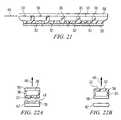
- FIG. 21conceptually illustrates the application of a coating over a backside of a bumped wafer structure
- FIG. 22Aillustrates a die attachment process performed incorporating a backside coating
- FIG. 22Billustrates a chip attachment process performed incorporating a backside coating.
- FIG. 1illustrates an exemplary prior art semiconductor flip chip device 10 , having a die 12 with a bottom surface 14 and a top surface 16 .
- a dicing saw tape 18is adhered directly to bottom surface 14 as shown.
- a plurality of bumps 20are formed on the top surface 16 of die 12 .
- Dicing saw tape 18is intended to prevent chipping during a dicing process undergone by flip chip device 10 .
- FIG. 2illustrates a second exemplary prior art semiconductor device 22 including a bumped semiconductor wafer 24 , a release layer 26 , and a base film 28 .
- Base film 28is intended to eliminate adverse effects of mechanical grinding on the back surface of wafer 24 , as well as to reduce chipping during subsequent dicing processes.
- the present inventionimproves upon the techniques described in the prior art to enable the use of a thin, bumped wafer structure (e.g., less than 100 um thickness) without chipping or cracking during a subsequent dicing process, die attach process, and chip attach process.
- a thin, bumped wafer structuree.g., less than 100 um thickness
- a bumped wafer 30has a plurality of bumps 32 .
- the bumps 32represent solder bumps, gold (Au) bumps, or copper (Cu) bumps.
- the bumped wafer 30undergoes a dicing process to form a plurality of grooves 34 in the active surface of wafer 30 as depicted.
- the dicing processuses a diamond blade or laser.
- FIG. 4depicts a second step in the first exemplary method begun with FIG. 3 .
- a wafer-level pre-underfill material 36is deposited over the active surface of wafer 30 as shown.
- the material 36can include polyimide (Pi), thermoplastic resin, similar polymer and/or organic materials.
- Pre-underfill layer 36can also include an epoxy or acryl materials having adhesive characteristics.
- the material 36can be deposited by spin-coating or screen printing methods. As seen, the material 36 provides an even coating over wafer 30 . Each of the grooves 34 formed in the surface of wafer 30 is filled by pre-underfill material 36 .
- FIG. 5illustrates a third step in the first exemplary method begun with FIG. 3 .
- a first adhesive material layer 38is disposed on pre-underfill layer 36 as shown.
- the adhesive material 38can include an adhesive, such as lamination tape.
- the adhesive layer 38can include such materials as ultraviolet (UV) tape, thermoplastic resin, photo-resist, or other materials that have adhesive properties. In many cases, UV tape can be implemented to impart peeling convenience.
- the layer 38can also be applied by a pressing operation.
- the wafer 30is inverted and a backgrinding process using a grinding wheel is performed to the back surface 40 to reduce the thickness of wafer 30 .
- wafer 30is protected from chipping and cracking during a subsequent die attach or chip attach process.
- the adhesive material 38 attached to the pre-underfill material 36provides structural support to wafer 30 during the backgrinding operation, which can result in a thinner wafer having less warping and other physical deficiencies.
- FIG. 6Aillustrates a first option for a fourth step in the exemplary method begun with FIG. 3 .
- the first optioninvolves applying a second adhesive layer 42 to the first adhesive layer 38 .
- the second adhesive layer 42can also include various adhesive materials such as lamination tape.
- FIG. 6Billustrates the second adhesive layer 42 applied to the back surface of wafer 30 .
- the first adhesive layer 38is removed from the pre-underfill layer 36 as shown.
- the layer 38can be removed using a peeling process.
- the wafer 30can be inverted prior to the removal step, as shown.
- a portion of bumps 32are exposed following the removal of layer 38 .
- FIGS. 7A and 7Bcollectively illustrate the next, fifth step in the exemplary method begun with FIG. 3 , for the case where adhesive layer 42 is mounted to adhesive layer 38 , and for the case where adhesive layer 42 is mounted directly to wafer 30 , respectively.
- FIG. 7Aillustrates the dicing saw process of forming saw cuts 44 to correspond with each of the filled grooves 34 of bumped wafer 30 .
- the cuts 44can be formed with a dicing saw, or with similar manufacturing tool. As shown in FIG. 7A , the cuts extend to a portion of adhesive layer 38 .
- Layer 42is left uncut so as to collectively retain individual cut segments of wafer 30 and to continue to provide structural support as the segments of wafer 30 are moved.
- FIG. 7Billustrates the sawing process for the case where adhesive layer 42 is applied directly to the back side of wafer 30 .
- Cuts 44are oriented to correspond with each of the plurality of filled grooves 34 of the bumped wafer 30 .
- the cuts 44extend into a portion of the layer 42 , but do not cut through the layer 42 entirely.
- layer 42continues to provide structural support and collectively holds the segments of wafer 30 in place.
- FIG. 8Aa die attach process is shown in the case where layers 38 and 42 are directly attached.
- the die attach processcan proceed using tools and processes known in the art.
- An individual segment of the plurality of segments of wafer 30are shown for conceptual purposes of illustration.
- the segment 30is lifted as denoted by arrow 46 from adhesive layers 38 and 42 .
- the bumps 32are protected by layers 38 and 42 prior to the die attach process, which leaves behind void 48 in layer 38 .
- FIG. 8Ba chip attach process is shown which again lifts a segment of the bumped wafer 30 , as denoted by arrow 46 , to separate the segment from adhesive layer 42 .
- the bumped wafer 30has a plurality of bumps 32 .
- the bumps 32represent solder bumps, gold (Au) bumps, or copper (Cu) bumps.
- the bumped wafer 30undergoes a dicing process to form a plurality of grooves 34 in the active surface of wafer 30 as depicted.
- FIG. 10depicts a second step in the second exemplary method begun with FIG. 9 .
- a wafer-level pre-underfill material 36is deposited over the active surface of wafer 30 as shown.
- the material 36can include polyimide (Pi), thermoplastic resin, similar polymer and/or organic materials.
- Pre-underfill layer 36can also include an epoxy, or acryl materials having adhesive characteristics.
- the material 36can be deposited using spin-coating or screen printing methods. As seen, the material 36 provides an even coating over wafer 30 . Each of the grooves 34 formed in the surface of wafer 30 is filled by the pre-underfill material 36 .
- FIG. 11illustrates a third step in the second exemplary method begun with FIG. 9 .
- a first adhesive material layer 38is mounted to the pre-underfill layer as shown.
- the adhesive material 38can include an adhesive, such as a lamination tape.
- the adhesive layer 38can include such materials as ultraviolet (UV) tape, thermoplastic resin, photo-resist, or other materials that have adhesive properties. In many cases, UV tape can be implemented to impart peeling convenience.
- the layer 38can also be applied by a pressing operation.
- the wafer 30is inverted and a backgrinding process is performed to the back surface 40 to reduce the thickness of wafer 30 using a grinding wheel.
- wafer 30is protected from chipping and cracking during a subsequent die attach or chip attach process.
- the adhesive material 38 attached to the pre-underfill material 36provides structural support to wafer 30 during the backgrinding operation, which can result in a thinner wafer having less warping and other physical deficiencies.
- FIG. 12reflects an additional, fourth step to distinguish the present exemplary second method from the first exemplary method.
- a coating 50is disposed over the back surface 40 of wafer 30 as shown.
- the coatingcan include such materials as polyimide (Pi), thermoplastic resin, organic materials, polymer materials, and similar materials.
- the coatingcan be deposited by a spin-coating process or a screen printing process. Coating 50 provides protection for the back surface 40 of wafer 30 and helps to protect wafer 30 from breakage or cracking, particularly during subsequent die attach or chip attach steps.
- FIG. 13Aillustrates a first option for a fifth step in the exemplary method begun with FIG. 9 .
- the first optioninvolves disposing a second adhesive layer 42 onto the first adhesive layer 38 .
- the second adhesive layer 42can also include various adhesive materials such as lamination tape.
- FIG. 13Billustrates the second adhesive layer 42 applied to coating 50 .
- the first adhesive layer 38is removed from the pre-underfill layer 36 as shown.
- the wafer 30can be inverted prior to the removal step, as shown.
- the layer 38can be removed using a peeling process.
- a portion of bumps 32are exposed following the removal of layer 38 .
- FIGS. 14A and 14Bcollectively illustrate the next, sixth step in the exemplary method begun with FIG. 9 , for the case where adhesive layer 42 is disposed on adhesive layer 38 , and for the case where adhesive layer 42 is applied directly to the coating 50 , respectively.
- FIG. 14Aillustrates the dicing saw process of forming saw cuts 44 to correspond with each of the filled grooves 34 of the bumped wafer 30 .
- the cuts 44can be formed with a dicing saw, or with similar manufacturing tool. As shown in FIG. 7A , the cuts extend to a portion of the layer 38 .
- Layer 42is left uncut so as to collectively retain individual cut segments of wafer 30 and to continue to provide structural support as the segments of wafer 30 are moved.
- FIG. 14Billustrates the sawing process for the case where adhesive layer 42 is applied directly to the coating 50 .
- Cuts 44are oriented to correspond with each of the plurality of filled grooves 34 of the bumped wafer 30 .
- the cuts 44extend into a portion of layer 42 , but do not cut through the layer entirely. Again, layer 42 continues to provide structural support and collectively holds the segments of wafer 30 in place.
- FIG. 15Aa die attach process is shown in the case where layers 38 and 42 are directly attached.
- the die attach processcan proceed using tools and processes known in the art.
- An individual segment of the plurality of segments of wafer 30are shown for conceptual purposes of illustration.
- the segment 30is lifted as denoted by arrow 46 from the adhesive layers 38 and 42 .
- the bumps 32are protected by layers 38 and 42 prior to the die attach process, which leaves behind void 48 in the layer 38 .
- FIG. 15Ba chip attach process is shown which again lifts a segment of the bumped wafer 30 as denoted by arrow 46 to separate the segment from the adhesive layer 42 .
- FIG. 16Aa conceptual illustration of a wafer 52 is shown.
- the wafer 52is prone to breakage and backside chipping 54 as indicated.
- FIG. 16Billustrates the same wafer 52 exhibiting markedly less chipping 54 and is less prone to breakage. Backside chipping can be eliminated. A higher chip strength can be realized. Finally, wafer breakage and warping can be reduced.
- Pre-underfill layer 36can vary in thickness to suit a particular application. In some cases, the thickness of layer 36 can be so thick as to cause bumps 32 to be covered prior to a die attachment or chip attachment process. However, in those cases, a die can be attached to the bumped wafer 30 using a thermal pressure technique. In other cases, the thickness of layer 36 is such as to expose a portion of the bumps 32 .
- FIG. 17Aillustrates shortcomings of a prior art method of peeling adhesive tape 39 from a bumped wafer 58 and layer 60 .
- the bumped wafer 58has a risk of a ball 32 being pulled away from wafer 58 .
- the ballmay be damaged and prove to be unworkable, as electrical signals do not flow through the ball 32 to an attached die.
- FIG. 17Bconceptually illustrates advantages of the pre-underfill material 36 .
- a bumped wafer 30is supported by adhesive layer 42 .
- the adhesive layer 38is removed from the pre-underfill layer 36 to expose a portion of bumps 52 .
- the pre-underfill processcoats about half of each bump ball 52 , protects bump balls 52 and holds balls 52 securely in place during a chip attach or die attach process.
- Using a pre-underfill material 36results in a smaller space or void after each chip attach, providing the same effect as a film attach process.
- the pre-underfill layer 36can be configured to be thinner than conventional underfill materials, partly because the physical characteristics of a thinner bumped wafer 30 make a thinner underfill possible. Bumped wafer 30 is thinner than a conventional bumped wafer structure, and therefore is lighter and exerts less force on the bumps 32 of wafer 30 .
- the various physical characteristics of the pre-underfill layer 36can be varied to suit a particular application, which can correspond to such factors as die size, gap height, bump density, and fillet size.
- FIG. 18conceptually illustrates further advantages of using utilizing a diamond blade or laser in a grooved bumped wafer system with pre-underfill material 36 .
- a first cutting tool 64is seen dicing segments of wafer 30 corresponding with each of the plurality of grooves originally formed in the bumped wafer structure 30 .
- a second cutting tool 66is illustrated for conceptual purposes. When wafer 30 thickness is made thinner, wafer 30 is more brittle and facilitates the saw process. Again, a higher chip strength can be realized, while wafer 30 breakage and warping is minimized.
- FIG. 19Aillustrates a first step of a die attach process.
- the second adhesive layer 42is mounted to the first adhesive layer 38 , as previously described, in a bumped wafer 30 structure.
- FIG. 19Billustrates a second step of the die attach process, where the individual segments of wafer 30 are pulled, as represented by arrow 46 , from the first adhesive layer 38 and second adhesive layer 42 .
- a further advantage of the pre-underfill layer 36is that the wafer segment 30 is enclosed and protected on three sides, as indicated. The wafer segment 30 is protected from breakage during the die attach process on each of the three sides by the pre-underfill layer 36 .
- FIG. 20Aillustrates a first step of a chip attach process.
- wafer 30is inverted and the second adhesive layer is mounted to the back side of the wafer.
- the first adhesive layer 38is removed to expose a portion of the bumps 32 as seen.
- FIG. 20Billustrates a second step of the chip attach process, wherein the individual segments of wafer 30 are pulled away from the second adhesive layer 42 , represented by arrow 46 .
- the individual segments of wafer 30are protected on three sides by the pre-underfill material 36 as indicated.
- a higher die strengthis realized by wrapping the chip 30 with the pre-underfill material.
- the pre-underfill materialprotects the segments of wafer 30 from cracking or breakage during subsequent chip attach or die attach processes.
- FIG. 21illustrates an additional embodiment, as previously described, where a coating 50 is mounted over a back surface of wafer 30 as indicated.
- the backside coating 50provides for higher strength dies.
- various materials and methodscan be used to form the coating 50 , including use of polyimide (Pi), thermoplastic resin, and conventional underfill materials, and by using such techniques as spin coating and/or screen printing processes.
- FIG. 22Aillustrates a backside coated wafer in a die attach process, depicting the removal of an individual segment of wafer 30 from the adhesive layers 38 and 42 .
- the die 30is protected on three sides with the pre-underfill material 36 .
- the backside of the dieis further protected and enhanced with coating 50 .
- FIG. 22Billustrates a backside coated wafer in a chip attach process, depicting the removal of an individual segment of wafer 30 from the second adhesive layer 42 .
- the die 30is protected on three sides with the pre-underfill material 36 , and further protected and enhanced with coating 50 as seen.
Landscapes
- Engineering & Computer Science (AREA)
- Physics & Mathematics (AREA)
- Condensed Matter Physics & Semiconductors (AREA)
- General Physics & Mathematics (AREA)
- Manufacturing & Machinery (AREA)
- Computer Hardware Design (AREA)
- Microelectronics & Electronic Packaging (AREA)
- Power Engineering (AREA)
- Dicing (AREA)
- Encapsulation Of And Coatings For Semiconductor Or Solid State Devices (AREA)
- Mechanical Treatment Of Semiconductor (AREA)
Abstract
Description
Claims (21)
Priority Applications (2)
| Application Number | Priority Date | Filing Date | Title |
|---|---|---|---|
| US11/766,710US7727875B2 (en) | 2007-06-21 | 2007-06-21 | Grooving bumped wafer pre-underfill system |
| US12/763,390US8030769B2 (en) | 2007-06-21 | 2010-04-20 | Grooving bumped wafer pre-underfill system |
Applications Claiming Priority (1)
| Application Number | Priority Date | Filing Date | Title |
|---|---|---|---|
| US11/766,710US7727875B2 (en) | 2007-06-21 | 2007-06-21 | Grooving bumped wafer pre-underfill system |
Related Child Applications (1)
| Application Number | Title | Priority Date | Filing Date |
|---|---|---|---|
| US12/763,390ContinuationUS8030769B2 (en) | 2007-06-21 | 2010-04-20 | Grooving bumped wafer pre-underfill system |
Publications (2)
| Publication Number | Publication Date |
|---|---|
| US20080318396A1 US20080318396A1 (en) | 2008-12-25 |
| US7727875B2true US7727875B2 (en) | 2010-06-01 |
Family
ID=40136927
Family Applications (2)
| Application Number | Title | Priority Date | Filing Date |
|---|---|---|---|
| US11/766,710Active2028-02-17US7727875B2 (en) | 2007-06-21 | 2007-06-21 | Grooving bumped wafer pre-underfill system |
| US12/763,390ActiveUS8030769B2 (en) | 2007-06-21 | 2010-04-20 | Grooving bumped wafer pre-underfill system |
Family Applications After (1)
| Application Number | Title | Priority Date | Filing Date |
|---|---|---|---|
| US12/763,390ActiveUS8030769B2 (en) | 2007-06-21 | 2010-04-20 | Grooving bumped wafer pre-underfill system |
Country Status (1)
| Country | Link |
|---|---|
| US (2) | US7727875B2 (en) |
Cited By (10)
| Publication number | Priority date | Publication date | Assignee | Title |
|---|---|---|---|---|
| US20090011543A1 (en)* | 2007-07-03 | 2009-01-08 | Tjandra Winata Karta | Enhanced Reliability of Wafer-Level Chip-Scale Packaging (WLCSP) Die Separation Using Dry Etching |
| US20090133904A1 (en)* | 2007-11-02 | 2009-05-28 | Rohm Co., Ltd. | Module and manufacturing method thereof |
| US20100267204A1 (en)* | 2007-05-08 | 2010-10-21 | Mutual-Pak Technology Co., Ltd. | Package structure for integrated circuit device and method of the same |
| US20110115070A1 (en)* | 2009-11-13 | 2011-05-19 | Stats Chippac, Ltd. | Semiconductor Device and Method of Forming Protective Material Between Semiconductor Die Stacked on Semiconductor Wafer to Reduce Defects During Singulation |
| US20130196472A1 (en)* | 2011-02-01 | 2013-08-01 | Henkel Corporation | Pre-cut wafer applied underfill film on dicing tape |
| US9082840B2 (en) | 2010-06-08 | 2015-07-14 | Henkel IP & Holding GmbH | Coating adhesives onto dicing before grinding and micro-fabricated wafers |
| US9281182B2 (en) | 2011-02-01 | 2016-03-08 | Henkel IP & Holding GmbH | Pre-cut wafer applied underfill film |
| US20160133593A1 (en)* | 2014-11-11 | 2016-05-12 | Siliconware Precision Industries Co., Ltd. | Electronic package and fabrication method thereof |
| US9508623B2 (en) | 2014-06-08 | 2016-11-29 | UTAC Headquarters Pte. Ltd. | Semiconductor packages and methods of packaging semiconductor devices |
| US20180166396A1 (en)* | 2016-12-13 | 2018-06-14 | Taiwan Semiconductor Manufacturing Co., Ltd. | Package structure and method for forming the same |
Families Citing this family (26)
| Publication number | Priority date | Publication date | Assignee | Title |
|---|---|---|---|---|
| US7169691B2 (en)* | 2004-01-29 | 2007-01-30 | Micron Technology, Inc. | Method of fabricating wafer-level packaging with sidewall passivation and related apparatus |
| US8859396B2 (en)* | 2007-08-07 | 2014-10-14 | Semiconductor Components Industries, Llc | Semiconductor die singulation method |
| DE102007041885B4 (en)* | 2007-09-04 | 2009-12-24 | Infineon Technologies Ag | Method for producing a semiconductor circuit arrangement |
| JP5436827B2 (en)* | 2008-03-21 | 2014-03-05 | 日立化成株式会社 | Manufacturing method of semiconductor device |
| US8574960B2 (en) | 2010-02-03 | 2013-11-05 | Stats Chippac, Ltd. | Semiconductor device and method of forming cavity adjacent to sensitive region of semiconductor die using wafer-level underfill material |
| TW201246350A (en)* | 2011-03-28 | 2012-11-16 | Henkel Corp | Pre-grooving for wafer applied underfill film |
| US8409927B1 (en)* | 2011-09-23 | 2013-04-02 | GlobalFoundries, Inc. | Methods for fabricating integrated circuit systems including high reliability die under-fill |
| US8828848B2 (en)* | 2011-12-16 | 2014-09-09 | Taiwan Semiconductor Manufacturing Company, Ltd. | Die structure and method of fabrication thereof |
| US9401289B2 (en) | 2012-06-04 | 2016-07-26 | STATS ChipPAC Pte. Ltd. | Semiconductor device and method of backgrinding and singulation of semiconductor wafer while reducing kerf shifting and protecting wafer surfaces |
| CN103568139A (en)* | 2012-07-18 | 2014-02-12 | 飞思卡尔半导体公司 | Semiconductor chip dicing method |
| US9070741B2 (en) | 2012-12-17 | 2015-06-30 | Infineon Technologies Austria Ag | Method of manufacturing a semiconductor device and a semiconductor workpiece |
| US8912078B1 (en) | 2014-04-16 | 2014-12-16 | Applied Materials, Inc. | Dicing wafers having solder bumps on wafer backside |
| DE102014111945A1 (en)* | 2014-05-19 | 2015-11-19 | Zentrum Mikroelektronik Dresden Ag | Functional unit with radiopaque agents |
| US9466585B1 (en)* | 2015-03-21 | 2016-10-11 | Nxp B.V. | Reducing defects in wafer level chip scale package (WLCSP) devices |
| JP2016225371A (en)* | 2015-05-27 | 2016-12-28 | 株式会社ディスコ | Wafer dividing method |
| JP2017028160A (en)* | 2015-07-24 | 2017-02-02 | 株式会社ディスコ | Wafer processing method |
| JP2017054888A (en)* | 2015-09-08 | 2017-03-16 | 株式会社ディスコ | Processing method for wafer |
| US10290588B2 (en)* | 2015-09-09 | 2019-05-14 | Infineon Technologies Americas Corp. | Ultra-thin semiconductor component fabrication using a dielectric skeleton structure |
| DE102016109165B4 (en)* | 2016-05-18 | 2023-10-12 | Infineon Technologies Ag | A SEMICONDUCTOR COMPONENT AND METHOD FOR FORMING A PLURALITY OF SEMICONDUCTOR COMPONENTS |
| JP2019033214A (en)* | 2017-08-09 | 2019-02-28 | 積水化学工業株式会社 | Manufacturing method of semiconductor device |
| JP7016445B2 (en)* | 2019-02-25 | 2022-02-04 | 三菱電機株式会社 | Manufacturing method of semiconductor device |
| JP7176072B2 (en)* | 2019-12-27 | 2022-11-21 | リンテック株式会社 | Manufacturing method of kit and semiconductor chip |
| WO2021132678A1 (en)* | 2019-12-27 | 2021-07-01 | リンテック株式会社 | Semiconductor chip production method |
| CN114258580A (en) | 2020-01-28 | 2022-03-29 | Tdk电子股份有限公司 | Method of manufacturing and passivating a die |
| US11784092B2 (en)* | 2020-02-27 | 2023-10-10 | Micron Technology, Inc. | Disposing protective cover film and underfill layer over singulated integrated circuit dice for protection during integrated circuit processing |
| US11688718B2 (en)* | 2021-09-07 | 2023-06-27 | STATS ChipPAC Pte. Ltd. | Semiconductor device and method of controlling warpage during LAB |
Citations (8)
| Publication number | Priority date | Publication date | Assignee | Title |
|---|---|---|---|---|
| US6023094A (en) | 1998-01-14 | 2000-02-08 | National Semiconductor Corporation | Semiconductor wafer having a bottom surface protective coating |
| US20020137309A1 (en) | 2001-03-21 | 2002-09-26 | Lintec Corporation | Sheet to form a protective film for chips and process for producing semiconductor chips |
| US6649445B1 (en)* | 2002-09-11 | 2003-11-18 | Motorola, Inc. | Wafer coating and singulation method |
| US6676491B2 (en) | 2001-06-28 | 2004-01-13 | Disco Corporation | Semiconductor wafer dividing method |
| US6794751B2 (en) | 2001-06-29 | 2004-09-21 | Intel Corporation | Multi-purpose planarizing/back-grind/pre-underfill arrangements for bumped wafers and dies |
| US20050003636A1 (en) | 2003-04-03 | 2005-01-06 | Shinya Takyu | Manufacturing method of semiconductor device |
| US20050142837A1 (en)* | 2003-12-26 | 2005-06-30 | Advanced Semiconductor Engineering, Inc. | Method for preparing arylphosphonite antioxidant |
| US20050148160A1 (en) | 2002-03-06 | 2005-07-07 | Farnworth Warren M. | Encapsulated semiconductor components and methods of fabrication |
Family Cites Families (1)
| Publication number | Priority date | Publication date | Assignee | Title |
|---|---|---|---|---|
| US6338980B1 (en)* | 1999-08-13 | 2002-01-15 | Citizen Watch Co., Ltd. | Method for manufacturing chip-scale package and manufacturing IC chip |
- 2007
- 2007-06-21USUS11/766,710patent/US7727875B2/enactiveActive
- 2010
- 2010-04-20USUS12/763,390patent/US8030769B2/enactiveActive
Patent Citations (9)
| Publication number | Priority date | Publication date | Assignee | Title |
|---|---|---|---|---|
| US6023094A (en) | 1998-01-14 | 2000-02-08 | National Semiconductor Corporation | Semiconductor wafer having a bottom surface protective coating |
| US6175162B1 (en) | 1998-01-14 | 2001-01-16 | National Semiconductor Corporation | Semiconductor wafer having a bottom surface protective coating |
| US20020137309A1 (en) | 2001-03-21 | 2002-09-26 | Lintec Corporation | Sheet to form a protective film for chips and process for producing semiconductor chips |
| US6676491B2 (en) | 2001-06-28 | 2004-01-13 | Disco Corporation | Semiconductor wafer dividing method |
| US6794751B2 (en) | 2001-06-29 | 2004-09-21 | Intel Corporation | Multi-purpose planarizing/back-grind/pre-underfill arrangements for bumped wafers and dies |
| US20050148160A1 (en) | 2002-03-06 | 2005-07-07 | Farnworth Warren M. | Encapsulated semiconductor components and methods of fabrication |
| US6649445B1 (en)* | 2002-09-11 | 2003-11-18 | Motorola, Inc. | Wafer coating and singulation method |
| US20050003636A1 (en) | 2003-04-03 | 2005-01-06 | Shinya Takyu | Manufacturing method of semiconductor device |
| US20050142837A1 (en)* | 2003-12-26 | 2005-06-30 | Advanced Semiconductor Engineering, Inc. | Method for preparing arylphosphonite antioxidant |
Cited By (21)
| Publication number | Priority date | Publication date | Assignee | Title |
|---|---|---|---|---|
| US20100267204A1 (en)* | 2007-05-08 | 2010-10-21 | Mutual-Pak Technology Co., Ltd. | Package structure for integrated circuit device and method of the same |
| US7838424B2 (en)* | 2007-07-03 | 2010-11-23 | Taiwan Semiconductor Manufacturing Company, Ltd. | Enhanced reliability of wafer-level chip-scale packaging (WLCSP) die separation using dry etching |
| US20090011543A1 (en)* | 2007-07-03 | 2009-01-08 | Tjandra Winata Karta | Enhanced Reliability of Wafer-Level Chip-Scale Packaging (WLCSP) Die Separation Using Dry Etching |
| US20090133904A1 (en)* | 2007-11-02 | 2009-05-28 | Rohm Co., Ltd. | Module and manufacturing method thereof |
| US8302277B2 (en)* | 2007-11-02 | 2012-11-06 | Rohm Co., Ltd. | Module and manufacturing method thereof |
| US9136144B2 (en)* | 2009-11-13 | 2015-09-15 | Stats Chippac, Ltd. | Method of forming protective material between semiconductor die stacked on semiconductor wafer to reduce defects during singulation |
| US20110115070A1 (en)* | 2009-11-13 | 2011-05-19 | Stats Chippac, Ltd. | Semiconductor Device and Method of Forming Protective Material Between Semiconductor Die Stacked on Semiconductor Wafer to Reduce Defects During Singulation |
| US9082840B2 (en) | 2010-06-08 | 2015-07-14 | Henkel IP & Holding GmbH | Coating adhesives onto dicing before grinding and micro-fabricated wafers |
| US20130196472A1 (en)* | 2011-02-01 | 2013-08-01 | Henkel Corporation | Pre-cut wafer applied underfill film on dicing tape |
| US9281182B2 (en) | 2011-02-01 | 2016-03-08 | Henkel IP & Holding GmbH | Pre-cut wafer applied underfill film |
| US9362105B2 (en)* | 2011-02-01 | 2016-06-07 | Henkel IP & Holding GmbH | Pre-cut wafer applied underfill film on dicing tape |
| US9978658B2 (en) | 2014-06-08 | 2018-05-22 | UTAC Headquarters Pte. Ltd. | Semiconductor packages and methods of packaging semiconductor devices |
| US9508623B2 (en) | 2014-06-08 | 2016-11-29 | UTAC Headquarters Pte. Ltd. | Semiconductor packages and methods of packaging semiconductor devices |
| US10354934B2 (en) | 2014-06-08 | 2019-07-16 | UTAC Headquarters Pte. Ltd. | Semiconductor packages and methods of packaging semiconductor devices |
| US20160133593A1 (en)* | 2014-11-11 | 2016-05-12 | Siliconware Precision Industries Co., Ltd. | Electronic package and fabrication method thereof |
| US10224243B2 (en) | 2014-11-11 | 2019-03-05 | Siliconware Precision Industries Co., Ltd. | Method of fabricating electronic package |
| US9805979B2 (en)* | 2014-11-11 | 2017-10-31 | Siliconware Precision Industires Co., Ltd. | Electronic package and fabrication method thereof |
| US20180166396A1 (en)* | 2016-12-13 | 2018-06-14 | Taiwan Semiconductor Manufacturing Co., Ltd. | Package structure and method for forming the same |
| US10529671B2 (en)* | 2016-12-13 | 2020-01-07 | Taiwan Semiconductor Manufacturing Co., Ltd. | Package structure and method for forming the same |
| US11056445B2 (en) | 2016-12-13 | 2021-07-06 | Taiwan Semiconductor Manufacturing Co., Ltd. | Package structure with buffer layer sandwiched between encapsulation layer and semiconductor substrate |
| US11798898B2 (en) | 2016-12-13 | 2023-10-24 | Taiwan Semiconductor Manufacturing Company, Ltd. | Package structure |
Also Published As
| Publication number | Publication date |
|---|---|
| US20100200986A1 (en) | 2010-08-12 |
| US8030769B2 (en) | 2011-10-04 |
| US20080318396A1 (en) | 2008-12-25 |
Similar Documents
| Publication | Publication Date | Title |
|---|---|---|
| US7727875B2 (en) | Grooving bumped wafer pre-underfill system | |
| US7838391B2 (en) | Ultra thin bumped wafer with under-film | |
| US7825517B2 (en) | Method for packaging semiconductor dies having through-silicon vias | |
| US6946328B2 (en) | Method for manufacturing semiconductor devices | |
| US9997440B2 (en) | Protection layer for adhesive material at wafer edge | |
| US6506681B2 (en) | Thin flip—chip method | |
| US6251705B1 (en) | Low profile integrated circuit packages | |
| US7445963B2 (en) | Semiconductor package having an interfacial adhesive layer | |
| US20030045072A1 (en) | Methods of thinning microelectronic workpieces | |
| US10978408B2 (en) | Semiconductor package and manufacturing method thereof | |
| KR20150104467A (en) | Manufacturing method of semiconductor device and semiconductor device thereof | |
| JP2008235401A (en) | Semiconductor device and manufacturing method therefor | |
| CN108074904B (en) | Electronic package and manufacturing method thereof | |
| US8691625B2 (en) | Method for making a chip package | |
| US20100112786A1 (en) | Method of manufacturing semiconductor device | |
| US20080029865A1 (en) | Electronic Device and Method For Producing the Same | |
| KR100948999B1 (en) | Semiconductor Package Manufacturing Method | |
| US20120061830A1 (en) | Back side protective structure for a semiconductor package | |
| CN111599694B (en) | Semiconductor packaging method | |
| KR20140137535A (en) | Integrated circuit package and method for manufacturing the same |
Legal Events
| Date | Code | Title | Description |
|---|---|---|---|
| AS | Assignment | Owner name:STATS CHIPPAC, LTD., SINGAPORE Free format text:ASSIGNMENT OF ASSIGNORS INTEREST;ASSIGNORS:SHIN, JUNGHOON;LEE, SUNGYOON;LEE, TAEWOO;REEL/FRAME:019467/0166 Effective date:20070613 Owner name:STATS CHIPPAC, LTD.,SINGAPORE Free format text:ASSIGNMENT OF ASSIGNORS INTEREST;ASSIGNORS:SHIN, JUNGHOON;LEE, SUNGYOON;LEE, TAEWOO;REEL/FRAME:019467/0166 Effective date:20070613 | |
| STCF | Information on status: patent grant | Free format text:PATENTED CASE | |
| FPAY | Fee payment | Year of fee payment:4 | |
| AS | Assignment | Owner name:CITICORP INTERNATIONAL LIMITED, AS COMMON SECURITY AGENT, HONG KONG Free format text:SECURITY INTEREST;ASSIGNORS:STATS CHIPPAC, INC.;STATS CHIPPAC LTD.;REEL/FRAME:036288/0748 Effective date:20150806 Owner name:CITICORP INTERNATIONAL LIMITED, AS COMMON SECURITY Free format text:SECURITY INTEREST;ASSIGNORS:STATS CHIPPAC, INC.;STATS CHIPPAC LTD.;REEL/FRAME:036288/0748 Effective date:20150806 | |
| AS | Assignment | Owner name:STATS CHIPPAC PTE. LTE., SINGAPORE Free format text:CHANGE OF NAME;ASSIGNOR:STATS CHIPPAC LTD.;REEL/FRAME:038378/0328 Effective date:20160329 | |
| MAFP | Maintenance fee payment | Free format text:PAYMENT OF MAINTENANCE FEE, 8TH YEAR, LARGE ENTITY (ORIGINAL EVENT CODE: M1552) Year of fee payment:8 | |
| AS | Assignment | Owner name:STATS CHIPPAC PTE. LTD. FORMERLY KNOWN AS STATS CHIPPAC LTD., SINGAPORE Free format text:RELEASE BY SECURED PARTY;ASSIGNOR:CITICORP INTERNATIONAL LIMITED, AS COMMON SECURITY AGENT;REEL/FRAME:052935/0327 Effective date:20190503 Owner name:STATS CHIPPAC, INC., CALIFORNIA Free format text:RELEASE BY SECURED PARTY;ASSIGNOR:CITICORP INTERNATIONAL LIMITED, AS COMMON SECURITY AGENT;REEL/FRAME:052935/0327 Effective date:20190503 | |
| MAFP | Maintenance fee payment | Free format text:PAYMENT OF MAINTENANCE FEE, 12TH YEAR, LARGE ENTITY (ORIGINAL EVENT CODE: M1553); ENTITY STATUS OF PATENT OWNER: LARGE ENTITY Year of fee payment:12 | |
| AS | Assignment | Owner name:STATS CHIPPAC PTE. LTE., SINGAPORE Free format text:CORRECT ERROR IN ASSIGNMENT NAME FROM STATS CHIPPAC PTE. LTE. TO STATS CHIPPAC PTE. LTD. (REEL: 038378 FRAME: 0328;ASSIGNOR:STATS CHIPPAC PTE. LTE.;REEL/FRAME:064838/0948 Effective date:20160329 | |
| AS | Assignment | Owner name:STATS CHIPPAC PTE. LTD., SINGAPORE Free format text:CORRECTIVE ASSIGNMENT TO CORRECT THE CONVEYING PARTY DATA FROM STATS CHIPPAC PTE. LTE. TO STATS CHIPPAC LTD. AND CORRECT THE NAME OF RECEIVING PARTY DATA FROM STATS CHIPPAC PTE. LTE. TO STATS CHIPPAC LTE. LTD. PREVIOUSLY RECORDED AT REEL: 64838 FRAME: 948. ASSIGNOR(S) HEREBY CONFIRMS THE CHANGE OF NAME;ASSIGNOR:STATS CHIPPAC LTD.;REEL/FRAME:067566/0342 Effective date:20160329 |