US7727868B2 - Apparatus and method for controlling diffusion - Google Patents
Apparatus and method for controlling diffusionDownload PDFInfo
- Publication number
- US7727868B2 US7727868B2US11/214,555US21455505AUS7727868B2US 7727868 B2US7727868 B2US 7727868B2US 21455505 AUS21455505 AUS 21455505AUS 7727868 B2US7727868 B2US 7727868B2
- Authority
- US
- United States
- Prior art keywords
- dopant
- forming
- region
- conductivity type
- dopant element
- Prior art date
- Legal status (The legal status is an assumption and is not a legal conclusion. Google has not performed a legal analysis and makes no representation as to the accuracy of the status listed.)
- Expired - Lifetime, expires
Links
Images


Classifications
- H—ELECTRICITY
- H10—SEMICONDUCTOR DEVICES; ELECTRIC SOLID-STATE DEVICES NOT OTHERWISE PROVIDED FOR
- H10D—INORGANIC ELECTRIC SEMICONDUCTOR DEVICES
- H10D62/00—Semiconductor bodies, or regions thereof, of devices having potential barriers
- H10D62/80—Semiconductor bodies, or regions thereof, of devices having potential barriers characterised by the materials
- H10D62/85—Semiconductor bodies, or regions thereof, of devices having potential barriers characterised by the materials being Group III-V materials, e.g. GaAs
- H10D62/854—Semiconductor bodies, or regions thereof, of devices having potential barriers characterised by the materials being Group III-V materials, e.g. GaAs further characterised by the dopants
- H—ELECTRICITY
- H01—ELECTRIC ELEMENTS
- H01L—SEMICONDUCTOR DEVICES NOT COVERED BY CLASS H10
- H01L21/00—Processes or apparatus adapted for the manufacture or treatment of semiconductor or solid state devices or of parts thereof
- H01L21/02—Manufacture or treatment of semiconductor devices or of parts thereof
- H01L21/04—Manufacture or treatment of semiconductor devices or of parts thereof the devices having potential barriers, e.g. a PN junction, depletion layer or carrier concentration layer
- H01L21/18—Manufacture or treatment of semiconductor devices or of parts thereof the devices having potential barriers, e.g. a PN junction, depletion layer or carrier concentration layer the devices having semiconductor bodies comprising elements of Group IV of the Periodic Table or AIIIBV compounds with or without impurities, e.g. doping materials
- H01L21/26—Bombardment with radiation
- H01L21/263—Bombardment with radiation with high-energy radiation
- H01L21/265—Bombardment with radiation with high-energy radiation producing ion implantation
- H01L21/26506—Bombardment with radiation with high-energy radiation producing ion implantation in group IV semiconductors
- H01L21/26513—Bombardment with radiation with high-energy radiation producing ion implantation in group IV semiconductors of electrically active species
- H—ELECTRICITY
- H10—SEMICONDUCTOR DEVICES; ELECTRIC SOLID-STATE DEVICES NOT OTHERWISE PROVIDED FOR
- H10D—INORGANIC ELECTRIC SEMICONDUCTOR DEVICES
- H10D62/00—Semiconductor bodies, or regions thereof, of devices having potential barriers
- H10D62/80—Semiconductor bodies, or regions thereof, of devices having potential barriers characterised by the materials
- H10D62/83—Semiconductor bodies, or regions thereof, of devices having potential barriers characterised by the materials being Group IV materials, e.g. B-doped Si or undoped Ge
- H10D62/834—Semiconductor bodies, or regions thereof, of devices having potential barriers characterised by the materials being Group IV materials, e.g. B-doped Si or undoped Ge further characterised by the dopants
Definitions
- This inventionrelates to semiconductor devices and semiconductor device fabrication. Specifically this invention relates to a method and apparatus of doping semiconductor regions and diffusion of dopants during semiconductor processing.
- dopant diffusion depthis largely affected by annealing operations, typically performed subsequent to an implant step.
- Thermal annealingis performed for a number of reasons, including activation of implanted dopant ions. Annealing also causes diffusion of the dopant species. Depending on the device design requirements and processes, the resulting redistribution of the as-implanted dopant ions can be unacceptably large.
- What is neededis a method to control diffusion of dopant species in a matrix lattice. What is also needed is a device with a sharper diffusion gradient of dopant elements. What is also needed is a device capable of withstanding higher processing temperatures for longer periods of time without unacceptable diffusion of dopant elements.
- a method of reducing a dopant diffusion rate in a doped semiconductor regionincludes selecting a plurality of dopant elements. Selection of a plurality of dopant elements includes selecting a first dopant element with a first atomic radius larger than a host matrix atomic radius and selecting a second dopant element with a second atomic radius smaller than a host matrix atomic radius. The method further includes selecting amounts of each dopant element of the plurality of dopant elements wherein amounts and atomic radii of each of the plurality of dopant elements complement each other to reduce a host matrix lattice strain. The method further includes introducing the plurality of dopant elements to a selected region of the host matrix and annealing the selected region of the host matrix.
- a method of forming a doped semiconductor regionincluding forming a first conductivity type doped semiconductor well, including introducing a first dopant element and a second dopant element to a selected region of a semiconductor surface.
- the methodalso includes forming a second conductivity type doped semiconductor region substantially within the first type doped semiconductor well, including introducing a third dopant element and a fourth dopant element.
- the methodalso includes annealing the selected region of the semiconductor surface and controlling a diffusion rate of the first and second dopant elements by selecting a combination of dopant elements that minimize lattice strain in the selected region of the semiconductor surface.
- the methodalso includes controlling a diffusion rate of the third and fourth dopant elements by selecting a combination of dopant elements that minimize lattice strain in the selected region of the semiconductor surface.
- Methods of forming devicessuch as a transistor, a memory device, and an information handling system are also included in embodiments as described in the specification below.
- a semiconductor junctionincluding a first conductivity type semiconductor region, wherein the first conductivity type semiconductor region includes a first plurality of dopant elements chosen to minimize a host semiconductor lattice stress.
- the semiconductor junctionalso includes a second conductivity type semiconductor region located substantially within the first conductivity type semiconductor region, wherein the second conductivity type semiconductor region includes a second plurality of dopant elements chosen to minimize the host semiconductor lattice stress.
- a devicesuch as a transistor, a memory device, and an information handling system may also be formed according to the specification below.
- FIG. 1Ashows a prior diffusion profile within a doped semiconductor region.
- FIG. 1Bshows a diffusion profile within a doped semiconductor region according to one embodiment of the invention.
- FIG. 2Ashows a model of an undistorted semiconductor material according to one embodiment of the invention.
- FIG. 2Bshows a model of a doped semiconductor material according to one embodiment of the invention.
- FIG. 2Cshows another model of a doped semiconductor material according to one embodiment of the invention.
- FIG. 3shows an example of semiconductor device according to one embodiment of the invention.
- FIG. 4shows a flow diagram according to one embodiment of the invention.
- FIG. 5shows an information handling system according to one embodiment of the invention.
- FIG. 6shows a block diagram of a processing unit according to one embodiment of the invention.
- FIG. 7shows a block diagram of a memory device according to one embodiment of the invention.
- wafer and substrate used in the following descriptioninclude any structure having an exposed surface with which to form a device or integrated circuit (IC) structure.
- substrateis understood to include semiconductor wafers.
- substrateis also used to refer to semiconductor structures during processing, and may include other layers, such as silicon-on-insulator (SOI), etc. that have been fabricated thereupon. Both wafer and substrate include doped and undoped semiconductors, epitaxial semiconductor layers supported by a base semiconductor or insulator, as well as other semiconductor structures well known to one skilled in the art.
- SOIsilicon-on-insulator
- Both wafer and substrateinclude doped and undoped semiconductors, epitaxial semiconductor layers supported by a base semiconductor or insulator, as well as other semiconductor structures well known to one skilled in the art.
- conductoris understood to include semiconductors, and the term insulator or dielectric is defined to include any material that is less electrically conductive than the materials referred to as conductors.
- horizontalas used in this application is defined as a plane parallel to the conventional plane or surface of a wafer or substrate, regardless of the orientation of the wafer or substrate.
- verticalrefers to a direction perpendicular to the horizontal as defined above. Prepositions, such as “on”, “side” (as in “sidewall”), “higher”, “lower”, “over” and “under” are defined with respect to the conventional plane or surface being on the top surface of the wafer or substrate, regardless of the orientation of the wafer or substrate.
- host matrixrefers to a material as used in a composite structure such as a semiconductor matrix with dopant impurities.
- a host matrixincludes, but is not limited to, a semiconductor wafer.
- host latticerefers to a structure or regular pattern of atoms within the host matrix.
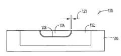
- FIG. 1Ashows a semiconductor substrate 100 with a junction 110 formed in a portion of the semiconductor substrate 100 .
- the junction 110is formed within a well region or pocket 112 that is also formed in a portion of the semiconductor substrate 100 .
- the junctionis formed by introducing a dopant element to a first region 114 using processes such as ion implantation. Processes such as ion implantation force high energy ions into a surface of the semiconductor substrate 100 or pocket 112 . A microstructure of the surface, after implantation, is damaged and the ions are not electrically activated within the region of the semiconductor substrate 100 or pocket 112 .
- Annealingalso drives diffusion of the dopant element from the first region 114 to a diffused region 116 .
- the diffused region 116yielded an unacceptable depth 117 as shown in FIG. 1A .
- FIG. 1Bshows a semiconductor substrate 100 with a junction 120 formed in a portion of the semiconductor substrate 100 . Similar to FIG. 1A , in one embodiment, the junction 120 is formed within a well region or pocket 122 that is also formed in a portion of the semiconductor substrate 100 . Using novel methods that will be described below, dopant elements are introduced to a first region 124 . Following an annealing procedure, dopant elements are driven by diffusion from the first region 124 to a diffused region 126 . As shown by FIG. 1B , the diffused region 127 shows a steeper diffusion profile with a smaller diffusion depth 127 . It should be noted that FIGS. 1A and 1B are diagrams for illustration of differences between junctions in prior configurations in contrast to junctions after using the methods described below. FIGS. 1A and 1B are not necessarily drawn to scale.
- Diffusionis normally thought of as occurring by the random motion of atoms with the energy being thermal, with the driving force being a function of temperature and concentration. Therefore the higher the temperature, the more rapid the diffusion rate.
- the rate of diffusion of one element in anotheris a function of not only temperature but other factors such as crystal defects, in a specimen.
- the rate of diffusion at grain boundariesmay be over an order of magnitude greater than that in the bulk material.
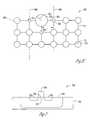
- FIG. 2Ashows one embodiment of a host semiconductor lattice 200 .
- the lattice 200is made up of a number of host atoms 210 that are held together by bonds 212 .
- the host semiconductor lattice 200is made up of silicon atoms.
- a silicon host semiconductor lattice 200is used as an example, other host semiconductor lattice compositions such as gallium arsenide, etc. are within the scope of the invention.
- the host semiconductor lattice 200is structured in a regular patterned crystalline form. In a crystal, the bonds 212 are arranged in a regular pattern throughout the lattice 200 . For illustration purposes, the bonds 212 are shown with equal bond lengths 214 .
- all bonds 212are substantially the same length 214
- other embodimentsare included where bond lengths 214 vary within the lattice 200 to form an energetically favorable atomic stacking arrangement in the host lattice 200 .
- individual atoms 210can be described as hard spheres that can be stacked a number of ways. A number of regular patterns of atomic stacking are therefore possible, some with equal bond lengths 214 and some with repeating variations in bond lengths 214 , depending on the atomic composition and solid phase of the host matrix.
- Dopant elements used to form the junctions in a silicon transistorare substantial (i.e., occupy lattice sites normally occupied by Si atoms). Since the radii of dopant ions differ from that of a silicon host matrix, the resulting differences in size imparts strain to the doped silicon region. This strain becomes especially large as the dopant concentration is raised to the levels needed to form the necessary junctions.
- FIG. 2Billustrates the host matrix 200 from FIG. 2A with the addition of a dopant atom 220 .
- the dopant atom 220is located in a substitutional lattice site.
- the dopant atom 220causes lattice strain, thus distorting the regular pattern of the host lattice 200 that existed when the dopant atom 220 was not present.
- Host atom 230has been moved from an unstrained position on line 232 to a strained location, thus distorting bonds 234 and 236 .
- other host atoms and bondsare similarly distorted.
- the effect of lattice strainis not limited to the host atoms directly adjacent to the dopant atom 220 .
- Host atom 240has been moved from an unstrained position on line 242 to a strained location, thus distorting bonds 244 and 246 .
- FIG. 2Bshows a dopant atom 220 with an atomic radius that is larger than the atomic radius of the host matrix atoms
- a dopant atom 220 with an atomic radius that is smaller than the atomic radius of the host matrix atomscauses similar lattice distortion. Instead of the bonds such as 234 and 236 being compressed, the bonds adjacent to a smaller dopant atom are stretched, thus causing host lattice distortion. It has been discovered that such dopant-induced strains provide a driving force to cause enhanced, non-random diffusion effects. To reduce unwanted diffusion, it therefore follows that the net lattice strain in a junction should be at or near zero. In one embodiment, this can be achieved by using two or more dopants of the same type in each junction with at least one of the dopants having an atomic size smaller and one larger than silicon. The percentages of each being so chosen that the net size effect approaches zero.
- FIG. 2Cshows the host matrix 200 from FIGS. 2A , and 2 B with the addition of multiple dopant atoms.
- the multiple dopant atomsinclude a first dopant atom 250 with an atomic radius 251 that is larger that at atomic radius 211 of host atoms 210 .
- the multiple dopant atomsfurther include a second dopant atom 260 with an atomic radius 261 that is smaller that the atomic radius 211 of host atoms 210 .
- the multiple dopant atomsinclude P-type dopant atoms.
- the multiple dopant atomsinclude N-type dopant atoms.
- N-type dopant atomsinclude, but are not limited to, arsenic (As), phosphorous (P), Bismuth (Bi), and Antimony (Sb).
- P-type dopant atomsinclude, but are not limited to, Aluminum (Al) and Boron (B).
- FIG. 2Cshows a host lattice 200 with two different dopant atoms, other embodiments include more than two different dopant atoms.
- a specific proportion of dopant atomsis further chosen for introduction to the lattice 200 .
- strain in the lattice 200is reduced significantly.
- the larger radius 251 of the first dopant atom 250complements the smaller radius 261 of the second dopant atom 260 .
- atoms in the lattice, including both host matrix atoms and dopant atomsare substantially lined up as in the unstressed state of FIG. 2A .
- Dopant atom 260is shown along substantially undistorted lines 264 and 268
- dopant atom 261is shown along substantially undistorted lines 266 and 268
- selected bondssuch as bond 262 in the doped lattice 200 of FIG. 2C may be shorter or longer than host matrix bonds 212
- a center to center spacing 265is approximately equal to the length of host matrix bonds 212 .
- FIG. 2Cshows the larger first dopant atom 250 bonded adjacent to the smaller second dopant atom 260 this specific configuration is for illustration only.
- lattice strainis minimized regardless of which host lattice sites the multiple dopant atoms are located on.
- Small dopant atomsdo not necessarily have to be directly bonded to large dopant atoms.
- an average lattice strainis reduced due to the size of dopant atoms selected and the proportion in which they are introduced.
- R hthe atomic radius of a host atom
- R lthe atomic radius of the dopant atom that is larger than the host atom
- R sthe atomic radius of the dopant atom that is smaller than the host atom
- the host atomhas a relative radius of 2
- the large dopant atomhas a relative radius of 6
- the small dopant atomhas a relative radius of 1
- “x”would equal 0.20
- “1 ⁇ x”would equal 0.80.
- a resulting dopant proportionwould include one large dopant atom for every four small dopant atoms.
- the proportion of dopant atoms that are larger than the host matrix atomsshould compensate for the proportions of dopant atoms that are smaller that the host matrix atoms, while taking into consideration the relative sizes of the dopant atoms and the host matrix atoms.
- both arsenic (As) and phosphorous (P)are used as dopants.
- Asarsenic
- Pphosphorous
- both boron (B) and aluminum (Al)are used as dopants.
- Bboron
- Alaluminum
- introduction of the multiple dopant atoms to the host lattice 200includes an ion implantation process. As discussed above, following ion implantation, there is damage to the host lattice that must be repaired. Further, the implanted dopant atoms must be activated to realize their desired electrical properties. In one embodiment, an anneal step is performed following introduction of the dopant atoms to the host lattice. In one embodiment, a rapid thermal anneal process is used following introduction of the dopant atoms to the host lattice. By choosing a combination of multiple dopant atoms, introduced to a host lattice at a specific proportion as described above, the post anneal doped region exhibits significantly reduced lattice strain. The reduced lattice strain significantly reduces unwanted enhanced, non-random diffusion effects.
- One advantage of methods described aboveis that the methods effectively reduce the rate of diffusion of the doping elements in very shallow junctions so that they can be exposed to a higher time temperature envelope without excessive degradation of the structure. Another advantage of methods described above is that the methods sharpen a junction profile by reducing diffusion rates at current anneal times and temperatures. A further advantage of methods described above is that solubility in doped regions will be increased. Thus allowing for a higher maximum doping level.
- FIG. 3shows one example of a device that is formed using the methods described above.
- FIG. 3shows a transistor 300 formed in a semiconductor substrate 310 . Other devices apart from transistors may also be formed using the methods described above.
- the transistoris further formed in a doped pocket 320 .
- the transistor 300includes a first source/drain region 330 , a second source drain region 332 , and a channel region 334 separating the first and second source/drain regions 330 , 332 .
- a gate 338is formed over the channel region 334 , with a gate oxide 336 separating the channel region 334 from the gate 338 .
- the first and second source/drain regions 330 , 332are formed using the multiple dopant implant methods described above. In one embodiment including a doped pocket 320 , the doped pocket 320 is also formed using the multiple dopant methods described above. In one embodiment, the doped pocket 320 is formed using multiple dopant atoms of a type that is complementary to the source/drain regions. In one embodiment, the source/drain regions 330 / 332 include P-type dopant atoms, and the pocket 320 includes N-type dopant atoms. In one embodiment, the source/drain regions 330 / 332 include N-type dopant atoms, and the pocket 320 includes P-type dopant atoms.
- the P pocketwould be constructed using a 135 KEV aluminum and a 60 KEV boron deposition. If the total concentration of the pocket was to be 10 20 , then a 0.7632 ⁇ 10 20 aluminum deposition would be used and a 0.2368 ⁇ 10 20 boron deposition would be used.
- the 500 Angstrom N-type junctionwould be constructed using a 40 KEV phosphorus and a 70 KEV arsenic deposition. It the total concentration of the diffusion was to be 5 ⁇ 10 20 , then the phosphorus concentration would be 1.82 ⁇ 10 20 and the arsenic concentration would be 3.18 ⁇ 10 20 .
- junctionscan be used to form devices that include, but are not limited to transistors, capacitors, etc.
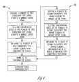
- FIG. 4shows a flow diagram of a method of fabricating a junction in a semiconductor device.
- a first flow 400includes operations for forming a region using multiple dopant atoms to reduce lattice strain as described in embodiments above.
- a second flow 410is included in one embodiment to include forming a doped region within another doped region. Both methods are effective to significantly reduce diffusion rates of dopant elements during processing steps such as annealing.
- FIG. 5Semiconducting wafers, semiconductor devices, and IC's created by the methods described above may be implemented into memory devices and information handling devices as shown in FIG. 5 , FIG. 6 , and FIG. 7 and as described below. While specific types of memory devices and computing devices are shown below, it will be recognized by one skilled in the art that several types of memory devices and information handling devices could utilize the invention.
- a personal computerincludes a monitor 500 , keyboard input 502 and a central processing unit 504 .
- the processor unittypically includes microprocessor 606 , memory bus circuit 608 having a plurality of memory slots 612 ( a - n ), and other peripheral circuitry 610 .
- Peripheral circuitry 610permits various peripheral devices 624 to interface processor-memory bus 620 over input/output (I/O) bus 622 .
- the personal computer shown in FIGS. 5 and 6also includes at least one transistor having a gate oxide according to the teachings of the present invention.
- Microprocessor 606produces control and address signals to control the exchange of data between memory bus circuit 608 and microprocessor 606 and between memory bus circuit 608 and peripheral circuitry 610 . This exchange of data is accomplished over high speed memory bus 620 and over high speed I/O bus 622 .
- Coupled to memory bus 620are a plurality of memory slots 612 ( a - n ) which receive memory devices well known to those skilled in the art.
- memory slots 612a - n
- SIMMssingle in-line memory modules
- DIMMsdual in-line memory modules
- Page mode operations in a DRAMare defined by the method of accessing a row of a memory cell arrays and randomly accessing different columns of the array. Data stored at the row and column intersection can be read and output while that column is accessed. Page mode DRAMs require access steps which limit the communication speed of memory circuit 608 . A typical communication speed for a DRAM device using page mode is approximately 33 MHZ.
- EDOextended data output
- DDR SDRAMDDR SDRAM
- SLDRAMDirect RDRAM
- SRAMFlash memories
- FIG. 7is a block diagram of an illustrative DRAM device 700 compatible with memory slots 612 ( a - n ).
- the description of DRAM 700has been simplified for purposes of illustrating a DRAM memory device and is not intended to be a complete description of all the features of a DRAM. Those skilled in the art will recognize that a wide variety of memory devices may be used in the implementation of the present invention.
- the example of a DRAM memory device shown in FIG. 7includes at least one transistor having a gate oxide according to the teachings of the present invention.
- Control, address and data information provided over memory bus 620is further represented by individual inputs to DRAM 700 , as shown in FIG. 7 . These individual representations are illustrated by data lines 702 , address lines 704 and various discrete lines directed to control logic 706 .
- DRAM 700includes memory array 710 which in turn comprises rows and columns of addressable memory cells. Each memory cell in a row is coupled to a common wordline. Additionally, each memory cell in a column is coupled to a common bitline. Each cell in memory array 710 includes a storage capacitor and an access transistor as is conventional in the art.
- DRAM 700interfaces with, for example, microprocessor 606 through address lines 704 and data lines 702 .
- DRAM 700may interface with a DRAM controller, a micro-controller, a chip set or other electronic system.
- Microprocessor 606also provides a number of control signals to DRAM 700 , including but not limited to, row and column address strobe signals RAS and CAS, write enable signal WE, an output enable signal OE and other conventional control signals.
- Row address buffer 712 and row decoder 714receive and decode row addresses from row address signals provided on address lines 704 by microprocessor 606 . Each unique row address corresponds to a row of cells in memory array 710 .
- Row decoder 714includes a wordline driver, an address decoder tree, and circuitry which translates a given row address received from row address buffers 712 and selectively activates the appropriate wordline of memory array 710 via the wordline drivers.
- Column address buffer 716 and column decoder 718receive and decode column address signals provided on address lines 704 .
- Column decoder 718also determines when a column is defective and the address of a replacement column.
- Column decoder 718is coupled to sense amplifiers 720 .
- Sense amplifiers 720are coupled to complementary pairs of bitlines of memory array 710 .
- Sense amplifiers 720are coupled to data-in buffer 722 and data-out buffer 724 .
- Data-in buffers 722 and data-out buffers 724are coupled to data lines 702 .
- data lines 702provide data to data-in buffer 722 .
- Sense amplifier 720receives data from data-in buffer 722 and stores the data in memory array 710 as a charge on a capacitor of a cell at an address specified on address lines 704 .
- DRAM 700transfers data to microprocessor 606 from memory array 710 .
- Complementary bitlines for the accessed cellare equilibrated during a precharge operation to a reference voltage provided by an equilibration circuit and a reference voltage supply.
- the charge stored in the accessed cellis then shared with the associated bitlines.
- a sense amplifier of sense amplifiers 720detects and amplifies a difference in voltage between the complementary bitlines.
- the sense amplifierpasses the amplified voltage to data-out buffer 724 .
- Control logic 706is used to control the many available functions of DRAM 700 .
- various control circuits and signals not detailed hereininitiate and synchronize DRAM 700 operation as known to those skilled in the art.
- the description of DRAM 700has been simplified for purposes of illustrating the present invention and is not intended to be a complete description of all the features of a DRAM.
- Devices and methods described aboveinclude advantages such as effective reduction in the rate of diffusion of the doping elements in very shallow junctions.
- the junctionscan be exposed to a higher time temperature envelope without excessive degradation of the structure.
- Another advantage of devices and methods described aboveis that the methods sharpen a junction profile by reducing diffusion rates at current anneal times and temperatures.
- a further advantage of devices and methods described aboveis that solubility in doped regions will be increased. Thus allowing for a higher maximum doping level.
- junctionscan be used to form devices that include, but are not limited to transistors, capacitors, etc.
Landscapes
- Physics & Mathematics (AREA)
- Engineering & Computer Science (AREA)
- High Energy & Nuclear Physics (AREA)
- General Physics & Mathematics (AREA)
- Toxicology (AREA)
- Condensed Matter Physics & Semiconductors (AREA)
- Health & Medical Sciences (AREA)
- Manufacturing & Machinery (AREA)
- Computer Hardware Design (AREA)
- Microelectronics & Electronic Packaging (AREA)
- Power Engineering (AREA)
- Insulated Gate Type Field-Effect Transistor (AREA)
- Metal-Oxide And Bipolar Metal-Oxide Semiconductor Integrated Circuits (AREA)
Abstract
Description
x=(Rh−Rs)/[(Rl−Rh)+(Rh−Rs)]
Claims (23)
Priority Applications (2)
| Application Number | Priority Date | Filing Date | Title |
|---|---|---|---|
| US11/214,555US7727868B2 (en) | 2002-12-20 | 2005-08-30 | Apparatus and method for controlling diffusion |
| US12/790,574US9147735B2 (en) | 2002-12-20 | 2010-05-28 | Apparatus and method for controlling diffusion |
Applications Claiming Priority (2)
| Application Number | Priority Date | Filing Date | Title |
|---|---|---|---|
| US10/326,935US20040121524A1 (en) | 2002-12-20 | 2002-12-20 | Apparatus and method for controlling diffusion |
| US11/214,555US7727868B2 (en) | 2002-12-20 | 2005-08-30 | Apparatus and method for controlling diffusion |
Related Parent Applications (1)
| Application Number | Title | Priority Date | Filing Date |
|---|---|---|---|
| US10/326,935DivisionUS20040121524A1 (en) | 2002-12-20 | 2002-12-20 | Apparatus and method for controlling diffusion |
Related Child Applications (1)
| Application Number | Title | Priority Date | Filing Date |
|---|---|---|---|
| US12/790,574ContinuationUS9147735B2 (en) | 2002-12-20 | 2010-05-28 | Apparatus and method for controlling diffusion |
Publications (2)
| Publication Number | Publication Date |
|---|---|
| US20060003535A1 US20060003535A1 (en) | 2006-01-05 |
| US7727868B2true US7727868B2 (en) | 2010-06-01 |
Family
ID=32594135
Family Applications (4)
| Application Number | Title | Priority Date | Filing Date |
|---|---|---|---|
| US10/326,935AbandonedUS20040121524A1 (en) | 2002-12-20 | 2002-12-20 | Apparatus and method for controlling diffusion |
| US11/215,466Expired - LifetimeUS7592242B2 (en) | 2002-12-20 | 2005-08-30 | Apparatus and method for controlling diffusion |
| US11/214,555Expired - LifetimeUS7727868B2 (en) | 2002-12-20 | 2005-08-30 | Apparatus and method for controlling diffusion |
| US12/790,574Expired - LifetimeUS9147735B2 (en) | 2002-12-20 | 2010-05-28 | Apparatus and method for controlling diffusion |
Family Applications Before (2)
| Application Number | Title | Priority Date | Filing Date |
|---|---|---|---|
| US10/326,935AbandonedUS20040121524A1 (en) | 2002-12-20 | 2002-12-20 | Apparatus and method for controlling diffusion |
| US11/215,466Expired - LifetimeUS7592242B2 (en) | 2002-12-20 | 2005-08-30 | Apparatus and method for controlling diffusion |
Family Applications After (1)
| Application Number | Title | Priority Date | Filing Date |
|---|---|---|---|
| US12/790,574Expired - LifetimeUS9147735B2 (en) | 2002-12-20 | 2010-05-28 | Apparatus and method for controlling diffusion |
Country Status (1)
| Country | Link |
|---|---|
| US (4) | US20040121524A1 (en) |
Cited By (1)
| Publication number | Priority date | Publication date | Assignee | Title |
|---|---|---|---|---|
| US20100237422A1 (en)* | 2002-12-20 | 2010-09-23 | Farrar Paul A | Apparatus and method for controlling diffusion |
Families Citing this family (4)
| Publication number | Priority date | Publication date | Assignee | Title |
|---|---|---|---|---|
| US7297617B2 (en)* | 2003-04-22 | 2007-11-20 | Micron Technology, Inc. | Method for controlling diffusion in semiconductor regions |
| US7172949B2 (en)* | 2004-08-09 | 2007-02-06 | Micron Technology, Inc. | Epitaxial semiconductor layer and method |
| JP6054606B2 (en)* | 2012-01-26 | 2016-12-27 | トヨタ自動車株式会社 | Thermoelectric semiconductor |
| DE102018111213A1 (en)* | 2018-05-09 | 2019-11-14 | Infineon Technologies Ag | Semiconductor device and manufacturing method |
Citations (58)
| Publication number | Priority date | Publication date | Assignee | Title |
|---|---|---|---|---|
| US3082131A (en)* | 1959-01-16 | 1963-03-19 | Texas Instruments Inc | Versatile transistor structure |
| US3748198A (en) | 1970-01-22 | 1973-07-24 | Ibm | Simultaneous double diffusion into a semiconductor substrate |
| US3812519A (en)* | 1970-02-07 | 1974-05-21 | Tokyo Shibaura Electric Co | Silicon double doped with p and as or b and as |
| US3886569A (en) | 1970-01-22 | 1975-05-27 | Ibm | Simultaneous double diffusion into a semiconductor substrate |
| US4111719A (en) | 1976-12-06 | 1978-09-05 | International Business Machines Corporation | Minimization of misfit dislocations in silicon by double implantation of arsenic and germanium |
| US4155785A (en) | 1976-01-28 | 1979-05-22 | International Business Machines Corporation | Process of making a radiation responsive device |
| US4332627A (en) | 1979-04-30 | 1982-06-01 | International Business Machines Corporation | Method of eliminating lattice defects in a semiconductor device |
| US4369072A (en) | 1981-01-22 | 1983-01-18 | International Business Machines Corp. | Method for forming IGFET devices having improved drain voltage characteristics |
| US4507159A (en) | 1981-10-07 | 1985-03-26 | Advanced Micro Devices, Inc. | Method of manufacturing high capacity semiconductor capacitance devices |
| US4569697A (en) | 1983-08-26 | 1986-02-11 | Energy Conversion Devices, Inc. | Method of forming photovoltaic quality amorphous alloys by passivating defect states |
| US4629520A (en) | 1983-08-30 | 1986-12-16 | Fujitsu Limited | Method of forming shallow n-type region with arsenic or antimony and phosphorus |
| US4746964A (en) | 1986-08-28 | 1988-05-24 | Fairchild Semiconductor Corporation | Modification of properties of p-type dopants with other p-type dopants |
| US4769689A (en) | 1984-12-13 | 1988-09-06 | American Telephone And Telegraph Company, At&T Bell Laboratories | Stress relief in epitaxial wafers |
| US4778772A (en) | 1977-06-09 | 1988-10-18 | Kabushiki Kaisha Toshiba | Method of manufacturing a bipolar transistor |
| US4851360A (en) | 1986-09-29 | 1989-07-25 | Texas Instruments Incorporated | NMOS source/drain doping with both P and As |
| US5021851A (en) | 1988-05-03 | 1991-06-04 | Texas Instruments Incorporated | NMOS source/drain doping with both P and As |
| US5060033A (en)* | 1988-08-18 | 1991-10-22 | Seiko Epson Corporation | Semiconductor device and method of producing semiconductor device |
| US5116455A (en) | 1991-01-24 | 1992-05-26 | Spire Corporation | Process of making strain-free, carbon-doped epitaxial layers and products so made |
| US5190887A (en)* | 1991-12-30 | 1993-03-02 | Intel Corporation | Method of making electrically erasable and electrically programmable memory cell with extended cycling endurance |
| US5212101A (en) | 1989-04-14 | 1993-05-18 | Secretary Of State For Defence In Her Britannic Majesty's Government Of The United Kingdom | Substitutional carbon in silicon |
| US5231298A (en) | 1991-01-24 | 1993-07-27 | Spire Corporation | GaAs device having a strain-free c-doped layer |
| US5245208A (en) | 1991-04-22 | 1993-09-14 | Mitsubishi Denki Kabushiki Kaisha | Semiconductor device and manufacturing method thereof |
| US5261999A (en) | 1991-05-08 | 1993-11-16 | North American Philips Corporation | Process for making strain-compensated bonded silicon-on-insulator material free of dislocations |
| US5280185A (en) | 1990-04-18 | 1994-01-18 | National Semiconductor Corporation | Application of electronic properties of germanium to inhibit n-type or p-type diffusion in silicon |
| US5281831A (en) | 1990-10-31 | 1994-01-25 | Kabushiki Kaisha Toshiba | Optical semiconductor device |
| US5311055A (en) | 1991-11-22 | 1994-05-10 | The United States Of America As Represented By The Secretary Of The Navy | Trenched bipolar transistor structures |
| US5345104A (en) | 1992-05-15 | 1994-09-06 | Micron Technology, Inc. | Flash memory cell having antimony drain for reduced drain voltage during programming |
| US5389809A (en) | 1982-02-01 | 1995-02-14 | Texas Instruments Incorporated | Silicided MOS transistor |
| US5510630A (en) | 1993-10-18 | 1996-04-23 | Westinghouse Electric Corporation | Non-volatile random access memory cell constructed of silicon carbide |
| US5561072A (en) | 1993-11-22 | 1996-10-01 | Nec Corporation | Method for producing shallow junction in surface region of semiconductor substrate using implantation of plasma ions |
| US5654210A (en)* | 1994-09-13 | 1997-08-05 | Lsi Logic Corporation | Process for making group IV semiconductor substrate treated with one or more group IV elements to form one or more barrier regions capable of inhibiting migration of dopant materials in substrate |
| US5789310A (en) | 1996-12-10 | 1998-08-04 | Advanced Micro Devices, Inc. | Method of forming shallow junctions by entrapment of interstitial atoms |
| US5814541A (en) | 1987-12-04 | 1998-09-29 | Kabushiki Kaisha Toshiba | Method for manufacturing semiconductor device |
| US5837597A (en) | 1994-12-21 | 1998-11-17 | Nec Corporation | Method of manufacturing semiconductor device with shallow impurity layers |
| US5937318A (en)* | 1985-11-19 | 1999-08-10 | Warner, Jr.; Raymond M. | Monocrystalline three-dimensional integrated circuit |
| US6037625A (en)* | 1997-12-08 | 2000-03-14 | Nec Corporation | Semiconductor device with salicide structure and fabrication method thereof |
| US6133082A (en) | 1998-08-28 | 2000-10-17 | Nec Corporation | Method of fabricating CMOS semiconductor device |
| US6198167B1 (en) | 1999-04-29 | 2001-03-06 | International Business Machines Corporation | Semiconductor structure exhibiting reduced contact resistance and method for fabrication |
| US6235599B1 (en) | 1999-10-25 | 2001-05-22 | Advanced Micro Devices, Inc. | Fabrication of a shallow doped junction having low sheet resistance using multiple implantations |
| US6258695B1 (en) | 1999-02-04 | 2001-07-10 | International Business Machines Corporation | Dislocation suppression by carbon incorporation |
| US6368928B1 (en) | 2001-06-12 | 2002-04-09 | Taiwan Semiconductor Manufacturing Company | Method of forming an indium retrograde profile via use of a low temperature anneal procedure to reduce NMOS short channel effects |
| US20020063294A1 (en) | 2000-03-30 | 2002-05-30 | International Business Machines | Reduction of reverse short channel effects by implantation of neutral dopants |
| US6437374B1 (en) | 2001-05-07 | 2002-08-20 | Xerox Corporation | Semiconductor device and method of forming a semiconductor device |
| US6455402B2 (en) | 1999-01-22 | 2002-09-24 | Hyundai Electronics Industries Co., Ltd. | Method of forming retrograde doping file in twin well CMOS device |
| US20030013260A1 (en) | 2001-07-16 | 2003-01-16 | Gossmann Hans-Joachim Ludwig | Increasing the electrical activation of ion-implanted dopants |
| US6518150B1 (en) | 1998-12-10 | 2003-02-11 | Oki Electric Industry Co., Ltd. | Method of manufacturing semiconductor device |
| US20030075806A1 (en) | 2001-10-22 | 2003-04-24 | Reber Douglas M. | Intergrated circuit having interconnect to a substrate and method therefor |
| US20030087510A1 (en) | 2001-11-06 | 2003-05-08 | Chen Aikwo Eric | Method of forming MOS transistor graded junctions using multiple implant of low diffusion specie, and a device formed thereby |
| US6576521B1 (en) | 1998-04-07 | 2003-06-10 | Agere Systems Inc. | Method of forming semiconductor device with LDD structure |
| US6589830B1 (en) | 2000-09-20 | 2003-07-08 | Fairchild Semiconductor Corporation | Self-aligned process for fabricating power MOSFET with spacer-shaped terraced gate |
| US6696341B1 (en) | 1998-01-21 | 2004-02-24 | Renesas Technology Corp. | Method of manufacturing a semiconductor device having electrostatic discharge protection element |
| US20040038468A1 (en) | 2002-06-20 | 2004-02-26 | Jack Hwang | Forming strained source drain junction field effect transistors |
| US6797593B2 (en) | 2002-09-13 | 2004-09-28 | Texas Instruments Incorporated | Methods and apparatus for improved mosfet drain extension activation |
| US20050026403A1 (en) | 2003-07-28 | 2005-02-03 | International Business Machines Corporation | Method for slowing down dopant-enhanced diffusion in substrates and devices fabricated therefrom |
| US6930360B2 (en) | 2002-09-24 | 2005-08-16 | Kabushiki Kaisha Toshiba | Semiconductor device and manufacturing method of the same |
| US6991972B2 (en) | 2002-10-22 | 2006-01-31 | Amberwave Systems Corporation | Gate material for semiconductor device fabrication |
| US7297617B2 (en) | 2003-04-22 | 2007-11-20 | Micron Technology, Inc. | Method for controlling diffusion in semiconductor regions |
| US7592242B2 (en) | 2002-12-20 | 2009-09-22 | Micron Technology, Inc. | Apparatus and method for controlling diffusion |
Family Cites Families (6)
| Publication number | Priority date | Publication date | Assignee | Title |
|---|---|---|---|---|
| DE2107252C3 (en)* | 1971-02-16 | 1980-06-26 | Paul 8501 Oberasbach Unger | Arrangement that can be used for sports equipment for setting and displaying the force of a spring |
| US4364778A (en)* | 1980-05-30 | 1982-12-21 | Bell Telephone Laboratories, Incorporated | Formation of multilayer dopant distributions in a semiconductor |
| US5349225A (en)* | 1993-04-12 | 1994-09-20 | Texas Instruments Incorporated | Field effect transistor with a lightly doped drain |
| JP3239202B2 (en)* | 1995-12-01 | 2001-12-17 | シャープ株式会社 | MOS transistor and method of manufacturing the same |
| US6038625A (en)* | 1998-01-06 | 2000-03-14 | Sony Corporation Of Japan | Method and system for providing a device identification mechanism within a consumer audio/video network |
| US6452236B1 (en)* | 2001-05-31 | 2002-09-17 | Texas Instruments, Incorporated | Channel implant for improving NMOS ESD robustness |
- 2002
- 2002-12-20USUS10/326,935patent/US20040121524A1/ennot_activeAbandoned
- 2005
- 2005-08-30USUS11/215,466patent/US7592242B2/ennot_activeExpired - Lifetime
- 2005-08-30USUS11/214,555patent/US7727868B2/ennot_activeExpired - Lifetime
- 2010
- 2010-05-28USUS12/790,574patent/US9147735B2/ennot_activeExpired - Lifetime
Patent Citations (63)
| Publication number | Priority date | Publication date | Assignee | Title |
|---|---|---|---|---|
| US3082131A (en)* | 1959-01-16 | 1963-03-19 | Texas Instruments Inc | Versatile transistor structure |
| US3748198A (en) | 1970-01-22 | 1973-07-24 | Ibm | Simultaneous double diffusion into a semiconductor substrate |
| US3886569A (en) | 1970-01-22 | 1975-05-27 | Ibm | Simultaneous double diffusion into a semiconductor substrate |
| US3812519A (en)* | 1970-02-07 | 1974-05-21 | Tokyo Shibaura Electric Co | Silicon double doped with p and as or b and as |
| US4155785A (en) | 1976-01-28 | 1979-05-22 | International Business Machines Corporation | Process of making a radiation responsive device |
| US4137103A (en) | 1976-12-06 | 1979-01-30 | International Business Machines Corporation | Silicon integrated circuit region containing implanted arsenic and germanium |
| US4111719A (en) | 1976-12-06 | 1978-09-05 | International Business Machines Corporation | Minimization of misfit dislocations in silicon by double implantation of arsenic and germanium |
| US4778772A (en) | 1977-06-09 | 1988-10-18 | Kabushiki Kaisha Toshiba | Method of manufacturing a bipolar transistor |
| US4332627A (en) | 1979-04-30 | 1982-06-01 | International Business Machines Corporation | Method of eliminating lattice defects in a semiconductor device |
| US4369072A (en) | 1981-01-22 | 1983-01-18 | International Business Machines Corp. | Method for forming IGFET devices having improved drain voltage characteristics |
| US4507159A (en) | 1981-10-07 | 1985-03-26 | Advanced Micro Devices, Inc. | Method of manufacturing high capacity semiconductor capacitance devices |
| US5389809A (en) | 1982-02-01 | 1995-02-14 | Texas Instruments Incorporated | Silicided MOS transistor |
| US4569697A (en) | 1983-08-26 | 1986-02-11 | Energy Conversion Devices, Inc. | Method of forming photovoltaic quality amorphous alloys by passivating defect states |
| US4875085A (en) | 1983-08-30 | 1989-10-17 | Fujitsu Limited | Semiconductor device with shallow n-type region with arsenic or antimony and phosphorus |
| US4629520A (en) | 1983-08-30 | 1986-12-16 | Fujitsu Limited | Method of forming shallow n-type region with arsenic or antimony and phosphorus |
| US4769689A (en) | 1984-12-13 | 1988-09-06 | American Telephone And Telegraph Company, At&T Bell Laboratories | Stress relief in epitaxial wafers |
| US5937318A (en)* | 1985-11-19 | 1999-08-10 | Warner, Jr.; Raymond M. | Monocrystalline three-dimensional integrated circuit |
| US4746964A (en) | 1986-08-28 | 1988-05-24 | Fairchild Semiconductor Corporation | Modification of properties of p-type dopants with other p-type dopants |
| US4851360A (en) | 1986-09-29 | 1989-07-25 | Texas Instruments Incorporated | NMOS source/drain doping with both P and As |
| US5814541A (en) | 1987-12-04 | 1998-09-29 | Kabushiki Kaisha Toshiba | Method for manufacturing semiconductor device |
| US5021851A (en) | 1988-05-03 | 1991-06-04 | Texas Instruments Incorporated | NMOS source/drain doping with both P and As |
| US5060033A (en)* | 1988-08-18 | 1991-10-22 | Seiko Epson Corporation | Semiconductor device and method of producing semiconductor device |
| US5212101A (en) | 1989-04-14 | 1993-05-18 | Secretary Of State For Defence In Her Britannic Majesty's Government Of The United Kingdom | Substitutional carbon in silicon |
| US5280185A (en) | 1990-04-18 | 1994-01-18 | National Semiconductor Corporation | Application of electronic properties of germanium to inhibit n-type or p-type diffusion in silicon |
| US5281831A (en) | 1990-10-31 | 1994-01-25 | Kabushiki Kaisha Toshiba | Optical semiconductor device |
| US5231298A (en) | 1991-01-24 | 1993-07-27 | Spire Corporation | GaAs device having a strain-free c-doped layer |
| US5116455A (en) | 1991-01-24 | 1992-05-26 | Spire Corporation | Process of making strain-free, carbon-doped epitaxial layers and products so made |
| US5245208A (en) | 1991-04-22 | 1993-09-14 | Mitsubishi Denki Kabushiki Kaisha | Semiconductor device and manufacturing method thereof |
| US5261999A (en) | 1991-05-08 | 1993-11-16 | North American Philips Corporation | Process for making strain-compensated bonded silicon-on-insulator material free of dislocations |
| US5311055A (en) | 1991-11-22 | 1994-05-10 | The United States Of America As Represented By The Secretary Of The Navy | Trenched bipolar transistor structures |
| US5190887A (en)* | 1991-12-30 | 1993-03-02 | Intel Corporation | Method of making electrically erasable and electrically programmable memory cell with extended cycling endurance |
| US5345104A (en) | 1992-05-15 | 1994-09-06 | Micron Technology, Inc. | Flash memory cell having antimony drain for reduced drain voltage during programming |
| US5510630A (en) | 1993-10-18 | 1996-04-23 | Westinghouse Electric Corporation | Non-volatile random access memory cell constructed of silicon carbide |
| US5561072A (en) | 1993-11-22 | 1996-10-01 | Nec Corporation | Method for producing shallow junction in surface region of semiconductor substrate using implantation of plasma ions |
| US5654210A (en)* | 1994-09-13 | 1997-08-05 | Lsi Logic Corporation | Process for making group IV semiconductor substrate treated with one or more group IV elements to form one or more barrier regions capable of inhibiting migration of dopant materials in substrate |
| US5837597A (en) | 1994-12-21 | 1998-11-17 | Nec Corporation | Method of manufacturing semiconductor device with shallow impurity layers |
| US5789310A (en) | 1996-12-10 | 1998-08-04 | Advanced Micro Devices, Inc. | Method of forming shallow junctions by entrapment of interstitial atoms |
| US6037625A (en)* | 1997-12-08 | 2000-03-14 | Nec Corporation | Semiconductor device with salicide structure and fabrication method thereof |
| US6696341B1 (en) | 1998-01-21 | 2004-02-24 | Renesas Technology Corp. | Method of manufacturing a semiconductor device having electrostatic discharge protection element |
| US6576521B1 (en) | 1998-04-07 | 2003-06-10 | Agere Systems Inc. | Method of forming semiconductor device with LDD structure |
| US6133082A (en) | 1998-08-28 | 2000-10-17 | Nec Corporation | Method of fabricating CMOS semiconductor device |
| US6518150B1 (en) | 1998-12-10 | 2003-02-11 | Oki Electric Industry Co., Ltd. | Method of manufacturing semiconductor device |
| US6455402B2 (en) | 1999-01-22 | 2002-09-24 | Hyundai Electronics Industries Co., Ltd. | Method of forming retrograde doping file in twin well CMOS device |
| US6258695B1 (en) | 1999-02-04 | 2001-07-10 | International Business Machines Corporation | Dislocation suppression by carbon incorporation |
| US6198167B1 (en) | 1999-04-29 | 2001-03-06 | International Business Machines Corporation | Semiconductor structure exhibiting reduced contact resistance and method for fabrication |
| US6235599B1 (en) | 1999-10-25 | 2001-05-22 | Advanced Micro Devices, Inc. | Fabrication of a shallow doped junction having low sheet resistance using multiple implantations |
| US20020063294A1 (en) | 2000-03-30 | 2002-05-30 | International Business Machines | Reduction of reverse short channel effects by implantation of neutral dopants |
| US6589830B1 (en) | 2000-09-20 | 2003-07-08 | Fairchild Semiconductor Corporation | Self-aligned process for fabricating power MOSFET with spacer-shaped terraced gate |
| US6437374B1 (en) | 2001-05-07 | 2002-08-20 | Xerox Corporation | Semiconductor device and method of forming a semiconductor device |
| US6368928B1 (en) | 2001-06-12 | 2002-04-09 | Taiwan Semiconductor Manufacturing Company | Method of forming an indium retrograde profile via use of a low temperature anneal procedure to reduce NMOS short channel effects |
| US20030013260A1 (en) | 2001-07-16 | 2003-01-16 | Gossmann Hans-Joachim Ludwig | Increasing the electrical activation of ion-implanted dopants |
| US20030075806A1 (en) | 2001-10-22 | 2003-04-24 | Reber Douglas M. | Intergrated circuit having interconnect to a substrate and method therefor |
| US20030087510A1 (en) | 2001-11-06 | 2003-05-08 | Chen Aikwo Eric | Method of forming MOS transistor graded junctions using multiple implant of low diffusion specie, and a device formed thereby |
| US20040038468A1 (en) | 2002-06-20 | 2004-02-26 | Jack Hwang | Forming strained source drain junction field effect transistors |
| US6797593B2 (en) | 2002-09-13 | 2004-09-28 | Texas Instruments Incorporated | Methods and apparatus for improved mosfet drain extension activation |
| US6930360B2 (en) | 2002-09-24 | 2005-08-16 | Kabushiki Kaisha Toshiba | Semiconductor device and manufacturing method of the same |
| US6991972B2 (en) | 2002-10-22 | 2006-01-31 | Amberwave Systems Corporation | Gate material for semiconductor device fabrication |
| US7592242B2 (en) | 2002-12-20 | 2009-09-22 | Micron Technology, Inc. | Apparatus and method for controlling diffusion |
| US7297617B2 (en) | 2003-04-22 | 2007-11-20 | Micron Technology, Inc. | Method for controlling diffusion in semiconductor regions |
| US7301221B2 (en) | 2003-04-22 | 2007-11-27 | Micron Technology, Inc. | Controlling diffusion in doped semiconductor regions |
| US20080070392A1 (en) | 2003-04-22 | 2008-03-20 | Micron Technology, Inc. | Controlling diffusion in doped semiconductor regions |
| US7585753B2 (en) | 2003-04-22 | 2009-09-08 | Micron Technology, Inc. | Controlling diffusion in doped semiconductor regions |
| US20050026403A1 (en) | 2003-07-28 | 2005-02-03 | International Business Machines Corporation | Method for slowing down dopant-enhanced diffusion in substrates and devices fabricated therefrom |
Non-Patent Citations (4)
| Title |
|---|
| Darken, L S., et al., "Physical chemistry of metals", Book, Published New York, McGraw-Hill,(1953),74-90, 457-458. |
| Eldridge, J M., et al., "Lowering stresses in silicon due to the presence of high concentration of N-type dopant", IBM Technical Disclosure Bulletin, vol. 14, No. 10. (1972),3013-14. |
| Swalin, R. A., "Thermodynamics of solids", Book, Published New York, Wiley Series: Wiley series on the science and technology of materials,(1962),149-155. |
| Trumbore, F A., "Solid Solubilities of Impurity Elements in Germanium and Silicon", The Bell System Technical Journal, 39, I.M. Mackintosh unpublished data is quoted by F.A. Trumbore in this article., (1960),205-233. |
Cited By (2)
| Publication number | Priority date | Publication date | Assignee | Title |
|---|---|---|---|---|
| US20100237422A1 (en)* | 2002-12-20 | 2010-09-23 | Farrar Paul A | Apparatus and method for controlling diffusion |
| US9147735B2 (en) | 2002-12-20 | 2015-09-29 | Micron Technology, Inc. | Apparatus and method for controlling diffusion |
Also Published As
| Publication number | Publication date |
|---|---|
| US20100237422A1 (en) | 2010-09-23 |
| US7592242B2 (en) | 2009-09-22 |
| US9147735B2 (en) | 2015-09-29 |
| US20060003559A1 (en) | 2006-01-05 |
| US20040121524A1 (en) | 2004-06-24 |
| US20060003535A1 (en) | 2006-01-05 |
Similar Documents
| Publication | Publication Date | Title |
|---|---|---|
| US7585753B2 (en) | Controlling diffusion in doped semiconductor regions | |
| US6134175A (en) | Memory address decode array with vertical transistors | |
| US7326597B2 (en) | Gettering using voids formed by surface transformation | |
| US6958263B2 (en) | Methods of forming devices, constructions and systems comprising thyristors | |
| US6906354B2 (en) | T-RAM cell having a buried vertical thyristor and a pseudo-TFT transfer gate and method for fabricating the same | |
| US6492662B2 (en) | T-RAM structure having dual vertical devices and method for fabricating the same | |
| US20030006446A1 (en) | Memory address and decode circuits with ultra thin body transistors | |
| US9147735B2 (en) | Apparatus and method for controlling diffusion | |
| US20220246536A1 (en) | Integrated Assemblies and Methods of Forming Integrated Assemblies | |
| US7898062B2 (en) | Epitaxial semiconductor layer and method | |
| US7005342B2 (en) | Method to fabricate surface p-channel CMOS | |
| US20240164093A1 (en) | Integrated Assemblies and Methods of Forming Integrated Assemblies | |
| US20020130376A1 (en) | Method to reduce transistor channel length using SDOX | |
| US7321148B2 (en) | Capacitor constructions and rugged silicon-containing surfaces |
Legal Events
| Date | Code | Title | Description |
|---|---|---|---|
| STCF | Information on status: patent grant | Free format text:PATENTED CASE | |
| FPAY | Fee payment | Year of fee payment:4 | |
| AS | Assignment | Owner name:U.S. BANK NATIONAL ASSOCIATION, AS COLLATERAL AGENT, CALIFORNIA Free format text:SECURITY INTEREST;ASSIGNOR:MICRON TECHNOLOGY, INC.;REEL/FRAME:038669/0001 Effective date:20160426 Owner name:U.S. BANK NATIONAL ASSOCIATION, AS COLLATERAL AGEN Free format text:SECURITY INTEREST;ASSIGNOR:MICRON TECHNOLOGY, INC.;REEL/FRAME:038669/0001 Effective date:20160426 | |
| AS | Assignment | Owner name:MORGAN STANLEY SENIOR FUNDING, INC., AS COLLATERAL AGENT, MARYLAND Free format text:PATENT SECURITY AGREEMENT;ASSIGNOR:MICRON TECHNOLOGY, INC.;REEL/FRAME:038954/0001 Effective date:20160426 Owner name:MORGAN STANLEY SENIOR FUNDING, INC., AS COLLATERAL Free format text:PATENT SECURITY AGREEMENT;ASSIGNOR:MICRON TECHNOLOGY, INC.;REEL/FRAME:038954/0001 Effective date:20160426 | |
| AS | Assignment | Owner name:U.S. BANK NATIONAL ASSOCIATION, AS COLLATERAL AGENT, CALIFORNIA Free format text:CORRECTIVE ASSIGNMENT TO CORRECT THE REPLACE ERRONEOUSLY FILED PATENT #7358718 WITH THE CORRECT PATENT #7358178 PREVIOUSLY RECORDED ON REEL 038669 FRAME 0001. ASSIGNOR(S) HEREBY CONFIRMS THE SECURITY INTEREST;ASSIGNOR:MICRON TECHNOLOGY, INC.;REEL/FRAME:043079/0001 Effective date:20160426 Owner name:U.S. BANK NATIONAL ASSOCIATION, AS COLLATERAL AGEN Free format text:CORRECTIVE ASSIGNMENT TO CORRECT THE REPLACE ERRONEOUSLY FILED PATENT #7358718 WITH THE CORRECT PATENT #7358178 PREVIOUSLY RECORDED ON REEL 038669 FRAME 0001. ASSIGNOR(S) HEREBY CONFIRMS THE SECURITY INTEREST;ASSIGNOR:MICRON TECHNOLOGY, INC.;REEL/FRAME:043079/0001 Effective date:20160426 | |
| MAFP | Maintenance fee payment | Free format text:PAYMENT OF MAINTENANCE FEE, 8TH YEAR, LARGE ENTITY (ORIGINAL EVENT CODE: M1552) Year of fee payment:8 | |
| AS | Assignment | Owner name:JPMORGAN CHASE BANK, N.A., AS COLLATERAL AGENT, ILLINOIS Free format text:SECURITY INTEREST;ASSIGNORS:MICRON TECHNOLOGY, INC.;MICRON SEMICONDUCTOR PRODUCTS, INC.;REEL/FRAME:047540/0001 Effective date:20180703 Owner name:JPMORGAN CHASE BANK, N.A., AS COLLATERAL AGENT, IL Free format text:SECURITY INTEREST;ASSIGNORS:MICRON TECHNOLOGY, INC.;MICRON SEMICONDUCTOR PRODUCTS, INC.;REEL/FRAME:047540/0001 Effective date:20180703 | |
| AS | Assignment | Owner name:MICRON TECHNOLOGY, INC., IDAHO Free format text:RELEASE BY SECURED PARTY;ASSIGNOR:U.S. BANK NATIONAL ASSOCIATION, AS COLLATERAL AGENT;REEL/FRAME:047243/0001 Effective date:20180629 | |
| AS | Assignment | Owner name:MICRON TECHNOLOGY, INC., IDAHO Free format text:RELEASE BY SECURED PARTY;ASSIGNOR:MORGAN STANLEY SENIOR FUNDING, INC., AS COLLATERAL AGENT;REEL/FRAME:050937/0001 Effective date:20190731 | |
| AS | Assignment | Owner name:MICRON TECHNOLOGY, INC., IDAHO Free format text:RELEASE BY SECURED PARTY;ASSIGNOR:JPMORGAN CHASE BANK, N.A., AS COLLATERAL AGENT;REEL/FRAME:051028/0001 Effective date:20190731 Owner name:MICRON SEMICONDUCTOR PRODUCTS, INC., IDAHO Free format text:RELEASE BY SECURED PARTY;ASSIGNOR:JPMORGAN CHASE BANK, N.A., AS COLLATERAL AGENT;REEL/FRAME:051028/0001 Effective date:20190731 | |
| MAFP | Maintenance fee payment | Free format text:PAYMENT OF MAINTENANCE FEE, 12TH YEAR, LARGE ENTITY (ORIGINAL EVENT CODE: M1553); ENTITY STATUS OF PATENT OWNER: LARGE ENTITY Year of fee payment:12 |