US7727795B2 - Exponentially doped layers in inverted metamorphic multijunction solar cells - Google Patents
Exponentially doped layers in inverted metamorphic multijunction solar cellsDownload PDFInfo
- Publication number
- US7727795B2 US7727795B2US12/187,454US18745408AUS7727795B2US 7727795 B2US7727795 B2US 7727795B2US 18745408 AUS18745408 AUS 18745408AUS 7727795 B2US7727795 B2US 7727795B2
- Authority
- US
- United States
- Prior art keywords
- subcell
- base
- solar subcell
- solar
- band gap
- Prior art date
- Legal status (The legal status is an assumption and is not a legal conclusion. Google has not performed a legal analysis and makes no representation as to the accuracy of the status listed.)
- Active
Links
Images


Classifications
- H—ELECTRICITY
- H10—SEMICONDUCTOR DEVICES; ELECTRIC SOLID-STATE DEVICES NOT OTHERWISE PROVIDED FOR
- H10F—INORGANIC SEMICONDUCTOR DEVICES SENSITIVE TO INFRARED RADIATION, LIGHT, ELECTROMAGNETIC RADIATION OF SHORTER WAVELENGTH OR CORPUSCULAR RADIATION
- H10F10/00—Individual photovoltaic cells, e.g. solar cells
- H10F10/10—Individual photovoltaic cells, e.g. solar cells having potential barriers
- H10F10/14—Photovoltaic cells having only PN homojunction potential barriers
- H10F10/142—Photovoltaic cells having only PN homojunction potential barriers comprising multiple PN homojunctions, e.g. tandem cells
- H10F10/1425—Inverted metamorphic multi-junction [IMM] photovoltaic cells
- H—ELECTRICITY
- H10—SEMICONDUCTOR DEVICES; ELECTRIC SOLID-STATE DEVICES NOT OTHERWISE PROVIDED FOR
- H10F—INORGANIC SEMICONDUCTOR DEVICES SENSITIVE TO INFRARED RADIATION, LIGHT, ELECTROMAGNETIC RADIATION OF SHORTER WAVELENGTH OR CORPUSCULAR RADIATION
- H10F10/00—Individual photovoltaic cells, e.g. solar cells
- H10F10/10—Individual photovoltaic cells, e.g. solar cells having potential barriers
- H10F10/14—Photovoltaic cells having only PN homojunction potential barriers
- H10F10/144—Photovoltaic cells having only PN homojunction potential barriers comprising only Group III-V materials, e.g. GaAs,AlGaAs, or InP photovoltaic cells
- H—ELECTRICITY
- H10—SEMICONDUCTOR DEVICES; ELECTRIC SOLID-STATE DEVICES NOT OTHERWISE PROVIDED FOR
- H10F—INORGANIC SEMICONDUCTOR DEVICES SENSITIVE TO INFRARED RADIATION, LIGHT, ELECTROMAGNETIC RADIATION OF SHORTER WAVELENGTH OR CORPUSCULAR RADIATION
- H10F71/00—Manufacture or treatment of devices covered by this subclass
- H10F71/127—The active layers comprising only Group III-V materials, e.g. GaAs or InP
- H10F71/1272—The active layers comprising only Group III-V materials, e.g. GaAs or InP comprising at least three elements, e.g. GaAlAs or InGaAsP
- H—ELECTRICITY
- H10—SEMICONDUCTOR DEVICES; ELECTRIC SOLID-STATE DEVICES NOT OTHERWISE PROVIDED FOR
- H10F—INORGANIC SEMICONDUCTOR DEVICES SENSITIVE TO INFRARED RADIATION, LIGHT, ELECTROMAGNETIC RADIATION OF SHORTER WAVELENGTH OR CORPUSCULAR RADIATION
- H10F77/00—Constructional details of devices covered by this subclass
- H10F77/10—Semiconductor bodies
- H10F77/12—Active materials
- H10F77/124—Active materials comprising only Group III-V materials, e.g. GaAs
- H10F77/1243—Active materials comprising only Group III-V materials, e.g. GaAs characterised by the dopants
- H—ELECTRICITY
- H10—SEMICONDUCTOR DEVICES; ELECTRIC SOLID-STATE DEVICES NOT OTHERWISE PROVIDED FOR
- H10F—INORGANIC SEMICONDUCTOR DEVICES SENSITIVE TO INFRARED RADIATION, LIGHT, ELECTROMAGNETIC RADIATION OF SHORTER WAVELENGTH OR CORPUSCULAR RADIATION
- H10F77/00—Constructional details of devices covered by this subclass
- H10F77/10—Semiconductor bodies
- H10F77/12—Active materials
- H10F77/124—Active materials comprising only Group III-V materials, e.g. GaAs
- H10F77/1248—Active materials comprising only Group III-V materials, e.g. GaAs having three or more elements, e.g. GaAlAs, InGaAs or InGaAsP
- Y—GENERAL TAGGING OF NEW TECHNOLOGICAL DEVELOPMENTS; GENERAL TAGGING OF CROSS-SECTIONAL TECHNOLOGIES SPANNING OVER SEVERAL SECTIONS OF THE IPC; TECHNICAL SUBJECTS COVERED BY FORMER USPC CROSS-REFERENCE ART COLLECTIONS [XRACs] AND DIGESTS
- Y02—TECHNOLOGIES OR APPLICATIONS FOR MITIGATION OR ADAPTATION AGAINST CLIMATE CHANGE
- Y02E—REDUCTION OF GREENHOUSE GAS [GHG] EMISSIONS, RELATED TO ENERGY GENERATION, TRANSMISSION OR DISTRIBUTION
- Y02E10/00—Energy generation through renewable energy sources
- Y02E10/50—Photovoltaic [PV] energy
- Y02E10/544—Solar cells from Group III-V materials
- Y—GENERAL TAGGING OF NEW TECHNOLOGICAL DEVELOPMENTS; GENERAL TAGGING OF CROSS-SECTIONAL TECHNOLOGIES SPANNING OVER SEVERAL SECTIONS OF THE IPC; TECHNICAL SUBJECTS COVERED BY FORMER USPC CROSS-REFERENCE ART COLLECTIONS [XRACs] AND DIGESTS
- Y02—TECHNOLOGIES OR APPLICATIONS FOR MITIGATION OR ADAPTATION AGAINST CLIMATE CHANGE
- Y02P—CLIMATE CHANGE MITIGATION TECHNOLOGIES IN THE PRODUCTION OR PROCESSING OF GOODS
- Y02P70/00—Climate change mitigation technologies in the production process for final industrial or consumer products
- Y02P70/50—Manufacturing or production processes characterised by the final manufactured product
Definitions
- the present inventionrelates to the field of solar cell semiconductor devices, and particularly to multifunction solar cells including a metamorphic layer. Such devices also include solar cells known as inverted metamorphic solar cells.
- Photovoltaic cellsalso called solar cells
- solar cellsare one of the most important new energy sources that have become available in the past several years. Considerable effort has gone into solar cell development. As a result, solar cells are currently being used in a number of commercial and consumer-oriented applications. While significant progress has been made in this area, the requirement for solar cells to meet the needs of more sophisticated applications has not kept pace with demand. Applications such as satellites used in data communications have dramatically increased the demand for solar cells with improved power and energy conversion characteristics.
- the size, mass and cost of a satellite power systemare dependent on the power and energy conversion efficiency of the solar cells used. Putting it another way, the size of the payload and the availability of on-board services are proportional to the amount of power provided.
- solar cellswhich act as the power conversion devices for the on-board power systems, become increasingly more important.
- Solar cellsare often fabricated in vertical, multijunction structures, and disposed in horizontal arrays, with the individual solar cells connected together in a series.
- the shape and structure of an array, as well as the number of cells it contains,are determined in part by the desired output voltage and current.
- Inverted metamorphic solar cell structuressuch as described in M. W. Wanlass et al., Lattice Mismatched Approaches for High Performance, III-V Photovoltaic Energy Converters (Conference Proceedings of the 31 st IEEE Photovoltaic Specialists Conference, Jan. 3-7, 2005, IEEE Press, 2005) present an important starting point for the development of future commercial high efficiency solar cells.
- the structures described in such prior artpresent a number of practical difficulties relating to the appropriate choice of materials and fabrication steps.
- the present inventionin one embodiment provides a method of forming a multijunction solar cell comprising an upper subcell, a middle subcell, and a lower subcell, the method comprising: providing first substrate for the epitaxial growth of semiconductor material; forming a first solar subcell having a base and an emitter on said substrate having a first band gap; forming a second solar subcell having a base and an emitter over said first solar subcell having a second band gap smaller than said first band gap; forming a grading interlayer over said second subcell, said grading interlayer having a third band gap greater than said second band gap; and forming a third solar subcell having a base and an emitter over said grading interlayer having a fourth band gap smaller than said second band gap such that said third subcell is lattice mismatched with respect to said second subcell, wherein at least one of the bases has an exponentially doped profile.
- the present inventionprovides an embodiment of a method of manufacturing a solar cell by providing a first substrate, depositing on the first substrate a sequence of layers of semiconductor material forming a solar cell, including at least one base layer with exponential doping; mounting a surrogate substrate on top of the sequence of layers; and removing the first substrate.
- the present inventionprovides an embodiment of a method of manufacturing a solar cell by providing a first substrate, depositing on the first substrate a sequence of layers of semiconductor material forming a solar cell, including at least one base layer with exponential doping; mounting a surrogate substrate on top of the sequence of layers; and removing the first substrate.
- the present inventionprovides A method for forming a solar cell comprising forming a top cell including base and emitter layers composed of InGaP semiconductor material; forming a middle cell emitter layer of InGaP semiconductor material and a base layer of GaAs semiconductor material; and forming a bottom cell including an emitter and base layer of InGaAs semiconductor material, wherein at least one of the bases has an exponentially doped profile.
- FIG. 1is an enlarged cross-sectional view of a solar cell constructed according to one embodiment of the present invention
- FIG. 2is a cross-sectional view of the solar cell of FIG. 1 after the next process step
- FIG. 3is a cross-sectional view of the solar cell of FIG. 2 after the next process step
- FIG. 4is a cross-sectional view of the solar cell of FIG. 3 after the next process step
- FIG. 5Ais a cross-sectional view of the solar cell of FIG. 4 after the next process step in which the original substrate is removed;
- FIG. 5Bis another cross-sectional view of the solar cell of FIG. 5A with the surrogate substrate on the bottom of the Figure;
- FIG. 6Ais a top plan view of a wafer in which the solar cells are fabricated
- FIG. 6Bis a bottom plan view of a wafer in which the solar cells are fabricated
- FIG. 7is a top plan view of the wafer of FIG. 6A after the next process step
- FIG. 8is a cross-sectional view of the solar cell of FIG. 5B after the next process step
- FIG. 9is a cross-sectional view of the solar cell of FIG. 8 after the next process step
- FIG. 10is a cross-sectional view of the solar cell of FIG. 9 after the next process step
- FIG. 11is a cross-sectional view of the solar cell of FIG. 10 after the next process step
- FIG. 12is a cross-sectional view of the solar cell of FIG. 11 after the next process step
- FIG. 13is a cross-sectional view of the solar cell of FIG. 12 after the next process step
- FIG. 14is a cross-sectional view of the solar cell of FIG. 13 after the next process step
- FIG. 15is a cross-sectional view of the solar cell of FIG. 14 after the next process step.
- FIG. 16is a graph of the doping profile between the emitter and base layer in a subcell of the inverted metamorphic solar cell according to one embodiment of the present invention.
- FIG. 1depicts the multijunction solar cell according to one embodiment of the present invention after formation of the three subcells A, B and C on a substrate. More particularly, there is shown a substrate 101 , which may be either gallium arsenide (GaAs), germanium (Ge), or other suitable material.
- a nucleation layer 102is deposited on the substrate.
- a buffer layer 103On the substrate, or over the nucleation layer 102 , a buffer layer 103 , and an etch stop layer 104 are further deposited.
- a contact layer 105is then deposited on layer 104 , and a window layer 106 is deposited on the contact layer.
- the subcell Aconsisting of an n+ emitter layer 107 and a p-type base layer 108 , is then deposited on the window layer 106 .
- the multijunction solar cell structurecould be formed by any suitable combination of group III to V elements listed in the periodic table subject to lattice constant and band gap requirements, wherein the group III includes boron (B), aluminum (Al), gallium (Ga), indium (In), and thallium (T).
- the group IVincludes carbon (C), silicon (Si), germanium (Ge), and tin (Sn).
- the group Vincludes nitrogen (N), phosphorus (P), arsenic (As), antimony (Sb), and bismuth (Bi).
- the emitter layer 107is composed of InGa(Al)P and the base layer 108 is composed of InGa(Al)P.
- the aluminum or Al term in parenthesis in the preceding formulameans that Al is an optional constituent, and in this instance may be used in an amount ranging from 0% to 30%.
- the doping profile of the emitter and base layers 107 and 108 according to one embodiment of the present inventionwill be discussed in conjunction with FIG. 16 .
- BSFback surface field
- the BSF layer 109drives minority carriers from the region near the base/BSF interface surface to minimize the effect of recombination loss.
- a BSF layer 109reduces recombination loss at the backside of the solar subcell A and thereby reduces the recombination in the base.
- BSF layer 109On top of the BSF layer 109 is deposited a sequence of heavily doped p-type and n-type layers 110 which forms a tunnel diode which is a circuit element to connect subcell A to subcell B.
- a window layer 111is deposited on top of the tunnel diode layers 110 .
- the window layer 111 used in the subcell Balso operates to reduce the recombination loss.
- the window layer 111also improves the passivation of the cell surface of the underlying junctions. It should be apparent to one skilled in the art, that additional layer(s) may be added or deleted in the cell structure without departing from the scope of the present invention.
- the layers of subcell Bare deposited: the emitter layer 112 , and the p-type base layer 113 .
- These layersare preferably composed of InGaP and In 0.015 GaAs respectively, (for a Ge growth template) although any other suitable materials consistent with lattice constant and band gap requirements may be used as well.
- the doping profile of layers 112 and 113 according to one embodiment of the present inventionwill be discussed in conjunction with FIG. 16 .
- a BSF layer 114which performs the same function as the BSF layer 109 .
- a p++/n++ tunnel diode 115is deposited over the BSF layer 114 similar to the layers 110 , again forming a circuit element to connect subcell B to subcell C.
- a barrier layer 116 apreferably composed of InGa(Al)P, is deposited over the tunnel diode 115 , to a thickness of about 1.0 micron.
- Such barrier layeris intended to prevent threading dislocations from propagating, either opposite to the direction of growth into the middle and top subcells B and C, or in the direction of growth into the bottom subcell A, and are more particularly described in copending U.S. patent application Ser. No. 11/860,183, filed Sep. 24, 2007.
- a metamorphic layer (grading interlayer) 116is deposited over the barrier layer 116 a .
- Layer 116is preferably a compositionally step-graded series of InGaAlAs layers with monotonically changing lattice constant that is intended to achieve a transition in lattice constant from subcell B to subcell C.
- the band gap of layer 116is preferably 1.5 ev consistent with a value slightly greater than the band gap of the middle subcell B.
- the step gradecontains nine compositionally graded InGaP steps with each step layer having a thickness of 0.25 micron.
- the layer 116is composed of InGaAlAs, with monotonically changing lattice constant.
- an optional second barrier layer 116 bmay be deposited over the InGaAlAs metamorphic layer 116 .
- the second barrier layer 116 bwill typically have a slightly different composition than that of barrier layer 116 a.
- a window layer 117is deposited over the barrier layer 116 b , this window layer operating to reduce the recombination loss in subcell “C”. It should be apparent to one skilled in the art that additional layers may be added or deleted in the cell structure without departing from the scope of the present invention.
- the layers of cell Care deposited: the n+ emitter layer 118 , and the p-type base layer 119 .
- These layersare preferably composed of InGaAs, although an other suitable materials consistent with lattice constant and band gap requirements may be used as well.
- the doping profile of layers 118 and 119will be discussed in connection with FIG. 16 .
- a BSF layer 120is deposited on top of the cell C, the BSF layer performing the same function as the BSF layers 109 and 114 .
- a p+ contact layer 121is deposited on the BSF layer 120 .
- FIG. 2is a cross-sectional view of the solar cell of FIG. 1 after the next process step in which a metal contact layer 122 is deposited over the p+ semiconductor contact layer 121 .
- the metalis preferably Ti/Au/Ag/Au.
- FIG. 3is a cross-sectional view of the solar cell of FIG. 2 after the next process step in which an adhesive layer 123 is deposited over the metal layer 122 .
- the adhesiveis preferably Wafer Bond (manufactured by Brewer Science, Inc. of Rolla, Mo.).
- FIG. 4is a cross-sectional view of the solar cell of FIG. 3 after the next process step in which a surrogate substrate 124 , preferably sapphire, is attached.
- the surrogate substrateis about 40 mils in thickness, and is perforated with holes about 1 mm in diameter, spaced 4 mm apart, to aid in subsequent removal of the adhesive and the substrate.
- FIG. 5Ais a cross-sectional view of the solar cell of FIG. 4 after the next process step in which the original substrate is removed by a sequence of lapping and/or etching steps in which the substrate 101 , the buffer layer 103 , and the etch stop layer 104 , are removed.
- the choice of a particular etchantis growth substrate dependent.
- FIG. 5Bis a cross-sectional view of the solar cell of FIG. 5A with the orientation with the surrogate substrate 124 being at the bottom of the Figure. Subsequent Figures in this application will assume such orientation.
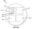
- FIG. 6Ais a top plan view of a wafer in which for solar cells are implemented.
- the depiction of four cellsis for illustration for purposes only, and the present invention is not limited to any specific number of cells per wafer.
- each cellthere are grid lines 501 (more particularly shown in cross-section in FIG. 10 ), an interconnecting bus line 502 , and a contact pad 503 .
- the geometry and number of grid and bus linesis illustrative and the present invention is not limited to the illustrated embodiment.
- FIG. 6Bis a bottom plan view of the wafer with four solar cells shown in FIG. 6A .
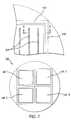
- FIG. 7is a top plan view of the wafer of FIG. 6A after the next process step in which a mesa 510 is etched around the periphery of each cell using phosphide and arsenide etchants.
- FIG. 8is a simplified cross-sectional view of the solar cell of FIG. 5B depicting just a few of the top layers and lower layers over the surrogate substrate 124 .
- FIG. 9is a cross-sectional view of the solar cell of FIG. 8 after the next process step in which the etch stop layer 104 is removed by a HCl/H 2 O solution.
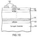
- FIG. 10is a cross-sectional view of the solar cell of FIG. 9 after the next sequence of process steps in which a photoresist mask (not shown) is placed over the contact layer 105 to form the grid lines 501 .
- the grid lines 501are deposited via evaporation and lithographically patterned and deposited over the contact layer 105 .
- the maskis lifted off to form the metal grid lines 501 .
- FIG. 11is a cross-sectional view of the solar cell of FIG. 10 after the next process step in which the grid lines are used as a mask to etch down the surface to the window layer 106 using a citric acid/peroxide etching mixture.
- FIG. 12is a cross-sectional view of the solar cell of FIG. 11 after the next process step in which an antireflective (ARC) dielectric coating layer 130 is applied over the entire surface of the “bottom” side of the wafer with the grid lines 501 .
- ARCantireflective
- FIG. 13is a cross-sectional view of the solar cell of FIG. 12 after the next process step in which the mesa 510 is etched down to the metal layer 122 using phosphide and arsenide etchants.
- the cross-section in the figureis depicted as seen from the A-A plane shown in FIG. 7 .
- One or more silver electrodesare then welded to the contact pad(s).
- FIG. 14is a cross-sectional view of the solar cell of FIG. 13 after the next process step after the surrogate substrate 124 and adhesive 123 are removed by EKC 922 .
- the preferred perforations provided in the surrogate substratehave a diameter of 0.033 inches, and are separated by 0.152 inches.
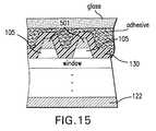
- FIG. 15is a cross-sectional view of the solar cell of FIG. 14 In one embodiment after the next process step in which an adhesive is applied over the ARC layer 130 and a rigid coverglass attached thereto.
- the solar cell of FIG. 13may be initially mounted on a support, and the surrogate substrate 124 and adhesive 123 subsequently removed.
- a supportmay be the rigid coverglass mounted by an adhesive, as depicted in FIG. 15 .
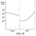
- FIG. 16is a graph of the doping profile between the emitter and base layer in a subcell of a metamorphic solar cell according to the present invention in a first embodiment.
- the doping profile of the emitter and base layers depicted in FIG. 16may be implemented in any one or more of the subcells of the triple junction solar cell of the present invention.
- the emitter dopingdecreases from approximately 5 ⁇ 10 18 per cubic centimeter in the region immediately adjacent the adjoining layer (e.g. layers 106 , 111 , or 117 ) to 5 ⁇ 10 17 per cubic centimeter in the region adjacent the p-n junction shown by the dotted line in FIG. 16 .
- the base dopingincreases exponentially from 1 ⁇ 10 16 per cubic centimeter adjacent the p-n junction to 1 ⁇ 10 18 per cubic centimeter adjacent the adjoining layer (e.g., layer 109 , 114 , or 120 ).
- the exponential doping profile taught by the present inventionproduces a constant field in the doped region.
- the bottom cellhas the smallest short circuit current among all the subcells.
- the individual subcellsare stacked and form a series circuit.
- the total current flow in the entire cellis therefore limited by the smallest current produced in any one of the subcells.
- the implementation of the present inventionwould increase efficiency by a factor of 1.067, i.e. to 32.01%.
- Such an increase in overall efficiencyis substantial in the field of solar cell technology.
- the collection field created by the exponential doping profilewill enhance the radiation hardness of the solar cell, which is important for spacecraft applications.
- the exponentially doped profileis the doping design which has been implemented and verified, other doping profiles may give rise to a linear varying collection field which may offer yet other advantages.
- a doping profile of e ⁇ x 2 / ⁇ 2produces a linear field in the doped region which would be advantageous for both minority carrier collection and for radiation hardness at the end-of-life of the solar cell.
- Such other doping profiles in one or more base layerare within the scope of the present invention.
Landscapes
- Photovoltaic Devices (AREA)
Abstract
Description
Claims (16)
Priority Applications (1)
| Application Number | Priority Date | Filing Date | Title |
|---|---|---|---|
| US12/187,454US7727795B2 (en) | 2007-12-13 | 2008-08-07 | Exponentially doped layers in inverted metamorphic multijunction solar cells |
Applications Claiming Priority (2)
| Application Number | Priority Date | Filing Date | Title |
|---|---|---|---|
| US11/956,069US20090155952A1 (en) | 2007-12-13 | 2007-12-13 | Exponentially Doped Layers In Inverted Metamorphic Multijunction Solar Cells |
| US12/187,454US7727795B2 (en) | 2007-12-13 | 2008-08-07 | Exponentially doped layers in inverted metamorphic multijunction solar cells |
Related Parent Applications (1)
| Application Number | Title | Priority Date | Filing Date |
|---|---|---|---|
| US11/956,069DivisionUS20090155952A1 (en) | 2007-12-13 | 2007-12-13 | Exponentially Doped Layers In Inverted Metamorphic Multijunction Solar Cells |
Publications (2)
| Publication Number | Publication Date |
|---|---|
| US20090155951A1 US20090155951A1 (en) | 2009-06-18 |
| US7727795B2true US7727795B2 (en) | 2010-06-01 |
Family
ID=40622227
Family Applications (2)
| Application Number | Title | Priority Date | Filing Date |
|---|---|---|---|
| US11/956,069AbandonedUS20090155952A1 (en) | 2007-12-13 | 2007-12-13 | Exponentially Doped Layers In Inverted Metamorphic Multijunction Solar Cells |
| US12/187,454ActiveUS7727795B2 (en) | 2007-12-13 | 2008-08-07 | Exponentially doped layers in inverted metamorphic multijunction solar cells |
Family Applications Before (1)
| Application Number | Title | Priority Date | Filing Date |
|---|---|---|---|
| US11/956,069AbandonedUS20090155952A1 (en) | 2007-12-13 | 2007-12-13 | Exponentially Doped Layers In Inverted Metamorphic Multijunction Solar Cells |
Country Status (5)
| Country | Link |
|---|---|
| US (2) | US20090155952A1 (en) |
| EP (1) | EP2073276B8 (en) |
| JP (2) | JP5318522B2 (en) |
| CN (1) | CN101459204A (en) |
| TW (1) | TWI355091B (en) |
Cited By (63)
| Publication number | Priority date | Publication date | Assignee | Title |
|---|---|---|---|---|
| US20090078309A1 (en)* | 2007-09-24 | 2009-03-26 | Emcore Corporation | Barrier Layers In Inverted Metamorphic Multijunction Solar Cells |
| US20090078310A1 (en)* | 2007-09-24 | 2009-03-26 | Emcore Corporation | Heterojunction Subcells In Inverted Metamorphic Multijunction Solar Cells |
| US20090272430A1 (en)* | 2008-04-30 | 2009-11-05 | Emcore Solar Power, Inc. | Refractive Index Matching in Inverted Metamorphic Multijunction Solar Cells |
| US20090272438A1 (en)* | 2008-05-05 | 2009-11-05 | Emcore Corporation | Strain Balanced Multiple Quantum Well Subcell In Inverted Metamorphic Multijunction Solar Cell |
| US20100012174A1 (en)* | 2008-07-16 | 2010-01-21 | Emcore Corporation | High band gap contact layer in inverted metamorphic multijunction solar cells |
| US20100012175A1 (en)* | 2008-07-16 | 2010-01-21 | Emcore Solar Power, Inc. | Ohmic n-contact formed at low temperature in inverted metamorphic multijunction solar cells |
| US20100031994A1 (en)* | 2008-08-07 | 2010-02-11 | Emcore Corporation | Wafer Level Interconnection of Inverted Metamorphic Multijunction Solar Cells |
| US20100093127A1 (en)* | 2006-12-27 | 2010-04-15 | Emcore Solar Power, Inc. | Inverted Metamorphic Multijunction Solar Cell Mounted on Metallized Flexible Film |
| US20100116327A1 (en)* | 2008-11-10 | 2010-05-13 | Emcore Corporation | Four junction inverted metamorphic multijunction solar cell |
| US20100122764A1 (en)* | 2008-11-14 | 2010-05-20 | Emcore Solar Power, Inc. | Surrogate Substrates for Inverted Metamorphic Multijunction Solar Cells |
| US20100122724A1 (en)* | 2008-11-14 | 2010-05-20 | Emcore Solar Power, Inc. | Four Junction Inverted Metamorphic Multijunction Solar Cell with Two Metamorphic Layers |
| US20100203730A1 (en)* | 2009-02-09 | 2010-08-12 | Emcore Solar Power, Inc. | Epitaxial Lift Off in Inverted Metamorphic Multijunction Solar Cells |
| US20100206365A1 (en)* | 2009-02-19 | 2010-08-19 | Emcore Solar Power, Inc. | Inverted Metamorphic Multijunction Solar Cells on Low Density Carriers |
| US20100229933A1 (en)* | 2009-03-10 | 2010-09-16 | Emcore Solar Power, Inc. | Inverted Metamorphic Multijunction Solar Cells with a Supporting Coating |
| US20100233838A1 (en)* | 2009-03-10 | 2010-09-16 | Emcore Solar Power, Inc. | Mounting of Solar Cells on a Flexible Substrate |
| US20100233839A1 (en)* | 2009-01-29 | 2010-09-16 | Emcore Solar Power, Inc. | String Interconnection and Fabrication of Inverted Metamorphic Multijunction Solar Cells |
| US20100229926A1 (en)* | 2009-03-10 | 2010-09-16 | Emcore Solar Power, Inc. | Four Junction Inverted Metamorphic Multijunction Solar Cell with a Single Metamorphic Layer |
| US20100282288A1 (en)* | 2009-05-06 | 2010-11-11 | Emcore Solar Power, Inc. | Solar Cell Interconnection on a Flexible Substrate |
| US20100319764A1 (en)* | 2009-06-23 | 2010-12-23 | Solar Junction Corp. | Functional Integration Of Dilute Nitrides Into High Efficiency III-V Solar Cells |
| US20110030774A1 (en)* | 2009-08-07 | 2011-02-10 | Emcore Solar Power, Inc. | Inverted Metamorphic Multijunction Solar Cells with Back Contacts |
| US20110114163A1 (en)* | 2009-11-18 | 2011-05-19 | Solar Junction Corporation | Multijunction solar cells formed on n-doped substrates |
| US8187907B1 (en) | 2010-05-07 | 2012-05-29 | Emcore Solar Power, Inc. | Solder structures for fabrication of inverted metamorphic multijunction solar cells |
| DE202012104415U1 (en) | 2011-11-15 | 2013-02-18 | Solar Junction Corp. | Multi-junction solar cells of high efficiency |
| US8507787B2 (en) | 2010-10-04 | 2013-08-13 | Samsung Electronics Co., Ltd. | Solar cell having a discontinuously graded doping concentration |
| US8575473B2 (en) | 2010-03-29 | 2013-11-05 | Solar Junction Corporation | Lattice matchable alloy for solar cells |
| US8766087B2 (en) | 2011-05-10 | 2014-07-01 | Solar Junction Corporation | Window structure for solar cell |
| US8778199B2 (en) | 2009-02-09 | 2014-07-15 | Emoore Solar Power, Inc. | Epitaxial lift off in inverted metamorphic multijunction solar cells |
| US8859892B2 (en) | 2011-02-03 | 2014-10-14 | Solar Junction Corporation | Integrated semiconductor solar cell package |
| US8895342B2 (en) | 2007-09-24 | 2014-11-25 | Emcore Solar Power, Inc. | Heterojunction subcells in inverted metamorphic multijunction solar cells |
| US8962991B2 (en) | 2011-02-25 | 2015-02-24 | Solar Junction Corporation | Pseudomorphic window layer for multijunction solar cells |
| US8962989B2 (en) | 2011-02-03 | 2015-02-24 | Solar Junction Corporation | Flexible hermetic semiconductor solar cell package with non-hermetic option |
| US9018521B1 (en) | 2008-12-17 | 2015-04-28 | Solaero Technologies Corp. | Inverted metamorphic multijunction solar cell with DBR layer adjacent to the top subcell |
| US9018519B1 (en) | 2009-03-10 | 2015-04-28 | Solaero Technologies Corp. | Inverted metamorphic multijunction solar cells having a permanent supporting substrate |
| US9117966B2 (en) | 2007-09-24 | 2015-08-25 | Solaero Technologies Corp. | Inverted metamorphic multijunction solar cell with two metamorphic layers and homojunction top cell |
| US9142615B2 (en) | 2012-10-10 | 2015-09-22 | Solar Junction Corporation | Methods and apparatus for identifying and reducing semiconductor failures |
| US9153724B2 (en) | 2012-04-09 | 2015-10-06 | Solar Junction Corporation | Reverse heterojunctions for solar cells |
| US9214594B2 (en) | 2013-08-07 | 2015-12-15 | Solaero Technologies Corp. | Fabrication of solar cells with electrically conductive polyimide adhesive |
| US9214580B2 (en) | 2010-10-28 | 2015-12-15 | Solar Junction Corporation | Multi-junction solar cell with dilute nitride sub-cell having graded doping |
| US9214586B2 (en) | 2010-04-30 | 2015-12-15 | Solar Junction Corporation | Semiconductor solar cell package |
| US9263611B2 (en) | 2011-11-17 | 2016-02-16 | Solar Junction Corporation | Method for etching multi-layer epitaxial material |
| US9287438B1 (en) | 2008-07-16 | 2016-03-15 | Solaero Technologies Corp. | Method for forming ohmic N-contacts at low temperature in inverted metamorphic multijunction solar cells with contaminant isolation |
| US9337360B1 (en) | 2009-11-16 | 2016-05-10 | Solar Junction Corporation | Non-alloyed contacts for III-V based solar cells |
| US9634172B1 (en) | 2007-09-24 | 2017-04-25 | Solaero Technologies Corp. | Inverted metamorphic multijunction solar cell with multiple metamorphic layers |
| US9680035B1 (en) | 2016-05-27 | 2017-06-13 | Solar Junction Corporation | Surface mount solar cell with integrated coverglass |
| US9758261B1 (en) | 2015-01-15 | 2017-09-12 | Solaero Technologies Corp. | Inverted metamorphic multijunction solar cell with lightweight laminate substrate |
| US9768326B1 (en) | 2013-08-07 | 2017-09-19 | Solaero Technologies Corp. | Fabrication of solar cells with electrically conductive polyimide adhesive |
| WO2017205100A1 (en) | 2016-05-23 | 2017-11-30 | Solar Junction Corporation | Exponential doping in lattice-matched dilute nitride photovoltaic cells |
| US9929300B2 (en) | 2015-11-13 | 2018-03-27 | Solaero Technologies Corp. | Multijunction solar cells with electrically conductive polyimide adhesive |
| US9935209B2 (en)* | 2016-01-28 | 2018-04-03 | Solaero Technologies Corp. | Multijunction metamorphic solar cell for space applications |
| US9934967B2 (en)* | 2008-09-19 | 2018-04-03 | Taiwan Semiconductor Manufacturing Co., Ltd. | Formation of devices by epitaxial layer overgrowth |
| US9985161B2 (en)* | 2016-08-26 | 2018-05-29 | Solaero Technologies Corp. | Multijunction metamorphic solar cell for space applications |
| US10090420B2 (en) | 2016-01-22 | 2018-10-02 | Solar Junction Corporation | Via etch method for back contact multijunction solar cells |
| US10153388B1 (en) | 2013-03-15 | 2018-12-11 | Solaero Technologies Corp. | Emissivity coating for space solar cell arrays |
| US10170656B2 (en) | 2009-03-10 | 2019-01-01 | Solaero Technologies Corp. | Inverted metamorphic multijunction solar cell with a single metamorphic layer |
| US10381501B2 (en) | 2006-06-02 | 2019-08-13 | Solaero Technologies Corp. | Inverted metamorphic multijunction solar cell with multiple metamorphic layers |
| US10381505B2 (en) | 2007-09-24 | 2019-08-13 | Solaero Technologies Corp. | Inverted metamorphic multijunction solar cells including metamorphic layers |
| US10541349B1 (en) | 2008-12-17 | 2020-01-21 | Solaero Technologies Corp. | Methods of forming inverted multijunction solar cells with distributed Bragg reflector |
| US10916675B2 (en) | 2015-10-19 | 2021-02-09 | Array Photonics, Inc. | High efficiency multijunction photovoltaic cells |
| US10930808B2 (en) | 2017-07-06 | 2021-02-23 | Array Photonics, Inc. | Hybrid MOCVD/MBE epitaxial growth of high-efficiency lattice-matched multijunction solar cells |
| US11011660B1 (en) | 2018-07-17 | 2021-05-18 | Solaero Technologies Corp. | Inverted metamorphic multijunction solar cell |
| US11211514B2 (en) | 2019-03-11 | 2021-12-28 | Array Photonics, Inc. | Short wavelength infrared optoelectronic devices having graded or stepped dilute nitride active regions |
| US11233166B2 (en) | 2014-02-05 | 2022-01-25 | Array Photonics, Inc. | Monolithic multijunction power converter |
| US11271122B2 (en) | 2017-09-27 | 2022-03-08 | Array Photonics, Inc. | Short wavelength infrared optoelectronic devices having a dilute nitride layer |
Families Citing this family (39)
| Publication number | Priority date | Publication date | Assignee | Title |
|---|---|---|---|---|
| US20100229913A1 (en)* | 2009-01-29 | 2010-09-16 | Emcore Solar Power, Inc. | Contact Layout and String Interconnection of Inverted Metamorphic Multijunction Solar Cells |
| US20100047959A1 (en)* | 2006-08-07 | 2010-02-25 | Emcore Solar Power, Inc. | Epitaxial Lift Off on Film Mounted Inverted Metamorphic Multijunction Solar Cells |
| US20110041898A1 (en)* | 2009-08-19 | 2011-02-24 | Emcore Solar Power, Inc. | Back Metal Layers in Inverted Metamorphic Multijunction Solar Cells |
| US7741146B2 (en) | 2008-08-12 | 2010-06-22 | Emcore Solar Power, Inc. | Demounting of inverted metamorphic multijunction solar cells |
| US20100282305A1 (en) | 2009-05-08 | 2010-11-11 | Emcore Solar Power, Inc. | Inverted Multijunction Solar Cells with Group IV/III-V Hybrid Alloys |
| IT1394853B1 (en)* | 2009-07-21 | 2012-07-20 | Cesi Ct Elettrotecnico Sperimentale Italiano Giacinto Motta S P A | PHOTOVOLTAIC CELL WITH HIGH CONVERSION EFFICIENCY |
| US8961687B2 (en)* | 2009-08-31 | 2015-02-24 | Alliance For Sustainable Energy, Llc | Lattice matched crystalline substrates for cubic nitride semiconductor growth |
| US8575471B2 (en)* | 2009-08-31 | 2013-11-05 | Alliance For Sustainable Energy, Llc | Lattice matched semiconductor growth on crystalline metallic substrates |
| DE102009049397B4 (en) | 2009-10-14 | 2018-09-06 | Solaero Technologies Corp. | Production method with surrogate substrate for inverted metamorphic multi-junction solar cells |
| DE102009057020B4 (en)* | 2009-12-03 | 2021-04-29 | Solaero Technologies Corp. | Growth substrates for inverted metamorphic multijunction solar cells |
| US8507365B2 (en)* | 2009-12-21 | 2013-08-13 | Alliance For Sustainable Energy, Llc | Growth of coincident site lattice matched semiconductor layers and devices on crystalline substrates |
| TWI414073B (en)* | 2010-07-20 | 2013-11-01 | Cesi Ct Elettrotecnico Sperimentale Italiano Giacinto Motta S P A | Photovoltaic cell having a high conversion efficiency |
| TWI427807B (en)* | 2010-10-28 | 2014-02-21 | Atomic Energy Council | A solar cell structure with improved collection efficiency of photocurrent |
| WO2012074523A1 (en) | 2010-12-01 | 2012-06-07 | Alliance For Sustainable Energy, Llc | Methods of producing free-standing semiconductors using sacrificial buffer layers and recyclable substrates |
| US9425249B2 (en) | 2010-12-01 | 2016-08-23 | Alliance For Sustainable Energy, Llc | Coincident site lattice-matched growth of semiconductors on substrates using compliant buffer layers |
| CN102244114A (en)* | 2011-06-22 | 2011-11-16 | 厦门市三安光电科技有限公司 | High-concentration multi-junction solar cell and preparation method thereof |
| JP5758257B2 (en)* | 2011-09-30 | 2015-08-05 | シャープ株式会社 | Laminate for producing compound semiconductor solar cell, compound semiconductor solar cell and method for producing the same |
| CN102651417B (en)* | 2012-05-18 | 2014-09-03 | 中国科学院苏州纳米技术与纳米仿生研究所 | Three-knot cascading solar battery and preparation method thereof |
| CN102779890A (en)* | 2012-08-14 | 2012-11-14 | 厦门乾照光电股份有限公司 | Inverted triple-junction solar cell and method for manufacturing same |
| US20170062642A1 (en)* | 2013-04-29 | 2017-03-02 | Solaero Technologies Corp. | Inverted metamorphic multijunction solar cell |
| US9853180B2 (en) | 2013-06-19 | 2017-12-26 | Solaero Technologies Corp. | Inverted metamorphic multijunction solar cell with surface passivation |
| ITMI20131297A1 (en)* | 2013-08-01 | 2015-02-02 | Cesi Ct Elettrotecnico Sperim Entale Italian | PHOTOVOLTAIC CELL WITH VARIABLE PROHIBITED BAND |
| US10270000B2 (en)* | 2015-10-19 | 2019-04-23 | Solaero Technologies Corp. | Multijunction metamorphic solar cell assembly for space applications |
| US10256359B2 (en) | 2015-10-19 | 2019-04-09 | Solaero Technologies Corp. | Lattice matched multijunction solar cell assemblies for space applications |
| US10361330B2 (en) | 2015-10-19 | 2019-07-23 | Solaero Technologies Corp. | Multijunction solar cell assemblies for space applications |
| US10403778B2 (en) | 2015-10-19 | 2019-09-03 | Solaero Technologies Corp. | Multijunction solar cell assembly for space applications |
| CN105304764B (en)* | 2015-11-11 | 2017-12-05 | 厦门乾照光电股份有限公司 | A kind of inverted structure method for manufacturing solar battery |
| CN106784127B (en)* | 2015-11-20 | 2019-02-01 | 北京创昱科技有限公司 | A kind of binode Thinfilm solar cell assembly and preparation method thereof |
| CN106784108B (en)* | 2015-11-20 | 2019-05-31 | 北京创昱科技有限公司 | A kind of binode Thinfilm solar cell assembly and preparation method thereof |
| US11316053B2 (en)* | 2016-08-26 | 2022-04-26 | Sol Aero Technologies Corp. | Multijunction solar cell assembly |
| US10263134B1 (en) | 2016-05-25 | 2019-04-16 | Solaero Technologies Corp. | Multijunction solar cells having an indirect high band gap semiconductor emitter layer in the upper solar subcell |
| US12249667B2 (en) | 2017-08-18 | 2025-03-11 | Solaero Technologies Corp. | Space vehicles including multijunction metamorphic solar cells |
| US10700230B1 (en)* | 2016-10-14 | 2020-06-30 | Solaero Technologies Corp. | Multijunction metamorphic solar cell for space applications |
| US10636926B1 (en) | 2016-12-12 | 2020-04-28 | Solaero Technologies Corp. | Distributed BRAGG reflector structures in multijunction solar cells |
| KR101931712B1 (en)* | 2016-12-28 | 2018-12-24 | 엘지전자 주식회사 | Compound semiconductor solar cell |
| US20190181289A1 (en) | 2017-12-11 | 2019-06-13 | Solaero Technologies Corp. | Multijunction solar cells |
| WO2020247691A1 (en)* | 2019-06-04 | 2020-12-10 | Solar Junction Corporation | Dilute nitride optical absorption layers having graded doping |
| US12046693B2 (en)* | 2021-09-01 | 2024-07-23 | Maxeon Solar Pte. Ltd. | Solar device fabrication limiting power conversion losses |
| CN114335208B (en)* | 2022-03-16 | 2022-06-10 | 南昌凯迅光电股份有限公司 | Novel gallium arsenide solar cell and manufacturing method thereof |
Citations (37)
| Publication number | Priority date | Publication date | Assignee | Title |
|---|---|---|---|---|
| US4001864A (en) | 1976-01-30 | 1977-01-04 | Gibbons James F | Semiconductor p-n junction solar cell and method of manufacture |
| US4255211A (en) | 1979-12-31 | 1981-03-10 | Chevron Research Company | Multilayer photovoltaic solar cell with semiconductor layer at shorting junction interface |
| US4338480A (en) | 1980-12-29 | 1982-07-06 | Varian Associates, Inc. | Stacked multijunction photovoltaic converters |
| US4612408A (en) | 1984-10-22 | 1986-09-16 | Sera Solar Corporation | Electrically isolated semiconductor integrated photodiode circuits and method |
| US4881979A (en) | 1984-08-29 | 1989-11-21 | Varian Associates, Inc. | Junctions for monolithic cascade solar cells and methods |
| US5019177A (en) | 1989-11-03 | 1991-05-28 | The United States Of America As Represented By The United States Department Of Energy | Monolithic tandem solar cell |
| US5021360A (en) | 1989-09-25 | 1991-06-04 | Gte Laboratories Incorporated | Method of farbicating highly lattice mismatched quantum well structures |
| US5053083A (en) | 1989-05-08 | 1991-10-01 | The Board Of Trustees Of The Leland Stanford Junior University | Bilevel contact solar cells |
| US5217539A (en) | 1991-09-05 | 1993-06-08 | The Boeing Company | III-V solar cells and doping processes |
| US5322572A (en) | 1989-11-03 | 1994-06-21 | The United States Of America As Represented By The United States Department Of Energy | Monolithic tandem solar cell |
| US5342453A (en) | 1992-11-13 | 1994-08-30 | Midwest Research Institute | Heterojunction solar cell |
| US5376185A (en) | 1993-05-12 | 1994-12-27 | Midwest Research Institute | Single-junction solar cells with the optimum band gap for terrestrial concentrator applications |
| US5479032A (en) | 1994-07-21 | 1995-12-26 | Trustees Of Princeton University | Multiwavelength infrared focal plane array detector |
| US5944913A (en) | 1997-11-26 | 1999-08-31 | Sandia Corporation | High-efficiency solar cell and method for fabrication |
| US6180432B1 (en) | 1998-03-03 | 2001-01-30 | Interface Studies, Inc. | Fabrication of single absorber layer radiated energy conversion device |
| US6239354B1 (en) | 1998-10-09 | 2001-05-29 | Midwest Research Institute | Electrical isolation of component cells in monolithically interconnected modules |
| US6252287B1 (en) | 1999-05-19 | 2001-06-26 | Sandia Corporation | InGaAsN/GaAs heterojunction for multi-junction solar cells |
| US6281426B1 (en) | 1997-10-01 | 2001-08-28 | Midwest Research Institute | Multi-junction, monolithic solar cell using low-band-gap materials lattice matched to GaAs or Ge |
| US6300558B1 (en) | 1999-04-27 | 2001-10-09 | Japan Energy Corporation | Lattice matched solar cell and method for manufacturing the same |
| US6300557B1 (en) | 1998-10-09 | 2001-10-09 | Midwest Research Institute | Low-bandgap double-heterostructure InAsP/GaInAs photovoltaic converters |
| US6340788B1 (en) | 1999-12-02 | 2002-01-22 | Hughes Electronics Corporation | Multijunction photovoltaic cells and panels using a silicon or silicon-germanium active substrate cell for space and terrestrial applications |
| US20020117675A1 (en) | 2001-02-09 | 2002-08-29 | Angelo Mascarenhas | Isoelectronic co-doping |
| US6482672B1 (en) | 1997-11-06 | 2002-11-19 | Essential Research, Inc. | Using a critical composition grading technique to deposit InGaAs epitaxial layers on InP substrates |
| US6660928B1 (en) | 2002-04-02 | 2003-12-09 | Essential Research, Inc. | Multi-junction photovoltaic cell |
| US20040200523A1 (en) | 2003-04-14 | 2004-10-14 | The Boeing Company | Multijunction photovoltaic cell grown on high-miscut-angle substrate |
| WO2005015638A1 (en) | 2003-07-22 | 2005-02-17 | Akzo Nobel N.V. | Process for manufacturing a solar cell foil using a temporary substrate |
| US6951819B2 (en) | 2002-12-05 | 2005-10-04 | Blue Photonics, Inc. | High efficiency, monolithic multijunction solar cells containing lattice-mismatched materials and methods of forming same |
| US20060021565A1 (en) | 2004-07-30 | 2006-02-02 | Aonex Technologies, Inc. | GaInP / GaAs / Si triple junction solar cell enabled by wafer bonding and layer transfer |
| FR2878076A1 (en) | 2004-11-17 | 2006-05-19 | St Microelectronics Sa | SLIMMING A SEMICONDUCTOR WAFER |
| US7071407B2 (en) | 2002-10-31 | 2006-07-04 | Emcore Corporation | Method and apparatus of multiplejunction solar cell structure with high band gap heterojunction middle cell |
| US20060144435A1 (en)* | 2002-05-21 | 2006-07-06 | Wanlass Mark W | High-efficiency, monolithic, multi-bandgap, tandem photovoltaic energy converters |
| US20060162768A1 (en) | 2002-05-21 | 2006-07-27 | Wanlass Mark W | Low bandgap, monolithic, multi-bandgap, optoelectronic devices |
| US20070272946A1 (en) | 2006-04-04 | 2007-11-29 | Francois Pagette | Silicon germanium emitter |
| US20070277873A1 (en)* | 2006-06-02 | 2007-12-06 | Emcore Corporation | Metamorphic layers in multijunction solar cells |
| US20080185038A1 (en) | 2007-02-02 | 2008-08-07 | Emcore Corporation | Inverted metamorphic solar cell with via for backside contacts |
| US20080245409A1 (en) | 2006-12-27 | 2008-10-09 | Emcore Corporation | Inverted Metamorphic Solar Cell Mounted on Flexible Film |
| EP0658944B1 (en) | 1993-12-14 | 2009-04-15 | Spectrolab, Inc. | Thin semiconductor device and method of fabrication |
Family Cites Families (50)
| Publication number | Priority date | Publication date | Assignee | Title |
|---|---|---|---|---|
| US3488834A (en)* | 1965-10-20 | 1970-01-13 | Texas Instruments Inc | Microelectronic circuit formed in an insulating substrate and method of making same |
| US3964155A (en)* | 1972-02-23 | 1976-06-22 | The United States Of America As Represented By The Secretary Of The Navy | Method of planar mounting of silicon solar cells |
| DE3036260A1 (en)* | 1980-09-26 | 1982-04-29 | Licentia Patent-Verwaltungs-Gmbh, 6000 Frankfurt | METHOD FOR PRODUCING ELECTRICAL CONTACTS ON A SILICON SOLAR CELL |
| JPH065765B2 (en)* | 1982-12-23 | 1994-01-19 | 株式会社半導体エネルギ−研究所 | Photoelectric conversion device |
| JPS63244887A (en)* | 1987-03-31 | 1988-10-12 | Sharp Corp | amorphous solar cell |
| JPH0472773A (en)* | 1990-07-13 | 1992-03-06 | Hitachi Cable Ltd | Multilayer junction solar cell |
| JP3169497B2 (en)* | 1993-12-24 | 2001-05-28 | 三菱電機株式会社 | Solar cell manufacturing method |
| US6165873A (en)* | 1998-11-27 | 2000-12-26 | Nec Corporation | Process for manufacturing a semiconductor integrated circuit device |
| US20030070707A1 (en)* | 2001-10-12 | 2003-04-17 | King Richard Roland | Wide-bandgap, lattice-mismatched window layer for a solar energy conversion device |
| US6690041B2 (en)* | 2002-05-14 | 2004-02-10 | Global Solar Energy, Inc. | Monolithically integrated diodes in thin-film photovoltaic devices |
| US6794631B2 (en)* | 2002-06-07 | 2004-09-21 | Corning Lasertron, Inc. | Three-terminal avalanche photodiode |
| US7122734B2 (en)* | 2002-10-23 | 2006-10-17 | The Boeing Company | Isoelectronic surfactant suppression of threading dislocations in metamorphic epitaxial layers |
| US20050211291A1 (en)* | 2004-03-23 | 2005-09-29 | The Boeing Company | Solar cell assembly |
| US8227689B2 (en)* | 2004-06-15 | 2012-07-24 | The Boeing Company | Solar cells having a transparent composition-graded buffer layer |
| US7846759B2 (en)* | 2004-10-21 | 2010-12-07 | Aonex Technologies, Inc. | Multi-junction solar cells and methods of making same using layer transfer and bonding techniques |
| US7166520B1 (en)* | 2005-08-08 | 2007-01-23 | Silicon Genesis Corporation | Thin handle substrate method and structure for fabricating devices using one or more films provided by a layer transfer process |
| US8637759B2 (en)* | 2005-12-16 | 2014-01-28 | The Boeing Company | Notch filter for triple junction solar cells |
| US20100122724A1 (en)* | 2008-11-14 | 2010-05-20 | Emcore Solar Power, Inc. | Four Junction Inverted Metamorphic Multijunction Solar Cell with Two Metamorphic Layers |
| US20090078309A1 (en)* | 2007-09-24 | 2009-03-26 | Emcore Corporation | Barrier Layers In Inverted Metamorphic Multijunction Solar Cells |
| US20100229926A1 (en)* | 2009-03-10 | 2010-09-16 | Emcore Solar Power, Inc. | Four Junction Inverted Metamorphic Multijunction Solar Cell with a Single Metamorphic Layer |
| US20100186804A1 (en)* | 2009-01-29 | 2010-07-29 | Emcore Solar Power, Inc. | String Interconnection of Inverted Metamorphic Multijunction Solar Cells on Flexible Perforated Carriers |
| US20090078308A1 (en)* | 2007-09-24 | 2009-03-26 | Emcore Corporation | Thin Inverted Metamorphic Multijunction Solar Cells with Rigid Support |
| US20090078310A1 (en)* | 2007-09-24 | 2009-03-26 | Emcore Corporation | Heterojunction Subcells In Inverted Metamorphic Multijunction Solar Cells |
| US20100229913A1 (en)* | 2009-01-29 | 2010-09-16 | Emcore Solar Power, Inc. | Contact Layout and String Interconnection of Inverted Metamorphic Multijunction Solar Cells |
| US20100047959A1 (en)* | 2006-08-07 | 2010-02-25 | Emcore Solar Power, Inc. | Epitaxial Lift Off on Film Mounted Inverted Metamorphic Multijunction Solar Cells |
| US20080029151A1 (en)* | 2006-08-07 | 2008-02-07 | Mcglynn Daniel | Terrestrial solar power system using III-V semiconductor solar cells |
| US20100203730A1 (en)* | 2009-02-09 | 2010-08-12 | Emcore Solar Power, Inc. | Epitaxial Lift Off in Inverted Metamorphic Multijunction Solar Cells |
| US20080149173A1 (en)* | 2006-12-21 | 2008-06-26 | Sharps Paul R | Inverted metamorphic solar cell with bypass diode |
| US20110041898A1 (en)* | 2009-08-19 | 2011-02-24 | Emcore Solar Power, Inc. | Back Metal Layers in Inverted Metamorphic Multijunction Solar Cells |
| US20090038679A1 (en)* | 2007-08-09 | 2009-02-12 | Emcore Corporation | Thin Multijunction Solar Cells With Plated Metal OHMIC Contact and Support |
| US20090078311A1 (en)* | 2007-09-24 | 2009-03-26 | Emcore Corporation | Surfactant Assisted Growth in Barrier Layers In Inverted Metamorphic Multijunction Solar Cells |
| US20100233838A1 (en)* | 2009-03-10 | 2010-09-16 | Emcore Solar Power, Inc. | Mounting of Solar Cells on a Flexible Substrate |
| US20090223554A1 (en)* | 2008-03-05 | 2009-09-10 | Emcore Corporation | Dual Sided Photovoltaic Package |
| US20090229658A1 (en)* | 2008-03-13 | 2009-09-17 | Emcore Corporation | Non-Isoelectronic Surfactant Assisted Growth In Inverted Metamorphic Multijunction Solar Cells |
| US20090229662A1 (en)* | 2008-03-13 | 2009-09-17 | Emcore Corporation | Off-Cut Substrates In Inverted Metamorphic Multijunction Solar Cells |
| US20090272430A1 (en)* | 2008-04-30 | 2009-11-05 | Emcore Solar Power, Inc. | Refractive Index Matching in Inverted Metamorphic Multijunction Solar Cells |
| US20100012175A1 (en)* | 2008-07-16 | 2010-01-21 | Emcore Solar Power, Inc. | Ohmic n-contact formed at low temperature in inverted metamorphic multijunction solar cells |
| US20090272438A1 (en)* | 2008-05-05 | 2009-11-05 | Emcore Corporation | Strain Balanced Multiple Quantum Well Subcell In Inverted Metamorphic Multijunction Solar Cell |
| US20090288703A1 (en)* | 2008-05-20 | 2009-11-26 | Emcore Corporation | Wide Band Gap Window Layers In Inverted Metamorphic Multijunction Solar Cells |
| US20100012174A1 (en)* | 2008-07-16 | 2010-01-21 | Emcore Corporation | High band gap contact layer in inverted metamorphic multijunction solar cells |
| US8263853B2 (en)* | 2008-08-07 | 2012-09-11 | Emcore Solar Power, Inc. | Wafer level interconnection of inverted metamorphic multijunction solar cells |
| US7741146B2 (en)* | 2008-08-12 | 2010-06-22 | Emcore Solar Power, Inc. | Demounting of inverted metamorphic multijunction solar cells |
| US8236600B2 (en)* | 2008-11-10 | 2012-08-07 | Emcore Solar Power, Inc. | Joining method for preparing an inverted metamorphic multijunction solar cell |
| US20100122764A1 (en)* | 2008-11-14 | 2010-05-20 | Emcore Solar Power, Inc. | Surrogate Substrates for Inverted Metamorphic Multijunction Solar Cells |
| US20100147366A1 (en)* | 2008-12-17 | 2010-06-17 | Emcore Solar Power, Inc. | Inverted Metamorphic Multijunction Solar Cells with Distributed Bragg Reflector |
| US7960201B2 (en)* | 2009-01-29 | 2011-06-14 | Emcore Solar Power, Inc. | String interconnection and fabrication of inverted metamorphic multijunction solar cells |
| US20100206365A1 (en)* | 2009-02-19 | 2010-08-19 | Emcore Solar Power, Inc. | Inverted Metamorphic Multijunction Solar Cells on Low Density Carriers |
| US20100229933A1 (en)* | 2009-03-10 | 2010-09-16 | Emcore Solar Power, Inc. | Inverted Metamorphic Multijunction Solar Cells with a Supporting Coating |
| US20100282288A1 (en)* | 2009-05-06 | 2010-11-11 | Emcore Solar Power, Inc. | Solar Cell Interconnection on a Flexible Substrate |
| US8263856B2 (en)* | 2009-08-07 | 2012-09-11 | Emcore Solar Power, Inc. | Inverted metamorphic multijunction solar cells with back contacts |
- 2007
- 2007-12-13USUS11/956,069patent/US20090155952A1/ennot_activeAbandoned
- 2008
- 2008-08-07USUS12/187,454patent/US7727795B2/enactiveActive
- 2008-08-26TWTW097132608Apatent/TWI355091B/ennot_activeIP Right Cessation
- 2008-09-10CNCNA2008101495330Apatent/CN101459204A/enactivePending
- 2008-10-20JPJP2008269598Apatent/JP5318522B2/enactiveActive
- 2008-12-11EPEP08021551.0Apatent/EP2073276B8/enactiveActive
- 2013
- 2013-05-17JPJP2013105060Apatent/JP5456923B2/enactiveActive
Patent Citations (38)
| Publication number | Priority date | Publication date | Assignee | Title |
|---|---|---|---|---|
| US4001864A (en) | 1976-01-30 | 1977-01-04 | Gibbons James F | Semiconductor p-n junction solar cell and method of manufacture |
| US4255211A (en) | 1979-12-31 | 1981-03-10 | Chevron Research Company | Multilayer photovoltaic solar cell with semiconductor layer at shorting junction interface |
| US4338480A (en) | 1980-12-29 | 1982-07-06 | Varian Associates, Inc. | Stacked multijunction photovoltaic converters |
| US4881979A (en) | 1984-08-29 | 1989-11-21 | Varian Associates, Inc. | Junctions for monolithic cascade solar cells and methods |
| US4612408A (en) | 1984-10-22 | 1986-09-16 | Sera Solar Corporation | Electrically isolated semiconductor integrated photodiode circuits and method |
| US5053083A (en) | 1989-05-08 | 1991-10-01 | The Board Of Trustees Of The Leland Stanford Junior University | Bilevel contact solar cells |
| US5021360A (en) | 1989-09-25 | 1991-06-04 | Gte Laboratories Incorporated | Method of farbicating highly lattice mismatched quantum well structures |
| US5019177A (en) | 1989-11-03 | 1991-05-28 | The United States Of America As Represented By The United States Department Of Energy | Monolithic tandem solar cell |
| US5322572A (en) | 1989-11-03 | 1994-06-21 | The United States Of America As Represented By The United States Department Of Energy | Monolithic tandem solar cell |
| US5217539A (en) | 1991-09-05 | 1993-06-08 | The Boeing Company | III-V solar cells and doping processes |
| US5342453A (en) | 1992-11-13 | 1994-08-30 | Midwest Research Institute | Heterojunction solar cell |
| US5376185A (en) | 1993-05-12 | 1994-12-27 | Midwest Research Institute | Single-junction solar cells with the optimum band gap for terrestrial concentrator applications |
| EP0658944B1 (en) | 1993-12-14 | 2009-04-15 | Spectrolab, Inc. | Thin semiconductor device and method of fabrication |
| US5479032A (en) | 1994-07-21 | 1995-12-26 | Trustees Of Princeton University | Multiwavelength infrared focal plane array detector |
| US6281426B1 (en) | 1997-10-01 | 2001-08-28 | Midwest Research Institute | Multi-junction, monolithic solar cell using low-band-gap materials lattice matched to GaAs or Ge |
| US6482672B1 (en) | 1997-11-06 | 2002-11-19 | Essential Research, Inc. | Using a critical composition grading technique to deposit InGaAs epitaxial layers on InP substrates |
| US5944913A (en) | 1997-11-26 | 1999-08-31 | Sandia Corporation | High-efficiency solar cell and method for fabrication |
| US6180432B1 (en) | 1998-03-03 | 2001-01-30 | Interface Studies, Inc. | Fabrication of single absorber layer radiated energy conversion device |
| US6239354B1 (en) | 1998-10-09 | 2001-05-29 | Midwest Research Institute | Electrical isolation of component cells in monolithically interconnected modules |
| US6300557B1 (en) | 1998-10-09 | 2001-10-09 | Midwest Research Institute | Low-bandgap double-heterostructure InAsP/GaInAs photovoltaic converters |
| US6300558B1 (en) | 1999-04-27 | 2001-10-09 | Japan Energy Corporation | Lattice matched solar cell and method for manufacturing the same |
| US6252287B1 (en) | 1999-05-19 | 2001-06-26 | Sandia Corporation | InGaAsN/GaAs heterojunction for multi-junction solar cells |
| US6340788B1 (en) | 1999-12-02 | 2002-01-22 | Hughes Electronics Corporation | Multijunction photovoltaic cells and panels using a silicon or silicon-germanium active substrate cell for space and terrestrial applications |
| US20020117675A1 (en) | 2001-02-09 | 2002-08-29 | Angelo Mascarenhas | Isoelectronic co-doping |
| US6660928B1 (en) | 2002-04-02 | 2003-12-09 | Essential Research, Inc. | Multi-junction photovoltaic cell |
| US20060144435A1 (en)* | 2002-05-21 | 2006-07-06 | Wanlass Mark W | High-efficiency, monolithic, multi-bandgap, tandem photovoltaic energy converters |
| US20060162768A1 (en) | 2002-05-21 | 2006-07-27 | Wanlass Mark W | Low bandgap, monolithic, multi-bandgap, optoelectronic devices |
| US7071407B2 (en) | 2002-10-31 | 2006-07-04 | Emcore Corporation | Method and apparatus of multiplejunction solar cell structure with high band gap heterojunction middle cell |
| US6951819B2 (en) | 2002-12-05 | 2005-10-04 | Blue Photonics, Inc. | High efficiency, monolithic multijunction solar cells containing lattice-mismatched materials and methods of forming same |
| US20040200523A1 (en) | 2003-04-14 | 2004-10-14 | The Boeing Company | Multijunction photovoltaic cell grown on high-miscut-angle substrate |
| WO2005015638A1 (en) | 2003-07-22 | 2005-02-17 | Akzo Nobel N.V. | Process for manufacturing a solar cell foil using a temporary substrate |
| US20060021565A1 (en) | 2004-07-30 | 2006-02-02 | Aonex Technologies, Inc. | GaInP / GaAs / Si triple junction solar cell enabled by wafer bonding and layer transfer |
| FR2878076A1 (en) | 2004-11-17 | 2006-05-19 | St Microelectronics Sa | SLIMMING A SEMICONDUCTOR WAFER |
| US20070218649A1 (en) | 2004-11-17 | 2007-09-20 | Stmicroelectronics Sa | Semiconductor wafer thinning |
| US20070272946A1 (en) | 2006-04-04 | 2007-11-29 | Francois Pagette | Silicon germanium emitter |
| US20070277873A1 (en)* | 2006-06-02 | 2007-12-06 | Emcore Corporation | Metamorphic layers in multijunction solar cells |
| US20080245409A1 (en) | 2006-12-27 | 2008-10-09 | Emcore Corporation | Inverted Metamorphic Solar Cell Mounted on Flexible Film |
| US20080185038A1 (en) | 2007-02-02 | 2008-08-07 | Emcore Corporation | Inverted metamorphic solar cell with via for backside contacts |
Non-Patent Citations (27)
| Title |
|---|
| "Partial European Search Report," Application No. EP 08 01 3466. Feb. 12, 2009. European Patent Office, Berlin. Germany. |
| A. Cornfeld, et al., "Advances in the Performance of Inverted Metamorphic Multi-junction Solar Cells." 23rd European Photovoltaic Energy Conference, Sep. 1-5, 2008, Valencia, Spain. |
| A. Cornfeld, et al., "Development of a Large Area Inverted Metamorphic Multi-junction (IMM) Highly Efficient AM0 Solar Cell." 33rd IEEE Photovoltaic Specialists Conference, May 11-16, 2008, San Diego, CA, USA. |
| A. Cornfeld, et al., "Development of a Large Area Inverted Metamorphic Multi-junction Highly Efficient AM0 Solar Cell." Conference paper presented at the 33rd IEEE Photovoltaic Specialists Conference May 11-16, 2008 on May 12, 2008. San Diego, CA, USA. 17 pages. |
| An Inverted-Growth Approach to Development of an IR-Transparent, High-Efficiency A1GaAs/GaAs Cascade Solar Cell, R. Venkatasubramanian, et al., Research Triangel Institute, 1991 IEEE, pp. 93-98. |
| D.J. Friedman, et al., "0.7-eV GaInAs Junction for a GaInP/GaAs/GaInAs(1eV)/GaInAs(0.7eV) Four-Junction Solar Cell." 2006 IEEE 4th World Conference on Photovoltaic Energy Conversion, May 7-12, 2006, Waikoloa, Hawaii, USA. |
| Fahrenbruch, A.L., et al. Fundamentals of Solar Cells: Photovoltaic Solar Energy Conversion. pp. 280-283. 1983. Academic Press, New York, NY. |
| Green, M.A. "Do Built-in Fields Improve Solar Cell Performance?" Progress in Photovoltaics: Research and Applications. 2009, 17: 57-66. John Wiley & Sons, Inc., New York, NY. |
| H. Yoon, et al., "Progress of Inverted metamorphic III-V Solar Cell Development at Spectrolab." 33rd IEEE Photovoltaic Specialists Conference, May 11-16, 2008, San Diego, CA, USA. |
| J.F. Geisz, et al., "High-efficiency GaInP/GaAs/InGaAs triple-junction solar cells grown inverted with a metamorphic bottom junction." Applied Phyics Letters 91, 023502 (2007), pp. 023502-1-02305.3. Online publication Jul. 10, 2007. American Institute of Physics, Melville, NY, USA. |
| J.F. Geisz, et al., "Inverted GaInP / (In)GaAs / InGaAs Triple-Junction Solar Cells with Low-Stress Metamorphic Bottom Junctions." 33rd IEEE Photovoltaic Specialists Conference, May 11-16, 2008, San Diego, CA, USA. |
| Lattice-Mismatched Approaches for High-Performance, III-V Photovoltaic Energy Converters, M.W. Wanlass et al., 2005 IEEE, pp. 530-535. |
| M. Stan, et al., "Very High Efficiency Triple Junction Solar Cells by MOVPE." 14th International Conference of Metalorganic Vapor Phase Epitaxy. Jun. 1-6, 2008, Metz, France. |
| M. Yamaguchi, "Physics and Technologies of Superhigh-Efficiency Tandem Solar Cells." Semiconductors, vol. 33, No. 9, Sep. 1999, pp. 961-964. Toyota Technological Institute, Nagoya, Japan. ©1999, American Institute of Physics. |
| M.W. Wanlass et al., "Lattice-Mismatched Approached for High-Performance, III-V Photovoltaic Energy Converters." Proceedings of the 31st IEEE PVSC, Jan. 3-7, 2005, Lake Buena Vista, FL, USA. |
| M.W. Wanlass et al., "Monolithic, Ultra-Thin GaInP/GaAs/GaInAs Tandem Solar Cells." 2006 IEEE 4th World Conference on Photovoltaic Energy Conversion, May 7-12, 2006, Waikoloa, Hawaii, USA. |
| Messenger, R.A. Photovoltaic Systems Engineering. Second Edition, 2004. pp. 364-365. CRC Press, Boca Raton, FL. |
| P. Sharps, et al., "Inverting the triple junction improves efficiency and flexibility." Compound Semiconductor. Oct. 2007, pp. 25-28. IOP Publishing, Ltd., Bristol, England. |
| R. Venkatasubramanian, et al., "An Inverted-Growth Approach to Development of an IR-Transparent, High-Efficiency AlGaAs/GaAs Cascade Solar Cell." 22nd IEEE Photovoltaic Specialists Conference, Oct. 7-11, 1991, Las Vegas, NV, USA. |
| R.R. King, et al., "High-Efficiency Space and Terrestrial Multijunction Solar Cells Through Bandgap Control in Cell Structures." 2002 Photovoltaic Specialists Conference, Conference Record of the 29th IEEE, May 19-24, 2002, pp. 776-781. New Orleans, LA, USA. |
| R.R. King, et al., "Next-Generation, High-Efficiency III-V Multijunction Solar Cells." 28th IEEE Photovoltaic Specialists Conference, Sep. 15-22, 2000, Anchorage, AK, USA. |
| S. Sinharoy, et al., "Progress in the Development of Metamorphic Multi-junction III-V Space Solar Cells." Progress in Photovoltaics: Research and Applications, vol. 10, Feb. 2002, pp. 427-432. John Wiley & Sons, Ltd. Hoboken, NJ, USA. |
| Schultz, J.C., et al., "Development of High-Quantum-Efficiency, Lattice-Mismatched, 1.0-eV GaInAs Solar Cells." Journal of Electronic Materials, vol. 22, No. 7, Jul. 1993. pp. 755-761. The Minerals, Metals, & Materials Society (TMS)/IEEE. Springer New York, New York, NY. |
| Streit et al., "Effect of exponentially Graded Base Doping on the Performance of GaAs/AlGaAs Heterojunction Bipolar Transistor", IEEE Electron Device Letter, vol. 12, No. 5, May 1991.* |
| Takamoto, T., et al., "InGaP/GaAS-based Multijunction Solar Cells." Progress in Photovoltaics: Research and Application, 2005; vol. 13, pp. 495-511. Wiley InterScience, John Wiley & Sons, Ltd., Hoboken, NJ. |
| Wolf, M. "Drift Fields in Photovoltaic Solar Energy Converter Cells." Proceedings of the IEEE, vol. 51, No. 5, 1963. pp. 674-693. IEEE, Piscataway, NJ. |
| Würfel, P. Physics of Solar Cells: from Basic Principles to Advanced Concepts. 2nd updated and expanded edition, 2009. ISBN 978-3-527-40857-6. Sections 6.4 and 6.8 17 pages. Wiley-VCH: Weinheim, Germany. |
Cited By (90)
| Publication number | Priority date | Publication date | Assignee | Title |
|---|---|---|---|---|
| US10381501B2 (en) | 2006-06-02 | 2019-08-13 | Solaero Technologies Corp. | Inverted metamorphic multijunction solar cell with multiple metamorphic layers |
| US20100093127A1 (en)* | 2006-12-27 | 2010-04-15 | Emcore Solar Power, Inc. | Inverted Metamorphic Multijunction Solar Cell Mounted on Metallized Flexible Film |
| US10374112B2 (en) | 2007-09-24 | 2019-08-06 | Solaero Technologies Corp. | Inverted metamorphic multijunction solar cell including a metamorphic layer |
| US20090078309A1 (en)* | 2007-09-24 | 2009-03-26 | Emcore Corporation | Barrier Layers In Inverted Metamorphic Multijunction Solar Cells |
| US8895342B2 (en) | 2007-09-24 | 2014-11-25 | Emcore Solar Power, Inc. | Heterojunction subcells in inverted metamorphic multijunction solar cells |
| US9231147B2 (en) | 2007-09-24 | 2016-01-05 | Solaero Technologies Corp. | Heterojunction subcells in inverted metamorphic multijunction solar cells |
| US9356176B2 (en) | 2007-09-24 | 2016-05-31 | Solaero Technologies Corp. | Inverted metamorphic multijunction solar cell with metamorphic layers |
| US9634172B1 (en) | 2007-09-24 | 2017-04-25 | Solaero Technologies Corp. | Inverted metamorphic multijunction solar cell with multiple metamorphic layers |
| US9117966B2 (en) | 2007-09-24 | 2015-08-25 | Solaero Technologies Corp. | Inverted metamorphic multijunction solar cell with two metamorphic layers and homojunction top cell |
| US20090078310A1 (en)* | 2007-09-24 | 2009-03-26 | Emcore Corporation | Heterojunction Subcells In Inverted Metamorphic Multijunction Solar Cells |
| US10381505B2 (en) | 2007-09-24 | 2019-08-13 | Solaero Technologies Corp. | Inverted metamorphic multijunction solar cells including metamorphic layers |
| US20090272430A1 (en)* | 2008-04-30 | 2009-11-05 | Emcore Solar Power, Inc. | Refractive Index Matching in Inverted Metamorphic Multijunction Solar Cells |
| US20090272438A1 (en)* | 2008-05-05 | 2009-11-05 | Emcore Corporation | Strain Balanced Multiple Quantum Well Subcell In Inverted Metamorphic Multijunction Solar Cell |
| US9601652B2 (en) | 2008-07-16 | 2017-03-21 | Solaero Technologies Corp. | Ohmic N-contact formed at low temperature in inverted metamorphic multijunction solar cells |
| US8753918B2 (en) | 2008-07-16 | 2014-06-17 | Emcore Solar Power, Inc. | Gallium arsenide solar cell with germanium/palladium contact |
| US20100012174A1 (en)* | 2008-07-16 | 2010-01-21 | Emcore Corporation | High band gap contact layer in inverted metamorphic multijunction solar cells |
| US8987042B2 (en) | 2008-07-16 | 2015-03-24 | Solaero Technologies Corp. | Ohmic N-contact formed at low temperature in inverted metamorphic multijunction solar cells |
| US20100012175A1 (en)* | 2008-07-16 | 2010-01-21 | Emcore Solar Power, Inc. | Ohmic n-contact formed at low temperature in inverted metamorphic multijunction solar cells |
| US9287438B1 (en) | 2008-07-16 | 2016-03-15 | Solaero Technologies Corp. | Method for forming ohmic N-contacts at low temperature in inverted metamorphic multijunction solar cells with contaminant isolation |
| US20100031994A1 (en)* | 2008-08-07 | 2010-02-11 | Emcore Corporation | Wafer Level Interconnection of Inverted Metamorphic Multijunction Solar Cells |
| US8263853B2 (en) | 2008-08-07 | 2012-09-11 | Emcore Solar Power, Inc. | Wafer level interconnection of inverted metamorphic multijunction solar cells |
| US8586859B2 (en) | 2008-08-07 | 2013-11-19 | Emcore Solar Power, Inc. | Wafer level interconnection of inverted metamorphic multijunction solar cells |
| US9934967B2 (en)* | 2008-09-19 | 2018-04-03 | Taiwan Semiconductor Manufacturing Co., Ltd. | Formation of devices by epitaxial layer overgrowth |
| US8236600B2 (en) | 2008-11-10 | 2012-08-07 | Emcore Solar Power, Inc. | Joining method for preparing an inverted metamorphic multijunction solar cell |
| US20100116327A1 (en)* | 2008-11-10 | 2010-05-13 | Emcore Corporation | Four junction inverted metamorphic multijunction solar cell |
| US9691929B2 (en) | 2008-11-14 | 2017-06-27 | Solaero Technologies Corp. | Four junction inverted metamorphic multijunction solar cell with two metamorphic layers |
| US20100122764A1 (en)* | 2008-11-14 | 2010-05-20 | Emcore Solar Power, Inc. | Surrogate Substrates for Inverted Metamorphic Multijunction Solar Cells |
| US20100122724A1 (en)* | 2008-11-14 | 2010-05-20 | Emcore Solar Power, Inc. | Four Junction Inverted Metamorphic Multijunction Solar Cell with Two Metamorphic Layers |
| US10541349B1 (en) | 2008-12-17 | 2020-01-21 | Solaero Technologies Corp. | Methods of forming inverted multijunction solar cells with distributed Bragg reflector |
| US9018521B1 (en) | 2008-12-17 | 2015-04-28 | Solaero Technologies Corp. | Inverted metamorphic multijunction solar cell with DBR layer adjacent to the top subcell |
| US7960201B2 (en) | 2009-01-29 | 2011-06-14 | Emcore Solar Power, Inc. | String interconnection and fabrication of inverted metamorphic multijunction solar cells |
| US20100233839A1 (en)* | 2009-01-29 | 2010-09-16 | Emcore Solar Power, Inc. | String Interconnection and Fabrication of Inverted Metamorphic Multijunction Solar Cells |
| US8778199B2 (en) | 2009-02-09 | 2014-07-15 | Emoore Solar Power, Inc. | Epitaxial lift off in inverted metamorphic multijunction solar cells |
| US20100203730A1 (en)* | 2009-02-09 | 2010-08-12 | Emcore Solar Power, Inc. | Epitaxial Lift Off in Inverted Metamorphic Multijunction Solar Cells |
| US20100206365A1 (en)* | 2009-02-19 | 2010-08-19 | Emcore Solar Power, Inc. | Inverted Metamorphic Multijunction Solar Cells on Low Density Carriers |
| US10008623B2 (en) | 2009-03-10 | 2018-06-26 | Solaero Technologies Corp. | Inverted metamorphic multijunction solar cells having a permanent supporting substrate |
| US20100229933A1 (en)* | 2009-03-10 | 2010-09-16 | Emcore Solar Power, Inc. | Inverted Metamorphic Multijunction Solar Cells with a Supporting Coating |
| US20100233838A1 (en)* | 2009-03-10 | 2010-09-16 | Emcore Solar Power, Inc. | Mounting of Solar Cells on a Flexible Substrate |
| US10170656B2 (en) | 2009-03-10 | 2019-01-01 | Solaero Technologies Corp. | Inverted metamorphic multijunction solar cell with a single metamorphic layer |
| US9018519B1 (en) | 2009-03-10 | 2015-04-28 | Solaero Technologies Corp. | Inverted metamorphic multijunction solar cells having a permanent supporting substrate |
| US11961931B2 (en) | 2009-03-10 | 2024-04-16 | Solaero Technologies Corp | Inverted metamorphic multijunction solar cells having a permanent supporting substrate |
| US20100229926A1 (en)* | 2009-03-10 | 2010-09-16 | Emcore Solar Power, Inc. | Four Junction Inverted Metamorphic Multijunction Solar Cell with a Single Metamorphic Layer |
| US8969712B2 (en) | 2009-03-10 | 2015-03-03 | Solaero Technologies Corp. | Four junction inverted metamorphic multijunction solar cell with a single metamorphic layer |
| US20100282288A1 (en)* | 2009-05-06 | 2010-11-11 | Emcore Solar Power, Inc. | Solar Cell Interconnection on a Flexible Substrate |
| US20100319764A1 (en)* | 2009-06-23 | 2010-12-23 | Solar Junction Corp. | Functional Integration Of Dilute Nitrides Into High Efficiency III-V Solar Cells |
| US20110030774A1 (en)* | 2009-08-07 | 2011-02-10 | Emcore Solar Power, Inc. | Inverted Metamorphic Multijunction Solar Cells with Back Contacts |
| US8263856B2 (en) | 2009-08-07 | 2012-09-11 | Emcore Solar Power, Inc. | Inverted metamorphic multijunction solar cells with back contacts |
| US9337360B1 (en) | 2009-11-16 | 2016-05-10 | Solar Junction Corporation | Non-alloyed contacts for III-V based solar cells |
| US20110114163A1 (en)* | 2009-11-18 | 2011-05-19 | Solar Junction Corporation | Multijunction solar cells formed on n-doped substrates |
| US9985152B2 (en) | 2010-03-29 | 2018-05-29 | Solar Junction Corporation | Lattice matchable alloy for solar cells |
| US9018522B2 (en) | 2010-03-29 | 2015-04-28 | Solar Junction Corporation | Lattice matchable alloy for solar cells |
| US8575473B2 (en) | 2010-03-29 | 2013-11-05 | Solar Junction Corporation | Lattice matchable alloy for solar cells |
| US9252315B2 (en) | 2010-03-29 | 2016-02-02 | Solar Junction Corporation | Lattice matchable alloy for solar cells |
| US8912433B2 (en) | 2010-03-29 | 2014-12-16 | Solar Junction Corporation | Lattice matchable alloy for solar cells |
| US9214586B2 (en) | 2010-04-30 | 2015-12-15 | Solar Junction Corporation | Semiconductor solar cell package |
| US8187907B1 (en) | 2010-05-07 | 2012-05-29 | Emcore Solar Power, Inc. | Solder structures for fabrication of inverted metamorphic multijunction solar cells |
| US8507787B2 (en) | 2010-10-04 | 2013-08-13 | Samsung Electronics Co., Ltd. | Solar cell having a discontinuously graded doping concentration |
| US10355159B2 (en) | 2010-10-28 | 2019-07-16 | Solar Junction Corporation | Multi-junction solar cell with dilute nitride sub-cell having graded doping |
| US9214580B2 (en) | 2010-10-28 | 2015-12-15 | Solar Junction Corporation | Multi-junction solar cell with dilute nitride sub-cell having graded doping |
| US8859892B2 (en) | 2011-02-03 | 2014-10-14 | Solar Junction Corporation | Integrated semiconductor solar cell package |
| US8962988B2 (en) | 2011-02-03 | 2015-02-24 | Solar Junction Corporation | Integrated semiconductor solar cell package |
| US8962989B2 (en) | 2011-02-03 | 2015-02-24 | Solar Junction Corporation | Flexible hermetic semiconductor solar cell package with non-hermetic option |
| US8962991B2 (en) | 2011-02-25 | 2015-02-24 | Solar Junction Corporation | Pseudomorphic window layer for multijunction solar cells |
| US8766087B2 (en) | 2011-05-10 | 2014-07-01 | Solar Junction Corporation | Window structure for solar cell |
| DE102012220933A1 (en) | 2011-11-15 | 2013-05-16 | Solar Junction Corp. | Multi-junction solar cells of high efficiency |
| US8962993B2 (en) | 2011-11-15 | 2015-02-24 | Solar Junction Corporation | High efficiency multijunction solar cells |
| DE202012104415U1 (en) | 2011-11-15 | 2013-02-18 | Solar Junction Corp. | Multi-junction solar cells of high efficiency |
| WO2013074530A2 (en) | 2011-11-15 | 2013-05-23 | Solar Junction Corporation | High efficiency multijunction solar cells |
| US8697481B2 (en) | 2011-11-15 | 2014-04-15 | Solar Junction Corporation | High efficiency multijunction solar cells |
| US9627561B2 (en) | 2011-11-17 | 2017-04-18 | Solar Junction Corporation | Method for etching multi-layer epitaxial material |
| US9263611B2 (en) | 2011-11-17 | 2016-02-16 | Solar Junction Corporation | Method for etching multi-layer epitaxial material |
| US9153724B2 (en) | 2012-04-09 | 2015-10-06 | Solar Junction Corporation | Reverse heterojunctions for solar cells |
| US9142615B2 (en) | 2012-10-10 | 2015-09-22 | Solar Junction Corporation | Methods and apparatus for identifying and reducing semiconductor failures |
| US10153388B1 (en) | 2013-03-15 | 2018-12-11 | Solaero Technologies Corp. | Emissivity coating for space solar cell arrays |
| US9691930B2 (en) | 2013-08-07 | 2017-06-27 | Solaero Technologies Corp. | Fabrication of solar cells with electrically conductive polyimide adhesive |
| US9214594B2 (en) | 2013-08-07 | 2015-12-15 | Solaero Technologies Corp. | Fabrication of solar cells with electrically conductive polyimide adhesive |
| US9768326B1 (en) | 2013-08-07 | 2017-09-19 | Solaero Technologies Corp. | Fabrication of solar cells with electrically conductive polyimide adhesive |
| US11233166B2 (en) | 2014-02-05 | 2022-01-25 | Array Photonics, Inc. | Monolithic multijunction power converter |
| US9758261B1 (en) | 2015-01-15 | 2017-09-12 | Solaero Technologies Corp. | Inverted metamorphic multijunction solar cell with lightweight laminate substrate |
| US10916675B2 (en) | 2015-10-19 | 2021-02-09 | Array Photonics, Inc. | High efficiency multijunction photovoltaic cells |
| US9929300B2 (en) | 2015-11-13 | 2018-03-27 | Solaero Technologies Corp. | Multijunction solar cells with electrically conductive polyimide adhesive |
| US10090420B2 (en) | 2016-01-22 | 2018-10-02 | Solar Junction Corporation | Via etch method for back contact multijunction solar cells |
| US9935209B2 (en)* | 2016-01-28 | 2018-04-03 | Solaero Technologies Corp. | Multijunction metamorphic solar cell for space applications |
| WO2017205100A1 (en) | 2016-05-23 | 2017-11-30 | Solar Junction Corporation | Exponential doping in lattice-matched dilute nitride photovoltaic cells |
| US9680035B1 (en) | 2016-05-27 | 2017-06-13 | Solar Junction Corporation | Surface mount solar cell with integrated coverglass |
| US9985161B2 (en)* | 2016-08-26 | 2018-05-29 | Solaero Technologies Corp. | Multijunction metamorphic solar cell for space applications |
| US10930808B2 (en) | 2017-07-06 | 2021-02-23 | Array Photonics, Inc. | Hybrid MOCVD/MBE epitaxial growth of high-efficiency lattice-matched multijunction solar cells |
| US11271122B2 (en) | 2017-09-27 | 2022-03-08 | Array Photonics, Inc. | Short wavelength infrared optoelectronic devices having a dilute nitride layer |
| US11011660B1 (en) | 2018-07-17 | 2021-05-18 | Solaero Technologies Corp. | Inverted metamorphic multijunction solar cell |
| US11211514B2 (en) | 2019-03-11 | 2021-12-28 | Array Photonics, Inc. | Short wavelength infrared optoelectronic devices having graded or stepped dilute nitride active regions |
Also Published As
| Publication number | Publication date |
|---|---|
| EP2073276A3 (en) | 2012-09-19 |
| JP5318522B2 (en) | 2013-10-16 |
| JP2009147309A (en) | 2009-07-02 |
| TWI355091B (en) | 2011-12-21 |
| TW200926426A (en) | 2009-06-16 |
| US20090155951A1 (en) | 2009-06-18 |
| JP2013165299A (en) | 2013-08-22 |
| JP5456923B2 (en) | 2014-04-02 |
| EP2073276A2 (en) | 2009-06-24 |
| CN101459204A (en) | 2009-06-17 |
| US20090155952A1 (en) | 2009-06-18 |
| EP2073276B8 (en) | 2019-03-06 |
| EP2073276B1 (en) | 2018-11-21 |
Similar Documents
| Publication | Publication Date | Title |
|---|---|---|
| US7727795B2 (en) | Exponentially doped layers in inverted metamorphic multijunction solar cells | |
| US11677037B2 (en) | Metamorphic layers in multijunction solar cells | |
| US7741146B2 (en) | Demounting of inverted metamorphic multijunction solar cells | |
| US8987042B2 (en) | Ohmic N-contact formed at low temperature in inverted metamorphic multijunction solar cells | |
| US20090078309A1 (en) | Barrier Layers In Inverted Metamorphic Multijunction Solar Cells | |
| US20100012174A1 (en) | High band gap contact layer in inverted metamorphic multijunction solar cells | |
| US20090229658A1 (en) | Non-Isoelectronic Surfactant Assisted Growth In Inverted Metamorphic Multijunction Solar Cells | |
| US20090078310A1 (en) | Heterojunction Subcells In Inverted Metamorphic Multijunction Solar Cells | |
| US20090078308A1 (en) | Thin Inverted Metamorphic Multijunction Solar Cells with Rigid Support | |
| US20090288703A1 (en) | Wide Band Gap Window Layers In Inverted Metamorphic Multijunction Solar Cells | |
| US20090078311A1 (en) | Surfactant Assisted Growth in Barrier Layers In Inverted Metamorphic Multijunction Solar Cells | |
| US20110041898A1 (en) | Back Metal Layers in Inverted Metamorphic Multijunction Solar Cells | |
| US20100116327A1 (en) | Four junction inverted metamorphic multijunction solar cell | |
| US20100282305A1 (en) | Inverted Multijunction Solar Cells with Group IV/III-V Hybrid Alloys | |
| EP2148378B1 (en) | Barrier layers in inverted metamorphic multijunction solar cells |
Legal Events
| Date | Code | Title | Description |
|---|---|---|---|
| AS | Assignment | Owner name:EMCORE SOLAR POWER, INC.,NEW MEXICO Free format text:ASSIGNMENT OF ASSIGNORS INTEREST;ASSIGNOR:EMCORE CORPORATION;REEL/FRAME:021817/0929 Effective date:20081106 Owner name:BANK OF AMERICA, N.A.,ILLINOIS Free format text:SECURITY AGREEMENT;ASSIGNOR:EMCORE CORPORATION;REEL/FRAME:021824/0019 Effective date:20080926 Owner name:EMCORE SOLAR POWER, INC., NEW MEXICO Free format text:ASSIGNMENT OF ASSIGNORS INTEREST;ASSIGNOR:EMCORE CORPORATION;REEL/FRAME:021817/0929 Effective date:20081106 Owner name:BANK OF AMERICA, N.A., ILLINOIS Free format text:SECURITY AGREEMENT;ASSIGNOR:EMCORE CORPORATION;REEL/FRAME:021824/0019 Effective date:20080926 | |
| STCF | Information on status: patent grant | Free format text:PATENTED CASE | |
| CC | Certificate of correction | ||
| AS | Assignment | Owner name:WELLS FARGO BANK, NATIONAL ASSOCIATION, ARIZONA Free format text:SECURITY AGREEMENT;ASSIGNORS:EMCORE CORPORATION;EMCORE SOLAR POWER, INC.;REEL/FRAME:026304/0142 Effective date:20101111 | |
| AS | Assignment | Owner name:EMCORE SOLAR POWER, INC., NEW MEXICO Free format text:RELEASE BY SECURED PARTY;ASSIGNOR:BANK OF AMERICA, N.A.;REEL/FRAME:027050/0880 Effective date:20110831 Owner name:EMCORE CORPORATION, NEW MEXICO Free format text:RELEASE BY SECURED PARTY;ASSIGNOR:BANK OF AMERICA, N.A.;REEL/FRAME:027050/0880 Effective date:20110831 | |
| FPAY | Fee payment | Year of fee payment:4 | |
| AS | Assignment | Owner name:EMCORE SOLAR POWER, INC., NEW MEXICO Free format text:RELEASE BY SECURED PARTY;ASSIGNOR:WELLS FARGO BANK, N.A.;REEL/FRAME:034590/0761 Effective date:20141210 | |
| AS | Assignment | Owner name:CITIZENS BANK OF PENNSYLVANIA, AS ADMINISTRATIVE AGENT, VIRGINIA Free format text:SECURITY INTEREST;ASSIGNOR:EMCORE SOLAR POWER, INC.;REEL/FRAME:034612/0961 Effective date:20141210 Owner name:CITIZENS BANK OF PENNSYLVANIA, AS ADMINISTRATIVE A Free format text:SECURITY INTEREST;ASSIGNOR:EMCORE SOLAR POWER, INC.;REEL/FRAME:034612/0961 Effective date:20141210 | |
| AS | Assignment | Owner name:SOLAERO TECHNOLOGIES CORP., NEW MEXICO Free format text:ASSIGNMENT OF ASSIGNORS INTEREST;ASSIGNOR:EMCORE SOLAR POWER, INC.;REEL/FRAME:034750/0211 Effective date:20150108 | |
| MAFP | Maintenance fee payment | Free format text:PAYMENT OF MAINTENANCE FEE, 8TH YEAR, LARGE ENTITY (ORIGINAL EVENT CODE: M1552) Year of fee payment:8 | |
| AS | Assignment | Owner name:CITIZENS BANK OF PENNSYLVANIA, AS ADMINISTRATIVE A Free format text:SECURITY INTEREST;ASSIGNOR:SOLAERO TECHNOLOGIES CORP.;REEL/FRAME:047246/0418 Effective date:20181016 | |
| AS | Assignment | Owner name:SOLAERO TECHNOLOGIES CORP., NEW MEXICO Free format text:NOTICE OF RELEASE OF SECURITY INTEREST IN PATENTS;ASSIGNOR:CITIZENS BANK, N.A. (SUCCESSOR BY MERGER TO CITIZENS BANK OF PENNSYLVANIA), AS ADMINISTRATIVE AGENT;REEL/FRAME:048877/0802 Effective date:20190412 Owner name:SOLAERO SOLAR POWER INC. (F/K/A EMCORE SOLAR POWER Free format text:NOTICE OF RELEASE OF SECURITY INTEREST IN PATENTS;ASSIGNOR:CITIZENS BANK, N.A. (SUCCESSOR BY MERGER TO CITIZENS BANK OF PENNSYLVANIA), AS ADMINISTRATIVE AGENT;REEL/FRAME:049455/0179 Effective date:20190412 Owner name:SOLAERO SOLAR POWER INC. (F/K/A EMCORE SOLAR POWER, INC), NEW MEXICO Free format text:NOTICE OF RELEASE OF SECURITY INTEREST IN PATENTS;ASSIGNOR:CITIZENS BANK, N.A. (SUCCESSOR BY MERGER TO CITIZENS BANK OF PENNSYLVANIA), AS ADMINISTRATIVE AGENT;REEL/FRAME:049455/0179 Effective date:20190412 | |
| AS | Assignment | Owner name:CITIZENS BANK, N.A., AS ADMINISTRATIVE AGENT, MASS Free format text:SECURITY INTEREST;ASSIGNOR:SOLAERO TECHNOLOGIES CORP.;REEL/FRAME:048930/0952 Effective date:20190412 | |
| MAFP | Maintenance fee payment | Free format text:PAYMENT OF MAINTENANCE FEE, 12TH YEAR, LARGE ENTITY (ORIGINAL EVENT CODE: M1553); ENTITY STATUS OF PATENT OWNER: LARGE ENTITY Year of fee payment:12 |