US7725942B2 - Method for loading and customizing data and programmes loaded in a smart card - Google Patents
Method for loading and customizing data and programmes loaded in a smart cardDownload PDFInfo
- Publication number
- US7725942B2 US7725942B2US10/416,181US41618103AUS7725942B2US 7725942 B2US7725942 B2US 7725942B2US 41618103 AUS41618103 AUS 41618103AUS 7725942 B2US7725942 B2US 7725942B2
- Authority
- US
- United States
- Prior art keywords
- memory
- loading
- command
- confidential information
- address
- Prior art date
- Legal status (The legal status is an assumption and is not a legal conclusion. Google has not performed a legal analysis and makes no representation as to the accuracy of the status listed.)
- Expired - Fee Related, expires
Links
Images


Classifications
- G—PHYSICS
- G07—CHECKING-DEVICES
- G07F—COIN-FREED OR LIKE APPARATUS
- G07F7/00—Mechanisms actuated by objects other than coins to free or to actuate vending, hiring, coin or paper currency dispensing or refunding apparatus
- G07F7/08—Mechanisms actuated by objects other than coins to free or to actuate vending, hiring, coin or paper currency dispensing or refunding apparatus by coded identity card or credit card or other personal identification means
- G07F7/10—Mechanisms actuated by objects other than coins to free or to actuate vending, hiring, coin or paper currency dispensing or refunding apparatus by coded identity card or credit card or other personal identification means together with a coded signal, e.g. in the form of personal identification information, like personal identification number [PIN] or biometric data
- G07F7/1008—Active credit-cards provided with means to personalise their use, e.g. with PIN-introduction/comparison system
- G—PHYSICS
- G06—COMPUTING OR CALCULATING; COUNTING
- G06Q—INFORMATION AND COMMUNICATION TECHNOLOGY [ICT] SPECIALLY ADAPTED FOR ADMINISTRATIVE, COMMERCIAL, FINANCIAL, MANAGERIAL OR SUPERVISORY PURPOSES; SYSTEMS OR METHODS SPECIALLY ADAPTED FOR ADMINISTRATIVE, COMMERCIAL, FINANCIAL, MANAGERIAL OR SUPERVISORY PURPOSES, NOT OTHERWISE PROVIDED FOR
- G06Q20/00—Payment architectures, schemes or protocols
- G06Q20/30—Payment architectures, schemes or protocols characterised by the use of specific devices or networks
- G06Q20/34—Payment architectures, schemes or protocols characterised by the use of specific devices or networks using cards, e.g. integrated circuit [IC] cards or magnetic cards
- G06Q20/355—Personalisation of cards for use
- G06Q20/3552—Downloading or loading of personalisation data
Definitions
- the present inventionrelates to portable electronic objects such as electronic microcircuit cards, known as smart cards. It applies more generally to any independent embedded device provided with a processing unit associated with program and data memories, and a communication module with or without contact for being connected with an electronic device comprising reading and/or writing means.
- Program and data memoriesgenerally comprise a memory of the read only or non-rewriteable type but which is programmable only once at the time of its manufacture, for example of the ROM (Read Only Memory) type, and a volatile memory accessible in write and read mode, for example of the RAM (Random Access Memory) type, and used for storage of temporary data during the execution of a program.
- Some chipsalso comprise a non-volatile memory, accessible both in read and write mode, for example of the EEPROM (Electrically Erasable Programmable Read Only Memory) or FLASH type.
- Such devicesare designed to be connected to electronic systems in order to fulfil with them particular functions in the context of one or more applications.
- these applicationsbank, communication, health
- the manufacture of smart cardscomprises several phases, each involving different participants.
- the first phaseconcerns the creation of a chip itself, which is done by the manufacturer of the electronic component.
- the manufactureralso carries out an initialisation of the chip consisting in loading into the ROM memory of the chip a program for loading the utilisation program and other information, some of which are specific to each card, such as a serial number.
- the following phase of manufacturing a smart cardconcerns the embedding of the chip. This phase is carried out by an entity called an embedder, which loads other information into the card, some also being generic, such as that permitting the creation of a system of files in the non-volatile memory, and others specific to the final use of the card (for example a module serial number).
- an embedderwhich loads other information into the card, some also being generic, such as that permitting the creation of a system of files in the non-volatile memory, and others specific to the final use of the card (for example a module serial number).
- the last manufacturing phaseis carried out by an entity called a personaliser, whose role is to load into the non-volatile memory the information specific to each user (information identifying the bearer of the card, and passwords), as well as other generic information.
- a personaliserwhose role is to load into the non-volatile memory the information specific to each user (information identifying the bearer of the card, and passwords), as well as other generic information.
- the card embedder which loads some information in the non-volatile memory of the componentuses commands, known as physical commands, which require knowledge of the physical organisation of the memory of the chip (the address of the files etc).
- the personalisation phaseuses so-called logic commands which require knowledge of the logical organisation of the memory, for example the name of the directories and the names of the files which are stored therein.
- the aim of the present inventionis to eliminate these drawbacks.
- this methodis characterised in that it comprises:
- the method according to the inventionuses only physical commands which are rapid for loading the major part of the non-volatile memory of the component, these commands being accompanied by security mechanisms for guaranteeing the integrity of the data loaded into the memories of the component.
- the validation phasecomprises the determination by a processing unit of the component of a value characteristic of the information loaded during the first loading phase, the comparison of the characteristic value calculated with a value previously transmitted to the processing unit, and the validation of the information loaded into the memories of the component if the characteristic value calculated corresponds to that which was transmitted.
- the said characteristic valuemay be a condensed value of the information loaded during the first loading phase. Thus it may be obtained by applying a hash function to the information loaded during the first loading phase.
- the said characteristic valuecan also be an MAC code obtained by applying a hash function to the information loaded during the first loading phase and by involving a secret key which was previously loaded into the memory of the component. In this way the first loading phase can be performed only by an authorised person who knows the secret key.
- this methodcomprises a preliminary phase comprising the introduction into the memory of the component of addresses of predefined areas of the memory in which information can be written during the second loading phase, and at least one value characteristic of the information liable to be loaded during the first loading phase.
- the second information loading phaseis performed by transmitting to the component at least one logic write command associated with information to be loaded into the memory of the component.
- each information loading step performed during the second loading phasecan advantageously comprise the transmission of a physical write command comprising information to be loaded into the memory of the component and a value characteristic of the write command, the determination by a processing unit of the component of a characteristic value applied to the write command, the comparison of the characteristic value received with that which was calculated, and the validation of the write command if the comparison has not revealed any difference.
- Each physical write commandcan be encrypted.
- the dataare then deciphered by means of a secret key which was previously loaded into a memory of the component.
- each command to write information implemented during the second loading phaseis associated with the value of a counter which is incremented at each command, this value being verified by the processing unit, which rejects a command if the value of the associated counter does not correspond to the expected value.
- Each command transmitted to the processing unitcan be associated with a signature, the processing unit accepting this command only if the signature received corresponds to a signature resulting from a calculation which it applied to the end of loading command.
- the method according to the inventioncan comprise several cycles each comprising a first loading phase, a validation phase and a second loading phase, each loading cycle relating only to a respective memory area, distinct from those loaded during other loading cycles.
- FIG. 1depicts schematically the electronic component of a smart card
- FIG. 2shows the organisation of the non-volatile memory of the component at the end of phase of loading the non-confidential information
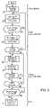
- FIG. 3shows the concatenation of the various steps of the method according to the invention in the form of a flow diagram.
- FIG. 1shows an electronic component 1 designed to be integrated into a so-called intelligent smart card.
- This componentgenerally comprises a processing unit 2 or microprocessor, connected by a communication bus 3 to memories 4 , 5 , 6 , and to a link 7 to a reading and possibly writing terminal.
- This connectionconsists either of contact areas in the case of a smart card with contacts, or an antenna in the case of a contactless smart card.
- These memoriescomprise a non-erasable memory 4 , for example of the ROM type, a non-volatile memory 5 accessible in write and read mode, for example of the EEPROM or FLASH type, and a volatile memory 6 or RAM.
- an initialisation processing 21 performed at the time of its manufactureis first of all applied to the electronic component.
- This processingconsists in writing in the memory 4 a program permitting the loading of the non-volatile memory, as well as confidential information, such as a serial number and possibly a secret key, which can alternatively be determined according to the serial number.
- the component 1is delivered to the card embedder, which in particular carries out a first phase 22 of loading the common or non-confidential data into the non-volatile memory 5 by means of the loading program stored in the memory 4 and using so-called physical, non-secure, commands which are transmitted to the microprocessor 2 by means of a personalisation terminal.
- the loading programcarries out only a check of the addresses where the data are written. These can therefore be written in any order. It is even possible to write several times to the same addresses in the memory 5 .
- this phaseit is possible to authorise the reading of the content of the memory 5 for the purpose of verification but, if a high level of security is required, such a reading may be inhibited, the data written during this phase next being verified.
- the data loaded during this phasecomprise the common or non-confidential parts 13 of an operating system and/or of application programs, a file structure 14 , and common or non-confidential information 15 , one part 12 of the memory 5 remaining free.
- some predefined areas 11 of the memory 5are left free for the storage of confidential data or programs or those specific to the user for whom the smart card is intended.
- the terminaltransmits 23 a phase change command which triggers a process of verification and validation of the data loaded into this memory and then inhibits any further loading of non-confidential information, at least in the same memory area.
- This commandadvantageously comprises a phase change instruction as well as a characteristic value such as a condensed value representing the content of the memory 5 , this value being able for example to be obtained by means of a hash function.
- the condensed valuecan be an MAC code.
- This codecan be obtained by means of a so-called hash function in combination with a secret key. It is for example possible to apply the hash function MD5 or SHA-1 (Secure Hash Algorithm-1) making it possible to calculate a binary sequence, for example of 160 bits, representing in a condensed manner the content of the memory 5 , such a function being designed so that a slight modification to the content of the memory gives rise to a significant modification to the binary sequence thus calculated.
- MD5hash function
- SHA-1Secure Hash Algorithm-1
- This phase change commandcan also be encrypted by means of a secret key, which may be the same as the previous one.
- the loading program stored in the memory 4carries out the verification 24 of the content of this memory in order to validate the integrity of all the data which were sent to the component during this phase.
- This verificationcomprises first of all the calculation of a characteristic value, applied to all or part of the memory 5 .
- the loading programcompares 25 this value thus calculated with a reference value which was transmitted in the phase change command.
- the first loading phaseis considered to have failed and an error code is transmitted to the personalisation terminal.
- the loading programthen returns to step 22 .
- this loading phaseis validated and can be followed by a phase of loading the specific or confidential data.
- This verification stepguarantees the integrity of the non-confidential data even if the loading was carried out by means of physical commands.
- the method according to the inventionmakes it possible to load the non-confidential data into the memory 5 very quickly.
- step 26 to 29the specific or confidential data to be loaded into the memory 5 are transmitted 26 to the component one after the other by the personalisation terminal, in the form of write commands which are verified 27 by the microprocessor 2 before being executed.
- each write commandcomprises the value of the data to be written, the address for writing the data in the memory, and the length of the data, as well as a redundancy code if necessary.
- the wholecan be associated with a condensed value characteristic of the command. This condensed value may be a signature.
- This signatureis for example obtained by means of a hash function.
- the binary sequence obtainedcan be encrypted by means of a key, which may be the secret key stored at step 21 in the memory 4 , in order to obtain a message authentication code or MAC.
- the whole of the commandcan also be decrypted by means of the secret key or keys installed at step 21 .
- the microprocessorOn reception of a command to write a specific or confidential data item, the microprocessor decrypts the encrypted signature associated with the command received and, if this corresponds to the command received (step 28 ), proceeds with the writing of the data item associated with the command at the address indicated.
- the microprocessor 2applies the hash function to the command received and compares the signature received and decrypted with the signature thus calculated.
- each write commandis also associated with a command number which is incremented at each write command, the microprocessor 2 accepting a loading command only if the command number corresponds to the number of the command previously received incremented by one.
- These free area addressescan also be loaded in association with a loading command number, the microprocessor also verifying at each write command whether the command number corresponds to the writing address.
- the terminaltransmits to the card an end of phase command preferably containing a phase number.
- This commandcan also be encrypted and transmitted to the microprocessor 2 in the form of an MAC signature and comprise a command number which corresponds to the number of the last loading command transmitted, incremented by one.
- phase change messagetriggers the activation 31 of the application program by the microprocessor. The latter can therefore no longer receive loading commands.
- a free personalisation phasesteps 22 to 25
- a confidential personalisation phasesteps 26 to 30
- the program for loading into the memory 4prefferably be designed to load only a first partition by executing steps 22 to 30 , and for the data loaded during the first cycle to include the loading of a second loading program specifically designed to load only the second partition, this program being activated following the reception by the microprocessor of a phase change command at the end of the secure personalisation phase of the first partition.
- Several loading cyclescomprising the execution of steps 22 to 30 can thus be concatenated, the reception of the phase change command at the end of the last cycle triggering the activation of the application program.
- the methoduses an encryption key for the secure personalisation command, specific to each entity carrying out the loading of part of the memory 5 .
Landscapes
- Engineering & Computer Science (AREA)
- Business, Economics & Management (AREA)
- Physics & Mathematics (AREA)
- General Physics & Mathematics (AREA)
- Microelectronics & Electronic Packaging (AREA)
- Computer Networks & Wireless Communication (AREA)
- Accounting & Taxation (AREA)
- Strategic Management (AREA)
- General Business, Economics & Management (AREA)
- Theoretical Computer Science (AREA)
- Storage Device Security (AREA)
Abstract
Description
- a first phase of loading information into the memory of the component,
- a validation phase comprising the verification of the information loaded into the memory of the component, and
- a second phase of loading information into the memory of the component, performed solely if the information loaded during the first loading phase is valid, this second phase comprising at least one step of loading information and validating this information.
Claims (14)
Applications Claiming Priority (4)
| Application Number | Priority Date | Filing Date | Title |
|---|---|---|---|
| FR0014633 | 2000-11-14 | ||
| FR00/14633 | 2000-11-14 | ||
| FR0014633AFR2816731B1 (en) | 2000-11-14 | 2000-11-14 | METHOD FOR LOADING AND CUSTOMIZING THE INFORMATION AND PROGRAMS LOADED IN A CHIP CARD |
| PCT/FR2001/003563WO2002041267A1 (en) | 2000-11-14 | 2001-11-14 | Method for loading and customizing data and programmes loaded in a smart card |
Publications (2)
| Publication Number | Publication Date |
|---|---|
| US20040013266A1 US20040013266A1 (en) | 2004-01-22 |
| US7725942B2true US7725942B2 (en) | 2010-05-25 |
Family
ID=8856425
Family Applications (1)
| Application Number | Title | Priority Date | Filing Date |
|---|---|---|---|
| US10/416,181Expired - Fee RelatedUS7725942B2 (en) | 2000-11-14 | 2001-11-14 | Method for loading and customizing data and programmes loaded in a smart card |
Country Status (5)
| Country | Link |
|---|---|
| US (1) | US7725942B2 (en) |
| EP (1) | EP1337981A1 (en) |
| AU (1) | AU2002218367A1 (en) |
| FR (1) | FR2816731B1 (en) |
| WO (1) | WO2002041267A1 (en) |
Cited By (4)
| Publication number | Priority date | Publication date | Assignee | Title |
|---|---|---|---|---|
| US20070143630A1 (en)* | 2005-12-16 | 2007-06-21 | Aladdin Knowledge Systems (Deutschland) Gmbh | Method and device for protecting a program comprising a functional block |
| US20120204248A1 (en)* | 2011-02-09 | 2012-08-09 | Verizon Patent And Licensing Inc. | Provisioner for single sign-on and non-single sign-on sites, applications, systems, and sessions |
| DE102018005284A1 (en)* | 2018-07-03 | 2019-09-05 | Giesecke+Devrient Mobile Security Gmbh | Chip personalization of an embedded system by a third party |
| US10776457B1 (en)* | 2014-07-22 | 2020-09-15 | Epic Games, Inc. | System and method for preventing execution of unauthorized code |
Families Citing this family (8)
| Publication number | Priority date | Publication date | Assignee | Title |
|---|---|---|---|---|
| JP4426492B2 (en)* | 2005-03-30 | 2010-03-03 | Ykk株式会社 | Programmable terminal system |
| DE102005022019A1 (en)* | 2005-05-12 | 2007-02-01 | Giesecke & Devrient Gmbh | Secure processing of data |
| KR100745603B1 (en)* | 2006-02-08 | 2007-08-02 | 삼성전자주식회사 | Secure multimedia card and memory card system including same |
| US7575485B2 (en)* | 2007-02-16 | 2009-08-18 | Fci Americas Technology, Inc. | Knurled inner sleeve for a cable connector |
| KR100997238B1 (en)* | 2008-03-03 | 2010-11-29 | 삼성전자주식회사 | CRUM unit, replaceable unit and image forming apparatus using same, authentication and encryption data communication method thereof |
| FR3083341B1 (en)* | 2018-06-28 | 2020-09-18 | Idemia France | CONFIGURATION OF AN ELECTRONIC DEVICE |
| US11641274B2 (en)* | 2019-03-22 | 2023-05-02 | Jpmorgan Chase Bank, N.A. | Systems and methods for manipulation of private information on untrusted environments |
| US12432071B2 (en)* | 2020-07-15 | 2025-09-30 | Micron Technology, Inc. | Secure serial peripheral interface (SPI) flash |
Citations (16)
| Publication number | Priority date | Publication date | Assignee | Title |
|---|---|---|---|---|
| US4493073A (en)* | 1982-08-30 | 1985-01-08 | At&T Bell Laboratories | Maintenance of stored program controlled switching systems |
| US4742215A (en)* | 1986-05-07 | 1988-05-03 | Personal Computer Card Corporation | IC card system |
| US4862501A (en)* | 1985-03-08 | 1989-08-29 | Kabushiki Kaisha Toshiba | Communications network using IC cards |
| US5410690A (en) | 1989-11-30 | 1995-04-25 | Kabushiki Kaisha Toshiba | System for issuing portable storage media containing common and individual data |
| US5452431A (en)* | 1991-10-30 | 1995-09-19 | U.S. Philips Corporation | Microcircuit for a chip card comprising a protected programmable memory |
| EP0798673A1 (en) | 1996-03-29 | 1997-10-01 | Koninklijke KPN N.V. | Method of securely loading commands in a smart card |
| US5727230A (en)* | 1994-04-28 | 1998-03-10 | Mitsubishi Denki Kabushiki Kaisha | Apparatus for electromagnetic communication between a computer and a non-contact IC card |
| WO1999010848A1 (en) | 1997-08-21 | 1999-03-04 | Activcard | Portable electronic device for safe communication system, and method for initialising its parameters |
| US5917168A (en)* | 1993-06-02 | 1999-06-29 | Hewlett-Packard Company | System and method for revaluation of stored tokens in IC cards |
| US5923884A (en)* | 1996-08-30 | 1999-07-13 | Gemplus S.C.A. | System and method for loading applications onto a smart card |
| US6005942A (en)* | 1997-03-24 | 1999-12-21 | Visa International Service Association | System and method for a multi-application smart card which can facilitate a post-issuance download of an application onto the smart card |
| US6097967A (en)* | 1997-08-14 | 2000-08-01 | Alcatel | Method of downloading a predetermined list of items into a mobile terminal controlled by a subscriber identity module, and a command, a subscriber identity module, and a mobile terminal corresponding to the method |
| US6357665B1 (en)* | 1998-01-22 | 2002-03-19 | Mondex International Limited | Configuration of IC card |
| US6694436B1 (en)* | 1998-05-22 | 2004-02-17 | Activcard | Terminal and system for performing secure electronic transactions |
| US6931379B1 (en)* | 2000-08-11 | 2005-08-16 | Hitachi, Ltd. | IC card system and IC card |
| US7117364B1 (en)* | 1999-10-05 | 2006-10-03 | International Busienss Machines Corporation | System and method for downloading application components to a chipcard |
Family Cites Families (1)
| Publication number | Priority date | Publication date | Assignee | Title |
|---|---|---|---|---|
| US6216227B1 (en)* | 1998-06-29 | 2001-04-10 | Sun Microsystems, Inc. | Multi-venue ticketing using smart cards |
- 2000
- 2000-11-14FRFR0014633Apatent/FR2816731B1/ennot_activeExpired - Fee Related
- 2001
- 2001-11-14USUS10/416,181patent/US7725942B2/ennot_activeExpired - Fee Related
- 2001-11-14AUAU2002218367Apatent/AU2002218367A1/ennot_activeAbandoned
- 2001-11-14EPEP01996837Apatent/EP1337981A1/ennot_activeWithdrawn
- 2001-11-14WOPCT/FR2001/003563patent/WO2002041267A1/ennot_activeApplication Discontinuation
Patent Citations (16)
| Publication number | Priority date | Publication date | Assignee | Title |
|---|---|---|---|---|
| US4493073A (en)* | 1982-08-30 | 1985-01-08 | At&T Bell Laboratories | Maintenance of stored program controlled switching systems |
| US4862501A (en)* | 1985-03-08 | 1989-08-29 | Kabushiki Kaisha Toshiba | Communications network using IC cards |
| US4742215A (en)* | 1986-05-07 | 1988-05-03 | Personal Computer Card Corporation | IC card system |
| US5410690A (en) | 1989-11-30 | 1995-04-25 | Kabushiki Kaisha Toshiba | System for issuing portable storage media containing common and individual data |
| US5452431A (en)* | 1991-10-30 | 1995-09-19 | U.S. Philips Corporation | Microcircuit for a chip card comprising a protected programmable memory |
| US5917168A (en)* | 1993-06-02 | 1999-06-29 | Hewlett-Packard Company | System and method for revaluation of stored tokens in IC cards |
| US5727230A (en)* | 1994-04-28 | 1998-03-10 | Mitsubishi Denki Kabushiki Kaisha | Apparatus for electromagnetic communication between a computer and a non-contact IC card |
| EP0798673A1 (en) | 1996-03-29 | 1997-10-01 | Koninklijke KPN N.V. | Method of securely loading commands in a smart card |
| US5923884A (en)* | 1996-08-30 | 1999-07-13 | Gemplus S.C.A. | System and method for loading applications onto a smart card |
| US6005942A (en)* | 1997-03-24 | 1999-12-21 | Visa International Service Association | System and method for a multi-application smart card which can facilitate a post-issuance download of an application onto the smart card |
| US6097967A (en)* | 1997-08-14 | 2000-08-01 | Alcatel | Method of downloading a predetermined list of items into a mobile terminal controlled by a subscriber identity module, and a command, a subscriber identity module, and a mobile terminal corresponding to the method |
| WO1999010848A1 (en) | 1997-08-21 | 1999-03-04 | Activcard | Portable electronic device for safe communication system, and method for initialising its parameters |
| US6357665B1 (en)* | 1998-01-22 | 2002-03-19 | Mondex International Limited | Configuration of IC card |
| US6694436B1 (en)* | 1998-05-22 | 2004-02-17 | Activcard | Terminal and system for performing secure electronic transactions |
| US7117364B1 (en)* | 1999-10-05 | 2006-10-03 | International Busienss Machines Corporation | System and method for downloading application components to a chipcard |
| US6931379B1 (en)* | 2000-08-11 | 2005-08-16 | Hitachi, Ltd. | IC card system and IC card |
Cited By (5)
| Publication number | Priority date | Publication date | Assignee | Title |
|---|---|---|---|---|
| US20070143630A1 (en)* | 2005-12-16 | 2007-06-21 | Aladdin Knowledge Systems (Deutschland) Gmbh | Method and device for protecting a program comprising a functional block |
| US8495388B2 (en)* | 2005-12-16 | 2013-07-23 | Sfnt Germany Gmbh | Method and device for protecting a program comprising a functional block |
| US20120204248A1 (en)* | 2011-02-09 | 2012-08-09 | Verizon Patent And Licensing Inc. | Provisioner for single sign-on and non-single sign-on sites, applications, systems, and sessions |
| US10776457B1 (en)* | 2014-07-22 | 2020-09-15 | Epic Games, Inc. | System and method for preventing execution of unauthorized code |
| DE102018005284A1 (en)* | 2018-07-03 | 2019-09-05 | Giesecke+Devrient Mobile Security Gmbh | Chip personalization of an embedded system by a third party |
Also Published As
| Publication number | Publication date |
|---|---|
| WO2002041267A1 (en) | 2002-05-23 |
| US20040013266A1 (en) | 2004-01-22 |
| FR2816731A1 (en) | 2002-05-17 |
| AU2002218367A1 (en) | 2002-05-27 |
| EP1337981A1 (en) | 2003-08-27 |
| FR2816731B1 (en) | 2003-01-03 |
Similar Documents
| Publication | Publication Date | Title |
|---|---|---|
| US7469837B2 (en) | Storage device | |
| US5513261A (en) | Key management scheme for use with electronic cards | |
| US6073238A (en) | Method of securely loading commands in a smart card | |
| EP0707270B1 (en) | Method and apparatus for validating system operation | |
| US7617528B2 (en) | Smartcard with protected memory access | |
| RU2224288C2 (en) | Intercept-protected memory device | |
| US7260727B2 (en) | Method for secure storage of sensitive data in a memory of an embedded microchip system, particularly a smart card, and embedded system implementing the method | |
| US5533126A (en) | Key protection device for smart cards | |
| JP3613687B2 (en) | PC card for microcomputer | |
| US7725942B2 (en) | Method for loading and customizing data and programmes loaded in a smart card | |
| JPH11506240A (en) | How to securely change smart card data | |
| JP2002373116A (en) | Method for protecting microcomputer system, memory device, computer program, smart card and microcomputer system | |
| CN115454517B (en) | Method, system, storage medium, device and chip for multi-medium secure boot | |
| KR20170102285A (en) | Security Elements | |
| KR100300794B1 (en) | How to enter information on the chip card | |
| US7299366B2 (en) | Secure software customization for smartcard | |
| US10853476B2 (en) | Method for the security of an electronic operation | |
| JP4899499B2 (en) | IC card issuing method, IC card issuing system, and IC card | |
| US9659425B2 (en) | Electronic key for authentication | |
| US20100211727A1 (en) | integrated circuit board with secured input/output buffer | |
| JP2007011591A (en) | Portable electronic device and IC card | |
| 台灣銘板股份有限公司 | TNP ECC2 CPU Card Security Target |
Legal Events
| Date | Code | Title | Description |
|---|---|---|---|
| AS | Assignment | Owner name:GEMPLUS, FRANCE Free format text:ASSIGNMENT OF ASSIGNORS INTEREST;ASSIGNOR:GIRAUD, JEAN-LUC;REEL/FRAME:014414/0360 Effective date:20030424 Owner name:GEMPLUS,FRANCE Free format text:ASSIGNMENT OF ASSIGNORS INTEREST;ASSIGNOR:GIRAUD, JEAN-LUC;REEL/FRAME:014414/0360 Effective date:20030424 | |
| AS | Assignment | Owner name:GEMALTO SA,FRANCE Free format text:MERGER;ASSIGNOR:GEMPLUS;REEL/FRAME:024193/0424 Effective date:20081001 | |
| STCF | Information on status: patent grant | Free format text:PATENTED CASE | |
| AS | Assignment | Owner name:GEMALTO SA, FRANCE Free format text:MERGER;ASSIGNOR:GEMPLUS;REEL/FRAME:024906/0868 Effective date:20081001 | |
| FPAY | Fee payment | Year of fee payment:4 | |
| MAFP | Maintenance fee payment | Free format text:PAYMENT OF MAINTENANCE FEE, 8TH YEAR, LARGE ENTITY (ORIGINAL EVENT CODE: M1552) Year of fee payment:8 | |
| FEPP | Fee payment procedure | Free format text:MAINTENANCE FEE REMINDER MAILED (ORIGINAL EVENT CODE: REM.); ENTITY STATUS OF PATENT OWNER: LARGE ENTITY | |
| LAPS | Lapse for failure to pay maintenance fees | Free format text:PATENT EXPIRED FOR FAILURE TO PAY MAINTENANCE FEES (ORIGINAL EVENT CODE: EXP.); ENTITY STATUS OF PATENT OWNER: LARGE ENTITY | |
| STCH | Information on status: patent discontinuation | Free format text:PATENT EXPIRED DUE TO NONPAYMENT OF MAINTENANCE FEES UNDER 37 CFR 1.362 | |
| FP | Lapsed due to failure to pay maintenance fee | Effective date:20220525 |