US7724857B2 - Method and apparatus for improving linearity in clock and data recovery systems - Google Patents
Method and apparatus for improving linearity in clock and data recovery systemsDownload PDFInfo
- Publication number
- US7724857B2 US7724857B2US11/375,828US37582806AUS7724857B2US 7724857 B2US7724857 B2US 7724857B2US 37582806 AUS37582806 AUS 37582806AUS 7724857 B2US7724857 B2US 7724857B2
- Authority
- US
- United States
- Prior art keywords
- interpolator
- phase
- input
- output signal
- signal
- Prior art date
- Legal status (The legal status is an assumption and is not a legal conclusion. Google has not performed a legal analysis and makes no representation as to the accuracy of the status listed.)
- Expired - Fee Related, expires
Links
Images


Classifications
- H—ELECTRICITY
- H04—ELECTRIC COMMUNICATION TECHNIQUE
- H04L—TRANSMISSION OF DIGITAL INFORMATION, e.g. TELEGRAPHIC COMMUNICATION
- H04L7/00—Arrangements for synchronising receiver with transmitter
- H04L7/0008—Synchronisation information channels, e.g. clock distribution lines
Definitions
- the present inventionrelates generally to clock and data recovery (CDR) systems and more specifically to improving interpolator linearity in CDR systems.
- Clock and data recovery (CDR) operationsare performed in many communication circuits.
- Digital communication receiverssample an analog waveform and then detect the data that the waveform represents.
- the phase of the analog waveformis typically unknown and there may be a frequency offset between the frequency at which the original data was transmitted and the nominal receiver sampling clock frequency.
- the CDR functionis used to properly sample an analog waveform using a reference clock to correctly recover the data.
- FIG. 1shows a block diagram of a prior art CDR circuit 100 .
- the CDR circuit 100receives as input a reference clock 140 and an analog data stream 104 that represents digital bits (i.e., 1s and 0s), and provides as output a recovered clock 110 and recovered data 106 .
- the data stream 104is often a differential waveform as represented by waveform 108 .
- the differential waveform 108has multiple so-called “eyes” 112 which represent the maximum and minimum amplitude of the data stream 104 during a time interval.
- the waveform 108has transition points, such as transition points 120 , 124 , that indicate the transition from one eye to the next. Each eye also has a respective midpoint (e.g., midpoint 116 of eye 112 ).
- the CDR circuit 100includes a series of latches 134 that are clocked from a clock signal 126 to sample the data stream 104 at the midpoint 116 of the eye 112 .
- the midpoint 116 of the eye 112is typically sampled because the CDR circuit often has the best chance of correctly identifying whether the waveform is representing a digital 0 or a digital 1 at that instant in time.
- the CDR circuit 100determines each transition point (e.g., transition point 120 and 124 ) and the midpoint 116 of the eye 112 .
- the data signalmay shift in time during the transmission relative to the clock signal. This shifting in time may result in the differential waveform 108 moving (back and forth or in one direction over time with respect to the reference clock 140 ) as it is being received by the CDR circuit 100 .
- the CDR circuit 100determines this time shifting in order to ensure that the CDR circuit 100 samples each eye 112 of the waveform 108 at its midpoint 116 .
- the CDR circuit 100determines the transition point 120 and 124 and midpoint 116 of each eye 112 and then changes the phase of an output signal 126 of an interpolator 128 of the CDR circuit 100 , via a control signal 130 .
- the CDR circuit 100samples the input data stream 104 at points determined by the phase of the output signal 126 of the interpolator.
- input clock signal 140is delayed, creating a new clock signal 144 .
- These clock phasesare connected to each input 132 , 136 of the interpolator 128 .
- one input clock signal 144is delayed with respect to the other input clock signal 140 .
- These two input signalsprovide the minimum phase and the maximum phase for the interpolator 128 .
- the input impedance of each input 132 , 136 of the interpolator 128also changes. This variation in input impedance results in an amplitude variation of the input clock signals 140 , 144 . This, in turn, results in an undesirable change in the phase of the input clock signals 140 , 144 relative to each other.
- the prior art interpolatordoes not change phases in a smooth, linear manner. Instead, the phase of the prior art interpolator's output signal 126 changes as a result of an impedance variation with respect to the interpolator's inputs. As a result, the input data stream 104 may not be sampled correctly.
- an interpolator of a clock and data recovery (CDR) circuitis designed to have a linear delay change as the phase of its output signal changes from one phase to the next.
- a CDR circuitreceives a data stream and adjusts a phase of a clock signal using two interpolators. The data stream is then recovered using the clock signal.
- the CDR circuithas a first interpolator that includes a first input for receiving a first input signal and a second input for receiving a second input signal.
- the CDR circuitalso has a second interpolator that includes a first input for receiving the first input signal and a second input for receiving the second input signal.
- the first interpolatorincludes an output connected to a delay loop that comprises a plurality of delay cells. In one embodiment, the first interpolator's output is connected with one of a first portion of the plurality of delay cells. Similarly, the second interpolator includes an output connected with the delay loop. In one embodiment, the second interpolator's output is connected to a second portion of the plurality of delay cells.
- the first input signalis a first clock signal and the second input signal is a second clock signal.
- the second clock signalis delayed by a delay cell with respect to the first clock signal.
- the phase of the output signal of the second interpolatoris adjusted simultaneously with and complementarily to the adjusting of the phase of the first interpolator.
- the first interpolator's output signalis injected into a first delay cell in the plurality of delay cells and the output of the second interpolator is inactivated.
- the second interpolator's output signalis injected into another one of the delay cells in the plurality of delay cells. The first interpolator's output signal is inactivated.
- FIG. 1is a block diagram of a prior art clock and data recovery (CDR) circuit
- FIG. 2Ais a more detailed block diagram of a prior art CDR circuit
- FIG. 2Bshows timing diagrams of input and output signals of an interpolator in the prior art CDR circuit of FIG. 2A ;
- FIG. 3shows a block diagram of a CDR circuit in accordance with an embodiment of the present invention.
- FIG. 4is a flowchart of the steps performed by a CDR circuit in accordance with an embodiment of the present invention.
- FIG. 2Ashows a more detailed block diagram of a prior art CDR 200 .
- the CDR 200includes a fixed reference clock signal 202 .
- the CDR 200also includes an interpolator 204 having inputs A 208 and B 212 and output Z 213 .
- the interpolator 204has a control 216 that enables the programming of the interpolator 204 to output a signal having one of a predetermined number of phases, such as one of 16 different phase possibilities.
- the control 216is a digital control.
- control 216enables the programming of the phase of the output signal of the interpolator 204 .
- the inputs A 208 and B 212 of the interpolator 204receive two signals having different phases. One input corresponds to one extreme of the possible phases that the output signal can have while the other input corresponds with the other extreme of the possible phases that the output signal can have.
- a delay cell 218 before the input B 212 of the interpolator 204is included to delay the clock signal received by input B 212 with respect to the clock signal received by input A 208 .
- the delay cell 218can be located at input A 208 or input B 212 .
- FIG. 2Bshows timing diagrams representing the clock signal 202 and the inputs 208 , 212 and output 213 of the interpolator 204 .
- the clock signal 202 and, therefore, input A 208can be represented by a first waveform 220 .
- Input B 212has been delayed a predetermined time 224 because of delay cell 218 .
- the waveform that is provided into input B 212is shown as waveform 228 .
- the delay or phase associated with waveform 232 that is the output of output Z 213can be varied from the starting phase associated with waveform 220 to the ending phase (i.e., delay 224 ) of the waveform 228 .
- the possible start phase and end phase of waveform 232is controlled by the control 216 of the interpolator 204 and can be anywhere between time t 1 234 and time t 2 235 . If the control 216 is set to its minimum value, the interpolator's output Z 213 is the same as the waveform 220 . If the control 216 is set to its maximum value, the interpolator's output Z 213 is the same as the waveform 228 . These phase variations are shown with numerous lines in waveform 232 .
- the CDR 200includes delay loop 236 having output delay cells 237 , 238 , 239 , 240 .
- Output signal 242 of output Z 213is delayed by one or more delay cells 237 - 240 of the delay loop 236 .
- the output signal 242is provided to one of the delay cells 237 - 240 and is then propagated through the rest of the delay cells 237 - 240 in the loop 236 .
- the output signal 242then travels to delay cell 239 , then to delay cell 240 , and then wraps around to delay cell 237 .
- Each delay cell 218 , 237 - 240can have a predetermined delay or can be set by an external signal or circuit.
- the output of each delay cell 237 - 240represents the location of either a transition point (e.g., transition points 244 , 252 ) of an eye 248 or the midpoint 256 of the eye 248 .
- the amount of delay corresponding with the delay cell 218 , 237 - 240is equal to half of a unit interval (UI), where a unit interval is the time associated with each eye (e.g., eye 248 ).
- UIunit interval
- Specialized control logicin the CDR monitors the centering of the sampling and transition clocks with respect to the data stream. If the clocks become uncentered with respect to the data stream (e.g. the data stream is delayed from the sampling clocks), the interpolator 204 is instructed via the control 216 to further delay the phase of its output signal. Eventually, the phase of the output signal 242 reaches its maximum delay (i.e., waveform 232 matches waveform 228 ). If the CDR 200 determines that additional phase delays are needed to sample the midpoint 256 , the control 216 resets the interpolator 204 back to the starting phase.
- the injection point of the output signal 242 into the delay loop 236is moved back a delay cell 237 - 240 .
- the interpolator 204used an injection point 260 to sample the midpoint 256 and the control 216 resets the phase back to the beginning phase, then the injection point is also changed to a second injection point 264 so that there are now two delay cells before sampling the midpoint 256 . This is to prevent a large jump in phase when the control 216 reaches the last setting for the phase.
- the disadvantages associated with the prior art CDR architectureis as follows.
- the phase of the interpolator 204is adjusted by changing the dc bias on the circuitry associated with the interpolator inputs A 208 and B 212 .
- the phase of the output 213 (i.e., output signal 242 ) of the interpolator 204is adjusted from one extreme to the other, the input impedance of each input A 208 and B 212 of the interpolator 204 also changes.
- the change in input impedanceresults in an amplitude and phase variation of the input clock signal 202 based on the impedance at each input 208 , 212 .
- the amplitude and phase of the input clock signal 202also varies. This, in turn, results in a change in the delay 224 between the two clock signals provided to the two inputs 208 , 212 .
- the delay 224is important because it is used to generate the predetermined number of output phases.
- FIG. 3shows a block diagram of a CDR circuit 300 in accordance with an embodiment of the present invention.
- a reference clock signal 304provides the input clock signal to two interpolators 308 a , 308 b .
- Each interpolator 308 a , 308 bhas an A input (e.g., a first A input 312 for interpolator 308 a and a second A input (not shown)) for interpolator 308 b and a B input (e.g., a first B input 316 a for interpolator 308 a and a second B input 316 b for interpolator 308 b ).
- Each interpolator 308 a , 308 balso includes a Z output 320 a , 320 b and a control 322 a , 322 b , respectively.
- clock signal 328is provided to the A input of each interpolator 308 a , 308 b .
- clock signal 332(after delay cell 324 ) is provided to the B input of each interpolator 308 a , 308 b.
- the CDR circuit 300includes first delay cell 324 positioned before the B inputs of the interpolators 308 a , 308 b to provide delay between the clock signal 332 provided to the B inputs and the clock signal 328 provided to the A inputs of the interpolators 308 a , 308 b .
- the CDR circuit 300also includes delay loop 336 having delay cells 350 - 354 .
- one interpolator's outputis active while the other interpolator's output is set to be inactive.
- a multiplexorMUX
- MUXmultiplexor
- the active interpolator's phaseis then changed from one extreme (e.g., a minimum phase delay) to the other (e.g., a maximum phase delay). For example, suppose the first interpolator 308 a is active (i.e., its output is active) while the second interpolator 308 b is inactive (i.e., its output is inactive). Also suppose that each control 322 a , 322 b accepts a four bit word as its input. The first control 322 a is adjusted from the first extreme (e.g., 0000) to the second extreme (e.g., 1111) to vary the phase of the first interpolator 308 a.
- first extremee.g., 0000
- the second extremee.g., 1111
- the inactive interpolator's phase control 322 bis adjusted in a complementary manner. This means that the phase of the inactive interpolator is adjusted in the opposite direction as the phase of the active interpolator.
- the value of the inactive interpolator's phase controlis the inverse of the value of the active interpolator's phase control.
- the second control 322 bis therefore adjusted from the second extreme (e.g., 1111) to the first extreme (e.g., 0000).
- this second interpolator 308 bis not being used (i.e., its output 320 b is inactive)
- the input impedance associated with the A input of the first interpolator 308 ais adjusted in the opposite direction as the input impedance associated with the A input of the second interpolator 308 b .
- the input impedance associated with the B input of each interpolator 308 a , 308 bis also adjusted in opposite directions. Because the input impedances of the same input for each interpolator 308 a , 308 b are adjusted in opposite directions, they end up balancing each other out (because the same inputs on each interpolator are connected together in parallel) and remain relatively constant.
- the amplitude and phase associated with each input signal 328 , 332remains relatively constant because the input impedance remains relatively constant as the phase is varied for each interpolator 308 a , 308 b .
- the delay between the A and B inputs of the interpolators 308 a , 308 balso remains relatively constant because of the balancing of the impedance.
- the injection pointis set to delay cell 350 .
- the first interpolator 308 astarts at the lowest phase and the control 322 a increments the phase up to the maximum phase.
- the phase of the second interpolator 308 bis transitioned from the maximum phase down to the minimum phase.
- the injection pointis then changed to second delay cell 354 , the first interpolator 308 a is made inactive, and the second interpolator 308 b is made active.
- the normal transition time needed to transition one interpolator from its maximum phase back to its minimum phaseis eliminated because the second interpolator is already at the minimum phase (i.e., the starting point for the new injection point).
- each interpolator 308 a , 308 bis connected to two delay cells 336 while the prior art interpolator is connected to all four delay cells. This results in less loading on the output of each interpolator 308 a , 308 b.
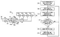
- FIG. 4is a flowchart showing the steps performed by the CDR circuit 300 to provide a linear transition between phase changes.
- One interpolatoris selected to inject its output signal (e.g., a first output signal 340 or a second output signal 344 ) into delay line 336 in step 404 .
- the phase control for the selected interpolatoris adjusted in step 408 .
- the other interpolator's phaseis adjusted in a complementary manner with respect to the selected interpolator in step 412 .
- the circuitdetermines whether the maximum extreme has been reached with respect to the selected interpolator in step 416 . If not, the phase for each interpolator is incremented again.
- the circuitthen moves the injection point to the previous delay cell in step 420 and then switches the active and inactive interpolators in step 424 .
- the interpolator that recently became the active interpolatorwas at the minimum phase setting. The process repeats itself by returning to step 408 . Note that phase changes in the interpolator and injection point changes can move in either direction, as needed to center the sampling clocks on the midpoint of the data eye.
Landscapes
- Engineering & Computer Science (AREA)
- Computer Networks & Wireless Communication (AREA)
- Signal Processing (AREA)
- Stabilization Of Oscillater, Synchronisation, Frequency Synthesizers (AREA)
- Pulse Circuits (AREA)
Abstract
Description
Claims (30)
Priority Applications (2)
| Application Number | Priority Date | Filing Date | Title |
|---|---|---|---|
| US11/375,828US7724857B2 (en) | 2006-03-15 | 2006-03-15 | Method and apparatus for improving linearity in clock and data recovery systems |
| US12/755,522US8385493B2 (en) | 2006-03-15 | 2010-04-07 | Method and apparatus for improving linearity in clock and data recovery systems |
Applications Claiming Priority (1)
| Application Number | Priority Date | Filing Date | Title |
|---|---|---|---|
| US11/375,828US7724857B2 (en) | 2006-03-15 | 2006-03-15 | Method and apparatus for improving linearity in clock and data recovery systems |
Related Child Applications (1)
| Application Number | Title | Priority Date | Filing Date |
|---|---|---|---|
| US12/755,522ContinuationUS8385493B2 (en) | 2006-03-15 | 2010-04-07 | Method and apparatus for improving linearity in clock and data recovery systems |
Publications (2)
| Publication Number | Publication Date |
|---|---|
| US20070217558A1 US20070217558A1 (en) | 2007-09-20 |
| US7724857B2true US7724857B2 (en) | 2010-05-25 |
Family
ID=38517819
Family Applications (2)
| Application Number | Title | Priority Date | Filing Date |
|---|---|---|---|
| US11/375,828Expired - Fee RelatedUS7724857B2 (en) | 2006-03-15 | 2006-03-15 | Method and apparatus for improving linearity in clock and data recovery systems |
| US12/755,522Expired - Fee RelatedUS8385493B2 (en) | 2006-03-15 | 2010-04-07 | Method and apparatus for improving linearity in clock and data recovery systems |
Family Applications After (1)
| Application Number | Title | Priority Date | Filing Date |
|---|---|---|---|
| US12/755,522Expired - Fee RelatedUS8385493B2 (en) | 2006-03-15 | 2010-04-07 | Method and apparatus for improving linearity in clock and data recovery systems |
Country Status (1)
| Country | Link |
|---|---|
| US (2) | US7724857B2 (en) |
Cited By (1)
| Publication number | Priority date | Publication date | Assignee | Title |
|---|---|---|---|---|
| US11606082B2 (en) | 2021-05-20 | 2023-03-14 | International Business Machines Corporation | Adjustable phase shifter |
Families Citing this family (7)
| Publication number | Priority date | Publication date | Assignee | Title |
|---|---|---|---|---|
| US9112625B2 (en)* | 2010-06-21 | 2015-08-18 | Guansong Zhang | Method and apparatus for emulating stream clock signal in asynchronous data transmission |
| US9191245B2 (en) | 2011-03-08 | 2015-11-17 | Tektronix, Inc. | Methods and systems for providing optimum decision feedback equalization of high-speed serial data links |
| US8855186B2 (en)* | 2011-03-08 | 2014-10-07 | Tektronix, Inc. | Methods and systems for providing optimum decision feedback equalization of high-speed serial data links |
| US9559880B1 (en)* | 2016-03-04 | 2017-01-31 | Inphi Corporation | Eye modulation for pulse-amplitude modulation communication systems |
| TWI628918B (en)* | 2016-09-05 | 2018-07-01 | 創意電子股份有限公司 | Clock data recovery module |
| US9800438B1 (en)* | 2016-10-25 | 2017-10-24 | Xilinx, Inc. | Built-in eye scan for ADC-based receiver |
| US10547475B1 (en)* | 2019-02-22 | 2020-01-28 | Cadence Design Systems, Inc. | System and method for measurement and adaptation of pulse response cursors to non zero values |
Citations (11)
| Publication number | Priority date | Publication date | Assignee | Title |
|---|---|---|---|---|
| US6380774B2 (en)* | 2000-03-24 | 2002-04-30 | Nec Corporation | Clock control circuit and clock control method |
| US20020053931A1 (en)* | 2000-11-06 | 2002-05-09 | Nec Corporation | Phase difference signal generator and multi-phase clock signal generator having phase interpolator |
| US6397042B1 (en)* | 1998-03-06 | 2002-05-28 | Texas Instruments Incorporated | Self test of an electronic device |
| US20030161430A1 (en) | 2002-02-26 | 2003-08-28 | Fujitsu Limited | Clock recovery circuitry |
| US6693985B2 (en) | 2000-10-27 | 2004-02-17 | Silicon Image | Clock and data recovery method and apparatus |
| US20040066873A1 (en)* | 2002-10-05 | 2004-04-08 | Cho Geun-Hee | Delay locked loop circuit for internally correcting duty cycle and duty cycle correction method thereof |
| US20040202266A1 (en) | 2003-03-26 | 2004-10-14 | Peter Gregorius | Clock and data recovery unit |
| US20050088211A1 (en)* | 2003-10-24 | 2005-04-28 | Kim Kyu-Hyoun | Jitter suppressing delay locked loop circuits and related methods |
| US20050238126A1 (en) | 2004-04-21 | 2005-10-27 | Kawasaki Lsi U.S.A., Inc. | Multi rate clock data recovery based on multi sampling technique |
| US7038510B2 (en)* | 2004-07-02 | 2006-05-02 | Broadcom Corporation | Phase adjustment method and circuit for DLL-based serial data link transceivers |
| US7403584B2 (en)* | 2003-12-31 | 2008-07-22 | Intel Corporation | Programmable phase interpolator adjustment for ideal data eye sampling |
- 2006
- 2006-03-15USUS11/375,828patent/US7724857B2/ennot_activeExpired - Fee Related
- 2010
- 2010-04-07USUS12/755,522patent/US8385493B2/ennot_activeExpired - Fee Related
Patent Citations (11)
| Publication number | Priority date | Publication date | Assignee | Title |
|---|---|---|---|---|
| US6397042B1 (en)* | 1998-03-06 | 2002-05-28 | Texas Instruments Incorporated | Self test of an electronic device |
| US6380774B2 (en)* | 2000-03-24 | 2002-04-30 | Nec Corporation | Clock control circuit and clock control method |
| US6693985B2 (en) | 2000-10-27 | 2004-02-17 | Silicon Image | Clock and data recovery method and apparatus |
| US20020053931A1 (en)* | 2000-11-06 | 2002-05-09 | Nec Corporation | Phase difference signal generator and multi-phase clock signal generator having phase interpolator |
| US20030161430A1 (en) | 2002-02-26 | 2003-08-28 | Fujitsu Limited | Clock recovery circuitry |
| US20040066873A1 (en)* | 2002-10-05 | 2004-04-08 | Cho Geun-Hee | Delay locked loop circuit for internally correcting duty cycle and duty cycle correction method thereof |
| US20040202266A1 (en) | 2003-03-26 | 2004-10-14 | Peter Gregorius | Clock and data recovery unit |
| US20050088211A1 (en)* | 2003-10-24 | 2005-04-28 | Kim Kyu-Hyoun | Jitter suppressing delay locked loop circuits and related methods |
| US7403584B2 (en)* | 2003-12-31 | 2008-07-22 | Intel Corporation | Programmable phase interpolator adjustment for ideal data eye sampling |
| US20050238126A1 (en) | 2004-04-21 | 2005-10-27 | Kawasaki Lsi U.S.A., Inc. | Multi rate clock data recovery based on multi sampling technique |
| US7038510B2 (en)* | 2004-07-02 | 2006-05-02 | Broadcom Corporation | Phase adjustment method and circuit for DLL-based serial data link transceivers |
Cited By (1)
| Publication number | Priority date | Publication date | Assignee | Title |
|---|---|---|---|---|
| US11606082B2 (en) | 2021-05-20 | 2023-03-14 | International Business Machines Corporation | Adjustable phase shifter |
Also Published As
| Publication number | Publication date |
|---|---|
| US20100195777A1 (en) | 2010-08-05 |
| US20070217558A1 (en) | 2007-09-20 |
| US8385493B2 (en) | 2013-02-26 |
Similar Documents
| Publication | Publication Date | Title |
|---|---|---|
| US8385493B2 (en) | Method and apparatus for improving linearity in clock and data recovery systems | |
| CN101202614B (en) | Systems, arrangements and methods for generating clock sample signal | |
| US5550860A (en) | Digital phase alignment and integrated multichannel transceiver employing same | |
| US8433020B2 (en) | High-speed serial data transceiver and related methods | |
| EP2131523B1 (en) | Clock data restoration device | |
| US6374361B1 (en) | Skew-insensitive low voltage differential receiver | |
| WO2005093443A1 (en) | Test device and test method | |
| US6701466B1 (en) | Serial data communication receiver having adaptively minimized capture latch offset voltage | |
| US7916822B2 (en) | Method and apparatus for reducing latency in a clock and data recovery (CDR) circuit | |
| US20080320324A1 (en) | Data recovery (CDR) architecture using interpolator and timing loop module | |
| US20120287983A1 (en) | Methods and apparatus for pseudo asynchronous testing of receive path in serializer/deserializer devices | |
| US7977989B2 (en) | Method and apparatus for detecting and adjusting characteristics of a signal | |
| US7197053B1 (en) | Serializer with programmable delay elements | |
| CN119853681A (en) | Clock and data recovery circuit and method for clock and data recovery | |
| US7991097B2 (en) | Method and apparatus for adjusting serial data signal | |
| US6570420B1 (en) | Programmable current source adjustment of leakage current for delay locked loop | |
| US20030081712A1 (en) | Data extraction circuit used for serial transmission of data signals between communication devices having different clock signal sources | |
| EP2775680B1 (en) | Sending and Receiving System, Method of Sending and Receiving, and Receiving Apparatus | |
| US20060125665A1 (en) | System and method of oversampling high speed clock/data recovery | |
| US20050228605A1 (en) | Devices and methods for testing clock and data recovery devices | |
| US7353419B1 (en) | Apparatus and method to balance set-up and hold times | |
| US20030210755A1 (en) | Data and clock synchronization in multi-channel communications | |
| KR100753246B1 (en) | Receiving apparatus and method of same, recording apparatus and method of same, and data recording system | |
| US20050093604A1 (en) | Apparatus and method for generating a phase delay | |
| JPS5819056A (en) | Clock reproducing circuit |
Legal Events
| Date | Code | Title | Description |
|---|---|---|---|
| AS | Assignment | Owner name:AGERE SYSTEMS INC., PENNSYLVANIA Free format text:ASSIGNMENT OF ASSIGNORS INTEREST;ASSIGNORS:ABEL, CHRISTOPHER;ANIDJAR, JOSEPH;SINDALOVSKY, VLADIMIR;AND OTHERS;REEL/FRAME:017699/0576 Effective date:20060313 Owner name:AGERE SYSTEMS INC.,PENNSYLVANIA Free format text:ASSIGNMENT OF ASSIGNORS INTEREST;ASSIGNORS:ABEL, CHRISTOPHER;ANIDJAR, JOSEPH;SINDALOVSKY, VLADIMIR;AND OTHERS;REEL/FRAME:017699/0576 Effective date:20060313 | |
| FPAY | Fee payment | Year of fee payment:4 | |
| AS | Assignment | Owner name:DEUTSCHE BANK AG NEW YORK BRANCH, AS COLLATERAL AG Free format text:PATENT SECURITY AGREEMENT;ASSIGNORS:LSI CORPORATION;AGERE SYSTEMS LLC;REEL/FRAME:032856/0031 Effective date:20140506 | |
| AS | Assignment | Owner name:AVAGO TECHNOLOGIES GENERAL IP (SINGAPORE) PTE. LTD Free format text:ASSIGNMENT OF ASSIGNORS INTEREST;ASSIGNOR:AGERE SYSTEMS LLC;REEL/FRAME:035365/0634 Effective date:20140804 | |
| AS | Assignment | Owner name:LSI CORPORATION, CALIFORNIA Free format text:TERMINATION AND RELEASE OF SECURITY INTEREST IN PATENT RIGHTS (RELEASES RF 032856-0031);ASSIGNOR:DEUTSCHE BANK AG NEW YORK BRANCH, AS COLLATERAL AGENT;REEL/FRAME:037684/0039 Effective date:20160201 Owner name:AGERE SYSTEMS LLC, PENNSYLVANIA Free format text:TERMINATION AND RELEASE OF SECURITY INTEREST IN PATENT RIGHTS (RELEASES RF 032856-0031);ASSIGNOR:DEUTSCHE BANK AG NEW YORK BRANCH, AS COLLATERAL AGENT;REEL/FRAME:037684/0039 Effective date:20160201 | |
| AS | Assignment | Owner name:BANK OF AMERICA, N.A., AS COLLATERAL AGENT, NORTH CAROLINA Free format text:PATENT SECURITY AGREEMENT;ASSIGNOR:AVAGO TECHNOLOGIES GENERAL IP (SINGAPORE) PTE. LTD.;REEL/FRAME:037808/0001 Effective date:20160201 Owner name:BANK OF AMERICA, N.A., AS COLLATERAL AGENT, NORTH Free format text:PATENT SECURITY AGREEMENT;ASSIGNOR:AVAGO TECHNOLOGIES GENERAL IP (SINGAPORE) PTE. LTD.;REEL/FRAME:037808/0001 Effective date:20160201 | |
| AS | Assignment | Owner name:AVAGO TECHNOLOGIES GENERAL IP (SINGAPORE) PTE. LTD., SINGAPORE Free format text:TERMINATION AND RELEASE OF SECURITY INTEREST IN PATENTS;ASSIGNOR:BANK OF AMERICA, N.A., AS COLLATERAL AGENT;REEL/FRAME:041710/0001 Effective date:20170119 Owner name:AVAGO TECHNOLOGIES GENERAL IP (SINGAPORE) PTE. LTD Free format text:TERMINATION AND RELEASE OF SECURITY INTEREST IN PATENTS;ASSIGNOR:BANK OF AMERICA, N.A., AS COLLATERAL AGENT;REEL/FRAME:041710/0001 Effective date:20170119 | |
| FEPP | Fee payment procedure | Free format text:MAINTENANCE FEE REMINDER MAILED (ORIGINAL EVENT CODE: REM.) | |
| LAPS | Lapse for failure to pay maintenance fees | Free format text:PATENT EXPIRED FOR FAILURE TO PAY MAINTENANCE FEES (ORIGINAL EVENT CODE: EXP.) | |
| STCH | Information on status: patent discontinuation | Free format text:PATENT EXPIRED DUE TO NONPAYMENT OF MAINTENANCE FEES UNDER 37 CFR 1.362 | |
| FP | Lapsed due to failure to pay maintenance fee | Effective date:20180525 |