US7724294B2 - Sub-sampling with higher display quality in image-sensing device - Google Patents
Sub-sampling with higher display quality in image-sensing deviceDownload PDFInfo
- Publication number
- US7724294B2 US7724294B2US11/035,007US3500705AUS7724294B2US 7724294 B2US7724294 B2US 7724294B2US 3500705 AUS3500705 AUS 3500705AUS 7724294 B2US7724294 B2US 7724294B2
- Authority
- US
- United States
- Prior art keywords
- pixels
- image
- rows
- signals
- combined
- Prior art date
- Legal status (The legal status is an assumption and is not a legal conclusion. Google has not performed a legal analysis and makes no representation as to the accuracy of the status listed.)
- Active, expires
Links
Images


Classifications
- H—ELECTRICITY
- H04—ELECTRIC COMMUNICATION TECHNIQUE
- H04N—PICTORIAL COMMUNICATION, e.g. TELEVISION
- H04N25/00—Circuitry of solid-state image sensors [SSIS]; Control thereof
- H04N25/40—Extracting pixel data from image sensors by controlling scanning circuits, e.g. by modifying the number of pixels sampled or to be sampled
- H04N25/46—Extracting pixel data from image sensors by controlling scanning circuits, e.g. by modifying the number of pixels sampled or to be sampled by combining or binning pixels
- B—PERFORMING OPERATIONS; TRANSPORTING
- B62—LAND VEHICLES FOR TRAVELLING OTHERWISE THAN ON RAILS
- B62B—HAND-PROPELLED VEHICLES, e.g. HAND CARTS OR PERAMBULATORS; SLEDGES
- B62B3/00—Hand carts having more than one axis carrying transport wheels; Steering devices therefor; Equipment therefor
- B62B3/002—Hand carts having more than one axis carrying transport wheels; Steering devices therefor; Equipment therefor characterised by a rectangular shape, involving sidewalls or racks
- B62B3/005—Details of storage means, e.g. drawers, bins or racks
- B—PERFORMING OPERATIONS; TRANSPORTING
- B62—LAND VEHICLES FOR TRAVELLING OTHERWISE THAN ON RAILS
- B62B—HAND-PROPELLED VEHICLES, e.g. HAND CARTS OR PERAMBULATORS; SLEDGES
- B62B3/00—Hand carts having more than one axis carrying transport wheels; Steering devices therefor; Equipment therefor
- B62B3/10—Hand carts having more than one axis carrying transport wheels; Steering devices therefor; Equipment therefor characterised by supports specially adapted to objects of definite shape
- H—ELECTRICITY
- H04—ELECTRIC COMMUNICATION TECHNIQUE
- H04N—PICTORIAL COMMUNICATION, e.g. TELEVISION
- H04N25/00—Circuitry of solid-state image sensors [SSIS]; Control thereof
- H04N25/70—SSIS architectures; Circuits associated therewith
- H04N25/76—Addressed sensors, e.g. MOS or CMOS sensors
Definitions
- the present inventionrelates generally to image-sensing devices, and more particularly, to sub-sampling mode in solid-state image-sensing devices such as of a complementary metal-oxide semiconductor (CMOS) image sensor (CIS)-type.
- CMOScomplementary metal-oxide semiconductor
- CISimage sensor
- a CIS-type solid-sate image-sensing deviceis typically used within small portable electronic devices such as a camera of a mobile phone or a digital still camera.
- the CIS-type solid-state image sensing deviceconverts images into electrical signals for further processing by a digital signal processor.
- the digital signal processorprocesses color image data (red, green, and blue signals) output from the solid-state image-sensing device for driving a display device such as a liquid crystal display (LCD).
- LCDliquid crystal display
- a full-frame image signalis generated with lower resolution.
- the sub-sampling modeis carried out for example in a preview stage in which an image to be sensed is checked before being fully sensed or in an auto focus setting stage with faster signal processing of lower resolution.
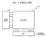
- FIG. 1is a block diagram of a conventional CIS-type solid-state image-sensing device 100 that includes an active pixel sensor (APS) array 110 , a row driver 120 , and an analog-to-digital converter 130 .
- the row driver 120receives a control signal from a row decoder (not shown), and the analog-to-digital converter 130 receives a control signal from a column decoder (not shown).
- the solid-state image-sensing device 100further includes a controller (not shown) that generates addressing signals for controlling timing and selection of pixels for outputting sensed image signals.
- a respective color filteris disposed on top of each pixel of the APS array 110 .
- the most common color filter arrayhas a Bayer color pattern in which filters of the colors red (R) and green (G) are alternately disposed on one row and in which filters of the colors G and blue (B) are alternately disposed on the next row.
- RGBred
- Ggreen
- Bblue
- the APS array 110includes over a million pixels for example.
- each pixel in the APS array 110generates a respective image signal by sensing light of the respective color filter with a respective photodiode and converting such light into a respective electrical signal.
- the respective image signal output from each pixel of the APS array 110is an analog signal of one of three colors, R, G, and B.
- the analog-to-digital converter 130converts such an analog image signal into a digital signal.
- the analog-to-digital converter 130uses a correlated double sampling (CDS) method to further process the image signals from the APS array 110 .
- CDScorrelated double sampling
- Such a methodis described, for example, in U.S. Pat. Nos. 5,982,318 and 6,067,113.
- the analog-to-digital conversionis basically divided into two operations: receiving a reset signal and the image signals from the APS array 110 , and then processing the reset signal and the image signals to generate digital signals representing the image sensed by the APS array 110 .
- the analog-to-digital converter 130subtracts the reset signal from the image signals before conversion into the digital signals.
- Such digital signalsare output to a digital signal processor that may further interpolate the digital image signals.
- the digital signal processorgenerates driving signals appropriate for the resolution of a display device such as a LCD (liquid crystal display).
- the image signalsare output with lowered resolution.
- the APS array 110having super extended graphics adapter (SXGA) resolution (1280 ⁇ 1024)
- regular image signalsare output at the SXGA resolution.
- image signalsare output at a video graphics adapter (VGA) resolution (640 ⁇ 480).
- VGAvideo graphics adapter
- UXGAultra extended graphics adaptor
- image signals of only a specific row and column that are spaced at a predetermined distanceare output to the analog-to-digital converter 130 for lowering the resolution.
- the image signal from one pixelis selected from among a 2 ⁇ 2 matrix of four pixels for the 1 ⁇ 2 resolution.
- the image signals from the other non-selected pixelsare ignored for reduced data processing. With such ignored image signals, a diagonal portion on the display image is not smoothly connected, resulting in aliasing noise that is displayed in a zigzag form.
- an image-sensing device of the present inventionprocesses the image signals from the array of pixels in the sub-sampling mode without ignoring such a substantial portion of the image signals.
- an image-sensing deviceincludes an array of pixels arranged in rows and columns.
- the image-sensing deviceincludes a driver that controls the array of pixels to output a combined image signal that is a combination of at least two image signals for at least two aligned pixels of at least two columns or rows having a substantially same color pattern.
- the combined image signalis an average of N image signals for a set of N aligned pixels in N consecutive odd or even rows having a substantially same color pattern.
- a set of N select transistors corresponding to the N aligned pixelsare turned on by the driver for generating the combined signal at a common node of the N select transistors.
- the drivercontrols the array to generate a respective combined image signal for a respective set of N aligned pixels at each column for the N consecutive odd or even rows.
- the image-sensing deviceincludes an analog mixing circuit that further averages the respective combined signals for M consecutive odd or even columns.
- the image-sensing deviceincludes an ADC (analog to digital converter) for converting each combined image signal as an analog signal into a digital signal.
- ADCanalog to digital converter
- a digital mixing circuitfurther averages the respective combined signals for M consecutive odd or even columns after the respective combined signals are each converted into a respective digital signal.
- the present inventionis used to particular advantage when the array of pixels has a Bayer color pattern such that the N image signals for the N aligned pixels are for a same color.
- the combined signal from the N image signalsis generated during a sub-sampling mode.
- FIG. 1shows a block diagram of a CIS-type solid-state image-sensing device, according to the prior art
- FIG. 2shows a block diagram of a CIS-type solid-state image-sensing device with an analog mixing circuit, according to an embodiment of the present invention
- FIG. 3shows a flow chart of steps during operation of the solid-state image-sensing device of FIG. 2 , according to an embodiment of the present invention
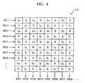
- FIG. 4shows an example color pattern for an active pixel sensor (APS) array of pixels of FIG. 2 ;
- APSactive pixel sensor
- FIG. 5shows circuit elements of two selected pixels having image signals that are combined, according to an embodiment of the present invention
- FIG. 6shows timing diagrams of a reset control signal and a transmission control signal applied on each pixel of FIG. 5 , according to an embodiment of the present invention.
- FIG. 7is a block diagram of a CIS-type solid-state image-sensing device with a digital mixing circuit, according to another embodiment of the present invention.
- FIGS. 1 , 2 , 3 , 4 , 5 , 6 , and 7refer to elements having similar structure and/or function.
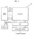
- FIG. 2shows a block diagram of a complimentary metal-oxide semiconductor (CMOS) image sensor (CIS)-type solid-state image-sensing device 200 according to an embodiment of the present invention.
- the CIS-type solid-state image-sensing device 200includes an active pixel sensor (APS) array 210 , a row driver 220 , an analog mixing circuit 230 , an analog-to-digital converter 240 , and a controller 250 .
- CMOScomplimentary metal-oxide semiconductor
- CIScomplimentary metal-oxide semiconductor
- CIS-type solid-state image-sensing device 200includes an active pixel sensor (APS) array 210 , a row driver 220 , an analog mixing circuit 230 , an analog-to-digital converter 240 , and a controller 250 .
- APSactive pixel sensor
- the CIS-type solid-state image-sensing device 200may be mounted within a small portable device such as a camera of a mobile phone or a digital still camera.
- the solid-state image-sensing device 200senses light for an image using photodiodes PD and converts the sensed light into electrical signals.
- the APS array 210is comprised of a two-dimensional matrix of pixels arranged in rows and columns. Each pixel has a respective photodiode PD for sensing light at a respective location in the APS array 210 to generate a respective image signal.
- the row driver 220generates a transmission control signal TX, a reset control signal RX, and a row selection signal SEL for controlling output of the image signals from the APS array 210 .
- the image-sensing device 200generates the three color signals (red (R), green (G), and blue (B)) representing an image, and such color signals are interpolated in an image signal processor for being displayed on a display device such as a liquid crystal display (LCD).
- a display devicesuch as a liquid crystal display (LCD).
- three color signals (R, Gr/Gb, and B) in converted formare used.
- the Gr and Gb signalsare interpolated using second and third color signals (B and R) that are next to a first color signal G in order to compensate for effects of consecutive color signals (R and B) (see FIG. 4 ).
- the pixels of the APS array 210are arranged in a Bayer color pattern.
- the present inventionmay be practiced for other color filter patterns.
- the controller 250sends a control signal indicating that the image-sensing device 200 is to operate in the sub-sampling mode.
- image signals with lower resolution than the resolution of the pixels in the APS array 210are output from the image-sensing device 200 .
- FIG. 3is a flow chart of steps for operation of the image-sensing device 200 of FIG. 2 .
- sub-sampling mode with 1 ⁇ 2 resolutionis described as an example.
- signal charges corresponding to an imageare accumulated in the photodiodes PD within the APS array 210 for a predetermined time when a mechanical shutter is opened (step S 310 of FIG. 3 ).
- the amount of signal charge accumulated in the photodiodes PDis determined by a transmission control signal TX from the row driver 220 .
- the APS array 210generates a reset signal VRST in response to the reset control signal RX while the signal charge is being accumulated in the photodiodes PD (step S 320 of FIG. 3 ). Moreover, the APS array 210 outputs image signals converted into photoelectrical signals by the photodiodes PD in response to the transmission control signal TX (step S 320 of FIG. 3 ). For the sub-sampling mode, the APS array 210 first averages two image signals from two pixels aligned along a same column for two consecutive odd or even rows to generate a row of combined image signals (step S 320 of FIG. 3 ).
- FIG. 4shows the Bayer pattern of the color filters disposed on the APS array 210 of FIG. 2 .
- Each pixel on the APS array 210has a respective color filter for a respective one of the three color signals (R, G, and B).
- the green filter Gwhich is closely related to the luminance signal, is disposed on all rows.
- the red filter R and the blue filter Bare alternately arranged as illustrated in FIG. 4 for each row to increase the brightness resolution.
- Gbdenotes a first green signal
- Grdenotes a second green signal
- both green signals Gb and Grbeing generated by an interpolation process in a signal processor disposed after the analog-to-digital converter 240 of FIG. 2 .
- the green signals Gb and Grare described as the green color signal G.
- the row selection signal SEL, the transmission control signal TX, and the reset control signal RXare generated from the row driver 220 and inputted to each pixel of the APS array 210 .
- FIG. 5shows circuit elements within two aligned pixels generating image signals that are averaged to generate a combined image signal in the sub-sampling mode.
- two aligned pixels 211 and 212are located in a same column of two consecutive odd rows, e.g., the first and third rows, respectively.
- the row driver 220generates a first row selection signal SEL 1 and a third row selection signal SEL 3 that are activated for such first and third rows.
- the two pixels 211 and 212are coupled at a common node that generates a reset signal VRST or the combined image signal VFD 1 .
- a common nodeis coupled to a drain terminal of a metal-oxide semiconductor field-effect transistor (MOSFET) M 9 .
- a bias voltage VBIASis applied on such a MOSFET M 9 for forming a bias circuit.
- the pixel 211is comprised of four MOSFETs M 1 , M 2 , M 3 , and M 4
- the pixel 212is comprised of four MOSFETs M 5 , M 6 , M 7 , and M 8 .
- the reset signal VRSTis output when the reset control signal RX is activated with turning on of the MOSFETs M 2 , M 3 , M 1 , M 6 , M 7 , and M 5 .
- odd rowssuch as rows corresponding to the select signals SEL 1 , SEL 3 , SEL 5 , . . . have a same color pattern.
- pixels aligned along a same column in such odd rowshave a color filter of a same color.
- even rowssuch as rows corresponding to the select signals SEL 2 , SEL 4 , SEL 6 , . . . have a same color pattern.
- pixels aligned along a same column in such even rowshave a color filter of a same color.
- the APS array 210generates a respective combined image signal from averaging the respective N image signals from a set of N pixels aligned along a same column for N odd rows when the respective select signals SEL 1 , SEL 3 , SEL 5 , . . . SELN and the transmission control signal TX are activated high, with N being at least two (step S 320 of FIG. 3 ).
- the reset signal VRSTis output for such a set of N aligned pixels when the reset control signal RX is activated instead (step 320 of FIG. 3 ).
- the APS array 210generates a respective combined signal for a respective set of N aligned pixels along each column in the N odd rows (step 320 of FIG. 3 ), to result in a row of combined signals VFD 1 , VFD 2 , VFD 3 , VFD 4 , VFD 5 , VFD 6 , VFD 7 , VFD 8 , . . . . Because the N odd rows have a same color pattern, the N aligned pixels along each column of such N odd rows have a color filter of a same color.
- the APS array 210generates a respective combined image signal from averaging the respective N image signals from a set of N pixels aligned along a same column for N even rows when the respective select signals SEL 2 , SEL 4 , SEL 6 , . . . SELN and the transmission control signal TX are activated high, with N being at least two (step S 330 of FIG. 3 ).
- the reset signal VRSTis output for such a set of N aligned pixels when the reset control signal RX is activated instead (step 330 of FIG. 3 ).
- the APS array 210generates a respective combined signal for a respective set of N aligned pixels along each column in the N even rows (step 330 of FIG. 3 ), to result in a row of combined signals VFD 1 , VFD 2 , VFD 3 , VFD 4 , VFD 5 , VFD 6 , VFD 7 , VFD 8 , . . . . Because the N even rows have a same color pattern, the N aligned pixels along each column of such N even row have a color filter of a same color. Such a process of combining the N image signals from the N aligned pixels for the N consecutive odd or even rows is repeated for each set of N consecutive odd or even rows for the whole APS array 210 (step S 340 of FIG. 3 ).
- the analog mixing circuit 230 of FIG. 2further averages the row of resulting combined signals in the horizontal direction. For example, the analog mixing circuit 230 averages the combined signals of M consecutive odd or even columns corresponding to the same color within the row of combined signals VFD 1 , VFD 2 , VFD 3 , VFD 4 , VFD 5 , VFD 6 , VFD 7 , VFD 8 , . . . .
- the horizontal resolutionis reduced by a factor of 1/M in the sub-sampling mode.
- the analog mixing circuit 230averages two consecutive odd combined image signals VFD 1 and VFD 3 (which are analog signals) and outputs such a further averaged signal as further combined signals VFD 1 and VFD 3 (which are now the same further averaged signal) to the analog-to-digital converter 240 .
- the analog mixing circuit 230averages two consecutive even combined image signals VFD 2 and VFD 4 (which are analog signals) and outputs such a further averaged signal as further combined signals VFD 2 and VFD 4 (which are now the same further averaged signal) to the analog-to-digital converter 240 .
- the analog-to-digital converter 240then calculates a difference between each of the further averaged signals from the analog mixing circuit 230 and the reset signal VRST and converts such a difference that is an analog signal into a digital signal.
- a signal processorreceives the respective digital signal generated for each of the further combined signals VFD 1 , VFD 2 , VFD 3 , VFD 4 , VFD 5 , VFD 6 , VFD 7 , VFD 8 , . . . .
- Such a signal processorselects just one of the same digital signals occurring in the M consecutive odd or even columns for further processing.
- Steps S 310 , S 320 , S 330 , and S 340 of FIG. 3are repeated for each one-frame unit that displays one image on a display device.
- a sub-sampling mode with the 1 ⁇ 2 resolutionhas been described as an example, the present invention may be practiced for 1 ⁇ 3, 1 ⁇ 4, or 1 ⁇ 5 resolution when N and M in the above description are 3, 4, or 5, respectively.
- the sub-sampling mode with the 1 ⁇ 2 resolutionadvantageously has less circuit complexity.
- FIG. 7is a block diagram of a CIS-type solid-state image-sensing device 700 according to another embodiment of the present invention.
- the CIS-type solid-state image-sensing device 700includes an APS array 710 , a row driver 720 , an analog-to-digital converter 730 , a digital mixing circuit 740 , and a controller 750 .
- the structure and operation of the APS array 710 , the row driver 720 , and the controller 750are similar to the structure and operation of the APS array 210 , the row driver 220 , and the controller 250 of FIG. 2 , to generate the combined signals VFD 1 , VFD 2 , VFD 3 , VFD 4 , VFD 5 , VFD 6 , VFD 7 , VFD 8 , . . . .
- the analog-to-digital converter 730calculates a difference between such combined signals and the reset signal VRST which are analog signals. In addition, the analog-to-digital converter 730 converts such a difference into a digital signal for each of the combined signals VFD 1 , VFD 2 , VFD 3 , VFD 4 , VFD 5 , VFD 6 , VFD 7 , VFD 8 , . . . .
- the digital mixing circuit 740further averages the row of resulting digital signals from the analog-to-digital converter 730 in the horizontal direction. For example, the digital mixing circuit 740 averages the digital signals of M consecutive odd or even columns corresponding to the same color within the row of digital signals from the analog-to-digital converter 730 . Thus, the horizontal resolution is reduced by a factor of 1/M in the sub-sampling mode.
- a signal processorselects just one of the same digital signals occurring in the M consecutive odd or even columns that have been averaged for further processing.
- the image signals from substantially all of the pixels of the APS array 210 of FIG. 2 or 710 of FIG. 7are used for generating the combined image signals with lower resolution in the sub-sampling mode.
- the sensed imageis displayed with higher quality in such a sub-sampling mode.
- Such higher display qualityis especially advantageous when the image-sensing device 200 or 700 is formed within small portable electronic devices such as a camera of a mobile phone or a digital still camera.
Landscapes
- Engineering & Computer Science (AREA)
- Multimedia (AREA)
- Signal Processing (AREA)
- Chemical & Material Sciences (AREA)
- Combustion & Propulsion (AREA)
- Transportation (AREA)
- Mechanical Engineering (AREA)
- Color Television Image Signal Generators (AREA)
- Transforming Light Signals Into Electric Signals (AREA)
Abstract
Description
Claims (18)
Applications Claiming Priority (3)
| Application Number | Priority Date | Filing Date | Title |
|---|---|---|---|
| KR2004-8926 | 2004-02-11 | ||
| KR1020040008926AKR100871687B1 (en) | 2004-02-11 | 2004-02-11 | Solid state image pickup device with improved display quality in subsampling mode and its driving method |
| KR10-2004-0008926 | 2004-02-11 |
Publications (2)
| Publication Number | Publication Date |
|---|---|
| US20050174454A1 US20050174454A1 (en) | 2005-08-11 |
| US7724294B2true US7724294B2 (en) | 2010-05-25 |
Family
ID=34825165
Family Applications (1)
| Application Number | Title | Priority Date | Filing Date |
|---|---|---|---|
| US11/035,007Active2027-10-13US7724294B2 (en) | 2004-02-11 | 2005-01-12 | Sub-sampling with higher display quality in image-sensing device |
Country Status (4)
| Country | Link |
|---|---|
| US (1) | US7724294B2 (en) |
| JP (1) | JP2005229603A (en) |
| KR (1) | KR100871687B1 (en) |
| CN (1) | CN100527780C (en) |
Cited By (3)
| Publication number | Priority date | Publication date | Assignee | Title |
|---|---|---|---|---|
| US20090309991A1 (en)* | 2008-06-11 | 2009-12-17 | Yong Lim | Pseudo-digital average sub sampling method and apparatus |
| TWI484816B (en)* | 2011-07-04 | 2015-05-11 | Mstar Semiconductor Inc | Passive 3d image system and image processing method thereof |
| US9380233B2 (en) | 2013-02-27 | 2016-06-28 | Samsung Electronics Co., Ltd. | Image sensor |
Families Citing this family (8)
| Publication number | Priority date | Publication date | Assignee | Title |
|---|---|---|---|---|
| KR100674957B1 (en)* | 2005-02-23 | 2007-01-26 | 삼성전자주식회사 | Solid-state imaging device and driving method thereof for averaging and sub-sampling analog signals at arbitrary sub-sampling rate |
| US20070201058A1 (en)* | 2006-02-28 | 2007-08-30 | Texas Instruments Incorporated | Systems and methods for indirect image data conversion |
| JP5253956B2 (en)* | 2008-10-16 | 2013-07-31 | シャープ株式会社 | Solid-state imaging device, driving method thereof, and electronic information device |
| KR101623591B1 (en) | 2009-11-24 | 2016-05-23 | 삼성전자주식회사 | Apparatus and method for improving quality of preview image |
| KR101643773B1 (en)* | 2009-12-03 | 2016-07-28 | 삼성전자주식회사 | Apparatus and method for improving quality of preview image |
| HUE039688T2 (en)* | 2010-06-01 | 2019-01-28 | Boly Media Comm Shenzhen Co | Multispectral photoreceptive device and sampling method thereof |
| KR20210037302A (en) | 2019-09-27 | 2021-04-06 | 삼성전자주식회사 | Image sensor, and operation method thereof |
| CN118967485B (en)* | 2024-10-16 | 2024-12-31 | 大连创锐光谱科技有限公司 | High-speed area-array camera image processing method and high-speed area-array camera |
Citations (22)
| Publication number | Priority date | Publication date | Assignee | Title |
|---|---|---|---|---|
| US5982318A (en) | 1997-10-10 | 1999-11-09 | Lucent Technologies Inc. | Linearizing offset cancelling white balancing and gamma correcting analog to digital converter for active pixel sensor imagers with self calibrating and self adjusting properties |
| US6061093A (en)* | 1994-02-21 | 2000-05-09 | Sony Corporation | Solid-state imager having capacitors connected to vertical signal lines and a charge detection circuit |
| US6067113A (en)* | 1996-09-12 | 2000-05-23 | Vsli Vision Limited | Offset noise cancellation in array image sensors |
| US20010010554A1 (en)* | 2000-01-31 | 2001-08-02 | Olympus Optical Co. Ltd. | Imaging apparatus capable of adding together signal charges from pixels and reading out the added pixel signals |
| US6437307B1 (en)* | 1997-09-12 | 2002-08-20 | Fraunhofer-Gesellschaft Zur Forderung Zur Angewandten Forshung E.V. | Image detection member and assembly of image detection members |
| US6507011B2 (en)* | 1998-02-19 | 2003-01-14 | Micron Technology, Inc. | Active pixel color linear sensor with line-packed pixel readout |
| US20040100436A1 (en)* | 2002-11-22 | 2004-05-27 | Sharp Kabushiki Kaisha | Shift register block, and data signal line driving circuit and display device using the same |
| US20040141079A1 (en)* | 2003-01-10 | 2004-07-22 | Matsushita Electric Industrial Co., Ltd. | Solid-state imaging device and camera using the same |
| US6807319B2 (en)* | 2000-06-12 | 2004-10-19 | Sharp Laboratories Of America, Inc. | Methods and systems for improving display resolution in achromatic images using sub-pixel sampling and visual error filtering |
| US6842192B1 (en)* | 1997-09-26 | 2005-01-11 | Sony Corporation | Solid state image pickup device having an amplifier for each vertical signal line and driving method therefor |
| US20050012836A1 (en)* | 2003-07-15 | 2005-01-20 | Eastman Kodak Company | Image sensor with charge binning and dual channel readout |
| US6888568B1 (en)* | 1999-08-19 | 2005-05-03 | Dialog Semiconductor Gmbh | Method and apparatus for controlling pixel sensor elements |
| US20050151866A1 (en)* | 2004-01-13 | 2005-07-14 | Haruhisa Ando | Wide dynamic range operations for imaging |
| US6956605B1 (en)* | 1998-08-05 | 2005-10-18 | Canon Kabushiki Kaisha | Image pickup apparatus |
| US6999120B1 (en)* | 1999-10-07 | 2006-02-14 | Kabushiki Kaisha Toshiba | CMOS imaging device for amplifying and fetching signal charge |
| US7002713B2 (en)* | 2000-07-27 | 2006-02-21 | Canon Kabushiki Kaisha | Image processing apparatus |
| US7092017B2 (en)* | 2002-09-13 | 2006-08-15 | Eastman Kodak Company | Fixed pattern noise removal in CMOS imagers across various operational conditions |
| US7129979B1 (en)* | 2000-04-28 | 2006-10-31 | Eastman Kodak Company | Image sensor pixel for global electronic shuttering |
| US7129978B1 (en)* | 1998-07-13 | 2006-10-31 | Zoran Corporation | Method and architecture for an improved CMOS color image sensor |
| US7154545B2 (en)* | 2001-04-30 | 2006-12-26 | Hewlett-Packard Development Company, L.P. | Image scanner photosensor assembly with improved spectral accuracy and increased bit-depth |
| US7283167B1 (en)* | 2000-03-01 | 2007-10-16 | Thomson Licensing Sas | Method and device for reading out image data of a sub-range of an image |
| US7372490B2 (en)* | 1999-03-08 | 2008-05-13 | Micron Technology, Inc. | Multi junction APS with dual simultaneous integration |
Family Cites Families (11)
| Publication number | Priority date | Publication date | Assignee | Title |
|---|---|---|---|---|
| JPH0720248B2 (en)* | 1987-06-09 | 1995-03-06 | 富士写真フイルム株式会社 | Filter color allocation method for solid-state image sensor |
| JP3862298B2 (en)* | 1994-12-22 | 2006-12-27 | キヤノン株式会社 | Photoelectric conversion device |
| JP3897389B2 (en)* | 1996-02-22 | 2007-03-22 | キヤノン株式会社 | Photoelectric conversion device driving method and photoelectric conversion device |
| US6721008B2 (en)* | 1998-01-22 | 2004-04-13 | Eastman Kodak Company | Integrated CMOS active pixel digital camera |
| JPWO2003034714A1 (en)* | 2001-10-15 | 2005-02-10 | 株式会社ニコン | Solid-state imaging device |
| JP2005109968A (en)* | 2003-09-30 | 2005-04-21 | Matsushita Electric Ind Co Ltd | Color solid-state imaging device |
| KR100640603B1 (en)* | 2004-06-22 | 2006-11-01 | 삼성전자주식회사 | Improved solid state image sensing device and driving method for averaging sub-sampled analog signals |
| KR100994993B1 (en)* | 2004-03-16 | 2010-11-18 | 삼성전자주식회사 | Solid-state image sensor and driving method thereof for outputting video signal obtained by averaging subsampled analog signal |
| KR100674957B1 (en)* | 2005-02-23 | 2007-01-26 | 삼성전자주식회사 | Solid-state imaging device and driving method thereof for averaging and sub-sampling analog signals at arbitrary sub-sampling rate |
| KR100674963B1 (en)* | 2005-03-09 | 2007-01-26 | 삼성전자주식회사 | Solid-State Imaging Device and Method Supporting Subsampling Using the Inter-Column Analog Signal Sum |
| KR100716736B1 (en)* | 2005-05-18 | 2007-05-14 | 삼성전자주식회사 | Column Analog-to-Digital Converter Apparatus and Method Supporting High Frame Rate in Subsampling Mode |
- 2004
- 2004-02-11KRKR1020040008926Apatent/KR100871687B1/ennot_activeExpired - Fee Related
- 2005
- 2005-01-12USUS11/035,007patent/US7724294B2/enactiveActive
- 2005-02-07JPJP2005031160Apatent/JP2005229603A/enactivePending
- 2005-02-08CNCNB2005100716760Apatent/CN100527780C/ennot_activeExpired - Lifetime
Patent Citations (22)
| Publication number | Priority date | Publication date | Assignee | Title |
|---|---|---|---|---|
| US6061093A (en)* | 1994-02-21 | 2000-05-09 | Sony Corporation | Solid-state imager having capacitors connected to vertical signal lines and a charge detection circuit |
| US6067113A (en)* | 1996-09-12 | 2000-05-23 | Vsli Vision Limited | Offset noise cancellation in array image sensors |
| US6437307B1 (en)* | 1997-09-12 | 2002-08-20 | Fraunhofer-Gesellschaft Zur Forderung Zur Angewandten Forshung E.V. | Image detection member and assembly of image detection members |
| US6842192B1 (en)* | 1997-09-26 | 2005-01-11 | Sony Corporation | Solid state image pickup device having an amplifier for each vertical signal line and driving method therefor |
| US5982318A (en) | 1997-10-10 | 1999-11-09 | Lucent Technologies Inc. | Linearizing offset cancelling white balancing and gamma correcting analog to digital converter for active pixel sensor imagers with self calibrating and self adjusting properties |
| US6507011B2 (en)* | 1998-02-19 | 2003-01-14 | Micron Technology, Inc. | Active pixel color linear sensor with line-packed pixel readout |
| US7129978B1 (en)* | 1998-07-13 | 2006-10-31 | Zoran Corporation | Method and architecture for an improved CMOS color image sensor |
| US6956605B1 (en)* | 1998-08-05 | 2005-10-18 | Canon Kabushiki Kaisha | Image pickup apparatus |
| US7372490B2 (en)* | 1999-03-08 | 2008-05-13 | Micron Technology, Inc. | Multi junction APS with dual simultaneous integration |
| US6888568B1 (en)* | 1999-08-19 | 2005-05-03 | Dialog Semiconductor Gmbh | Method and apparatus for controlling pixel sensor elements |
| US6999120B1 (en)* | 1999-10-07 | 2006-02-14 | Kabushiki Kaisha Toshiba | CMOS imaging device for amplifying and fetching signal charge |
| US20010010554A1 (en)* | 2000-01-31 | 2001-08-02 | Olympus Optical Co. Ltd. | Imaging apparatus capable of adding together signal charges from pixels and reading out the added pixel signals |
| US7283167B1 (en)* | 2000-03-01 | 2007-10-16 | Thomson Licensing Sas | Method and device for reading out image data of a sub-range of an image |
| US7129979B1 (en)* | 2000-04-28 | 2006-10-31 | Eastman Kodak Company | Image sensor pixel for global electronic shuttering |
| US6807319B2 (en)* | 2000-06-12 | 2004-10-19 | Sharp Laboratories Of America, Inc. | Methods and systems for improving display resolution in achromatic images using sub-pixel sampling and visual error filtering |
| US7002713B2 (en)* | 2000-07-27 | 2006-02-21 | Canon Kabushiki Kaisha | Image processing apparatus |
| US7154545B2 (en)* | 2001-04-30 | 2006-12-26 | Hewlett-Packard Development Company, L.P. | Image scanner photosensor assembly with improved spectral accuracy and increased bit-depth |
| US7092017B2 (en)* | 2002-09-13 | 2006-08-15 | Eastman Kodak Company | Fixed pattern noise removal in CMOS imagers across various operational conditions |
| US20040100436A1 (en)* | 2002-11-22 | 2004-05-27 | Sharp Kabushiki Kaisha | Shift register block, and data signal line driving circuit and display device using the same |
| US20040141079A1 (en)* | 2003-01-10 | 2004-07-22 | Matsushita Electric Industrial Co., Ltd. | Solid-state imaging device and camera using the same |
| US20050012836A1 (en)* | 2003-07-15 | 2005-01-20 | Eastman Kodak Company | Image sensor with charge binning and dual channel readout |
| US20050151866A1 (en)* | 2004-01-13 | 2005-07-14 | Haruhisa Ando | Wide dynamic range operations for imaging |
Non-Patent Citations (3)
| Title |
|---|
| Japanese Patent No. JP2002142155 to Takashi et al., having Publication date of May 17, 2002 (w/ English Abstract page). |
| Japanese Patent No. JP2003046876 to Hidetoshi, having Publication date of Feb. 5, 2003 (w/ English Abstract page). |
| Korean Patent Application No. 1020010044098 to Meados, having Publication date of Feb. 1, 2002 (w/ English Abstract page). |
Cited By (6)
| Publication number | Priority date | Publication date | Assignee | Title |
|---|---|---|---|---|
| US20090309991A1 (en)* | 2008-06-11 | 2009-12-17 | Yong Lim | Pseudo-digital average sub sampling method and apparatus |
| US8149289B2 (en)* | 2008-06-11 | 2012-04-03 | Samsung Electronics Co., Ltd. | Pseudo-digital average sub sampling method and apparatus |
| US8754956B2 (en) | 2008-06-11 | 2014-06-17 | Samsung Electronics Co., Ltd. | Pseudo-digital average sub sampling method and apparatus |
| TWI484816B (en)* | 2011-07-04 | 2015-05-11 | Mstar Semiconductor Inc | Passive 3d image system and image processing method thereof |
| US9215437B2 (en) | 2011-07-04 | 2015-12-15 | Mstar Semiconductor, Inc. | Passive 3D image system and image processing method thereof |
| US9380233B2 (en) | 2013-02-27 | 2016-06-28 | Samsung Electronics Co., Ltd. | Image sensor |
Also Published As
| Publication number | Publication date |
|---|---|
| KR20050080814A (en) | 2005-08-18 |
| US20050174454A1 (en) | 2005-08-11 |
| CN1717003A (en) | 2006-01-04 |
| JP2005229603A (en) | 2005-08-25 |
| KR100871687B1 (en) | 2008-12-05 |
| CN100527780C (en) | 2009-08-12 |
Similar Documents
| Publication | Publication Date | Title |
|---|---|---|
| US7193199B2 (en) | Solid-state image-sensing device that compensates for brightness at edges of a display area and a driving method thereof | |
| KR100660866B1 (en) | Pixel Circuit and Method for Low Noise Global Shutter Operation in Image Sensors | |
| US9942482B2 (en) | Image sensor with transfer gate control signal lines | |
| US8023018B2 (en) | Drive method for solid-state imaging device, solid-state imaging device, and imaging apparatus | |
| US7319218B2 (en) | Method and apparatus for pixel signal binning and interpolation in column circuits of a sensor circuit | |
| US8199237B2 (en) | Imaging device, control method therefor, and camera | |
| CN1838741B (en) | Solid state image sensing device and method for subsampling using inter-column analog domain signal summation | |
| US7521659B2 (en) | Driving an image sensor with reduced area and high image quality | |
| US20080218598A1 (en) | Imaging method, imaging apparatus, and driving device | |
| KR100660865B1 (en) | Pixel circuit and driving method with shared wiring / transistor in image sensor | |
| JP4501350B2 (en) | Solid-state imaging device and imaging device | |
| KR20050092579A (en) | Solid state image sensing device and driving method thereof outputting digital image signals of averaged sub-sampled analog signals | |
| KR20100066396A (en) | Solid-state imaging device, method for processing signal of solid-state imaging device, and imaging apparatus | |
| JP2010161484A (en) | Solid-state imaging apparatus, method for processing signal of solid-state imaging apparatus, and imaging apparatus | |
| KR20150013454A (en) | Imaging device and imaging method, electronic apparatus, as well as program | |
| US7623175B2 (en) | Solid state image sensing device for analog-averaging and sub-sampling of image signals at a variable sub-sampling rate and method of driving the same | |
| US7724294B2 (en) | Sub-sampling with higher display quality in image-sensing device | |
| JP2000341699A (en) | Color imaging apparatus and imaging system using the same | |
| US7492403B2 (en) | Solid state image sensing device and driving method with sub-sampling mode and improved dynamic range | |
| WO2013100097A1 (en) | Imaging device, control method for imaging device, and control program | |
| JP2009130574A (en) | Imaging apparatus and solid-state imaging device driving method | |
| JP2000013809A (en) | Imaging display device |
Legal Events
| Date | Code | Title | Description |
|---|---|---|---|
| AS | Assignment | Owner name:SAMSUNG ELECTRONICS CO., LTD., KOREA, REPUBLIC OF Free format text:ASSIGNMENT OF ASSIGNORS INTEREST;ASSIGNORS:AHN, JUNG-CHAK;LIM, SU-HUN;REEL/FRAME:016177/0394 Effective date:20041229 Owner name:SAMSUNG ELECTRONICS CO., LTD.,KOREA, REPUBLIC OF Free format text:ASSIGNMENT OF ASSIGNORS INTEREST;ASSIGNORS:AHN, JUNG-CHAK;LIM, SU-HUN;REEL/FRAME:016177/0394 Effective date:20041229 | |
| AS | Assignment | Owner name:MICROSOFT CORPORATION,WASHINGTON Free format text:ASSIGNMENT OF ASSIGNORS INTEREST;ASSIGNORS:BURST, ALEXANDRU D.;SOL, ALISSON A.S.;KORONTHALY, DAVID;AND OTHERS;REEL/FRAME:016100/0559 Effective date:20050523 Owner name:MICROSOFT CORPORATION, WASHINGTON Free format text:ASSIGNMENT OF ASSIGNORS INTEREST;ASSIGNORS:BURST, ALEXANDRU D.;SOL, ALISSON A.S.;KORONTHALY, DAVID;AND OTHERS;REEL/FRAME:016100/0559 Effective date:20050523 | |
| STCF | Information on status: patent grant | Free format text:PATENTED CASE | |
| FPAY | Fee payment | Year of fee payment:4 | |
| MAFP | Maintenance fee payment | Free format text:PAYMENT OF MAINTENANCE FEE, 8TH YEAR, LARGE ENTITY (ORIGINAL EVENT CODE: M1552) Year of fee payment:8 | |
| MAFP | Maintenance fee payment | Free format text:PAYMENT OF MAINTENANCE FEE, 12TH YEAR, LARGE ENTITY (ORIGINAL EVENT CODE: M1553); ENTITY STATUS OF PATENT OWNER: LARGE ENTITY Year of fee payment:12 |