US7724284B2 - Multi-camera system and method having a common processing block - Google Patents
Multi-camera system and method having a common processing blockDownload PDFInfo
- Publication number
- US7724284B2 US7724284B2US11/238,461US23846105AUS7724284B2US 7724284 B2US7724284 B2US 7724284B2US 23846105 AUS23846105 AUS 23846105AUS 7724284 B2US7724284 B2US 7724284B2
- Authority
- US
- United States
- Prior art keywords
- image
- image data
- capture device
- camera
- capturing
- Prior art date
- Legal status (The legal status is an assumption and is not a legal conclusion. Google has not performed a legal analysis and makes no representation as to the accuracy of the status listed.)
- Active, expires
Links
Images


Classifications
- H—ELECTRICITY
- H04—ELECTRIC COMMUNICATION TECHNIQUE
- H04N—PICTORIAL COMMUNICATION, e.g. TELEVISION
- H04N1/00—Scanning, transmission or reproduction of documents or the like, e.g. facsimile transmission; Details thereof
- H04N1/00127—Connection or combination of a still picture apparatus with another apparatus, e.g. for storage, processing or transmission of still picture signals or of information associated with a still picture
- H04N1/00281—Connection or combination of a still picture apparatus with another apparatus, e.g. for storage, processing or transmission of still picture signals or of information associated with a still picture with a telecommunication apparatus, e.g. a switched network of teleprinters for the distribution of text-based information, a selective call terminal
- H04N1/00307—Connection or combination of a still picture apparatus with another apparatus, e.g. for storage, processing or transmission of still picture signals or of information associated with a still picture with a telecommunication apparatus, e.g. a switched network of teleprinters for the distribution of text-based information, a selective call terminal with a mobile telephone apparatus
- H—ELECTRICITY
- H04—ELECTRIC COMMUNICATION TECHNIQUE
- H04N—PICTORIAL COMMUNICATION, e.g. TELEVISION
- H04N23/00—Cameras or camera modules comprising electronic image sensors; Control thereof
- H04N23/45—Cameras or camera modules comprising electronic image sensors; Control thereof for generating image signals from two or more image sensors being of different type or operating in different modes, e.g. with a CMOS sensor for moving images in combination with a charge-coupled device [CCD] for still images
- H—ELECTRICITY
- H04—ELECTRIC COMMUNICATION TECHNIQUE
- H04N—PICTORIAL COMMUNICATION, e.g. TELEVISION
- H04N25/00—Circuitry of solid-state image sensors [SSIS]; Control thereof
- H04N25/70—SSIS architectures; Circuits associated therewith
- H04N25/76—Addressed sensors, e.g. MOS or CMOS sensors
- H—ELECTRICITY
- H04—ELECTRIC COMMUNICATION TECHNIQUE
- H04N—PICTORIAL COMMUNICATION, e.g. TELEVISION
- H04N1/00—Scanning, transmission or reproduction of documents or the like, e.g. facsimile transmission; Details thereof
- H04N1/00127—Connection or combination of a still picture apparatus with another apparatus, e.g. for storage, processing or transmission of still picture signals or of information associated with a still picture
- H04N1/00347—Connection or combination of a still picture apparatus with another apparatus, e.g. for storage, processing or transmission of still picture signals or of information associated with a still picture with another still picture apparatus, e.g. hybrid still picture apparatus
- H—ELECTRICITY
- H04—ELECTRIC COMMUNICATION TECHNIQUE
- H04N—PICTORIAL COMMUNICATION, e.g. TELEVISION
- H04N2101/00—Still video cameras
- H—ELECTRICITY
- H04—ELECTRIC COMMUNICATION TECHNIQUE
- H04N—PICTORIAL COMMUNICATION, e.g. TELEVISION
- H04N2201/00—Indexing scheme relating to scanning, transmission or reproduction of documents or the like, and to details thereof
- H04N2201/0008—Connection or combination of a still picture apparatus with another apparatus
- H04N2201/001—Sharing resources, e.g. processing power or memory, with a connected apparatus or enhancing the capability of the still picture apparatus
- H—ELECTRICITY
- H04—ELECTRIC COMMUNICATION TECHNIQUE
- H04N—PICTORIAL COMMUNICATION, e.g. TELEVISION
- H04N2201/00—Indexing scheme relating to scanning, transmission or reproduction of documents or the like, and to details thereof
- H04N2201/0008—Connection or combination of a still picture apparatus with another apparatus
- H04N2201/0063—Constructional details
- H—ELECTRICITY
- H04—ELECTRIC COMMUNICATION TECHNIQUE
- H04N—PICTORIAL COMMUNICATION, e.g. TELEVISION
- H04N2201/00—Indexing scheme relating to scanning, transmission or reproduction of documents or the like, and to details thereof
- H04N2201/0077—Types of the still picture apparatus
- H04N2201/0084—Digital still camera
Definitions
- Digital cameras and digital video camerasare becoming more prevalent in various electronic devices of today's electronics. It is common for cameras to be included in mobile phones, handheld devices, and portable/laptop computers. Because such digital cameras and digital video cameras are becoming cheaper to manufacture and are being realized in smaller packages, the demand for devices to include such cameras is increasing. As a result, more and more functionality for these cameras system is also being demanded.
- cameras that are mounted to laptop computers, mobile phones and the likehave typically been mounted in a fixed position such that any focal path of an optical train associated with the camera system was set relative to the device. That is, to point the camera in a different direction, the entire device needs to be maneuvered.
- a laptop computer having a camera pointing straight out of the view screenwould require a user to point the view screen at whatever the user wishes to capture as a picture or video.
- a laptop computer screenmay include a swivel-mounted camera at the top of the view screen that may be rotated as much as 180 degrees backwards to capture images on the opposite side of the view screen.
- maneuverable camerassolved the problem of not being able to see the view screen when taking pictures or capturing video, but introduced several new problems.
- Such new problemsinclude typical problems always associated with maneuverable devices requiring electronic connections inside the maneuverable part, such as flexible wiring and connection points. These flexible wiring accommodations are not only more expensive, but are far more prone to fail with far less use. Thus, even though maneuverable camera systems solved the original problem, the implementation and application left a lot to be desired.
- a device requiring more than a focal path for a camera in an opposite direction of a view screenmay be manufactured to have the camera system simply mounted to face the opposite direction.
- This solutionrestricted the camera use to subjects on the opposite side of the view screen.
- the usercould not simultaneously be captured by the camera and also view a feed on the view screen from somewhere else.
- FIG. 1shows a block diagram of a conventional camera system 100 having two distinct cameras that are pointed in opposite or relatively opposite optical directions.
- conventional camera systems having two camerasemploy two separate camera blocks.
- a first camera block 101includes a first optical train 105 situated to focus incident light upon a first sensor 110 .
- the first sensor 110typically includes a first pixel array 111 for capturing incident light in a known pixel-by-pixel manner.
- the optical informationmay then be sent to a processing block 130 for processing and storage.
- a second camera block 151is also included in the conventional multi-camera system 100 .
- the second camera block 151also includes an optical train 155 , a sensor 150 , a pixel array 151 and a processing block 180 that operate in conjunction with other similar to the first camera block 101 described above.
- the first camera block 101 and the second camera block 151are autonomous and do not in any manner interact with each other. In this sense, each camera block 101 and 151 is independent and typically disposed on separate integrated circuits (ICs) or separate electronic circuit boards (ECBs).
- each onerequires a specific amount of space, power, and cost in the overall system 100 implementation.
- each onerequires a specific amount of space, power, and cost in the overall system 100 implementation.
- having two cameras in the multi-camera system 100results in twice the cost, twice the implementation space and twice the power requirements over a system with only one camera.
- An embodiment of the inventionis directed to a multi-camera system having two optical paths with a single processing path for the two optical paths.
- a multi-camera systemtypically includes a first image-capture device associated with a first optical train wherein the first image-capture device is typically pointed in a first direction (i.e., away from the user).
- the multi-camera systemfurther includes a second image-capture device having a second optical train wherein the second image-capture device is typically pointed in a second direction (i.e., toward the user).
- the multi-camera systemfurther includes a single processing block coupled to the first image-capture device and the second image-capture device. The processing block is typically operable to process image data captured at each image-capture device.
- the two optical path/sensor assembliesi.e., cameras
- the two optical path/sensor assembliesmay be designed for specific purposes, such as a first camera for high-resolution image capture and a second camera for low-resolution video conferencing.
- FIG. 1is a block diagram of a conventional camera system having two distinct cameras that are pointed in opposite or relatively opposite optical directions;
- FIG. 2is a block diagram of a multi-camera system having two optical trains pointed in different direction in accordance with an embodiment of the invention.
- FIG. 3is a block diagram of a system having the multi-camera system of FIG. 2 disposed therein in accordance with an embodiment of the invention.
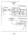
- FIG. 2is a block diagram of a multi-camera system 200 having two optical trains 205 and 255 pointed in different directions in accordance with an embodiment of the invention.
- a first sensor 210associated with a first optical train 205
- a second sensor 250associated with a second optical train 255
- the first sensor 210 and the processing block 230may comprise a first camera block 201 while the second sensor 251 may be part of a second camera block 251 .
- the distinctionis irrelevant and presented merely for the purposes of explanation and understanding.
- the first sensor 210typically includes a pixel array 211 situated to have incident light focused from the associated optical train 205 .
- the pixel array 211is further coupled to column amplifiers 212 for transducing the captured light into an analog signal for transmission to the processing block 230 .
- the sensor 210typically includes other circuitry but is not included or discussed herein for brevity.
- the optical train 205is typically pointed in a first direction such that one of the above-described scenarios may be accomplished. That is, the first optical train 205 may be included in the system 200 to provide a camera pointing away from the user of a laptop or mobile phone. In this manner, the first optical train 205 (together with the first sensor 210 ) may be used as a camera for taking pictures, capturing video and other camera functions wherein the camera typically points away from the user.
- the second sensor 250also includes a pixel array 251 situated to have incident light focused from the second associated optical train 255 .
- the pixel array 251is further coupled to column amplifiers 252 for similarly transducing the captured light into an analog signal for transmission to the processing block 230 .
- the second optical train 255is typically pointed in a second direction such that one of the other above-described scenarios may be accomplished. That is, the second optical train 255 may be included in the system 200 to provide a camera pointing toward the user of a laptop or mobile phone. In this manner, the second optical train 255 (together with the second sensor 250 ) may be used as a camera for video conferencing, capturing a second video feed and other camera functions wherein the camera typically points toward the user.
- Each sensor 210 and 250is electronically coupled to the processing block 230 such that analog signals representing captured light images may be transmitted to the processing block 230 .
- the second camera block 251i.e., the second sensor 250 and second optical train 251
- each sensor 210 and 250may produce analog signals representing captured image data for processing to the processing block 230 .
- the processing block 230may, in fact, be part of the other camera block 251 or its own separate block as the distinction in FIG. 2 is merely for illustrative purposes.
- the unity gain buffer 260may be integrated with any block.
- the processing block 230typically includes a processor 220 and a bus 219 .
- the processor 220typically controls a number of additional components through communications over the bus 219 .
- the analog signalis routed through a set of gain amplifiers 221 for amplifying the analog signal to a suitable level for further processing. Then the analog signal is passed through an analog-to-digital converter 222 (A/D) where the analog signal is converted into a digital signal.
- A/Danalog-to-digital converter
- the signalmay be further processed in several different known ways.
- the entire digital imagemay be processed to balance light and/or balance color.
- Spurious signalsmay be smoothed and other picture effects may be added.
- These image processing stepsare well known in the art and are generally represented in FIG. 2 as the image pipe 223 .
- the image pipe 223the image or portion thereof, undergoes any number of desired processing steps before being stored in a memory 224 .
- the processing block 230typically includes a set of user registers 226 for storing user-chosen parameters that may change by inputting values to the multi-camera system 200 .
- some processingmay be implemented via firmware 225 as some steps may be processing intensive and not subject to user parameter changes.
- the firmware 225is implemented to deal with processing parameters related to the size of each pixel array 211 and 251 .
- two optical trains 205 and 255 feeding analog signals into a single processing block 230is an efficient way of realizing a multi-camera system 200 .
- Such a system 200saves implementation space with having only one processing block 230 . Further, manufacturing costs are less with only one processing block 230 as two distinct processing blocks are not required. Further yet operational power is minimized with only one processing block 230 because only one processor 220 is required.
- realizing a multi-camera system 200 wherein two separate sensors 210 and 250 having respective optical trains 205 and 255 feeding into one processing block 230is a more efficient solution than conventional multi-camera systems of the past.
- the two camera blocks 201 and 251may be disposed on one or more ICs or ECBs.
- the first camera block 201is disposed on a single IC while the second camera block 251 is disposed on a separate IC.
- the first and second ICsmay be situated such that the optical trains 205 and 255 disposed on each face opposite directions and the ICs themselves are “back-to-back.”
- the ICsmay further be coupled together such that the two ICs form a multi-camera package that comprises both camera blocks 201 and 251 realized on separate ICs.
- each ICmay be mounted within a larger system such that the optical trains 205 and 255 face different directions, but not necessarily in opposite (i.e., 180 degree angle) directions.
- both camera blocks 201 and 251may be disposed on a single IC such that the respective optical trains 205 and 255 are designed to focus incident light from different directions onto the respective pixel arrays 211 and 251 .
- all analog and digital signalsmay be transmitted within the single IC. This is obviously desirable from an implementation and cost perspective, as only a single IC needs to be fabricated for a multi-camera system 200 .
- one or both camera blocks 201 and 251may be disposed on ECBs. Further yet, any combination of ICs and ECBs may be used to realize the multi-camera system 200 of FIG. 2 . In any implementation, several other permutations of the multi-camera system 200 may be realized and are typically not dependent upon the nature of how the camera blocks are realized.
- the first camera block 201includes the processing block 230 and may typically be disposed on a single IC.
- the first camera block 201 realized on a first ICmay be designated a master such that the first camera block 201 may function as a stand-alone, system-on-chip (SOC) camera within the confines of a larger system, such as a mobile phone.
- the second camera block 251may typically be disposed on a separate IC and may be designated a slave in relation to the master on the other IC. With such a relationship in place, the slave IC may be communicatively coupled to the master IC in several manners.
- I 2 C communication linkto the master which may be realized using two pads on the slave IC.
- the slavewill typically have 4-8 analog output pads for transmitting captured light data to the master as well as a clock and 4 power pads (typically 2 analog and 2 digital).
- the slave ICmay implemented with a relatively low pad count of about 11 pads. In this manner, all communication from the slave IC is routed through the master IC. This is especially useful for coordinating communications with a host system (described in more detail with regard to FIG. 3 below).
- the master ICwill be capable of running at a faster rate than the slave IC.
- the masteris a 1.3 Mpix sensor that can handle 15 Frames/Second video.
- itwill have a processing path capable of handling data at 19.5 MegaSamples/Second. If the slave IC includes a CIF camera at 0.1 Mpix, the processing path can operate many times faster than what is needed. A user may then slow the clock of the processor 220 when using the slave IC to save power. Another alternative is to use the excess speed of the processor 220 to sample incoming analog signal “N” times.
- Each samplewill have a root kT/C, where k is Boltzman's constant, T is absolute temperature, and C is the sampling capacitor in the PGA 221 , uncertainty.
- Nthe noise/uncertainty is reduced by root (“N”).
- the slave ICmay be operated at higher rates which results in higher bandwidth and/or sample rate and better noise reduction. Furthermore, with a minimal number of pads to realize the basics of the slave IC, additional pads may be added to yield even higher bandwidth through parallel communications to the master as various embodiments and implementations are contemplated.
- each sensor 210 and 250may be designed differently for different purposes.
- the first sensor 210may be a Common Interchange Format (CIF) sensor having a pixel array 211 resolution of 352 ⁇ 288 pixels and typically designed for low resolution video-conferencing.
- the first sensor 210may be a Video Graphics Array (VGA) sensor having a pixel array 251 with a resolution of 640 ⁇ 480 and typically designed for slightly higher resolution image-capture.
- the second sensor 250may be a larger format sensor 250 , such as a 1.3 Megapixel or higher resolution sensor, typically used for higher quality image-capture.
- the optical trains 205 and 255 of the multi-camera system 200may be set to have a primary focus range different from each other.
- the optical train 205 associated with the first camera block 201 that is pointed away from the usermay have an adjustable focus range from 3 meters to an infinite range as this camera block 201 is typically used to take pictures or capture video of subjects that may be farther away.
- the optical train 255 associated with the second camera block 251 that is pointed toward the usermay have an adjustable focus range for lengths within 1 meter of the camera block 251 as is typically used for video conferencing or taking a picture of the user.
- the camera systemmay be operated in a manner for capturing image data at the first image-capture device and the second image-capture device simultaneously and then displaying image data from each image capture device on a display simultaneously.
- This processmay typically be referred to as a picture-in-picture display and has advantages of capturing still images while continuously collect and display video.
- each set of signals from each camera block 201 and 251may be processed differently.
- low-resolution video-conferencing signalsmay not require pixel correction as may typically be desired for image-capture.
- each camera block 201 and 251may be set to different sample rates, different bandwidths, different image-capture parameters, etc.
- FIG. 3is a block diagram of an electronic device 300 having a multi-camera system 200 of FIG. 2 disposed therein in accordance with an embodiment of the invention.
- the electronic device 300is generally representative of an operating environment that may be implemented in any number of electronic systems including handheld devices, digital cameras, digital video cameras, and the like. Although described in previous examples in the context of a digital imaging device, it is appreciated that implementations of the invention may have equal applicability in other areas, such as mobile phones and personal digital assistants (PDAs), laptop computing devices, and the like.
- PDAspersonal digital assistants
- the multi-camera system 200may typically include blocks designated as a master 301 and a slave 302 wherein the master 301 includes a first optical train 205 , a first sensor 210 , and a processing block 230 and the slave 302 includes a second optical train 255 and sensor 260 .
- the master 301 and slave 302may capture image data that may be processed at the processing block 230 and passed along to a main processor 310 and/or main memory 315 of the electronic device 300 .
- the electronic device 300 and the multi-camera system 200may also be arranged with a master/slave relationship. With another master/slave relationship in place, the slave (multi-camera system 200 ) may be communicatively coupled to the master (electronic device 300 ) in one of several known manners.
- One such manneris the use of an I 2 C communication link 305 to the master similar to that of the one described above with respect to the communications between the camera blocks 201 and 251 of FIG. 2 .
- the communication link 305may be realized via a flex connection known in the art for coupling SOC sub-components to host electronic devices, such as the electronic device 300 .
- the electronic devicetypically includes a main processor 310 for controlling any number of sub-components including the multi-camera system 200 .
- the main processor 310may further be operable to store received image data from the multi-camera system 200 in a main memory 315 .
Landscapes
- Engineering & Computer Science (AREA)
- Multimedia (AREA)
- Signal Processing (AREA)
- Human Computer Interaction (AREA)
- Studio Devices (AREA)
Abstract
Description
Claims (6)
Priority Applications (1)
| Application Number | Priority Date | Filing Date | Title |
|---|---|---|---|
| US11/238,461US7724284B2 (en) | 2005-09-29 | 2005-09-29 | Multi-camera system and method having a common processing block |
Applications Claiming Priority (1)
| Application Number | Priority Date | Filing Date | Title |
|---|---|---|---|
| US11/238,461US7724284B2 (en) | 2005-09-29 | 2005-09-29 | Multi-camera system and method having a common processing block |
Publications (2)
| Publication Number | Publication Date |
|---|---|
| US20070070204A1 US20070070204A1 (en) | 2007-03-29 |
| US7724284B2true US7724284B2 (en) | 2010-05-25 |
Family
ID=37893352
Family Applications (1)
| Application Number | Title | Priority Date | Filing Date |
|---|---|---|---|
| US11/238,461Active2027-12-03US7724284B2 (en) | 2005-09-29 | 2005-09-29 | Multi-camera system and method having a common processing block |
Country Status (1)
| Country | Link |
|---|---|
| US (1) | US7724284B2 (en) |
Cited By (11)
| Publication number | Priority date | Publication date | Assignee | Title |
|---|---|---|---|---|
| WO2013007164A1 (en)* | 2011-07-14 | 2013-01-17 | 中国移动通信集团公司 | Shooting anti-shake method and apparatus |
| US10165207B2 (en) | 2015-12-16 | 2018-12-25 | Samsung Electronics Co. Ltd. | Image processing apparatus and image processing system |
| US10574871B2 (en)* | 2015-03-18 | 2020-02-25 | Gopro, Inc. | Camera and lens assembly |
| US10863071B2 (en) | 2008-12-30 | 2020-12-08 | May Patents Ltd. | Electric shaver with imaging capability |
| US10922781B1 (en) | 2019-12-05 | 2021-02-16 | Nxp Usa, Inc. | System for processing images from multiple image sensors |
| US11102162B2 (en) | 2017-10-26 | 2021-08-24 | Halo Innovative Solutions Llc | Systems and methods of facilitating live streaming of content on multiple social media platforms |
| US11323407B2 (en) | 2017-10-26 | 2022-05-03 | Halo Innovative Solutions Llc | Methods, systems, apparatuses, and devices for facilitating managing digital content captured using multiple content capturing devices |
| US11553216B2 (en) | 2017-10-26 | 2023-01-10 | Halo Innovative Solutions Llc | Systems and methods of facilitating live streaming of content on multiple social media platforms |
| US11721712B2 (en) | 2018-08-31 | 2023-08-08 | Gopro, Inc. | Image capture device |
| US20240406579A1 (en)* | 2023-06-05 | 2024-12-05 | Nxp B.V. | Real Time Stream Camera ISP With Loosely Coupled Control Loop |
| US12439140B2 (en) | 2023-04-11 | 2025-10-07 | Gopro, Inc. | Integrated sensor-lens assembly alignment in image capture systems |
Families Citing this family (27)
| Publication number | Priority date | Publication date | Assignee | Title |
|---|---|---|---|---|
| KR20040032724A (en)* | 2002-10-09 | 2004-04-17 | 삼성전자주식회사 | Digital camcoder digital still camera |
| KR100636969B1 (en)* | 2004-12-30 | 2006-10-19 | 매그나칩 반도체 유한회사 | ISP built-in image sensor and dual camera system |
| US20070177025A1 (en)* | 2006-02-01 | 2007-08-02 | Micron Technology, Inc. | Method and apparatus minimizing die area and module size for a dual-camera mobile device |
| JP4639406B2 (en)* | 2006-03-31 | 2011-02-23 | 富士フイルム株式会社 | Imaging device |
| US7626612B2 (en)* | 2006-06-30 | 2009-12-01 | Motorola, Inc. | Methods and devices for video correction of still camera motion |
| KR101378880B1 (en)* | 2007-07-13 | 2014-03-28 | 엘지전자 주식회사 | Portable terminal having camera |
| US7969469B2 (en)* | 2007-11-30 | 2011-06-28 | Omnivision Technologies, Inc. | Multiple image sensor system with shared processing |
| EP2248170A4 (en)* | 2008-02-25 | 2012-08-29 | Sorin Davidovici | SYSTEM AND METHOD FOR A SENSITIVE PICTURE SENSOR ARRAY WITH HIGH DYNAMIC SCOPE |
| AU2015203745B2 (en)* | 2008-10-02 | 2017-03-30 | Yepp Australia Pty Ltd | Imaging system |
| WO2010037176A1 (en)* | 2008-10-02 | 2010-04-08 | Yepp Australia Pty Ltd | Imaging system |
| US8373739B2 (en)* | 2008-10-06 | 2013-02-12 | Wright State University | Systems and methods for remotely communicating with a patient |
| JP2011004391A (en)* | 2009-05-21 | 2011-01-06 | Panasonic Corp | Camera system, camera body and interchangeable lens unit |
| DE102009040252A1 (en)* | 2009-09-04 | 2011-03-10 | Daimler Ag | Device for detecting light signals of traffic light systems for a vehicle |
| KR101078057B1 (en)* | 2009-09-08 | 2011-10-31 | 주식회사 팬택 | Mobile terminal had a function of photographing control and photographing control system used image recognition technicque |
| KR20110040468A (en)* | 2009-10-14 | 2011-04-20 | 삼성전자주식회사 | Camera operation method and device of mobile terminal |
| US8451312B2 (en) | 2010-01-06 | 2013-05-28 | Apple Inc. | Automatic video stream selection |
| US8502856B2 (en) | 2010-04-07 | 2013-08-06 | Apple Inc. | In conference display adjustments |
| US20110292213A1 (en)* | 2010-05-26 | 2011-12-01 | Lacey James H | Door mountable camera surveillance device and method |
| TWI488495B (en)* | 2010-08-24 | 2015-06-11 | Inventec Appliances Corp | Hand-held electronic device capable of combining images and method thereof |
| US8885096B2 (en)* | 2010-10-21 | 2014-11-11 | Openpeak Inc. | Multi-media device containing a plurality of image capturing devices |
| KR101373703B1 (en)* | 2012-05-23 | 2014-03-13 | 주식회사 코아로직 | Apparatus and method for processing image for vehicle |
| KR102063102B1 (en)* | 2013-08-19 | 2020-01-07 | 엘지전자 주식회사 | Mobile terminal and control method for the mobile terminal |
| JP6426969B2 (en)* | 2013-10-31 | 2018-11-21 | キヤノン株式会社 | Imaging device, control method therefor, system, and program |
| JP5967334B1 (en)* | 2015-01-21 | 2016-08-10 | 東レ株式会社 | Sizing agent coated carbon fiber bundle and method for producing the same, prepreg and carbon fiber reinforced composite material |
| US9977226B2 (en) | 2015-03-18 | 2018-05-22 | Gopro, Inc. | Unibody dual-lens mount for a spherical camera |
| CA3178929A1 (en) | 2020-05-15 | 2021-11-18 | Juha Alakarhu | Flexible recording systems and body-worn batteries |
| CN116419057A (en)* | 2021-12-28 | 2023-07-11 | 北京小米移动软件有限公司 | Shooting method, shooting device and storage medium |
Citations (6)
| Publication number | Priority date | Publication date | Assignee | Title |
|---|---|---|---|---|
| WO2001031893A1 (en)* | 1999-10-26 | 2001-05-03 | Nokia Corporation | Mobile phone |
| US20020108011A1 (en)* | 2000-12-11 | 2002-08-08 | Reza Tanha | Dual interface serial bus |
| US20030223001A1 (en)* | 2002-05-31 | 2003-12-04 | Minolta Co., Ltd. | Image capturing apparatus |
| EP1420568A1 (en)* | 2002-11-13 | 2004-05-19 | Fujitsu Limited | Portable electronic appliance incorporating a camera |
| US20050237424A1 (en)* | 2002-08-05 | 2005-10-27 | Koninklijke Philips Electronics N.V. | Device for mobile image communication |
| US7139473B2 (en)* | 2003-02-27 | 2006-11-21 | Sharp Kabushiki Kaisha | Folding type camera device and folding type portable telephone |
- 2005
- 2005-09-29USUS11/238,461patent/US7724284B2/enactiveActive
Patent Citations (6)
| Publication number | Priority date | Publication date | Assignee | Title |
|---|---|---|---|---|
| WO2001031893A1 (en)* | 1999-10-26 | 2001-05-03 | Nokia Corporation | Mobile phone |
| US20020108011A1 (en)* | 2000-12-11 | 2002-08-08 | Reza Tanha | Dual interface serial bus |
| US20030223001A1 (en)* | 2002-05-31 | 2003-12-04 | Minolta Co., Ltd. | Image capturing apparatus |
| US20050237424A1 (en)* | 2002-08-05 | 2005-10-27 | Koninklijke Philips Electronics N.V. | Device for mobile image communication |
| EP1420568A1 (en)* | 2002-11-13 | 2004-05-19 | Fujitsu Limited | Portable electronic appliance incorporating a camera |
| US7139473B2 (en)* | 2003-02-27 | 2006-11-21 | Sharp Kabushiki Kaisha | Folding type camera device and folding type portable telephone |
Cited By (46)
| Publication number | Priority date | Publication date | Assignee | Title |
|---|---|---|---|---|
| US11336809B2 (en) | 2008-12-30 | 2022-05-17 | May Patents Ltd. | Electric shaver with imaging capability |
| US11570347B2 (en) | 2008-12-30 | 2023-01-31 | May Patents Ltd. | Non-visible spectrum line-powered camera |
| US11838607B2 (en) | 2008-12-30 | 2023-12-05 | May Patents Ltd. | Electric shaver with imaging capability |
| US10863071B2 (en) | 2008-12-30 | 2020-12-08 | May Patents Ltd. | Electric shaver with imaging capability |
| US10868948B2 (en) | 2008-12-30 | 2020-12-15 | May Patents Ltd. | Electric shaver with imaging capability |
| US11800207B2 (en) | 2008-12-30 | 2023-10-24 | May Patents Ltd. | Electric shaver with imaging capability |
| US12389092B1 (en) | 2008-12-30 | 2025-08-12 | May Patents Ltd. | Electric shaver with imaging capability |
| US10958819B2 (en) | 2008-12-30 | 2021-03-23 | May Patents Ltd. | Electric shaver with imaging capability |
| US10986259B2 (en) | 2008-12-30 | 2021-04-20 | May Patents Ltd. | Electric shaver with imaging capability |
| US10999484B2 (en) | 2008-12-30 | 2021-05-04 | May Patents Ltd. | Electric shaver with imaging capability |
| US11006029B2 (en) | 2008-12-30 | 2021-05-11 | May Patents Ltd. | Electric shaver with imaging capability |
| US12075139B2 (en) | 2008-12-30 | 2024-08-27 | May Patents Ltd. | Electric shaver with imaging capability |
| US11206342B2 (en) | 2008-12-30 | 2021-12-21 | May Patents Ltd. | Electric shaver with imaging capability |
| US11206343B2 (en) | 2008-12-30 | 2021-12-21 | May Patents Ltd. | Electric shaver with imaging capability |
| US11297216B2 (en) | 2008-12-30 | 2022-04-05 | May Patents Ltd. | Electric shaver with imaging capabtility |
| US11303792B2 (en) | 2008-12-30 | 2022-04-12 | May Patents Ltd. | Electric shaver with imaging capability |
| US12309468B2 (en) | 2008-12-30 | 2025-05-20 | May Patents Ltd. | Electric shaver with imaging capability |
| US11778290B2 (en) | 2008-12-30 | 2023-10-03 | May Patents Ltd. | Electric shaver with imaging capability |
| US11616898B2 (en) | 2008-12-30 | 2023-03-28 | May Patents Ltd. | Oral hygiene device with wireless connectivity |
| US11356588B2 (en) | 2008-12-30 | 2022-06-07 | May Patents Ltd. | Electric shaver with imaging capability |
| US11438495B2 (en) | 2008-12-30 | 2022-09-06 | May Patents Ltd. | Electric shaver with imaging capability |
| US11445100B2 (en) | 2008-12-30 | 2022-09-13 | May Patents Ltd. | Electric shaver with imaging capability |
| US11509808B2 (en) | 2008-12-30 | 2022-11-22 | May Patents Ltd. | Electric shaver with imaging capability |
| US12284428B2 (en) | 2008-12-30 | 2025-04-22 | May Patents Ltd. | Electric shaver with imaging capability |
| US11563878B2 (en) | 2008-12-30 | 2023-01-24 | May Patents Ltd. | Method for non-visible spectrum images capturing and manipulating thereof |
| US11303791B2 (en) | 2008-12-30 | 2022-04-12 | May Patents Ltd. | Electric shaver with imaging capability |
| US11575818B2 (en) | 2008-12-30 | 2023-02-07 | May Patents Ltd. | Electric shaver with imaging capability |
| US11575817B2 (en) | 2008-12-30 | 2023-02-07 | May Patents Ltd. | Electric shaver with imaging capability |
| US11985397B2 (en) | 2008-12-30 | 2024-05-14 | May Patents Ltd. | Electric shaver with imaging capability |
| US11716523B2 (en) | 2008-12-30 | 2023-08-01 | Volteon Llc | Electric shaver with imaging capability |
| US12081847B2 (en) | 2008-12-30 | 2024-09-03 | May Patents Ltd. | Electric shaver with imaging capability |
| US11758249B2 (en) | 2008-12-30 | 2023-09-12 | May Patents Ltd. | Electric shaver with imaging capability |
| WO2013007164A1 (en)* | 2011-07-14 | 2013-01-17 | 中国移动通信集团公司 | Shooting anti-shake method and apparatus |
| US10904414B2 (en) | 2015-03-18 | 2021-01-26 | Gopro, Inc. | Camera and lens assembly |
| US10574871B2 (en)* | 2015-03-18 | 2020-02-25 | Gopro, Inc. | Camera and lens assembly |
| US10165207B2 (en) | 2015-12-16 | 2018-12-25 | Samsung Electronics Co. Ltd. | Image processing apparatus and image processing system |
| US11102162B2 (en) | 2017-10-26 | 2021-08-24 | Halo Innovative Solutions Llc | Systems and methods of facilitating live streaming of content on multiple social media platforms |
| US11553216B2 (en) | 2017-10-26 | 2023-01-10 | Halo Innovative Solutions Llc | Systems and methods of facilitating live streaming of content on multiple social media platforms |
| US11323407B2 (en) | 2017-10-26 | 2022-05-03 | Halo Innovative Solutions Llc | Methods, systems, apparatuses, and devices for facilitating managing digital content captured using multiple content capturing devices |
| US20230326943A1 (en)* | 2018-08-31 | 2023-10-12 | Gopro, Inc. | Image capture device |
| US12080742B2 (en)* | 2018-08-31 | 2024-09-03 | Gopro, Inc. | Image capture device |
| US11721712B2 (en) | 2018-08-31 | 2023-08-08 | Gopro, Inc. | Image capture device |
| US10922781B1 (en) | 2019-12-05 | 2021-02-16 | Nxp Usa, Inc. | System for processing images from multiple image sensors |
| US12439140B2 (en) | 2023-04-11 | 2025-10-07 | Gopro, Inc. | Integrated sensor-lens assembly alignment in image capture systems |
| US20240406579A1 (en)* | 2023-06-05 | 2024-12-05 | Nxp B.V. | Real Time Stream Camera ISP With Loosely Coupled Control Loop |
| US12316981B2 (en)* | 2023-06-05 | 2025-05-27 | Nxp B.V. | Real time stream camera ISP with loosely coupled control loop |
Also Published As
| Publication number | Publication date |
|---|---|
| US20070070204A1 (en) | 2007-03-29 |
Similar Documents
| Publication | Publication Date | Title |
|---|---|---|
| US7724284B2 (en) | Multi-camera system and method having a common processing block | |
| US12206999B2 (en) | High dynamic range processing based on angular rate measurements | |
| US11611824B2 (en) | Microphone pattern based on selected image of dual lens image capture device | |
| US6833862B1 (en) | Image sensor based vignetting correction | |
| US8553113B2 (en) | Digital image capturing system and method | |
| WO2020117007A1 (en) | Apparatus and method for operating multiple cameras for digital photography | |
| US20040085465A1 (en) | Solid-state image sensor, camera using the same, camera control system, and signal output device | |
| CN110678897B (en) | Image processing apparatus and imaging apparatus | |
| JP4529810B2 (en) | Optical apparatus and imaging apparatus | |
| US20250016446A1 (en) | Wide angle adapter lens for enhanced video stabilization | |
| US20240406592A1 (en) | Color fringing processing independent of tone mapping | |
| US11431906B2 (en) | Electronic device including tilt OIS and method for capturing image and processing captured image | |
| US10250760B2 (en) | Imaging device, imaging system, and imaging method | |
| CN111093006B (en) | Image pickup apparatus, information processing apparatus, compensation amount setting method, and computer program | |
| JP2018157531A (en) | Multi-lens optical device | |
| US7372504B2 (en) | Camera with video capturing button and still capturing button capable of simultaneous operation | |
| US20040085476A1 (en) | Electronic image capture system with modular components | |
| JP2004064350A (en) | Mobile phone with imaging device | |
| CN113965688A (en) | Image sensor, camera module, camera device and control method | |
| US20240373111A1 (en) | Dynamically attach-/detachable rear facing touchscreen viewfinder for high-resolution smartphone camera self-aimed photography or videography | |
| KR20050102060A (en) | Portable electronic equipment with projector | |
| KR100806395B1 (en) | Video recording device that can record video and location information | |
| JP2001028704A (en) | Imaging equipment | |
| JP2006352767A (en) | Image pickup module | |
| Raanes et al. | 500-Hz 256 x 256 solid state camera with a PC host |
Legal Events
| Date | Code | Title | Description |
|---|---|---|---|
| AS | Assignment | Owner name:AGILENT TECHNOLOGIES, INC.,COLORADO Free format text:ASSIGNMENT OF ASSIGNORS INTEREST;ASSIGNOR:MENTZER, RAY A;REEL/FRAME:016702/0780 Effective date:20050916 Owner name:AGILENT TECHNOLOGIES, INC., COLORADO Free format text:ASSIGNMENT OF ASSIGNORS INTEREST;ASSIGNOR:MENTZER, RAY A;REEL/FRAME:016702/0780 Effective date:20050916 | |
| AS | Assignment | Owner name:AVAGO TECHNOLOGIES GENERAL IP PTE. LTD.,SINGAPORE Free format text:ASSIGNMENT OF ASSIGNORS INTEREST;ASSIGNOR:AGILENT TECHNOLOGIES, INC.;REEL/FRAME:017206/0666 Effective date:20051201 Owner name:AVAGO TECHNOLOGIES GENERAL IP PTE. LTD., SINGAPORE Free format text:ASSIGNMENT OF ASSIGNORS INTEREST;ASSIGNOR:AGILENT TECHNOLOGIES, INC.;REEL/FRAME:017206/0666 Effective date:20051201 | |
| AS | Assignment | Owner name:AVAGO TECHNOLOGIES SENSOR IP PTE. LTD.,SINGAPORE Free format text:ASSIGNMENT OF ASSIGNORS INTEREST;ASSIGNOR:AVAGO TECHNOLOGIES IMAGING IP (SINGAPORE) PTE. LTD.;REEL/FRAME:017675/0691 Effective date:20060430 Owner name:AVAGO TECHNOLOGIES SENSOR IP PTE. LTD., SINGAPORE Free format text:ASSIGNMENT OF ASSIGNORS INTEREST;ASSIGNOR:AVAGO TECHNOLOGIES IMAGING IP (SINGAPORE) PTE. LTD.;REEL/FRAME:017675/0691 Effective date:20060430 Owner name:AVAGO TECHNOLOGIES IMAGING IP (SINGAPORE) PTE. LTD Free format text:ASSIGNMENT OF ASSIGNORS INTEREST;ASSIGNOR:AVAGO TECHNOLOGIES GENERAL IP (SINGAPORE) PTE. LTD.;REEL/FRAME:017675/0771 Effective date:20051201 | |
| AS | Assignment | Owner name:MICRON TECHNOLOGY, INC.,IDAHO Free format text:ASSIGNMENT OF ASSIGNORS INTEREST;ASSIGNOR:AVAGO TECHNOLOGIES IMAGING HOLDING CORPORATION;REEL/FRAME:018757/0159 Effective date:20061206 Owner name:MICRON TECHNOLOGY, INC., IDAHO Free format text:ASSIGNMENT OF ASSIGNORS INTEREST;ASSIGNOR:AVAGO TECHNOLOGIES IMAGING HOLDING CORPORATION;REEL/FRAME:018757/0159 Effective date:20061206 | |
| AS | Assignment | Owner name:MICRON TECHNOLOGY, INC.,IDAHO Free format text:ASSIGNMENT OF ASSIGNORS INTEREST;ASSIGNOR:AVAGO TECHNOLOGIES IMAGING HOLDING CORPORATION;REEL/FRAME:019407/0441 Effective date:20061206 Owner name:MICRON TECHNOLOGY, INC., IDAHO Free format text:ASSIGNMENT OF ASSIGNORS INTEREST;ASSIGNOR:AVAGO TECHNOLOGIES IMAGING HOLDING CORPORATION;REEL/FRAME:019407/0441 Effective date:20061206 | |
| XAS | Not any more in us assignment database | Free format text:CORRECTED COVER SHEET TO ADD PORTION OF THE PAGE THAT WAS PREVIOUSLY OMITTED FROM THE NOTICE AT REEL/FRAME 018757/0183 (ASSIGNMENT OF ASSIGNOR'S INTEREST);ASSIGNOR:AVAGO TECHNOLOGIES IMAGING HOLDING CORPORATION;REEL/FRAME:019028/0237 | |
| AS | Assignment | Owner name:AVAGO TECHNOLOGIES IMAGING HOLDING CORPORATION, MA Free format text:ASSIGNMENT OF ASSIGNORS INTEREST;ASSIGNOR:AVAGO TECHNOLOGIES SENSOR IP PTE. LTD.;REEL/FRAME:021603/0690 Effective date:20061122 Owner name:AVAGO TECHNOLOGIES IMAGING HOLDING CORPORATION,MAL Free format text:ASSIGNMENT OF ASSIGNORS INTEREST;ASSIGNOR:AVAGO TECHNOLOGIES SENSOR IP PTE. LTD.;REEL/FRAME:021603/0690 Effective date:20061122 | |
| AS | Assignment | Owner name:APTINA IMAGING CORPORATION, CAYMAN ISLANDS Free format text:ASSIGNMENT OF ASSIGNORS INTEREST;ASSIGNOR:MICRON TECHNOLOGY, INC.;REEL/FRAME:022274/0036 Effective date:20081003 Owner name:APTINA IMAGING CORPORATION,CAYMAN ISLANDS Free format text:ASSIGNMENT OF ASSIGNORS INTEREST;ASSIGNOR:MICRON TECHNOLOGY, INC.;REEL/FRAME:022274/0036 Effective date:20081003 | |
| AS | Assignment | Owner name:APTINA IMAGING CORPORATION, CAYMAN ISLANDS Free format text:ASSIGNMENT OF ASSIGNORS INTEREST;ASSIGNOR:MICRON TECHNOLOGY, INC.;REEL/FRAME:023159/0424 Effective date:20081003 Owner name:APTINA IMAGING CORPORATION,CAYMAN ISLANDS Free format text:ASSIGNMENT OF ASSIGNORS INTEREST;ASSIGNOR:MICRON TECHNOLOGY, INC.;REEL/FRAME:023159/0424 Effective date:20081003 | |
| FEPP | Fee payment procedure | Free format text:PAYOR NUMBER ASSIGNED (ORIGINAL EVENT CODE: ASPN); ENTITY STATUS OF PATENT OWNER: LARGE ENTITY | |
| STCF | Information on status: patent grant | Free format text:PATENTED CASE | |
| FPAY | Fee payment | Year of fee payment:4 | |
| AS | Assignment | Owner name:AVAGO TECHNOLOGIES GENERAL IP (SINGAPORE) PTE. LTD Free format text:CORRECTIVE ASSIGNMENT TO CORRECT THE ASSIGNEE NAME PREVIOUSLY RECORDED AT REEL: 017206 FRAME: 0666. ASSIGNOR(S) HEREBY CONFIRMS THE ASSIGNMENT;ASSIGNOR:AGILENT TECHNOLOGIES, INC.;REEL/FRAME:038632/0662 Effective date:20051201 | |
| MAFP | Maintenance fee payment | Free format text:PAYMENT OF MAINTENANCE FEE, 8TH YEAR, LARGE ENTITY (ORIGINAL EVENT CODE: M1552) Year of fee payment:8 | |
| MAFP | Maintenance fee payment | Free format text:PAYMENT OF MAINTENANCE FEE, 12TH YEAR, LARGE ENTITY (ORIGINAL EVENT CODE: M1553); ENTITY STATUS OF PATENT OWNER: LARGE ENTITY Year of fee payment:12 |