US7723713B2 - Layered resistance variable memory device and method of fabrication - Google Patents
Layered resistance variable memory device and method of fabricationDownload PDFInfo
- Publication number
- US7723713B2 US7723713B2US11/443,266US44326606AUS7723713B2US 7723713 B2US7723713 B2US 7723713B2US 44326606 AUS44326606 AUS 44326606AUS 7723713 B2US7723713 B2US 7723713B2
- Authority
- US
- United States
- Prior art keywords
- layer
- silver
- chalcogenide glass
- selenide
- layers
- Prior art date
- Legal status (The legal status is an assumption and is not a legal conclusion. Google has not performed a legal analysis and makes no representation as to the accuracy of the status listed.)
- Expired - Lifetime, expires
Links
- 238000004519manufacturing processMethods0.000title1
- 239000005387chalcogenide glassSubstances0.000claimsabstractdescription121
- 229910052751metalInorganic materials0.000claimsdescription62
- 239000002184metalSubstances0.000claimsdescription62
- 229910044991metal oxideInorganic materials0.000claims1
- 150000004706metal oxidesChemical class0.000claims1
- 229910052976metal sulfideInorganic materials0.000claims1
- BQCADISMDOOEFD-UHFFFAOYSA-NSilverChemical compound[Ag]BQCADISMDOOEFD-UHFFFAOYSA-N0.000abstractdescription68
- KDSXXMBJKHQCAA-UHFFFAOYSA-Ndisilver;selenium(2-)Chemical compound[Se-2].[Ag+].[Ag+]KDSXXMBJKHQCAA-UHFFFAOYSA-N0.000abstractdescription68
- 229910052709silverInorganic materials0.000abstractdescription68
- 239000004332silverSubstances0.000abstractdescription67
- 239000011521glassSubstances0.000abstractdescription42
- 238000000034methodMethods0.000abstractdescription20
- 239000000203mixtureSubstances0.000abstractdescription5
- 230000014759maintenance of locationEffects0.000abstractdescription4
- 239000010410layerSubstances0.000description273
- 239000000463materialSubstances0.000description26
- 239000011669seleniumSubstances0.000description20
- 230000003750conditioning effectEffects0.000description12
- 238000004544sputter depositionMethods0.000description12
- 239000000758substrateSubstances0.000description12
- 238000012545processingMethods0.000description11
- 239000004065semiconductorSubstances0.000description11
- QIHHYQWNYKOHEV-UHFFFAOYSA-N4-tert-butyl-3-nitrobenzoic acidChemical compoundCC(C)(C)C1=CC=C(C(O)=O)C=C1[N+]([O-])=OQIHHYQWNYKOHEV-UHFFFAOYSA-N0.000description9
- 230000008569processEffects0.000description9
- 239000004020conductorSubstances0.000description7
- 238000005229chemical vapour depositionMethods0.000description6
- 238000000151depositionMethods0.000description6
- 229910052711seleniumInorganic materials0.000description6
- WFKWXMTUELFFGS-UHFFFAOYSA-NtungstenChemical compound[W]WFKWXMTUELFFGS-UHFFFAOYSA-N0.000description6
- 229910052721tungstenInorganic materials0.000description6
- 239000010937tungstenSubstances0.000description6
- 230000015572biosynthetic processEffects0.000description5
- BUGBHKTXTAQXES-UHFFFAOYSA-NSeleniumChemical compound[Se]BUGBHKTXTAQXES-UHFFFAOYSA-N0.000description4
- 238000005054agglomerationMethods0.000description4
- 230000002776aggregationEffects0.000description4
- 150000004770chalcogenidesChemical class0.000description4
- 238000009792diffusion processMethods0.000description4
- -1for exampleSubstances0.000description4
- 150000004767nitridesChemical class0.000description4
- 238000005240physical vapour depositionMethods0.000description4
- BASFCYQUMIYNBI-UHFFFAOYSA-NplatinumChemical compound[Pt]BASFCYQUMIYNBI-UHFFFAOYSA-N0.000description4
- NDVLTYZPCACLMA-UHFFFAOYSA-Nsilver oxideChemical compound[O-2].[Ag+].[Ag+]NDVLTYZPCACLMA-UHFFFAOYSA-N0.000description4
- 229910052715tantalumInorganic materials0.000description4
- GUVRBAGPIYLISA-UHFFFAOYSA-Ntantalum atomChemical compound[Ta]GUVRBAGPIYLISA-UHFFFAOYSA-N0.000description4
- XUIMIQQOPSSXEZ-UHFFFAOYSA-NSiliconChemical compound[Si]XUIMIQQOPSSXEZ-UHFFFAOYSA-N0.000description3
- 230000008859changeEffects0.000description3
- 230000008021depositionEffects0.000description3
- 239000002019doping agentSubstances0.000description3
- 150000002739metalsChemical class0.000description3
- 229910052710siliconInorganic materials0.000description3
- 239000010703siliconSubstances0.000description3
- PXHVJJICTQNCMI-UHFFFAOYSA-NNickelChemical compound[Ni]PXHVJJICTQNCMI-UHFFFAOYSA-N0.000description2
- 229910052581Si3N4Inorganic materials0.000description2
- VYPSYNLAJGMNEJ-UHFFFAOYSA-NSilicium dioxideChemical compoundO=[Si]=OVYPSYNLAJGMNEJ-UHFFFAOYSA-N0.000description2
- RTAQQCXQSZGOHL-UHFFFAOYSA-NTitaniumChemical compound[Ti]RTAQQCXQSZGOHL-UHFFFAOYSA-N0.000description2
- YRXWPCFZBSHSAU-UHFFFAOYSA-N[Ag].[Ag].[Te]Chemical compound[Ag].[Ag].[Te]YRXWPCFZBSHSAU-UHFFFAOYSA-N0.000description2
- 229910052946acanthiteInorganic materials0.000description2
- 239000012790adhesive layerSubstances0.000description2
- 229910052782aluminiumInorganic materials0.000description2
- XAGFODPZIPBFFR-UHFFFAOYSA-NaluminiumChemical compound[Al]XAGFODPZIPBFFR-UHFFFAOYSA-N0.000description2
- 238000010549co-EvaporationMethods0.000description2
- 238000007772electroless platingMethods0.000description2
- 238000009713electroplatingMethods0.000description2
- 238000001704evaporationMethods0.000description2
- 230000008020evaporationEffects0.000description2
- 239000007789gasSubstances0.000description2
- 230000005012migrationEffects0.000description2
- 238000013508migrationMethods0.000description2
- 230000000737periodic effectEffects0.000description2
- 238000000623plasma-assisted chemical vapour depositionMethods0.000description2
- 238000007747platingMethods0.000description2
- 229910052697platinumInorganic materials0.000description2
- HQVNEWCFYHHQES-UHFFFAOYSA-Nsilicon nitrideChemical compoundN12[Si]34N5[Si]62N3[Si]51N64HQVNEWCFYHHQES-UHFFFAOYSA-N0.000description2
- 229910052814silicon oxideInorganic materials0.000description2
- 229910001923silver oxideInorganic materials0.000description2
- XUARKZBEFFVFRG-UHFFFAOYSA-Nsilver sulfideChemical compound[S-2].[Ag+].[Ag+]XUARKZBEFFVFRG-UHFFFAOYSA-N0.000description2
- 229940056910silver sulfideDrugs0.000description2
- MZLGASXMSKOWSE-UHFFFAOYSA-Ntantalum nitrideChemical compound[Ta]#NMZLGASXMSKOWSE-UHFFFAOYSA-N0.000description2
- 238000002207thermal evaporationMethods0.000description2
- 229910052719titaniumInorganic materials0.000description2
- 239000010936titaniumSubstances0.000description2
- 229910001316Ag alloyInorganic materials0.000description1
- NINIDFKCEFEMDL-UHFFFAOYSA-NSulfurChemical compound[S]NINIDFKCEFEMDL-UHFFFAOYSA-N0.000description1
- ANYUYUZNKXQRCM-UHFFFAOYSA-N[Ge]=[Se].[Ag]Chemical compound[Ge]=[Se].[Ag]ANYUYUZNKXQRCM-UHFFFAOYSA-N0.000description1
- GNWCVDGUVZRYLC-UHFFFAOYSA-N[Se].[Ag].[Ag]Chemical compound[Se].[Ag].[Ag]GNWCVDGUVZRYLC-UHFFFAOYSA-N0.000description1
- QVGXLLKOCUKJST-UHFFFAOYSA-Natomic oxygenChemical compound[O]QVGXLLKOCUKJST-UHFFFAOYSA-N0.000description1
- 239000000919ceramicSubstances0.000description1
- 229910052798chalcogenInorganic materials0.000description1
- 150000001787chalcogensChemical class0.000description1
- 230000006735deficitEffects0.000description1
- 238000005530etchingMethods0.000description1
- 230000006870functionEffects0.000description1
- QUZPNFFHZPRKJD-UHFFFAOYSA-NgermaneChemical compound[GeH4]QUZPNFFHZPRKJD-UHFFFAOYSA-N0.000description1
- 229910052732germaniumInorganic materials0.000description1
- GNPVGFCGXDBREM-UHFFFAOYSA-Ngermanium atomChemical compound[Ge]GNPVGFCGXDBREM-UHFFFAOYSA-N0.000description1
- 229910052986germanium hydrideInorganic materials0.000description1
- 229910021436group 13–16 elementInorganic materials0.000description1
- 238000010348incorporationMethods0.000description1
- 239000012212insulatorSubstances0.000description1
- 229910021645metal ionInorganic materials0.000description1
- 230000004048modificationEffects0.000description1
- 238000012986modificationMethods0.000description1
- 229910052759nickelInorganic materials0.000description1
- 229910052760oxygenInorganic materials0.000description1
- 239000001301oxygenSubstances0.000description1
- 238000000059patterningMethods0.000description1
- 230000002093peripheral effectEffects0.000description1
- 229920002120photoresistant polymerPolymers0.000description1
- 229910052699poloniumInorganic materials0.000description1
- HZEBHPIOVYHPMT-UHFFFAOYSA-Npolonium atomChemical compound[Po]HZEBHPIOVYHPMT-UHFFFAOYSA-N0.000description1
- 229920000642polymerPolymers0.000description1
- 230000004044responseEffects0.000description1
- 229910052594sapphireInorganic materials0.000description1
- 239000010980sapphireSubstances0.000description1
- KSLZNZZNAHIBHL-UHFFFAOYSA-NselanylidenesiliconChemical compound[Se]=[Si]KSLZNZZNAHIBHL-UHFFFAOYSA-N0.000description1
- 150000003378silverChemical class0.000description1
- 238000006467substitution reactionMethods0.000description1
- VDNSGQQAZRMTCI-UHFFFAOYSA-NsulfanylidenegermaniumChemical compound[Ge]=SVDNSGQQAZRMTCI-UHFFFAOYSA-N0.000description1
- 229910052717sulfurInorganic materials0.000description1
- 239000011593sulfurSubstances0.000description1
- 229910052714telluriumInorganic materials0.000description1
- PORWMNRCUJJQNO-UHFFFAOYSA-Ntellurium atomChemical compound[Te]PORWMNRCUJJQNO-UHFFFAOYSA-N0.000description1
Images


Classifications
- G—PHYSICS
- G11—INFORMATION STORAGE
- G11C—STATIC STORES
- G11C13/00—Digital stores characterised by the use of storage elements not covered by groups G11C11/00, G11C23/00, or G11C25/00
- G11C13/0002—Digital stores characterised by the use of storage elements not covered by groups G11C11/00, G11C23/00, or G11C25/00 using resistive RAM [RRAM] elements
- G11C13/0009—RRAM elements whose operation depends upon chemical change
- G11C13/0011—RRAM elements whose operation depends upon chemical change comprising conductive bridging RAM [CBRAM] or programming metallization cells [PMCs]
- H—ELECTRICITY
- H10—SEMICONDUCTOR DEVICES; ELECTRIC SOLID-STATE DEVICES NOT OTHERWISE PROVIDED FOR
- H10D—INORGANIC ELECTRIC SEMICONDUCTOR DEVICES
- H10D84/00—Integrated devices formed in or on semiconductor substrates that comprise only semiconducting layers, e.g. on Si wafers or on GaAs-on-Si wafers
- H—ELECTRICITY
- H10—SEMICONDUCTOR DEVICES; ELECTRIC SOLID-STATE DEVICES NOT OTHERWISE PROVIDED FOR
- H10N—ELECTRIC SOLID-STATE DEVICES NOT OTHERWISE PROVIDED FOR
- H10N70/00—Solid-state devices having no potential barriers, and specially adapted for rectifying, amplifying, oscillating or switching
- H10N70/011—Manufacture or treatment of multistable switching devices
- H10N70/021—Formation of switching materials, e.g. deposition of layers
- H10N70/023—Formation of switching materials, e.g. deposition of layers by chemical vapor deposition, e.g. MOCVD, ALD
- H—ELECTRICITY
- H10—SEMICONDUCTOR DEVICES; ELECTRIC SOLID-STATE DEVICES NOT OTHERWISE PROVIDED FOR
- H10N—ELECTRIC SOLID-STATE DEVICES NOT OTHERWISE PROVIDED FOR
- H10N70/00—Solid-state devices having no potential barriers, and specially adapted for rectifying, amplifying, oscillating or switching
- H10N70/011—Manufacture or treatment of multistable switching devices
- H10N70/021—Formation of switching materials, e.g. deposition of layers
- H10N70/026—Formation of switching materials, e.g. deposition of layers by physical vapor deposition, e.g. sputtering
- H—ELECTRICITY
- H10—SEMICONDUCTOR DEVICES; ELECTRIC SOLID-STATE DEVICES NOT OTHERWISE PROVIDED FOR
- H10N—ELECTRIC SOLID-STATE DEVICES NOT OTHERWISE PROVIDED FOR
- H10N70/00—Solid-state devices having no potential barriers, and specially adapted for rectifying, amplifying, oscillating or switching
- H10N70/20—Multistable switching devices, e.g. memristors
- H10N70/24—Multistable switching devices, e.g. memristors based on migration or redistribution of ionic species, e.g. anions, vacancies
- H10N70/245—Multistable switching devices, e.g. memristors based on migration or redistribution of ionic species, e.g. anions, vacancies the species being metal cations, e.g. programmable metallization cells
- H—ELECTRICITY
- H10—SEMICONDUCTOR DEVICES; ELECTRIC SOLID-STATE DEVICES NOT OTHERWISE PROVIDED FOR
- H10N—ELECTRIC SOLID-STATE DEVICES NOT OTHERWISE PROVIDED FOR
- H10N70/00—Solid-state devices having no potential barriers, and specially adapted for rectifying, amplifying, oscillating or switching
- H10N70/801—Constructional details of multistable switching devices
- H10N70/821—Device geometry
- H10N70/826—Device geometry adapted for essentially vertical current flow, e.g. sandwich or pillar type devices
- H—ELECTRICITY
- H10—SEMICONDUCTOR DEVICES; ELECTRIC SOLID-STATE DEVICES NOT OTHERWISE PROVIDED FOR
- H10N—ELECTRIC SOLID-STATE DEVICES NOT OTHERWISE PROVIDED FOR
- H10N70/00—Solid-state devices having no potential barriers, and specially adapted for rectifying, amplifying, oscillating or switching
- H10N70/801—Constructional details of multistable switching devices
- H10N70/881—Switching materials
- H10N70/882—Compounds of sulfur, selenium or tellurium, e.g. chalcogenides
- H10N70/8825—Selenides, e.g. GeSe
- G—PHYSICS
- G11—INFORMATION STORAGE
- G11C—STATIC STORES
- G11C2213/00—Indexing scheme relating to G11C13/00 for features not covered by this group
- G11C2213/50—Resistive cell structure aspects
- G11C2213/51—Structure including a barrier layer preventing or limiting migration, diffusion of ions or charges or formation of electrolytes near an electrode
- G—PHYSICS
- G11—INFORMATION STORAGE
- G11C—STATIC STORES
- G11C2213/00—Indexing scheme relating to G11C13/00 for features not covered by this group
- G11C2213/50—Resistive cell structure aspects
- G11C2213/56—Structure including two electrodes, a memory active layer and a so called passive or source or reservoir layer which is NOT an electrode, wherein the passive or source or reservoir layer is a source of ions which migrate afterwards in the memory active layer to be only trapped there, to form conductive filaments there or to react with the material of the memory active layer in redox way
Definitions
- the inventionrelates to the field of random access memory (RAM) devices formed using a resistance variable material.
- PCRAMProgrammable Conductive Random Access Memory
- a typical PCRAM deviceis disclosed in U.S. Pat. No. 6,348,365 to Moore and Gilton.
- conductive materialsuch as silver
- the resistance of the chalcogenide materialcan be programmed to stable higher resistance and lower resistance states.
- the unprogrammed PCRAM deviceis normally in a high resistance state.
- a write operationprograms the PCRAM device to a lower resistance state by applying a voltage potential across the chalcogenide material.
- the programmed lower resistance statecan remain intact for an indefinite period, typically ranging from hours to weeks, after the voltage potentials are removed.
- the PCRAM devicecan be returned to its higher resistance state by applying a reverse voltage potential of about the same order of magnitude as used to write the element to the lower resistance state. Again, the higher resistance state is maintained in a semi-volatile manner once the voltage potential is removed. In this way, such a device can function as a resistance variable memory element having two resistance states, which can define two logic states.
- a PCRAM devicecan incorporate a chalcogenide glass comprising germanium selenide (Ge x Se 100-x ).
- the germanium selenide glassmay also incorporate silver (Ag) or silver selenide (Ag 2 Se).
- the amorphous nature of the chalcogenide glass material used in a PCRAM devicehas a direct bearing on its programming characteristics.
- incorporation of silver into the chalcogenide glassrequires precise control of the glass composition and silver concentration so as not to cause the chalcogenide glass to change from the desired amorphous state to a crystalline state.
- the inventionprovides a resistance variable memory element and a method of forming a resistance variable memory element.
- the inventionprovides a memory element having at least one layer of silver-selenide between a first chalcogenide glass layer and a conductive adhesive layer.
- the conductive adhesive layermay also be a chalcogenide glass layer.
- the stack of layerscomprising a first chalcogenide glass layer, a silver-selenide layer, and a second chalcogenide glass layer are formed between two conductive layers or electrodes.
- the stack of layersmay contain more than one silver-selenide layer between the chalcogenide glass layer and the conductive adhesion layer.
- the memory elementmay contain layers of chalcogenide glass, layers of silver, and layers of silver-selenide, in various orders, between the electrodes.
- the inventionprovides structures for PCRAM devices with improved memory characteristics.
- FIGS. 1-7illustrate cross-sectional views of a memory element fabricated in accordance with an embodiment of the invention and at different stages of processing.
- FIG. 8illustrates a cross-sectional view of a memory element as shown in FIG. 1 at a stage of processing subsequent to that shown in FIG. 4 .
- FIG. 9illustrates a cross-sectional view of a memory element in accordance with an embodiment of the invention at a stage of processing subsequent to that shown in FIG. 4 .
- FIG. 10illustrates a cross-sectional view of a memory element in accordance with an embodiment of the invention at a stage of processing subsequent to that shown in FIG. 4 .
- FIG. 11illustrates a cross-sectional view of a memory element in accordance with an embodiment of the invention.
- FIG. 12illustrates a cross-sectional view of a memory element in accordance with another embodiment of the invention.
- FIG. 13illustrates a cross-sectional view of a memory element in accordance with another embodiment of the invention.
- FIG. 14illustrates a cross-sectional view of a memory element in accordance with another embodiment of the invention.
- FIG. 15illustrates a computer system having a memory element in accordance with the invention.
- substrateused in the following description may include any supporting structure including, but not limited to, a semiconductor substrate that has an exposed substrate surface.
- a semiconductor substrateshould be understood to include silicon-on-insulator (SOI), silicon-on-sapphire (SOS), doped and undoped semiconductors, epitaxial layers of silicon supported by a base semiconductor foundation, and other semiconductor structures.
- SOIsilicon-on-insulator
- SOSsilicon-on-sapphire
- doped and undoped semiconductorssilicon-on-insulator
- epitaxial layers of silicon supported by a base semiconductor foundationand other semiconductor structures.
- previous process stepsmay have been utilized to form regions or junctions in or over the base semiconductor or foundation.
- the substrateneed not be semiconductor-based, but may be any support structure suitable for supporting an integrated circuit.
- silveris intended to include not only elemental silver, but silver with other trace metals or in various alloyed combinations with other metals as known in the semiconductor industry, as long as such silver alloy is conductive, and as long as the physical and electrical properties of the silver remain unchanged.
- silver-selenideis intended to include various species of silver-selenide, including some species which have a slight excess or deficit of silver.
- silver-selenide speciesmay be represented by the general formula Ag 2+/ ⁇ x Se.
- devices of the present inventiontypically comprise an Ag 2+/ ⁇ x Se species where x ranges from about 1 to about 0.
- semi-volatile memoryis intended to include any memory device or element which is capable of maintaining its memory state after power is removed from the device for some period of time. Thus, semi-volatile memory devices are capable of retaining stored data after the power source is disconnected or removed. Accordingly, the term “semi-volatile memory” is also intended to include not only semi-volatile memory devices, but also non-volatile memory devices and those of low volatility.
- resistance variable materialis intended to include chalcogenide glasses, and chalcogenide glasses comprising a metal, such as silver or metal ions.
- the term “resistance variable material”may include silver doped chalcogenide glasses, silver-germanium-selenide glasses, chalcogenide glass comprising a silver selenide layer, and non-doped chalcogenide glass.
- resistance variable memory elementis intended to include any memory element, including Programmable Conductor Random Access Memory elements, which exhibit a resistance change in response to an applied voltage.
- chalcogenide glassis intended to include glasses that comprise an element from group VIA (or group 16) of the periodic table.
- Group VIA elementsalso referred to as chalcogens, include sulfur (S), selenium (Se), tellurium (Te), polonium (Po), and oxygen (O).
- FIG. 1depicts a portion of an optional insulating layer 12 formed over a semiconductor substrate 10 , for example, a silicon substrate.
- the optional insulating layer 12may be formed on a ceramic or polymer-based substrate.
- the insulating layer 12may be formed by any known deposition methods, such as sputtering by chemical vapor deposition (CVD), plasma enhanced CVD (PECVD) or physical vapor deposition (PVD).
- the insulating layer 12may be formed of a conventional insulating oxide, such as silicon oxide (SiO 2 ), a silicon nitride (Si 3 N 4 ), or a low dielectric constant material, among many others.
- a first electrode 14is formed over the insulating layer 12 , as also illustrated in FIG. 1 .
- the first electrode 14may comprise any conductive material, for example, tungsten, nickel, tantalum, aluminum, platinum, conductive nitrides, and other materials.
- a second insulating layer 15is next formed over the first electrode 14 .
- the second insulating layer 15may comprise the same or different materials as those described above with reference to the insulating layer 12 .
- an opening 13 extending to the first electrode 14is formed in the second insulating layer 15 .
- the opening 13may be formed by known methods in the art, for example, by a conventional patterning and etching process.
- a first chalcogenide glass layer 17is next formed over the second insulating layer 15 , to fill in the opening 13 , as shown in FIG. 3 .
- the first chalcogenide glass layer 17can be germanium-selenide glass having a Ge x Se 100-x stoichiometry.
- the preferred stoichiometric rangeis between about Ge 20 Se 80 to about Ge 43 Se 57 and is more preferably about Ge 40 Se 60 .
- the first chalcogenide glass layer 17preferably has a thickness from about 100 ⁇ to about 1000 ⁇ and is more preferably about 150 ⁇ .
- the formation of the first chalcogenide glass layer 17may be accomplished by any suitable method.
- germanium-selenide glasscan be formed by evaporation, co-sputtering germanium and selenium in the appropriate ratios, sputtering using a germanium-selenide target having the desired stoichiometry, or chemical vapor deposition with stoichiometric amounts of GeH 4 and SeH 2 gases (or various compositions of these gases), which result in a germanium-selenide film of the desired stoichiometry, are examples of methods which may be used.
- metal containing layer 18may be directly deposited on the surface of the first chalcogenide glass layer, 17 .
- a metal containing layer 17such as a silver-selenide layer
- doping the chalcogenide glass layer 17 by photodoping or thermal diffusionbecomes unnecessary.
- doping the chalcogenide glass layer 17 with a metale.g. silver is an optional variant.
- the metal containing layer 18may be any suitable metal containing layer.
- suitable metal containing layersinclude silver-chalcogenide layers, such as silver-sulfide, silver-oxide, silver-telluride, and silver-selenide.
- a variety of processescan be used to form the preferred metal containing layer 18 , which is silver-selenide.
- physical vapor deposition techniquessuch as evaporative deposition and sputtering may be used.
- Other processessuch as chemical vapor deposition, co-evaporation or depositing a layer of selenium above a layer of silver to form a silver-selenide layer can also be used.
- the thickness of the metal containing layers 17 , 18can be such that a ratio of the metal containing layer 18 to the first chalcogenide glass layer 17 thicknesses is between about 5:1 and about 1:1. In other words, the thickness of the metal containing layer 18 is between about 1 to about 5 times greater than the thickness of the first chalcogenide glass layer 17 . Even more preferably, the ratio is between about 3.1:1 and about 2:1.
- a second glass layer 20can be formed over the first metal containing layer 18 .
- the metal containing layeris silver-selenide
- the second glass layer 20allows deposition of silver above the silver-selenide layer, while preventing agglomeration of silver on the surface of the silver-selenide.
- the second glass layer 20may prevent or regulate migration of metal, such as silver, from an electrode 22 ( FIG. 6 ) into the memory element.
- the second glass layer 20may also act as a silver diffusion control layer or an adhesion layer.
- any suitable glassmay be used, including but not limited to chalcogenide glasses.
- the second chalcogenide glass layer 20may, but need not, have the same stoichiometric composition as the first chalcogenide glass layer, e.g., Ge x Se 100-x .
- the second glass layer 20may be of a different material, different stoichiometry, and/or more rigid than the first chalcogenide glass layer 17 .
- the second glass layer 20may comprise SiSe (silicon-selenide), AsSe (arsenic-selenide, such as As 3 Se 2 ), GeS (germanium-sulfide), and combinations of Ge, Ag, and Se. Any one of these suitable glass materials may further comprise small concentrations, e.g. less than about 3%, of dopants to include nitrides, metal, and other group 13-16 elements from the periodic table.
- the thickness of the layers 18 , 20are such that the metal containing layer 18 thickness is greater than the thickness of the second glass layer 20 .
- a ratio of the metal containing layer 18 thickness to the second glass layer 20 thicknessis between about 5:1 and about 1:1. More preferably, the ratio of the metal containing layer 18 thickness to the thickness of the second glass layer 20 is between about 3.3:1 and about 2:1.
- the second glass layer 20preferably has a thickness between about 100 ⁇ to about 1000 ⁇ and is more preferably about 150 ⁇ .
- the second glass layer 20may be formed by any suitable method. For example, chemical vapor deposition, evaporation, co-sputtering, or sputtering using a target having the desired stoichiometry, may be used.
- a second conductive electrode 22is formed over the second glass layer 20 .
- the second conductive electrode 22may comprise any electrically conductive material, for example, tungsten, tantalum, titanium, conductive nitrides, or other materials.
- the second glass layer 20may be chosen to considerably slow or prevent migration of electrically conductive metals, such as silver, through the resistance variable memory element 100 .
- one or more additional insulating layers 30may be formed over the second electrode 22 and the second insulating layer 15 to isolate the resistance variable memory element 100 from other structures fabricated over the substrate 10 . Conventional processing steps can then be carried out to electrically couple the resistance variable memory element to various circuits of a memory array.
- one or more layers of a metal containing materialsuch as silver-selenide, may be deposited over the first chalcogenide glass layer 17 .
- a plurality of metal containing layersmay be used.
- an optional second silver-selenide layer 19may be deposited on the first silver-selenide layer 18 subsequent to the processing step, which results in the structure shown in FIG. 4 .
- the thickness of the metal containing layers 18 , 19is such that the total thickness of these combined layers, e.g. silver-selenide layers, is greater than or equal to the thickness of the first chalcogenide glass layer 17 .
- the total thickness of the combined metal containing layers 18 , 19is also greater than the thickness of a second glass layer 20 . It is preferred that the total thickness of the combined metal containing layers 18 , 19 is between about 1 to about 5 times greater than the thickness of the first chalcogenide glass layer 17 and accordingly between about 1 to about 5 times greater than the thickness of the second glass layer 20 . It is even more preferred that the total thickness of the combined metal containing layers 18 , 19 is between about 2 to about 3.3 times greater than the thicknesses of the first chalcogenide glass layer 17 and the second glass layer 20 .
- the first chalcogenide glass layer 17may comprise a plurality of layers of a chalcogenide glass material, such as germanium-selenide.
- the second glass layer 20may also comprise a plurality of layers of a glass material. Any suitable number of layers may be used to comprise the first chalcogenide glass layer 17 and/or the second glass layer 20 .
- the total thickness of the metal containing layer(s) 18 , 19should be thicker than the total thickness of the plurality of chalcogenide glass layers 17 and additionally the total thickness of the metal containing layer(s) 18 , 19 should be thicker than the total thickness of the one or more layers of the second glass layer 20 .
- a ratio of the total thickness of the metal containing layer(s) 18 , 19 to the total thickness of the plurality of layers of chalcogenide glass 17is between about 5:1 and about 1:1. Also, preferably a ratio of the total thickness of the metal containing layer(s) 18 , 19 to the total thickness of the plurality of layers of the second glass layer 20 is between about 5:1 and about 1:1.
- one or more of the chalcogenide glass layers 17 , 20may also be doped with a dopant, such as a metal, preferably silver.
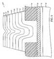
- the stack of layers formed between the first and second electrodesmay include alternating layers of chalcogenide glass 17 , 117 , 217 , 317 and metal containing layers 18 , 118 , 218 .
- a desirable metal containing layeris silver-selenide.
- a first chalcogenide glass layer 17is positioned over a first electrode 14
- a first silver-selenide layer 18is positioned over the first chalcogenide glass layer 17
- a second chalcogenide glass layer 117is positioned over the first silver-selenide layer 18
- a second silver-selenide layer 118is positioned over the second chalcogenide glass layer 117
- a third chalcogenide glass layer 217is positioned over the second silver-selenide layer 118
- a third silver-selenide layer 218is positioned over the third chalcogenide glass layer 217
- a fourth chalcogenide glass layer 317is positioned over the third silver-selenide layer 218 .
- the second conductive electrode 22can be formed over the fourth chalcogenide glass layer 317 .
- the memory element 100comprises at least two metal containing layers 18 , 118 and at least three chalcogenide glass layers 17 , 117 , 217 .
- the memory element 100may comprise a plurality of alternating layers of chalcogenide glass 17 , 117 , 217 and silver-selenide 18 , 118 , so long as the alternating layers start with a first chalcogenide glass layer, e.g 17 , and end with a last chalcogenide glass layer, e.g. 317 , with the first chalcogenide glass layer contacting a first electrode 14 and the last chalcogenide glass layer contacting a second electrode 22 .
- the thickness and ratios of the alternating layers of silver-selenide 18 , 118 , 218 and chalcogenide glass 17 , 117 , 217 , 317are the same as described above, in that the silver-selenide layers 18 , 118 , 218 are preferably thicker than connecting chalcogenide glass layers 17 , 117 , 217 , 317 in a ratio of between about 5:1 and about 1:1 silver-selenide layer 18 , 118 , 218 to connected chalcogenide glass layer 17 , 117 , 217 , 317 , and more preferably between about 3.3:1 and 2:1 silver-selenide layer 18 , 118 , 218 to connected chalcogenide glass layer 17 , 117 , 217 , 317 .
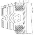
- one or more layers of a metal containing material 18 , 418may be deposited between the chalcogenide glass layers 17 , 117 .
- a plurality of silver-selenide layers 18 , 418may be used.
- an additional silver-selenide layer 418may be deposited on the first silver-selenide layer 18 and an additional silver-selenide layer 518 may be deposited on the third silver-selenide layer 218 .
- each of the chalcogenide glass layers 17 , 117 , 217 , 317 shown in FIG. 10may comprise a plurality of thinner layers of a chalcogenide glass material, such as germanium-selenide. Any suitable number of layers may be used to comprise the chalcogenide glass layers 17 , 117 , 217 , 317 .
- one or more of the chalcogenide glass layers 17 , 117 , 217 , 317may also be doped with a dopant such as a metal, which is preferably silver.
- a dopantsuch as a metal, which is preferably silver.
- Devices constructed according to the embodiments of the inventionparticularly those having a silver-selenide layer (e.g. layer 18 ) disposed between two chalcogenide glass layers (e.g. layers 17 , 20 ) show improved memory retention and write/erase performance over conventional memory devices. These devices have also shown data retention for more than 1200 hours at room temperature. The devices switch at pulse widths less than 2 nanoseconds compared with doped resistance variable memory elements of the prior art that switch at about 100 nanosecond pulses.
- a silver layer 50is provided above the second chalcogenide glass layer 20 .
- a conductive adhesion layer 30is then provided over the silver layer 50 and a top electrode 22 is provided over the conductive adhesion layer 30 .
- the silver layer 50may be deposited over the second glass layer 20 by any suitable means, such as sputtering or plating techniques, including electroplating or electroless plating.
- the desired thickness of the silver layeris about 200 ⁇ .
- Suitable materials for the conductive adhesion layerinclude conductive materials capable of providing good adhesion between the silver layer 50 and the top electrode layer 22 .
- Desirable materials for the conductive adhesion layer 30include chalcogenide glasses.
- a top electrode 22is then formed over the conductive adhesion layer 30 .
- the chalcogenide glass layers 17 , 20 of this exemplary embodimentcan be germanium-selenide glass having a Ge x Se 100-x stoichiometry, where x ranges from 17 to 43.
- the preferred stoichiometriesare about Ge 20 Se 80 to about Ge 43 Se 57 , most preferably about Ge 40 Se 60 .
- the first and second chalcogenide glass layers 17 , 20preferably have a thickness from about 100 ⁇ to about 1000 ⁇ and more preferably about 150 ⁇ .
- the metal containing layer 18can be any suitable metal containing material.
- suitable metal containing layers 18include silver-chalcogenide layers such as silver-selenide, silver-sulfide, silver-oxide, and silver-telluride among others.
- a desirable metal containing layeris silver-selenide.
- a variety of processescan be used to form the silver-selenide metal containing layer 18 . For instance, physical vapor deposition techniques such as evaporative deposition and sputtering may be used. Other processes such as chemical vapor deposition, co-evaporation or depositing a layer of selenium above a layer of silver to form silver-selenide can also be used.
- the metal containing layer 18can be about 1 to 5 times greater than the thickness of the first and second chalcogenide glass layers 17 , 20 and is preferably about 470 ⁇ .
- the top and bottom electrodes, 22 , 14can be any conductive material, such as tungsten, tantalum, aluminum, platinum, silver, conductive nitrides, and others.
- the bottom electrode 14is preferably tungsten.
- the top electrode 22is preferably tungsten or tantalum nitride.
- the conductive adhesion layer 30may be the same chalcogenide glass material used in the first and second chalcogenide glass layers 17 , 20 discussed above.
- the conductive adhesion layer 30can be formed by sputtering the chalcogenide glass onto the silver layer 50 .
- the energetic nature of the sputtering processmay cause a small amount of silver from the silver layer 50 to be incorporated into the chalcogenide glass adhesion layer 30 .
- the top electrodeshorts to the chalcogenide glass adhesion layer 30 , creating a conductive path from the top electrode to the first glass layer 17 .
- the desired thickness of a chalcogenide glass conductive adhesion layer 30is about 100 ⁇ .
- a conductive adhesion layer 30 between the silver layer 50 and the top electrode 22can prevent peeling of the top electrode 22 material during subsequent processing steps such as photoresist stripping. Electrode 22 materials, including tungsten, tantalum, tantalum-nitride, and titanium, among others, may not adhere well to silver layers 50 such as that shown in FIG. 11 . For example, adhesion between the two layers 50 , 22 may be insufficient to prevent the electrode 22 layer from at least partially separating (peeling) away from the underlying silver layer 50 and thus loosing electrical contact with the underlying layers 20 , 18 , 17 , 14 of the memory element 100 . Poor contact between the top electrode 22 and the underlying memory element layers 20 , 18 , 17 , 14 can lead to electrical performance problems and unreliable switching characteristics. Use of a conductive binding layer 30 can substantially eliminate this problem.
- the silver selenide layer 18provides a source of silver selenide, which is driven into chalcogenide glass layer 17 by a conditioning step after formation of the memory element 100 ( FIG. 11 ).
- the conditioning stepcomprises applying a potential across the memory element structure 100 such that silver selenide from the silver selenide layer 18 is driven into the first chalcogenide glass layers 17 , forming a conducting channel.
- the pulse width and amplitudeare critical parameters of the conditioning potential, which generally has a longer pulse width and higher amplitude than a typical potential used to program the memory element.
- the memory element 100may be programmed, provide that some silver moved into the conductive channel during conditioning.
- agglomeration of silver at the silver layer 50 /silver-selenide layer 18 interfacemay occur during deposition. Such silver agglomeration can cause subsequent processing problems during operation of the memory cell 100 .
- Use of a chalcogenide glass layer 20 between the silver layer 50 and the silver-selenide layer 18can prevent silver agglomeration on the surface of the silver-selenide layer 18 .
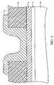
- an additional silver layer 40can be deposited between the lower chalcogenide glass layer 17 and the silver selenide glass layer 18 , as shown in FIG. 12 .
- a memory element 200as illustrated in FIG. 12 , comprises a first chalcogenide glass layer 17 , a first silver layer 40 , a silver-selenide glass layer 18 , a second chalcogenide glass layer 20 , a second silver layer 50 ′, a conductive adhesion layer 30 , and a top electrode layer 22 . Addition of the first silver layer 40 minimizes the amplitude and pulse width of the conditioning potential needed prior to write and erase operations.
- first chalcogenide glass layer 17may be a doped chalcogenide glass.
- the first chalcogenide glass layermay be silver-doped silver selenide.
- a conditioning stepallows silver selenide from the silver selenide layer 18 to be incorporated into the first chalcogenide glass layer 17 .
- Deposition of the silver selenide layer 18 over the silver layer 40causes the silver selenide layer 18 to become silver-rich.
- This silver-rich silver selenidemore easily incorporates into the first chalcogenide glass layer 17 under the influence of an applied conditioning pulse.
- the conditioning pulsecan have a shorter pulse width and lower amplitude, effectively speeding up the conditioning process.
- the first silver layer 40must be relatively thin in comparison to the second silver layer 50 ′, in order to prevent an excess of silver from being incorporated into the lower chalcogenide layer during conditioning, which can shorten the life of the memory element.
- the first silver layer 40has a desired thickness of about 35-50 ⁇ when the first glass layer 17 is about 150 ⁇
- a silver layer 40 ′is provided above a chalcogenide glass layer 17 .
- a memory element 300as illustrated in FIG. 13 , comprises a first chalcogenide glass layer 17 , a silver layer 40 ′, a silver-selenide glass layer 18 , a second chalcogenide glass layer 20 , and a top electrode layer 22 .
- a conditioning stepdrives silver selenide from the silver selenide layer 18 into the first chalcogenide glass layer 17 , opening a conductive channel.
- a silver layer 50 ′is provided above the second glass layer 20 .
- the silver layer 50 ′may be deposited over the second glass layer 20 by any suitable means, such as sputtering or plating techniques, including electroplating or electroless plating.
- the desired thickness of the silver layeris about 200 ⁇ .
- a top electrode 22is then formed over the silver layer 50 ′.
- a memory element 400as illustrated in FIG.
- the first chalcogenide glass layer 17may be a doped chalcogenide glass.
- the first chalcogenide glass layermay be silver-doped silver selenide.
- FIG. 15illustrates a typical processor system 400 which includes a memory circuit 448 , for example a programmable conductor RAM, which employs resistance variable memory elements fabricated in accordance with the invention.
- a processor systemsuch as a computer system, generally comprises a central processing unit (CPU) 444 , such as a microprocessor, a digital signal processor, or other programmable digital logic devices, which communicates with an input/output (I/O) device 446 over a bus 452 .
- the memory 448communicates with the system over bus 452 typically through a memory controller.
- the processor systemmay include peripheral devices such as a floppy disk drive 454 and a compact disc (CD) ROM drive 456 , which also communicate with CPU 444 over the bus 452 .
- Memory 448is preferably constructed as an integrated circuit, which includes one or more resistance variable memory elements 100 . If desired, the memory 448 may be combined with the processor, for example CPU 444 , in a single integrated circuit.
Landscapes
- Engineering & Computer Science (AREA)
- Manufacturing & Machinery (AREA)
- Semiconductor Memories (AREA)
- Glass Compositions (AREA)
Abstract
Description
Claims (7)
Priority Applications (2)
| Application Number | Priority Date | Filing Date | Title |
|---|---|---|---|
| US11/443,266US7723713B2 (en) | 2002-02-20 | 2006-05-31 | Layered resistance variable memory device and method of fabrication |
| US12/771,224US8263958B2 (en) | 2002-02-20 | 2010-04-30 | Layered resistance variable memory device and method of fabrication |
Applications Claiming Priority (4)
| Application Number | Priority Date | Filing Date | Title |
|---|---|---|---|
| US7786702A | 2002-02-20 | 2002-02-20 | |
| US10/120,521US7151273B2 (en) | 2002-02-20 | 2002-04-12 | Silver-selenide/chalcogenide glass stack for resistance variable memory |
| US10/819,315US7087919B2 (en) | 2002-02-20 | 2004-04-07 | Layered resistance variable memory device and method of fabrication |
| US11/443,266US7723713B2 (en) | 2002-02-20 | 2006-05-31 | Layered resistance variable memory device and method of fabrication |
Related Parent Applications (2)
| Application Number | Title | Priority Date | Filing Date |
|---|---|---|---|
| US10/819,315ContinuationUS7087919B2 (en) | 2002-02-20 | 2004-04-07 | Layered resistance variable memory device and method of fabrication |
| US12/771,224ContinuationUS8263958B2 (en) | 2002-02-20 | 2010-04-30 | Layered resistance variable memory device and method of fabrication |
Related Child Applications (1)
| Application Number | Title | Priority Date | Filing Date |
|---|---|---|---|
| US12/771,224DivisionUS8263958B2 (en) | 2002-02-20 | 2010-04-30 | Layered resistance variable memory device and method of fabrication |
Publications (2)
| Publication Number | Publication Date |
|---|---|
| US20070007506A1 US20070007506A1 (en) | 2007-01-11 |
| US7723713B2true US7723713B2 (en) | 2010-05-25 |
Family
ID=27759920
Family Applications (6)
| Application Number | Title | Priority Date | Filing Date |
|---|---|---|---|
| US10/120,521Expired - Fee RelatedUS7151273B2 (en) | 2002-02-20 | 2002-04-12 | Silver-selenide/chalcogenide glass stack for resistance variable memory |
| US11/443,266Expired - LifetimeUS7723713B2 (en) | 2002-02-20 | 2006-05-31 | Layered resistance variable memory device and method of fabrication |
| US11/585,259Expired - LifetimeUS7646007B2 (en) | 2002-02-20 | 2006-10-24 | Silver-selenide/chalcogenide glass stack for resistance variable memory |
| US12/630,700Expired - Fee RelatedUS8080816B2 (en) | 2002-02-20 | 2009-12-03 | Silver-selenide/chalcogenide glass stack for resistance variable memory |
| US12/771,224Expired - Fee RelatedUS8263958B2 (en) | 2002-02-20 | 2010-04-30 | Layered resistance variable memory device and method of fabrication |
| US13/303,276Expired - Fee RelatedUS8466445B2 (en) | 2002-02-20 | 2011-11-23 | Silver-selenide/chalcogenide glass stack for resistance variable memory and manufacturing method thereof |
Family Applications Before (1)
| Application Number | Title | Priority Date | Filing Date |
|---|---|---|---|
| US10/120,521Expired - Fee RelatedUS7151273B2 (en) | 2002-02-20 | 2002-04-12 | Silver-selenide/chalcogenide glass stack for resistance variable memory |
Family Applications After (4)
| Application Number | Title | Priority Date | Filing Date |
|---|---|---|---|
| US11/585,259Expired - LifetimeUS7646007B2 (en) | 2002-02-20 | 2006-10-24 | Silver-selenide/chalcogenide glass stack for resistance variable memory |
| US12/630,700Expired - Fee RelatedUS8080816B2 (en) | 2002-02-20 | 2009-12-03 | Silver-selenide/chalcogenide glass stack for resistance variable memory |
| US12/771,224Expired - Fee RelatedUS8263958B2 (en) | 2002-02-20 | 2010-04-30 | Layered resistance variable memory device and method of fabrication |
| US13/303,276Expired - Fee RelatedUS8466445B2 (en) | 2002-02-20 | 2011-11-23 | Silver-selenide/chalcogenide glass stack for resistance variable memory and manufacturing method thereof |
Country Status (8)
| Country | Link |
|---|---|
| US (6) | US7151273B2 (en) |
| EP (1) | EP1476909A2 (en) |
| JP (1) | JP2005518665A (en) |
| KR (1) | KR100641973B1 (en) |
| CN (1) | CN100483767C (en) |
| AU (1) | AU2003217405A1 (en) |
| TW (1) | TW586117B (en) |
| WO (1) | WO2003071614A2 (en) |
Cited By (9)
| Publication number | Priority date | Publication date | Assignee | Title |
|---|---|---|---|---|
| US20080248380A1 (en)* | 2007-04-05 | 2008-10-09 | Philippe Blanchard | Method of manufacturing an integrated circuit, an integrated circuit, and a memory module |
| US20110076826A1 (en)* | 2009-09-25 | 2011-03-31 | Applied Materials, Inc. | Passivating glue layer to improve amorphous carbon to metal adhesion |
| US7924608B2 (en) | 2006-10-19 | 2011-04-12 | Boise State University | Forced ion migration for chalcogenide phase change memory device |
| US8238146B2 (en) | 2008-08-01 | 2012-08-07 | Boise State University | Variable integrated analog resistor |
| US8284590B2 (en) | 2010-05-06 | 2012-10-09 | Boise State University | Integratable programmable capacitive device |
| US8467236B2 (en) | 2008-08-01 | 2013-06-18 | Boise State University | Continuously variable resistor |
| US9281474B2 (en) | 2011-08-09 | 2016-03-08 | Kabushiki Kaisha Toshiba | Variable resistance memory and method of manufacturing the same |
| US9583703B2 (en) | 2015-06-01 | 2017-02-28 | Boise State University | Tunable variable resistance memory device |
| US9583699B2 (en) | 2015-06-01 | 2017-02-28 | Boise State University | Tunable variable resistance memory device |
Families Citing this family (166)
| Publication number | Priority date | Publication date | Assignee | Title |
|---|---|---|---|---|
| US6734455B2 (en) | 2001-03-15 | 2004-05-11 | Micron Technology, Inc. | Agglomeration elimination for metal sputter deposition of chalcogenides |
| US7102150B2 (en) | 2001-05-11 | 2006-09-05 | Harshfield Steven T | PCRAM memory cell and method of making same |
| US6951805B2 (en)* | 2001-08-01 | 2005-10-04 | Micron Technology, Inc. | Method of forming integrated circuitry, method of forming memory circuitry, and method of forming random access memory circuitry |
| US6881623B2 (en) | 2001-08-29 | 2005-04-19 | Micron Technology, Inc. | Method of forming chalcogenide comprising devices, method of forming a programmable memory cell of memory circuitry, and a chalcogenide comprising device |
| US6784018B2 (en) | 2001-08-29 | 2004-08-31 | Micron Technology, Inc. | Method of forming chalcogenide comprising devices and method of forming a programmable memory cell of memory circuitry |
| US6955940B2 (en) | 2001-08-29 | 2005-10-18 | Micron Technology, Inc. | Method of forming chalcogenide comprising devices |
| US6646902B2 (en) | 2001-08-30 | 2003-11-11 | Micron Technology, Inc. | Method of retaining memory state in a programmable conductor RAM |
| US6815818B2 (en) | 2001-11-19 | 2004-11-09 | Micron Technology, Inc. | Electrode structure for use in an integrated circuit |
| US6791859B2 (en) | 2001-11-20 | 2004-09-14 | Micron Technology, Inc. | Complementary bit PCRAM sense amplifier and method of operation |
| US6867064B2 (en)* | 2002-02-15 | 2005-03-15 | Micron Technology, Inc. | Method to alter chalcogenide glass for improved switching characteristics |
| US6791885B2 (en) | 2002-02-19 | 2004-09-14 | Micron Technology, Inc. | Programmable conductor random access memory and method for sensing same |
| US6809362B2 (en) | 2002-02-20 | 2004-10-26 | Micron Technology, Inc. | Multiple data state memory cell |
| US7151273B2 (en) | 2002-02-20 | 2006-12-19 | Micron Technology, Inc. | Silver-selenide/chalcogenide glass stack for resistance variable memory |
| US7087919B2 (en)* | 2002-02-20 | 2006-08-08 | Micron Technology, Inc. | Layered resistance variable memory device and method of fabrication |
| US6891749B2 (en)* | 2002-02-20 | 2005-05-10 | Micron Technology, Inc. | Resistance variable ‘on ’ memory |
| US6849868B2 (en) | 2002-03-14 | 2005-02-01 | Micron Technology, Inc. | Methods and apparatus for resistance variable material cells |
| US6855975B2 (en) | 2002-04-10 | 2005-02-15 | Micron Technology, Inc. | Thin film diode integrated with chalcogenide memory cell |
| US6858482B2 (en) | 2002-04-10 | 2005-02-22 | Micron Technology, Inc. | Method of manufacture of programmable switching circuits and memory cells employing a glass layer |
| US6864500B2 (en)* | 2002-04-10 | 2005-03-08 | Micron Technology, Inc. | Programmable conductor memory cell structure |
| US6890790B2 (en) | 2002-06-06 | 2005-05-10 | Micron Technology, Inc. | Co-sputter deposition of metal-doped chalcogenides |
| US7015494B2 (en)* | 2002-07-10 | 2006-03-21 | Micron Technology, Inc. | Assemblies displaying differential negative resistance |
| US6872963B2 (en)* | 2002-08-08 | 2005-03-29 | Ovonyx, Inc. | Programmable resistance memory element with layered memory material |
| US7209378B2 (en) | 2002-08-08 | 2007-04-24 | Micron Technology, Inc. | Columnar 1T-N memory cell structure |
| US7018863B2 (en) | 2002-08-22 | 2006-03-28 | Micron Technology, Inc. | Method of manufacture of a resistance variable memory cell |
| US6831019B1 (en) | 2002-08-29 | 2004-12-14 | Micron Technology, Inc. | Plasma etching methods and methods of forming memory devices comprising a chalcogenide comprising layer received operably proximate conductive electrodes |
| US6867996B2 (en)* | 2002-08-29 | 2005-03-15 | Micron Technology, Inc. | Single-polarity programmable resistance-variable memory element |
| US6867114B2 (en) | 2002-08-29 | 2005-03-15 | Micron Technology Inc. | Methods to form a memory cell with metal-rich metal chalcogenide |
| US7163837B2 (en)* | 2002-08-29 | 2007-01-16 | Micron Technology, Inc. | Method of forming a resistance variable memory element |
| US7294527B2 (en) | 2002-08-29 | 2007-11-13 | Micron Technology Inc. | Method of forming a memory cell |
| US7364644B2 (en) | 2002-08-29 | 2008-04-29 | Micron Technology, Inc. | Silver selenide film stoichiometry and morphology control in sputter deposition |
| US6864521B2 (en) | 2002-08-29 | 2005-03-08 | Micron Technology, Inc. | Method to control silver concentration in a resistance variable memory element |
| US7022579B2 (en) | 2003-03-14 | 2006-04-04 | Micron Technology, Inc. | Method for filling via with metal |
| US6930909B2 (en) | 2003-06-25 | 2005-08-16 | Micron Technology, Inc. | Memory device and methods of controlling resistance variation and resistance profile drift |
| US6961277B2 (en) | 2003-07-08 | 2005-11-01 | Micron Technology, Inc. | Method of refreshing a PCRAM memory device |
| US7061004B2 (en) | 2003-07-21 | 2006-06-13 | Micron Technology, Inc. | Resistance variable memory elements and methods of formation |
| US6903361B2 (en) | 2003-09-17 | 2005-06-07 | Micron Technology, Inc. | Non-volatile memory structure |
| US7015504B2 (en)* | 2003-11-03 | 2006-03-21 | Advanced Micro Devices, Inc. | Sidewall formation for high density polymer memory element array |
| WO2005081256A1 (en)* | 2004-02-19 | 2005-09-01 | Agency For Science, Technology And Research | Electrically writeable and erasable memory medium |
| US7098068B2 (en) | 2004-03-10 | 2006-08-29 | Micron Technology, Inc. | Method of forming a chalcogenide material containing device |
| US7583551B2 (en) | 2004-03-10 | 2009-09-01 | Micron Technology, Inc. | Power management control and controlling memory refresh operations |
| DE102004025083A1 (en)* | 2004-05-21 | 2005-12-29 | Infineon Technologies Ag | Production of a solid body electrolyte material region made from a chalcogenide material comprises using germanium and/or silicon as precursor compound or carrier compound in the form of an organic compound |
| DE102004029436B4 (en)* | 2004-06-18 | 2009-03-05 | Qimonda Ag | A method of manufacturing a solid electrolyte material region |
| US7326950B2 (en) | 2004-07-19 | 2008-02-05 | Micron Technology, Inc. | Memory device with switching glass layer |
| US7354793B2 (en) | 2004-08-12 | 2008-04-08 | Micron Technology, Inc. | Method of forming a PCRAM device incorporating a resistance-variable chalocogenide element |
| US7190048B2 (en) | 2004-07-19 | 2007-03-13 | Micron Technology, Inc. | Resistance variable memory device and method of fabrication |
| JP4830275B2 (en)* | 2004-07-22 | 2011-12-07 | ソニー株式会社 | Memory element |
| US7365411B2 (en) | 2004-08-12 | 2008-04-29 | Micron Technology, Inc. | Resistance variable memory with temperature tolerant materials |
| US20060045974A1 (en)* | 2004-08-25 | 2006-03-02 | Campbell Kristy A | Wet chemical method to form silver-rich silver-selenide |
| US7151688B2 (en) | 2004-09-01 | 2006-12-19 | Micron Technology, Inc. | Sensing of resistance variable memory devices |
| DE102004046804B4 (en)* | 2004-09-27 | 2006-10-05 | Infineon Technologies Ag | Resistively switching semiconductor memory |
| US7023008B1 (en)* | 2004-09-30 | 2006-04-04 | Infineon Technologies Ag | Resistive memory element |
| JP2006120707A (en)* | 2004-10-19 | 2006-05-11 | Matsushita Electric Ind Co Ltd | Variable resistance element and semiconductor device |
| DE102004052647B4 (en) | 2004-10-29 | 2009-01-02 | Qimonda Ag | Method for improving the thermal properties of semiconductor memory cells in the manufacturing process and non-volatile, resistively switching memory cell |
| DE102004052645A1 (en)* | 2004-10-29 | 2006-05-04 | Infineon Technologies Ag | Non-volatile (sic) resistive storage cell with solid electrolyte matrix between first and second electrode as active layer useful in semiconductor technology has elements from groups IVb and Vb and transition metals in active layer |
| US7326951B2 (en)* | 2004-12-16 | 2008-02-05 | Macronix International Co., Ltd. | Chalcogenide random access memory |
| US7374174B2 (en) | 2004-12-22 | 2008-05-20 | Micron Technology, Inc. | Small electrode for resistance variable devices |
| US20060131555A1 (en)* | 2004-12-22 | 2006-06-22 | Micron Technology, Inc. | Resistance variable devices with controllable channels |
| JP2006210718A (en)* | 2005-01-28 | 2006-08-10 | Renesas Technology Corp | Semiconductor device manufacturing method and semiconductor device |
| US7317200B2 (en) | 2005-02-23 | 2008-01-08 | Micron Technology, Inc. | SnSe-based limited reprogrammable cell |
| US8653495B2 (en)* | 2005-04-11 | 2014-02-18 | Micron Technology, Inc. | Heating phase change material |
| US7269044B2 (en) | 2005-04-22 | 2007-09-11 | Micron Technology, Inc. | Method and apparatus for accessing a memory array |
| US7427770B2 (en) | 2005-04-22 | 2008-09-23 | Micron Technology, Inc. | Memory array for increased bit density |
| US7709289B2 (en) | 2005-04-22 | 2010-05-04 | Micron Technology, Inc. | Memory elements having patterned electrodes and method of forming the same |
| US7269079B2 (en) | 2005-05-16 | 2007-09-11 | Micron Technology, Inc. | Power circuits for reducing a number of power supply voltage taps required for sensing a resistive memory |
| JP4862113B2 (en)* | 2005-05-19 | 2012-01-25 | エヌエックスピー ビー ヴィ | Method for controlling a "premelted" region in a PCM cell and device obtained therefrom |
| US7233520B2 (en) | 2005-07-08 | 2007-06-19 | Micron Technology, Inc. | Process for erasing chalcogenide variable resistance memory bits |
| US7655938B2 (en)* | 2005-07-20 | 2010-02-02 | Kuo Charles C | Phase change memory with U-shaped chalcogenide cell |
| US7274034B2 (en) | 2005-08-01 | 2007-09-25 | Micron Technology, Inc. | Resistance variable memory device with sputtered metal-chalcogenide region and method of fabrication |
| US7332735B2 (en) | 2005-08-02 | 2008-02-19 | Micron Technology, Inc. | Phase change memory cell and method of formation |
| US7317567B2 (en) | 2005-08-02 | 2008-01-08 | Micron Technology, Inc. | Method and apparatus for providing color changing thin film material |
| US7579615B2 (en) | 2005-08-09 | 2009-08-25 | Micron Technology, Inc. | Access transistor for memory device |
| US7304368B2 (en) | 2005-08-11 | 2007-12-04 | Micron Technology, Inc. | Chalcogenide-based electrokinetic memory element and method of forming the same |
| US7521705B2 (en)* | 2005-08-15 | 2009-04-21 | Micron Technology, Inc. | Reproducible resistance variable insulating memory devices having a shaped bottom electrode |
| US7251154B2 (en) | 2005-08-15 | 2007-07-31 | Micron Technology, Inc. | Method and apparatus providing a cross-point memory array using a variable resistance memory cell and capacitance |
| US20070045606A1 (en)* | 2005-08-30 | 2007-03-01 | Michele Magistretti | Shaping a phase change layer in a phase change memory cell |
| US7277313B2 (en) | 2005-08-31 | 2007-10-02 | Micron Technology, Inc. | Resistance variable memory element with threshold device and method of forming the same |
| KR20080072697A (en)* | 2005-11-01 | 2008-08-06 | 사이더로믹스, 엘엘씨 | Growth Control of Oral and Surface Microorganisms Using Gallium Compounds |
| US7786460B2 (en) | 2005-11-15 | 2010-08-31 | Macronix International Co., Ltd. | Phase change memory device and manufacturing method |
| US7635855B2 (en) | 2005-11-15 | 2009-12-22 | Macronix International Co., Ltd. | I-shaped phase change memory cell |
| US7449710B2 (en) | 2005-11-21 | 2008-11-11 | Macronix International Co., Ltd. | Vacuum jacket for phase change memory element |
| US7688619B2 (en) | 2005-11-28 | 2010-03-30 | Macronix International Co., Ltd. | Phase change memory cell and manufacturing method |
| US7943921B2 (en) | 2005-12-16 | 2011-05-17 | Micron Technology, Inc. | Phase change current density control structure |
| JP2007180174A (en)* | 2005-12-27 | 2007-07-12 | Fujitsu Ltd | Resistance change memory element |
| US7910907B2 (en)* | 2006-03-15 | 2011-03-22 | Macronix International Co., Ltd. | Manufacturing method for pipe-shaped electrode phase change memory |
| WO2007116749A1 (en)* | 2006-03-30 | 2007-10-18 | Matsushita Electric Industrial Co., Ltd. | Nonvolatile memory element and its manufacturing method |
| US7626190B2 (en)* | 2006-06-02 | 2009-12-01 | Infineon Technologies Ag | Memory device, in particular phase change random access memory device with transistor, and method for fabricating a memory device |
| US7785920B2 (en) | 2006-07-12 | 2010-08-31 | Macronix International Co., Ltd. | Method for making a pillar-type phase change memory element |
| KR100798696B1 (en)* | 2006-08-18 | 2008-01-28 | 충남대학교산학협력단 | PMCM element having a solid electrolyte composed of silver-saturated thin-film thin film and method for manufacturing same |
| US7964869B2 (en)* | 2006-08-25 | 2011-06-21 | Panasonic Corporation | Memory element, memory apparatus, and semiconductor integrated circuit |
| US7560723B2 (en) | 2006-08-29 | 2009-07-14 | Micron Technology, Inc. | Enhanced memory density resistance variable memory cells, arrays, devices and systems including the same, and methods of fabrication |
| US7772581B2 (en)* | 2006-09-11 | 2010-08-10 | Macronix International Co., Ltd. | Memory device having wide area phase change element and small electrode contact area |
| US7504653B2 (en) | 2006-10-04 | 2009-03-17 | Macronix International Co., Ltd. | Memory cell device with circumferentially-extending memory element |
| US8796660B2 (en)* | 2006-10-16 | 2014-08-05 | Panasonic Corporation | Nonvolatile memory element comprising a resistance variable element and a diode |
| US7476587B2 (en) | 2006-12-06 | 2009-01-13 | Macronix International Co., Ltd. | Method for making a self-converged memory material element for memory cell |
| US7903447B2 (en) | 2006-12-13 | 2011-03-08 | Macronix International Co., Ltd. | Method, apparatus and computer program product for read before programming process on programmable resistive memory cell |
| US7718989B2 (en) | 2006-12-28 | 2010-05-18 | Macronix International Co., Ltd. | Resistor random access memory cell device |
| US7786461B2 (en) | 2007-04-03 | 2010-08-31 | Macronix International Co., Ltd. | Memory structure with reduced-size memory element between memory material portions |
| KR100852206B1 (en)* | 2007-04-04 | 2008-08-13 | 삼성전자주식회사 | Resistive memory device and manufacturing method thereof. |
| KR101350979B1 (en)* | 2007-05-11 | 2014-01-14 | 삼성전자주식회사 | Resistive memory device and Manufacturing Method for the same |
| KR100891523B1 (en) | 2007-07-20 | 2009-04-06 | 주식회사 하이닉스반도체 | Phase change memory device |
| US7729161B2 (en) | 2007-08-02 | 2010-06-01 | Macronix International Co., Ltd. | Phase change memory with dual word lines and source lines and method of operating same |
| WO2009051799A1 (en)* | 2007-10-18 | 2009-04-23 | Structured Materials Inc. | Germanium sulfide compounds for solid electrolytic memory elements |
| US7919766B2 (en) | 2007-10-22 | 2011-04-05 | Macronix International Co., Ltd. | Method for making self aligning pillar memory cell device |
| JP4427630B2 (en)* | 2007-11-15 | 2010-03-10 | パナソニック株式会社 | Nonvolatile memory device and manufacturing method thereof |
| US7961507B2 (en) | 2008-03-11 | 2011-06-14 | Micron Technology, Inc. | Non-volatile memory with resistive access component |
| US7579210B1 (en)* | 2008-03-25 | 2009-08-25 | Ovonyx, Inc. | Planar segmented contact |
| US8077505B2 (en) | 2008-05-07 | 2011-12-13 | Macronix International Co., Ltd. | Bipolar switching of phase change device |
| KR101141008B1 (en)* | 2008-06-18 | 2012-05-02 | 캐논 아네르바 가부시키가이샤 | Phase-change memory element, phase-change memory cell, vacuum treatment device, and method for manufacturing phase-change memory element |
| US8742387B2 (en)* | 2008-06-25 | 2014-06-03 | Qimonda Ag | Resistive memory devices with improved resistive changing elements |
| US8134857B2 (en) | 2008-06-27 | 2012-03-13 | Macronix International Co., Ltd. | Methods for high speed reading operation of phase change memory and device employing same |
| US7932506B2 (en) | 2008-07-22 | 2011-04-26 | Macronix International Co., Ltd. | Fully self-aligned pore-type memory cell having diode access device |
| US7825479B2 (en)* | 2008-08-06 | 2010-11-02 | International Business Machines Corporation | Electrical antifuse having a multi-thickness dielectric layer |
| US7903457B2 (en) | 2008-08-19 | 2011-03-08 | Macronix International Co., Ltd. | Multiple phase change materials in an integrated circuit for system on a chip application |
| US7719913B2 (en) | 2008-09-12 | 2010-05-18 | Macronix International Co., Ltd. | Sensing circuit for PCRAM applications |
| US8324605B2 (en) | 2008-10-02 | 2012-12-04 | Macronix International Co., Ltd. | Dielectric mesh isolated phase change structure for phase change memory |
| US8036014B2 (en) | 2008-11-06 | 2011-10-11 | Macronix International Co., Ltd. | Phase change memory program method without over-reset |
| US7869270B2 (en) | 2008-12-29 | 2011-01-11 | Macronix International Co., Ltd. | Set algorithm for phase change memory cell |
| US8089137B2 (en) | 2009-01-07 | 2012-01-03 | Macronix International Co., Ltd. | Integrated circuit memory with single crystal silicon on silicide driver and manufacturing method |
| US8107283B2 (en) | 2009-01-12 | 2012-01-31 | Macronix International Co., Ltd. | Method for setting PCRAM devices |
| US8030635B2 (en) | 2009-01-13 | 2011-10-04 | Macronix International Co., Ltd. | Polysilicon plug bipolar transistor for phase change memory |
| US8064247B2 (en) | 2009-01-14 | 2011-11-22 | Macronix International Co., Ltd. | Rewritable memory device based on segregation/re-absorption |
| US8933536B2 (en) | 2009-01-22 | 2015-01-13 | Macronix International Co., Ltd. | Polysilicon pillar bipolar transistor with self-aligned memory element |
| US8134138B2 (en) | 2009-01-30 | 2012-03-13 | Seagate Technology Llc | Programmable metallization memory cell with planarized silver electrode |
| US8084760B2 (en) | 2009-04-20 | 2011-12-27 | Macronix International Co., Ltd. | Ring-shaped electrode and manufacturing method for same |
| US8426839B1 (en)* | 2009-04-24 | 2013-04-23 | Adesto Technologies Corporation | Conducting bridge random access memory (CBRAM) device structures |
| US8173987B2 (en) | 2009-04-27 | 2012-05-08 | Macronix International Co., Ltd. | Integrated circuit 3D phase change memory array and manufacturing method |
| US8097871B2 (en) | 2009-04-30 | 2012-01-17 | Macronix International Co., Ltd. | Low operational current phase change memory structures |
| US7933139B2 (en) | 2009-05-15 | 2011-04-26 | Macronix International Co., Ltd. | One-transistor, one-resistor, one-capacitor phase change memory |
| US8350316B2 (en) | 2009-05-22 | 2013-01-08 | Macronix International Co., Ltd. | Phase change memory cells having vertical channel access transistor and memory plane |
| US7968876B2 (en) | 2009-05-22 | 2011-06-28 | Macronix International Co., Ltd. | Phase change memory cell having vertical channel access transistor |
| US8809829B2 (en) | 2009-06-15 | 2014-08-19 | Macronix International Co., Ltd. | Phase change memory having stabilized microstructure and manufacturing method |
| US8406033B2 (en) | 2009-06-22 | 2013-03-26 | Macronix International Co., Ltd. | Memory device and method for sensing and fixing margin cells |
| US8363463B2 (en) | 2009-06-25 | 2013-01-29 | Macronix International Co., Ltd. | Phase change memory having one or more non-constant doping profiles |
| US8238149B2 (en) | 2009-06-25 | 2012-08-07 | Macronix International Co., Ltd. | Methods and apparatus for reducing defect bits in phase change memory |
| US8110822B2 (en) | 2009-07-15 | 2012-02-07 | Macronix International Co., Ltd. | Thermal protect PCRAM structure and methods for making |
| US7894254B2 (en) | 2009-07-15 | 2011-02-22 | Macronix International Co., Ltd. | Refresh circuitry for phase change memory |
| US8198619B2 (en) | 2009-07-15 | 2012-06-12 | Macronix International Co., Ltd. | Phase change memory cell structure |
| US8064248B2 (en) | 2009-09-17 | 2011-11-22 | Macronix International Co., Ltd. | 2T2R-1T1R mix mode phase change memory array |
| US20110079709A1 (en)* | 2009-10-07 | 2011-04-07 | Campbell Kristy A | Wide band sensor |
| US8178387B2 (en) | 2009-10-23 | 2012-05-15 | Macronix International Co., Ltd. | Methods for reducing recrystallization time for a phase change material |
| US20110192320A1 (en)* | 2010-02-09 | 2011-08-11 | Silberline Manufacturing Company, Inc. | Black metallic effect pigments |
| US8729521B2 (en) | 2010-05-12 | 2014-05-20 | Macronix International Co., Ltd. | Self aligned fin-type programmable memory cell |
| US8310864B2 (en) | 2010-06-15 | 2012-11-13 | Macronix International Co., Ltd. | Self-aligned bit line under word line memory array |
| CN102576709B (en)* | 2010-08-17 | 2015-03-04 | 松下电器产业株式会社 | Non-volatile memory device and manufacturing method thereof |
| US8395935B2 (en) | 2010-10-06 | 2013-03-12 | Macronix International Co., Ltd. | Cross-point self-aligned reduced cell size phase change memory |
| JP5348108B2 (en)* | 2010-10-18 | 2013-11-20 | ソニー株式会社 | Memory element |
| US8497705B2 (en) | 2010-11-09 | 2013-07-30 | Macronix International Co., Ltd. | Phase change device for interconnection of programmable logic device |
| US8227785B2 (en)* | 2010-11-11 | 2012-07-24 | Micron Technology, Inc. | Chalcogenide containing semiconductors with chalcogenide gradient |
| US8467238B2 (en) | 2010-11-15 | 2013-06-18 | Macronix International Co., Ltd. | Dynamic pulse operation for phase change memory |
| US20120168233A1 (en)* | 2010-12-30 | 2012-07-05 | Purdue Research Foundation | Robotic devices and methods |
| US9054295B2 (en)* | 2011-08-23 | 2015-06-09 | Micron Technology, Inc. | Phase change memory cells including nitrogenated carbon materials, methods of forming the same, and phase change memory devices including nitrogenated carbon materials |
| KR20130142518A (en)* | 2012-06-19 | 2013-12-30 | 에스케이하이닉스 주식회사 | Resistive memory device, memory apparatus and data processing system having the same |
| US8729519B2 (en)* | 2012-10-23 | 2014-05-20 | Micron Technology, Inc. | Memory constructions |
| KR102077641B1 (en) | 2013-08-06 | 2020-02-14 | 삼성전자주식회사 | Phase-change material layer and method of manufacturing the same |
| US9559113B2 (en) | 2014-05-01 | 2017-01-31 | Macronix International Co., Ltd. | SSL/GSL gate oxide in 3D vertical channel NAND |
| US9425389B2 (en)* | 2014-12-08 | 2016-08-23 | Intermolecular, Inc. | Doped ternary nitride embedded resistors for resistive random access memory cells |
| SG11201705757XA (en)* | 2015-01-26 | 2017-08-30 | Agency Science Tech & Res | Memory cell selector and method of operating memory cell |
| US9379321B1 (en)* | 2015-03-20 | 2016-06-28 | Intel Corporation | Chalcogenide glass composition and chalcogenide switch devices |
| US9672906B2 (en) | 2015-06-19 | 2017-06-06 | Macronix International Co., Ltd. | Phase change memory with inter-granular switching |
| US11003981B2 (en) | 2017-05-25 | 2021-05-11 | International Business Machines Corporation | Two-terminal metastable mixed-conductor memristive devices |
| US10340447B2 (en) | 2017-06-07 | 2019-07-02 | International Business Machines Corporation | Three-terminal metastable symmetric zero-volt battery memristive device |
| CN107732010B (en)* | 2017-09-29 | 2020-07-10 | 华中科技大学 | Gate tube device and preparation method thereof |
| KR102549544B1 (en) | 2018-09-03 | 2023-06-29 | 삼성전자주식회사 | Memory devices |
| KR102030341B1 (en)* | 2018-12-19 | 2019-10-10 | 한양대학교 산학협력단 | Selective device and memory device including the same |
| US11271151B2 (en)* | 2019-06-12 | 2022-03-08 | International Business Machines Corporation | Phase change memory using multiple phase change layers and multiple heat conductors |
| CN111116201B (en)* | 2020-01-07 | 2021-01-15 | 北京科技大学 | A kind of preparation method of GeS-based thermoelectric material |
Citations (187)
| Publication number | Priority date | Publication date | Assignee | Title |
|---|---|---|---|---|
| US3271591A (en) | 1963-09-20 | 1966-09-06 | Energy Conversion Devices Inc | Symmetrical current controlling device |
| US3622319A (en) | 1966-10-20 | 1971-11-23 | Western Electric Co | Nonreflecting photomasks and methods of making same |
| US3743847A (en) | 1971-06-01 | 1973-07-03 | Motorola Inc | Amorphous silicon film as a uv filter |
| US3961314A (en) | 1974-03-05 | 1976-06-01 | Energy Conversion Devices, Inc. | Structure and method for producing an image |
| US3966317A (en) | 1974-04-08 | 1976-06-29 | Energy Conversion Devices, Inc. | Dry process production of archival microform records from hard copy |
| US3983542A (en) | 1970-08-13 | 1976-09-28 | Energy Conversion Devices, Inc. | Method and apparatus for recording information |
| US4177474A (en) | 1977-05-18 | 1979-12-04 | Energy Conversion Devices, Inc. | High temperature amorphous semiconductor member and method of making the same |
| US4267261A (en) | 1971-07-15 | 1981-05-12 | Energy Conversion Devices, Inc. | Method for full format imaging |
| US4269935A (en) | 1979-07-13 | 1981-05-26 | Ionomet Company, Inc. | Process of doping silver image in chalcogenide layer |
| US4312938A (en) | 1979-07-06 | 1982-01-26 | Drexler Technology Corporation | Method for making a broadband reflective laser recording and data storage medium with absorptive underlayer |
| US4316946A (en) | 1979-12-03 | 1982-02-23 | Ionomet Company, Inc. | Surface sensitized chalcogenide product and process for making and using the same |
| US4320191A (en) | 1978-11-07 | 1982-03-16 | Nippon Telegraph & Telephone Public Corporation | Pattern-forming process |
| US4405710A (en) | 1981-06-22 | 1983-09-20 | Cornell Research Foundation, Inc. | Ion beam exposure of (g-Gex -Se1-x) inorganic resists |
| US4419421A (en) | 1979-01-15 | 1983-12-06 | Max-Planck-Gesellschaft Zur Forderung Der Wissenschaften E.V. | Ion conductor material |
| US4499557A (en) | 1980-10-28 | 1985-02-12 | Energy Conversion Devices, Inc. | Programmable cell for use in programmable electronic arrays |
| US4597162A (en) | 1983-01-18 | 1986-07-01 | Energy Conversion Devices, Inc. | Method for making, parallel preprogramming or field programming of electronic matrix arrays |
| US4608296A (en) | 1983-12-06 | 1986-08-26 | Energy Conversion Devices, Inc. | Superconducting films and devices exhibiting AC to DC conversion |
| US4637895A (en) | 1985-04-01 | 1987-01-20 | Energy Conversion Devices, Inc. | Gas mixtures for the vapor deposition of semiconductor material |
| US4646266A (en) | 1984-09-28 | 1987-02-24 | Energy Conversion Devices, Inc. | Programmable semiconductor structures and methods for using the same |
| US4664939A (en) | 1985-04-01 | 1987-05-12 | Energy Conversion Devices, Inc. | Vertical semiconductor processor |
| US4668968A (en) | 1984-05-14 | 1987-05-26 | Energy Conversion Devices, Inc. | Integrated circuit compatible thin film field effect transistor and method of making same |
| US4670763A (en) | 1984-05-14 | 1987-06-02 | Energy Conversion Devices, Inc. | Thin film field effect transistor |
| US4671618A (en) | 1986-05-22 | 1987-06-09 | Wu Bao Gang | Liquid crystalline-plastic material having submillisecond switch times and extended memory |
| US4673957A (en) | 1984-05-14 | 1987-06-16 | Energy Conversion Devices, Inc. | Integrated circuit compatible thin film field effect transistor and method of making same |
| US4678679A (en) | 1984-06-25 | 1987-07-07 | Energy Conversion Devices, Inc. | Continuous deposition of activated process gases |
| US4710899A (en) | 1985-06-10 | 1987-12-01 | Energy Conversion Devices, Inc. | Data storage medium incorporating a transition metal for increased switching speed |
| US4728406A (en) | 1986-08-18 | 1988-03-01 | Energy Conversion Devices, Inc. | Method for plasma - coating a semiconductor body |
| US4737379A (en) | 1982-09-24 | 1988-04-12 | Energy Conversion Devices, Inc. | Plasma deposited coatings, and low temperature plasma method of making same |
| US4766471A (en) | 1986-01-23 | 1988-08-23 | Energy Conversion Devices, Inc. | Thin film electro-optical devices |
| US4769338A (en) | 1984-05-14 | 1988-09-06 | Energy Conversion Devices, Inc. | Thin film field effect transistor and method of making same |
| US4775425A (en) | 1987-07-27 | 1988-10-04 | Energy Conversion Devices, Inc. | P and n-type microcrystalline semiconductor alloy material including band gap widening elements, devices utilizing same |
| US4788594A (en) | 1986-10-15 | 1988-11-29 | Energy Conversion Devices, Inc. | Solid state electronic camera including thin film matrix of photosensors |
| US4795657A (en) | 1984-04-13 | 1989-01-03 | Energy Conversion Devices, Inc. | Method of fabricating a programmable array |
| US4800526A (en) | 1987-05-08 | 1989-01-24 | Gaf Corporation | Memory element for information storage and retrieval system and associated process |
| US4809044A (en) | 1986-08-22 | 1989-02-28 | Energy Conversion Devices, Inc. | Thin film overvoltage protection devices |
| US4818717A (en) | 1986-06-27 | 1989-04-04 | Energy Conversion Devices, Inc. | Method for making electronic matrix arrays |
| US4843443A (en) | 1984-05-14 | 1989-06-27 | Energy Conversion Devices, Inc. | Thin film field effect transistor and method of making same |
| US4845533A (en) | 1986-08-22 | 1989-07-04 | Energy Conversion Devices, Inc. | Thin film electrical devices with amorphous carbon electrodes and method of making same |
| US4847674A (en) | 1987-03-10 | 1989-07-11 | Advanced Micro Devices, Inc. | High speed interconnect system with refractory non-dogbone contacts and an active electromigration suppression mechanism |
| US4853785A (en) | 1986-10-15 | 1989-08-01 | Energy Conversion Devices, Inc. | Electronic camera including electronic signal storage cartridge |
| US4891330A (en) | 1987-07-27 | 1990-01-02 | Energy Conversion Devices, Inc. | Method of fabricating n-type and p-type microcrystalline semiconductor alloy material including band gap widening elements |
| US5128099A (en) | 1991-02-15 | 1992-07-07 | Energy Conversion Devices, Inc. | Congruent state changeable optical memory material and device |
| US5159661A (en) | 1990-10-05 | 1992-10-27 | Energy Conversion Devices, Inc. | Vertically interconnected parallel distributed processor |
| US5166758A (en) | 1991-01-18 | 1992-11-24 | Energy Conversion Devices, Inc. | Electrically erasable phase change memory |
| US5177567A (en) | 1991-07-19 | 1993-01-05 | Energy Conversion Devices, Inc. | Thin-film structure for chalcogenide electrical switching devices and process therefor |
| US5219788A (en) | 1991-02-25 | 1993-06-15 | Ibm Corporation | Bilayer metallization cap for photolithography |
| US5238862A (en) | 1992-03-18 | 1993-08-24 | Micron Technology, Inc. | Method of forming a stacked capacitor with striated electrode |
| US5272359A (en) | 1988-04-07 | 1993-12-21 | California Institute Of Technology | Reversible non-volatile switch based on a TCNQ charge transfer complex |
| US5296716A (en) | 1991-01-18 | 1994-03-22 | Energy Conversion Devices, Inc. | Electrically erasable, directly overwritable, multibit single cell memory elements and arrays fabricated therefrom |
| US5315131A (en) | 1990-11-22 | 1994-05-24 | Matsushita Electric Industrial Co., Ltd. | Electrically reprogrammable nonvolatile memory device |
| US5314772A (en) | 1990-10-09 | 1994-05-24 | Arizona Board Of Regents | High resolution, multi-layer resist for microlithography and method therefor |
| US5335219A (en) | 1991-01-18 | 1994-08-02 | Ovshinsky Stanford R | Homogeneous composition of microcrystalline semiconductor material, semiconductor devices and directly overwritable memory elements fabricated therefrom, and arrays fabricated from the memory elements |
| US5341328A (en) | 1991-01-18 | 1994-08-23 | Energy Conversion Devices, Inc. | Electrically erasable memory elements having reduced switching current requirements and increased write/erase cycle life |
| US5350484A (en) | 1992-09-08 | 1994-09-27 | Intel Corporation | Method for the anisotropic etching of metal films in the fabrication of interconnects |
| US5359205A (en) | 1991-11-07 | 1994-10-25 | Energy Conversion Devices, Inc. | Electrically erasable memory elements characterized by reduced current and improved thermal stability |
| US5360981A (en) | 1989-05-11 | 1994-11-01 | British Telecommunications Public Limited Company | Amorphous silicon memory |
| US5406509A (en) | 1991-01-18 | 1995-04-11 | Energy Conversion Devices, Inc. | Electrically erasable, directly overwritable, multibit single cell memory elements and arrays fabricated therefrom |
| US5414271A (en) | 1991-01-18 | 1995-05-09 | Energy Conversion Devices, Inc. | Electrically erasable memory elements having improved set resistance stability |
| US5500532A (en) | 1994-08-18 | 1996-03-19 | Arizona Board Of Regents | Personal electronic dosimeter |
| US5512328A (en) | 1992-08-07 | 1996-04-30 | Hitachi, Ltd. | Method for forming a pattern and forming a thin film used in pattern formation |
| US5512773A (en) | 1993-12-23 | 1996-04-30 | U.S. Philips Corporation | Switching element with memory provided with Schottky tunnelling barrier |
| US5534712A (en) | 1991-01-18 | 1996-07-09 | Energy Conversion Devices, Inc. | Electrically erasable memory elements characterized by reduced current and improved thermal stability |
| US5534711A (en) | 1991-01-18 | 1996-07-09 | Energy Conversion Devices, Inc. | Electrically erasable, directly overwritable, multibit single cell memory elements and arrays fabricated therefrom |
| US5536947A (en) | 1991-01-18 | 1996-07-16 | Energy Conversion Devices, Inc. | Electrically erasable, directly overwritable, multibit single cell memory element and arrays fabricated therefrom |
| US5543737A (en) | 1995-02-10 | 1996-08-06 | Energy Conversion Devices, Inc. | Logical operation circuit employing two-terminal chalcogenide switches |
| US5591501A (en) | 1995-12-20 | 1997-01-07 | Energy Conversion Devices, Inc. | Optical recording medium having a plurality of discrete phase change data recording points |
| US5596522A (en) | 1991-01-18 | 1997-01-21 | Energy Conversion Devices, Inc. | Homogeneous compositions of microcrystalline semiconductor material, semiconductor devices and directly overwritable memory elements fabricated therefrom, and arrays fabricated from the memory elements |
| US5687112A (en) | 1996-04-19 | 1997-11-11 | Energy Conversion Devices, Inc. | Multibit single cell memory element having tapered contact |
| US5694054A (en) | 1995-11-28 | 1997-12-02 | Energy Conversion Devices, Inc. | Integrated drivers for flat panel displays employing chalcogenide logic elements |
| US5714768A (en) | 1995-10-24 | 1998-02-03 | Energy Conversion Devices, Inc. | Second-layer phase change memory array on top of a logic device |
| US5726083A (en) | 1994-11-29 | 1998-03-10 | Nec Corporation | Process of fabricating dynamic random access memory device having storage capacitor low in contact resistance and small in leakage current through tantalum oxide film |
| US5751012A (en) | 1995-06-07 | 1998-05-12 | Micron Technology, Inc. | Polysilicon pillar diode for use in a non-volatile memory cell |
| US5761115A (en) | 1996-05-30 | 1998-06-02 | Axon Technologies Corporation | Programmable metallization cell structure and method of making same |
| US5789277A (en) | 1996-07-22 | 1998-08-04 | Micron Technology, Inc. | Method of making chalogenide memory device |
| US5814527A (en) | 1996-07-22 | 1998-09-29 | Micron Technology, Inc. | Method of making small pores defined by a disposable internal spacer for use in chalcogenide memories |
| US5818749A (en) | 1993-08-20 | 1998-10-06 | Micron Technology, Inc. | Integrated circuit memory device |
| US5825046A (en) | 1996-10-28 | 1998-10-20 | Energy Conversion Devices, Inc. | Composite memory material comprising a mixture of phase-change memory material and dielectric material |
| US5841150A (en) | 1995-06-07 | 1998-11-24 | Micron Technology, Inc. | Stack/trench diode for use with a muti-state material in a non-volatile memory cell |
| US5846889A (en) | 1997-03-14 | 1998-12-08 | The United States Of America As Represented By The Secretary Of The Navy | Infrared transparent selenide glasses |
| US5851882A (en) | 1996-05-06 | 1998-12-22 | Micron Technology, Inc. | ZPROM manufacture and design and methods for forming thin structures using spacers as an etching mask |
| US5869843A (en) | 1995-06-07 | 1999-02-09 | Micron Technology, Inc. | Memory array having a multi-state element and method for forming such array or cells thereof |
| US5912839A (en) | 1998-06-23 | 1999-06-15 | Energy Conversion Devices, Inc. | Universal memory element and method of programming same |
| US5920788A (en) | 1995-06-07 | 1999-07-06 | Micron Technology, Inc. | Chalcogenide memory cell with a plurality of chalcogenide electrodes |
| US5933365A (en) | 1997-06-19 | 1999-08-03 | Energy Conversion Devices, Inc. | Memory element with energy control mechanism |
| US5998066A (en) | 1997-05-16 | 1999-12-07 | Aerial Imaging Corporation | Gray scale mask and depth pattern transfer technique using inorganic chalcogenide glass |
| US6011757A (en) | 1998-01-27 | 2000-01-04 | Ovshinsky; Stanford R. | Optical recording media having increased erasability |
| US6031287A (en) | 1997-06-18 | 2000-02-29 | Micron Technology, Inc. | Contact structure and memory element incorporating the same |
| US6072716A (en) | 1999-04-14 | 2000-06-06 | Massachusetts Institute Of Technology | Memory structures and methods of making same |
| US6087674A (en) | 1996-10-28 | 2000-07-11 | Energy Conversion Devices, Inc. | Memory element with memory material comprising phase-change material and dielectric material |
| US6117720A (en) | 1995-06-07 | 2000-09-12 | Micron Technology, Inc. | Method of making an integrated circuit electrode having a reduced contact area |
| US6141241A (en) | 1998-06-23 | 2000-10-31 | Energy Conversion Devices, Inc. | Universal memory element with systems employing same and apparatus and method for reading, writing and programming same |
| US6143604A (en) | 1999-06-04 | 2000-11-07 | Taiwan Semiconductor Manufacturing Company | Method for fabricating small-size two-step contacts for word-line strapping on dynamic random access memory (DRAM) |
| US6177338B1 (en) | 1999-02-08 | 2001-01-23 | Taiwan Semiconductor Manufacturing Company | Two step barrier process |
| US6236059B1 (en) | 1996-08-22 | 2001-05-22 | Micron Technology, Inc. | Memory cell incorporating a chalcogenide element and method of making same |
| US6245663B1 (en) | 1998-09-30 | 2001-06-12 | Conexant Systems, Inc. | IC interconnect structures and methods for making same |
| US6297170B1 (en) | 1998-06-23 | 2001-10-02 | Vlsi Technology, Inc. | Sacrificial multilayer anti-reflective coating for mos gate formation |
| US6300684B1 (en) | 1995-06-07 | 2001-10-09 | Micron Technology, Inc. | Method for fabricating an array of ultra-small pores for chalcogenide memory cells |
| US6329606B1 (en) | 1996-04-24 | 2001-12-11 | Amkor Technology, Inc. | Grid array assembly of circuit boards with singulation grooves |
| US20020000666A1 (en) | 1998-08-31 | 2002-01-03 | Michael N. Kozicki | Self-repairing interconnections for electrical circuits |
| US6339544B1 (en) | 2000-09-29 | 2002-01-15 | Intel Corporation | Method to enhance performance of thermal resistor device |
| US6348365B1 (en) | 2001-03-02 | 2002-02-19 | Micron Technology, Inc. | PCRAM cell manufacturing |
| US6350679B1 (en) | 1999-08-03 | 2002-02-26 | Micron Technology, Inc. | Methods of providing an interlevel dielectric layer intermediate different elevation conductive metal layers in the fabrication of integrated circuitry |
| US6368961B1 (en) | 1999-01-05 | 2002-04-09 | Advanced Micro Devices, Inc. | Graded compound seed layers for semiconductors |
| US6376284B1 (en) | 1996-02-23 | 2002-04-23 | Micron Technology, Inc. | Method of fabricating a memory device |
| US6404665B1 (en) | 2000-09-29 | 2002-06-11 | Intel Corporation | Compositionally modified resistive electrode |
| US20020072188A1 (en) | 2000-12-08 | 2002-06-13 | Gilton Terry L. | Non-volatile resistance variable devices and method of forming same, analog memory devices and method of forming same, programmable memory cell and method of forming same, and method of structurally changing a non-volatile device |
| US6414376B1 (en) | 1997-07-31 | 2002-07-02 | Micron Technology, Inc. | Method and apparatus for reducing isolation stress in integrated circuits |
| US6418049B1 (en) | 1997-12-04 | 2002-07-09 | Arizona Board Of Regents | Programmable sub-surface aggregating metallization structure and method of making same |
| US6423628B1 (en) | 1999-10-22 | 2002-07-23 | Lsi Logic Corporation | Method of forming integrated circuit structure having low dielectric constant material and having silicon oxynitride caps over closely spaced apart metal lines |
| US6429064B1 (en) | 2000-09-29 | 2002-08-06 | Intel Corporation | Reduced contact area of sidewall conductor |
| US20020106849A1 (en) | 2001-02-08 | 2002-08-08 | Moore John T. | Method of forming non-volatile resistance variable devices, method of precluding diffusion of a metal into adjacent chalcogenide material, and non-volatile resistance variable devices |
| US6437383B1 (en) | 2000-12-21 | 2002-08-20 | Intel Corporation | Dual trench isolation for a phase-change memory cell and method of making same |
| US6440837B1 (en) | 2000-07-14 | 2002-08-27 | Micron Technology, Inc. | Method of forming a contact structure in a semiconductor device |
| US20020123169A1 (en) | 2001-03-01 | 2002-09-05 | Moore John T. | Methods of forming non-volatile resistance variable devices, and non-volatile resistance variable devices |
| US20020127886A1 (en) | 2001-03-07 | 2002-09-12 | Moore John T. | Method to manufacture a buried electrode PCRAM cell |
| US20020132417A1 (en) | 2001-03-15 | 2002-09-19 | Jiutao Li | Agglomeration elimination for metal sputter deposition of chalcogenides |
| US6462984B1 (en) | 2001-06-29 | 2002-10-08 | Intel Corporation | Biasing scheme of floating unselected wordlines and bitlines of a diode-based memory array |
| US6469364B1 (en) | 1998-08-31 | 2002-10-22 | Arizona Board Of Regents | Programmable interconnection system for electrical circuits |
| US6473332B1 (en) | 2001-04-04 | 2002-10-29 | The University Of Houston System | Electrically variable multi-state resistance computing |
| US20020160551A1 (en) | 2001-03-15 | 2002-10-31 | Harshfield Steven T. | Memory elements and methods for making same |
| US20020163828A1 (en) | 2001-05-07 | 2002-11-07 | Coatue Corporation | Memory device with a self-assembled polymer film and method of making the same |
| US6480438B1 (en) | 2001-06-12 | 2002-11-12 | Ovonyx, Inc. | Providing equal cell programming conditions across a large and high density array of phase-change memory cells |
| US20020168820A1 (en) | 2000-09-08 | 2002-11-14 | Kozicki Michael N. | Microelectronic programmable device and methods of forming and programming the same |
| US20020168852A1 (en) | 2001-05-11 | 2002-11-14 | Harshfield Steven T. | PCRAM memory cell and method of making same |
| US6487106B1 (en) | 1999-01-12 | 2002-11-26 | Arizona Board Of Regents | Programmable microelectronic devices and method of forming and programming same |
| US6487113B1 (en) | 2001-06-29 | 2002-11-26 | Ovonyx, Inc. | Programming a phase-change memory with slow quench time |
| US6501111B1 (en) | 2000-06-30 | 2002-12-31 | Intel Corporation | Three-dimensional (3D) programmable device |
| US6507061B1 (en) | 2001-08-31 | 2003-01-14 | Intel Corporation | Multiple layer phase-change memory |
| US6512241B1 (en) | 2001-12-31 | 2003-01-28 | Intel Corporation | Phase change material memory device |
| US6511867B2 (en) | 2001-06-30 | 2003-01-28 | Ovonyx, Inc. | Utilizing atomic layer deposition for programmable device |
| US6511862B2 (en) | 2001-06-30 | 2003-01-28 | Ovonyx, Inc. | Modified contact for programmable devices |
| US6514805B2 (en) | 2001-06-30 | 2003-02-04 | Intel Corporation | Trench sidewall profile for device isolation |
| US20030027416A1 (en) | 2001-08-01 | 2003-02-06 | Moore John T. | Method of forming integrated circuitry, method of forming memory circuitry, and method of forming random access memory circuitry |
| US20030035315A1 (en) | 2001-04-06 | 2003-02-20 | Kozicki Michael N. | Microelectronic device, structure, and system, including a memory structure having a variable programmable property and method of forming the same |
| US20030038301A1 (en) | 2001-08-27 | 2003-02-27 | John Moore | Apparatus and method for dual cell common electrode PCRAM memory device |
| US20030041452A1 (en) | 2001-08-30 | 2003-03-06 | Nishant Sinha | Filling plugs through chemical mechanical polish |
| US20030045054A1 (en) | 2001-08-29 | 2003-03-06 | Campbell Kristy A. | Method of forming non-volatile resistance variable devices, method of forming a programmable memory cell of memory circuitry, and a non-volatile resistance variable device |
| US20030045049A1 (en) | 2001-08-29 | 2003-03-06 | Campbell Kristy A. | Method of forming chalcogenide comprising devices |
| US20030043631A1 (en) | 2001-08-30 | 2003-03-06 | Gilton Terry L. | Method of retaining memory state in a programmable conductor RAM |
| US6531373B2 (en) | 2000-12-27 | 2003-03-11 | Ovonyx, Inc. | Method of forming a phase-change memory cell using silicon on insulator low electrode in charcogenide elements |
| US20030049912A1 (en) | 2001-08-29 | 2003-03-13 | Campbell Kristy A. | Method of forming chalcogenide comprsing devices and method of forming a programmable memory cell of memory circuitry |
| US20030048519A1 (en) | 2000-02-11 | 2003-03-13 | Kozicki Michael N. | Microelectronic photonic structure and device and method of forming the same |
| US20030048744A1 (en) | 2001-09-01 | 2003-03-13 | Ovshinsky Stanford R. | Increased data storage in optical data storage and retrieval systems using blue lasers and/or plasmon lenses |
| US20030047765A1 (en) | 2001-08-30 | 2003-03-13 | Campbell Kristy A. | Stoichiometry for chalcogenide glasses useful for memory devices and method of formation |
| US6534781B2 (en) | 2000-12-26 | 2003-03-18 | Ovonyx, Inc. | Phase-change memory bipolar array utilizing a single shallow trench isolation for creating an individual active area region for two memory array elements and one bipolar base contact |
| US6545907B1 (en) | 2001-10-30 | 2003-04-08 | Ovonyx, Inc. | Technique and apparatus for performing write operations to a phase change material memory device |
| US6545287B2 (en) | 2001-09-07 | 2003-04-08 | Intel Corporation | Using selective deposition to form phase-change memory cells |
| US20030068862A1 (en) | 2001-08-30 | 2003-04-10 | Jiutao Li | Integrated circuit device and fabrication using metal-doped chalcogenide materials |
| US6555860B2 (en) | 2000-09-29 | 2003-04-29 | Intel Corporation | Compositionally modified resistive electrode |
| US6563164B2 (en) | 2000-09-29 | 2003-05-13 | Ovonyx, Inc. | Compositionally modified resistive electrode |
| US6567293B1 (en) | 2000-09-29 | 2003-05-20 | Ovonyx, Inc. | Single level metal memory cell using chalcogenide cladding |
| US6566700B2 (en) | 2001-10-11 | 2003-05-20 | Ovonyx, Inc. | Carbon-containing interfacial layer for phase-change memory |
| US20030096497A1 (en) | 2001-11-19 | 2003-05-22 | Micron Technology, Inc. | Electrode structure for use in an integrated circuit |
| US20030095426A1 (en) | 2001-11-20 | 2003-05-22 | Glen Hush | Complementary bit PCRAM sense amplifier and method of operation |
| US6569705B2 (en) | 2000-12-21 | 2003-05-27 | Intel Corporation | Metal structure for a phase-change memory device |
| US6570784B2 (en) | 2001-06-29 | 2003-05-27 | Ovonyx, Inc. | Programming a phase-change material memory |
| US6576921B2 (en) | 2001-11-08 | 2003-06-10 | Intel Corporation | Isolating phase change material memory cells |
| US20030107105A1 (en) | 1999-08-31 | 2003-06-12 | Kozicki Michael N. | Programmable chip-to-substrate interconnect structure and device and method of forming same |
| US20030117831A1 (en) | 2001-12-20 | 2003-06-26 | Glen Hush | Programmable conductor random access memory and a method for writing thereto |
| US6586761B2 (en) | 2001-09-07 | 2003-07-01 | Intel Corporation | Phase change material memory device |
| US6590807B2 (en) | 2001-08-02 | 2003-07-08 | Intel Corporation | Method for reading a structural phase-change memory |
| US6589714B2 (en) | 2001-06-26 | 2003-07-08 | Ovonyx, Inc. | Method for making programmable resistance memory element using silylated photoresist |
| US20030128612A1 (en) | 2002-01-04 | 2003-07-10 | John Moore | PCRAM rewrite prevention |
| US20030137869A1 (en) | 1998-12-04 | 2003-07-24 | Kozicki Michael N. | Programmable microelectronic device, structure, and system and method of forming the same |
| US20030143782A1 (en) | 2002-01-31 | 2003-07-31 | Gilton Terry L. | Methods of forming germanium selenide comprising devices and methods of forming silver selenide comprising structures |
| US6605527B2 (en) | 2001-06-30 | 2003-08-12 | Intel Corporation | Reduced area intersection between electrode and programming element |
| US20030155606A1 (en) | 2002-02-15 | 2003-08-21 | Campbell Kristy A. | Method to alter chalcogenide glass for improved switching characteristics |
| US20030156447A1 (en) | 2000-02-11 | 2003-08-21 | Kozicki Michael N. | Programming circuit for a programmable microelectronic device, system including the circuit, and method of forming the same |
| US20030155589A1 (en) | 2002-02-20 | 2003-08-21 | Campbell Kristy A. | Silver-selenide/chalcogenide glass stack for resistance variable memory |
| US20030156463A1 (en) | 2002-02-19 | 2003-08-21 | Casper Stephen L. | Programmable conductor random access memory and method for sensing same |
| US6613604B2 (en) | 2001-08-02 | 2003-09-02 | Ovonyx, Inc. | Method for making small pore for use in programmable resistance memory element |
| US6625054B2 (en) | 2001-12-28 | 2003-09-23 | Intel Corporation | Method and apparatus to program a phase change memory |
| US6642102B2 (en) | 2001-06-30 | 2003-11-04 | Intel Corporation | Barrier material encapsulation of programmable material |
| US6646297B2 (en) | 2000-12-26 | 2003-11-11 | Ovonyx, Inc. | Lower electrode isolation in a double-wide trench |
| US20030209971A1 (en) | 2000-02-11 | 2003-11-13 | Kozicki Michael N. | Programmable structure, an array including the structure, and methods of forming the same |
| US20030212724A1 (en) | 2002-05-10 | 2003-11-13 | Ovshinsky Stanford R. | Methods of computing with digital multistate phase change materials |
| US20030210564A1 (en) | 2001-10-26 | 2003-11-13 | Kozicki Michael N. | Tunable cantilever apparatus and method for making same |
| US6649928B2 (en) | 2000-12-13 | 2003-11-18 | Intel Corporation | Method to selectively remove one side of a conductive bottom electrode of a phase-change memory cell and structure obtained thereby |
| US6667900B2 (en) | 2001-12-28 | 2003-12-23 | Ovonyx, Inc. | Method and apparatus to operate a memory cell |
| US6673700B2 (en) | 2001-06-30 | 2004-01-06 | Ovonyx, Inc. | Reduced area intersection between electrode and programming element |
| US6687427B2 (en) | 2000-12-29 | 2004-02-03 | Intel Corporation | Optic switch |
| US6690026B2 (en) | 2001-09-28 | 2004-02-10 | Intel Corporation | Method of fabricating a three-dimensional array of active media |
| US20040026730A1 (en) | 2002-08-08 | 2004-02-12 | Kostylev Sergey A. | Programmable resistance memory element with layered memory material |
| US6696355B2 (en) | 2000-12-14 | 2004-02-24 | Ovonyx, Inc. | Method to selectively increase the top resistance of the lower programming electrode in a phase-change memory |
| US20040035401A1 (en) | 2002-08-26 | 2004-02-26 | Subramanian Ramachandran | Hydrogen powered scooter |
| US20040043245A1 (en) | 2002-08-29 | 2004-03-04 | Moore John T. | Method to control silver concentration in a resistance variable memory element |
| US7087919B2 (en)* | 2002-02-20 | 2006-08-08 | Micron Technology, Inc. | Layered resistance variable memory device and method of fabrication |
Family Cites Families (17)
| Publication number | Priority date | Publication date | Assignee | Title |
|---|---|---|---|---|
| US3753110A (en)* | 1970-12-24 | 1973-08-14 | Sanyo Electric Co | Timing apparatus using electrochemical memory device |
| US4115872A (en)* | 1977-05-31 | 1978-09-19 | Burroughs Corporation | Amorphous semiconductor memory device for employment in an electrically alterable read-only memory |
| US4203123A (en)* | 1977-12-12 | 1980-05-13 | Burroughs Corporation | Thin film memory device employing amorphous semiconductor materials |
| US4315946A (en)* | 1980-02-13 | 1982-02-16 | Kraft, Inc. | Modified vegetable protein isolates |
| JPS6024580B2 (en) | 1980-03-10 | 1985-06-13 | 日本電信電話株式会社 | Manufacturing method for semiconductor devices |
| DE3545912C2 (en)* | 1984-12-28 | 1995-07-13 | Canon Kk | printer |
| US5363329A (en)* | 1993-11-10 | 1994-11-08 | Eugeniy Troyan | Semiconductor memory device for use in an electrically alterable read-only memory |
| US5837564A (en) | 1995-11-01 | 1998-11-17 | Micron Technology, Inc. | Method for optimal crystallization to obtain high electrical performance from chalcogenides |
| JPH09262484A (en)* | 1996-03-29 | 1997-10-07 | Ngk Insulators Ltd | High thermal shock resistance ceramic honeycomb catalyst |
| US5952671A (en)* | 1997-05-09 | 1999-09-14 | Micron Technology, Inc. | Small electrode for a chalcogenide switching device and method for fabricating same |
| CA2362283A1 (en) | 1999-02-11 | 2000-08-17 | Arizona Board Of Regents | Programmable microelectronic devices and methods of forming and programming same |
| US6391668B1 (en)* | 2000-05-01 | 2002-05-21 | Agere Systems Guardian Corp. | Method of determining a trap density of a semiconductor/oxide interface by a contactless charge technique |
| WO2002021542A1 (en) | 2000-09-08 | 2002-03-14 | Axon Technologies Corporation | Microelectronic programmable device and methods of forming and programming the same |
| US6809401B2 (en) | 2000-10-27 | 2004-10-26 | Matsushita Electric Industrial Co., Ltd. | Memory, writing apparatus, reading apparatus, writing method, and reading method |
| US7163837B2 (en)* | 2002-08-29 | 2007-01-16 | Micron Technology, Inc. | Method of forming a resistance variable memory element |
| US6867996B2 (en)* | 2002-08-29 | 2005-03-15 | Micron Technology, Inc. | Single-polarity programmable resistance-variable memory element |
| US6813178B2 (en)* | 2003-03-12 | 2004-11-02 | Micron Technology, Inc. | Chalcogenide glass constant current device, and its method of fabrication and operation |
- 2002
- 2002-04-12USUS10/120,521patent/US7151273B2/ennot_activeExpired - Fee Related
- 2003
- 2003-02-14WOPCT/US2003/004385patent/WO2003071614A2/enactiveApplication Filing
- 2003-02-14KRKR1020047012958Apatent/KR100641973B1/ennot_activeExpired - Lifetime
- 2003-02-14EPEP03713450Apatent/EP1476909A2/ennot_activeWithdrawn
- 2003-02-14AUAU2003217405Apatent/AU2003217405A1/ennot_activeAbandoned
- 2003-02-14JPJP2003570408Apatent/JP2005518665A/enactivePending
- 2003-02-14CNCNB038088789Apatent/CN100483767C/ennot_activeExpired - Fee Related
- 2003-02-20TWTW092103517Apatent/TW586117B/ennot_activeIP Right Cessation
- 2006
- 2006-05-31USUS11/443,266patent/US7723713B2/ennot_activeExpired - Lifetime
- 2006-10-24USUS11/585,259patent/US7646007B2/ennot_activeExpired - Lifetime
- 2009
- 2009-12-03USUS12/630,700patent/US8080816B2/ennot_activeExpired - Fee Related
- 2010
- 2010-04-30USUS12/771,224patent/US8263958B2/ennot_activeExpired - Fee Related
- 2011
- 2011-11-23USUS13/303,276patent/US8466445B2/ennot_activeExpired - Fee Related
Patent Citations (220)
| Publication number | Priority date | Publication date | Assignee | Title |
|---|---|---|---|---|
| US3271591A (en) | 1963-09-20 | 1966-09-06 | Energy Conversion Devices Inc | Symmetrical current controlling device |
| US3622319A (en) | 1966-10-20 | 1971-11-23 | Western Electric Co | Nonreflecting photomasks and methods of making same |
| US3983542A (en) | 1970-08-13 | 1976-09-28 | Energy Conversion Devices, Inc. | Method and apparatus for recording information |
| US3988720A (en) | 1970-08-13 | 1976-10-26 | Energy Conversion Devices, Inc. | Recording and retrieving information in an amorphous memory material using a catalytic material |
| US3743847A (en) | 1971-06-01 | 1973-07-03 | Motorola Inc | Amorphous silicon film as a uv filter |
| US4267261A (en) | 1971-07-15 | 1981-05-12 | Energy Conversion Devices, Inc. | Method for full format imaging |
| US3961314A (en) | 1974-03-05 | 1976-06-01 | Energy Conversion Devices, Inc. | Structure and method for producing an image |
| US3966317A (en) | 1974-04-08 | 1976-06-29 | Energy Conversion Devices, Inc. | Dry process production of archival microform records from hard copy |
| US4177474A (en) | 1977-05-18 | 1979-12-04 | Energy Conversion Devices, Inc. | High temperature amorphous semiconductor member and method of making the same |
| US4320191A (en) | 1978-11-07 | 1982-03-16 | Nippon Telegraph & Telephone Public Corporation | Pattern-forming process |
| US4419421A (en) | 1979-01-15 | 1983-12-06 | Max-Planck-Gesellschaft Zur Forderung Der Wissenschaften E.V. | Ion conductor material |
| US4312938A (en) | 1979-07-06 | 1982-01-26 | Drexler Technology Corporation | Method for making a broadband reflective laser recording and data storage medium with absorptive underlayer |
| US4269935A (en) | 1979-07-13 | 1981-05-26 | Ionomet Company, Inc. | Process of doping silver image in chalcogenide layer |
| US4316946A (en) | 1979-12-03 | 1982-02-23 | Ionomet Company, Inc. | Surface sensitized chalcogenide product and process for making and using the same |
| US4499557A (en) | 1980-10-28 | 1985-02-12 | Energy Conversion Devices, Inc. | Programmable cell for use in programmable electronic arrays |
| US4405710A (en) | 1981-06-22 | 1983-09-20 | Cornell Research Foundation, Inc. | Ion beam exposure of (g-Gex -Se1-x) inorganic resists |
| US4737379A (en) | 1982-09-24 | 1988-04-12 | Energy Conversion Devices, Inc. | Plasma deposited coatings, and low temperature plasma method of making same |
| US4597162A (en) | 1983-01-18 | 1986-07-01 | Energy Conversion Devices, Inc. | Method for making, parallel preprogramming or field programming of electronic matrix arrays |
| US4608296A (en) | 1983-12-06 | 1986-08-26 | Energy Conversion Devices, Inc. | Superconducting films and devices exhibiting AC to DC conversion |
| US4795657A (en) | 1984-04-13 | 1989-01-03 | Energy Conversion Devices, Inc. | Method of fabricating a programmable array |
| US4673957A (en) | 1984-05-14 | 1987-06-16 | Energy Conversion Devices, Inc. | Integrated circuit compatible thin film field effect transistor and method of making same |
| US4769338A (en) | 1984-05-14 | 1988-09-06 | Energy Conversion Devices, Inc. | Thin film field effect transistor and method of making same |
| US4670763A (en) | 1984-05-14 | 1987-06-02 | Energy Conversion Devices, Inc. | Thin film field effect transistor |
| US4843443A (en) | 1984-05-14 | 1989-06-27 | Energy Conversion Devices, Inc. | Thin film field effect transistor and method of making same |
| US4668968A (en) | 1984-05-14 | 1987-05-26 | Energy Conversion Devices, Inc. | Integrated circuit compatible thin film field effect transistor and method of making same |
| US4678679A (en) | 1984-06-25 | 1987-07-07 | Energy Conversion Devices, Inc. | Continuous deposition of activated process gases |
| US4646266A (en) | 1984-09-28 | 1987-02-24 | Energy Conversion Devices, Inc. | Programmable semiconductor structures and methods for using the same |
| US4637895A (en) | 1985-04-01 | 1987-01-20 | Energy Conversion Devices, Inc. | Gas mixtures for the vapor deposition of semiconductor material |
| US4696758A (en) | 1985-04-01 | 1987-09-29 | Energy Conversion Devices, Inc. | Gas mixtures for the vapor deposition of semiconductor material |
| US4698234A (en) | 1985-04-01 | 1987-10-06 | Energy Conversion Devices, Inc. | Vapor deposition of semiconductor material |
| US4664939A (en) | 1985-04-01 | 1987-05-12 | Energy Conversion Devices, Inc. | Vertical semiconductor processor |
| US4710899A (en) | 1985-06-10 | 1987-12-01 | Energy Conversion Devices, Inc. | Data storage medium incorporating a transition metal for increased switching speed |
| US4766471A (en) | 1986-01-23 | 1988-08-23 | Energy Conversion Devices, Inc. | Thin film electro-optical devices |
| US4671618A (en) | 1986-05-22 | 1987-06-09 | Wu Bao Gang | Liquid crystalline-plastic material having submillisecond switch times and extended memory |
| US4818717A (en) | 1986-06-27 | 1989-04-04 | Energy Conversion Devices, Inc. | Method for making electronic matrix arrays |
| US4728406A (en) | 1986-08-18 | 1988-03-01 | Energy Conversion Devices, Inc. | Method for plasma - coating a semiconductor body |
| US4845533A (en) | 1986-08-22 | 1989-07-04 | Energy Conversion Devices, Inc. | Thin film electrical devices with amorphous carbon electrodes and method of making same |
| US4809044A (en) | 1986-08-22 | 1989-02-28 | Energy Conversion Devices, Inc. | Thin film overvoltage protection devices |
| US4788594A (en) | 1986-10-15 | 1988-11-29 | Energy Conversion Devices, Inc. | Solid state electronic camera including thin film matrix of photosensors |
| US4853785A (en) | 1986-10-15 | 1989-08-01 | Energy Conversion Devices, Inc. | Electronic camera including electronic signal storage cartridge |
| US4847674A (en) | 1987-03-10 | 1989-07-11 | Advanced Micro Devices, Inc. | High speed interconnect system with refractory non-dogbone contacts and an active electromigration suppression mechanism |
| US4800526A (en) | 1987-05-08 | 1989-01-24 | Gaf Corporation | Memory element for information storage and retrieval system and associated process |
| US4891330A (en) | 1987-07-27 | 1990-01-02 | Energy Conversion Devices, Inc. | Method of fabricating n-type and p-type microcrystalline semiconductor alloy material including band gap widening elements |
| US4775425A (en) | 1987-07-27 | 1988-10-04 | Energy Conversion Devices, Inc. | P and n-type microcrystalline semiconductor alloy material including band gap widening elements, devices utilizing same |
| US5272359A (en) | 1988-04-07 | 1993-12-21 | California Institute Of Technology | Reversible non-volatile switch based on a TCNQ charge transfer complex |
| US5360981A (en) | 1989-05-11 | 1994-11-01 | British Telecommunications Public Limited Company | Amorphous silicon memory |
| US5159661A (en) | 1990-10-05 | 1992-10-27 | Energy Conversion Devices, Inc. | Vertically interconnected parallel distributed processor |
| US5314772A (en) | 1990-10-09 | 1994-05-24 | Arizona Board Of Regents | High resolution, multi-layer resist for microlithography and method therefor |
| US5315131A (en) | 1990-11-22 | 1994-05-24 | Matsushita Electric Industrial Co., Ltd. | Electrically reprogrammable nonvolatile memory device |
| US5414271A (en) | 1991-01-18 | 1995-05-09 | Energy Conversion Devices, Inc. | Electrically erasable memory elements having improved set resistance stability |
| US5406509A (en) | 1991-01-18 | 1995-04-11 | Energy Conversion Devices, Inc. | Electrically erasable, directly overwritable, multibit single cell memory elements and arrays fabricated therefrom |
| US5296716A (en) | 1991-01-18 | 1994-03-22 | Energy Conversion Devices, Inc. | Electrically erasable, directly overwritable, multibit single cell memory elements and arrays fabricated therefrom |
| US5596522A (en) | 1991-01-18 | 1997-01-21 | Energy Conversion Devices, Inc. | Homogeneous compositions of microcrystalline semiconductor material, semiconductor devices and directly overwritable memory elements fabricated therefrom, and arrays fabricated from the memory elements |
| US5536947A (en) | 1991-01-18 | 1996-07-16 | Energy Conversion Devices, Inc. | Electrically erasable, directly overwritable, multibit single cell memory element and arrays fabricated therefrom |
| US5335219A (en) | 1991-01-18 | 1994-08-02 | Ovshinsky Stanford R | Homogeneous composition of microcrystalline semiconductor material, semiconductor devices and directly overwritable memory elements fabricated therefrom, and arrays fabricated from the memory elements |
| US5341328A (en) | 1991-01-18 | 1994-08-23 | Energy Conversion Devices, Inc. | Electrically erasable memory elements having reduced switching current requirements and increased write/erase cycle life |
| US5534711A (en) | 1991-01-18 | 1996-07-09 | Energy Conversion Devices, Inc. | Electrically erasable, directly overwritable, multibit single cell memory elements and arrays fabricated therefrom |
| US5534712A (en) | 1991-01-18 | 1996-07-09 | Energy Conversion Devices, Inc. | Electrically erasable memory elements characterized by reduced current and improved thermal stability |
| US5166758A (en) | 1991-01-18 | 1992-11-24 | Energy Conversion Devices, Inc. | Electrically erasable phase change memory |
| US5128099A (en) | 1991-02-15 | 1992-07-07 | Energy Conversion Devices, Inc. | Congruent state changeable optical memory material and device |
| US5219788A (en) | 1991-02-25 | 1993-06-15 | Ibm Corporation | Bilayer metallization cap for photolithography |
| US5177567A (en) | 1991-07-19 | 1993-01-05 | Energy Conversion Devices, Inc. | Thin-film structure for chalcogenide electrical switching devices and process therefor |
| US5359205A (en) | 1991-11-07 | 1994-10-25 | Energy Conversion Devices, Inc. | Electrically erasable memory elements characterized by reduced current and improved thermal stability |
| US5238862A (en) | 1992-03-18 | 1993-08-24 | Micron Technology, Inc. | Method of forming a stacked capacitor with striated electrode |
| US5512328A (en) | 1992-08-07 | 1996-04-30 | Hitachi, Ltd. | Method for forming a pattern and forming a thin film used in pattern formation |
| US5350484A (en) | 1992-09-08 | 1994-09-27 | Intel Corporation | Method for the anisotropic etching of metal films in the fabrication of interconnects |
| US5818749A (en) | 1993-08-20 | 1998-10-06 | Micron Technology, Inc. | Integrated circuit memory device |
| US5512773A (en) | 1993-12-23 | 1996-04-30 | U.S. Philips Corporation | Switching element with memory provided with Schottky tunnelling barrier |
| US5500532A (en) | 1994-08-18 | 1996-03-19 | Arizona Board Of Regents | Personal electronic dosimeter |
| US5726083A (en) | 1994-11-29 | 1998-03-10 | Nec Corporation | Process of fabricating dynamic random access memory device having storage capacitor low in contact resistance and small in leakage current through tantalum oxide film |
| US5543737A (en) | 1995-02-10 | 1996-08-06 | Energy Conversion Devices, Inc. | Logical operation circuit employing two-terminal chalcogenide switches |
| US5751012A (en) | 1995-06-07 | 1998-05-12 | Micron Technology, Inc. | Polysilicon pillar diode for use in a non-volatile memory cell |
| US5869843A (en) | 1995-06-07 | 1999-02-09 | Micron Technology, Inc. | Memory array having a multi-state element and method for forming such array or cells thereof |
| US6420725B1 (en) | 1995-06-07 | 2002-07-16 | Micron Technology, Inc. | Method and apparatus for forming an integrated circuit electrode having a reduced contact area |
| US6391688B1 (en) | 1995-06-07 | 2002-05-21 | Micron Technology, Inc. | Method for fabricating an array of ultra-small pores for chalcogenide memory cells |
| US5920788A (en) | 1995-06-07 | 1999-07-06 | Micron Technology, Inc. | Chalcogenide memory cell with a plurality of chalcogenide electrodes |
| US6077729A (en) | 1995-06-07 | 2000-06-20 | Micron Technology, Inc. | Memory array having a multi-state element and method for forming such array or cellis thereof |
| US6117720A (en) | 1995-06-07 | 2000-09-12 | Micron Technology, Inc. | Method of making an integrated circuit electrode having a reduced contact area |
| US5841150A (en) | 1995-06-07 | 1998-11-24 | Micron Technology, Inc. | Stack/trench diode for use with a muti-state material in a non-volatile memory cell |
| US6300684B1 (en) | 1995-06-07 | 2001-10-09 | Micron Technology, Inc. | Method for fabricating an array of ultra-small pores for chalcogenide memory cells |
| US5714768A (en) | 1995-10-24 | 1998-02-03 | Energy Conversion Devices, Inc. | Second-layer phase change memory array on top of a logic device |
| US5694054A (en) | 1995-11-28 | 1997-12-02 | Energy Conversion Devices, Inc. | Integrated drivers for flat panel displays employing chalcogenide logic elements |
| US5591501A (en) | 1995-12-20 | 1997-01-07 | Energy Conversion Devices, Inc. | Optical recording medium having a plurality of discrete phase change data recording points |
| US6376284B1 (en) | 1996-02-23 | 2002-04-23 | Micron Technology, Inc. | Method of fabricating a memory device |
| USRE37259E1 (en) | 1996-04-19 | 2001-07-03 | Energy Conversion Devices, Inc. | Multibit single cell memory element having tapered contact |
| US5687112A (en) | 1996-04-19 | 1997-11-11 | Energy Conversion Devices, Inc. | Multibit single cell memory element having tapered contact |
| US6329606B1 (en) | 1996-04-24 | 2001-12-11 | Amkor Technology, Inc. | Grid array assembly of circuit boards with singulation grooves |
| US5851882A (en) | 1996-05-06 | 1998-12-22 | Micron Technology, Inc. | ZPROM manufacture and design and methods for forming thin structures using spacers as an etching mask |
| US5896312A (en) | 1996-05-30 | 1999-04-20 | Axon Technologies Corporation | Programmable metallization cell structure and method of making same |
| US6084796A (en) | 1996-05-30 | 2000-07-04 | Axon Technologies Corporation | Programmable metallization cell structure and method of making same |
| US5914893A (en) | 1996-05-30 | 1999-06-22 | Axon Technologies Corporation | Programmable metallization cell structure and method of making same |
| US5761115A (en) | 1996-05-30 | 1998-06-02 | Axon Technologies Corporation | Programmable metallization cell structure and method of making same |
| US6316784B1 (en) | 1996-07-22 | 2001-11-13 | Micron Technology, Inc. | Method of making chalcogenide memory device |
| US5814527A (en) | 1996-07-22 | 1998-09-29 | Micron Technology, Inc. | Method of making small pores defined by a disposable internal spacer for use in chalcogenide memories |
| US5789277A (en) | 1996-07-22 | 1998-08-04 | Micron Technology, Inc. | Method of making chalogenide memory device |
| US6236059B1 (en) | 1996-08-22 | 2001-05-22 | Micron Technology, Inc. | Memory cell incorporating a chalcogenide element and method of making same |
| US6087674A (en) | 1996-10-28 | 2000-07-11 | Energy Conversion Devices, Inc. | Memory element with memory material comprising phase-change material and dielectric material |
| US5825046A (en) | 1996-10-28 | 1998-10-20 | Energy Conversion Devices, Inc. | Composite memory material comprising a mixture of phase-change memory material and dielectric material |
| US5846889A (en) | 1997-03-14 | 1998-12-08 | The United States Of America As Represented By The Secretary Of The Navy | Infrared transparent selenide glasses |
| US5998066A (en) | 1997-05-16 | 1999-12-07 | Aerial Imaging Corporation | Gray scale mask and depth pattern transfer technique using inorganic chalcogenide glass |
| US6031287A (en) | 1997-06-18 | 2000-02-29 | Micron Technology, Inc. | Contact structure and memory element incorporating the same |
| US5933365A (en) | 1997-06-19 | 1999-08-03 | Energy Conversion Devices, Inc. | Memory element with energy control mechanism |
| US6414376B1 (en) | 1997-07-31 | 2002-07-02 | Micron Technology, Inc. | Method and apparatus for reducing isolation stress in integrated circuits |
| US20020190350A1 (en) | 1997-12-04 | 2002-12-19 | Arizona Board Of Regents | Programmable sub-surface aggregating metallization structure and method of making same |
| US6418049B1 (en) | 1997-12-04 | 2002-07-09 | Arizona Board Of Regents | Programmable sub-surface aggregating metallization structure and method of making same |
| US6011757A (en) | 1998-01-27 | 2000-01-04 | Ovshinsky; Stanford R. | Optical recording media having increased erasability |
| US6141241A (en) | 1998-06-23 | 2000-10-31 | Energy Conversion Devices, Inc. | Universal memory element with systems employing same and apparatus and method for reading, writing and programming same |
| US6297170B1 (en) | 1998-06-23 | 2001-10-02 | Vlsi Technology, Inc. | Sacrificial multilayer anti-reflective coating for mos gate formation |
| US5912839A (en) | 1998-06-23 | 1999-06-15 | Energy Conversion Devices, Inc. | Universal memory element and method of programming same |
| US6388324B2 (en) | 1998-08-31 | 2002-05-14 | Arizona Board Of Regents | Self-repairing interconnections for electrical circuits |
| US20020000666A1 (en) | 1998-08-31 | 2002-01-03 | Michael N. Kozicki | Self-repairing interconnections for electrical circuits |
| US6469364B1 (en) | 1998-08-31 | 2002-10-22 | Arizona Board Of Regents | Programmable interconnection system for electrical circuits |
| US6245663B1 (en) | 1998-09-30 | 2001-06-12 | Conexant Systems, Inc. | IC interconnect structures and methods for making same |
| US20030137869A1 (en) | 1998-12-04 | 2003-07-24 | Kozicki Michael N. | Programmable microelectronic device, structure, and system and method of forming the same |
| US20030209728A1 (en) | 1998-12-04 | 2003-11-13 | Kozicki Michael N. | Microelectronic programmable device and methods of forming and programming the same |
| US20030035314A1 (en) | 1998-12-04 | 2003-02-20 | Kozicki Michael N. | Programmable microelectronic devices and methods of forming and programming same |
| US6368961B1 (en) | 1999-01-05 | 2002-04-09 | Advanced Micro Devices, Inc. | Graded compound seed layers for semiconductors |
| US6487106B1 (en) | 1999-01-12 | 2002-11-26 | Arizona Board Of Regents | Programmable microelectronic devices and method of forming and programming same |
| US6177338B1 (en) | 1999-02-08 | 2001-01-23 | Taiwan Semiconductor Manufacturing Company | Two step barrier process |
| US6072716A (en) | 1999-04-14 | 2000-06-06 | Massachusetts Institute Of Technology | Memory structures and methods of making same |
| US6143604A (en) | 1999-06-04 | 2000-11-07 | Taiwan Semiconductor Manufacturing Company | Method for fabricating small-size two-step contacts for word-line strapping on dynamic random access memory (DRAM) |
| US6350679B1 (en) | 1999-08-03 | 2002-02-26 | Micron Technology, Inc. | Methods of providing an interlevel dielectric layer intermediate different elevation conductive metal layers in the fabrication of integrated circuitry |
| US20030107105A1 (en) | 1999-08-31 | 2003-06-12 | Kozicki Michael N. | Programmable chip-to-substrate interconnect structure and device and method of forming same |
| US6423628B1 (en) | 1999-10-22 | 2002-07-23 | Lsi Logic Corporation | Method of forming integrated circuit structure having low dielectric constant material and having silicon oxynitride caps over closely spaced apart metal lines |
| US20030156447A1 (en) | 2000-02-11 | 2003-08-21 | Kozicki Michael N. | Programming circuit for a programmable microelectronic device, system including the circuit, and method of forming the same |
| US20030209971A1 (en) | 2000-02-11 | 2003-11-13 | Kozicki Michael N. | Programmable structure, an array including the structure, and methods of forming the same |
| US20030048519A1 (en) | 2000-02-11 | 2003-03-13 | Kozicki Michael N. | Microelectronic photonic structure and device and method of forming the same |
| US6501111B1 (en) | 2000-06-30 | 2002-12-31 | Intel Corporation | Three-dimensional (3D) programmable device |
| US6440837B1 (en) | 2000-07-14 | 2002-08-27 | Micron Technology, Inc. | Method of forming a contact structure in a semiconductor device |
| US20020168820A1 (en) | 2000-09-08 | 2002-11-14 | Kozicki Michael N. | Microelectronic programmable device and methods of forming and programming the same |
| US6339544B1 (en) | 2000-09-29 | 2002-01-15 | Intel Corporation | Method to enhance performance of thermal resistor device |
| US6597009B2 (en) | 2000-09-29 | 2003-07-22 | Intel Corporation | Reduced contact area of sidewall conductor |
| US6404665B1 (en) | 2000-09-29 | 2002-06-11 | Intel Corporation | Compositionally modified resistive electrode |
| US6429064B1 (en) | 2000-09-29 | 2002-08-06 | Intel Corporation | Reduced contact area of sidewall conductor |
| US6563164B2 (en) | 2000-09-29 | 2003-05-13 | Ovonyx, Inc. | Compositionally modified resistive electrode |
| US6567293B1 (en) | 2000-09-29 | 2003-05-20 | Ovonyx, Inc. | Single level metal memory cell using chalcogenide cladding |
| US6555860B2 (en) | 2000-09-29 | 2003-04-29 | Intel Corporation | Compositionally modified resistive electrode |
| US6621095B2 (en) | 2000-09-29 | 2003-09-16 | Ovonyx, Inc. | Method to enhance performance of thermal resistor device |
| US20030032254A1 (en) | 2000-12-08 | 2003-02-13 | Gilton Terry L. | Resistance variable device, analog memory device, and programmable memory cell |
| US20020072188A1 (en) | 2000-12-08 | 2002-06-13 | Gilton Terry L. | Non-volatile resistance variable devices and method of forming same, analog memory devices and method of forming same, programmable memory cell and method of forming same, and method of structurally changing a non-volatile device |
| US6649928B2 (en) | 2000-12-13 | 2003-11-18 | Intel Corporation | Method to selectively remove one side of a conductive bottom electrode of a phase-change memory cell and structure obtained thereby |
| US6696355B2 (en) | 2000-12-14 | 2004-02-24 | Ovonyx, Inc. | Method to selectively increase the top resistance of the lower programming electrode in a phase-change memory |
| US6437383B1 (en) | 2000-12-21 | 2002-08-20 | Intel Corporation | Dual trench isolation for a phase-change memory cell and method of making same |
| US6569705B2 (en) | 2000-12-21 | 2003-05-27 | Intel Corporation | Metal structure for a phase-change memory device |
| US6646297B2 (en) | 2000-12-26 | 2003-11-11 | Ovonyx, Inc. | Lower electrode isolation in a double-wide trench |
| US6534781B2 (en) | 2000-12-26 | 2003-03-18 | Ovonyx, Inc. | Phase-change memory bipolar array utilizing a single shallow trench isolation for creating an individual active area region for two memory array elements and one bipolar base contact |
| US6593176B2 (en) | 2000-12-26 | 2003-07-15 | Ovonyx, Inc. | Method for forming phase-change memory bipolar array utilizing a single shallow trench isolation for creating an individual active area region for two memory array elements and one bipolar base contact |
| US6531373B2 (en) | 2000-12-27 | 2003-03-11 | Ovonyx, Inc. | Method of forming a phase-change memory cell using silicon on insulator low electrode in charcogenide elements |
| US6687427B2 (en) | 2000-12-29 | 2004-02-03 | Intel Corporation | Optic switch |
| US20020106849A1 (en) | 2001-02-08 | 2002-08-08 | Moore John T. | Method of forming non-volatile resistance variable devices, method of precluding diffusion of a metal into adjacent chalcogenide material, and non-volatile resistance variable devices |
| US20020123169A1 (en) | 2001-03-01 | 2002-09-05 | Moore John T. | Methods of forming non-volatile resistance variable devices, and non-volatile resistance variable devices |
| US20020123248A1 (en) | 2001-03-01 | 2002-09-05 | Moore John T. | Methods of metal doping a chalcogenide material |
| US20030001229A1 (en) | 2001-03-01 | 2003-01-02 | Moore John T. | Chalcogenide comprising device |
| US20020123170A1 (en) | 2001-03-02 | 2002-09-05 | Moore John T. | PCRAM cell manufacturing |
| US6348365B1 (en) | 2001-03-02 | 2002-02-19 | Micron Technology, Inc. | PCRAM cell manufacturing |
| US20020127886A1 (en) | 2001-03-07 | 2002-09-12 | Moore John T. | Method to manufacture a buried electrode PCRAM cell |
| US20030047773A1 (en) | 2001-03-15 | 2003-03-13 | Jiutao Li | Agglomeration elimination for metal sputter deposition of chalcogenides |
| US20020132417A1 (en) | 2001-03-15 | 2002-09-19 | Jiutao Li | Agglomeration elimination for metal sputter deposition of chalcogenides |
| US20020160551A1 (en) | 2001-03-15 | 2002-10-31 | Harshfield Steven T. | Memory elements and methods for making same |
| US20030047772A1 (en) | 2001-03-15 | 2003-03-13 | Jiutao Li | Agglomeration elimination for metal sputter deposition of chalcogenides |
| US6473332B1 (en) | 2001-04-04 | 2002-10-29 | The University Of Houston System | Electrically variable multi-state resistance computing |
| US20030035315A1 (en) | 2001-04-06 | 2003-02-20 | Kozicki Michael N. | Microelectronic device, structure, and system, including a memory structure having a variable programmable property and method of forming the same |
| US20020163828A1 (en) | 2001-05-07 | 2002-11-07 | Coatue Corporation | Memory device with a self-assembled polymer film and method of making the same |
| US20020190289A1 (en) | 2001-05-11 | 2002-12-19 | Harshfield Steven T. | PCRAM memory cell and method of making same |
| US20020168852A1 (en) | 2001-05-11 | 2002-11-14 | Harshfield Steven T. | PCRAM memory cell and method of making same |
| US6480438B1 (en) | 2001-06-12 | 2002-11-12 | Ovonyx, Inc. | Providing equal cell programming conditions across a large and high density array of phase-change memory cells |
| US6589714B2 (en) | 2001-06-26 | 2003-07-08 | Ovonyx, Inc. | Method for making programmable resistance memory element using silylated photoresist |
| US6687153B2 (en) | 2001-06-29 | 2004-02-03 | Ovonyx, Inc. | Programming a phase-change material memory |
| US6487113B1 (en) | 2001-06-29 | 2002-11-26 | Ovonyx, Inc. | Programming a phase-change memory with slow quench time |
| US6570784B2 (en) | 2001-06-29 | 2003-05-27 | Ovonyx, Inc. | Programming a phase-change material memory |
| US6462984B1 (en) | 2001-06-29 | 2002-10-08 | Intel Corporation | Biasing scheme of floating unselected wordlines and bitlines of a diode-based memory array |
| US6511862B2 (en) | 2001-06-30 | 2003-01-28 | Ovonyx, Inc. | Modified contact for programmable devices |
| US6673700B2 (en) | 2001-06-30 | 2004-01-06 | Ovonyx, Inc. | Reduced area intersection between electrode and programming element |
| US6605527B2 (en) | 2001-06-30 | 2003-08-12 | Intel Corporation | Reduced area intersection between electrode and programming element |
| US6514805B2 (en) | 2001-06-30 | 2003-02-04 | Intel Corporation | Trench sidewall profile for device isolation |
| US6642102B2 (en) | 2001-06-30 | 2003-11-04 | Intel Corporation | Barrier material encapsulation of programmable material |
| US6511867B2 (en) | 2001-06-30 | 2003-01-28 | Ovonyx, Inc. | Utilizing atomic layer deposition for programmable device |
| US20030027416A1 (en) | 2001-08-01 | 2003-02-06 | Moore John T. | Method of forming integrated circuitry, method of forming memory circuitry, and method of forming random access memory circuitry |
| US6590807B2 (en) | 2001-08-02 | 2003-07-08 | Intel Corporation | Method for reading a structural phase-change memory |
| US6707712B2 (en) | 2001-08-02 | 2004-03-16 | Intel Corporation | Method for reading a structural phase-change memory |
| US6613604B2 (en) | 2001-08-02 | 2003-09-02 | Ovonyx, Inc. | Method for making small pore for use in programmable resistance memory element |
| US20030038301A1 (en) | 2001-08-27 | 2003-02-27 | John Moore | Apparatus and method for dual cell common electrode PCRAM memory device |
| US20030045054A1 (en) | 2001-08-29 | 2003-03-06 | Campbell Kristy A. | Method of forming non-volatile resistance variable devices, method of forming a programmable memory cell of memory circuitry, and a non-volatile resistance variable device |
| US20030045049A1 (en) | 2001-08-29 | 2003-03-06 | Campbell Kristy A. | Method of forming chalcogenide comprising devices |
| US20030049912A1 (en) | 2001-08-29 | 2003-03-13 | Campbell Kristy A. | Method of forming chalcogenide comprsing devices and method of forming a programmable memory cell of memory circuitry |
| US20030047765A1 (en) | 2001-08-30 | 2003-03-13 | Campbell Kristy A. | Stoichiometry for chalcogenide glasses useful for memory devices and method of formation |
| US20030068861A1 (en) | 2001-08-30 | 2003-04-10 | Jiutao Li | Integrated circuit device and fabrication using metal-doped chalcogenide materials |
| US20030043631A1 (en) | 2001-08-30 | 2003-03-06 | Gilton Terry L. | Method of retaining memory state in a programmable conductor RAM |
| US20030041452A1 (en) | 2001-08-30 | 2003-03-06 | Nishant Sinha | Filling plugs through chemical mechanical polish |
| US20030068862A1 (en) | 2001-08-30 | 2003-04-10 | Jiutao Li | Integrated circuit device and fabrication using metal-doped chalcogenide materials |
| US6507061B1 (en) | 2001-08-31 | 2003-01-14 | Intel Corporation | Multiple layer phase-change memory |
| US6674115B2 (en) | 2001-08-31 | 2004-01-06 | Intel Corporation | Multiple layer phrase-change memory |
| US20030048744A1 (en) | 2001-09-01 | 2003-03-13 | Ovshinsky Stanford R. | Increased data storage in optical data storage and retrieval systems using blue lasers and/or plasmon lenses |
| US6586761B2 (en) | 2001-09-07 | 2003-07-01 | Intel Corporation | Phase change material memory device |
| US6545287B2 (en) | 2001-09-07 | 2003-04-08 | Intel Corporation | Using selective deposition to form phase-change memory cells |
| US6690026B2 (en) | 2001-09-28 | 2004-02-10 | Intel Corporation | Method of fabricating a three-dimensional array of active media |
| US6566700B2 (en) | 2001-10-11 | 2003-05-20 | Ovonyx, Inc. | Carbon-containing interfacial layer for phase-change memory |
| US20030210564A1 (en) | 2001-10-26 | 2003-11-13 | Kozicki Michael N. | Tunable cantilever apparatus and method for making same |
| US6545907B1 (en) | 2001-10-30 | 2003-04-08 | Ovonyx, Inc. | Technique and apparatus for performing write operations to a phase change material memory device |
| US6576921B2 (en) | 2001-11-08 | 2003-06-10 | Intel Corporation | Isolating phase change material memory cells |
| US6673648B2 (en) | 2001-11-08 | 2004-01-06 | Intel Corporation | Isolating phase change material memory cells |
| US20030096497A1 (en) | 2001-11-19 | 2003-05-22 | Micron Technology, Inc. | Electrode structure for use in an integrated circuit |
| US20030095426A1 (en) | 2001-11-20 | 2003-05-22 | Glen Hush | Complementary bit PCRAM sense amplifier and method of operation |
| US20030117831A1 (en) | 2001-12-20 | 2003-06-26 | Glen Hush | Programmable conductor random access memory and a method for writing thereto |
| US6625054B2 (en) | 2001-12-28 | 2003-09-23 | Intel Corporation | Method and apparatus to program a phase change memory |
| US6667900B2 (en) | 2001-12-28 | 2003-12-23 | Ovonyx, Inc. | Method and apparatus to operate a memory cell |
| US6512241B1 (en) | 2001-12-31 | 2003-01-28 | Intel Corporation | Phase change material memory device |
| US20030128612A1 (en) | 2002-01-04 | 2003-07-10 | John Moore | PCRAM rewrite prevention |
| US20030143782A1 (en) | 2002-01-31 | 2003-07-31 | Gilton Terry L. | Methods of forming germanium selenide comprising devices and methods of forming silver selenide comprising structures |
| US20030155606A1 (en) | 2002-02-15 | 2003-08-21 | Campbell Kristy A. | Method to alter chalcogenide glass for improved switching characteristics |
| US20030156463A1 (en) | 2002-02-19 | 2003-08-21 | Casper Stephen L. | Programmable conductor random access memory and method for sensing same |
| US20030155589A1 (en) | 2002-02-20 | 2003-08-21 | Campbell Kristy A. | Silver-selenide/chalcogenide glass stack for resistance variable memory |
| US7087919B2 (en)* | 2002-02-20 | 2006-08-08 | Micron Technology, Inc. | Layered resistance variable memory device and method of fabrication |
| US20030212724A1 (en) | 2002-05-10 | 2003-11-13 | Ovshinsky Stanford R. | Methods of computing with digital multistate phase change materials |
| US20030212725A1 (en) | 2002-05-10 | 2003-11-13 | Ovshinsky Stanford R. | Methods of factoring and modular arithmetic |
| US6671710B2 (en) | 2002-05-10 | 2003-12-30 | Energy Conversion Devices, Inc. | Methods of computing with digital multistate phase change materials |
| US6714954B2 (en) | 2002-05-10 | 2004-03-30 | Energy Conversion Devices, Inc. | Methods of factoring and modular arithmetic |
| US20040026730A1 (en) | 2002-08-08 | 2004-02-12 | Kostylev Sergey A. | Programmable resistance memory element with layered memory material |
| US20040035401A1 (en) | 2002-08-26 | 2004-02-26 | Subramanian Ramachandran | Hydrogen powered scooter |
| US20040043245A1 (en) | 2002-08-29 | 2004-03-04 | Moore John T. | Method to control silver concentration in a resistance variable memory element |
Non-Patent Citations (172)
| Title |
|---|
| Abdel-All, A.; Elshafie,A.; Elhawary, M.M., DC electric-field effect in bulk and thin-film Ge5As38Te57 chalcogenide glass, Vacuum 59 (2000) 845-853. |
| Adler, D.; Henisch, H.K.; Mott, S.N., The mechanism of threshold switching in amorphous alloys, Rev. Mod. Phys. 50 (1978) 209-220. |
| Adler, D.; Moss, S.C., Amorphous memories and bistable switches, J. Vac. Sci. Technol. 9 (1972) 1182-1189. |
| Afifi, M.A.; Labib, H.H.; El-Fazary, M.H.; Fadel, M., Electrical and thermal properties of chalcogenide glass system Se75Ge25-xSbx, Appl. Phys. A 55 (1992) 167-169. |
| Afifi,M.A.; Labib, H.H.; Fouad, S.S.; El-Shazly, A.A., Electrical & thermal conductivity of the amorphous semiconductor GexSe1-x, Egypt, J. Phys. 17 (1986) 335-342. |
| Alekperova, Sh.M.; Gadzhieva, G.S., Current-Voltage characteristics of Ag2Se single crystal near the phase transition, Inorganic Materials 23 (1987) 137-139. |
| Aleksiejunas, A.; Cesnys, A., Switching phenomenon and memory effect in thin-film heterojunction of polycrystalline selenium-silver selenide, Phys. Stat. Sol. (a) 19 (1973) K169-K171. |
| Angell, C.A., Mobile ions in amorphous solids, Annu. Rev. Phys. Chem. 43 (1992) 693-717. |
| Aniya, M., Average electronegativity, medium-range-order, and ionic conductivity in superionic glasses, Solid state Ionics 136-137 (2000) 1085-1089. |
| Asahara, Y.; Izumitani, T., Voltage controlled switching in Cu-As-Se compositions, J. Non-Cryst. Solids 11 (1972) 97-104. |
| Asokan, S.; Prasad, M.V.N.; Parthasarathy, G.; Gopal, E.S.R., Mechanical and chemical thresholds in IV-VI chalcogenide glasses, Phys. Rev. Lett. 62 (1989) 808-810. |
| Axon Technologies Corporation, Technology Description: Programmable Metalization Cell(PMC), pp. 1-6 (Pre-May 2000). |
| Baranovskii, S.D.; Cordes, H., On the conduction mechanism in ionic glasses, J. Chem. Phys. 111 (1999) 7546-7557. |
| Belin, R.; Taillades, G.; Pradel, A.; Ribes, M., Ion dynamics in superionic chalcogenide glasses: complete conductivity spectra, Solid state Ionics 136-137 (2000) 1025-1029. |
| Belin, R.; Zerouale, A.; Pradel, A.; Ribes, M., Ion dynamics in the argyrodite compound Ag7GeSe5I: non-Arrhenius behavior and complete conductivity spectra, Solid State Ionics 143 (2001) 445-455. |
| Benmore, C.J.; Salmon, P.S., Structure of fast ion conducting and semiconducting glassy chalcogenide alloys, Phys. Rev. Lett. 73 (1994) 264-267. |
| Bernede, J.C., Polarized memory switching in MIS thin films, Thin Solid Films 81 (1981) 155-160. |
| Bernede, J.C., Switching and silver movements in Ag2Se thin films, Phys. Stat. Sol. (a) 57 (1980) K101-K104. |
| Bernede, J.C.; Abachi, T., Differential negative resistance in metal/insulator/metal structures with an upper bilayer electrode, Thin solid films 131 (1985) L61-L64. |
| Bernede, J.C.; Conan, A.; Fousenan't, E.; El Bouchairi, B.; Goureaux, G., Polarized memory switching effects in Ag2Se/Se/M thin film sandwiches, Thin solid films 97 (1982) 165-171. |
| Bernede, J.C.; Khelil, A.; Kettaf, M.; Conan, A., Transition from S- to N-type differential negative resistance in Al-Al2O3-Ag2-xSe1+x thin film structures, Phys. Stat. Sol. (a) 74 (1982) 217-224. |
| Bondarev, V.N.; Pikhitsa, P.V., A dendrite model of current instability in RbAg4I5, Solid State Ionics 70/71 (1994) 72-76. |
| Boolchand, P., Bresser, W.J., Compositional trends in glass transition temperature (Tg), network connectivity and nanoscale chemical phase separation in chalcogenides, Dept. of ECECS, Univ. Cincinnati (Oct. 28, 1999) 45221-0030. |
| Boolchand, P., The maximum in glass transition temperature (Tg) near x=⅓ in GexSe1-x Glasses, Asian Journal of Physics (2000) 9, 709-72. |
| Boolchand, P., The maximum in glass transition temperature (Tg) near x=1/3 in GexSe1-x Glasses, Asian Journal of Physics (2000) 9, 709-72. |
| Boolchand, P.; Enzweiler, R.N.; Tenhover, M., Structural ordering of evaporated amorphous chalcogenide alloy films: role of thermal annealing, Diffusion and Defect Data vol. 53-54 (1987) 415-420. |
| Boolchand, P.; Georgiev, D.G.; Goodman, B., Discovery of the Intermediate Phase in Chalcogenide Glasses, J. Optoelectronics and Advanced Materials, 3 (2001), 703. |
| Boolchand, P.; Grothaus, J, Molecular Structure of Melt-Quenched GeSe2 and GeS2 glasses compared, Proc. Int. Conf. Phys. Semicond. (Eds. Chadi and Harrison) 17th (1985) 833-36. |
| Boolchand, P.; Grothaus, J.; Bresser, W.J.; Suranyi, P., Structural origin of broken chemical order in a GeSe2 glass, Phys. Rev. B 25 (1982) 2975-2978. |
| Boolchand, P.; Grothaus, J.; Phillips, J.C., Broken chemical order and phase separation in GexSe1-x glasses, Solid state comm. 45 (1983) 183-185. |
| Boolchand, P.; Selvanathan, D.; Wang, Y.; Georgiev, D.G.; Bresser, W.J., Onset of rigidity in steps in chalcogenide glasses, Properties and Applications of Amorphous Materials, M.F. Thorpe and Tichy, L. (eds.) Kluwer Academic Publishers, the Netherlands, 2001, pp. 97-132. |
| Bresser, W.; Boolchand, P.; Suranyi, P., Rigidity percolation and molecular clustering in network glasses, Phys. Rev. Lett. 56 (1986) 2493-2496. |
| Bresser, W.J.; Boolchand, P.; Suranyi, P.; de Neufville, J.P, Intrinsically broken chalcogen chemical order in stoichiometric glasses, Journal de Physique 42 (1981) C4-193-C4-196. |
| Bresser, W.J.; Boolchand, P.; Suranyi, P.; Hernandez, J.G., Molecular phase separation and cluster size in GeSe2 glass, Hyperfine Interactions 27 (1986) 389-392. |
| Cahen, D.; Gilet, J.-M.; Schmitz, C.; Chernyak, L.; Gartsman, K.; Jakubowicz, A., Room-Temperature, electric field induced creation of stable devices in CuInSe2 Crystals, Science 258 (1992) 271-274. |
| Chatterjee, R.; Asokan, S.; Titus, S.S.K., Current-controlled negative-resistance behavior and memory switching in bulk As-Te-Se glasses, J. Phys. D: Appl. Phys. 27 (1994) 2624-2627. |
| Chen, C.H.; Tai, K.L., Whisker growth induced by Ag photodoping in glassy GexSe1-x films, Appl. Phys. Lett. 37 (1980) 1075-1077. |
| Chen, G.; Cheng, J., Role of nitrogen in the crystallization of silicon nitride-doped chalcogenide glasses, J. Am. Ceram. Soc. 82 (1999) 2934-2936. |
| Chen, G.; Cheng, J.; Chen, W., Effect of Si3N4 on chemical durability of chalcogenide glass, J. Non-Cryst. Solids 220 (1997) 249-253. |
| Cohen, M.H.; Neale, R.G.; Paskin, A., A model for an amorphous semiconductor memory device, J. Non-Cryst. Solids 8-10 (1972) 885-891. |
| Croitoru, N.; Lazarescu, M.; Popescu, C.; Telnic, M.; and Vescan, L., Ohmic and non-ohmic conduction in some amorphous semiconductors, J. Non-Cryst. Solids 8-10 (1972) 781-786. |
| Dalven, R.; Gill, R., Electrical properties of beta-Ag2Te and beta-Ag2Se from 4.2 to 300K, J. Appl. Phys. 38 (1967) 753-756. |
| Davis, E.A., Semiconductors without form, Search 1 (1970) 152-155. |
| Dearnaley, G.; Stoneham, A.M.; Morgan, D.V., Electrical phenomena in amorphous oxide films, Rep. Prog. Phys. 33 (1970) 1129-1191. |
| Dejus, R.J.; Susman, S.; Volin, K.J.; Montague, D.G.; Price, D.L., Structure of Vitreous Ag-Ge-Se, J. Non-Cryst. Solids 143 (1992) 162-180. |
| den Boer, W., Threshold switching in hydrogenated amorphous silicon, Appl. Phys. Lett. 40 (1982) 812-813. |
| Drusedau, T.P.; Panckow, A.N.; Klabunde, F.,The hydrogenated amorphous silicon/nanodisperse metal (SIMAL) system-Films of unique electronic properties, J. NonCryst. Solids 198-200 (1996) 829-832. |
| El Bouchairi, B.; Bernede, J.C.; Burgaud, P., Properties of Ag2-xSe1+x/n-Si diodes, Thin Solid Films 110 (1983) 107-113. |
| El Gharras, Z.; Bourahla, A.; Vautier, C., Role of photoinduced defects in amorphous GexSe1-x photoconductivity, J. Non-Cryst. Solids 155 (1993) 171-179. |
| El Ghrandi, R.; Calas, J.; Galibert, G., Ag dissolution kinetics in amorphous GeSe5.5 thin films from "in-situ" resistance measurements vs time, Phys. Stat. Sol. (a) 123 (1991) 451-460. |
| El Ghrandi, R.; Calas, J.; Galibert, G.; Averous, M., Silver photodissolution in amorphous chalcogenide thin films, Thin Solid Films 218 (1992)259-273. |
| El-kady, Y.L., The threshold switching in semiconducting glass Ge21Se17Te62, Indian J. Phys. 70A (1996) 507-516. |
| Elliott, S.R., A unified mechanism for metal photodissolution in amorphous chalcogenide materials, J. Non-Cryst. Solids 130 (1991) 85-97. |
| Elliott, S.R., Photodissolution of metals in chalcogenide glasses: A unified mechanism, J. Non-Cryst. Solids 137-138 (1991) 1031-1034. |
| Elsamanoudy, M.M.; Hegab, N.A.; Fadel, M., Conduction mechanism in the pre-switching state of thin films containing Te As Ge Si, Vacuum 46 (1995) 701-707. |
| El-Zahed, H.; El-Korashy, A., Influence of composition on the electrical and optical properties of Ge20BixSe80-x films, Thin Solid Films 376 (2000) 236-240. |
| Fadel, M., Switching phenomenon in evaporated Se-Ge-As thin films of amorphous chalcogenide glass, Vacuum 44 (1993) 851-855. |
| Fadel, M.; El-Shair, H.T., Electrical, thermal and optical properties of Se75Ge7Sb18, Vacuum 43 (1992) 253-257. |
| Feng, X. ;Bresser, W.J.; Boolchand, P., Direct evidence for stiffness threshold in Chalcogenide glasses, Phys. Rev. Lett. 78 (1997) 4422-4425. |
| Feng, X.; Bresser, W.J.; Zhang, M.; Goodman, B.; Boolchand, P., Role of network connectivity on the elastic, plastic and thermal behavior of covalent glasses, J. Non-Cryst. Solids 222 (1997) 137-143. |
| Fischer-Colbrie, A.; Bienenstock, A.; Fuoss, P.H.; Marcus, M.A., Structure and bonding in photodiffused amorphous Ag-GeSe2 thin films, Phys. Rev. B 38 (1988) 12388-12403. |
| Fleury, G.; Hamou, A.; Viger, C.; Vautier, C., Conductivity and crystallization of amorphous selenium, Phys. Stat. Sol. (a) 64 (1981) 311-316. |
| Fritzsche, H, Optical and electrical energy gaps in amorphous semiconductors, J. Non-Cryst. Solids 6 (1971) 49-71. |
| Fritzsche, H., Electronic phenomena in amorphous semiconductors, Annual Review of Materials Science 2 (1972) 697-744. |
| Gates, B.; Wu, Y.; Yin, Y.; Yang, P.; Xia, Y., Single-crystalline nanowires of Ag2Se can be synthesized by templating against nanowires of trigonal Se, J. Am. Chem. Soc. (2001) currently ASAP. |
| Gosain, D.P.; Nakamura, M.; Shimizu, T.; Suzuki, M.; Okano, S., Nonvolatile memory based on reversible phase transition phenomena in telluride glasses, Jap. J. Appl. Phys. 28 (1989) 1013-1018. |
| Guin, J.-P.; Rouxel, T.; Keryvin, V.; Sangleboeuf, J.-C.; Serre, I.; Lucas, J., Indentation creep of Ge-Se chalcogenide glasses below Tg: elastic recovery and non-Newtonian flow, J. Non-Cryst. Solids 298 (2002) 260-269. |
| Guin, J.-P.; Rouxel, T.; Sangleboeuf, J.-C; Melscoet, I.; Lucas, J., Hardness, toughness, and scratchability of germanium-selenium chalcogenide glasses, J. Am. Ceram. Soc. 85 (2002) 1545-52. |
| Gupta, Y.P., On electrical switching and memory effects in amorphous chalcogenides, J. Non-Cryst. Sol. 3 (1970) 148-154. |
| Haberland, D.R.; Stiegler, H., New experiments on the charge-controlled switching effect in amorphous semiconductors, J. Non-Cryst. Solids 8-10 (1972) 408-414. |
| Haifz, M.M.; Ibrahim, M.M.; Dongol, M.; Hammad, F.H., Effect of composition on the structure and electrical properties of As-Se-Cu glasses, J. Apply. Phys. 54 (1983) 1950-1954. |
| Hajto, J.; Hu, J.; Snell, A.J.; Turvey, K.; Rose, M., DC and AC measurements on metal/a-Si:H/metal room temperature quantised resistance devices, J. Non-Cryst. Solids 266-269 (2000) 1058-1061. |
| Hajto, J.; McAuley, B.; Snell, A.J.; Owen, A.E., Theory of room temperature quantized resistance effects in metal-a-Si:H-metal thin film structures, J. Non-Cryst. Solids 198-200 (1996) 825-828. |
| Hajto, J.; Owen, A.E.; Snell, A.J.; Le Comber, P.G.; Rose, M.J., Analogue memory and ballistic electron effects in metal-amorphous silicon structures, Phil. Mag. B 63 (1991) 349-369. |
| Hajto, J.; Rose, M.J.; Osborne, I.S.; Snell, A.J.; Le Comber, P.G.; Owen, A.E., Quantization effects in metal/a-Si:H/metal devices, Int. J. Electronics 73 (1992) 911-913. |
| Hayashi, T.; Ono, Y.; Fukaya, M.; Kan, H., Polarized memory switching in amorphous Se film, Japan. J. Appl. Phys. 13 (1974) 1163-1164. |
| Hegab, N.A.; Fadel, M.; Sedeek, K., Memory switching phenomena in thin films of chalcogenide semiconductors, Vacuum 45 (1994) 459-462. |
| Helbert et al., Intralevel hybrid resist process with submicron capability, SPIE vol. 333 Submicron Lithography, pp. 24-29 (1982). |
| Hilt, Dissertation: Materials characterization of Silver Chalcogenide Programmable Metalization Cells, Arizona State University, pp. Title page-114 (UMI Company, May 1999). |
| Hirose et al., High Speed Memory Behavior and Reliability of an Amorphous As2S3 Film Doped Ag, Phys. Stat. Sol. (a) 61, pp. 87-90 (1980). |
| Holmquist et al., Reaction and Diffusion in Silver-Arsenic Chalcogenide Glass Systems, 62 J. Amer. Ceram. Soc., No. 3-4, pp. 183-188 (Mar.-Apr. 1979). |
| Hong, K.S.; Speyer, R.F., Switching behavior in II-IV-V2 amorphous semiconductor systems, J. Non-Cryst. Solids 116 (1990) 191-200. |
| Hosokawa, S., Atomic and electronic structures of glassy GexSe1-x around the stiffness threshold composition, J. Optoelectronics and Advanced Materials 3 (2001) 199-214. |
| Hu, J.; Hajto, J.; Snell, A.J.; Owen, A.E.; Rose, M.J., Capacitance anomaly near the metal-non-metal transition in Cr-hydrogenated amorphous Si-V thin-film devices, Phil. Mag. B. 74 (1996) 37-50. |
| Hu, J.; Snell, A.J.; Hajto, J.; Owen, A.E., Constant current forming in Cr/p+a-/Si:H/V thin film devices, J. Non-Cryst. Solids 227-230 (1998) 1187-1191. |
| Hu, J.; Snell, A.J.; Hajto, J.; Owen, A.E., Current-induced instability in Cr-p+a-Si:H-V thin film devices, Phil. Mag. B 80 (2000) 29-43. |
| Huggett et al., Development of silver sensitized germanium selenide photoresist by reactive sputter etching in SF6, 42 Appl. Phys. Lett., No. 7, pp. 592-594 (Apr. 1983). |
| Iizima, S.; Sugi, M.; Kikuchi, M.; Tanaka, K., Electrical and thermal properties of semiconducting glasses As-Te-Ge, Solid State Comm. 8 (1970) 153-155. |
| Ishikawa, R.; Kikuchi, M., Photovoltaic study on the photo-enhanced diffusion of Ag in amorphous films of Ge2S3, J. Non-Cryst. Solids 35 & 36 (1980) 1061-1066. |
| Iyetomi, H.; Vashishta, P.; Kalia, R.K., Incipient phase separation in Ag/Ge/Se glasses: clustering of Ag atoms, J. Non-Cryst. Solids 262 (2000) 135-142. |
| Jones, G.; Collins, R.A., Switching properties of thin selenium films under pulsed bias, Thin Solid Films 40 (1977) L15-L18. |
| Joullie, A.M.; Marucchi, J., Electrical properties of the amorphous alloy As2Se5, Mat. Res. Bull. 8 (1973) 433-442. |
| Joullie, A.M.; Marucchi, J., On the DC electrical conduction of amorphous As2Se7 before switching, Phys. Stat. Sol. (a) 13 (1972) K105-K109. |
| Kaplan, T.; Adler, D., Electrothermal switching in amorphous semiconductors, J. Non-Cryst. Solids 8-10 (1972) 538-543. |
| Kawaguchi et al.,Mechanism of photosurface deposition, 164-166 J. Non-Cryst. Solids, pp. 1231-1234 (1993). |
| Kawaguchi, T.; Maruno, S.; Elliott, S.R., Optical, electrical, and structural properties of amorphous Ag-Ge-S and Ag-Ge-Se films and comparison of photoinduced and thermally induced phenomena of both systems, J. Appl. Phys. 79 (1996) 9096-9104. |
| Kawaguchi, T.; Masui, K., Analysis of change in optical transmission spectra resulting from Ag photodoping in chalcogenide film, Japn. J. Appl. Phys. 26 (1987) 15-21. |
| Kawamoto et al., Ionic Conduction in As2S3-Ag2S, GeS2-GeS-Ag2S and P2S5-Ag2S Glasses, 20 Journal of Non-Crystalline Solids, pp. 393-404 (1976). |
| Kawasaki, M.; Kawamura, J.; Nakamura, Y.; Aniya, M., Ionic conductivity of Agx(GeSe3)1-x (0<=x<=0.571) glasses, Solid state Ionics 123 (1999) 259-269. |
| Kluge, G.; Thomas, A.; Klabes, R.; Grotzschel, R., Silver photodiffusion in amorphous GexSe100-x, J. Non-Cryst. Solids 124 (1990) 186-193. |
| Kolobov and Elliott, Photodoping of Amorphous Chalcogenides by Metals, Advances in Physics, vol. 40, No. 5, 625-684 (1991). |
| Kolobov, A.V., Lateral diffusion of silver in vitreous chalcogenide films, J. Non-Cryst. Solids 137-138 (1991) 1027-1030. |
| Kolobov, A.V., On the origin of p-type conductivity in amorphous chalcogenides, J. Non-Cryst. Solids 198-200 (1996) 728-731. |
| Korkinova, Ts.N.; Andreichin,R.E., Chalcogenide glass polarization and the type of contacts, J. Non-Cryst. Solids 194 (1996) 256-259. |
| Kotkata, M.F.; Afif, M.A.; Labib, H.H.; Hegab, N.A.; Abdel-Aziz, M.M., Memory switching in amorphous GeSeTI chalcogenide semiconductor films, Thin Solid Films 240 (1994) 143-146. |
| Kozicki, et al., "Applications of Programmable Resistance Changes in Metal-doped Chalcogenides", Proceedings of the 1999 Symposium on Solid State Ionic Devices, Editors—E.D. Wachsman et al., The Electrochemical Society, Inc., 1-12 (1999). |
| Kozicki, et al., Nanoscale effects in devices based on chalcogenide solid solutions, Superlattices and Microstructures, 27, 485-488 (2000). |
| Kozicki, et al., Nanoscale phase separation in Ag-Ge-Se glasses, Microelectronic Engineering, vol. 63/1-3,155-159 (2002). |
| Lakshminarayan, K.N.; Srivastava, K.K.; Panwar, O.S.; Dumar, A., Amorphous semiconductor devices: memory and switching mechanism, J. Instn Electronics & Telecom. Engrs 27 (1981) 16-19. |
| Lal, M.; Goyal, N., Chemical bond approach to study the memory and threshold switching chalcogenide glasses, Indian Journal of pure & appl. phys. 29 (1991) 303-304. |
| Leimer, F.; Stotzel, H.; Kottwitz, A., Isothermal electrical polarisation of amorphous GeSe films with blocking Al contacts influenced by Poole-Frenkel conduction, Phys. Stat. Sol. (a) 29 (1975) K129-K132. |
| Leung, W.; Cheung, N.; Neureuther, A.R., Photoinduced diffusion of Ag in GexSe1-x glass, Appl. Phys. Lett. 46 (1985) 543-545. |
| M.N. Kozicki and M. Mitkova, Silver incorporation in thin films of selenium rich Ge-Se glasses, Proceedings of the XIX International Congress on Glass, Society for Glass Technology, 226-227 (2001). |
| Matsushita, T.; Yamagami, T.; Okuda, M., Polarized memory effect observed on amorphous selenium thin films, Jpn. J. Appl. Phys. 11 (1972) 606. |
| Mazurier, F.; Levy, M.; Souquet, J.L, Reversible and irreversible electrical switching in Te02-V2O5 based glasses, Journal de Physique IV 2 (1992) C2-185-C2-188. |
| McHardy et al., The dissolution of metals in amorphous chalcogenides and the effects o electron and ultraviolet radiation, 20 J. Phys. C.: Solid State Phys., pp. 4055-4075 (1987) f. |
| Messoussi, R.; Bernede, J.C.; Benhida, S.; Abachi, T.; Latef, A., Electrical characterization of M/Se structures (M=Ni,Bi), Mat. Chem. And Phys. 28 (1991) 253-258. |
| Mitkova, M.; Boolchand, P., Microscopic origin of the glass forming tendency in chalcogenides and constraint theory, J. Non-Cryst. Solids 240 (1998) 1-21. |
| Mitkova, M.; Kozicki, M.N., Silver incorporation in Ge-Se glasses used in programmable metallization cell devices, J. Non-Cryst. Solids 299-302 (2002) 1023-1027. |
| Miyatani, S.-y., Electrical properties of Ag2Se, J. Phys. Soc. Japan 13 (1958) 317. |
| Miyatani, S.-y., Electronic and ionic conduction in (AgxCu1-x)2Se, J. Phys. Soc. Japan 34 (1973) 423-432. |
| Miyatani, S.-y., Ionic conduction in beta-Ag2Te and beta-Ag2Se, Journal Phys. Soc. Japan 14 (1959) 996-1002. |
| Mott, N.F., Conduction in glasses containing transition metal ions, J. Non-Cryst. Solids 1 (1968) 1-17. |
| Nakayama, K.; Kitagawa, T.; Ohmura, M.; Suzuki, M., Nonvolatile memory based on phase transitions in chalcogenide thin films, Jpn. J. Appl. Phys. 32 (1993) 564-569. |
| Nakayama, K.; Kojima, K.; Hayakawa, F.; Imai, Y.; Kitagawa, A.; Suzuki, M., Submicron nonvolatile memory cell based on reversible phase transition in chalcogenide glasses, Jpn. J. Appl. Phys. 39 (2000) 6157-6161. |
| Nang, T.T.; Okuda, M.; Matsushita, T.; Yokota, S.; Suzuki, A., Electrical and optical parameters of GexSe1-x amorphous thin films, Jap. J. App. Phys. 15 (1976) 849-853. |
| Narayanan, R.A.; Asokan, S.; Kumar, A., Evidence concerning the effect of topology on electrical switching in chalcogenide network glasses, Phys. Rev. B 54 (1996) 4413-4415. |
| Neale, R.G.; Aseltine, J.A., The application of amorphous materials to computer memories, IEEE transactions on electron dev. Ed-20 (1973) 195-209. |
| Notification Concerning Transmittal of International Preliminary Report on Patentability w/Written Opinion (Oct. 19, 2006). |
| Ovshinsky S.R.; Fritzsche, H., Reversible structural transformations in amorphous semiconductors for memory and logic, Mettalurgical transactions 2 (1971) 641-645. |
| Ovshinsky, S.R., Reversible electrical switching phenomena in disordered structures, Phys. Rev. Lett. 21 (1968) 1450-1453. |
| Owen et al., Metal-Chalcogenide Photoresists for High Resolution Lithography and Sub-Micron Structures, Nanostructure Physics and Fabrication, pp. 447-451 (M. Reed ed. 1989). |
| Owen, A.E.; Firth, A.P.; Ewen, P.J.S., Photo-induced structural and physico-chemical changes in amorphous chalcogenide semiconductors, Phil. Mag. B 52 (1985) 347-362. |
| Owen, A.E.; Le Comber, P.G.; Hajto, J.; Rose, M.J.; Snell, A.J., Switching in amorphous devices, Int. J. Electronics 73 (1992) 897-906. |
| Owen, A.E.; LeComber, P.G.; Sarrabayrouse, G.; Spear, W.E., New amorphous-silicon electrically programmable nonvolatile switching device, IEE Proc. 129 (1982) 51-54. |
| Pearson, A.D.; Miller, C.E., Filamentary conduction in semiconducting glass diodes, App. Phys. Lett. 14 (1969) 280-282. |
| Pinto, R.; Ramanathan, K.V., Electric field induced memory switching in thin films of the chalcogenide system Ge-As-Se, Appl. Phys. Lett. 19 (1971) 221-223. |
| Popescu, C., The effect of local non-uniformities on thermal switching and high field behavior of structures with chalcogenide glasses, Solid-state electronics 18 (1975) 671-681. |
| Popescu, C.; Croitoru, N., The contribution of the lateral thermal instability to the switching phenomenon, J. Non-Cryst. Solids 8-10 (1972) 531-537. |
| Popov, A.I.; Geller, I.KH.; Shemetova, V.K., Memory and threshold switching effects in amorphous selenium, Phys. Stat. Sol. (a) 44 (1977) K71-K73. |
| Prakash, S.; Asokan, S.; Ghare, D.B., Easily reversible memory switching in Ge-As-Te glasses, J. Phys. D: Appl. Phys. 29 (1996) 2004-2008. |
| Rahman, S.; Sivarama Sastry, G., Electronic switching in Ge-Bi-Se-Te glasses, Mat. Sci. and Eng. B12 (1992) 219-222. |
| Ramesh, K.; Asokan, S.; Sangunni, K.S.; Gopal, E.S.R., Electrical Switching in germanium telluride glasses doped with Cu and Ag, Appl. Phys. A 69 (1999) 421-425. |
| Rose,M.J.;Hajto,J.;Lecomber,P.G.;Gage,S.M.;Choi,W.K.;Snell,A.J.;Owen,A.E., Amorphous silicon analogue memory devices, J. Non-Cryst. Solids 115 (1989) 168-170. |
| Rose,M.J.;Snell,A.J.;Lecomber,P.G.;Hajto,J.;Fitzgerald,A.G.;Owen,A.E., Aspects of non-volatility in a -Si:H memory devices, Mat. Res. Soc. Symp. Proc. V 258, 1992, 1075-1080. |
| Schuocker, D.; Rieder, G., On the reliability of amorphous chalcogenide switching devices, J. Non-Cryst. Solids 29 (1978) 397-407. |
| Sharma, A.K.; Singh, B., Electrical conductivity measurements of evaporated selenium films in vacuum, Proc. Indian Natn. Sci. Acad. 46, A, (1980) 362-368. |
| Sharma, P., Structural, electrical and optical properties of silver selenide films, Ind. J. Of pure and applied phys. 35 (1997) 424-427. |
| Shimizu et al., The Photo-Erasable Memory Switching Effect of Ag Photo-Doped Chalcogenide Glasses, 46 B. Chem Soc. Japan, No. 12, pp. 3662-3365 (1973). |
| Snell, A.J.; Hajto, J.;Rose, M.J.; Osborne, L.S.; Holmes, A.; Owen, A.E.; Gibson, R.A.G., Analogue memory effects in metal/a-Si:H/metal thin film structures, Mat. Res. Soc. Symp. Proc. V 297, 1993, 1017-1021. |
| Snell, A.J.; Lecomber, P.G.; Hajto, J.; Rose, M.J.; Owen, A.E.; Osborne, I.L., Analogue memory effects in metal/a-Si:H/metal memory devices, J. Non-Cryst. Solids 137-138 (1991) 1257-1262. |
| Steventon, A.G., Microfilaments in amorphous chalcogenide memory devices, J. Phys. D: Appl. Phys. 8 (1975) L120-L122. |
| Steventon, A.G., The switching mechanisms in amorphous chalcogenide memory devices, J. Non-Cryst. Solids 21 (1976) 319-329. |
| Stocker, H.J., Bulk and thin film switching and memory effects in semiconducting chalcogenide glasses, App. Phys. Lett. 15 (1969) 55-57. |
| Tanaka, K., Ionic and mixed conductions in Ag photodoping process, Mod. Phys. Lett B 4 (1990) 1373-1377. |
| Tanaka, K.; Iizima, S.; Sugi, M.; Okada, Y.; Kikuchi, M., Thermal effects on switching phenomenon in chalcogenide amorphous semiconductors, Solid State Comm. 8 (1970) 387-389. |
| Thornburg, D.D., Memory switching in a Type I amorphous chalcogenide, J. Elect. Mat. 2 (1973) 3-15. |
| Thornburg, D.D., Memory switching in amorphous arsenic triselenide, J. Non-Cryst. Solids 11 (1972) 113-120. |
| Thornburg, D.D.; White, R.M., Electric field enhanced phase separation and memory switching in amorphous arsenic triselenide, Journal(??) (1972) 4609-4612. |
| Tichy, L.; Ticha, H., Remark on the glass-forming ability in GexSe1-x and AsxSe1-x systems, J. Non-Cryst. Solids 261 (2000) 277-281. |
| Titus, S.S.K.; Chatterjee, R.; Asokan, S., Electrical switching and short-range order in As-Te glasses, Phys. Rev. B 48 (1993) 14650-14652. |
| Tranchant,S.;Peytavin,S.;Ribes,M.;Flank,A.M.;Dexpert,H.;Lagarde,J.P., Silver chalcogenide glasses Ag-Ge-Se: Ionic conduction and exafs structural investigation, Transport-structure relations in fast ion and mixed conductors Proceedings of the 6th Riso International symposium. Sep. 9-13, 1985. |
| Tregouet, Y.; Bernede, J.C., Silver movements in Ag2Te thin films: switching and memory effects, Thin Solid Films 57 (1979) 49-54. |
| Uemura, O.; Kameda, Y.; Kokai, S.; Satow, T., Thermally induced crystallization of amorphous Ge0.4Se0.6, J. Non-Cryst. Solids 117-118 (1990) 219-221. |
| Uttecht, R.; Stevenson, H.; Sie, C.H.; Griener, J.D.; Raghavan, K.S., Electric field induced filament formation in As-Te-Ge glass, J. Non-Cryst. Solids 2 (1970) 358-370. |
| Viger, C.; Lefrancois, G.; Fleury, G., Anomalous behaviour of amorphous selenium films, J. Non-Cryst. Solids 33 (1976) 267-272. |
| Vodenicharov, C.; Parvanov,S.; Petkov,P., Electrode-limited currents in the thin-film M-GeSe-M system, Mat. Chem. And Phys. 21 (1989) 447-454. |
| Wang, S.-J.; Misium, G.R.; Camp, J.C.; Chen, K.-L.; Tigelaar, H.L., High-performance Metal/silicide antifuse, IEEE electron dev. Lett. 13 (1992)471-472. |
| Weirauch, D.F., Threshold switching and thermal filaments in amorphous semiconductors, App. Phys. Lett. 16 (1970) 72-73. |
| West, W.C., Electrically erasable non-volatile memory via electrochemical deposition of multifractal aggregates, Ph.D. Dissertation, ASU 1998. |
| West, W.C.; Sieradzki, K.; Kardynal, B.; Kozicki, M.N., Equivalent circuit modeling of the Ag|As0.24S0.36Ag0.40|Ag System prepared by photodissolution of Ag, J. Electrochem. Soc. 145 (1998) 2971-2974. |
| Zhang, M.; Mancini, S.; Bresser, W.; Boolchand, P., Variation of glass transition temperature, Tg, with average coordination number, <m>, in network glasses: evidence of a threshold behavior in the slope|dTg/d<m>| at the rigidity percolation threshold (<m>=2.4), J. Non-Cryst. Solids 151 (1992) 149-154. |
Cited By (14)
| Publication number | Priority date | Publication date | Assignee | Title |
|---|---|---|---|---|
| US8295081B2 (en) | 2006-10-19 | 2012-10-23 | Boise State University | Forced ion migration for chalcogenide phase change memory device |
| US8611146B2 (en) | 2006-10-19 | 2013-12-17 | Boise State University | Forced ion migration for chalcogenide phase change memory device |
| US7924608B2 (en) | 2006-10-19 | 2011-04-12 | Boise State University | Forced ion migration for chalcogenide phase change memory device |
| US7888228B2 (en)* | 2007-04-05 | 2011-02-15 | Adesto Technology Corporation | Method of manufacturing an integrated circuit, an integrated circuit, and a memory module |
| US20080248380A1 (en)* | 2007-04-05 | 2008-10-09 | Philippe Blanchard | Method of manufacturing an integrated circuit, an integrated circuit, and a memory module |
| US8238146B2 (en) | 2008-08-01 | 2012-08-07 | Boise State University | Variable integrated analog resistor |
| US8467236B2 (en) | 2008-08-01 | 2013-06-18 | Boise State University | Continuously variable resistor |
| US8569105B2 (en) | 2009-09-25 | 2013-10-29 | Applied Materials, Inc. | Passivating glue layer to improve amorphous carbon to metal adhesion |
| US8278139B2 (en)* | 2009-09-25 | 2012-10-02 | Applied Materials, Inc. | Passivating glue layer to improve amorphous carbon to metal adhesion |
| US20110076826A1 (en)* | 2009-09-25 | 2011-03-31 | Applied Materials, Inc. | Passivating glue layer to improve amorphous carbon to metal adhesion |
| US8284590B2 (en) | 2010-05-06 | 2012-10-09 | Boise State University | Integratable programmable capacitive device |
| US9281474B2 (en) | 2011-08-09 | 2016-03-08 | Kabushiki Kaisha Toshiba | Variable resistance memory and method of manufacturing the same |
| US9583703B2 (en) | 2015-06-01 | 2017-02-28 | Boise State University | Tunable variable resistance memory device |
| US9583699B2 (en) | 2015-06-01 | 2017-02-28 | Boise State University | Tunable variable resistance memory device |
Also Published As
| Publication number | Publication date |
|---|---|
| WO2003071614A2 (en) | 2003-08-28 |
| US8263958B2 (en) | 2012-09-11 |
| AU2003217405A8 (en) | 2003-09-09 |
| JP2005518665A (en) | 2005-06-23 |
| KR100641973B1 (en) | 2006-11-06 |
| US20100140579A1 (en) | 2010-06-10 |
| US8080816B2 (en) | 2011-12-20 |
| US20100219391A1 (en) | 2010-09-02 |
| CN1647292A (en) | 2005-07-27 |
| WO2003071614A3 (en) | 2004-04-15 |
| KR20040080005A (en) | 2004-09-16 |
| AU2003217405A1 (en) | 2003-09-09 |
| TW200305885A (en) | 2003-11-01 |
| US20070102691A1 (en) | 2007-05-10 |
| US7646007B2 (en) | 2010-01-12 |
| US20030155589A1 (en) | 2003-08-21 |
| US8466445B2 (en) | 2013-06-18 |
| US7151273B2 (en) | 2006-12-19 |
| EP1476909A2 (en) | 2004-11-17 |
| CN100483767C (en) | 2009-04-29 |
| US20120068141A1 (en) | 2012-03-22 |
| TW586117B (en) | 2004-05-01 |
| US20070007506A1 (en) | 2007-01-11 |
Similar Documents
| Publication | Publication Date | Title |
|---|---|---|
| US7723713B2 (en) | Layered resistance variable memory device and method of fabrication | |
| US7087919B2 (en) | Layered resistance variable memory device and method of fabrication | |
| US6867996B2 (en) | Single-polarity programmable resistance-variable memory element | |
| US7868310B2 (en) | Resistance variable memory device and method of fabrication | |
| US7433227B2 (en) | Resistance variable memory device with sputtered metal-chalcogenide region and method of fabrication | |
| US7374174B2 (en) | Small electrode for resistance variable devices |
Legal Events
| Date | Code | Title | Description |
|---|---|---|---|
| FEPP | Fee payment procedure | Free format text:PAYOR NUMBER ASSIGNED (ORIGINAL EVENT CODE: ASPN); ENTITY STATUS OF PATENT OWNER: LARGE ENTITY | |
| STCF | Information on status: patent grant | Free format text:PATENTED CASE | |
| FPAY | Fee payment | Year of fee payment:4 | |
| AS | Assignment | Owner name:U.S. BANK NATIONAL ASSOCIATION, AS COLLATERAL AGENT, CALIFORNIA Free format text:SECURITY INTEREST;ASSIGNOR:MICRON TECHNOLOGY, INC.;REEL/FRAME:038669/0001 Effective date:20160426 Owner name:U.S. BANK NATIONAL ASSOCIATION, AS COLLATERAL AGEN Free format text:SECURITY INTEREST;ASSIGNOR:MICRON TECHNOLOGY, INC.;REEL/FRAME:038669/0001 Effective date:20160426 | |
| AS | Assignment | Owner name:MORGAN STANLEY SENIOR FUNDING, INC., AS COLLATERAL AGENT, MARYLAND Free format text:PATENT SECURITY AGREEMENT;ASSIGNOR:MICRON TECHNOLOGY, INC.;REEL/FRAME:038954/0001 Effective date:20160426 Owner name:MORGAN STANLEY SENIOR FUNDING, INC., AS COLLATERAL Free format text:PATENT SECURITY AGREEMENT;ASSIGNOR:MICRON TECHNOLOGY, INC.;REEL/FRAME:038954/0001 Effective date:20160426 | |
| AS | Assignment | Owner name:U.S. BANK NATIONAL ASSOCIATION, AS COLLATERAL AGENT, CALIFORNIA Free format text:CORRECTIVE ASSIGNMENT TO CORRECT THE REPLACE ERRONEOUSLY FILED PATENT #7358718 WITH THE CORRECT PATENT #7358178 PREVIOUSLY RECORDED ON REEL 038669 FRAME 0001. ASSIGNOR(S) HEREBY CONFIRMS THE SECURITY INTEREST;ASSIGNOR:MICRON TECHNOLOGY, INC.;REEL/FRAME:043079/0001 Effective date:20160426 Owner name:U.S. BANK NATIONAL ASSOCIATION, AS COLLATERAL AGEN Free format text:CORRECTIVE ASSIGNMENT TO CORRECT THE REPLACE ERRONEOUSLY FILED PATENT #7358718 WITH THE CORRECT PATENT #7358178 PREVIOUSLY RECORDED ON REEL 038669 FRAME 0001. ASSIGNOR(S) HEREBY CONFIRMS THE SECURITY INTEREST;ASSIGNOR:MICRON TECHNOLOGY, INC.;REEL/FRAME:043079/0001 Effective date:20160426 | |
| MAFP | Maintenance fee payment | Free format text:PAYMENT OF MAINTENANCE FEE, 8TH YEAR, LARGE ENTITY (ORIGINAL EVENT CODE: M1552) Year of fee payment:8 | |
| AS | Assignment | Owner name:JPMORGAN CHASE BANK, N.A., AS COLLATERAL AGENT, ILLINOIS Free format text:SECURITY INTEREST;ASSIGNORS:MICRON TECHNOLOGY, INC.;MICRON SEMICONDUCTOR PRODUCTS, INC.;REEL/FRAME:047540/0001 Effective date:20180703 Owner name:JPMORGAN CHASE BANK, N.A., AS COLLATERAL AGENT, IL Free format text:SECURITY INTEREST;ASSIGNORS:MICRON TECHNOLOGY, INC.;MICRON SEMICONDUCTOR PRODUCTS, INC.;REEL/FRAME:047540/0001 Effective date:20180703 | |
| AS | Assignment | Owner name:MICRON TECHNOLOGY, INC., IDAHO Free format text:RELEASE BY SECURED PARTY;ASSIGNOR:U.S. BANK NATIONAL ASSOCIATION, AS COLLATERAL AGENT;REEL/FRAME:047243/0001 Effective date:20180629 | |
| AS | Assignment | Owner name:MICRON TECHNOLOGY, INC., IDAHO Free format text:RELEASE BY SECURED PARTY;ASSIGNOR:MORGAN STANLEY SENIOR FUNDING, INC., AS COLLATERAL AGENT;REEL/FRAME:050937/0001 Effective date:20190731 | |
| AS | Assignment | Owner name:MICRON TECHNOLOGY, INC., IDAHO Free format text:RELEASE BY SECURED PARTY;ASSIGNOR:JPMORGAN CHASE BANK, N.A., AS COLLATERAL AGENT;REEL/FRAME:051028/0001 Effective date:20190731 Owner name:MICRON SEMICONDUCTOR PRODUCTS, INC., IDAHO Free format text:RELEASE BY SECURED PARTY;ASSIGNOR:JPMORGAN CHASE BANK, N.A., AS COLLATERAL AGENT;REEL/FRAME:051028/0001 Effective date:20190731 | |
| MAFP | Maintenance fee payment | Free format text:PAYMENT OF MAINTENANCE FEE, 12TH YEAR, LARGE ENTITY (ORIGINAL EVENT CODE: M1553); ENTITY STATUS OF PATENT OWNER: LARGE ENTITY Year of fee payment:12 |