US7723685B2 - Monitoring system comprising infrared thermopile detector - Google Patents
Monitoring system comprising infrared thermopile detectorDownload PDFInfo
- Publication number
- US7723685B2 US7723685B2US12/060,686US6068608AUS7723685B2US 7723685 B2US7723685 B2US 7723685B2US 6068608 AUS6068608 AUS 6068608AUS 7723685 B2US7723685 B2US 7723685B2
- Authority
- US
- United States
- Prior art keywords
- thermopile detector
- infrared radiation
- effluent
- transmission path
- sampling region
- Prior art date
- Legal status (The legal status is an assumption and is not a legal conclusion. Google has not performed a legal analysis and makes no representation as to the accuracy of the status listed.)
- Expired - Fee Related
Links
- 238000012544monitoring processMethods0.000titledescription6
- 230000005540biological transmissionEffects0.000claimsabstractdescription59
- 238000005070samplingMethods0.000claimsabstractdescription47
- 239000000463materialSubstances0.000claimsabstractdescription46
- 238000010521absorption reactionMethods0.000claimsabstractdescription12
- 238000012545processingMethods0.000claimsabstractdescription9
- 230000005855radiationEffects0.000claimsdescription91
- 238000000034methodMethods0.000claimsdescription44
- 239000002245particleSubstances0.000claimsdescription20
- 239000000203mixtureSubstances0.000claimsdescription14
- 238000011144upstream manufacturingMethods0.000claimsdescription9
- 230000003595spectral effectEffects0.000claimsdescription8
- 238000010438heat treatmentMethods0.000claimsdescription7
- 230000015572biosynthetic processEffects0.000claimsdescription3
- 238000002310reflectometryMethods0.000claimsdescription3
- 238000004891communicationMethods0.000claimsdescription2
- 238000005229chemical vapour depositionMethods0.000claims1
- 230000008054signal transmissionEffects0.000claims1
- 239000004065semiconductorSubstances0.000abstractdescription18
- 238000004886process controlMethods0.000abstract1
- 239000007789gasSubstances0.000description72
- 230000008569processEffects0.000description36
- 238000010926purgeMethods0.000description21
- 238000000151depositionMethods0.000description7
- 238000004519manufacturing processMethods0.000description7
- 238000004140cleaningMethods0.000description6
- 230000008021depositionEffects0.000description6
- ABTOQLMXBSRXSM-UHFFFAOYSA-Nsilicon tetrafluorideChemical compoundF[Si](F)(F)FABTOQLMXBSRXSM-UHFFFAOYSA-N0.000description6
- 238000005259measurementMethods0.000description5
- XYFCBTPGUUZFHI-UHFFFAOYSA-NPhosphineChemical compoundPXYFCBTPGUUZFHI-UHFFFAOYSA-N0.000description4
- 238000001514detection methodMethods0.000description4
- BOTDANWDWHJENH-UHFFFAOYSA-NTetraethyl orthosilicateChemical compoundCCO[Si](OCC)(OCC)OCCBOTDANWDWHJENH-UHFFFAOYSA-N0.000description3
- 239000006096absorbing agentSubstances0.000description3
- 239000011358absorbing materialSubstances0.000description3
- 230000003287optical effectEffects0.000description3
- 238000000623plasma-assisted chemical vapour depositionMethods0.000description3
- XKRFYHLGVUSROY-UHFFFAOYSA-NArgonChemical compound[Ar]XKRFYHLGVUSROY-UHFFFAOYSA-N0.000description2
- ZAMOUSCENKQFHK-UHFFFAOYSA-NChlorine atomChemical class[Cl]ZAMOUSCENKQFHK-UHFFFAOYSA-N0.000description2
- GQPLMRYTRLFLPF-UHFFFAOYSA-NNitrous OxideChemical compound[O-][N+]#NGQPLMRYTRLFLPF-UHFFFAOYSA-N0.000description2
- BLRPTPMANUNPDV-UHFFFAOYSA-NSilaneChemical compound[SiH4]BLRPTPMANUNPDV-UHFFFAOYSA-N0.000description2
- VYPSYNLAJGMNEJ-UHFFFAOYSA-NSilicium dioxideChemical compoundO=[Si]=OVYPSYNLAJGMNEJ-UHFFFAOYSA-N0.000description2
- 238000002835absorbanceMethods0.000description2
- 238000004458analytical methodMethods0.000description2
- RBFQJDQYXXHULB-UHFFFAOYSA-NarsaneChemical compound[AsH3]RBFQJDQYXXHULB-UHFFFAOYSA-N0.000description2
- 239000000460chlorineChemical class0.000description2
- 229910052801chlorineInorganic materials0.000description2
- 230000009977dual effectEffects0.000description2
- -1e.g.Substances0.000description2
- 230000004907fluxEffects0.000description2
- 239000007788liquidSubstances0.000description2
- 229910000073phosphorus hydrideInorganic materials0.000description2
- 238000005201scrubbingMethods0.000description2
- 229910000077silaneInorganic materials0.000description2
- 125000006850spacer groupChemical group0.000description2
- 239000000126substanceSubstances0.000description2
- QGZKDVFQNNGYKY-UHFFFAOYSA-OAmmoniumChemical compound[NH4+]QGZKDVFQNNGYKY-UHFFFAOYSA-O0.000description1
- WKBOTKDWSSQWDR-UHFFFAOYSA-NBromine atomChemical class[Br]WKBOTKDWSSQWDR-UHFFFAOYSA-N0.000description1
- KRHYYFGTRYWZRS-UHFFFAOYSA-NFluoraneChemical compoundFKRHYYFGTRYWZRS-UHFFFAOYSA-N0.000description1
- PXGOKWXKJXAPGV-UHFFFAOYSA-NFluorineChemical compoundFFPXGOKWXKJXAPGV-UHFFFAOYSA-N0.000description1
- VEXZGXHMUGYJMC-UHFFFAOYSA-NHydrochloric acidChemical compoundClVEXZGXHMUGYJMC-UHFFFAOYSA-N0.000description1
- XUIMIQQOPSSXEZ-UHFFFAOYSA-NSiliconChemical compound[Si]XUIMIQQOPSSXEZ-UHFFFAOYSA-N0.000description1
- 239000000654additiveSubstances0.000description1
- 229910000074antimony hydrideInorganic materials0.000description1
- 229910052786argonInorganic materials0.000description1
- 238000003491arrayMethods0.000description1
- 229910000070arsenic hydrideInorganic materials0.000description1
- QVGXLLKOCUKJST-UHFFFAOYSA-Natomic oxygenChemical compound[O]QVGXLLKOCUKJST-UHFFFAOYSA-N0.000description1
- UORVGPXVDQYIDP-UHFFFAOYSA-NboraneChemical classBUORVGPXVDQYIDP-UHFFFAOYSA-N0.000description1
- 229910000085boraneInorganic materials0.000description1
- GDTBXPJZTBHREO-UHFFFAOYSA-NbromineChemical classBrBrGDTBXPJZTBHREO-UHFFFAOYSA-N0.000description1
- 229910052794bromiumInorganic materials0.000description1
- 229910052681coesiteInorganic materials0.000description1
- 230000003750conditioning effectEffects0.000description1
- 229910052906cristobaliteInorganic materials0.000description1
- 238000006073displacement reactionMethods0.000description1
- 239000012530fluidSubstances0.000description1
- 229910052731fluorineInorganic materials0.000description1
- 239000011737fluorineSubstances0.000description1
- 239000000446fuelSubstances0.000description1
- 229910000078germaneInorganic materials0.000description1
- 231100001261hazardousToxicity0.000description1
- 239000001307heliumSubstances0.000description1
- 229910052734heliumInorganic materials0.000description1
- SWQJXJOGLNCZEY-UHFFFAOYSA-Nhelium atomChemical compound[He]SWQJXJOGLNCZEY-UHFFFAOYSA-N0.000description1
- 239000001257hydrogenSubstances0.000description1
- 229910052739hydrogenInorganic materials0.000description1
- 125000004435hydrogen atomChemical class[H]*0.000description1
- 229910000041hydrogen chlorideInorganic materials0.000description1
- IXCSERBJSXMMFS-UHFFFAOYSA-Nhydrogen chlorideSubstancesCl.ClIXCSERBJSXMMFS-UHFFFAOYSA-N0.000description1
- 229910000040hydrogen fluorideInorganic materials0.000description1
- 230000010354integrationEffects0.000description1
- 230000002452interceptive effectEffects0.000description1
- 238000012986modificationMethods0.000description1
- 230000004048modificationEffects0.000description1
- 239000001272nitrous oxideSubstances0.000description1
- 150000002894organic compoundsChemical class0.000description1
- 125000002524organometallic groupChemical class0.000description1
- 239000001301oxygenSubstances0.000description1
- 229910052760oxygenInorganic materials0.000description1
- 238000005498polishingMethods0.000description1
- 239000002243precursorSubstances0.000description1
- 238000002360preparation methodMethods0.000description1
- 150000004756silanesChemical class0.000description1
- 229910052710siliconInorganic materials0.000description1
- 239000010703siliconSubstances0.000description1
- 239000000377silicon dioxideSubstances0.000description1
- 239000007787solidSubstances0.000description1
- 239000008247solid mixtureSubstances0.000description1
- 238000001228spectrumMethods0.000description1
- OUULRIDHGPHMNQ-UHFFFAOYSA-NstibaneChemical compound[SbH3]OUULRIDHGPHMNQ-UHFFFAOYSA-N0.000description1
- 229910052682stishoviteInorganic materials0.000description1
- XJDNKRIXUMDJCW-UHFFFAOYSA-Jtitanium tetrachlorideChemical compoundCl[Ti](Cl)(Cl)ClXJDNKRIXUMDJCW-UHFFFAOYSA-J0.000description1
- 231100000331toxicToxicity0.000description1
- 230000002588toxic effectEffects0.000description1
- 239000012780transparent materialSubstances0.000description1
- 229910052905tridymiteInorganic materials0.000description1
- NXHILIPIEUBEPD-UHFFFAOYSA-Htungsten hexafluorideChemical compoundF[W](F)(F)(F)(F)FNXHILIPIEUBEPD-UHFFFAOYSA-H0.000description1
- 238000010977unit operationMethods0.000description1
- XLYOFNOQVPJJNP-UHFFFAOYSA-NwaterSubstancesOXLYOFNOQVPJJNP-UHFFFAOYSA-N0.000description1
Images


Classifications
- H—ELECTRICITY
- H01—ELECTRIC ELEMENTS
- H01L—SEMICONDUCTOR DEVICES NOT COVERED BY CLASS H10
- H01L22/00—Testing or measuring during manufacture or treatment; Reliability measurements, i.e. testing of parts without further processing to modify the parts as such; Structural arrangements therefor
- G—PHYSICS
- G01—MEASURING; TESTING
- G01N—INVESTIGATING OR ANALYSING MATERIALS BY DETERMINING THEIR CHEMICAL OR PHYSICAL PROPERTIES
- G01N21/00—Investigating or analysing materials by the use of optical means, i.e. using sub-millimetre waves, infrared, visible or ultraviolet light
- G01N21/17—Systems in which incident light is modified in accordance with the properties of the material investigated
- G01N21/25—Colour; Spectral properties, i.e. comparison of effect of material on the light at two or more different wavelengths or wavelength bands
- G01N21/31—Investigating relative effect of material at wavelengths characteristic of specific elements or molecules, e.g. atomic absorption spectrometry
- G01N21/35—Investigating relative effect of material at wavelengths characteristic of specific elements or molecules, e.g. atomic absorption spectrometry using infrared light
- G01N21/3504—Investigating relative effect of material at wavelengths characteristic of specific elements or molecules, e.g. atomic absorption spectrometry using infrared light for analysing gases, e.g. multi-gas analysis
- G—PHYSICS
- G01—MEASURING; TESTING
- G01J—MEASUREMENT OF INTENSITY, VELOCITY, SPECTRAL CONTENT, POLARISATION, PHASE OR PULSE CHARACTERISTICS OF INFRARED, VISIBLE OR ULTRAVIOLET LIGHT; COLORIMETRY; RADIATION PYROMETRY
- G01J5/00—Radiation pyrometry, e.g. infrared or optical thermometry
- G01J5/0014—Radiation pyrometry, e.g. infrared or optical thermometry for sensing the radiation from gases, flames
- G—PHYSICS
- G01—MEASURING; TESTING
- G01J—MEASUREMENT OF INTENSITY, VELOCITY, SPECTRAL CONTENT, POLARISATION, PHASE OR PULSE CHARACTERISTICS OF INFRARED, VISIBLE OR ULTRAVIOLET LIGHT; COLORIMETRY; RADIATION PYROMETRY
- G01J5/00—Radiation pyrometry, e.g. infrared or optical thermometry
- G01J5/10—Radiation pyrometry, e.g. infrared or optical thermometry using electric radiation detectors
- G01J5/12—Radiation pyrometry, e.g. infrared or optical thermometry using electric radiation detectors using thermoelectric elements, e.g. thermocouples
- H—ELECTRICITY
- H01—ELECTRIC ELEMENTS
- H01L—SEMICONDUCTOR DEVICES NOT COVERED BY CLASS H10
- H01L21/00—Processes or apparatus adapted for the manufacture or treatment of semiconductor or solid state devices or of parts thereof
- H01L21/67—Apparatus specially adapted for handling semiconductor or electric solid state devices during manufacture or treatment thereof; Apparatus specially adapted for handling wafers during manufacture or treatment of semiconductor or electric solid state devices or components ; Apparatus not specifically provided for elsewhere
- H01L21/67005—Apparatus not specifically provided for elsewhere
- H01L21/67242—Apparatus for monitoring, sorting or marking
- H01L21/67253—Process monitoring, e.g. flow or thickness monitoring
- G—PHYSICS
- G01—MEASURING; TESTING
- G01J—MEASUREMENT OF INTENSITY, VELOCITY, SPECTRAL CONTENT, POLARISATION, PHASE OR PULSE CHARACTERISTICS OF INFRARED, VISIBLE OR ULTRAVIOLET LIGHT; COLORIMETRY; RADIATION PYROMETRY
- G01J5/00—Radiation pyrometry, e.g. infrared or optical thermometry
- G01J5/0003—Radiation pyrometry, e.g. infrared or optical thermometry for sensing the radiant heat transfer of samples, e.g. emittance meter
- G01J5/0007—Radiation pyrometry, e.g. infrared or optical thermometry for sensing the radiant heat transfer of samples, e.g. emittance meter of wafers or semiconductor substrates, e.g. using Rapid Thermal Processing
- G—PHYSICS
- G01—MEASURING; TESTING
- G01J—MEASUREMENT OF INTENSITY, VELOCITY, SPECTRAL CONTENT, POLARISATION, PHASE OR PULSE CHARACTERISTICS OF INFRARED, VISIBLE OR ULTRAVIOLET LIGHT; COLORIMETRY; RADIATION PYROMETRY
- G01J5/00—Radiation pyrometry, e.g. infrared or optical thermometry
- G01J5/02—Constructional details
- G01J5/025—Interfacing a pyrometer to an external device or network; User interface
- Y—GENERAL TAGGING OF NEW TECHNOLOGICAL DEVELOPMENTS; GENERAL TAGGING OF CROSS-SECTIONAL TECHNOLOGIES SPANNING OVER SEVERAL SECTIONS OF THE IPC; TECHNICAL SUBJECTS COVERED BY FORMER USPC CROSS-REFERENCE ART COLLECTIONS [XRACs] AND DIGESTS
- Y10—TECHNICAL SUBJECTS COVERED BY FORMER USPC
- Y10T—TECHNICAL SUBJECTS COVERED BY FORMER US CLASSIFICATION
- Y10T483/00—Tool changing
- Y10T483/16—Tool changing with means to transfer work
Definitions
- This inventionrelates to infrared thermopile monitoring systems for semiconductor process monitoring and control.
- infrared energy-absorbing moleculesabsorb infrared radiation at discrete energy levels, so that when a gas, liquid or solid composition is exposed to infrared (IR) radiation of a broad wavelength range, the infrared energy-absorbing component(s) of that composition will absorb a portion of the IR light at very specific wavelengths.
- This phenomenonenables infrared-based detection, by comparing energy spectra of various known compositions with and without specific IR-absorbing component(s), to obtain an absorption profile or pattern that can be used to detect the presence of specific IR-absorbing component(s) in an unknown composition.
- concentration of the IR-absorbing component(s) in the compositiondirectly correlates to the amount of IR light that is absorbed by such component(s), and can be determined based thereon.
- IR gas analyzersdepend on grating techniques or prisms to break IR radiation into its individual wavelengths (see FIGS. 1A and 1B , showing split IR lights of wavelength ⁇ 1 and ⁇ 2 ). The IR radiation of individual wavelengths would then be introduced into a gas cell by means of a moveable slit aperture and the IR radiation of the selected wavelength passing through the gas cell would be detected.
- Such dispersive IR analyzersused electronic processing means to correlate the slit aperture position with the IR energy level and the signal from the detector, and produce energy versus absorbance relations.
- the principal drawbacks of the above-described dispersive spectrometersare the loss of radiation intensity due to multiple reflection and refraction, the risk of total system failure due to misalignment of the movable parts, the cost and complexity of the spectrometer apparatus due to the number of optical components (e.g., mirrors, lens, and prism), and the space requirement for accommodating the numerous optical components used.
- optical componentse.g., mirrors, lens, and prism
- FT-IRFourier transform IR
- dispersive spectrometerslike dispersive spectrometers, also use broad energy IR sources.
- the originally generated IR beamis split into two beams and an interference pattern is created by sending one of the two beams in and out-of-phase, using a movable mirror.
- a laser beamis used to monitor the location of the movable mirror at all times.
- a sensor component of the spectrometer devicereceives the convoluted infrared wave pattern together with the laser-positioning beam. That information is then sent to a computer and deconvoluted using a Fourier transform algorithm.
- the energy versus mirror displacement datais thereby converted into energy versus absorbance relationships.
- Such FT-IR spectrometerssuffer from similar drawbacks as described hereinabove for the conventional dispersive spectrometers.
- the present inventionrelates to a system for treatment of an effluent material, said system comprising: an inlet conduit arranged to receive the effluent material from an upstream processing unit; a sampling region for the effluent material in flow communication with the inlet conduit, the sampling region defining a radiation transmission path; an infrared radiation source constructed and arranged to emit infrared radiation into the sampling region; and a thermopile detector constructed and arranged to receive at least a portion of the infrared radiation following passage thereof through the sampling region, and arranged to responsively generate an output signal correlative of at least one of (i) effluent material composition and (ii) concentration of an abatable component of the effluent material within the sampling region; and a control element arranged to receive the output signal from the thermopile detector and arranged to adjust an effluent treatment media flow based on the received output signal to maintain effluent material and/or abatable component discharge below a predetermined level.
- the present inventionrelates to a method of generating an output signal indicative of presence or concentration of a desired component of a material, said method comprising emitting infrared radiation generated by an infrared radiation source into a sampling region defining a radiation transmission path and a material flow path, receiving at least a portion of said emitted infrared radiation with a thermopile detector, generating the output signal from said thermopile detector indicative of the presence or concentration of the desired component of said material in the sampling region, wherein the method is further characterized by any of the following: (a) flowing a gas through at least one gas introduction element between the infrared radiation source and the thermopile detector; (b) transmitting the infrared radiation along a transmission path that comprises an inner surface characterized by a roughness in a range of from about 0.012 ⁇ m Ra to about 1.80 ⁇ m Ra; and (c) heating at least a portion of said radiation transmission path with a heating element that is distinct from the infrared radiation source.
- infrared (IR) radiation in a system according to the present inventionis transmitted along a transmission path that is substantially linear, while both the infrared radiation source and the thermopile detector are aligned along the transmission path of said infrared radiation.
- the linear transmission path for the IR radiationminimizes reflection and refraction of such IR radiation and therefore significantly reduces loss of radiation intensity during transmission.
- Such linear transmission pathis made available by the integration of the thermopile detector, which comprises one or more radiation filters for selectively transmitting the IR radiation of a specific wavelength, therefore eliminating the requirements for monochromating the IR radiation through splitting and grating that are essential to the conventional dispersive and FT-IR spectrometers.
- the loss of IR radiation intensitycan also be reduced, either independent from or in addition to the use of linear transmission path, by providing a transmission path with inner surface that is sufficient smooth and/or reflective, which minimizes absorption and dissipation of the IR radiation by such inner surface of the transmission path.
- inner surface of the transmission pathis characterized by a roughness in a range of from about 0.012 ⁇ m Ra to about 1.80 ⁇ m Ra, preferably from about 0.10 ⁇ m Ra to about 0.80 ⁇ m Ra, and more preferably from about 0.10 ⁇ m Ra to about 0.20 ⁇ m Ra.
- Such inner surfacemay further be characterized by a reflectivity in a range of from about 70% to about 99%, preferably from about 92% to about 97%.
- Rarefers to the average differences between peaks and valleys of a surface finish.
- such materialWhen the material is subjected to IR radiation in the sampling region is a process gas, such material may comprise particles or be susceptible to particle formation, resulting in deposition of particles around the IR radiation source or the thermopile detector, which may in turn significantly reduce the amount of IR radiation transmitted therethrough or completely block the transmission path.
- Various embodiments of the present inventioncan be arranged and constructed to utilize a purge gas for purging the interfacial spaces between the sampling region containing the process gas and the IR radiation source as well as between the sampling region and the thermopile detector.
- a purge gasfor purging the interfacial spaces between the sampling region containing the process gas and the IR radiation source as well as between the sampling region and the thermopile detector.
- Such purge gascan be passed through porous media into the interfacial spaces, to form a purge gas flow that moves any particle deposits away from the IR radiation source and the thermopile detector into the sampling region.
- particle depositmay be reduced by providing external thermal energy for heating at least a portion of the IR transmission path, so as to create a thermal gradient or heat flux that hinders the particle access to the internal surface of the transmission path.
- a semiconductor process systemmay comprise a scrubber unit for abating a semiconductor process effluent from an upstream process unit, with a sampling region arranged near the inlet of such scrubber unit, so as to enable analysis of the effluent before its entry into such the scrubber unit, thereby enabling the scrubber unit to be responsively operated according the composition of the process gas.
- FIGS. 1A and 1Bshow conventional monochromator systems for splitting and grating IR radiation.
- FIG. 2is a schematic view of a semiconductor process system comprising a linear transmission path for IR radiation, according to one embodiment of the present invention.
- FIG. 3is a schematic view of a semiconductor process system comprising a scrubber unit having an IR radiation source and a thermopile detector constructed and arranged for analyzing an incoming process effluent near the inlet of such scrubber unit, according to one embodiment of the present invention.
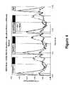
- FIG. 4is a time-concentration plot of tetraethyloxysilane (TEOS) and silicon tetrafluoride (SiF 4 ) as measured for the process effluent from an upstream plasma enhanced chemical vapor deposition chamber that is operated according to alternative deposition and cleaning cycles.
- TEOStetraethyloxysilane
- SiF 4silicon tetrafluoride
- FIG. 5is a graph showing the IR signal responses measured for a first transmission path having non-electropolished inner surface, a second transmission path having moderately electropolished inner surface, and a third transmission path having highly electropolished inner surface, at various IR wavelengths.
- FIGS. 6 and 7are perspective views of semiconductor process systems comprising purge gas inlets for introducing a purge gas to remove particles from the interfacial spaces between the sampling region and the IR source as well as between the sampling region and the thermopile detector.
- FIG. 8is a perspective view of semiconductor process system comprising purge gas inlets for forming a sheath of purge gas around the particle-containing process effluent in the sampling region.
- thermopile detector systemsuseful for semiconductor process monitoring and control.
- semiconductor processis intended to be broadly construed to include any and all processing and unit operations involved in the manufacture of semiconductor products, as well as all operations involving treatment or processing of materials used in or produced by a semiconductor manufacturing facility, as well as all operations carried out in connection with the semiconductor manufacturing facility not involving active manufacturing (examples include conditioning of process equipment, purging of chemical delivery lines in preparation for operation, etch cleaning of process tool chambers, abatement of toxic or hazardous gases from effluents produced by the semiconductor manufacturing facility, etc.).
- the thermopile-based infrared monitoring system of the inventioncomprises an infrared (IR) radiation source, a sampling region for exposing a material of interest (e.g., a process gas) to IR radiation, and a thermopile detector for analyzing the IR radiation as transmitted through the material of interest.
- the sampling region in the broad practice of the inventionmay comprise any suitable compartment, passageway or chamber, in which the material to be analyzed is subjected to passage of IR light therethrough for the purpose of using its IR absorbance-determined output to generate control signal(s) for process monitoring and control.
- the thermopile detectorgenerates small voltages when exposed to IR light (or heat in the IR spectral regime). The output signal of the thermopile detector is proportional to the incident radiation on the detector.
- Thermopile detectors employed in the preferred practice of the present inventionmay have a multiple array of elements in each detector unit.
- one of the thermopile detector elementsis used as a reference, sensing IR light in a range in which substantially no absorption occurs (e.g., wavelength of 4.00 ⁇ 0.02 ⁇ m).
- the second thermopile detector elementis coated with a filter that senses IR energy in the spectral range of interest (such spectral range depending on the particular material to be monitored). Comparison of the differences in the voltages generated by the reference thermopile detector element and those generated by the thermopile detector active element(s) provides a concentration measurement.
- Detectors with up to 4 thermopile detector element arraysare commercially available. For example, in a 4-element detector unit, one detector element is employed as a reference and the remaining 3 detector elements are utilized for measurements in different spectral regions.
- thermopile IR detectorhas a minimum requirement for the IR radiation intensity, in order to effectively detect such IR radiation. Therefore, when the intensity of the IR radiation generated by the IR source remains constant, the L Total has to be maintained at a level that is equal to or smaller than a maximum limit L 0 in order to enable detection of the IR radiation by the thermopile IR detector. On the other hand, since the concentration of the IR-absorbing material of interest directly correlates to and is determined by L Material , maximization of L Material will maximize the signal strength of the measurement, which is especially important for detection and analysis of low concentration IR-absorbing materials.
- the present inventionachieves the goal of maximizing L Material while maintaining L Total at or below a maximum limit L 0 , by reducing or minimizing L Path , according to the following methods:
- the loss of radiation intensityis effectively reduced in comparison to that of a non-linear transmission path that requires multiple reflections and refractions of the IR radiation, as shown in FIGS. 1A and 1B .
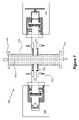
- the present inventionconstructs and arranges the IR radiation source, the sampling region, and the thermopile detector to provide a substantially linear transmission path for the IR light, as shown in FIG. 2 .
- the system 1comprises a sampling region 10 , preferably a gas sampling region having a gas inlet 12 and a gas outlet 14 and constitutes a part of a flow circuitry for flow of a process gas therethrough.
- the IR radiation source 20is positioned at one side of such gas sampling region 10 .
- the IR radiation source 20comprises an IR emitter 22 and a parabolic mirror 24 , for providing a parallel beam of IR light 2 , which is transmitted along a substantially linear transmission path through the gas sampling region 10 .
- the thermopile detector 40is positioned at the other side of such gas sampling region 10 for receiving and analyzing the transmitted IR light beam.
- the thermopile detector 40comprises an IR detecting element 44 having one or more IR radiation band pass filters for selectively transmitting a portion of the IR radiation of a narrow wavelength range that encompasses the absorption wavelength that is characteristic to the IR-absorbing component(s) of interest in the process gas, so that the decrease in output signal generated by such thermopile is directly related to the amount of infrared absorption by the corresponding component(s) of interest.
- the IR light beamis focused by a focusing lens 42 before entering the IR detecting element 44 .
- thermopile detector unitmay further include a multiplicity of absorber areas, including reference (unfiltered) absorber and gas-filtered absorber regions, with the latter filters being gas-specific for sensing of the semiconductor gases or gas components of interest (e.g., arsine, phosphine, germane, stibine, distibine, silane, substituted silanes, chlorine, bromine, organometallic precursor vapor, etc.).
- reference (unfiltered) absorbere.g., arsine, phosphine, germane, stibine, distibine, silane, substituted silanes, chlorine, bromine, organometallic precursor vapor, etc.
- the gas sampling region 10is separated from the IR radiation source 20 and the thermopile detector 40 by interfacial spaces 32 and 52 , which form parts of the IR transmission path.
- the interfacial space 32is connected to the IR radiation source 20 in a sealed manner, which comprises a weld connector 34 that is detachably and sealingly connected to the IR radiation source by a spacer 35 and O-rings 36 .
- the interfacial space 52is connected to the thermopile detector 40 in a sealed manner, which comprises a weld connector 54 that is detachably and sealingly connected to the IR radiation source by a spacer 55 and O-rings 56 .
- Such weld connector 34 and 54both comprise IR transparent materials and therefore form a portion of the IR transmission path.
- the linear transmission path of the IR radiationreduces unnecessary loss of radiation intensity.
- connection between the IR source, the gas sampling region, and the thermopile detectoris simple and robust, providing a sufficient small footprint and efficient resistance against misalignment.
- thermopile detector 40may be positioned behind the thermopile detector 40 , for immediately receiving output signals from the thermopile detector 40 , so as to further reduce the footprint and minimize signal loss due to remote connections.
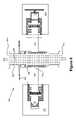
- the thermopile detector systemis utilized as an abatement tool controller for an abatement unit for treating process effluent produced in a semiconductor manufacturing operation, or other industrial process.
- the thermopile detector systemadvantageously is installed at the inlet of the abatement unit, where the abatement apparatus receives the effluent to be treated.
- the thermopile detector systemis used to sense whether or not an upstream tool that generates the effluent in active on-stream operation, is in an active operating mode, or alternatively whether or not the upstream tool is in a non-effluent-producing state, e.g., undergoing purging or cleaning.
- thermopile detector unitby way of specific example, is usefully employed as an abatement tool controller for an effluent scrubber, such as a wet/dry scrubber or a thermal scrubber, whereby the presence of the thermopile detector system transforms the scrubber into a “smart” scrubber and enhances the efficiency of the scrubber, allowing conservation of resources (lower consumables) to be achieved.
- effluent scrubbersuch as a wet/dry scrubber or a thermal scrubber
- FIG. 3shows a semiconductor process system 100 comprising a scrubber unit 140 having a gas inlet 142 and a gas outlet 144 .
- An IR source 120 and a thermopile detector 130are provided at both sides of a gas sampling region 110 near the gas inlet 142 of such scrubber unit 140 , for analyzing the composition of the effluent flowed into the scrubber.
- the output signal generated by the thermopile detector 130is forwarded through transmission line 152 to a microcontroller 150 .
- the microcontroller 150is connected to the scrubbing medium sources 160 and responsively adjusts the amount of scrubbing media (preferably fuel, water, and chemical additives) 162 , 164 , and 166 input according to the composition of the effluent as measured.
- scrubbing mediapreferably fuel, water, and chemical additives
- thermopile detector systemof the present invention.
- abatable components in the effluentincluding but not limited to, tetraethyloxysilane, silane, silicon tetrafluoride, silicon-containing organic compounds, boranes, arsenic hydride, phosphine, hydrogen fluoride, fluorine, tungsten hexafluoride, hydrogen chloride, chlorine, titanium tetrachloride, perfluorocarbons, nitrous oxide, ammonium, hydrogen, oxygen, argon, and helium, may be analyzed by the thermopile detector system of the present invention.
- Additional sensorssuch as temperature sensors, flow sensors, pressure transducers, ultraviolet spectrometers, mass spectrometers, and electrochemical sensors, may be provided for further measuring the flow rate, gas composition and concentration, pressure, and temperature of the effluent, so as to allow corresponding adjustment of the operational mode of the scrubber unit.
- the IR thermopile detector system of the present inventionmay be used to analyze the effluent gas species emitted from a plasma enhanced chemical vapor deposition (PECVD) chamber, in which SiO 2 films are deposited using tetraethyloxysilane (TEOS) and which performs chamber cleaning by using SiF 4 after each deposition cycle. Therefore, during the deposition cycles, the IR detector system measures the real-time concentration of TEOS in the deposition effluent. During alternating cleaning cycles, the IR detector system measures the SiF 4 concentration. Measurements obtained by the IR detector system during the alternating deposition/cleaning cycles are provided in FIG. 4 . The information collected by the IR photometer can be used to adjust the settings of the downstream scrubber unit for abatement of TEOS and SiF 4 .
- PECVDplasma enhanced chemical vapor deposition
- TEOStetraethyloxysilane
- a transmission path with a smooth, reflective inner faceis provided, which minimize the absorption and dissipation of IR radiation by the surface of such transmission path.
- such inner surface of the transmission pathis characterized by a roughness in a range of from about 0.012 ⁇ m Ra to about 1.80 ⁇ m Ra, more preferably from about 0.10 ⁇ m Ra to about 0.80 ⁇ m Ra, and most preferably from about 0.10 ⁇ m Ra to about 0.20 ⁇ m Ra.
- Such inner surfacemay further be characterized by a reflectivity in a range of from about 70% to about 99%, preferably from about 92% to about 97%.
- Such smooth, reflective inner surfacemay be provided by electropolishing or super polishing techniques.
- the path length for each transmission pathis the same, and the same IR source and thermopile detector are used.
- the measurement resultsindicate that the highly polished transmission path provides much stronger signal strength than that of the moderately polished and non-polished transmission paths.
- Process gas that contains particles or is susceptible to particles formationmay form particle deposits along the transmission path of the IR radiation, which will absorb the IR radiation and significantly reduces the radiation intensity of the IR radiation transmitted.
- the present inventiontherefore provides a purge gas near the interfacial spaces between the gas sampling region and the IR source as well as between the gas sampling region and the thermopile detector.
- the purge gas flowprovides a sufficient force to remove the particle deposits away from the IR source and the thermopile detector, so as to prevent such particles from interfering with the detection process.
- FIG. 6shows a gas sampling region 210 having an inlet 212 and an outlet 214 for flowing a particle-containing process gas 202 therethrough.
- An IR source 220is positioned at one side of such gas sampling region 210 and is isolated therefrom by an interfacial space 232
- a thermopile detector 240is positioned at the other side of such gas sampling region 210 and is isolated therefrom by an interfacial space 252 .
- a purge gas 262is introduced into such interfacial spaces 232 and 252 from a purge gas source (not shown), preferably through a porous media 264 , for forming a uniform flow of purge gas that moves away from the IR source 220 and the thermopile detector 240 toward the gas sampling region 210 .
- Such flow of purge gasfurther generates vacuum at the dead-end spaces near the IR source 220 and the thermopile detector 240 , so as to force the particle deposits out of such dead-end spaces and discharge same into the process gas flow in the gas sampling region 210 .
- the purge gasmay be introduced into the interfacial spaces 232 and 252 along a direction that is substantially parallel to the process gas flow, as shown in FIG. 6 , which then flows through such interfacial spaces into the gas sampling region 210 in a direction that is substantially perpendicular to the process gas flow.
- FIG. 7shows an alternative embodiment of the present invention, in which the purge gas is introduced into the interfacial spaces 332 and 352 in a direction that is substantially perpendicular to the process gas flow and flows through such interfacial spaces along the same direction into to the gas sampling region 210 .
- the purge gasmay be provided to form a gas sheath surrounding the process gas flow, so as to prevent particles from escaping from the gas sampling region.
- FIG. 8shows a purge gas 362 that forms an annular sheath 466 around the particle-containing process gas flow. Such purge gas is flowed in a direction that is confluent with the process gas flow and is therefore discharged of the gas sampling region 410 together with the process gas.
- external heating devicescan be provided for heating at least a portion of the IR transmission path (including the IR transmission windows), so as to generate a thermal gradient or heat flux, which functions to prevent the particles from accessing and depositing on the internal surface of the IR transmission path.
Landscapes
- Physics & Mathematics (AREA)
- General Physics & Mathematics (AREA)
- Spectroscopy & Molecular Physics (AREA)
- Engineering & Computer Science (AREA)
- Power Engineering (AREA)
- Microelectronics & Electronic Packaging (AREA)
- Computer Hardware Design (AREA)
- Manufacturing & Machinery (AREA)
- Chemical & Material Sciences (AREA)
- Life Sciences & Earth Sciences (AREA)
- Pathology (AREA)
- General Health & Medical Sciences (AREA)
- Condensed Matter Physics & Semiconductors (AREA)
- Biochemistry (AREA)
- Analytical Chemistry (AREA)
- Immunology (AREA)
- Health & Medical Sciences (AREA)
- Investigating Or Analysing Materials By Optical Means (AREA)
- Chemical Vapour Deposition (AREA)
- Photometry And Measurement Of Optical Pulse Characteristics (AREA)
- Radiation Pyrometers (AREA)
- Measuring Temperature Or Quantity Of Heat (AREA)
Abstract
Description
LTotal=LPath+LMaterial
Claims (20)
Priority Applications (1)
| Application Number | Priority Date | Filing Date | Title |
|---|---|---|---|
| US12/060,686US7723685B2 (en) | 2002-05-08 | 2008-04-01 | Monitoring system comprising infrared thermopile detector |
Applications Claiming Priority (5)
| Application Number | Priority Date | Filing Date | Title |
|---|---|---|---|
| US10/140,848US6617175B1 (en) | 2002-05-08 | 2002-05-08 | Infrared thermopile detector system for semiconductor process monitoring and control |
| US10/623,244US7011614B2 (en) | 2002-05-08 | 2003-07-18 | Infrared thermopile detector system for semiconductor process monitoring and control |
| US10/668,489US7129519B2 (en) | 2002-05-08 | 2003-09-23 | Monitoring system comprising infrared thermopile detector |
| US11/555,094US7351976B2 (en) | 2002-05-08 | 2006-10-31 | Monitoring system comprising infrared thermopile detector |
| US12/060,686US7723685B2 (en) | 2002-05-08 | 2008-04-01 | Monitoring system comprising infrared thermopile detector |
Related Parent Applications (1)
| Application Number | Title | Priority Date | Filing Date |
|---|---|---|---|
| US11/555,094ContinuationUS7351976B2 (en) | 2002-05-08 | 2006-10-31 | Monitoring system comprising infrared thermopile detector |
Publications (2)
| Publication Number | Publication Date |
|---|---|
| US20090039266A1 US20090039266A1 (en) | 2009-02-12 |
| US7723685B2true US7723685B2 (en) | 2010-05-25 |
Family
ID=27788466
Family Applications (6)
| Application Number | Title | Priority Date | Filing Date |
|---|---|---|---|
| US10/140,848Expired - LifetimeUS6617175B1 (en) | 2002-05-08 | 2002-05-08 | Infrared thermopile detector system for semiconductor process monitoring and control |
| US10/623,244Expired - LifetimeUS7011614B2 (en) | 2002-05-08 | 2003-07-18 | Infrared thermopile detector system for semiconductor process monitoring and control |
| US10/731,355Expired - LifetimeUS7172918B2 (en) | 2002-05-08 | 2003-12-09 | Infrared thermopile detector system for semiconductor process monitoring and control |
| US10/731,763Expired - LifetimeUS6821795B2 (en) | 2002-05-08 | 2003-12-09 | Infrared thermopile detector system for semiconductor process monitoring and control |
| US11/494,193AbandonedUS20060263916A1 (en) | 2002-05-08 | 2006-07-27 | Infrared thermopile detector system for semiconductor process monitoring and control |
| US12/060,686Expired - Fee RelatedUS7723685B2 (en) | 2002-05-08 | 2008-04-01 | Monitoring system comprising infrared thermopile detector |
Family Applications Before (5)
| Application Number | Title | Priority Date | Filing Date |
|---|---|---|---|
| US10/140,848Expired - LifetimeUS6617175B1 (en) | 2002-05-08 | 2002-05-08 | Infrared thermopile detector system for semiconductor process monitoring and control |
| US10/623,244Expired - LifetimeUS7011614B2 (en) | 2002-05-08 | 2003-07-18 | Infrared thermopile detector system for semiconductor process monitoring and control |
| US10/731,355Expired - LifetimeUS7172918B2 (en) | 2002-05-08 | 2003-12-09 | Infrared thermopile detector system for semiconductor process monitoring and control |
| US10/731,763Expired - LifetimeUS6821795B2 (en) | 2002-05-08 | 2003-12-09 | Infrared thermopile detector system for semiconductor process monitoring and control |
| US11/494,193AbandonedUS20060263916A1 (en) | 2002-05-08 | 2006-07-27 | Infrared thermopile detector system for semiconductor process monitoring and control |
Country Status (8)
| Country | Link |
|---|---|
| US (6) | US6617175B1 (en) |
| EP (1) | EP1502289A4 (en) |
| JP (1) | JP2005526406A (en) |
| KR (1) | KR100958464B1 (en) |
| CN (1) | CN1653588A (en) |
| AU (1) | AU2003276827A1 (en) |
| TW (1) | TWI296141B (en) |
| WO (1) | WO2004010462A2 (en) |
Cited By (3)
| Publication number | Priority date | Publication date | Assignee | Title |
|---|---|---|---|---|
| US20100217415A1 (en)* | 2003-03-28 | 2010-08-26 | Advanced Technology Materials, Inc. | Photometrically modulated delivery of reagents |
| US9340878B2 (en) | 2009-05-29 | 2016-05-17 | Entegris, Inc. | TPIR apparatus for monitoring tungsten hexafluoride processing to detect gas phase nucleation, and method and system utilizing same |
| US9506804B2 (en) | 2013-01-17 | 2016-11-29 | Detector Electronics Corporation | Open path gas detector |
Families Citing this family (51)
| Publication number | Priority date | Publication date | Assignee | Title |
|---|---|---|---|---|
| US6617175B1 (en)* | 2002-05-08 | 2003-09-09 | Advanced Technology Materials, Inc. | Infrared thermopile detector system for semiconductor process monitoring and control |
| US7129519B2 (en) | 2002-05-08 | 2006-10-31 | Advanced Technology Materials, Inc. | Monitoring system comprising infrared thermopile detector |
| US7080545B2 (en)* | 2002-10-17 | 2006-07-25 | Advanced Technology Materials, Inc. | Apparatus and process for sensing fluoro species in semiconductor processing systems |
| US6927393B2 (en)* | 2002-12-16 | 2005-08-09 | International Business Machines Corporation | Method of in situ monitoring of supercritical fluid process conditions |
| JP3705270B2 (en)* | 2003-01-20 | 2005-10-12 | セイコーエプソン株式会社 | Infrared absorption measurement method, infrared absorption measurement device, and semiconductor device manufacturing method |
| WO2004088415A2 (en)* | 2003-03-28 | 2004-10-14 | Advanced Technology Materials Inc. | Photometrically modulated delivery of reagents |
| GB0412623D0 (en)* | 2004-06-07 | 2004-07-07 | Boc Group Plc | Method controlling operation of a semiconductor processing system |
| US20060211253A1 (en)* | 2005-03-16 | 2006-09-21 | Ing-Shin Chen | Method and apparatus for monitoring plasma conditions in an etching plasma processing facility |
| DE102005015627A1 (en)* | 2005-04-06 | 2006-10-12 | Carl Zeiss Smt Ag | Optical imaging device |
| US20100224264A1 (en)* | 2005-06-22 | 2010-09-09 | Advanced Technology Materials, Inc. | Apparatus and process for integrated gas blending |
| US7735452B2 (en) | 2005-07-08 | 2010-06-15 | Mks Instruments, Inc. | Sensor for pulsed deposition monitoring and control |
| US7943204B2 (en) | 2005-08-30 | 2011-05-17 | Advanced Technology Materials, Inc. | Boron ion implantation using alternative fluorinated boron precursors, and formation of large boron hydrides for implantation |
| US7846131B2 (en) | 2005-09-30 | 2010-12-07 | Covidien Ag | Administration feeding set and flow control apparatus with secure loading features |
| US8021336B2 (en) | 2007-01-05 | 2011-09-20 | Tyco Healthcare Group Lp | Pump set for administering fluid with secure loading features and manufacture of component therefor |
| US7722573B2 (en)* | 2006-03-02 | 2010-05-25 | Covidien Ag | Pumping apparatus with secure loading features |
| US7758551B2 (en)* | 2006-03-02 | 2010-07-20 | Covidien Ag | Pump set with secure loading features |
| US7763005B2 (en) | 2006-03-02 | 2010-07-27 | Covidien Ag | Method for using a pump set having secure loading features |
| US7722562B2 (en) | 2006-03-02 | 2010-05-25 | Tyco Healthcare Group Lp | Pump set with safety interlock |
| US7927304B2 (en)* | 2006-03-02 | 2011-04-19 | Tyco Healthcare Group Lp | Enteral feeding pump and feeding set therefor |
| US20090175771A1 (en)* | 2006-03-16 | 2009-07-09 | Applied Materials, Inc. | Abatement of effluent gas |
| WO2007109082A2 (en)* | 2006-03-16 | 2007-09-27 | Applied Materials, Inc. | Methods and apparatus for improving operation of an electronic device manufacturing system |
| CN101400875B (en)* | 2006-03-16 | 2012-11-07 | 应用材料公司 | Method and apparatus for improved operation of an abatement system |
| US20080006775A1 (en)* | 2006-06-22 | 2008-01-10 | Arno Jose I | Infrared gas detection systems and methods |
| US20080241805A1 (en) | 2006-08-31 | 2008-10-02 | Q-Track Corporation | System and method for simulated dosimetry using a real time locating system |
| US7560686B2 (en)* | 2006-12-11 | 2009-07-14 | Tyco Healthcare Group Lp | Pump set and pump with electromagnetic radiation operated interlock |
| TW200846639A (en) | 2007-03-14 | 2008-12-01 | Entegris Inc | System and method for non-intrusive thermal monitor |
| CN101678407A (en)* | 2007-05-25 | 2010-03-24 | 应用材料股份有限公司 | Method and apparatus for efficient operation of an abatement system |
| WO2008156687A1 (en)* | 2007-06-15 | 2008-12-24 | Applied Materials, Inc. | Methods and systems for designing and validating operation of abatement systems |
| WO2009055750A1 (en) | 2007-10-26 | 2009-04-30 | Applied Materials, Inc. | Methods and apparatus for smart abatement using an improved fuel circuit |
| KR101755970B1 (en) | 2008-02-11 | 2017-07-07 | 엔테그리스, 아이엔씨. | Method of improving performance and extending lifetime of ion implant system including ion source chamber |
| US8401604B2 (en)* | 2008-04-11 | 2013-03-19 | Glucovista, Llc | Apparatus and methods for non-invasive measurement of a substance within a body |
| US8795225B2 (en)* | 2008-09-29 | 2014-08-05 | Covidien Lp | Fluid detection in an enteral feeding set |
| CN102177576B (en)* | 2008-10-08 | 2013-12-18 | 应用材料公司 | Method and device for detecting idle mode of processing equipment |
| US20110021011A1 (en) | 2009-07-23 | 2011-01-27 | Advanced Technology Materials, Inc. | Carbon materials for carbon implantation |
| US8598022B2 (en) | 2009-10-27 | 2013-12-03 | Advanced Technology Materials, Inc. | Isotopically-enriched boron-containing compounds, and methods of making and using same |
| JP5938350B2 (en)* | 2009-12-09 | 2016-06-22 | コーニンクレッカ フィリップス エヌ ヴェKoninklijke Philips N.V. | Gas measurement module |
| US20110220342A1 (en)* | 2010-03-12 | 2011-09-15 | Applied Materials, Inc. | Methods and apparatus for selectively reducing flow of coolant in a processing system |
| US8154274B2 (en) | 2010-05-11 | 2012-04-10 | Tyco Healthcare Group Lp | Safety interlock |
| DE102013202895A1 (en)* | 2013-02-22 | 2014-08-28 | Zf Friedrichshafen Ag | Multi-speed transmission in planetary construction |
| DE102013111790A1 (en)* | 2013-10-25 | 2015-04-30 | Aixtron Se | Energy and material consumption optimized CVD reactor |
| US20150187562A1 (en)* | 2013-12-27 | 2015-07-02 | Taiwan Semiconductor Manufacturing Company Ltd. | Abatement water flow control system and operation method thereof |
| US10066981B2 (en)* | 2015-04-29 | 2018-09-04 | Kpr U.S., Llc | Detection of malfunction of flow monitoring system of flow control apparatus |
| US9735069B2 (en)* | 2015-09-23 | 2017-08-15 | Lam Research Corporation | Method and apparatus for determining process rate |
| JP2017090351A (en)* | 2015-11-13 | 2017-05-25 | 株式会社堀場製作所 | Radiation thermometer |
| US10586744B2 (en)* | 2017-03-24 | 2020-03-10 | Applied Materials, Inc. | Method for optimizing dry absorber efficiency and lifetime in epitaxial applications |
| SG11202002893PA (en)* | 2017-10-12 | 2020-04-29 | Agency Science Tech & Res | Chemical sensor and method of forming the same |
| US10784174B2 (en) | 2017-10-13 | 2020-09-22 | Lam Research Corporation | Method and apparatus for determining etch process parameters |
| JP7175782B2 (en)* | 2019-01-25 | 2022-11-21 | 株式会社東芝 | Silicon-containing material forming device |
| JP7156605B2 (en)* | 2019-01-25 | 2022-10-19 | 株式会社東芝 | Processing equipment and processing method |
| US12368024B2 (en) | 2021-04-09 | 2025-07-22 | Applied Materials, Inc. | Methods and apparatus for processing a substrate |
| WO2025072547A1 (en)* | 2023-09-29 | 2025-04-03 | Lam Research Corporation | Chemical sensor for automatic flow compensation of mass flow controller |
Citations (39)
| Publication number | Priority date | Publication date | Assignee | Title |
|---|---|---|---|---|
| US4647777A (en) | 1985-05-31 | 1987-03-03 | Ametrek, Inc. | Selective gas detector |
| US4816294A (en) | 1987-05-04 | 1989-03-28 | Midwest Research Institute | Method and apparatus for removing and preventing window deposition during photochemical vapor deposition (photo-CVD) processes |
| US4859859A (en)* | 1986-12-04 | 1989-08-22 | Cascadia Technology Corporation | Gas analyzers |
| US4935345A (en) | 1987-04-07 | 1990-06-19 | Arizona Board Of Regents | Implantable microelectronic biochemical sensor incorporating thin film thermopile |
| US5047352A (en) | 1985-05-20 | 1991-09-10 | Arch Development Corporation | Selective chemical detection by energy modulation of sensors |
| US5262645A (en)* | 1991-09-03 | 1993-11-16 | General Motors Corporation | Sensor for measuring alcohol content of alcohol gasoline fuel mixtures |
| US5282473A (en) | 1992-11-10 | 1994-02-01 | Critikon, Inc. | Sidestream infrared gas analyzer requiring small sample volumes |
| US5367167A (en) | 1991-09-30 | 1994-11-22 | Texas Instruments Incorporated | Uncooled infrared detector and method for forming the same |
| US5404125A (en) | 1991-07-19 | 1995-04-04 | Terumo Kabushiki Kaisha | Infrared radiation sensor |
| US5464983A (en) | 1994-04-05 | 1995-11-07 | Industrial Scientific Corporation | Method and apparatus for determining the concentration of a gas |
| US5589689A (en) | 1994-07-07 | 1996-12-31 | Vaisala Oy | Infrared detector with Fabry-Perot interferometer |
| US5594248A (en) | 1993-02-25 | 1997-01-14 | Nec Corporation | Infrared imaging device and infrared imaging system using same |
| US5650624A (en) | 1995-04-13 | 1997-07-22 | Engelhard Sensor Technologies, Inc. | Passive infrared analysis gas sensor |
| US5721430A (en) | 1995-04-13 | 1998-02-24 | Engelhard Sensor Technologies Inc. | Passive and active infrared analysis gas sensors and applicable multichannel detector assembles |
| US5782974A (en) | 1994-02-02 | 1998-07-21 | Applied Materials, Inc. | Method of depositing a thin film using an optical pyrometer |
| US5834777A (en) | 1994-02-14 | 1998-11-10 | Telaire Systems, Inc. | NDIR gas sensor |
| US5932877A (en)* | 1997-04-17 | 1999-08-03 | Square One Technology, Inc. | High performance side stream infrared gas analyzer |
| US5962854A (en) | 1996-06-12 | 1999-10-05 | Ishizuka Electronics Corporation | Infrared sensor and infrared detector |
| US5967992A (en) | 1998-06-03 | 1999-10-19 | Trutex, Inc. | Radiometric temperature measurement based on empirical measurements and linear functions |
| US6045257A (en) | 1996-10-25 | 2000-04-04 | Exergen Corporation | Axillary infrared thermometer and method of use |
| US6122042A (en) | 1997-02-07 | 2000-09-19 | Wunderman; Irwin | Devices and methods for optically identifying characteristics of material objects |
| US6348650B1 (en) | 1999-03-24 | 2002-02-19 | Ishizuka Electronics Corporation | Thermopile infrared sensor and process for producing the same |
| US6370950B1 (en) | 1998-03-20 | 2002-04-16 | Berkin B.V. | Medium flow meter |
| US20020049389A1 (en) | 1996-09-04 | 2002-04-25 | Abreu Marcio Marc | Noninvasive measurement of chemical substances |
| US20020051132A1 (en) | 2000-03-31 | 2002-05-02 | Hiromoto Ohno | Measuring method for concentration of halogen and fluorine compound, measuring equipment thereof and manufacturing method of halogen compound |
| US6444474B1 (en) | 1998-04-22 | 2002-09-03 | Eltron Research, Inc. | Microfluidic system for measurement of total organic carbon |
| US6469303B1 (en) | 2000-05-17 | 2002-10-22 | Rae Systems, Inc. | Non-dispersive infrared gas sensor |
| US20020168289A1 (en) | 2001-05-11 | 2002-11-14 | Mcvey Iain F. | Non-dispersive mid-infrared sensor for vaporized hydrogen peroxide |
| US6617175B1 (en) | 2002-05-08 | 2003-09-09 | Advanced Technology Materials, Inc. | Infrared thermopile detector system for semiconductor process monitoring and control |
| US6649994B2 (en) | 2000-08-24 | 2003-11-18 | Heetronix | Temperature sensing system with matched temperature coefficients of expansion |
| US6694800B2 (en) | 2002-03-22 | 2004-02-24 | Instrumentarium Corp. | Gas analyzer using thermal detectors |
| US20040038442A1 (en) | 2002-08-26 | 2004-02-26 | Kinsman Larry D. | Optically interactive device packages and methods of assembly |
| US6828172B2 (en) | 2002-02-04 | 2004-12-07 | Delphi Technologies, Inc. | Process for a monolithically-integrated micromachined sensor and circuit |
| US6909093B2 (en) | 2001-03-16 | 2005-06-21 | Seiko Epson Corporation | Infrared detecting element, method of manufacturing the same and temperature measuring device |
| US20050211555A1 (en) | 2002-02-14 | 2005-09-29 | Solus Biosystems, Inc. | Method for multiple sample screening using IR spectroscopy |
| US7009267B2 (en) | 2003-09-01 | 2006-03-07 | Sharp Kabushiki Kaisha | Semiconductor device |
| US7033542B2 (en) | 2002-02-14 | 2006-04-25 | Archibald William B | High throughput screening with parallel vibrational spectroscopy |
| US20060219923A1 (en) | 2005-03-30 | 2006-10-05 | Denso Corporation | Infrared gas detector |
| US7129519B2 (en) | 2002-05-08 | 2006-10-31 | Advanced Technology Materials, Inc. | Monitoring system comprising infrared thermopile detector |
Family Cites Families (20)
| Publication number | Priority date | Publication date | Assignee | Title |
|---|---|---|---|---|
| US5341214A (en)* | 1989-09-06 | 1994-08-23 | Gaztech International Corporation | NDIR gas analysis using spectral ratioing technique |
| JPH0412525A (en)* | 1990-05-02 | 1992-01-17 | Babcock Hitachi Kk | Chemical vapor growth device for organic metal |
| US5100479A (en)* | 1990-09-21 | 1992-03-31 | The Board Of Regents Acting For And On Behalf Of The University Of Michigan | Thermopile infrared detector with semiconductor supporting rim |
| US5646983A (en)* | 1993-03-25 | 1997-07-08 | U.S. Robotics Access Corp. | Host computer digital signal processing system for communicating over voice-grade telephone channels |
| US5436457A (en)* | 1993-06-10 | 1995-07-25 | Horiba, Ltd. | Infrared gas analyzer |
| DE69425817D1 (en)* | 1994-06-04 | 2000-10-12 | Orbisphere Lab | Device and method for luminance analysis |
| JPH08153685A (en)* | 1994-11-25 | 1996-06-11 | Mitsubishi Corp | Special material gas supply device for semiconductors |
| US5649985A (en)* | 1995-11-29 | 1997-07-22 | Kanken Techno Co., Ltd. | Apparatus for removing harmful substances of exhaust gas discharged from semiconductor manufacturing process |
| JP3233059B2 (en)* | 1997-03-07 | 2001-11-26 | 株式会社村田製作所 | Ultrasonic sensor |
| US6067840A (en)* | 1997-08-04 | 2000-05-30 | Texas Instruments Incorporated | Method and apparatus for infrared sensing of gas |
| JP3699593B2 (en) | 1998-07-07 | 2005-09-28 | 弘昭 杉山 | Cleaning device |
| JP4245714B2 (en) | 1998-12-25 | 2009-04-02 | シーケーディ株式会社 | Exhaust switching device |
| US6396056B1 (en)* | 1999-07-08 | 2002-05-28 | Air Instruments And Measurements, Inc. | Gas detectors and gas analyzers utilizing spectral absorption |
| CA2316059A1 (en)* | 1999-08-24 | 2001-02-24 | Virgilio C. Go Boncan | Methods and compositions for use in cementing in cold environments |
| US6442736B1 (en)* | 2000-10-03 | 2002-08-27 | L'air Liquide Societe Anonyme A Directoire Et Conseil De Surveillance Pour L'etude Et L'expolitation Des Procedes Georges Claude | Semiconductor processing system and method for controlling moisture level therein |
| US6616753B2 (en)* | 2001-12-11 | 2003-09-09 | Halliburton Energy Services, Inc. | Methods and compositions for sealing subterranean zones |
| TW200407995A (en)* | 2002-11-08 | 2004-05-16 | Nanya Technology Corp | Mark and method for multiple alignment |
| US6989057B2 (en)* | 2002-12-10 | 2006-01-24 | Halliburton Energy Services, Inc. | Zeolite-containing cement composition |
| US6964302B2 (en)* | 2002-12-10 | 2005-11-15 | Halliburton Energy Services, Inc. | Zeolite-containing cement composition |
| US7544640B2 (en)* | 2002-12-10 | 2009-06-09 | Halliburton Energy Services, Inc. | Zeolite-containing treating fluid |
- 2002
- 2002-05-08USUS10/140,848patent/US6617175B1/ennot_activeExpired - Lifetime
- 2003
- 2003-04-28TWTW092109889Apatent/TWI296141B/ennot_activeIP Right Cessation
- 2003-05-05JPJP2004522955Apatent/JP2005526406A/enactivePending
- 2003-05-05CNCNA038104504Apatent/CN1653588A/enactivePending
- 2003-05-05WOPCT/US2003/013937patent/WO2004010462A2/enactiveSearch and Examination
- 2003-05-05EPEP03765426Apatent/EP1502289A4/ennot_activeWithdrawn
- 2003-05-05AUAU2003276827Apatent/AU2003276827A1/ennot_activeAbandoned
- 2003-05-05KRKR1020047017524Apatent/KR100958464B1/ennot_activeExpired - Fee Related
- 2003-07-18USUS10/623,244patent/US7011614B2/ennot_activeExpired - Lifetime
- 2003-12-09USUS10/731,355patent/US7172918B2/ennot_activeExpired - Lifetime
- 2003-12-09USUS10/731,763patent/US6821795B2/ennot_activeExpired - Lifetime
- 2006
- 2006-07-27USUS11/494,193patent/US20060263916A1/ennot_activeAbandoned
- 2008
- 2008-04-01USUS12/060,686patent/US7723685B2/ennot_activeExpired - Fee Related
Patent Citations (44)
| Publication number | Priority date | Publication date | Assignee | Title |
|---|---|---|---|---|
| US5047352A (en) | 1985-05-20 | 1991-09-10 | Arch Development Corporation | Selective chemical detection by energy modulation of sensors |
| US4647777A (en) | 1985-05-31 | 1987-03-03 | Ametrek, Inc. | Selective gas detector |
| US4859859A (en)* | 1986-12-04 | 1989-08-22 | Cascadia Technology Corporation | Gas analyzers |
| US4935345A (en) | 1987-04-07 | 1990-06-19 | Arizona Board Of Regents | Implantable microelectronic biochemical sensor incorporating thin film thermopile |
| US4816294A (en) | 1987-05-04 | 1989-03-28 | Midwest Research Institute | Method and apparatus for removing and preventing window deposition during photochemical vapor deposition (photo-CVD) processes |
| US5404125A (en) | 1991-07-19 | 1995-04-04 | Terumo Kabushiki Kaisha | Infrared radiation sensor |
| US5262645A (en)* | 1991-09-03 | 1993-11-16 | General Motors Corporation | Sensor for measuring alcohol content of alcohol gasoline fuel mixtures |
| US5367167A (en) | 1991-09-30 | 1994-11-22 | Texas Instruments Incorporated | Uncooled infrared detector and method for forming the same |
| US5282473A (en) | 1992-11-10 | 1994-02-01 | Critikon, Inc. | Sidestream infrared gas analyzer requiring small sample volumes |
| US5594248A (en) | 1993-02-25 | 1997-01-14 | Nec Corporation | Infrared imaging device and infrared imaging system using same |
| US5782974A (en) | 1994-02-02 | 1998-07-21 | Applied Materials, Inc. | Method of depositing a thin film using an optical pyrometer |
| US5834777A (en) | 1994-02-14 | 1998-11-10 | Telaire Systems, Inc. | NDIR gas sensor |
| US5464983A (en) | 1994-04-05 | 1995-11-07 | Industrial Scientific Corporation | Method and apparatus for determining the concentration of a gas |
| US5589689A (en) | 1994-07-07 | 1996-12-31 | Vaisala Oy | Infrared detector with Fabry-Perot interferometer |
| US5650624A (en) | 1995-04-13 | 1997-07-22 | Engelhard Sensor Technologies, Inc. | Passive infrared analysis gas sensor |
| US5721430A (en) | 1995-04-13 | 1998-02-24 | Engelhard Sensor Technologies Inc. | Passive and active infrared analysis gas sensors and applicable multichannel detector assembles |
| US5962854A (en) | 1996-06-12 | 1999-10-05 | Ishizuka Electronics Corporation | Infrared sensor and infrared detector |
| US20020049389A1 (en) | 1996-09-04 | 2002-04-25 | Abreu Marcio Marc | Noninvasive measurement of chemical substances |
| US6045257A (en) | 1996-10-25 | 2000-04-04 | Exergen Corporation | Axillary infrared thermometer and method of use |
| US6122042A (en) | 1997-02-07 | 2000-09-19 | Wunderman; Irwin | Devices and methods for optically identifying characteristics of material objects |
| US5932877A (en)* | 1997-04-17 | 1999-08-03 | Square One Technology, Inc. | High performance side stream infrared gas analyzer |
| US6370950B1 (en) | 1998-03-20 | 2002-04-16 | Berkin B.V. | Medium flow meter |
| US6444474B1 (en) | 1998-04-22 | 2002-09-03 | Eltron Research, Inc. | Microfluidic system for measurement of total organic carbon |
| US5967992A (en) | 1998-06-03 | 1999-10-19 | Trutex, Inc. | Radiometric temperature measurement based on empirical measurements and linear functions |
| US6348650B1 (en) | 1999-03-24 | 2002-02-19 | Ishizuka Electronics Corporation | Thermopile infrared sensor and process for producing the same |
| US20020051132A1 (en) | 2000-03-31 | 2002-05-02 | Hiromoto Ohno | Measuring method for concentration of halogen and fluorine compound, measuring equipment thereof and manufacturing method of halogen compound |
| US6469303B1 (en) | 2000-05-17 | 2002-10-22 | Rae Systems, Inc. | Non-dispersive infrared gas sensor |
| US6649994B2 (en) | 2000-08-24 | 2003-11-18 | Heetronix | Temperature sensing system with matched temperature coefficients of expansion |
| US6909093B2 (en) | 2001-03-16 | 2005-06-21 | Seiko Epson Corporation | Infrared detecting element, method of manufacturing the same and temperature measuring device |
| US20020168289A1 (en) | 2001-05-11 | 2002-11-14 | Mcvey Iain F. | Non-dispersive mid-infrared sensor for vaporized hydrogen peroxide |
| US6828172B2 (en) | 2002-02-04 | 2004-12-07 | Delphi Technologies, Inc. | Process for a monolithically-integrated micromachined sensor and circuit |
| US7033542B2 (en) | 2002-02-14 | 2006-04-25 | Archibald William B | High throughput screening with parallel vibrational spectroscopy |
| US20050211555A1 (en) | 2002-02-14 | 2005-09-29 | Solus Biosystems, Inc. | Method for multiple sample screening using IR spectroscopy |
| US6694800B2 (en) | 2002-03-22 | 2004-02-24 | Instrumentarium Corp. | Gas analyzer using thermal detectors |
| US6821795B2 (en) | 2002-05-08 | 2004-11-23 | Advanced Technology Materials, Inc. | Infrared thermopile detector system for semiconductor process monitoring and control |
| US7011614B2 (en) | 2002-05-08 | 2006-03-14 | Advanced Technology Materials, Inc. | Infrared thermopile detector system for semiconductor process monitoring and control |
| US6617175B1 (en) | 2002-05-08 | 2003-09-09 | Advanced Technology Materials, Inc. | Infrared thermopile detector system for semiconductor process monitoring and control |
| US7129519B2 (en) | 2002-05-08 | 2006-10-31 | Advanced Technology Materials, Inc. | Monitoring system comprising infrared thermopile detector |
| US20060263916A1 (en) | 2002-05-08 | 2006-11-23 | Jose Arno | Infrared thermopile detector system for semiconductor process monitoring and control |
| US7172918B2 (en) | 2002-05-08 | 2007-02-06 | Advanced Technology Materials, Inc. | Infrared thermopile detector system for semiconductor process monitoring and control |
| US7351976B2 (en) | 2002-05-08 | 2008-04-01 | Advanced Technology Materials, Inc. | Monitoring system comprising infrared thermopile detector |
| US20040038442A1 (en) | 2002-08-26 | 2004-02-26 | Kinsman Larry D. | Optically interactive device packages and methods of assembly |
| US7009267B2 (en) | 2003-09-01 | 2006-03-07 | Sharp Kabushiki Kaisha | Semiconductor device |
| US20060219923A1 (en) | 2005-03-30 | 2006-10-05 | Denso Corporation | Infrared gas detector |
Non-Patent Citations (5)
| Title |
|---|
| Adrian, Peter, "Sensor industry developments and trends", "Sensor Business Digest", Oct. 2001, Publisher: Vital Information Publication. |
| IEEE, "The Authoritative Dictionary of IEEE Standard Terms, Seventh Edition", Jan. 2001, p. 1174 Publisher: The Institute of Electrical and Electronics Engineers, Inc. |
| Schilz, Jurgen, "Applications of thermoelectric infrared sensors (thermopiles): Gas detection by infrared absorption; NDIR", "Thermophysica Minima", Aug. 22, 2000, Publisher: PerkinElmer. |
| Thermometrics Global Business, "Application note of thermopile sensors (Rev.02)", 2000, pp. 1-9. |
| Wilks, Paul A., "The birth of infrared filtometry", "Spectroscopy Showcase-www.spectroscopyonline.com", Mar. 2002, pp. 14. |
Cited By (5)
| Publication number | Priority date | Publication date | Assignee | Title |
|---|---|---|---|---|
| US20100217415A1 (en)* | 2003-03-28 | 2010-08-26 | Advanced Technology Materials, Inc. | Photometrically modulated delivery of reagents |
| US7925450B2 (en) | 2003-03-28 | 2011-04-12 | Advanced Technology Materials, Inc. | Photometrically modulated delivery of reagents |
| US8244482B2 (en) | 2003-03-28 | 2012-08-14 | Advanced Technology Materials, Inc. | Photometrically modulated delivery of reagents |
| US9340878B2 (en) | 2009-05-29 | 2016-05-17 | Entegris, Inc. | TPIR apparatus for monitoring tungsten hexafluoride processing to detect gas phase nucleation, and method and system utilizing same |
| US9506804B2 (en) | 2013-01-17 | 2016-11-29 | Detector Electronics Corporation | Open path gas detector |
Also Published As
| Publication number | Publication date |
|---|---|
| US20040018746A1 (en) | 2004-01-29 |
| WO2004010462A3 (en) | 2004-11-25 |
| US7011614B2 (en) | 2006-03-14 |
| US7172918B2 (en) | 2007-02-06 |
| US20090039266A1 (en) | 2009-02-12 |
| EP1502289A2 (en) | 2005-02-02 |
| KR20040108767A (en) | 2004-12-24 |
| US20060263916A1 (en) | 2006-11-23 |
| US20040121494A1 (en) | 2004-06-24 |
| TWI296141B (en) | 2008-04-21 |
| TW200401384A (en) | 2004-01-16 |
| US6617175B1 (en) | 2003-09-09 |
| AU2003276827A1 (en) | 2004-02-09 |
| EP1502289A4 (en) | 2010-01-20 |
| JP2005526406A (en) | 2005-09-02 |
| KR100958464B1 (en) | 2010-05-17 |
| WO2004010462A2 (en) | 2004-01-29 |
| AU2003276827A8 (en) | 2004-02-09 |
| US20040113080A1 (en) | 2004-06-17 |
| US6821795B2 (en) | 2004-11-23 |
| CN1653588A (en) | 2005-08-10 |
Similar Documents
| Publication | Publication Date | Title |
|---|---|---|
| US7723685B2 (en) | Monitoring system comprising infrared thermopile detector | |
| US7351976B2 (en) | Monitoring system comprising infrared thermopile detector | |
| JP6450850B2 (en) | Small volume, long path length multi-pass gas cell for monitoring infrared and ultraviolet radiation | |
| US6885452B2 (en) | Chamber effluent monitoring system and semiconductor processing system comprising absorption spectroscopy measurement system, and methods of use | |
| US6442736B1 (en) | Semiconductor processing system and method for controlling moisture level therein | |
| US5818578A (en) | Polygonal planar multipass cell, system and apparatus including same, and method of use | |
| US6421127B1 (en) | Method and system for preventing deposition on an optical component in a spectroscopic sensor | |
| US6188475B1 (en) | In-line cell for absorption spectroscopy | |
| US20020152797A1 (en) | Gas delivery apparatus and method for monitoring a gas phase species therein | |
| CN1283788A (en) | Method and appts for analyzing molecular sorts in vacuum by resonant wave and spectrum sensitivity | |
| WO1999064814A1 (en) | Method and apparatus for determining processing chamber cleaning or wafer etching endpoint | |
| CN1155655A (en) | Chamber effluent monitoring system and semiconductor processing system comprising absorption spectroscopy measurement system, and method of use |
Legal Events
| Date | Code | Title | Description |
|---|---|---|---|
| FEPP | Fee payment procedure | Free format text:PAYOR NUMBER ASSIGNED (ORIGINAL EVENT CODE: ASPN); ENTITY STATUS OF PATENT OWNER: LARGE ENTITY | |
| REMI | Maintenance fee reminder mailed | ||
| AS | Assignment | Owner name:GOLDMAN SACHS BANK USA, AS COLLATERAL AGENT, NEW YORK Free format text:SECURITY INTEREST;ASSIGNORS:ENTEGRIS, INC.;POCO GRAPHITE, INC.;ATMI, INC.;AND OTHERS;REEL/FRAME:032815/0852 Effective date:20140430 Owner name:GOLDMAN SACHS BANK USA, AS COLLATERAL AGENT, NEW Y Free format text:SECURITY INTEREST;ASSIGNORS:ENTEGRIS, INC.;POCO GRAPHITE, INC.;ATMI, INC.;AND OTHERS;REEL/FRAME:032815/0852 Effective date:20140430 | |
| AS | Assignment | Owner name:GOLDMAN SACHS BANK USA, AS COLLATERAL AGENT, NEW YORK Free format text:SECURITY INTEREST;ASSIGNORS:ENTEGRIS, INC.;POCO GRAPHITE, INC.;ATMI, INC.;AND OTHERS;REEL/FRAME:032812/0192 Effective date:20140430 Owner name:GOLDMAN SACHS BANK USA, AS COLLATERAL AGENT, NEW Y Free format text:SECURITY INTEREST;ASSIGNORS:ENTEGRIS, INC.;POCO GRAPHITE, INC.;ATMI, INC.;AND OTHERS;REEL/FRAME:032812/0192 Effective date:20140430 | |
| LAPS | Lapse for failure to pay maintenance fees | ||
| STCH | Information on status: patent discontinuation | Free format text:PATENT EXPIRED DUE TO NONPAYMENT OF MAINTENANCE FEES UNDER 37 CFR 1.362 | |
| FP | Lapsed due to failure to pay maintenance fee | Effective date:20140525 | |
| AS | Assignment | Owner name:POCO GRAPHITE, INC., MASSACHUSETTS Free format text:RELEASE BY SECURED PARTY;ASSIGNOR:GOLDMAN SACHS BANK USA, AS COLLATERAL AGENT;REEL/FRAME:047477/0032 Effective date:20181106 Owner name:ENTEGRIS, INC., MASSACHUSETTS Free format text:RELEASE BY SECURED PARTY;ASSIGNOR:GOLDMAN SACHS BANK USA, AS COLLATERAL AGENT;REEL/FRAME:047477/0032 Effective date:20181106 Owner name:ATMI, INC., CONNECTICUT Free format text:RELEASE BY SECURED PARTY;ASSIGNOR:GOLDMAN SACHS BANK USA, AS COLLATERAL AGENT;REEL/FRAME:047477/0032 Effective date:20181106 Owner name:ADVANCED TECHNOLOGY MATERIALS, INC., CONNECTICUT Free format text:RELEASE BY SECURED PARTY;ASSIGNOR:GOLDMAN SACHS BANK USA, AS COLLATERAL AGENT;REEL/FRAME:047477/0032 Effective date:20181106 Owner name:ATMI PACKAGING, INC., CONNECTICUT Free format text:RELEASE BY SECURED PARTY;ASSIGNOR:GOLDMAN SACHS BANK USA, AS COLLATERAL AGENT;REEL/FRAME:047477/0032 Effective date:20181106 Owner name:ATMI, INC., CONNECTICUT Free format text:RELEASE BY SECURED PARTY;ASSIGNOR:GOLDMAN SACHS BANK USA, AS COLLATERAL AGENT;REEL/FRAME:047477/0151 Effective date:20181106 Owner name:ATMI PACKAGING, INC., CONNECTICUT Free format text:RELEASE BY SECURED PARTY;ASSIGNOR:GOLDMAN SACHS BANK USA, AS COLLATERAL AGENT;REEL/FRAME:047477/0151 Effective date:20181106 Owner name:ADVANCED TECHNOLOGY MATERIALS, INC., CONNECTICUT Free format text:RELEASE BY SECURED PARTY;ASSIGNOR:GOLDMAN SACHS BANK USA, AS COLLATERAL AGENT;REEL/FRAME:047477/0151 Effective date:20181106 Owner name:POCO GRAPHITE, INC., MASSACHUSETTS Free format text:RELEASE BY SECURED PARTY;ASSIGNOR:GOLDMAN SACHS BANK USA, AS COLLATERAL AGENT;REEL/FRAME:047477/0151 Effective date:20181106 Owner name:ENTEGRIS, INC., MASSACHUSETTS Free format text:RELEASE BY SECURED PARTY;ASSIGNOR:GOLDMAN SACHS BANK USA, AS COLLATERAL AGENT;REEL/FRAME:047477/0151 Effective date:20181106 |