US7719876B2 - Preservation circuit and methods to maintain values representing data in one or more layers of memory - Google Patents
Preservation circuit and methods to maintain values representing data in one or more layers of memoryDownload PDFInfo
- Publication number
- US7719876B2 US7719876B2US12/221,136US22113608AUS7719876B2US 7719876 B2US7719876 B2US 7719876B2US 22113608 AUS22113608 AUS 22113608AUS 7719876 B2US7719876 B2US 7719876B2
- Authority
- US
- United States
- Prior art keywords
- memory
- power
- circuit
- preservation
- trigger
- Prior art date
- Legal status (The legal status is an assumption and is not a legal conclusion. Google has not performed a legal analysis and makes no representation as to the accuracy of the status listed.)
- Active, expires
Links
- 230000015654memoryEffects0.000titleclaimsabstractdescription403
- 238000004321preservationMethods0.000titleclaimsdescription155
- 238000000034methodMethods0.000titleabstractdescription40
- 239000000872bufferSubstances0.000claimsdescription20
- 230000004044responseEffects0.000claimsdescription5
- 230000001960triggered effectEffects0.000abstract1
- 239000010410layerSubstances0.000description36
- 238000010586diagramMethods0.000description15
- 238000005516engineering processMethods0.000description9
- 230000008569processEffects0.000description9
- 230000006870functionEffects0.000description8
- 239000003990capacitorSubstances0.000description7
- 238000007726management methodMethods0.000description6
- 230000014759maintenance of locationEffects0.000description5
- 239000002356single layerSubstances0.000description5
- 230000007958sleepEffects0.000description5
- 239000000758substrateSubstances0.000description5
- 238000004891communicationMethods0.000description4
- 230000005540biological transmissionEffects0.000description3
- 230000008859changeEffects0.000description3
- 239000004020conductorSubstances0.000description3
- 239000000470constituentSubstances0.000description3
- 238000004519manufacturing processMethods0.000description3
- 238000012986modificationMethods0.000description3
- 230000004048modificationEffects0.000description3
- BASFCYQUMIYNBI-UHFFFAOYSA-NplatinumChemical compound[Pt]BASFCYQUMIYNBI-UHFFFAOYSA-N0.000description3
- XUIMIQQOPSSXEZ-UHFFFAOYSA-NSiliconChemical compound[Si]XUIMIQQOPSSXEZ-UHFFFAOYSA-N0.000description2
- 230000008901benefitEffects0.000description2
- 238000013500data storageMethods0.000description2
- 230000005611electricityEffects0.000description2
- 230000007246mechanismEffects0.000description2
- 230000003287optical effectEffects0.000description2
- 230000009467reductionEffects0.000description2
- 230000000717retained effectEffects0.000description2
- 239000004065semiconductorSubstances0.000description2
- 230000011664signalingEffects0.000description2
- 229910052710siliconInorganic materials0.000description2
- 239000010703siliconSubstances0.000description2
- 230000003068static effectEffects0.000description2
- 239000004557technical materialSubstances0.000description2
- RYGMFSIKBFXOCR-UHFFFAOYSA-NCopperChemical compound[Cu]RYGMFSIKBFXOCR-UHFFFAOYSA-N0.000description1
- 238000003491arrayMethods0.000description1
- 230000006399behaviorEffects0.000description1
- 230000015556catabolic processEffects0.000description1
- 230000001413cellular effectEffects0.000description1
- 239000000919ceramicSubstances0.000description1
- 238000006243chemical reactionMethods0.000description1
- 238000004590computer programMethods0.000description1
- 239000013078crystalSubstances0.000description1
- 230000003247decreasing effectEffects0.000description1
- 230000007547defectEffects0.000description1
- 238000006731degradation reactionMethods0.000description1
- 230000001934delayEffects0.000description1
- 230000001066destructive effectEffects0.000description1
- 238000001514detection methodMethods0.000description1
- 238000009792diffusion processMethods0.000description1
- 239000000835fiberSubstances0.000description1
- 239000003292glueSubstances0.000description1
- 230000006266hibernationEffects0.000description1
- 238000012886linear functionMethods0.000description1
- 239000000463materialSubstances0.000description1
- 230000005055memory storageEffects0.000description1
- 239000002184metalSubstances0.000description1
- 229910052751metalInorganic materials0.000description1
- 230000000737periodic effectEffects0.000description1
- 229910052697platinumInorganic materials0.000description1
- 238000007639printingMethods0.000description1
- 238000004088simulationMethods0.000description1
- 230000000007visual effectEffects0.000description1
Images


Classifications
- G—PHYSICS
- G11—INFORMATION STORAGE
- G11C—STATIC STORES
- G11C13/00—Digital stores characterised by the use of storage elements not covered by groups G11C11/00, G11C23/00, or G11C25/00
- G11C13/0002—Digital stores characterised by the use of storage elements not covered by groups G11C11/00, G11C23/00, or G11C25/00 using resistive RAM [RRAM] elements
- G11C13/0021—Auxiliary circuits
- G11C13/0035—Evaluating degradation, retention or wearout, e.g. by counting writing cycles
- G—PHYSICS
- G11—INFORMATION STORAGE
- G11C—STATIC STORES
- G11C11/00—Digital stores characterised by the use of particular electric or magnetic storage elements; Storage elements therefor
- G11C11/02—Digital stores characterised by the use of particular electric or magnetic storage elements; Storage elements therefor using magnetic elements
- G11C11/16—Digital stores characterised by the use of particular electric or magnetic storage elements; Storage elements therefor using magnetic elements using elements in which the storage effect is based on magnetic spin effect
- G—PHYSICS
- G11—INFORMATION STORAGE
- G11C—STATIC STORES
- G11C13/00—Digital stores characterised by the use of storage elements not covered by groups G11C11/00, G11C23/00, or G11C25/00
- G11C13/0002—Digital stores characterised by the use of storage elements not covered by groups G11C11/00, G11C23/00, or G11C25/00 using resistive RAM [RRAM] elements
- G11C13/0021—Auxiliary circuits
- G11C13/0033—Disturbance prevention or evaluation; Refreshing of disturbed memory data
- G—PHYSICS
- G11—INFORMATION STORAGE
- G11C—STATIC STORES
- G11C13/00—Digital stores characterised by the use of storage elements not covered by groups G11C11/00, G11C23/00, or G11C25/00
- G11C13/0002—Digital stores characterised by the use of storage elements not covered by groups G11C11/00, G11C23/00, or G11C25/00 using resistive RAM [RRAM] elements
- G11C13/0021—Auxiliary circuits
- G11C13/004—Reading or sensing circuits or methods
- G—PHYSICS
- G11—INFORMATION STORAGE
- G11C—STATIC STORES
- G11C13/00—Digital stores characterised by the use of storage elements not covered by groups G11C11/00, G11C23/00, or G11C25/00
- G11C13/0002—Digital stores characterised by the use of storage elements not covered by groups G11C11/00, G11C23/00, or G11C25/00 using resistive RAM [RRAM] elements
- G11C13/0021—Auxiliary circuits
- G11C13/0061—Timing circuits or methods
- G—PHYSICS
- G11—INFORMATION STORAGE
- G11C—STATIC STORES
- G11C13/00—Digital stores characterised by the use of storage elements not covered by groups G11C11/00, G11C23/00, or G11C25/00
- G11C13/0002—Digital stores characterised by the use of storage elements not covered by groups G11C11/00, G11C23/00, or G11C25/00 using resistive RAM [RRAM] elements
- G11C13/0021—Auxiliary circuits
- G11C13/0069—Writing or programming circuits or methods
- G—PHYSICS
- G11—INFORMATION STORAGE
- G11C—STATIC STORES
- G11C5/00—Details of stores covered by group G11C11/00
- G11C5/02—Disposition of storage elements, e.g. in the form of a matrix array
- G—PHYSICS
- G11—INFORMATION STORAGE
- G11C—STATIC STORES
- G11C2213/00—Indexing scheme relating to G11C13/00 for features not covered by this group
- G11C2213/70—Resistive array aspects
- G11C2213/71—Three dimensional array
- G—PHYSICS
- G11—INFORMATION STORAGE
- G11C—STATIC STORES
- G11C2213/00—Indexing scheme relating to G11C13/00 for features not covered by this group
- G11C2213/70—Resistive array aspects
- G11C2213/77—Array wherein the memory element being directly connected to the bit lines and word lines without any access device being used
- G—PHYSICS
- G11—INFORMATION STORAGE
- G11C—STATIC STORES
- G11C5/00—Details of stores covered by group G11C11/00
- G11C5/005—Circuit means for protection against loss of information of semiconductor storage devices
Definitions
- the present inventionrelates generally to semiconductors and memory technology. More specifically, the present invention relates to data retention in non-volatile memory.
- a semiconductor memoryis generally considered to be one of two types of memory—volatile memory or nonvolatile memory.
- volatile memory technologiesgenerally have relatively lower storage densities and faster access times, as compared to nonvolatile memory technologies.
- volatile memory technologiestypically require a constant power source to retain the memory contents, unlike nonvolatile memory technologies, which do not generally require a constant power source.
- DRAMdynamic random access memory
- SRAMstatic random access memory
- a memory cell in a DRAM cellusually consists of a transistor and a capacitor to store a bit of data. Since capacitors typically leak electrical charge, a DRAM needs to be constantly refreshed to retain the memory contents. Electrical power is typically consumed to refresh a number of memory cells (e.g., every memory cell) in a DRAM, even if the memory or part of the memory is not being used.
- an SRAM cellusually includes several transistors implemented as a flip-flop to store each bit of memory.
- An SRAM cellis typically sensitive to power glitches, during which some or all of the memory contents are lost. Although an SRAM cell does not require refreshing, it commonly requires constant power to maintain its memory contents, even if the memory or part of the memory is not in use.
- Flash memorytypically uses complex logic, including state machines and other logic devices, to read and program a memory. Flash memory usually is slower than SRAM or DRAM since Flash memory includes a complex interface and requires erasing and/or programming in blocks of bits. However, Flash memory retains its contents when power is removed from (i.e., is not applied to) the memory.
- Flash memorymay be implemented as NOR and NAND Flash types.
- NOR Flashallows dynamic memory access (“DMA”) and, thus, is relatively faster than NAND Flash in accessing small amount of data.
- DMAdynamic memory access
- NOR Flashis slower than volatile memory, such as SRAM or DRAM.
- NAND Flashoffers higher densities on a given die size compared with NOR Flash.
- FIG. 1Adepicts an exemplary memory device, according to one or more embodiments of the invention.
- FIG. 1Bdepicts an alternative exemplary memory device with multiple layers of memory, according to one or more embodiments of the invention.
- FIG. 1Cdepicts an exemplary memory device with mixed memory configurations, according to one or more embodiments of the invention.
- FIG. 2Adepicts a block diagram of an exemplary trigger circuit, according to one or more embodiments of the invention.
- FIG. 2Bdepicts a block diagram of an exemplary preservation circuit, according to one or more embodiments of the invention.
- FIG. 3Adepicts an exemplary method of restoring memory, according to one or more embodiments of the invention.
- FIG. 3Bdepicts an alternative exemplary method of restoring memory, according to one or more embodiments of the invention.
- FIG. 4is a flow diagram depicting an exemplary method of restoring memory, according to one or more embodiments of the invention.
- FIG. 5depicts an exemplary memory device with an on-board power supply, according to one or more embodiments of the invention.
- a preservation circuitmay be configured to preserve values, such as parametric values, that represent the logic states for data (or a datum) stored in a memory that is composed of at least one layer of memory elements.
- parametric valuesinclude values that represent storage-related parameters of a memory element or cell, including, but not limited to voltages, currents, resistances, amounts of electrical charge (e.g., stored in association with a ferroelectric layer), magnetic fields (e.g., intensities or polarities thereof, such as in association with a Magnetoresistive Random Access Memory, or MRAM) or any other mechanism by which to write and/or read data (or a datum).
- a preservation circuitmay be used to ensure that a memory retains its data over a variety of conditions, including over time and over a reduction of power (e.g., during brown-out conditions, and/or absence of power).
- a preservation circuitconsider that a memory is fabricated with, for example, deviations in manufacturing parameters (e.g., deviations in process).
- One type of manufacturing defectmay cause degradation (e.g., leakage or drift) of a parametric value, such as a resistive value, which may corrupt the contents of a memory.
- a preservation circuitmay thereby enhance the data retention capabilities of a memory by preserving values that represent certain states of data, according to at least one embodiment.
- the memorymay include one or more layers of non-volatile memory elements.
- the memorymay be composed of memory elements having non-volatility characteristics for extended periods of time during which power is not applied to the memory elements storing the data.
- the term “power absence period”may refer, at least in one embodiment, to an amount of time over which a memory element or cell (or a collection thereof) exhibits non-volatility characteristics by maintaining its contents during the absence of power.
- a power absence periodmay be expressed in durations of, for example, milliseconds (e.g., 100 milliseconds or more, such as more than 500 milliseconds), seconds, minutes, hours, days, months, etc., as well as a number of access operations (e.g., number of write operations, or read operations).
- a non-volatile memorymay be characterized as having a power absence period over which it possesses non-volatile capabilities.
- one type of memorymay possess non-volatile capabilities for 90 days (e.g., at standard temperature, pressure, etc.), after which the probability increases that at least one memory cell in the memory might behave as a volatile memory cell.
- the term “non-volatile,” in terms of memorymay refer, at least in one embodiment, to the ability of memory to retain data stored therein during a reduction in or an absence of power, regardless of the power absence period associated with the memory.
- Memory elementsmay be two dimensional or three dimensional and may be arranged in a two-terminal or three-terminal memory array, in accordance with various embodiments of the invention.
- techniquessuch as those described herein enable emulation of multiple memory types for implementation on a single component such as a wafer, substrate, or die.
- U.S. patent application Ser. No. 11/095,026, filed Mar. 30, 2005 and entitled “Memory Using Mixed Valence Conductive Oxides,”is hereby incorporated by reference in its entirety for all purposes and describes non-volatile third dimensional memory elements that may be arranged in a two-terminal, cross-point memory array.
- Various memory structuresare possible with the implementation of the third dimensional memory array.
- the non-volatile third dimensional memory elementsfacilitate the emulation of other memory technologies, with the duplication (i.e., simulation) of interface signals and protocols.
- the third dimensional memory arraymay emulate other types of memory, including SRAM, DRAM, and Flash memory, while providing memory combinations within a single component, such as a single integrated circuit.
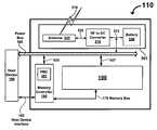
- FIG. 1Adepicts an example of a memory device configured to preserve values representing data, according to various embodiments of the invention.
- memory device 100includes a trigger circuit 120 , a preservation circuit 140 , and a memory 160 .
- Connection 122couples trigger circuit 120 with preservation circuit 140
- connection 162couples preservation circuit 140 with memory 160 .
- memory 160includes multiple layers of memory cells configured to store logic states associated with values, such as resistance values.
- Preservation circuit 140may be coupled with the memory cells, such as via connection 162 . In operation, preservation circuit 140 may be configured to preserve the resistance values that represent particular logic states. In one embodiment, preservation circuit 140 may be configured to preserve one or more resistance values that represent a particular logic state.
- preservation circuit 140may preserve the resistance value of a memory cell so that it falls within a range of resistances that represent a specific logic state, such as logic “1” or a logic “0”, for example.
- Trigger circuit 120may generate and transmit a trigger signal to preservation circuit 140 via connection 120 , which, in turn, performs a preservation operation.
- a preservation operationincludes rewriting data into at least a portion of the memory cells in memory 160 prior to, for example, the expiration of a power absence period.
- a preservation operationmay restore a resistance value for a certain logic state so that the logic state remains substantially unchanged over time during absences of power (i.e., without powering one or more memory elements associated with the resistance value).
- preservation circuit 140in whole or in part—may ensure data retention for memory 160 .
- a memory device 100 that uses preservation circuit 140may enhance the non-volatile nature of memory 160 to extend its data retention to at least that of known non-volatile memory technologies, such as Flash memory, or longer.
- trigger circuit 120may be configured to initiate a preservation operation on any number of memory locations, and, thus, on any number of memory elements for the memory locations. When a preservation operation is performed on each memory location in memory 160 during a power absence period, then the integrity of the data stored therein is ensured, at least until the end of the power absence period. Consequently, when memory device 100 uses preservation circuit 140 and trigger circuit 120 , then data may be retained in memory 160 over multiple power absence periods.
- preservation circuit 140 and trigger circuit 120may operate to retain data in memory 160 for ten (10) years or longer, with other influencing factors remaining unchanged.
- trigger circuit 120may be configured to generate a trigger signal in response to a triggering event.
- the triggering eventmay represent a change (or a sufficient change) in power applied to memory device 100 or any of its constituent elements, such as memory 160 .
- the trigger signalmay be a power-up signal that indicates power has been applied to memory device 100 (or any of its constituent elements), according to one embodiment.
- the triggering eventis a power-up event.
- the trigger signalmay be a power-down signal that indicates the application of power to memory device 100 has ceased.
- trigger circuit 120may be configured to apply a power-down signal to preservation circuit, which, in turn, may perform a preservation operation before power to memory device 100 is sufficiently depleted (e.g., from a battery, capacitor, or other power types of power sources).
- the triggering eventis a power-down event. Note that the triggering event is not limited to representing changes in power and may represent any other type of event affecting the operation of memory device 100 .
- Memory device 100 of FIG. 1Ais shown to be accessible with a memory bus interface 142 .
- a host computing device(not shown) may be coupled with memory device 100 using memory bus interface 142 .
- the structure and/or functionality of preservation circuit 140(or portions thereof) may be omitted, and the host may implement the structure and/or functionality for preservation circuit 140 .
- the host devicemay provide power for performing preservation operations.
- the host computing deviceis absent, whereby an alternate power source (e.g., a battery) may provide the power for performing preservation operations under control of preservation circuit 140 .
- an alternate power sourcee.g., a battery
- trigger circuit 120is opportunistic. That is, when external power is applied to trigger circuit 120 may perform preservation operations in an expeditious manner so as to restore values (e.g., resistive values) for as many memory elements as possible while external power is available. Also, trigger circuit 120 may opportunistically use memory bus interface 142 to perform preservation operations during periods of low bus usage by a host, so as not to interfere (or to negligibly affect) read and write operations invoked by the host. Low bus usage may relate to low usage of memory bus interface 142 during low rates of data access between the host and memory 160 .
- trigger circuit 120may recalibrate the rate at which it initiates preservation operations so as to meter the rate at which the power source, such as a battery, expends power.
- trigger circuit 120may periodically (or aperiodically) send signals (“trigger signals”) via connection 122 to initiate, for example, a rewrite operation on memory 160 as a preservation operation.
- a rewrite operationincludes reading contents of memory 160 and rewriting the contents back to memory 160 , for example, via connection 162 .
- memory device 100may be configured to rewrite its contents at least once before the expiration of each power-absence period, thereby maintaining the contents until the next power-absence period.
- the power-absence periodmay dictate the minimum rate at which to preserve memory contents.
- the longer the power-absence periodthe slower the preservation rate, which, in turn, may reduce the power consumed to perform preservation operations. For instance, if a memory is able to maintain its contents without power for a period of, for example, thirty (30) days, power that otherwise might be used to power memory 160 may be shut off for up to a period of thirty days of inactivity. Power may be selectively turned on when the memory is accessed (e.g., by a host) or when memory contents need to refresh to maintain through the next period of 30 days.
- FIG. 1Ashows trigger circuit 120 coupled via connection 122 to preservation circuit 140 for communicating at least trigger signals
- trigger circuit 120may be communicatively coupled with preservation circuit 140 by other structures (not shown).
- either trigger circuit 120 or preservation circuit 140 , or bothmay be external to memory device 100 (not shown).
- memory bus interface 142may be connected with a memory bus 170 ( FIG. 1C ) or connected with a memory controller 180 (not shown).
- trigger circuit 120may be included in preservation circuit 140 ( FIG. 1C ).
- memory device 100does not include a trigger circuit. Instead, one or more software, middleware, firmware, driver, and the like, may provide functions similar to trigger circuit 120 .
- preservation circuit 140may be configured to communicate with at least one software-based trigger utility, either in place of, or, in addition to, trigger circuit 120 .
- preservation circuit 140may be included in a memory chip ( FIG. 1C ).
- memory device 100does not include a preservation circuit, as described above.
- one or more software utilitiesmay provide functions similar to preservation circuit 140 , but may be implemented in a host device (not shown).
- one or more software trigger utilitiesmay be configured to access memory 160 (e.g., directly) to perform preservation operations.
- memory device 100includes more than one preservation circuits 140 that may interact with one or more memory chips ( FIG. 1C ).
- Memory 160may be formed with one memory chip, or two or more memory chips.
- a memory chipmay be formed with a single layer of memory cells, or with two or more layers of memory cells ( FIG. 1B ).
- FIG. 1Bdepicts a memory device 100 a , according to at least one specific embodiment of the invention.
- Memory device 100 aincludes multiple memory layers 160 a (e.g., layers 161 a , 161 b , 161 c , and 161 d vertically disposed along the Z-axis) and a logic layer 130 .
- Memory device 100 bmay include more of fewer layers than those depicted in FIG. 1B .
- each memory cellmay be a two-terminal element in multiple memory layers 160 a , as described in U.S. patent application Ser. No. 11/095,026, entitled “Memory Using Mixed Valence Conductive Oxides,” which describes one example of a two-terminal memory cell.
- each memory cellmay include a three-terminal element, such as a memory element in a Flash memory device or SRAM memory device.
- Logic layer 130may be electrically coupled with the multiple memory layers 160 a by way of a plurality of vias or ports (not shown) to communicate control signals and data signals. In a specific embodiment, a subset of these ports may form one or more connections to preservation circuit 140 (e.g., of FIG. 1B ) and/or memory bus 170 (e.g., of FIG. 1C ). In the example shown, logic layer 130 may include trigger circuit 120 , preservation circuit 140 , and memory controller 180 of FIG. 1B . In some implementations, logic layer 130 does not include either trigger circuit 120 or preservation circuit 140 , or both.
- the logic layer 130may be fabricated on a substrate 151 (e.g., a silicon substrate) and may comprise CMOS circuitry for implementing the circuits 120 , 140 , and 180 , and other circuitry, for example.
- the multiple memory layers 160 amay be fabricated over the logic layer 130 (e.g., along the Z-axis) with the layers 161 a , 161 b , 161 c , and 161 d vertically stacked over the substrate 151 and electrically coupled with circuitry in the logic layer 130 using an interconnect structure (not shown), such as vias and the like, for example.
- the configuration depicted in FIG. 1Bmay also be implemented for a single layer of memory (e.g., the memory 160 ) fabricated over the substrate 151 with the single layer of memory in electrical communication with circuitry in the logic layer 130 .
- Each layer of memorymay include a non-volatile two-terminal cross-point memory array 165 .
- the array 165includes a plurality of first conductive traces 167 (e.g., row conductors) and a plurality of second conductive traces 168 (e.g., column conductors).
- the plurality of first conductive traces 167do not come into direct contact with one another and the plurality of second conductive traces 168 do not come into direct contact with one another or into direct contact with any of the plurality of first conductive traces 167 .
- the array 165includes a plurality of two-terminal memory elements 166 with each memory element positioned at an intersection of one of the first conductive traces with one of the second conductive traces (i.e., is positioned at a cross-point).
- a first terminal (not shown) of each memory element 166is electrically coupled with only one of the plurality of first conductive traces 167 and a second terminal (not shown) of each memory element 166 is electrically coupled with only one of the plurality of second conductive traces 168 .
- Each terminalmay include one or more layers of electrically conductive materials and those materials may include glue layers, adhesion layers, anti-reflection layers, anti-diffusion layers, and the like.
- platinumPt
- Each memory element 166is configured to store data as a plurality of conductivity profiles that can be non-destructively determined by applying a read voltage across the first and second conductive traces ( 167 , 168 ) that are electrically coupled with the first and second terminals of the memory element 166 .
- Data operations to the array 165are effectuated by applying the appropriate magnitude and polarity of a select voltage across the first and second conductive traces ( 167 , 168 ) of one or more selected memory elements 166 .
- the magnitude of a read voltageis less than the magnitude of a write voltage so that stored data is not corrupted by the application of the read voltage (i.e., the conductivity profile is not changed by application of the read voltage).
- the read voltagemay have a magnitude of about 3V or less and a write voltage may have a magnitude of about 4V or greater.
- Circuitry in the logic layer 130is electrically coupled (e.g., using vias or the like) with the first and second conductive traces ( 167 , 168 ) of each array 165 and is operative in part, to apply the select voltages to selected memory elements 166 and to sense read currents flowing through the selected memory element 166 , for example. Moreover, the circuitry in the logic layer 130 may effectuate data operations to the memory elements 166 in one or more of the arrays 165 using page mode data operations or burst mode data operations.
- memory controller 180may perform memory control functions similarly performed by known memory devices, such as a USB memory storage device, a Flash memory card, a DRAM memory device, a SRAM memory device, or the like. For example, when host device 190 (discussed below) transmits write data to memory device 100 a , memory controller 180 may apply the appropriate control signals and data to memory 160 a to select one or more memory cells for storage. Similarly, in serving a read request by host device 190 , memory controller 180 may be configured to locate the address or addresses for the memory cells that hold the requested data, and may retrieve the stored data to host device 190 . Memory controller 180 may control access to multiple memory layers 160 a via, for example, memory bus 170 of FIG.
- Memory bus 170 of FIG. 1Cmay be formed with a subset of ports (not shown) in the logic layer 130 and multiple memory layers 160 a .
- trigger circuit 120 and preservation circuit 140may be formed in one or two integrated circuit (“IC”) chips separately from the chip that contains memory controller 180 .
- Memory controller 180may include a memory bus (not shown) or a host device interface 182 ( FIG. 5 ) that interacts with a memory-using host device 190 ( FIG. 5 ).
- a memory-using host device 190may be configured to embed and/or attach more than one memory devices 100 and/or 110 ( FIG. 5 ).
- FIG. 1Cdepicts a variety of possible configurations for an exemplary memory device 100 b , according to various embodiments of the invention.
- Memory 160may be configured with any number of memory chips.
- memory 160may be formed with one, two, four, or more memory chips.
- FIG. 1Cshows at least four memory chips 160 a , 160 b , 160 c , and 160 d .
- Each memory chipmay include either a single layer of memory cells or a plurality of layers of memory cells.
- chips 160 a and 160 ceach may include at least two layers of memory cells.
- chips 160 b and 160 dare depicted as single-layered memory.
- connections 162 a to 162 dthere may be two or more connections 162 a to 162 d from memory 160 .
- one or more connections 162 a to 162 dmay be configured to connect to one or more preservation circuits (“PC”) 140 , 140 a , 140 b , and 140 c .
- PCpreservation circuits
- one or more connections 162 a to 162 dmay interface with memory bus 170 .
- at least one of connections 162 a to 162 dinterfaces with preservation circuit 140
- at least one other of connections 162 a to 162 dinterfaces with memory bus 170 .
- memory 160may be configured to communicate with memory bus 170 directly.
- memory device 100 bmay include more than one trigger circuit 120 that may communicate with one or more preservation circuit (“PC”) 140 , 140 a , 140 b , and 140 c . As shown, memory device 100 b may be coupled with host device 190 . Memory device 100 b may be coupled with, attached to, connected to, or embedded in host device 190 in various ways. For example, memory device 100 b may be plugged into a memory slot or port of host device 190 or irremovably fixed to host device 190 .
- PCpreservation circuit
- the memory slot or portmay be adapted to communicate using any protocol, for example, a protocol used in known ports or slots, such as USB, PCMCIA, CompactFlash®, Secure Digital (SDTM), Micro SDTM, SD High Capacity (SDHCTM), Memory StickTM, and xD-PictureTM.
- a protocol used in known ports or slotssuch as USB, PCMCIA, CompactFlash®, Secure Digital (SDTM), Micro SDTM, SD High Capacity (SDHCTM), Memory StickTM, and xD-PictureTM.
- Host device 190may be any device that is capable of using a memory device, such as any host described herein.
- a hostmay be a computing device, such as a hand-held computer, laptop, desktop, or mainframe system; an electronic device, such as a disk drive, network access storage, network or wireless access point, network router, or network gateway; a consumer electronic device, such as a personal digital assistant (PDA), smart phone, cellular phone, general purpose phone, camera, video recording device, television, radio, audio system, MP3 player, or game console.
- PDApersonal digital assistant
- host device 190may be adapted for use in a vehicle, such as an automobile, boat, ship, airplane, train, and the like.
- Host device 190may include at least a processor and at least one input/output (I/O) sub-device, such as an input key, switch, mouse, touch screen, infrared transceiver, wireless interface (e.g., RF), or communication bus.
- Host device 190may include a display, screen, or printing sub-device, as well as data storage, such as SRAM, DRAM, or another memory devices. In some embodiments the data storage of host device 190 may be used to temporarily store data that is rewritten back into memory 160 for preservation purposes.
- a memory chip in memory device 100 bmay be formed so as to include a preservation circuit.
- chips 160 b , 160 c , and 160 dare each shown to contain a preservation circuits (“PC”), 140 a , 140 b , and 140 c , respectively.
- the preservation circuitsmay be positioned in the logic layers 130 of their respective memory chip.
- a preservation circuit inside a chipmay perform preservation operations, such as rewrite operations, by sending rewrite instructions to the memory in the corresponding chip.
- a preservation circuit inside a chipsuch as PC 140 c , may be configured to send rewrite instructions to other part of memory 160 , for example, to another chip, such as chip 160 a .
- a memory chip in memory device 100 bmay be formed so as to include a trigger circuit.
- chip 160 dmay be formed to include a trigger circuit (“TC”) 120 a .
- a trigger circuit inside a chipmay provide trigger signals to a corresponding preservation circuit inside that chip.
- the trigger circuit 120may be positioned in the logic layers 130 of their respective memory chips.
- a trigger circuit inside a chipsuch as trigger circuit 120 a , may be configured to provide trigger signals to one or more preservation circuits outside that chip, such as any of preservation circuits 140 , 140 a , and 140 b .
- memory device 100 bdoes not include trigger circuit 120 or preservation circuit 140 , or both.
- the functionalities of trigger circuit 120 and preservation circuit 140may be provided by one or more entities (not shown), such as host device 190 , which may be external to memory device 100 b .
- the external entitymay use hardware, software, or both to implement an equivalent functionality of the trigger and preservation circuits.
- trigger circuit 120 of FIG. 1Cmay interface via a memory bus interface 242 with one or more preservation circuits 140 , 140 a , and 140 b .
- preservation circuit 140may send rewrite instructions or commands via memory bus interface 242 to memory 160 or part of memory 160 .
- one or more memory chipsinclude separate preservation circuits, such as the memory chips 160 b , 160 c , and 160 d
- the respective memories in the chipsmay be rewritten by the associated preservation circuits 140 a , 140 b , and 140 c .
- Two or more trigger circuits, for example 120 and 120 amay be configured to issue trigger signals at different rates due to different memories having different power absence periods.
- trigger circuit 120may be configured to send one trigger signal every 10 seconds while trigger circuit (“TC”) 120 a may be configured to send one trigger signal every 12 hours.
- two or more preservation circuitsfor example, 140 , 140 a , 140 b and 140 c , may be configured to institute different preservation or restoration schemes, when two preservation circuits, such as, 140 a and 140 b , are responding to the same trigger circuit or trigger signals that are implemented at the same rate.
- different portions of memory 160such as different chips, may be rewritten or restored by different methods, independent of other portions.
- memory 160may be rewritten by a single process.
- a portion of memory 160is configured to be rewritten or restored by a software utility.
- a portion of memory 160may be configured to so as not to be rewritten or restored.
- FIG. 2Adepicts a trigger circuit 120 , according to one or more embodiments of the invention.
- Trigger circuit 120may include a clock 230 and a timer 240 , as well as one or both of preservation circuit interface 122 and memory bus interface 242 , which is configured to communicate signals, such as trigger signals, reset signals, power-on signals, power-off signals, etc.
- Clock 230may be configured with any of the known clock sources, such as resistor-capacitor (“RC”) oscillators, silicon oscillators, crystals oscillators, and ceramic resonators, for example.
- clock 230may be configured with a RC oscillator or circuit.
- clock 230is a real-time clock.
- a real-time clockmay include a circuit that utilizes an accurate clock source to generate time signals representative of units of time, such as seconds, minutes, and hours.
- a real-time clockmay be configured to generate time signals representative of units of time, such as days, weeks, and/or months.
- Clock 230also may be configured with a clock source that oscillates at any frequency.
- the desired time signals of clock 230may be slower than the frequency of a clock source, such as a real-time clock source.
- the output of the clock sourcemay be attached to a counter or a ripple counter (discussed below) to slow down the frequency of the clock source to generate the desired time signals.
- timer 240may be connected with a real-time clock, and may configured to generate a trigger signal at least once per “wake-up” period, which may be in any unit of time, such as milliseconds. Timer 240 may operate by counting to (i.e., reaching) a wake-up time, which triggers or causes timer 240 to send a trigger signal.
- the wake-up timemay be referred to as a triggering event, according to one embodiment.
- a wake-up timemay be set at manufacturing, by programming, by software, or by a switch (not shown).
- a switchmay be a mechanical switch, such as a jumper port, toggle button, or pin-size contact button, or other mechanical selection devices.
- a switchmay also be an electronic switch, such as a transistor, a relay, a pass gate, a register storing one or more data bits, or the like.
- a switchmay have one or more positions, each representing a different wake-up time setting. Wake-up time settings for one or more switch positions may be modified by programming, by software, or by other manipulations.
- a switchmay have one or more positions that are shared with, or used by other, components or circuits, such as preservation circuit 140 , of a memory device.
- timer 240may be configured to receive the wake-up time from a host device (not shown) so as to be able to modify the rate of rewriting the memory, based on the host device application, the length of time that external power is available, and the like.
- timer 240may be coupled 251 with clock 230 and be driven by clock pulses generated by the clock 230 .
- timer 240may be set to generate a trigger at a specific wake-up time of, for example, 500 milliseconds (ms). So, for each clock pulse, clock 230 may cause the timer 240 to advance by one count. In some embodiments, clock 230 may cause the timer 240 to advance by one count for each N number of clock pulses, where N>1.
- timer 240When timer 240 counts to the set wake-up time, which may be a triggering event, timer 240 sends a trigger signal through one or both preservation circuit interface 122 and memory bus interface 242 (e.g., via 253 and/or 255 ), depending on, for example, the source of power with which to perform preservation operations. Timer 240 then may reset itself, and start counting from zero time.
- a power sourcee.g., a battery
- timer 240may be configured with a ripple counter or a ripple timer.
- the triggering eventmay be configured to occur when the ripple counter reaches all ones (“11111111”) or all zeros (“00000000”).
- a trigger signalmay be sent when the ripple counter counts to zero or when it is reset, for example, by an external reset signal (e.g., coupled with the timer 240 via bus interface 242 ).
- a ripple countermay be coupled with a RC clock, in some embodiments. For example, consider that a RC clock, with a clock period of 200 ms (one clock pulse every 200 ms), may be coupled with a ten-bit ripple counter. Thus, trigger circuit 120 may reach a triggering event after every 2,048,000 ms (200 ms ⁇ 2 10 ) or 204.8 seconds.
- timer 240may be reset by an event external to trigger circuit 120 .
- a power-on (or power-up) event or a power-off (or power-down) eventmay cause timer 240 to reset.
- trigger circuit 120(of any of FIGS. 1A to 1C ) may be configured with a switch that, when activated, sends a reset signal to timer 240 .
- the terms “power on” and “power up”refer, in at least one embodiment, to a condition when electric power starts flowing into a system; into a device, such as a host device or a memory device; or into a component, such as any of the following: trigger circuit 120 , preservation circuit 140 , memory 160 , memory bus 170 , memory bus interface 242 , and/or memory controller 180 .
- a “power on” or “power up” eventmay occur under numerous situations, including establishing connectivity to a power source; or when any system, device, or component starts supplying power for any reason to memory device 100 , or the like; or when detecting reception of radio frequency (“RF”) signals used to generate power for storage in a power source.
- RFradio frequency
- the host devicemay supply power to the memory device, which is a power-up (or power on) event.
- a power-up eventmay occur when the host is powering-on (or awakening) from a stand-by mode or hibernation mode.
- the detection of RF signalswhich are for power conversion purposes described below, may be considered a power up event.
- the terms “power off” and “power down”may refer, in at least one embodiment, to electric power that stops flowing (or is sufficiently curtailed) into a system, a device, or a component.
- a “power off” or “power down” eventmay occur under numerous situations, such as disconnecting from a power source; and interrupting the supply of power, for any reason, by another system, device, or component.
- trigger circuit 120is configured to detect a power down event, and to generate a power-down trigger signal, which, in turn, causes at least one preservation circuit to perform a preservation operation before power to the memory device is sufficiently depleted.
- the sensing of a power-on event and a power-off event by either at least one trigger circuit or at least one preservation circuitmay generate a power-on signal and a power-off signal, respectively.
- a wake-up timemay be modified, for example, by a software utility, by programming trigger circuit 120 , or by changing a switch to a different position.
- setting a new wake-up timeis a triggering event, which may cause timer 240 to generate a trigger signal.
- timer 240may reset to zero, and then start counting to the new wake-up time.
- Timer 240may be set to any wake-up time from 100 milliseconds to 90 days, or longer. For example, timer 240 may be set to 100 ms, 204 ms, 267 ms, 300 ms, 731 ms, 1021 ms, etc.
- timer 240may be set in units of tenths of seconds or seconds (“s”), such as 0.3 s, 0.8 s, 35 s, 100 s, and so on. In other implementations, timer 240 may be set in units of minutes (“m”), hours (“h”), and days (“d”), such as 1 m, 15 m, 1 h, 6 h, 1 d, 2 d, 10 d, 30 d, 90 d, or longer. For example, one skilled in the art can readily build a timer that accepts the setting of wake-up time in any combination of units, such as 2 d 3 h 25 m 42 s or an equivalent thereof.
- trigger signalsare substantially regular and periodic, with substantially uniform intervals between trigger signals. For example, if wake-up time is set at 400 ms, trigger signals may be transmitted every 400 ms (e.g., about 400 ms in between trigger signals). In other embodiments, trigger signals are aperiodic, whereby trigger signals are not separated by substantially the same time period in between. For example, a current trigger signal may come 400 ms (the wake-up time) after a pervious trigger signal, with a subsequent trigger signal coming 917 ms after the current trigger signal. In this example, the time deviates from the wake-up time of 400 ms by as much as 517 ms (917 ms ⁇ 400 ms).
- the deviation timemay be selected by, for example, a switch, hardware, programming, and/or software. For example, if trigger circuit 120 is set a trigger time of 10 seconds and a deviation time of five seconds, trigger circuit 120 may issue trigger signals separated by a period of about five to 15 seconds. In some embodiments, the deviation time may be expressed in percentage, such as wake-up time plus or minus up to ⁇ 50%. Regardless, trigger circuit 120 may opportunistically issue trigger signals aperiodically as a function of, for example, the bandwidth of a path between a host accessing the memory, whereby trigger circuit 120 issues more trigger signals when there is lower bus usage between a host and the memory, and issues fewer trigger signals when there is higher bus usage.
- trigger circuit 120may opportunistically issue trigger signals aperiodically as a function of, for example, the voltage of a power source (e.g., a battery), whereby trigger circuit 120 may issue more trigger signals per interval of time when there is more charge stored in the power source than when there is less.
- the power sourcemay be a battery (e.g., a rechargeable battery), a capacitor, or any other mechanism for storing electrical charge.
- a suitable power sourcemay include a Micro-Electro-Mechanical System (“MEMs”) flywheel, or the like.
- FIG. 2Bdepicts an exemplary a preservation circuit configured to include a rewrite processor, according to at least one embodiment of the invention.
- Preservation circuit 140includes a rewrite processor 260 .
- preservation circuit 140includes one or more nonvolatile registers 270 to maintain memory content information.
- preservation circuit 140includes one or more buffers 280 .
- buffer 280may be sized to hold one or more bits of data. A small buffer may be implemented with a single bit register in a specific embodiment.
- preservation circuit 140includes trigger circuit 120 as shown in FIG. 1C .
- Preservation circuit 140may include at least one signaling interface 222 for communicating signals, such as reset signals, power on signals, power off signals, and trigger signals. Trigger signals may come from one or more software utilities, or from a trigger circuit 120 . In the latter case, signaling interface 222 may be coupled with preservation circuit interface 122 of trigger circuit 120 to communicate trigger signals. Preservation circuit 140 may also include one or both of memory bus interface 142 and memory interface 262 for communicating control signals and data signals.
- preservation circuit 140may operate to perform reading, writing, and rewriting of memory contents. Examples of reading and writing or storing, in the context of memory access, are described in U.S. patent application Ser. No. 11/095,026, entitled “Memory Using Mixed Valence Conductive Oxides,” which involves one example of a resistive-based memory.
- the term “rewriting” or “restoring” in the context of a modifying the contents of memoryin at least one embodiment, refers to writing to a memory with data read from that memory, either from the same location or a different location.
- each two-terminal memory elementmay store a single bit of data as one of two distinct conductivity profiles with a first resistive state R 0 at a read voltage V R indicative of a logic “0” and a second resistive state R 1 at V R indicative of a logic “1”, where R 0 ⁇ R 1 .
- a change in conductivity, measured at V R , between R 0 and R 1differs by at least a factor of approximately 10 (e.g., R 0 ⁇ 1 M ⁇ and R 1 ⁇ 100 k ⁇ ).
- the memory elementsare not necessarily linear resistors and the resistance of the memory elements may not be a linear function of the voltage applied across the memory elements. Therefore, a resistance R of the memory elements may approximately be a function of the read voltage V R such that R ⁇ f (V R ).
- the R 0 and R 1may be retained in the absence of power (e.g., no applied voltage across the two terminals of the memory element) and the application of the read voltage may be non-destructive to the values of R 0 and R 1 .
- the values of R 0 and R 1may drift over time due to several factors including but not limited to successive read operations to the same memory element and changes in conductivity of the memory element over time.
- one memory elementstores a logic “0” (e.g., R 0 ⁇ 1 M ⁇ ) and another memory element stores a logic “1” (e.g., R 1 ⁇ 100 k ⁇ )
- those values of resistancemay drift over time (e.g., after 18 months) such that after a period of time R 0 may decrease from about 1 M ⁇ to about 600 k ⁇ and R 1 may increase from about 100 k ⁇ to about 350 k ⁇ .
- the read voltage V Ris applied across the two terminals of the two-terminal memory element, a read current I R flows through the memory element and a magnitude of the read current I R is indicative of the value of data stored in the memory element.
- the magnitude of the read current I R for the R 0 resistive stateis lower than the magnitude of the read current I R for the R 1 resistive state.
- Sense circuitrye.g., in the logic layer 130 operative to sense the magnitude of the read current I R and convert the value sensed into a logic voltage level may not be able distinguish between the read currents indicative of the R 0 and R 1 resistive states if the resistive values for R 0 and R 1 have drifted as described above. Essentially, unacceptably large amounts of drift in resistive values may result in data corruption. Drift may occur do to several factors including but not limited to the passage of time since the last write operation to a memory element and successive read operations to a memory element. Accordingly, the process of restoring or rewriting is operative to restore the resistive value of R 0 from about 600 k ⁇ to about 1 M ⁇ and to restore the resistive value of R 1 from about 350 k ⁇ to about 100 k ⁇ .
- the process of restoring or rewritingmay include applying an appropriate magnitude of a write voltage V W across the two terminals of the two-terminal memory element to effectuate writing the R 0 or R 1 resistive value to a memory element selected for a restore operation.
- a first magnitude and polarity of a write voltage V W0may be used to effectuate a restore operation on a memory element that stores the R 0 resistive value
- a second magnitude and polarity of a write voltage V W1may be used to effectuate a restore operation on a memory element that stores the R 1 resistive value.
- the resistive value of a memory element storing the R 0 resistive valuewill have increased from about 600 k ⁇ to about 1 M ⁇ , for example.
- the resistive value of a memory element storing the R 1 resistive valuewill have decreased from about 350 k ⁇ to about 100 k ⁇ , for example.
- Preservation circuit 140may be configured to respond to a trigger signal by performing a rewrite operation to a memory (or a portion thereof) in a memory device.
- preservation circuit 140may read a portion of memory, write the contents from the portion of memory to buffer 280 , read the data in buffer 280 , and then rewrite the contents back into the memory.
- the portion of memoryis rewritten to the same location from which it was read. In other embodiments, the portion of memory is rewritten to a different location.
- preservation circuit 140is configured without a buffer 280 , whereby preservation circuit 140 may perform the rewrite operation by reading a portion of memory from a first location and rewriting the portion of memory to a second location of the memory. In one or more embodiments, preservation circuit 140 is configured to read into its buffer 280 part of a portion of memory, read the remaining of the portion of memory, rewrite the remaining of the portion into the memory, then rewrite the contents of buffer 280 into the memory.
- Preservation circuit 140may be configured to perform a rewrite or restore operation according to one or many schemes. A different scheme or process may be programmed into preservation circuit 140 . In some embodiments, preservation circuit 140 may be configured with a switch (not shown), such as one discussed above, to select different pre-defined rewrite schemes.
- One having ordinary skill in the artcan practice various embodiments of the invention with other methods or schemes, including one or more schemes derived from those described herein.
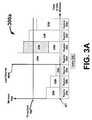
- FIG. 3Adepicts an example of a method 300 a that uses two or more registers, according to one or more embodiments of the invention.
- Registers 320 a to 320 gmay be nonvolatile or volatile, depending on application specific requirements.
- the x-axisshows the total in-use memory.
- in-use memoryrefers, in at least one embodiment, to the portion or portions of memory that is used to store data, regardless of where the data is residing in the memory.
- the total in-use memoryis 200 MB.
- the in-use memorymay be in one or more locations of the memory or scattered across the memory.
- the y-axisshows the memory age of different portions of the in-use memory.
- the term “memory age”refers, in at least one embodiment, to the time period between current time and the time a portion of memory was last written, rewritten or restored for purposes of preservation (e.g., during a power absence period for data retention purposes).
- portion 310 awas last restored 155 seconds ago, the memory age of portion 310 a is 155 seconds.
- the total in-use memoryis roughly divided into seven portions 310 a to 310 g .
- seven registers 320 a to 320 gare used to maintain information about the memory contents of the seven portions 310 a to 310 g of memory.
- Index 330which may be another register, volatile or nonvolatile, may be configured to record which was the last portion of memory rewritten.
- preservation circuit 140In operation, described from an origin 301 of the x-y plane of scheme 300 a , preservation circuit 140 sits idle, awaiting a trigger signal. Index 330 , at this point of operation, points to the last portion of memory rewritten 310 g , which is the portion, viewed in a loop, before portion 310 a .
- preservation circuit 140detects a trigger signal, it sends a wait signal or a halt signal to lockup memory bus 170 of FIG. 1C for a rewrite operation.
- a wait signalmay be sent when a relatively small portion of the memory is to be rewritten. For example, a few bytes or a few kilobytes.
- the wait signalsstalls access by a host device until a preservation operation expires (i.e., after the few bytes or a few kilobytes are preserved or rewritten). For a larger portion, a halt signal may be sent.
- Preservation circuit 140then may send control signals to read the portion of memory after the portion pointed to by index 330 .
- the portion to be readis portion 310 a .
- Preservation circuit 140reads portion 310 a into its buffer and rewrites or restores portion 310 a to the memory, either to the location portion 310 a was read from or to a new location.
- Preservation circuit 140then may send a signal to unlock memory bus 170 , and updates register 320 a with a timestamp that marks the current moment.
- a timestampmay include a date and time down to the milliseconds, for example.
- preservation circuit 140may update index 330 to point to portion 310 a as the last portion rewritten. Index 330 holds the logical pointer that marks the last time a rewrite operation was performed (last rewrite mark in FIG. 3A ). Preservation circuit 140 then goes into idle mode until another trigger signal causes another rewrite operation.
- Preservation circuit 140may be configured to ignore one or more trigger signals. If a trigger signal is not ignored, preservation circuit 140 performs rewrite operation to the next portion 310 b of in-use memory. A trigger signal then triggers preservation circuit 140 to rewrite portion 310 c of the in-use memory. At this time, index 330 advances to point to portion 310 c and the last rewrite mark advances to a position shown FIG. 3A . Note that the next portion of memory to be rewritten, portion 310 d , immediate to the right of the last rewrite mark, has the oldest memory age. The portion just rewritten, 310 c , immediate to the left of the last rewrite mark, has the youngest memory.
- a threshold agemay be used, the threshold age indicating to preservation circuit 140 which portions to rewrite, in response to the next trigger signal.
- all portions of memory with age older than the threshold agemay be subject to a preservation operation. As shown, three portions 310 d , 310 e , and 310 f have memory older than the set threshold age.
- preservation circuit 140may operate to rewrite all three portions 310 d , 310 e , and 310 f .
- the age of a portion of memorymay be updated by other components of a memory device, such as memory controller 180 .
- preservation circuit 140may increase the performance of its rewrite operation by skipping portion 310 e ′ when it rewrites memory portions older than the threshold age. The last rewrite mark then advances to after portion 310 f , last portion rewritten. The next rewrite operation will be performed on portion 310 g . Preservation circuit 140 then loops back to the origin 301 of the x-y plane, goes idle, and waits for the next trigger signal.
- the threshold ageis set according to the power-absence period of a memory. For example, if a memory may maintain its contents for a period of 90 days in the absence of power, the threshold age may be set to at most 90 days. The threshold age is likely to be set at 90 days minus a grace period, such as 90 days minus 15 days, or 75 days. The grace period may be selected according to the natures of an application, condition, or situation the memory will likely to be used in. For example, if a memory with a 90-day power-absence period is likely to be unplugged from a host device for up to 60 days at a time, a likely grace period is 60 days or more. Threshold age for this particular application should be 90 days minus at least 60 days equal at most 30 days. Thus, in this example, no memory portion will be older than 30 days, and the memory may maintain its contents for another 60 days in the absence of power.
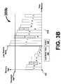
- FIG. 3Bdepicts an alternative exemplary method 300 b , according to one or more embodiments of the invention.
- This methoddiffers from method 300 a in three places: (1) the x-axis of method 300 b shows total memory, (2) method 300 b divides the memory into more portions, of which 21 portions 310 a to 310 u are shown, and (3) method 300 b uses one register, last write time 322 , to record the completion timestamp of the rewrite operation to every portion.
- method 300 bfavors applications that frequently use close to the maximum capacity, 4 GB for example, of the memory.
- Preservation circuit 140in accordance with method 300 b , may perform substantially the same operation as in method 300 a , except in relation to two features. At the completion of a rewrite operation on any portions 310 a to 310 u , preservation circuit 140 writes the current timestamp into last write time register 322 . Before a rewrite operation, preservation circuit 140 determines how many portions to rewrite with two timestamps: the current timestamp and the timestamp recorded in last write time 322 .
- preservation circuit 140In a first example, if preservation circuit 140 is configured to rewrite the entire memory in 21 days and current time is five days after the time recorded in last write time 322 , preservation circuit 140 will rewrite five portions 310 j to 310 n after the portion 310 i pointed to by index 330 . In a second example, if preservation circuit 140 is configured to rewrite the entire memory in 42 hours and current time is four hours after the time recorded in last write time 322 , preservation circuit 140 will rewrite two portions 310 j and 310 k after the portion 310 i pointed to by index 330 . If method 300 b also implements memory threshold age in the second example, two additional portions 310 l and 310 m will be included in the rewrite operation that is described above.
- method 300 bmay be implemented with one or more registers (not shown) to record the rewrite time of each memory portion, as in method 300 a .
- memory age of memory portionssuch as 310 c ′, 310 m ′, and 310 p ′, may be updated by other components of the memory device, such as the memory controller 180 , when the contents of these memory portions are modified or written. As such, a memory portion with an age below the threshold age will not be included in the next rewrite operation.
- preservation circuit 140may be configured to rewrite all memory in response to a trigger signal.
- preservation circuit 140is coupled with a switch, such as one described above, to provide an additional input to preservation circuit 140 in its determination of what portions of memory to rewrite.
- a switchmay be configured to include two or more positions, and the meanings of the positions may be changed.
- a switchmay be configured with four positions—p1, p2, p3, and p4—that indicate to preservation circuit 140 to rewrite 25%, 50%, 75%, and 100% of the memory, respectively.
- the meanings of these positions (p1, p2, p3, and p4)may be reprogrammed, or otherwise changed, to indicate to preservation circuit 140 , for example, to rewrite: (p1) 100% on a power-on event, (p2) 0% on power-on event, (p3) follow a predetermined scheme, for example, as described in FIG. 3A or 3 B, and (p4) 100% when memory is not being access by memory controller 180 in, for example, 30 minutes.
- preservation circuit 140may be configured to follow multiple preservation schemes, depending on different trigger signals. For example, a power-on signal or power-off signal will trigger rewriting of the entire memory; a trigger signal from trigger circuit 120 will trigger rewriting of a portion or portions of the memory, as illustrated in FIG. 3A or 3 B; and a reset signal will trigger no rewrite operation other than resetting the registers in preservation circuit 140 to pre-defined states.
- FIG. 4is a flow diagram 400 depicting an exemplary method for rewriting or restoring memory, according to at least one embodiment of the invention.
- a methodperforms a subset of flow diagram 400 and may perform one or more functions, each of which is not shown in FIG. 4 to avoid unnecessarily obscuring the description.
- flow diagram 400 and its constituent elementsmay be performed by one or more of the following: a software utility, a memory device, a trigger circuit, a preservation circuit, a memory controller, or any device implementing or mimicking a memory device, such as an electronic device or a computer program executing instructions to manage information or a database.
- Flow diagram 400shows that a memory may sleep (e.g., placed into a state of low or no power consumption) during a stage 410 .
- stage 410may be skipped at the initial start (but not after a stage 460 , in some cases).
- flow diagram 400waits, delays, sleeps, idles, or otherwise stays inaction for a period of time (“delay period”).
- the delay periodmay be any length of time from 100 milliseconds to days, for example, 90 days, and longer.
- the delay periodmay be changed anywhere (not shown) in flow diagram 400 .
- the passing, expiring or lapsing of the delay periodis a triggering event that may cause flow diagram 400 to advance to a stage 420 .
- a trigger signalis generated, created, issued, sent, or otherwise broadcasted to one or more components, devices, systems, and entities that are configured to receive the trigger signal.
- a receiver of the trigger circuitis preservation circuit 140 .
- a software utilityreceives the trigger signal.
- the trigger circuitmay be generated by the receiving software utility itself, trigger circuit 120 , another software utility, or another device or component. There may be more than one receiver, for example, preservation circuits 140 , 140 a , and 140 b in FIG. 1C may all receive the trigger signal.
- the receiver or receivers of the trigger signalmay determine the amount of memory to rewrite. Determining the amount of memory to rewrite may follow one or more methods described above, a method modified from those described above, or a new method. Determining the amount of memory includes determining the starting point, i.e., the starting memory address, of the amount of memory. When the amount is computed, a rewrite operation begins at a stage 440 . To rewrite the amount of memory, a portion is read from the memory from the starting memory address. The memory may be read into a buffer.
- a software utilityis performing the rewrite operation
- a part of the allocated memory of the system, on which the software utility is executedmay be used as a buffer.
- a preservation circuitis performing the rewrite operation, it may be configured with a buffer to hold the portion of memory.
- the portion of memoryis read from the buffer and written or rewritten back to the memory at the same starting memory address or a different starting memory address.
- a bufferis not used, and the portion of memory is read from a first location of the memory and written or rewritten into a second location of the memory.
- an amount of memory that has been rewrittenis determined. If rewriting is not done, the flow goes back to reading at the stage 440 and rewrites at the stage 450 , to read and rewrite the next portion of the memory, and keeps on reading and rewriting until the amount of memory has been rewritten, at which point, the flow returns to the stage 410 .
- Flow diagram 400continues until it is terminated, or for example, power to a preservation circuit that carries out the processes is lost. Flow diagram 400 may terminate when a software utility that executes instructions carrying out the flow diagram 400 is stopped.
- a computer-implemented or computer-executable version of the flow diagram 400 or part of the flow diagram 400may be embodied using, stored on, or associated with computer-readable medium.
- a computer-readable mediummay include hard disks and any medium that participates in providing instructions to one or more processors for execution. Such a medium may take many forms including, but not limited to, nonvolatile, volatile, and transmission media.
- Nonvolatile mediaincludes, for example, Flash memory, optical disks, or magnetic disks or tapes.
- Volatile mediaincludes static or dynamic memory, such as SRAM or DRAM.
- Transmission mediaincludes coaxial cables, copper wire, fiber optic lines, and wires arranged in a bus. Transmission media may also take the form of electromagnetic, radio frequency, acoustic, or light waves, such as those generated during radio wave and infrared data communications.
- a binary, machine-executable version, of the software of the present inventionmay be stored or reside in DRAM, Flash memory, or on a mass storage device (e.g., hard disk, magnetic disk, tape, or CD-ROM).
- the source code of the software of the present inventionmay also be stored or reside on mass storage device.
- code of various embodiments of the inventionmay be transmitted via wires, radio waves, or through a network such as the Internet or a local area network.
- Computer software productsmay be written in any of various suitable programming languages, such as Java, JavaScript, Perl, C, C++, C#, or Visual Basic, for example.
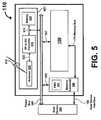
- FIG. 5depicts an example of a memory device 110 including an on-board power supply 501 , according to one or more embodiments of the invention.
- Power supply 501includes an RF-to-DC converter 510 coupled 512 with a battery 530 , both of which may be connected 512 with a power bus 540 .
- power supply 501may include an antenna 520 connected 522 with RF-to-DC converter 510 .
- Memory device 110includes an internal memory device 100 .
- Internal memory device 100may be, for example, any memory device comprising a memory, a trigger circuit, and a preservation circuit, such as depicted in either FIG. 1A , 1 B, or 1 C.
- the memory, trigger circuit, and preservation circuitmay be formed in one IC chip or multiple chips.
- memory controller 180is located inside internal memory device 100 ( FIG. 1B ).
- memory device 110includes memory controller 180 outside internal memory device 100 .
- Memory controller 180connects, attaches, or otherwise couples host device 190 via host device interface 182 to internal memory device 100 via memory bus 170 .
- power bus 540is connected with host device 190 , which supplies power to memory device 110 .
- Power bus 540is configured to supply power to memory controller 180 and internal memory device 100 . Electrical power may flow from host device 190 , RF-to-DC converter 510 , and/or battery 530 .
- RF-to-DC converter 510receives RF signals 518 in a range of frequencies, for example, from 800 to 1000 megahertz, through antenna 520 or through an antenna (not shown) on host device 190 .
- RF-to-DC converter 510is configured to convert RF signals 518 into, for example, direct current (“DC”) power.
- DCdirect current
- RF-to-DC converter 510may be implemented with a Powercast® circuit, designed by Powercast, LLC, of Ligonier, Pa., USA.
- the Powercast) circuitmay be further configured to receive RF signals 518 from a nearby RF signal transmitter.
- RF-to-DC converter 510when RF-to-DC converter 510 is placed within 10 feet of the nearby transmitter, RF-to-DC converter 510 receives RF signals 518 from the transmitter and converts the signals into electricity. The power may be stored in battery 530 . RF-to DC-converter 510 may also directly power trigger circuit 120 , preservation circuit 140 , and memory 160 for internal memory device 100 ( FIGS. 1A to 1C ) in rewrite operations. In some embodiments, RF-to-DC converter 510 receives RF signals 518 from sources typically found in an operating environment, and, thus, does not require a transmitter to provide a source of RF signals 518 .
- Battery 530is configured to store electricity for use in rewrite operations.
- memory device 110includes a power management circuit 181 .
- power management circuit 181may be formed within, memory controller 180 .
- Power management circuit 181may operate to manage power storage and usage in memory device 110 . For example, when memory device 110 is embedded or attached to host device 190 , power management circuit 181 directs power from host device 190 to memory controller 180 , trigger circuit 120 , and preservation circuit 140 , as well as to battery 530 to recharge it.
- power management circuit 181may disconnect memory controller 180 , memory 160 , and preservation circuit 140 from power bus 540 to preserve power in battery 530 .
- Battery 530supplies power to trigger circuit 120 to drive clock 230 and timer 240 .
- trigger circuit 120sends or broadcasts a trigger signal
- the power management circuit 181supplies power from battery 530 to preservation circuit 140 and memory 160 for the rewrite operation. After the rewrite operation, power to preservation circuit 140 and memory 160 are cut off. Power is turned on again for the next rewrite operation, and so on.
- battery 530may be configured to have a size and/or charge storage capacity suitable for a particular application or environment in which memory device 110 is designed to operate.
- the charge storage capacity of battery 530may be sufficient enough to store enough power for one rewrite operation.
- Charging a small battery 530may use a relatively small RF-to-DC converter 510 , whereby the size determination may be a function of a variety of factors, such as the power absence period, the form-factor requirements, the environment in which battery 530 operates, and the like.
- a relatively small converter and relatively small batteryhelp reduce the cost, size, and weight of memory device 110 .
- trigger circuit 120may be configured with a RC clock coupled with a ripple counter.
- preservation circuit 140may be designed to perform a rewrite operation that does not require more power than may be supplied by the small battery.
- the portion of memory to rewritemay be programmed to be small, such as a few kilobytes or a few megabytes.
- Trigger circuit 120may be designed to operate in accordance with an opportunistic behavior that does not send trigger signals sooner than battery 530 may be recharged.
- memory 160may be kept fresh by numerous cycles of charging up the battery and rewriting a small portion of the memory. Successive charging-rewriting cycles ensure memory device 110 to maintain the contents of memory 160 .
- a trigger circuitmay include a resistor-capacitor (“RC”) oscillator clock configured to generate clock pulses, and a ripple timer coupled with the RC oscillator clock, the ripple timer configured to generate the trigger signal.
- a trigger circuitmay include a real-time clock.
- a preservation circuitmay include a buffer, and the preservation circuit is further configured to read the logic states of a portion of the multiple layers of memory from a first location, to store values that represent the logic states in the buffer, and to rewrite the values that represent the logic states to a second location of the multiple layers of memory, thereby preserving the resistance values associated with the logic states.
- a portion of the multiple layers of memorymay be determined with the input of a threshold age. In at least one instance, the second location is the first location.
- the preservation circuitmay be configured to ignore at least one previous trigger signal.
- a memory devicemay be configured to exchange data with a host, the memory device comprising a memory that comprises multiple layers of memory cells. Further, the memory device may include a preservation circuit coupled with the multiple layers of memory cells, the preservation circuit being configured to restore a resistance value associated with a data bit stored in one of the memory cells in response to a trigger signal, and a memory controller coupled with the memory, the memory controller being configured to interact with the host.
- a methodincludes detecting a trigger signal, reading a portion of memory from a first location into a buffer, wherein the portion of the memory is stored in a resistive-based, nonvolatile memory, and rewriting the portion of memory from the buffer into a second location of the memory.
- the second locationis the first location.
- the methodalso may include determining the portion of the memory to read. A portion of the memory may be determined with the input of a threshold age.
- the methodmay also include storing, in a first register, a memory location corresponding to the end of the portion of the memory, and storing, in a second register, information associated with the writing of the portion of memory from the buffer into a second location of the memory.
- An integrated circuitmay be configured to rewrite a memory configured to store logic states associated with resistance values, according to an embodiment.
- the integrated circuitmay include a trigger circuit configured to (1) detect a triggering event, and (2) generate a trigger signal.
- the integrated circuitmay also include a preservation circuit, coupled with the trigger circuit, and configured to (1) respond to the trigger signal, and (2) preserve the resistance values of a portion of the memory to represent the logic states.
- the trigger circuitmay comprise a resistor-capacitor (“RC”) oscillator clock configured to generate clock pulses, and a ripple timer coupled with the RC oscillator clock, the ripple timer configured to generate the trigger signal.
- RCresistor-capacitor
- a computer-readable mediummay include executable instructions stored thereon and configured to (1) sleep for a first period of time, and (2) send a trigger signal to a preservation circuit in a memory device, wherein the memory device comprises at least a resistive-based, nonvolatile memory cell.
- the executable instructions to send the trigger signalmay further include executable instructions to apply power to the memory device.
- the computer-readable mediummay further include executable instructions to (1) sleep for a second period of time, and (2) remove power from the memory device.
- Various embodiments of the inventionenable hosts or host devices to be configured to save power with one or more power saving modes. For example, a host may be configured to turn off power to a memory port when a memory device coupled with that port is not used. Power may be turned on selectively when access to the memory device is needed.
- the memory deviceaccording to at least one embodiment of the invention, is able to maintain its contents with minimal power consumption due to the various schemes of slow restore or rewrite.
Landscapes
- Engineering & Computer Science (AREA)
- Computer Hardware Design (AREA)
- Semiconductor Memories (AREA)
Abstract
Description
Claims (5)
Priority Applications (9)
| Application Number | Priority Date | Filing Date | Title |
|---|---|---|---|
| US12/221,136US7719876B2 (en) | 2008-07-31 | 2008-07-31 | Preservation circuit and methods to maintain values representing data in one or more layers of memory |
| US12/800,512US7898841B2 (en) | 2008-07-31 | 2010-05-17 | Preservation circuit and methods to maintain values representing data in one or more layers of memory |
| US12/932,637US8120945B2 (en) | 2008-07-31 | 2011-03-01 | Preservation circuit and methods to maintain values representing data in one or more layers of memory |
| US13/401,665US20120147660A1 (en) | 2008-07-31 | 2012-02-21 | Preservation Circuit And Methods To Maintain Values Representing Data In One Or More Layers Of Memory |
| US14/068,754US9053756B2 (en) | 2008-07-31 | 2013-10-31 | Preservation circuit and methods to maintain values representing data in one or more layers of memory |
| US14/727,190US9536607B2 (en) | 2008-07-31 | 2015-06-01 | Preservation circuit and methods to maintain values representing data in one or more layers of memory |
| US15/381,566US9830985B2 (en) | 2008-07-31 | 2016-12-16 | Preservation circuit and methods to maintain values representing data in one or more layers of memory |
| US15/823,270US10453525B2 (en) | 2008-07-31 | 2017-11-27 | Preservation circuit and methods to maintain values representing data in one or more layers of memory |
| US16/657,329US10971227B2 (en) | 2008-07-31 | 2019-10-18 | Preservation circuit and methods to maintain values representing data in one or more layers of memory |
Applications Claiming Priority (1)
| Application Number | Priority Date | Filing Date | Title |
|---|---|---|---|
| US12/221,136US7719876B2 (en) | 2008-07-31 | 2008-07-31 | Preservation circuit and methods to maintain values representing data in one or more layers of memory |
Related Child Applications (1)
| Application Number | Title | Priority Date | Filing Date |
|---|---|---|---|
| US12/800,512ContinuationUS7898841B2 (en) | 2008-07-31 | 2010-05-17 | Preservation circuit and methods to maintain values representing data in one or more layers of memory |
Publications (2)
| Publication Number | Publication Date |
|---|---|
| US20100027314A1 US20100027314A1 (en) | 2010-02-04 |
| US7719876B2true US7719876B2 (en) | 2010-05-18 |
Family
ID=41608194
Family Applications (9)
| Application Number | Title | Priority Date | Filing Date |
|---|---|---|---|
| US12/221,136Active2028-12-03US7719876B2 (en) | 2008-07-31 | 2008-07-31 | Preservation circuit and methods to maintain values representing data in one or more layers of memory |
| US12/800,512Expired - Fee RelatedUS7898841B2 (en) | 2008-07-31 | 2010-05-17 | Preservation circuit and methods to maintain values representing data in one or more layers of memory |
| US12/932,637Expired - Fee RelatedUS8120945B2 (en) | 2008-07-31 | 2011-03-01 | Preservation circuit and methods to maintain values representing data in one or more layers of memory |
| US13/401,665AbandonedUS20120147660A1 (en) | 2008-07-31 | 2012-02-21 | Preservation Circuit And Methods To Maintain Values Representing Data In One Or More Layers Of Memory |
| US14/068,754ActiveUS9053756B2 (en) | 2008-07-31 | 2013-10-31 | Preservation circuit and methods to maintain values representing data in one or more layers of memory |
| US14/727,190Expired - Fee RelatedUS9536607B2 (en) | 2008-07-31 | 2015-06-01 | Preservation circuit and methods to maintain values representing data in one or more layers of memory |
| US15/381,566ActiveUS9830985B2 (en) | 2008-07-31 | 2016-12-16 | Preservation circuit and methods to maintain values representing data in one or more layers of memory |
| US15/823,270ActiveUS10453525B2 (en) | 2008-07-31 | 2017-11-27 | Preservation circuit and methods to maintain values representing data in one or more layers of memory |
| US16/657,329Expired - Fee RelatedUS10971227B2 (en) | 2008-07-31 | 2019-10-18 | Preservation circuit and methods to maintain values representing data in one or more layers of memory |
Family Applications After (8)
| Application Number | Title | Priority Date | Filing Date |
|---|---|---|---|
| US12/800,512Expired - Fee RelatedUS7898841B2 (en) | 2008-07-31 | 2010-05-17 | Preservation circuit and methods to maintain values representing data in one or more layers of memory |
| US12/932,637Expired - Fee RelatedUS8120945B2 (en) | 2008-07-31 | 2011-03-01 | Preservation circuit and methods to maintain values representing data in one or more layers of memory |
| US13/401,665AbandonedUS20120147660A1 (en) | 2008-07-31 | 2012-02-21 | Preservation Circuit And Methods To Maintain Values Representing Data In One Or More Layers Of Memory |
| US14/068,754ActiveUS9053756B2 (en) | 2008-07-31 | 2013-10-31 | Preservation circuit and methods to maintain values representing data in one or more layers of memory |
| US14/727,190Expired - Fee RelatedUS9536607B2 (en) | 2008-07-31 | 2015-06-01 | Preservation circuit and methods to maintain values representing data in one or more layers of memory |
| US15/381,566ActiveUS9830985B2 (en) | 2008-07-31 | 2016-12-16 | Preservation circuit and methods to maintain values representing data in one or more layers of memory |
| US15/823,270ActiveUS10453525B2 (en) | 2008-07-31 | 2017-11-27 | Preservation circuit and methods to maintain values representing data in one or more layers of memory |
| US16/657,329Expired - Fee RelatedUS10971227B2 (en) | 2008-07-31 | 2019-10-18 | Preservation circuit and methods to maintain values representing data in one or more layers of memory |
Country Status (1)
| Country | Link |
|---|---|
| US (9) | US7719876B2 (en) |
Cited By (179)
| Publication number | Priority date | Publication date | Assignee | Title |
|---|---|---|---|---|
| US20090303772A1 (en)* | 2004-02-06 | 2009-12-10 | Unity Semiconductor Corporation | Two-Terminal Reversibly Switchable Memory Device |
| US20100259969A1 (en)* | 2008-07-31 | 2010-10-14 | Unity Semiconductor Corporation | Preservation circuit and methods to maintain values representing data in one or more layers of memory |
| US20110188283A1 (en)* | 2010-02-01 | 2011-08-04 | Unity Semiconductor Corporation | Circuits and techniques to compensate data signals for variations of parameters affecting memory cells in cross-point arrays |
| US20120026776A1 (en)* | 2010-07-30 | 2012-02-02 | Jianhua Yang | Memory resistor having plural different active materials |
| US8270193B2 (en) | 2010-01-29 | 2012-09-18 | Unity Semiconductor Corporation | Local bit lines and methods of selecting the same to access memory elements in cross-point arrays |
| US8559209B2 (en) | 2011-06-10 | 2013-10-15 | Unity Semiconductor Corporation | Array voltage regulating technique to enable data operations on large cross-point memory arrays with resistive memory elements |
| US8565003B2 (en) | 2011-06-28 | 2013-10-22 | Unity Semiconductor Corporation | Multilayer cross-point memory array having reduced disturb susceptibility |
| US8638584B2 (en) | 2010-02-02 | 2014-01-28 | Unity Semiconductor Corporation | Memory architectures and techniques to enhance throughput for cross-point arrays |
| US8891276B2 (en) | 2011-06-10 | 2014-11-18 | Unity Semiconductor Corporation | Memory array with local bitlines and local-to-global bitline pass gates and gain stages |
| US8937292B2 (en) | 2011-08-15 | 2015-01-20 | Unity Semiconductor Corporation | Vertical cross point arrays for ultra high density memory applications |
| TWI489480B (en)* | 2011-07-27 | 2015-06-21 | Hewlett Packard Development Co | Efficient data-storage devices that include memory elements characterized by potentially large switching latencies |
| US9117495B2 (en) | 2011-06-10 | 2015-08-25 | Unity Semiconductor Corporation | Global bit line pre-charge circuit that compensates for process, operating voltage, and temperature variations |
| US9484533B2 (en) | 2005-03-30 | 2016-11-01 | Unity Semiconductor Corporation | Multi-layered conductive metal oxide structures and methods for facilitating enhanced performance characteristics of two-terminal memory cells |
| US9805790B2 (en) | 2013-12-05 | 2017-10-31 | Intel Corporation | Memory cell with retention using resistive memory |
| US20180122686A1 (en)* | 2009-04-14 | 2018-05-03 | Monolithic 3D Inc. | 3d semiconductor device and structure |
| US10127344B2 (en) | 2013-04-15 | 2018-11-13 | Monolithic 3D Inc. | Automation for monolithic 3D devices |
| US10224279B2 (en) | 2013-03-15 | 2019-03-05 | Monolithic 3D Inc. | Semiconductor device and structure |
| US10297586B2 (en) | 2015-03-09 | 2019-05-21 | Monolithic 3D Inc. | Methods for processing a 3D semiconductor device |
| US10325651B2 (en) | 2013-03-11 | 2019-06-18 | Monolithic 3D Inc. | 3D semiconductor device with stacked memory |
| US10340312B2 (en) | 2004-02-06 | 2019-07-02 | Hefei Reliance Memory Limited | Memory element with a reactive metal layer |
| US10366970B2 (en) | 2009-10-12 | 2019-07-30 | Monolithic 3D Inc. | 3D semiconductor device and structure |
| US10381328B2 (en) | 2015-04-19 | 2019-08-13 | Monolithic 3D Inc. | Semiconductor device and structure |
| US10388863B2 (en) | 2009-10-12 | 2019-08-20 | Monolithic 3D Inc. | 3D memory device and structure |
| US10418369B2 (en) | 2015-10-24 | 2019-09-17 | Monolithic 3D Inc. | Multi-level semiconductor memory device and structure |
| US10497713B2 (en) | 2010-11-18 | 2019-12-03 | Monolithic 3D Inc. | 3D semiconductor memory device and structure |
| US10515981B2 (en) | 2015-09-21 | 2019-12-24 | Monolithic 3D Inc. | Multilevel semiconductor device and structure with memory |
| US10522225B1 (en) | 2015-10-02 | 2019-12-31 | Monolithic 3D Inc. | Semiconductor device with non-volatile memory |
| US10566056B2 (en) | 2011-06-10 | 2020-02-18 | Unity Semiconductor Corporation | Global bit line pre-charge circuit that compensates for process, operating voltage, and temperature variations |
| US10600657B2 (en) | 2012-12-29 | 2020-03-24 | Monolithic 3D Inc | 3D semiconductor device and structure |
| US10600888B2 (en) | 2012-04-09 | 2020-03-24 | Monolithic 3D Inc. | 3D semiconductor device |
| US10651054B2 (en) | 2012-12-29 | 2020-05-12 | Monolithic 3D Inc. | 3D semiconductor device and structure |
| US10679977B2 (en) | 2010-10-13 | 2020-06-09 | Monolithic 3D Inc. | 3D microdisplay device and structure |
| US10825779B2 (en) | 2015-04-19 | 2020-11-03 | Monolithic 3D Inc. | 3D semiconductor device and structure |
| US10833108B2 (en) | 2010-10-13 | 2020-11-10 | Monolithic 3D Inc. | 3D microdisplay device and structure |
| US10840239B2 (en) | 2014-08-26 | 2020-11-17 | Monolithic 3D Inc. | 3D semiconductor device and structure |
| US10847540B2 (en) | 2015-10-24 | 2020-11-24 | Monolithic 3D Inc. | 3D semiconductor memory device and structure |
| US10892169B2 (en) | 2012-12-29 | 2021-01-12 | Monolithic 3D Inc. | 3D semiconductor device and structure |
| US10892016B1 (en) | 2019-04-08 | 2021-01-12 | Monolithic 3D Inc. | 3D memory semiconductor devices and structures |
| US10896931B1 (en) | 2010-10-11 | 2021-01-19 | Monolithic 3D Inc. | 3D semiconductor device and structure |
| US10903089B1 (en) | 2012-12-29 | 2021-01-26 | Monolithic 3D Inc. | 3D semiconductor device and structure |
| US10910364B2 (en) | 2009-10-12 | 2021-02-02 | Monolitaic 3D Inc. | 3D semiconductor device |
| US10943934B2 (en) | 2010-10-13 | 2021-03-09 | Monolithic 3D Inc. | Multilevel semiconductor device and structure |
| US10964807B2 (en) | 2013-03-11 | 2021-03-30 | Monolithic 3D Inc. | 3D semiconductor device with memory |
| US10978501B1 (en) | 2010-10-13 | 2021-04-13 | Monolithic 3D Inc. | Multilevel semiconductor device and structure with waveguides |
| US10998374B1 (en) | 2010-10-13 | 2021-05-04 | Monolithic 3D Inc. | Multilevel semiconductor device and structure |
| US11004694B1 (en) | 2012-12-29 | 2021-05-11 | Monolithic 3D Inc. | 3D semiconductor device and structure |
| US11004719B1 (en) | 2010-11-18 | 2021-05-11 | Monolithic 3D Inc. | Methods for producing a 3D semiconductor memory device and structure |
| US11011507B1 (en) | 2015-04-19 | 2021-05-18 | Monolithic 3D Inc. | 3D semiconductor device and structure |
| US11018116B2 (en) | 2012-12-22 | 2021-05-25 | Monolithic 3D Inc. | Method to form a 3D semiconductor device and structure |
| US11018156B2 (en) | 2019-04-08 | 2021-05-25 | Monolithic 3D Inc. | 3D memory semiconductor devices and structures |
| US11018042B1 (en) | 2010-11-18 | 2021-05-25 | Monolithic 3D Inc. | 3D semiconductor memory device and structure |
| US11018191B1 (en) | 2010-10-11 | 2021-05-25 | Monolithic 3D Inc. | 3D semiconductor device and structure |
| US11018133B2 (en) | 2009-10-12 | 2021-05-25 | Monolithic 3D Inc. | 3D integrated circuit |
| US11024673B1 (en) | 2010-10-11 | 2021-06-01 | Monolithic 3D Inc. | 3D semiconductor device and structure |
| US11030371B2 (en) | 2013-04-15 | 2021-06-08 | Monolithic 3D Inc. | Automation for monolithic 3D devices |
| US11031275B2 (en) | 2010-11-18 | 2021-06-08 | Monolithic 3D Inc. | 3D semiconductor device and structure with memory |
| US11031394B1 (en) | 2014-01-28 | 2021-06-08 | Monolithic 3D Inc. | 3D semiconductor device and structure |
| US11043523B1 (en) | 2010-10-13 | 2021-06-22 | Monolithic 3D Inc. | Multilevel semiconductor device and structure with image sensors |
| US11056468B1 (en) | 2015-04-19 | 2021-07-06 | Monolithic 3D Inc. | 3D semiconductor device and structure |
| US11063071B1 (en) | 2010-10-13 | 2021-07-13 | Monolithic 3D Inc. | Multilevel semiconductor device and structure with waveguides |
| US11063024B1 (en) | 2012-12-22 | 2021-07-13 | Monlithic 3D Inc. | Method to form a 3D semiconductor device and structure |
| US11088130B2 (en) | 2014-01-28 | 2021-08-10 | Monolithic 3D Inc. | 3D semiconductor device and structure |
| US11088050B2 (en) | 2012-04-09 | 2021-08-10 | Monolithic 3D Inc. | 3D semiconductor device with isolation layers |
| US11087995B1 (en) | 2012-12-29 | 2021-08-10 | Monolithic 3D Inc. | 3D semiconductor device and structure |
| US11094576B1 (en) | 2010-11-18 | 2021-08-17 | Monolithic 3D Inc. | Methods for producing a 3D semiconductor memory device and structure |
| US11107808B1 (en) | 2014-01-28 | 2021-08-31 | Monolithic 3D Inc. | 3D semiconductor device and structure |
| US11107721B2 (en) | 2010-11-18 | 2021-08-31 | Monolithic 3D Inc. | 3D semiconductor device and structure with NAND logic |
| US11114464B2 (en) | 2015-10-24 | 2021-09-07 | Monolithic 3D Inc. | 3D semiconductor device and structure |
| US11114427B2 (en) | 2015-11-07 | 2021-09-07 | Monolithic 3D Inc. | 3D semiconductor processor and memory device and structure |
| US11121021B2 (en) | 2010-11-18 | 2021-09-14 | Monolithic 3D Inc. | 3D semiconductor device and structure |
| US11133344B2 (en) | 2010-10-13 | 2021-09-28 | Monolithic 3D Inc. | Multilevel semiconductor device and structure with image sensors |
| US11158652B1 (en) | 2019-04-08 | 2021-10-26 | Monolithic 3D Inc. | 3D memory semiconductor devices and structures |
| US11158674B2 (en) | 2010-10-11 | 2021-10-26 | Monolithic 3D Inc. | Method to produce a 3D semiconductor device and structure |
| US11164811B2 (en) | 2012-04-09 | 2021-11-02 | Monolithic 3D Inc. | 3D semiconductor device with isolation layers and oxide-to-oxide bonding |
| US11163112B2 (en) | 2010-10-13 | 2021-11-02 | Monolithic 3D Inc. | Multilevel semiconductor device and structure with electromagnetic modulators |
| US11164898B2 (en) | 2010-10-13 | 2021-11-02 | Monolithic 3D Inc. | Multilevel semiconductor device and structure |
| US11164770B1 (en) | 2010-11-18 | 2021-11-02 | Monolithic 3D Inc. | Method for producing a 3D semiconductor memory device and structure |
| US11177140B2 (en) | 2012-12-29 | 2021-11-16 | Monolithic 3D Inc. | 3D semiconductor device and structure |
| US11211279B2 (en) | 2010-11-18 | 2021-12-28 | Monolithic 3D Inc. | Method for processing a 3D integrated circuit and structure |
| US11217565B2 (en) | 2012-12-22 | 2022-01-04 | Monolithic 3D Inc. | Method to form a 3D semiconductor device and structure |
| US11227897B2 (en) | 2010-10-11 | 2022-01-18 | Monolithic 3D Inc. | Method for producing a 3D semiconductor memory device and structure |
| US11251149B2 (en) | 2016-10-10 | 2022-02-15 | Monolithic 3D Inc. | 3D memory device and structure |
| US11257867B1 (en) | 2010-10-11 | 2022-02-22 | Monolithic 3D Inc. | 3D semiconductor device and structure with oxide bonds |
| US11270055B1 (en) | 2013-04-15 | 2022-03-08 | Monolithic 3D Inc. | Automation for monolithic 3D devices |
| US11296115B1 (en) | 2015-10-24 | 2022-04-05 | Monolithic 3D Inc. | 3D semiconductor device and structure |
| US11296106B2 (en) | 2019-04-08 | 2022-04-05 | Monolithic 3D Inc. | 3D memory semiconductor devices and structures |
| US11309292B2 (en) | 2012-12-22 | 2022-04-19 | Monolithic 3D Inc. | 3D semiconductor device and structure with metal layers |
| US11315980B1 (en) | 2010-10-11 | 2022-04-26 | Monolithic 3D Inc. | 3D semiconductor device and structure with transistors |
| US11329059B1 (en) | 2016-10-10 | 2022-05-10 | Monolithic 3D Inc. | 3D memory devices and structures with thinned single crystal substrates |
| US11327227B2 (en) | 2010-10-13 | 2022-05-10 | Monolithic 3D Inc. | Multilevel semiconductor device and structure with electromagnetic modulators |
| US11341309B1 (en) | 2013-04-15 | 2022-05-24 | Monolithic 3D Inc. | Automation for monolithic 3D devices |
| US11355380B2 (en) | 2010-11-18 | 2022-06-07 | Monolithic 3D Inc. | Methods for producing 3D semiconductor memory device and structure utilizing alignment marks |
| US11355381B2 (en) | 2010-11-18 | 2022-06-07 | Monolithic 3D Inc. | 3D semiconductor memory device and structure |
| US11374118B2 (en) | 2009-10-12 | 2022-06-28 | Monolithic 3D Inc. | Method to form a 3D integrated circuit |
| US11398569B2 (en) | 2013-03-12 | 2022-07-26 | Monolithic 3D Inc. | 3D semiconductor device and structure |
| US11404466B2 (en) | 2010-10-13 | 2022-08-02 | Monolithic 3D Inc. | Multilevel semiconductor device and structure with image sensors |
| US11410912B2 (en) | 2012-04-09 | 2022-08-09 | Monolithic 3D Inc. | 3D semiconductor device with vias and isolation layers |
| US11430667B2 (en) | 2012-12-29 | 2022-08-30 | Monolithic 3D Inc. | 3D semiconductor device and structure with bonding |
| US11430668B2 (en) | 2012-12-29 | 2022-08-30 | Monolithic 3D Inc. | 3D semiconductor device and structure with bonding |
| US11437368B2 (en) | 2010-10-13 | 2022-09-06 | Monolithic 3D Inc. | Multilevel semiconductor device and structure with oxide bonding |
| US11443971B2 (en) | 2010-11-18 | 2022-09-13 | Monolithic 3D Inc. | 3D semiconductor device and structure with memory |
| US11469271B2 (en) | 2010-10-11 | 2022-10-11 | Monolithic 3D Inc. | Method to produce 3D semiconductor devices and structures with memory |
| US11476181B1 (en) | 2012-04-09 | 2022-10-18 | Monolithic 3D Inc. | 3D semiconductor device and structure with metal layers |
| US11482439B2 (en) | 2010-11-18 | 2022-10-25 | Monolithic 3D Inc. | Methods for producing a 3D semiconductor memory device comprising charge trap junction-less transistors |
| US11482438B2 (en) | 2010-11-18 | 2022-10-25 | Monolithic 3D Inc. | Methods for producing a 3D semiconductor memory device and structure |
| US11482440B2 (en) | 2010-12-16 | 2022-10-25 | Monolithic 3D Inc. | 3D semiconductor device and structure with a built-in test circuit for repairing faulty circuits |
| US11487928B2 (en) | 2013-04-15 | 2022-11-01 | Monolithic 3D Inc. | Automation for monolithic 3D devices |
| US11495484B2 (en) | 2010-11-18 | 2022-11-08 | Monolithic 3D Inc. | 3D semiconductor devices and structures with at least two single-crystal layers |
| US11508605B2 (en) | 2010-11-18 | 2022-11-22 | Monolithic 3D Inc. | 3D semiconductor memory device and structure |
| US11521888B2 (en) | 2010-11-18 | 2022-12-06 | Monolithic 3D Inc. | 3D semiconductor device and structure with high-k metal gate transistors |
| US11569117B2 (en) | 2010-11-18 | 2023-01-31 | Monolithic 3D Inc. | 3D semiconductor device and structure with single-crystal layers |
| US11574109B1 (en) | 2013-04-15 | 2023-02-07 | Monolithic 3D Inc | Automation methods for 3D integrated circuits and devices |
| US11594473B2 (en) | 2012-04-09 | 2023-02-28 | Monolithic 3D Inc. | 3D semiconductor device and structure with metal layers and a connective path |
| US11600667B1 (en) | 2010-10-11 | 2023-03-07 | Monolithic 3D Inc. | Method to produce 3D semiconductor devices and structures with memory |
| US11605663B2 (en) | 2010-10-13 | 2023-03-14 | Monolithic 3D Inc. | Multilevel semiconductor device and structure with image sensors and wafer bonding |
| US11610802B2 (en) | 2010-11-18 | 2023-03-21 | Monolithic 3D Inc. | Method for producing a 3D semiconductor device and structure with single crystal transistors and metal gate electrodes |
| US11615977B2 (en) | 2010-11-18 | 2023-03-28 | Monolithic 3D Inc. | 3D semiconductor memory device and structure |
| US11616004B1 (en) | 2012-04-09 | 2023-03-28 | Monolithic 3D Inc. | 3D semiconductor device and structure with metal layers and a connective path |
| US11694922B2 (en) | 2010-10-13 | 2023-07-04 | Monolithic 3D Inc. | Multilevel semiconductor device and structure with oxide bonding |
| US11694944B1 (en) | 2012-04-09 | 2023-07-04 | Monolithic 3D Inc. | 3D semiconductor device and structure with metal layers and a connective path |
| US11711928B2 (en) | 2016-10-10 | 2023-07-25 | Monolithic 3D Inc. | 3D memory devices and structures with control circuits |
| US11720736B2 (en) | 2013-04-15 | 2023-08-08 | Monolithic 3D Inc. | Automation methods for 3D integrated circuits and devices |
| US11735462B2 (en) | 2010-11-18 | 2023-08-22 | Monolithic 3D Inc. | 3D semiconductor device and structure with single-crystal layers |
| US11735501B1 (en) | 2012-04-09 | 2023-08-22 | Monolithic 3D Inc. | 3D semiconductor device and structure with metal layers and a connective path |
| US11763864B2 (en) | 2019-04-08 | 2023-09-19 | Monolithic 3D Inc. | 3D memory semiconductor devices and structures with bit-line pillars |
| US11784082B2 (en) | 2010-11-18 | 2023-10-10 | Monolithic 3D Inc. | 3D semiconductor device and structure with bonding |
| US11784169B2 (en) | 2012-12-22 | 2023-10-10 | Monolithic 3D Inc. | 3D semiconductor device and structure with metal layers |
| US11804396B2 (en) | 2010-11-18 | 2023-10-31 | Monolithic 3D Inc. | Methods for producing a 3D semiconductor device and structure with memory cells and multiple metal layers |
| US11812620B2 (en) | 2016-10-10 | 2023-11-07 | Monolithic 3D Inc. | 3D DRAM memory devices and structures with control circuits |
| US11854857B1 (en) | 2010-11-18 | 2023-12-26 | Monolithic 3D Inc. | Methods for producing a 3D semiconductor device and structure with memory cells and multiple metal layers |
| US11855100B2 (en) | 2010-10-13 | 2023-12-26 | Monolithic 3D Inc. | Multilevel semiconductor device and structure with oxide bonding |
| US11855114B2 (en) | 2010-10-13 | 2023-12-26 | Monolithic 3D Inc. | Multilevel semiconductor device and structure with image sensors and wafer bonding |
| US11862503B2 (en) | 2010-11-18 | 2024-01-02 | Monolithic 3D Inc. | Method for producing a 3D semiconductor device and structure with memory cells and multiple metal layers |
| US11869591B2 (en) | 2016-10-10 | 2024-01-09 | Monolithic 3D Inc. | 3D memory devices and structures with control circuits |
| US11869915B2 (en) | 2010-10-13 | 2024-01-09 | Monolithic 3D Inc. | Multilevel semiconductor device and structure with image sensors and wafer bonding |
| US11869965B2 (en) | 2013-03-11 | 2024-01-09 | Monolithic 3D Inc. | 3D semiconductor device and structure with metal layers and memory cells |
| US11881443B2 (en) | 2012-04-09 | 2024-01-23 | Monolithic 3D Inc. | 3D semiconductor device and structure with metal layers and a connective path |
| US11901210B2 (en) | 2010-11-18 | 2024-02-13 | Monolithic 3D Inc. | 3D semiconductor device and structure with memory |
| US11916045B2 (en) | 2012-12-22 | 2024-02-27 | Monolithic 3D Inc. | 3D semiconductor device and structure with metal layers |
| US11923230B1 (en) | 2010-11-18 | 2024-03-05 | Monolithic 3D Inc. | 3D semiconductor device and structure with bonding |
| US11923374B2 (en) | 2013-03-12 | 2024-03-05 | Monolithic 3D Inc. | 3D semiconductor device and structure with metal layers |
| US11929372B2 (en) | 2010-10-13 | 2024-03-12 | Monolithic 3D Inc. | Multilevel semiconductor device and structure with image sensors and wafer bonding |
| US11930648B1 (en) | 2016-10-10 | 2024-03-12 | Monolithic 3D Inc. | 3D memory devices and structures with metal layers |
| US11935949B1 (en) | 2013-03-11 | 2024-03-19 | Monolithic 3D Inc. | 3D semiconductor device and structure with metal layers and memory cells |
| US11937422B2 (en) | 2015-11-07 | 2024-03-19 | Monolithic 3D Inc. | Semiconductor memory device and structure |
| US11956952B2 (en) | 2015-08-23 | 2024-04-09 | Monolithic 3D Inc. | Semiconductor memory device and structure |
| US11961827B1 (en) | 2012-12-22 | 2024-04-16 | Monolithic 3D Inc. | 3D semiconductor device and structure with metal layers |
| US11967583B2 (en) | 2012-12-22 | 2024-04-23 | Monolithic 3D Inc. | 3D semiconductor device and structure with metal layers |
| US11978731B2 (en) | 2015-09-21 | 2024-05-07 | Monolithic 3D Inc. | Method to produce a multi-level semiconductor memory device and structure |
| US11984438B2 (en) | 2010-10-13 | 2024-05-14 | Monolithic 3D Inc. | Multilevel semiconductor device and structure with oxide bonding |
| US11984445B2 (en) | 2009-10-12 | 2024-05-14 | Monolithic 3D Inc. | 3D semiconductor devices and structures with metal layers |
| US11991884B1 (en) | 2015-10-24 | 2024-05-21 | Monolithic 3D Inc. | 3D semiconductor device and structure with logic and memory |
| US12016181B2 (en) | 2015-10-24 | 2024-06-18 | Monolithic 3D Inc. | 3D semiconductor device and structure with logic and memory |
| US12027518B1 (en) | 2009-10-12 | 2024-07-02 | Monolithic 3D Inc. | 3D semiconductor devices and structures with metal layers |
| US12035531B2 (en) | 2015-10-24 | 2024-07-09 | Monolithic 3D Inc. | 3D semiconductor device and structure with logic and memory |
| US12033884B2 (en) | 2010-11-18 | 2024-07-09 | Monolithic 3D Inc. | Methods for producing a 3D semiconductor device and structure with memory cells and multiple metal layers |
| US12051674B2 (en) | 2012-12-22 | 2024-07-30 | Monolithic 3D Inc. | 3D semiconductor device and structure with metal layers |
| US12068187B2 (en) | 2010-11-18 | 2024-08-20 | Monolithic 3D Inc. | 3D semiconductor device and structure with bonding and DRAM memory cells |
| US12080743B2 (en) | 2010-10-13 | 2024-09-03 | Monolithic 3D Inc. | Multilevel semiconductor device and structure with image sensors and wafer bonding |
| US12094892B2 (en) | 2010-10-13 | 2024-09-17 | Monolithic 3D Inc. | 3D micro display device and structure |
| US12094965B2 (en) | 2013-03-11 | 2024-09-17 | Monolithic 3D Inc. | 3D semiconductor device and structure with metal layers and memory cells |
| US12094829B2 (en) | 2014-01-28 | 2024-09-17 | Monolithic 3D Inc. | 3D semiconductor device and structure |
| US12100646B2 (en) | 2013-03-12 | 2024-09-24 | Monolithic 3D Inc. | 3D semiconductor device and structure with metal layers |
| US12100658B2 (en) | 2015-09-21 | 2024-09-24 | Monolithic 3D Inc. | Method to produce a 3D multilayer semiconductor device and structure |
| US12100611B2 (en) | 2010-11-18 | 2024-09-24 | Monolithic 3D Inc. | Methods for producing a 3D semiconductor device and structure with memory cells and multiple metal layers |
| US12120880B1 (en) | 2015-10-24 | 2024-10-15 | Monolithic 3D Inc. | 3D semiconductor device and structure with logic and memory |
| US12125737B1 (en) | 2010-11-18 | 2024-10-22 | Monolithic 3D Inc. | 3D semiconductor device and structure with metal layers and memory cells |
| US12136562B2 (en) | 2010-11-18 | 2024-11-05 | Monolithic 3D Inc. | 3D semiconductor device and structure with single-crystal layers |
| US12144190B2 (en) | 2010-11-18 | 2024-11-12 | Monolithic 3D Inc. | 3D semiconductor device and structure with bonding and memory cells preliminary class |
| US12154817B1 (en) | 2010-11-18 | 2024-11-26 | Monolithic 3D Inc. | Methods for producing a 3D semiconductor memory device and structure |
| US12178055B2 (en) | 2015-09-21 | 2024-12-24 | Monolithic 3D Inc. | 3D semiconductor memory devices and structures |
| US12219769B2 (en) | 2015-10-24 | 2025-02-04 | Monolithic 3D Inc. | 3D semiconductor device and structure with logic and memory |
| US12225704B2 (en) | 2016-10-10 | 2025-02-11 | Monolithic 3D Inc. | 3D memory devices and structures with memory arrays and metal layers |
| US12243765B2 (en) | 2010-11-18 | 2025-03-04 | Monolithic 3D Inc. | 3D semiconductor device and structure with metal layers and memory cells |
| US12250830B2 (en) | 2015-09-21 | 2025-03-11 | Monolithic 3D Inc. | 3D semiconductor memory devices and structures |
| US12249538B2 (en) | 2012-12-29 | 2025-03-11 | Monolithic 3D Inc. | 3D semiconductor device and structure including power distribution grids |
| US12272586B2 (en) | 2010-11-18 | 2025-04-08 | Monolithic 3D Inc. | 3D semiconductor memory device and structure with memory and metal layers |
| US12362219B2 (en) | 2010-11-18 | 2025-07-15 | Monolithic 3D Inc. | 3D semiconductor memory device and structure |
| US12360310B2 (en) | 2010-10-13 | 2025-07-15 | Monolithic 3D Inc. | Multilevel semiconductor device and structure with oxide bonding |
Families Citing this family (31)
| Publication number | Priority date | Publication date | Assignee | Title |
|---|---|---|---|---|
| US8009455B2 (en)* | 2009-01-20 | 2011-08-30 | Ovonyx, Inc. | Programmable resistance memory |
| CN101882331B (en)* | 2009-05-08 | 2012-07-18 | 鸿富锦精密工业(深圳)有限公司 | Electronic equipment and method for recording use time |
| CN101883005B (en)* | 2009-05-08 | 2012-07-18 | 鸿富锦精密工业(深圳)有限公司 | Network equipment and method thereof for recording internet information |
| US8819503B2 (en)* | 2010-07-02 | 2014-08-26 | Stec, Inc. | Apparatus and method for determining an operating condition of a memory cell based on cycle information |
| US8737141B2 (en) | 2010-07-07 | 2014-05-27 | Stec, Inc. | Apparatus and method for determining an operating condition of a memory cell based on cycle information |
| US8737136B2 (en) | 2010-07-09 | 2014-05-27 | Stec, Inc. | Apparatus and method for determining a read level of a memory cell based on cycle information |
| US8313996B2 (en)* | 2010-09-22 | 2012-11-20 | Micron Technology, Inc. | Reactive metal implated oxide based memory |
| US9047955B2 (en) | 2011-03-30 | 2015-06-02 | Stec, Inc. | Adjusting operating parameters for memory cells based on wordline address and cycle information |
| KR20130071139A (en)* | 2011-12-20 | 2013-06-28 | 삼성전자주식회사 | Secondary memory unit and a system comprising the same |
| US8635404B2 (en)* | 2011-12-21 | 2014-01-21 | O2Micro, Inc. | Data transfer systems with power management |
| US9195586B2 (en) | 2012-02-23 | 2015-11-24 | Hgst Technologies Santa Ana, Inc. | Determining bias information for offsetting operating variations in memory cells based on wordline address |
| US9342259B2 (en) | 2012-09-10 | 2016-05-17 | Texas Instruments Incorporated | Nonvolatile logic array and power domain segmentation in processing device |
| CN103927272A (en)* | 2013-01-16 | 2014-07-16 | 建兴电子科技股份有限公司 | Solid state storage device and data storage method thereof |
| WO2015023290A1 (en)* | 2013-08-16 | 2015-02-19 | Intel Corporation | Memory cell with retention using resistive memory |
| US9440086B2 (en)* | 2013-09-11 | 2016-09-13 | Medtronic, Inc. | Optimized flash memory device for miniaturized devices |
| JP2015064676A (en)* | 2013-09-24 | 2015-04-09 | 株式会社東芝 | Information processing apparatus, semiconductor device, information processing method, and program |
| US9257175B2 (en) | 2013-09-26 | 2016-02-09 | Intel Corporation | Refresh of data stored in a cross-point non-volatile memory |
| DE102014208609A1 (en)* | 2014-05-08 | 2015-11-26 | Robert Bosch Gmbh | Refresh a memory area of a non-volatile memory unit |
| US10096898B2 (en)* | 2015-12-31 | 2018-10-09 | Intermec, Inc. | Self-reconfigurable antenna |
| US10262743B2 (en)* | 2016-10-25 | 2019-04-16 | Sandisk Technologies Llc | Command sequence for first read solution for memory |
| US9952944B1 (en) | 2016-10-25 | 2018-04-24 | Sandisk Technologies Llc | First read solution for memory |
| US10026486B1 (en) | 2017-03-06 | 2018-07-17 | Sandisk Technologies Llc | First read countermeasures in memory |
| US10990159B2 (en)* | 2017-04-25 | 2021-04-27 | Apple Inc. | Architected state retention for a frequent operating state switching processor |
| WO2019061068A1 (en)* | 2017-09-27 | 2019-04-04 | Intel Corporation | Memory component with on-board wireless power receiver |
| US10347315B2 (en) | 2017-10-31 | 2019-07-09 | Sandisk Technologies Llc | Group read refresh |
| US10593730B1 (en)* | 2018-10-10 | 2020-03-17 | Micron Technology, Inc. | Three-dimensional memory array |
| TWI690928B (en) | 2019-01-10 | 2020-04-11 | 慧榮科技股份有限公司 | Method for improving read retry of flash memory and related controller and storage device |
| KR102749204B1 (en)* | 2019-04-22 | 2025-01-06 | 삼성전자주식회사 | Non volatile memory device including banks operating in different operation modes, operation method of memory controller, and storage device comprising non volatile memory device and memory controller |
| US10943657B1 (en)* | 2019-08-19 | 2021-03-09 | Micron Technology, Inc. | Mitigation of voltage threshold drift associated with power down condition of non-volatile memory device |
| WO2021232259A1 (en)* | 2020-05-20 | 2021-11-25 | Yangtze Memory Technologies Co., Ltd. | 3d nand flash memory device and integration method thereof |
| US11120844B1 (en)* | 2020-08-28 | 2021-09-14 | Micron Technology, Inc. | Power switching for embedded memory |
Citations (41)
| Publication number | Priority date | Publication date | Assignee | Title |
|---|---|---|---|---|
| US6317375B1 (en) | 2000-08-31 | 2001-11-13 | Hewlett-Packard Company | Method and apparatus for reading memory cells of a resistive cross point array |
| US6331944B1 (en) | 2000-04-13 | 2001-12-18 | International Business Machines Corporation | Magnetic random access memory using a series tunnel element select mechanism |
| US6504221B1 (en) | 2001-09-25 | 2003-01-07 | Hewlett-Packard Company | Magneto-resistive device including soft reference layer having embedded conductors |
| US20030058728A1 (en) | 1999-01-14 | 2003-03-27 | Tran Hieu Van | Wide dynamic range and high speed voltage mode sensing for a multilevel digital non-volatile memory |
| US20030103400A1 (en) | 1999-01-14 | 2003-06-05 | Hieu Van Tran | Multistage autozero sensing for a multilevel non-volatile memory integrated circuit system |
| US6608773B2 (en) | 1999-12-16 | 2003-08-19 | Ovonyx, Inc. | Programmable resistance memory array |
| US6667900B2 (en) | 2001-12-28 | 2003-12-23 | Ovonyx, Inc. | Method and apparatus to operate a memory cell |
| US6707712B2 (en) | 2001-08-02 | 2004-03-16 | Intel Corporation | Method for reading a structural phase-change memory |
| US6717874B1 (en) | 2002-08-14 | 2004-04-06 | Hewlett-Packard Development Company, L.P. | Systems and methods for reducing the effect of noise while reading data in series from memory |
| US6751147B1 (en) | 2003-08-05 | 2004-06-15 | Hewlett-Packard Development Company, L.P. | Method for adaptively writing a magnetic random access memory |
| US6754107B2 (en) | 2001-12-27 | 2004-06-22 | Stmicroelectronics S.R.L. | Single supply voltage, nonvolatile phase change memory device with cascoded column selection and simultaneous word read/write operations |
| US20040125653A1 (en) | 1999-01-14 | 2004-07-01 | Tran Hieu Van | Seek window verify program system and method for a multilevel non-volatile memory integrated circuit system |
| US6813177B2 (en) | 2002-12-13 | 2004-11-02 | Ovoynx, Inc. | Method and system to store information |
| US6826094B1 (en) | 2003-06-02 | 2004-11-30 | Hewlett-Packard Development Company, L.P. | Magnetic memory cell sensing with first and second currents |
| US6836422B1 (en) | 2003-07-07 | 2004-12-28 | Hewlett-Packard Development Company, L.P. | System and method for reading a memory cell |
| US6847544B1 (en) | 2003-10-20 | 2005-01-25 | Hewlett-Packard Development Company, L.P. | Magnetic memory which detects changes between first and second resistive states of memory cell |
| US6865104B2 (en) | 2002-01-10 | 2005-03-08 | Hewlett-Packard Development Company, L.P. | Magnetoresistive random access memory (MRAM) with on-chip automatic determination of optimized write current method and apparatus |
| US6885573B2 (en) | 2002-03-15 | 2005-04-26 | Hewlett-Packard Development Company, L.P. | Diode for use in MRAM devices and method of manufacture |
| US6894938B2 (en) | 2003-10-03 | 2005-05-17 | Hewlett-Packard Development Company, L.P. | System and method of calibrating a read circuit in a magnetic memory |
| US6898134B2 (en) | 2003-07-18 | 2005-05-24 | Hewlett-Packard Development Company, L.P. | Systems and methods for sensing a memory element |
| US6940744B2 (en) | 2002-10-31 | 2005-09-06 | Unity Semiconductor Corporation | Adaptive programming technique for a re-writable conductive memory device |
| US6999366B2 (en) | 2003-12-03 | 2006-02-14 | Hewlett-Packard Development Company, Lp. | Magnetic memory including a sense result category between logic states |
| US20060034124A1 (en) | 1997-08-07 | 2006-02-16 | Sandisk Corporation | Novel multi-state memory |
| US20060039191A1 (en) | 2003-07-07 | 2006-02-23 | Perner Frederick A | System and method for reading a memory cell |
| US20060044878A1 (en) | 2004-09-02 | 2006-03-02 | Perner Frederick A | Programming of programmable resistive memory devices |
| US20060050552A1 (en) | 2004-09-03 | 2006-03-09 | Perner Frederick A | Method and apparatus for multi-plane MRAM |
| US20060050582A1 (en) | 2004-09-03 | 2006-03-09 | Perner Frederick A | Method and apparatus for a sense amplifier |
| US20060050551A1 (en) | 2004-09-03 | 2006-03-09 | Perner Frederick A | Memory array method and system |
| US7020006B2 (en) | 2002-08-02 | 2006-03-28 | Unity Semiconductor Corporation | Discharge of conductive array lines in fast memory |
| US7038948B2 (en) | 2004-09-22 | 2006-05-02 | Spansion Llc | Read approach for multi-level virtual ground memory |
| US7042757B2 (en) | 2004-03-04 | 2006-05-09 | Hewlett-Packard Development Company, L.P. | 1R1D MRAM block architecture |
| US7046043B2 (en) | 2004-02-19 | 2006-05-16 | Spansion Llc | Current-voltage converter circuit and its control method |
| US7057258B2 (en) | 2003-10-29 | 2006-06-06 | Hewlett-Packard Development Company, L.P. | Resistive memory device and method for making the same |
| US7068204B1 (en) | 2004-09-28 | 2006-06-27 | Spansion Llc | System that facilitates reading multi-level data in non-volatile memory |
| US7075817B2 (en) | 2004-07-20 | 2006-07-11 | Unity Semiconductor Corporation | Two terminal memory array having reference cells |
| US7079436B2 (en) | 2003-09-30 | 2006-07-18 | Hewlett-Packard Development Company, L.P. | Resistive cross point memory |
| US7102948B2 (en) | 2004-04-01 | 2006-09-05 | Hewlett-Packard Development Company, L.P. | Resistance change sensor |
| US20070159904A1 (en) | 1999-01-14 | 2007-07-12 | Tran Hieu V | Wide dynamic range and high speed voltage mode sensing for a multilevel digital non-volatile memory |
| US20080025079A1 (en)* | 2006-07-27 | 2008-01-31 | Jan Boris Philipp | Read disturb sensor for phase change memories |
| US7372753B1 (en) | 2006-10-19 | 2008-05-13 | Unity Semiconductor Corporation | Two-cycle sensing in a two-terminal memory array having leakage current |
| US7379364B2 (en) | 2006-10-19 | 2008-05-27 | Unity Semiconductor Corporation | Sensing a signal in a two-terminal memory array having leakage current |
Family Cites Families (126)
| Publication number | Priority date | Publication date | Assignee | Title |
|---|---|---|---|---|
| GB1545169A (en)* | 1977-09-22 | 1979-05-02 | Burroughs Corp | Data processor system including data-save controller for protection against loss of volatile memory information during power failure |
| US4328539A (en)* | 1978-07-28 | 1982-05-04 | Amf Incorporated | Sequence controller with microprocessor |
| US4292668A (en)* | 1979-01-31 | 1981-09-29 | Honeywell Information Systems Inc. | Data processing system having data multiplex control bus cycle |
| US4498140A (en)* | 1982-06-02 | 1985-02-05 | Chesley F. Carlson | Automated self calibrating exposure computer |
| GB8613069D0 (en)* | 1986-05-29 | 1986-07-02 | Univ Manchester | Parallel storage allocation |
| KR0135082B1 (en)* | 1988-04-28 | 1998-04-20 | 오가 노리오 | Information storage apparatus and method |
| US5677900A (en)* | 1990-04-17 | 1997-10-14 | Sharp Kabushiki Kaisha | Method and apparatus for replacing a selected file with another longer or shorter file with no portion of the selected file remaining |
| EP0494610A3 (en)* | 1991-01-08 | 1993-02-03 | Kabushiki Kaisha Toshiba | Tft lcd control method for setting display controller in sleep state when no access to vram is made |
| JPH04242790A (en)* | 1991-01-08 | 1992-08-31 | Toshiba Corp | Electronic apparatus |
| US6230233B1 (en) | 1991-09-13 | 2001-05-08 | Sandisk Corporation | Wear leveling techniques for flash EEPROM systems |
| JP3369204B2 (en)* | 1991-10-25 | 2003-01-20 | 株式会社東芝 | Programmable controller |
| JPH05217370A (en)* | 1992-01-30 | 1993-08-27 | Nec Corp | Internal step-down power source circuit |
| US5400346A (en)* | 1992-03-16 | 1995-03-21 | Phoenix Microsystems, Inc. | Method for diagnosing conditions in a signal line |
| US5418920A (en)* | 1992-04-30 | 1995-05-23 | Alcatel Network Systems, Inc. | Refresh control method and system including request and refresh counters and priority arbitration circuitry |
| US5424894A (en)* | 1992-11-24 | 1995-06-13 | Briscall; W. Brian | Electrical line-fault detector and circuit breaker device |
| US5511020A (en) | 1993-11-23 | 1996-04-23 | Monolithic System Technology, Inc. | Pseudo-nonvolatile memory incorporating data refresh operation |
| US5544306A (en)* | 1994-05-03 | 1996-08-06 | Sun Microsystems, Inc. | Flexible dram access in a frame buffer memory and system |
| EP0694852B1 (en)* | 1994-07-28 | 2002-06-26 | International Business Machines Corporation | Innovative neuron circuit architectures |
| US5519663A (en)* | 1994-09-28 | 1996-05-21 | Sci Systems, Inc. | Preservation system for volatile memory with nonvolatile backup memory |
| US5557777A (en)* | 1994-09-30 | 1996-09-17 | Apple Computer, Inc. | Method and apparatus for system recovery from power loss |
| US5480822A (en)* | 1994-11-28 | 1996-01-02 | United Microelectronics Corporation | Method of manufacture of semiconductor memory device with multiple, orthogonally disposed conductors |
| FR2728380A1 (en) | 1994-12-20 | 1996-06-21 | Sgs Thomson Microelectronics | METHOD FOR WRITING DATA IN A CORRESPONDING ELECTRICALLY PROGRAMMABLE MEMORY AND MEMORY |
| US5621886A (en)* | 1995-06-19 | 1997-04-15 | Intel Corporation | Method and apparatus for providing efficient software debugging |
| US5799200A (en)* | 1995-09-28 | 1998-08-25 | Emc Corporation | Power failure responsive apparatus and method having a shadow dram, a flash ROM, an auxiliary battery, and a controller |
| JPH09307587A (en)* | 1996-05-09 | 1997-11-28 | Fujitsu Ltd | switch |
| US5764502A (en)* | 1996-05-28 | 1998-06-09 | Sundstrand Corporation | Integrated electric power system |
| US5974579A (en)* | 1996-09-03 | 1999-10-26 | Credence Systems Corporation | Efficient built-in self test for embedded memories with differing address spaces |
| US6651225B1 (en)* | 1997-05-02 | 2003-11-18 | Axis Systems, Inc. | Dynamic evaluation logic system and method |
| US6223301B1 (en)* | 1997-09-30 | 2001-04-24 | Compaq Computer Corporation | Fault tolerant memory |
| US5978293A (en)* | 1998-03-19 | 1999-11-02 | Cirrus Logic, Inc. | Circuitry and methods for dynamically sensing of data in a static random access memory cell |
| US6169688B1 (en)* | 1998-03-23 | 2001-01-02 | Kabushiki Kaisha Toshiba | Magnetic storage device using unipole currents for selecting memory cells |
| JP3586560B2 (en)* | 1998-04-28 | 2004-11-10 | シャープ株式会社 | Data processing device |
| US7260051B1 (en)* | 1998-12-18 | 2007-08-21 | Nanochip, Inc. | Molecular memory medium and molecular memory integrated circuit |
| US7660941B2 (en)* | 2003-09-10 | 2010-02-09 | Super Talent Electronics, Inc. | Two-level RAM lookup table for block and page allocation and wear-leveling in limited-write flash-memories |
| US7966462B2 (en)* | 1999-08-04 | 2011-06-21 | Super Talent Electronics, Inc. | Multi-channel flash module with plane-interleaved sequential ECC writes and background recycling to restricted-write flash chips |
| JP2001076496A (en)* | 1999-09-02 | 2001-03-23 | Fujitsu Ltd | Data corruption prevention circuit and method for nonvolatile memory |
| US6492904B2 (en)* | 1999-09-27 | 2002-12-10 | Time Domain Corporation | Method and system for coordinating timing among ultrawideband transmissions |
| US6708254B2 (en)* | 1999-11-10 | 2004-03-16 | Nec Electronics America, Inc. | Parallel access virtual channel memory system |
| US6934937B1 (en)* | 2000-03-30 | 2005-08-23 | Broadcom Corporation | Multi-channel, multi-service debug on a pipelined CPU architecture |
| JP2002025245A (en)* | 2000-06-30 | 2002-01-25 | Nec Corp | Nonvolatile semiconductor storage device and information recording method |
| US6745301B2 (en)* | 2000-08-07 | 2004-06-01 | Dallas Semiconductor | Microcontroller programmable method for accessing external memory in a page mode operation |
| US20020029354A1 (en)* | 2000-08-23 | 2002-03-07 | Seagate Technology Llc | Non-volatile write cache, in a disc drive, using an alternate power source |
| JP3428637B2 (en)* | 2000-11-27 | 2003-07-22 | 日本電気株式会社 | Multipath detection method and circuit for CDMA receiver |
| US6941490B2 (en)* | 2000-12-21 | 2005-09-06 | Emc Corporation | Dual channel restoration of data between primary and backup servers |
| US7107480B1 (en)* | 2000-12-22 | 2006-09-12 | Simpletech, Inc. | System and method for preventing data corruption in solid-state memory devices after a power failure |
| JP4829408B2 (en)* | 2001-01-23 | 2011-12-07 | キヤノン株式会社 | Image processing method and image processing apparatus |
| US7131011B2 (en)* | 2002-10-30 | 2006-10-31 | Microsoft Corporation | System and method for preserving state data of a personal computer in a standby state in the event of an AC power failure |
| JP4256175B2 (en) | 2003-02-04 | 2009-04-22 | 株式会社東芝 | Nonvolatile semiconductor memory |
| US7096407B2 (en)* | 2003-02-18 | 2006-08-22 | Hewlett-Packard Development Company, L.P. | Technique for implementing chipkill in a memory system |
| US7320100B2 (en) | 2003-05-20 | 2008-01-15 | Cray Inc. | Apparatus and method for memory with bit swapping on the fly and testing |
| US20050035429A1 (en)* | 2003-08-15 | 2005-02-17 | Yeh Chih Chieh | Programmable eraseless memory |
| US7180123B2 (en)* | 2003-07-21 | 2007-02-20 | Macronix International Co., Ltd. | Method for programming programmable eraseless memory |
| EP1654232A4 (en) | 2003-08-07 | 2008-11-12 | Merck & Co Inc | Sulfonyl substituted n-(biarylmethyl) aminocyclopropanecarboxamides |
| US8024742B2 (en)* | 2003-09-30 | 2011-09-20 | Jaluna S.A. | Common program for switching between operation systems is executed in context of the high priority operating system when invoked by the high priority OS |
| US7051223B2 (en)* | 2003-09-30 | 2006-05-23 | International Business Madnine Corporation | System, apparatus, and method for limiting non-volatile memory |
| US7177183B2 (en)* | 2003-09-30 | 2007-02-13 | Sandisk 3D Llc | Multiple twin cell non-volatile memory array and logic block structure and method therefor |
| JP4335659B2 (en) | 2003-12-19 | 2009-09-30 | 株式会社ルネサステクノロジ | Nonvolatile semiconductor memory device |
| US8341009B1 (en)* | 2003-12-23 | 2012-12-25 | Experian Marketing Solutions, Inc. | Information modeling and projection for geographic regions having insufficient sample size |
| KR100539254B1 (en)* | 2004-03-13 | 2005-12-27 | 삼성전자주식회사 | Circuit and method for preserving data in sleep mode of a semiconductor device using scan chain used for test |
| US7177977B2 (en) | 2004-03-19 | 2007-02-13 | Sandisk Corporation | Operating non-volatile memory without read disturb limitations |
| US7016240B1 (en)* | 2004-03-25 | 2006-03-21 | Emc Corporation | Non-destructive memory read strobe pulse optimization training system |
| US7107424B1 (en)* | 2004-03-25 | 2006-09-12 | Emc Corporation | Memory read strobe pulse optimization training system |
| JP2005301745A (en)* | 2004-04-13 | 2005-10-27 | Nec Corp | Mobile communication device, multiple language-coping support system and method therefor, and language management device |
| US7325090B2 (en) | 2004-04-29 | 2008-01-29 | Sandisk Il Ltd. | Refreshing data stored in a flash memory |
| US8694423B2 (en)* | 2004-05-21 | 2014-04-08 | Hewlett-Packard Development Company, L.P. | Systems and methods for brokering data in a transactional gateway |
| US7268616B2 (en)* | 2004-07-08 | 2007-09-11 | Amalfi Semiconductor, Inc. | Method and apparatus for an improved power amplifier |
| US7562202B2 (en)* | 2004-07-30 | 2009-07-14 | United Parcel Service Of America, Inc. | Systems, methods, computer readable medium and apparatus for memory management using NVRAM |
| US7098505B1 (en)* | 2004-09-09 | 2006-08-29 | Actel Corporation | Memory device with multiple memory layers of local charge storage |
| US20060136765A1 (en)* | 2004-12-03 | 2006-06-22 | Poisner David L | Prevention of data loss due to power failure |
| US7392429B2 (en)* | 2004-12-22 | 2008-06-24 | Microsoft Corporation | System and method for maintaining persistent state data |
| US7363421B2 (en)* | 2005-01-13 | 2008-04-22 | Stmicroelectronics S.R.L. | Optimizing write/erase operations in memory devices |
| US8559209B2 (en)* | 2011-06-10 | 2013-10-15 | Unity Semiconductor Corporation | Array voltage regulating technique to enable data operations on large cross-point memory arrays with resistive memory elements |
| US8036013B2 (en) | 2005-03-30 | 2011-10-11 | Ovonyx, Inc. | Using higher current to read a triggered phase change memory |
| US8111572B2 (en) | 2007-12-12 | 2012-02-07 | Unity Semiconductor Corporation | Disturb control circuits and methods to control memory disturbs among multiple layers of memory |
| US20060258985A1 (en)* | 2005-05-11 | 2006-11-16 | Russell Claudia J | Graphical display of medication limits and delivery program |
| JP4786222B2 (en)* | 2005-05-11 | 2011-10-05 | 株式会社エヌ・ティ・ティ・ドコモ | Digital rights management system, content server, and portable terminal |
| JP5130646B2 (en)* | 2005-06-06 | 2013-01-30 | ソニー株式会社 | Storage device |
| US8244971B2 (en)* | 2006-07-31 | 2012-08-14 | Google Inc. | Memory circuit system and method |
| DE102005030140B4 (en)* | 2005-06-28 | 2009-01-02 | Qimonda Ag | Multi-context memory cell |
| US20070006000A1 (en)* | 2005-06-30 | 2007-01-04 | Sandeep Jain | Using fine-grained power management of physical system memory to improve system sleep |
| US7280397B2 (en)* | 2005-07-11 | 2007-10-09 | Sandisk 3D Llc | Three-dimensional non-volatile SRAM incorporating thin-film device layer |
| JP5162846B2 (en)* | 2005-07-29 | 2013-03-13 | ソニー株式会社 | Storage device, computer system, and storage system |
| JP2007052714A (en)* | 2005-08-19 | 2007-03-01 | Fuji Xerox Co Ltd | Information processing system |
| US20070080360A1 (en)* | 2005-10-06 | 2007-04-12 | Url Mirsky | Microelectronic interconnect substrate and packaging techniques |
| JP5076411B2 (en)* | 2005-11-30 | 2012-11-21 | ソニー株式会社 | Storage device, computer system |
| TWI303763B (en)* | 2006-01-25 | 2008-12-01 | Via Tech Inc | Device and method for controlling refresh rate of memory |
| US8095751B2 (en)* | 2006-02-28 | 2012-01-10 | International Business Machines Corporation | Managing set of target storage volumes for snapshot and tape backups |
| KR100816748B1 (en)* | 2006-03-16 | 2008-03-27 | 삼성전자주식회사 | Phase change memory device supporting program suspend / resume mode and its programming method |
| US7424587B2 (en)* | 2006-05-23 | 2008-09-09 | Dataram, Inc. | Methods for managing data writes and reads to a hybrid solid-state disk drive |
| US20070290881A1 (en)* | 2006-06-13 | 2007-12-20 | Intermec Ip Corp. | Wireless remote control, system and method |
| KR100799038B1 (en)* | 2006-06-16 | 2008-01-28 | 주식회사 하이닉스반도체 | An internal voltage generator for generating a stable internal voltage, a semiconductor memory device including the same, and a method for generating the internal voltage |
| US7523329B2 (en)* | 2006-07-19 | 2009-04-21 | Texas Instruments Incorporated | Apparatus for and method of reducing power consumption in a cable modem |
| JP5011874B2 (en)* | 2006-07-31 | 2012-08-29 | ミツミ電機株式会社 | Bi-directional converter and electronic device |
| CA2663007A1 (en)* | 2006-09-08 | 2008-03-13 | E-Max Gaming Corporation | Wireless electronic gaming unit |
| US7802116B2 (en)* | 2006-09-27 | 2010-09-21 | Intel Corporation | Subsystem power management |
| US20080082752A1 (en)* | 2006-09-29 | 2008-04-03 | Ram Chary | Method and apparatus for saving power for a computing system by providing instant-on resuming from a hibernation state |
| KR100771519B1 (en)* | 2006-10-23 | 2007-10-30 | 삼성전자주식회사 | Memory system including flash memory and its merge method |
| US7474579B2 (en)* | 2006-12-20 | 2009-01-06 | Spansion Llc | Use of periodic refresh in medium retention memory arrays |
| WO2008085503A2 (en)* | 2007-01-05 | 2008-07-17 | Powercast Corporation | Powering cell phones and similar devices using rf energy harvesting |
| US7916556B2 (en)* | 2007-01-09 | 2011-03-29 | Sony Corporation | Semiconductor memory device, sense amplifier circuit and memory cell reading method using a threshold correction circuitry |
| KR100918707B1 (en)* | 2007-03-12 | 2009-09-23 | 삼성전자주식회사 | Memory system based on flash memory |
| US7573773B2 (en)* | 2007-03-28 | 2009-08-11 | Sandisk Corporation | Flash memory with data refresh triggered by controlled scrub data reads |
| KR100873825B1 (en)* | 2007-05-02 | 2008-12-15 | 삼성전자주식회사 | Multibit Programming Device and Method of Nonvolatile Memory |
| US7859883B2 (en)* | 2007-05-14 | 2010-12-28 | Hong Kong Applied Science And Technology Research Institute Co. Ltd. | Recordable electrical memory |
| US7975109B2 (en)* | 2007-05-30 | 2011-07-05 | Schooner Information Technology, Inc. | System including a fine-grained memory and a less-fine-grained memory |
| US20090006720A1 (en)* | 2007-06-27 | 2009-01-01 | Shai Traister | Scheduling phased garbage collection and house keeping operations in a flash memory system |
| US7996600B2 (en)* | 2007-08-30 | 2011-08-09 | Unity Semiconductor Corporation | Memory emulation in an electronic organizer |
| US8473923B2 (en)* | 2007-09-12 | 2013-06-25 | Sandisk Technologies Inc. | Pointers for write abort handling |
| US8473647B2 (en)* | 2007-09-17 | 2013-06-25 | Apple Inc. | Methods and apparatus for decreasing power consumption and bus activity |
| US20090112626A1 (en)* | 2007-10-30 | 2009-04-30 | Cary Talbot | Remote wireless monitoring, processing, and communication of patient data |
| US8185685B2 (en)* | 2007-12-14 | 2012-05-22 | Hitachi Global Storage Technologies Netherlands B.V. | NAND flash module replacement for DRAM module |
| US7877541B2 (en)* | 2007-12-22 | 2011-01-25 | Unity Semiconductor Corporation | Method and system for accessing non-volatile memory |
| US20090164203A1 (en)* | 2007-12-23 | 2009-06-25 | Unity Semiconductor Corporation | Non-volatile memory compiler |
| US20090172251A1 (en)* | 2007-12-26 | 2009-07-02 | Unity Semiconductor Corporation | Memory Sanitization |
| US20090172350A1 (en)* | 2007-12-28 | 2009-07-02 | Unity Semiconductor Corporation | Non-volatile processor register |
| US7719876B2 (en)* | 2008-07-31 | 2010-05-18 | Unity Semiconductor Corporation | Preservation circuit and methods to maintain values representing data in one or more layers of memory |
| US8195899B2 (en)* | 2008-09-26 | 2012-06-05 | Micron Technology, Inc. | Memory cell operation |
| US8036035B2 (en)* | 2009-03-25 | 2011-10-11 | Micron Technology, Inc. | Erase cycle counter usage in a memory device |
| US8638584B2 (en)* | 2010-02-02 | 2014-01-28 | Unity Semiconductor Corporation | Memory architectures and techniques to enhance throughput for cross-point arrays |
| KR101655306B1 (en)* | 2010-02-24 | 2016-09-07 | 삼성전자주식회사 | Memory system and access method thereof |
| KR101810932B1 (en)* | 2011-04-27 | 2017-12-20 | 시게이트 테크놀로지 엘엘씨 | Method for managing address mapping information, accessing method of disk drive, method for managing address mapping information via network, and storage device, computer system and storage medium applying the same |
| US8730722B2 (en)* | 2012-03-02 | 2014-05-20 | Sandisk Technologies Inc. | Saving of data in cases of word-line to word-line short in memory arrays |
| US8724388B2 (en)* | 2012-04-02 | 2014-05-13 | Spansion Llc | Adaptively programming or erasing flash memory blocks |
| US8786972B2 (en)* | 2012-11-18 | 2014-07-22 | HGST Netherlands B.V. | Magnetic recording disk drive with method for recovery of data from failed data sectors |
| US9685217B2 (en)* | 2013-07-22 | 2017-06-20 | Taiwan Semiconductor Manufacturing Company Ltd. | Memory device with over-refresh and method thereof |
| US9691473B2 (en)* | 2015-09-22 | 2017-06-27 | Sandisk Technologies Llc | Adaptive operation of 3D memory |
- 2008
- 2008-07-31USUS12/221,136patent/US7719876B2/enactiveActive
- 2010
- 2010-05-17USUS12/800,512patent/US7898841B2/ennot_activeExpired - Fee Related
- 2011
- 2011-03-01USUS12/932,637patent/US8120945B2/ennot_activeExpired - Fee Related
- 2012
- 2012-02-21USUS13/401,665patent/US20120147660A1/ennot_activeAbandoned
- 2013
- 2013-10-31USUS14/068,754patent/US9053756B2/enactiveActive
- 2015
- 2015-06-01USUS14/727,190patent/US9536607B2/ennot_activeExpired - Fee Related
- 2016
- 2016-12-16USUS15/381,566patent/US9830985B2/enactiveActive
- 2017
- 2017-11-27USUS15/823,270patent/US10453525B2/enactiveActive
- 2019
- 2019-10-18USUS16/657,329patent/US10971227B2/ennot_activeExpired - Fee Related
Patent Citations (44)
| Publication number | Priority date | Publication date | Assignee | Title |
|---|---|---|---|---|
| US20060034124A1 (en) | 1997-08-07 | 2006-02-16 | Sandisk Corporation | Novel multi-state memory |
| US20040160797A1 (en) | 1999-01-14 | 2004-08-19 | Tran Hieu Van | Wide dynamic range and high speed voltage mode sensing for a multilevel digital non-volatile memory |
| US20030058728A1 (en) | 1999-01-14 | 2003-03-27 | Tran Hieu Van | Wide dynamic range and high speed voltage mode sensing for a multilevel digital non-volatile memory |
| US20030103400A1 (en) | 1999-01-14 | 2003-06-05 | Hieu Van Tran | Multistage autozero sensing for a multilevel non-volatile memory integrated circuit system |
| US20070159904A1 (en) | 1999-01-14 | 2007-07-12 | Tran Hieu V | Wide dynamic range and high speed voltage mode sensing for a multilevel digital non-volatile memory |
| US20040125653A1 (en) | 1999-01-14 | 2004-07-01 | Tran Hieu Van | Seek window verify program system and method for a multilevel non-volatile memory integrated circuit system |
| US6608773B2 (en) | 1999-12-16 | 2003-08-19 | Ovonyx, Inc. | Programmable resistance memory array |
| US6331944B1 (en) | 2000-04-13 | 2001-12-18 | International Business Machines Corporation | Magnetic random access memory using a series tunnel element select mechanism |
| US6317375B1 (en) | 2000-08-31 | 2001-11-13 | Hewlett-Packard Company | Method and apparatus for reading memory cells of a resistive cross point array |
| US6707712B2 (en) | 2001-08-02 | 2004-03-16 | Intel Corporation | Method for reading a structural phase-change memory |
| US6504221B1 (en) | 2001-09-25 | 2003-01-07 | Hewlett-Packard Company | Magneto-resistive device including soft reference layer having embedded conductors |
| US6754107B2 (en) | 2001-12-27 | 2004-06-22 | Stmicroelectronics S.R.L. | Single supply voltage, nonvolatile phase change memory device with cascoded column selection and simultaneous word read/write operations |
| US6667900B2 (en) | 2001-12-28 | 2003-12-23 | Ovonyx, Inc. | Method and apparatus to operate a memory cell |
| US6865104B2 (en) | 2002-01-10 | 2005-03-08 | Hewlett-Packard Development Company, L.P. | Magnetoresistive random access memory (MRAM) with on-chip automatic determination of optimized write current method and apparatus |
| US6885573B2 (en) | 2002-03-15 | 2005-04-26 | Hewlett-Packard Development Company, L.P. | Diode for use in MRAM devices and method of manufacture |
| US7020006B2 (en) | 2002-08-02 | 2006-03-28 | Unity Semiconductor Corporation | Discharge of conductive array lines in fast memory |
| US6717874B1 (en) | 2002-08-14 | 2004-04-06 | Hewlett-Packard Development Company, L.P. | Systems and methods for reducing the effect of noise while reading data in series from memory |
| US6940744B2 (en) | 2002-10-31 | 2005-09-06 | Unity Semiconductor Corporation | Adaptive programming technique for a re-writable conductive memory device |
| US6813177B2 (en) | 2002-12-13 | 2004-11-02 | Ovoynx, Inc. | Method and system to store information |
| US6826094B1 (en) | 2003-06-02 | 2004-11-30 | Hewlett-Packard Development Company, L.P. | Magnetic memory cell sensing with first and second currents |
| US6836422B1 (en) | 2003-07-07 | 2004-12-28 | Hewlett-Packard Development Company, L.P. | System and method for reading a memory cell |
| US20060039191A1 (en) | 2003-07-07 | 2006-02-23 | Perner Frederick A | System and method for reading a memory cell |
| US6898134B2 (en) | 2003-07-18 | 2005-05-24 | Hewlett-Packard Development Company, L.P. | Systems and methods for sensing a memory element |
| US6751147B1 (en) | 2003-08-05 | 2004-06-15 | Hewlett-Packard Development Company, L.P. | Method for adaptively writing a magnetic random access memory |
| US7079436B2 (en) | 2003-09-30 | 2006-07-18 | Hewlett-Packard Development Company, L.P. | Resistive cross point memory |
| US6894938B2 (en) | 2003-10-03 | 2005-05-17 | Hewlett-Packard Development Company, L.P. | System and method of calibrating a read circuit in a magnetic memory |
| US6847544B1 (en) | 2003-10-20 | 2005-01-25 | Hewlett-Packard Development Company, L.P. | Magnetic memory which detects changes between first and second resistive states of memory cell |
| US7057258B2 (en) | 2003-10-29 | 2006-06-06 | Hewlett-Packard Development Company, L.P. | Resistive memory device and method for making the same |
| US6999366B2 (en) | 2003-12-03 | 2006-02-14 | Hewlett-Packard Development Company, Lp. | Magnetic memory including a sense result category between logic states |
| US7046043B2 (en) | 2004-02-19 | 2006-05-16 | Spansion Llc | Current-voltage converter circuit and its control method |
| US7042757B2 (en) | 2004-03-04 | 2006-05-09 | Hewlett-Packard Development Company, L.P. | 1R1D MRAM block architecture |
| US7102948B2 (en) | 2004-04-01 | 2006-09-05 | Hewlett-Packard Development Company, L.P. | Resistance change sensor |
| US7075817B2 (en) | 2004-07-20 | 2006-07-11 | Unity Semiconductor Corporation | Two terminal memory array having reference cells |
| US20060044878A1 (en) | 2004-09-02 | 2006-03-02 | Perner Frederick A | Programming of programmable resistive memory devices |
| US20060050552A1 (en) | 2004-09-03 | 2006-03-09 | Perner Frederick A | Method and apparatus for multi-plane MRAM |
| US20060050551A1 (en) | 2004-09-03 | 2006-03-09 | Perner Frederick A | Memory array method and system |
| US20060050582A1 (en) | 2004-09-03 | 2006-03-09 | Perner Frederick A | Method and apparatus for a sense amplifier |
| US7038948B2 (en) | 2004-09-22 | 2006-05-02 | Spansion Llc | Read approach for multi-level virtual ground memory |
| US7068204B1 (en) | 2004-09-28 | 2006-06-27 | Spansion Llc | System that facilitates reading multi-level data in non-volatile memory |
| US20080025079A1 (en)* | 2006-07-27 | 2008-01-31 | Jan Boris Philipp | Read disturb sensor for phase change memories |
| US7372753B1 (en) | 2006-10-19 | 2008-05-13 | Unity Semiconductor Corporation | Two-cycle sensing in a two-terminal memory array having leakage current |
| US7379364B2 (en) | 2006-10-19 | 2008-05-27 | Unity Semiconductor Corporation | Sensing a signal in a two-terminal memory array having leakage current |
| US20080144357A1 (en) | 2006-10-19 | 2008-06-19 | Unity Semiconductor Corporation | Method for sensing a signal in a two-terminal memory array having leakage current |
| US20080159046A1 (en) | 2006-10-19 | 2008-07-03 | Unity Semiconductor Corporation | Method for two-cycle sensing in a two-terminal memory array having leakage current |
Non-Patent Citations (2)
| Title |
|---|
| Noboru Sakimura, et al, "A 512Kb Cross-Point Cell MRAM", IEEE International Solid-State Circuits Conference, 2003, paper 16.1. |
| U.S. Appl. No. 12/001,952, filed Dec. 12, 2007, Norman. |
Cited By (237)
| Publication number | Priority date | Publication date | Assignee | Title |
|---|---|---|---|---|
| US10340312B2 (en) | 2004-02-06 | 2019-07-02 | Hefei Reliance Memory Limited | Memory element with a reactive metal layer |
| US10833125B2 (en) | 2004-02-06 | 2020-11-10 | Hefei Reliance Memory Limited | Memory element with a reactive metal layer |
| US10224480B2 (en) | 2004-02-06 | 2019-03-05 | Hefei Reliance Memory Limited | Two-terminal reversibly switchable memory device |
| US10680171B2 (en) | 2004-02-06 | 2020-06-09 | Hefei Reliance Memory Limited | Two-terminal reversibly switchable memory device |
| US9159913B2 (en) | 2004-02-06 | 2015-10-13 | Unity Semiconductor Corporation | Two-terminal reversibly switchable memory device |
| US11502249B2 (en) | 2004-02-06 | 2022-11-15 | Hefei Reliance Memory Limited | Memory element with a reactive metal layer |
| US9831425B2 (en) | 2004-02-06 | 2017-11-28 | Unity Semiconductor Corporation | Two-terminal reversibly switchable memory device |
| US11672189B2 (en) | 2004-02-06 | 2023-06-06 | Hefei Reliance Memory Limited | Two-terminal reversibly switchable memory device |
| US11063214B2 (en) | 2004-02-06 | 2021-07-13 | Hefei Reliance Memory Limited | Two-terminal reversibly switchable memory device |
| US20090303772A1 (en)* | 2004-02-06 | 2009-12-10 | Unity Semiconductor Corporation | Two-Terminal Reversibly Switchable Memory Device |
| US9384806B2 (en) | 2005-03-30 | 2016-07-05 | Unity Semiconductor Corporation | Circuits and techniques to compensate memory access signals for variations of parameters in multiple layers of memory |
| US9720611B2 (en) | 2005-03-30 | 2017-08-01 | Unity Semiconductor Corporation | Array voltage regulating technique to enable data operations on large memory arrays with resistive memory elements |
| US9129668B2 (en) | 2005-03-30 | 2015-09-08 | Unity Semiconductor Corporation | Circuits and techniques to compensate memory access signals for variations of parameters in multiple layers of memory |
| US10002646B2 (en) | 2005-03-30 | 2018-06-19 | Unity Semiconductor Corporation | Local bit lines and methods of selecting the same to access memory elements in cross-point arrays |
| US9818799B2 (en) | 2005-03-30 | 2017-11-14 | Unity Semiconductor Corporation | Multi-layered conductive metal oxide structures and methods for facilitating enhanced performance characteristics of two-terminal memory cells |
| US9870809B2 (en) | 2005-03-30 | 2018-01-16 | Unity Semiconductor Corporation | Circuits and techniques to compensate memory access signals for variations of parameters in multiple layers of memory |
| US9484533B2 (en) | 2005-03-30 | 2016-11-01 | Unity Semiconductor Corporation | Multi-layered conductive metal oxide structures and methods for facilitating enhanced performance characteristics of two-terminal memory cells |
| US8929126B2 (en) | 2005-03-30 | 2015-01-06 | Unity Semiconductor Corporation | Array voltage regulating technique to enable data operations on large cross-point memory arrays with resistive memory elements |
| US9401202B2 (en) | 2005-03-30 | 2016-07-26 | Unity Semiconductor Corporation | Array voltage regulating technique to enable data operations on large memory arrays with resistive memory elements |
| US9536607B2 (en) | 2008-07-31 | 2017-01-03 | Unity Semiconductor Corporation | Preservation circuit and methods to maintain values representing data in one or more layers of memory |
| US9053756B2 (en) | 2008-07-31 | 2015-06-09 | Unity Semiconductor Corporation | Preservation circuit and methods to maintain values representing data in one or more layers of memory |
| US10453525B2 (en) | 2008-07-31 | 2019-10-22 | Unity Semiconductor Corporation | Preservation circuit and methods to maintain values representing data in one or more layers of memory |
| US20100259969A1 (en)* | 2008-07-31 | 2010-10-14 | Unity Semiconductor Corporation | Preservation circuit and methods to maintain values representing data in one or more layers of memory |
| US10971227B2 (en) | 2008-07-31 | 2021-04-06 | Unity Semiconductor Corporation | Preservation circuit and methods to maintain values representing data in one or more layers of memory |
| US9830985B2 (en) | 2008-07-31 | 2017-11-28 | Unity Semiconductor Corporation | Preservation circuit and methods to maintain values representing data in one or more layers of memory |
| US7898841B2 (en)* | 2008-07-31 | 2011-03-01 | Unity Semiconductor Corporation | Preservation circuit and methods to maintain values representing data in one or more layers of memory |
| US20180122686A1 (en)* | 2009-04-14 | 2018-05-03 | Monolithic 3D Inc. | 3d semiconductor device and structure |
| US11018133B2 (en) | 2009-10-12 | 2021-05-25 | Monolithic 3D Inc. | 3D integrated circuit |
| US10366970B2 (en) | 2009-10-12 | 2019-07-30 | Monolithic 3D Inc. | 3D semiconductor device and structure |
| US10388863B2 (en) | 2009-10-12 | 2019-08-20 | Monolithic 3D Inc. | 3D memory device and structure |
| US12027518B1 (en) | 2009-10-12 | 2024-07-02 | Monolithic 3D Inc. | 3D semiconductor devices and structures with metal layers |
| US11984445B2 (en) | 2009-10-12 | 2024-05-14 | Monolithic 3D Inc. | 3D semiconductor devices and structures with metal layers |
| US10910364B2 (en) | 2009-10-12 | 2021-02-02 | Monolitaic 3D Inc. | 3D semiconductor device |
| US11374118B2 (en) | 2009-10-12 | 2022-06-28 | Monolithic 3D Inc. | Method to form a 3D integrated circuit |
| US10622028B2 (en) | 2010-01-29 | 2020-04-14 | Unity Semiconductor Corporation | Local bit lines and methods of selecting the same to access memory elements in cross-point arrays |
| US8897050B2 (en) | 2010-01-29 | 2014-11-25 | Unity Semiconductor Corporation | Local bit lines and methods of selecting the same to access memory elements in cross-point arrays |
| US8270193B2 (en) | 2010-01-29 | 2012-09-18 | Unity Semiconductor Corporation | Local bit lines and methods of selecting the same to access memory elements in cross-point arrays |
| US11398256B2 (en) | 2010-01-29 | 2022-07-26 | Unity Semiconductor Corporation | Local bit lines and methods of selecting the same to access memory elements in cross-point arrays |
| US11069386B2 (en) | 2010-02-01 | 2021-07-20 | Unity Semiconductor Corporation | Circuits and techniques to compensate memory access signals for variations of parameters in multiple layers of memory |
| US8705260B2 (en) | 2010-02-01 | 2014-04-22 | Unity Semiconductor Corporation | Circuits and techniques to compensate data signals for variations of parameters affecting memory cells in cross point arrays |
| US8854881B2 (en) | 2010-02-01 | 2014-10-07 | Unity Semiconductor Corporation | Circuits and techniques to compensate memory access signals for variations of parameters in multiple layers of memory |
| US20110188283A1 (en)* | 2010-02-01 | 2011-08-04 | Unity Semiconductor Corporation | Circuits and techniques to compensate data signals for variations of parameters affecting memory cells in cross-point arrays |
| US10210917B2 (en) | 2010-02-01 | 2019-02-19 | Unity Semiconductor Corporation | Circuits and techniques to compensate memory access signals for variations of parameters in multiple layers of memory |
| US8427868B2 (en) | 2010-02-01 | 2013-04-23 | Unity Semiconductor Corporation | Circuits and techniques to compensate memory access signals for variations of parameters in multiple layers of memory |
| US20110188284A1 (en)* | 2010-02-01 | 2011-08-04 | Unity Semiconductor Corporation | Circuits and techniques to compensate memory access signals for variations of parameters in multiple layers of memory |
| US10650870B2 (en) | 2010-02-01 | 2020-05-12 | Unity Semiconductor Corporation | Circuits and techniques to compensate memory access signals for variations of parameters in multiple layers of memory |
| US8363443B2 (en) | 2010-02-01 | 2013-01-29 | Unity Semiconductor Corporation | Circuits and techniques to compensate data signals for variations of parameters affecting memory cells in cross-point arrays |
| US8638584B2 (en) | 2010-02-02 | 2014-01-28 | Unity Semiconductor Corporation | Memory architectures and techniques to enhance throughput for cross-point arrays |
| US20120026776A1 (en)* | 2010-07-30 | 2012-02-02 | Jianhua Yang | Memory resistor having plural different active materials |
| US8385101B2 (en)* | 2010-07-30 | 2013-02-26 | Hewlett-Packard Development Company, L.P. | Memory resistor having plural different active materials |
| US11257867B1 (en) | 2010-10-11 | 2022-02-22 | Monolithic 3D Inc. | 3D semiconductor device and structure with oxide bonds |
| US11469271B2 (en) | 2010-10-11 | 2022-10-11 | Monolithic 3D Inc. | Method to produce 3D semiconductor devices and structures with memory |
| US10896931B1 (en) | 2010-10-11 | 2021-01-19 | Monolithic 3D Inc. | 3D semiconductor device and structure |
| US11018191B1 (en) | 2010-10-11 | 2021-05-25 | Monolithic 3D Inc. | 3D semiconductor device and structure |
| US11158674B2 (en) | 2010-10-11 | 2021-10-26 | Monolithic 3D Inc. | Method to produce a 3D semiconductor device and structure |
| US11315980B1 (en) | 2010-10-11 | 2022-04-26 | Monolithic 3D Inc. | 3D semiconductor device and structure with transistors |
| US11024673B1 (en) | 2010-10-11 | 2021-06-01 | Monolithic 3D Inc. | 3D semiconductor device and structure |
| US11600667B1 (en) | 2010-10-11 | 2023-03-07 | Monolithic 3D Inc. | Method to produce 3D semiconductor devices and structures with memory |
| US11227897B2 (en) | 2010-10-11 | 2022-01-18 | Monolithic 3D Inc. | Method for producing a 3D semiconductor memory device and structure |
| US10679977B2 (en) | 2010-10-13 | 2020-06-09 | Monolithic 3D Inc. | 3D microdisplay device and structure |
| US11163112B2 (en) | 2010-10-13 | 2021-11-02 | Monolithic 3D Inc. | Multilevel semiconductor device and structure with electromagnetic modulators |
| US11437368B2 (en) | 2010-10-13 | 2022-09-06 | Monolithic 3D Inc. | Multilevel semiconductor device and structure with oxide bonding |
| US12080743B2 (en) | 2010-10-13 | 2024-09-03 | Monolithic 3D Inc. | Multilevel semiconductor device and structure with image sensors and wafer bonding |
| US11063071B1 (en) | 2010-10-13 | 2021-07-13 | Monolithic 3D Inc. | Multilevel semiconductor device and structure with waveguides |
| US11694922B2 (en) | 2010-10-13 | 2023-07-04 | Monolithic 3D Inc. | Multilevel semiconductor device and structure with oxide bonding |
| US11404466B2 (en) | 2010-10-13 | 2022-08-02 | Monolithic 3D Inc. | Multilevel semiconductor device and structure with image sensors |
| US11043523B1 (en) | 2010-10-13 | 2021-06-22 | Monolithic 3D Inc. | Multilevel semiconductor device and structure with image sensors |
| US12094892B2 (en) | 2010-10-13 | 2024-09-17 | Monolithic 3D Inc. | 3D micro display device and structure |
| US11133344B2 (en) | 2010-10-13 | 2021-09-28 | Monolithic 3D Inc. | Multilevel semiconductor device and structure with image sensors |
| US10978501B1 (en) | 2010-10-13 | 2021-04-13 | Monolithic 3D Inc. | Multilevel semiconductor device and structure with waveguides |
| US11605663B2 (en) | 2010-10-13 | 2023-03-14 | Monolithic 3D Inc. | Multilevel semiconductor device and structure with image sensors and wafer bonding |
| US11327227B2 (en) | 2010-10-13 | 2022-05-10 | Monolithic 3D Inc. | Multilevel semiconductor device and structure with electromagnetic modulators |
| US10833108B2 (en) | 2010-10-13 | 2020-11-10 | Monolithic 3D Inc. | 3D microdisplay device and structure |
| US11374042B1 (en) | 2010-10-13 | 2022-06-28 | Monolithic 3D Inc. | 3D micro display semiconductor device and structure |
| US12360310B2 (en) | 2010-10-13 | 2025-07-15 | Monolithic 3D Inc. | Multilevel semiconductor device and structure with oxide bonding |
| US11984438B2 (en) | 2010-10-13 | 2024-05-14 | Monolithic 3D Inc. | Multilevel semiconductor device and structure with oxide bonding |
| US11929372B2 (en) | 2010-10-13 | 2024-03-12 | Monolithic 3D Inc. | Multilevel semiconductor device and structure with image sensors and wafer bonding |
| US11855100B2 (en) | 2010-10-13 | 2023-12-26 | Monolithic 3D Inc. | Multilevel semiconductor device and structure with oxide bonding |
| US11164898B2 (en) | 2010-10-13 | 2021-11-02 | Monolithic 3D Inc. | Multilevel semiconductor device and structure |
| US11855114B2 (en) | 2010-10-13 | 2023-12-26 | Monolithic 3D Inc. | Multilevel semiconductor device and structure with image sensors and wafer bonding |
| US10998374B1 (en) | 2010-10-13 | 2021-05-04 | Monolithic 3D Inc. | Multilevel semiconductor device and structure |
| US10943934B2 (en) | 2010-10-13 | 2021-03-09 | Monolithic 3D Inc. | Multilevel semiconductor device and structure |
| US11869915B2 (en) | 2010-10-13 | 2024-01-09 | Monolithic 3D Inc. | Multilevel semiconductor device and structure with image sensors and wafer bonding |
| US11004719B1 (en) | 2010-11-18 | 2021-05-11 | Monolithic 3D Inc. | Methods for producing a 3D semiconductor memory device and structure |
| US11107721B2 (en) | 2010-11-18 | 2021-08-31 | Monolithic 3D Inc. | 3D semiconductor device and structure with NAND logic |
| US11355381B2 (en) | 2010-11-18 | 2022-06-07 | Monolithic 3D Inc. | 3D semiconductor memory device and structure |
| US11862503B2 (en) | 2010-11-18 | 2024-01-02 | Monolithic 3D Inc. | Method for producing a 3D semiconductor device and structure with memory cells and multiple metal layers |
| US11901210B2 (en) | 2010-11-18 | 2024-02-13 | Monolithic 3D Inc. | 3D semiconductor device and structure with memory |
| US11355380B2 (en) | 2010-11-18 | 2022-06-07 | Monolithic 3D Inc. | Methods for producing 3D semiconductor memory device and structure utilizing alignment marks |
| US11923230B1 (en) | 2010-11-18 | 2024-03-05 | Monolithic 3D Inc. | 3D semiconductor device and structure with bonding |
| US11854857B1 (en) | 2010-11-18 | 2023-12-26 | Monolithic 3D Inc. | Methods for producing a 3D semiconductor device and structure with memory cells and multiple metal layers |
| US12362219B2 (en) | 2010-11-18 | 2025-07-15 | Monolithic 3D Inc. | 3D semiconductor memory device and structure |
| US11018042B1 (en) | 2010-11-18 | 2021-05-25 | Monolithic 3D Inc. | 3D semiconductor memory device and structure |
| US12272586B2 (en) | 2010-11-18 | 2025-04-08 | Monolithic 3D Inc. | 3D semiconductor memory device and structure with memory and metal layers |
| US12243765B2 (en) | 2010-11-18 | 2025-03-04 | Monolithic 3D Inc. | 3D semiconductor device and structure with metal layers and memory cells |
| US12154817B1 (en) | 2010-11-18 | 2024-11-26 | Monolithic 3D Inc. | Methods for producing a 3D semiconductor memory device and structure |
| US11804396B2 (en) | 2010-11-18 | 2023-10-31 | Monolithic 3D Inc. | Methods for producing a 3D semiconductor device and structure with memory cells and multiple metal layers |
| US11031275B2 (en) | 2010-11-18 | 2021-06-08 | Monolithic 3D Inc. | 3D semiconductor device and structure with memory |
| US11784082B2 (en) | 2010-11-18 | 2023-10-10 | Monolithic 3D Inc. | 3D semiconductor device and structure with bonding |
| US11735462B2 (en) | 2010-11-18 | 2023-08-22 | Monolithic 3D Inc. | 3D semiconductor device and structure with single-crystal layers |
| US12033884B2 (en) | 2010-11-18 | 2024-07-09 | Monolithic 3D Inc. | Methods for producing a 3D semiconductor device and structure with memory cells and multiple metal layers |
| US11443971B2 (en) | 2010-11-18 | 2022-09-13 | Monolithic 3D Inc. | 3D semiconductor device and structure with memory |
| US12068187B2 (en) | 2010-11-18 | 2024-08-20 | Monolithic 3D Inc. | 3D semiconductor device and structure with bonding and DRAM memory cells |
| US12144190B2 (en) | 2010-11-18 | 2024-11-12 | Monolithic 3D Inc. | 3D semiconductor device and structure with bonding and memory cells preliminary class |
| US11482439B2 (en) | 2010-11-18 | 2022-10-25 | Monolithic 3D Inc. | Methods for producing a 3D semiconductor memory device comprising charge trap junction-less transistors |
| US11482438B2 (en) | 2010-11-18 | 2022-10-25 | Monolithic 3D Inc. | Methods for producing a 3D semiconductor memory device and structure |
| US11615977B2 (en) | 2010-11-18 | 2023-03-28 | Monolithic 3D Inc. | 3D semiconductor memory device and structure |
| US11610802B2 (en) | 2010-11-18 | 2023-03-21 | Monolithic 3D Inc. | Method for producing a 3D semiconductor device and structure with single crystal transistors and metal gate electrodes |
| US11211279B2 (en) | 2010-11-18 | 2021-12-28 | Monolithic 3D Inc. | Method for processing a 3D integrated circuit and structure |
| US11164770B1 (en) | 2010-11-18 | 2021-11-02 | Monolithic 3D Inc. | Method for producing a 3D semiconductor memory device and structure |
| US11094576B1 (en) | 2010-11-18 | 2021-08-17 | Monolithic 3D Inc. | Methods for producing a 3D semiconductor memory device and structure |
| US12100611B2 (en) | 2010-11-18 | 2024-09-24 | Monolithic 3D Inc. | Methods for producing a 3D semiconductor device and structure with memory cells and multiple metal layers |
| US12136562B2 (en) | 2010-11-18 | 2024-11-05 | Monolithic 3D Inc. | 3D semiconductor device and structure with single-crystal layers |
| US11569117B2 (en) | 2010-11-18 | 2023-01-31 | Monolithic 3D Inc. | 3D semiconductor device and structure with single-crystal layers |
| US11521888B2 (en) | 2010-11-18 | 2022-12-06 | Monolithic 3D Inc. | 3D semiconductor device and structure with high-k metal gate transistors |
| US11508605B2 (en) | 2010-11-18 | 2022-11-22 | Monolithic 3D Inc. | 3D semiconductor memory device and structure |
| US11121021B2 (en) | 2010-11-18 | 2021-09-14 | Monolithic 3D Inc. | 3D semiconductor device and structure |
| US10497713B2 (en) | 2010-11-18 | 2019-12-03 | Monolithic 3D Inc. | 3D semiconductor memory device and structure |
| US11495484B2 (en) | 2010-11-18 | 2022-11-08 | Monolithic 3D Inc. | 3D semiconductor devices and structures with at least two single-crystal layers |
| US12125737B1 (en) | 2010-11-18 | 2024-10-22 | Monolithic 3D Inc. | 3D semiconductor device and structure with metal layers and memory cells |
| US11482440B2 (en) | 2010-12-16 | 2022-10-25 | Monolithic 3D Inc. | 3D semiconductor device and structure with a built-in test circuit for repairing faulty circuits |
| US9691480B2 (en) | 2011-06-10 | 2017-06-27 | Unity Semiconductor Corporation | Global bit line pre-charge circuit that compensates for process, operating voltage, and temperature variations |
| US9390796B2 (en) | 2011-06-10 | 2016-07-12 | Unity Semiconductor Corporation | Global bit line pre-charge circuit that compensates for process, operating voltage, and temperature variations |
| US8559209B2 (en) | 2011-06-10 | 2013-10-15 | Unity Semiconductor Corporation | Array voltage regulating technique to enable data operations on large cross-point memory arrays with resistive memory elements |
| US11087841B2 (en) | 2011-06-10 | 2021-08-10 | Unity Semiconductor Corporation | Global bit line pre-charge circuit that compensates for process, operating voltage, and temperature variations |
| US11144218B2 (en) | 2011-06-10 | 2021-10-12 | Unity Semiconductor Corporation | Array voltage regulating technique to enable data operations on large memory arrays with resistive memory elements |
| US10031686B2 (en) | 2011-06-10 | 2018-07-24 | Unity Semiconductor Corporation | Array voltage regulating technique to enable data operations on large memory arrays with resistive memory elements |
| US8891276B2 (en) | 2011-06-10 | 2014-11-18 | Unity Semiconductor Corporation | Memory array with local bitlines and local-to-global bitline pass gates and gain stages |
| US10788993B2 (en) | 2011-06-10 | 2020-09-29 | Unity Semiconductor Corporation | Array voltage regulating technique to enable data operations on large memory arrays with resistive memory elements |
| US10566056B2 (en) | 2011-06-10 | 2020-02-18 | Unity Semiconductor Corporation | Global bit line pre-charge circuit that compensates for process, operating voltage, and temperature variations |
| US9117495B2 (en) | 2011-06-10 | 2015-08-25 | Unity Semiconductor Corporation | Global bit line pre-charge circuit that compensates for process, operating voltage, and temperature variations |
| US10229739B2 (en) | 2011-06-10 | 2019-03-12 | Unity Semiconductor Corporation | Global bit line pre-charge circuit that compensates for process, operating voltage, and temperature variations |
| US9870823B2 (en) | 2011-06-10 | 2018-01-16 | Unity Semiconductor Corporation | Global bit line pre-charge circuit that compensates for process, operating voltage, and temperature variations |
| US10585603B2 (en) | 2011-06-10 | 2020-03-10 | Unity Semiconductor Corporation | Array voltage regulating technique to enable data operations on large memory arrays with resistive memory elements |
| US8565003B2 (en) | 2011-06-28 | 2013-10-22 | Unity Semiconductor Corporation | Multilayer cross-point memory array having reduced disturb susceptibility |
| TWI489480B (en)* | 2011-07-27 | 2015-06-21 | Hewlett Packard Development Co | Efficient data-storage devices that include memory elements characterized by potentially large switching latencies |
| US11367751B2 (en) | 2011-08-15 | 2022-06-21 | Unity Semiconductor Corporation | Vertical cross-point arrays for ultra-high-density memory applications |
| US10790334B2 (en) | 2011-08-15 | 2020-09-29 | Unity Semiconductor Corporation | Vertical cross-point arrays for ultra-high-density memory applications |
| US11849593B2 (en) | 2011-08-15 | 2023-12-19 | Unity Semiconductor Corporation | Vertical cross-point arrays for ultra-high-density memory applications |
| US9691821B2 (en) | 2011-08-15 | 2017-06-27 | Unity Semiconductor Corporation | Vertical cross-point arrays for ultra-high-density memory applications |
| US8937292B2 (en) | 2011-08-15 | 2015-01-20 | Unity Semiconductor Corporation | Vertical cross point arrays for ultra high density memory applications |
| US9312307B2 (en) | 2011-08-15 | 2016-04-12 | Unity Semiconductor Corporation | Vertical cross point arrays for ultra high density memory applications |
| US10535714B2 (en) | 2011-09-30 | 2020-01-14 | Hefei Reliance Memory Limited | Multi-layered conductive metal oxide structures and methods for facilitating enhanced performance characteristics of two-terminal memory cells |
| US11765914B2 (en) | 2011-09-30 | 2023-09-19 | Hefei Reliance Memory Limited | Multi-layered conductive metal oxide structures and methods for facilitating enhanced performance characteristics of two-terminal memory cells |
| US11289542B2 (en) | 2011-09-30 | 2022-03-29 | Hefei Reliance Memory Limited | Multi-layered conductive metal oxide structures and methods for facilitating enhanced performance characteristics of two-terminal memory cells |
| US11037987B2 (en) | 2011-09-30 | 2021-06-15 | Hefei Reliance Memory Limited | Multi-layered conductive metal oxide structures and methods for facilitating enhanced performance characteristics of two-terminal memory cells |
| US10186553B2 (en) | 2011-09-30 | 2019-01-22 | Hefei Reliance Memory Limited | Multi-layered conductive metal oxide structures and methods for facilitating enhanced performance characteristics of two-terminal memory cells |
| US11735501B1 (en) | 2012-04-09 | 2023-08-22 | Monolithic 3D Inc. | 3D semiconductor device and structure with metal layers and a connective path |
| US11410912B2 (en) | 2012-04-09 | 2022-08-09 | Monolithic 3D Inc. | 3D semiconductor device with vias and isolation layers |
| US11164811B2 (en) | 2012-04-09 | 2021-11-02 | Monolithic 3D Inc. | 3D semiconductor device with isolation layers and oxide-to-oxide bonding |
| US11694944B1 (en) | 2012-04-09 | 2023-07-04 | Monolithic 3D Inc. | 3D semiconductor device and structure with metal layers and a connective path |
| US11881443B2 (en) | 2012-04-09 | 2024-01-23 | Monolithic 3D Inc. | 3D semiconductor device and structure with metal layers and a connective path |
| US11594473B2 (en) | 2012-04-09 | 2023-02-28 | Monolithic 3D Inc. | 3D semiconductor device and structure with metal layers and a connective path |
| US10600888B2 (en) | 2012-04-09 | 2020-03-24 | Monolithic 3D Inc. | 3D semiconductor device |
| US11476181B1 (en) | 2012-04-09 | 2022-10-18 | Monolithic 3D Inc. | 3D semiconductor device and structure with metal layers |
| US11088050B2 (en) | 2012-04-09 | 2021-08-10 | Monolithic 3D Inc. | 3D semiconductor device with isolation layers |
| US11616004B1 (en) | 2012-04-09 | 2023-03-28 | Monolithic 3D Inc. | 3D semiconductor device and structure with metal layers and a connective path |
| US12051674B2 (en) | 2012-12-22 | 2024-07-30 | Monolithic 3D Inc. | 3D semiconductor device and structure with metal layers |
| US11063024B1 (en) | 2012-12-22 | 2021-07-13 | Monlithic 3D Inc. | Method to form a 3D semiconductor device and structure |
| US11784169B2 (en) | 2012-12-22 | 2023-10-10 | Monolithic 3D Inc. | 3D semiconductor device and structure with metal layers |
| US11967583B2 (en) | 2012-12-22 | 2024-04-23 | Monolithic 3D Inc. | 3D semiconductor device and structure with metal layers |
| US11961827B1 (en) | 2012-12-22 | 2024-04-16 | Monolithic 3D Inc. | 3D semiconductor device and structure with metal layers |
| US11217565B2 (en) | 2012-12-22 | 2022-01-04 | Monolithic 3D Inc. | Method to form a 3D semiconductor device and structure |
| US11916045B2 (en) | 2012-12-22 | 2024-02-27 | Monolithic 3D Inc. | 3D semiconductor device and structure with metal layers |
| US11018116B2 (en) | 2012-12-22 | 2021-05-25 | Monolithic 3D Inc. | Method to form a 3D semiconductor device and structure |
| US11309292B2 (en) | 2012-12-22 | 2022-04-19 | Monolithic 3D Inc. | 3D semiconductor device and structure with metal layers |
| US12278216B2 (en) | 2012-12-22 | 2025-04-15 | Monolithic 3D Inc. | 3D semiconductor device and structure with metal layers |
| US10600657B2 (en) | 2012-12-29 | 2020-03-24 | Monolithic 3D Inc | 3D semiconductor device and structure |
| US11087995B1 (en) | 2012-12-29 | 2021-08-10 | Monolithic 3D Inc. | 3D semiconductor device and structure |
| US11004694B1 (en) | 2012-12-29 | 2021-05-11 | Monolithic 3D Inc. | 3D semiconductor device and structure |
| US10903089B1 (en) | 2012-12-29 | 2021-01-26 | Monolithic 3D Inc. | 3D semiconductor device and structure |
| US10892169B2 (en) | 2012-12-29 | 2021-01-12 | Monolithic 3D Inc. | 3D semiconductor device and structure |
| US10651054B2 (en) | 2012-12-29 | 2020-05-12 | Monolithic 3D Inc. | 3D semiconductor device and structure |
| US11177140B2 (en) | 2012-12-29 | 2021-11-16 | Monolithic 3D Inc. | 3D semiconductor device and structure |
| US11430668B2 (en) | 2012-12-29 | 2022-08-30 | Monolithic 3D Inc. | 3D semiconductor device and structure with bonding |
| US11430667B2 (en) | 2012-12-29 | 2022-08-30 | Monolithic 3D Inc. | 3D semiconductor device and structure with bonding |
| US12249538B2 (en) | 2012-12-29 | 2025-03-11 | Monolithic 3D Inc. | 3D semiconductor device and structure including power distribution grids |
| US11004967B1 (en) | 2013-03-11 | 2021-05-11 | Monolithic 3D Inc. | 3D semiconductor device and structure with memory |
| US10964807B2 (en) | 2013-03-11 | 2021-03-30 | Monolithic 3D Inc. | 3D semiconductor device with memory |
| US11121246B2 (en) | 2013-03-11 | 2021-09-14 | Monolithic 3D Inc. | 3D semiconductor device and structure with memory |
| US12094965B2 (en) | 2013-03-11 | 2024-09-17 | Monolithic 3D Inc. | 3D semiconductor device and structure with metal layers and memory cells |
| US11935949B1 (en) | 2013-03-11 | 2024-03-19 | Monolithic 3D Inc. | 3D semiconductor device and structure with metal layers and memory cells |
| US11515413B2 (en) | 2013-03-11 | 2022-11-29 | Monolithic 3D Inc. | 3D semiconductor device and structure with memory |
| US10325651B2 (en) | 2013-03-11 | 2019-06-18 | Monolithic 3D Inc. | 3D semiconductor device with stacked memory |
| US11869965B2 (en) | 2013-03-11 | 2024-01-09 | Monolithic 3D Inc. | 3D semiconductor device and structure with metal layers and memory cells |
| US11923374B2 (en) | 2013-03-12 | 2024-03-05 | Monolithic 3D Inc. | 3D semiconductor device and structure with metal layers |
| US11398569B2 (en) | 2013-03-12 | 2022-07-26 | Monolithic 3D Inc. | 3D semiconductor device and structure |
| US12100646B2 (en) | 2013-03-12 | 2024-09-24 | Monolithic 3D Inc. | 3D semiconductor device and structure with metal layers |
| US10224279B2 (en) | 2013-03-15 | 2019-03-05 | Monolithic 3D Inc. | Semiconductor device and structure |
| US11030371B2 (en) | 2013-04-15 | 2021-06-08 | Monolithic 3D Inc. | Automation for monolithic 3D devices |
| US11341309B1 (en) | 2013-04-15 | 2022-05-24 | Monolithic 3D Inc. | Automation for monolithic 3D devices |
| US11487928B2 (en) | 2013-04-15 | 2022-11-01 | Monolithic 3D Inc. | Automation for monolithic 3D devices |
| US11720736B2 (en) | 2013-04-15 | 2023-08-08 | Monolithic 3D Inc. | Automation methods for 3D integrated circuits and devices |
| US11574109B1 (en) | 2013-04-15 | 2023-02-07 | Monolithic 3D Inc | Automation methods for 3D integrated circuits and devices |
| US11270055B1 (en) | 2013-04-15 | 2022-03-08 | Monolithic 3D Inc. | Automation for monolithic 3D devices |
| US10127344B2 (en) | 2013-04-15 | 2018-11-13 | Monolithic 3D Inc. | Automation for monolithic 3D devices |
| US9805790B2 (en) | 2013-12-05 | 2017-10-31 | Intel Corporation | Memory cell with retention using resistive memory |
| US12094829B2 (en) | 2014-01-28 | 2024-09-17 | Monolithic 3D Inc. | 3D semiconductor device and structure |
| US11031394B1 (en) | 2014-01-28 | 2021-06-08 | Monolithic 3D Inc. | 3D semiconductor device and structure |
| US11088130B2 (en) | 2014-01-28 | 2021-08-10 | Monolithic 3D Inc. | 3D semiconductor device and structure |
| US11107808B1 (en) | 2014-01-28 | 2021-08-31 | Monolithic 3D Inc. | 3D semiconductor device and structure |
| US10840239B2 (en) | 2014-08-26 | 2020-11-17 | Monolithic 3D Inc. | 3D semiconductor device and structure |
| US10297586B2 (en) | 2015-03-09 | 2019-05-21 | Monolithic 3D Inc. | Methods for processing a 3D semiconductor device |
| US11011507B1 (en) | 2015-04-19 | 2021-05-18 | Monolithic 3D Inc. | 3D semiconductor device and structure |
| US10825779B2 (en) | 2015-04-19 | 2020-11-03 | Monolithic 3D Inc. | 3D semiconductor device and structure |
| US10381328B2 (en) | 2015-04-19 | 2019-08-13 | Monolithic 3D Inc. | Semiconductor device and structure |
| US11056468B1 (en) | 2015-04-19 | 2021-07-06 | Monolithic 3D Inc. | 3D semiconductor device and structure |
| US11956952B2 (en) | 2015-08-23 | 2024-04-09 | Monolithic 3D Inc. | Semiconductor memory device and structure |
| US11978731B2 (en) | 2015-09-21 | 2024-05-07 | Monolithic 3D Inc. | Method to produce a multi-level semiconductor memory device and structure |
| US12250830B2 (en) | 2015-09-21 | 2025-03-11 | Monolithic 3D Inc. | 3D semiconductor memory devices and structures |
| US12178055B2 (en) | 2015-09-21 | 2024-12-24 | Monolithic 3D Inc. | 3D semiconductor memory devices and structures |
| US10515981B2 (en) | 2015-09-21 | 2019-12-24 | Monolithic 3D Inc. | Multilevel semiconductor device and structure with memory |
| US12100658B2 (en) | 2015-09-21 | 2024-09-24 | Monolithic 3D Inc. | Method to produce a 3D multilayer semiconductor device and structure |
| US10522225B1 (en) | 2015-10-02 | 2019-12-31 | Monolithic 3D Inc. | Semiconductor device with non-volatile memory |
| US10418369B2 (en) | 2015-10-24 | 2019-09-17 | Monolithic 3D Inc. | Multi-level semiconductor memory device and structure |
| US11114464B2 (en) | 2015-10-24 | 2021-09-07 | Monolithic 3D Inc. | 3D semiconductor device and structure |
| US11991884B1 (en) | 2015-10-24 | 2024-05-21 | Monolithic 3D Inc. | 3D semiconductor device and structure with logic and memory |
| US12219769B2 (en) | 2015-10-24 | 2025-02-04 | Monolithic 3D Inc. | 3D semiconductor device and structure with logic and memory |
| US12035531B2 (en) | 2015-10-24 | 2024-07-09 | Monolithic 3D Inc. | 3D semiconductor device and structure with logic and memory |
| US11296115B1 (en) | 2015-10-24 | 2022-04-05 | Monolithic 3D Inc. | 3D semiconductor device and structure |
| US10847540B2 (en) | 2015-10-24 | 2020-11-24 | Monolithic 3D Inc. | 3D semiconductor memory device and structure |
| US12120880B1 (en) | 2015-10-24 | 2024-10-15 | Monolithic 3D Inc. | 3D semiconductor device and structure with logic and memory |
| US12016181B2 (en) | 2015-10-24 | 2024-06-18 | Monolithic 3D Inc. | 3D semiconductor device and structure with logic and memory |
| US11937422B2 (en) | 2015-11-07 | 2024-03-19 | Monolithic 3D Inc. | Semiconductor memory device and structure |
| US11114427B2 (en) | 2015-11-07 | 2021-09-07 | Monolithic 3D Inc. | 3D semiconductor processor and memory device and structure |
| US11251149B2 (en) | 2016-10-10 | 2022-02-15 | Monolithic 3D Inc. | 3D memory device and structure |
| US11869591B2 (en) | 2016-10-10 | 2024-01-09 | Monolithic 3D Inc. | 3D memory devices and structures with control circuits |
| US11930648B1 (en) | 2016-10-10 | 2024-03-12 | Monolithic 3D Inc. | 3D memory devices and structures with metal layers |
| US12225704B2 (en) | 2016-10-10 | 2025-02-11 | Monolithic 3D Inc. | 3D memory devices and structures with memory arrays and metal layers |
| US11812620B2 (en) | 2016-10-10 | 2023-11-07 | Monolithic 3D Inc. | 3D DRAM memory devices and structures with control circuits |
| US11329059B1 (en) | 2016-10-10 | 2022-05-10 | Monolithic 3D Inc. | 3D memory devices and structures with thinned single crystal substrates |
| US11711928B2 (en) | 2016-10-10 | 2023-07-25 | Monolithic 3D Inc. | 3D memory devices and structures with control circuits |
| US10892016B1 (en) | 2019-04-08 | 2021-01-12 | Monolithic 3D Inc. | 3D memory semiconductor devices and structures |
| US11018156B2 (en) | 2019-04-08 | 2021-05-25 | Monolithic 3D Inc. | 3D memory semiconductor devices and structures |
| US11158652B1 (en) | 2019-04-08 | 2021-10-26 | Monolithic 3D Inc. | 3D memory semiconductor devices and structures |
| US11296106B2 (en) | 2019-04-08 | 2022-04-05 | Monolithic 3D Inc. | 3D memory semiconductor devices and structures |
| US11763864B2 (en) | 2019-04-08 | 2023-09-19 | Monolithic 3D Inc. | 3D memory semiconductor devices and structures with bit-line pillars |
Also Published As
| Publication number | Publication date |
|---|---|
| US9830985B2 (en) | 2017-11-28 |
| US20110188291A1 (en) | 2011-08-04 |
| US20100027314A1 (en) | 2010-02-04 |
| US20180182454A1 (en) | 2018-06-28 |
| US20140140123A1 (en) | 2014-05-22 |
| US20170162261A1 (en) | 2017-06-08 |
| US8120945B2 (en) | 2012-02-21 |
| US9536607B2 (en) | 2017-01-03 |
| US10453525B2 (en) | 2019-10-22 |
| US7898841B2 (en) | 2011-03-01 |
| US10971227B2 (en) | 2021-04-06 |
| US20100259969A1 (en) | 2010-10-14 |
| US20120147660A1 (en) | 2012-06-14 |
| US20200118625A1 (en) | 2020-04-16 |
| US9053756B2 (en) | 2015-06-09 |
| US20150262664A1 (en) | 2015-09-17 |
Similar Documents
| Publication | Publication Date | Title |
|---|---|---|
| US10971227B2 (en) | Preservation circuit and methods to maintain values representing data in one or more layers of memory | |
| CN110534140B (en) | Memory device, memory system and method of operating the memory device | |
| US8745421B2 (en) | Devices for control of the operation of data storage devices using solid-state memory based on a discharge of an amount of stored energy indicative of power providing capabilities | |
| KR102309403B1 (en) | Cross-point memory single-selection write technique | |
| US9829966B2 (en) | Method for preparing a system for a power loss | |
| CN107924697A (en) | Refresh with the implicit mixing refreshed with external refresh | |
| US10817222B2 (en) | Nonvolatile memory apparatus, semiconductor system including the nonvolatile memory apparatus, and operating method of the nonvolatile memory apparatus | |
| WO2009046115A1 (en) | Flash memory controller | |
| US20120210076A1 (en) | User device performing data retention operation, storage device and data retention method | |
| CN106662979A (en) | Throttling command execution in non-volatile memory systems based on power usage | |
| CN105474182B (en) | Memory device supporting periodic write operations while an electronic device is in a low power mode | |
| US20190205214A1 (en) | Ssd restart based on off-time tracker | |
| US20240427504A1 (en) | Memory controller adjusting power, memory system including same, and operating method for memory system | |
| US12255647B2 (en) | Memory module with fine-grained voltage adjustment capabilities | |
| US9360922B2 (en) | Data processing system, microcontroller and semiconductor device | |
| US8266464B2 (en) | Power controller, a method of operating the power controller and a semiconductor memory system employing the same | |
| US9147464B1 (en) | System architecture with multiple memory types, including programmable impedance memory elements | |
| TW202030593A (en) | Electronic device and device wake-up method | |
| CN116737647A (en) | SoC chip and quick start method thereof | |
| US20150052374A1 (en) | Data storage device and data processing system including the same | |
| CN115605826A (en) | Dynamic low power mode | |
| Vater et al. | Investigation of new NV memory architectures for low duty-cycle embedded systems | |
| Modes et al. | Anvo-Systems Dresden | |
| JP2009205483A (en) | Nonvolatile memory system, control method, and communication terminal |
Legal Events
| Date | Code | Title | Description |
|---|---|---|---|
| AS | Assignment | Owner name:UNITY SEMICONDUCTOR CORPORATION,CALIFORNIA Free format text:ASSIGNMENT OF ASSIGNORS INTEREST;ASSIGNORS:CHEVALLIER, CHRISTOPHE, MR.;NORMAN, ROBERT;SIGNING DATES FROM 20080716 TO 20080731;REEL/FRAME:021726/0023 | |
| AS | Assignment | Owner name:GOLD HILL CAPITAL,CALIFORNIA Free format text:SECURITY AGREEMENT;ASSIGNOR:UNITY SEMICONDUCTOR CORPORATION;REEL/FRAME:023129/0669 Effective date:20090407 Owner name:GOLD HILL CAPITAL, CALIFORNIA Free format text:SECURITY AGREEMENT;ASSIGNOR:UNITY SEMICONDUCTOR CORPORATION;REEL/FRAME:023129/0669 Effective date:20090407 | |
| STCF | Information on status: patent grant | Free format text:PATENTED CASE | |
| FEPP | Fee payment procedure | Free format text:PAYOR NUMBER ASSIGNED (ORIGINAL EVENT CODE: ASPN); ENTITY STATUS OF PATENT OWNER: LARGE ENTITY | |
| FEPP | Fee payment procedure | Free format text:PAYER NUMBER DE-ASSIGNED (ORIGINAL EVENT CODE: RMPN); ENTITY STATUS OF PATENT OWNER: LARGE ENTITY Free format text:PAYOR NUMBER ASSIGNED (ORIGINAL EVENT CODE: ASPN); ENTITY STATUS OF PATENT OWNER: LARGE ENTITY Free format text:PAT HOLDER NO LONGER CLAIMS SMALL ENTITY STATUS, ENTITY STATUS SET TO UNDISCOUNTED (ORIGINAL EVENT CODE: STOL); ENTITY STATUS OF PATENT OWNER: LARGE ENTITY | |
| FEPP | Fee payment procedure | Free format text:PAYER NUMBER DE-ASSIGNED (ORIGINAL EVENT CODE: RMPN); ENTITY STATUS OF PATENT OWNER: LARGE ENTITY Free format text:PAYOR NUMBER ASSIGNED (ORIGINAL EVENT CODE: ASPN); ENTITY STATUS OF PATENT OWNER: LARGE ENTITY | |
| AS | Assignment | Owner name:UNITY SEMICONDUCTOR, INC., CALIFORNIA Free format text:RELEASE;ASSIGNORS:SILICON VALLEY BANK;GOLD HILL CAPITAL;REEL/FRAME:028132/0675 Effective date:20120315 | |
| FPAY | Fee payment | Year of fee payment:4 | |
| MAFP | Maintenance fee payment | Free format text:PAYMENT OF MAINTENANCE FEE, 8TH YEAR, LARGE ENTITY (ORIGINAL EVENT CODE: M1552) Year of fee payment:8 | |
| MAFP | Maintenance fee payment | Free format text:PAYMENT OF MAINTENANCE FEE, 12TH YEAR, LARGE ENTITY (ORIGINAL EVENT CODE: M1553); ENTITY STATUS OF PATENT OWNER: LARGE ENTITY Year of fee payment:12 |