US7719249B2 - Soft-start circuit and method therefor - Google Patents
Soft-start circuit and method thereforDownload PDFInfo
- Publication number
- US7719249B2 US7719249B2US11/576,174US57617405AUS7719249B2US 7719249 B2US7719249 B2US 7719249B2US 57617405 AUS57617405 AUS 57617405AUS 7719249 B2US7719249 B2US 7719249B2
- Authority
- US
- United States
- Prior art keywords
- soft
- current
- output
- value
- power supply
- Prior art date
- Legal status (The legal status is an assumption and is not a legal conclusion. Google has not performed a legal analysis and makes no representation as to the accuracy of the status listed.)
- Active, expires
Links
- 238000000034methodMethods0.000titleclaimsdescription20
- 239000003990capacitorSubstances0.000claimsdescription32
- 230000001105regulatory effectEffects0.000claimsdescription8
- 230000007423decreaseEffects0.000claimsdescription5
- 230000001276controlling effectEffects0.000claims7
- 230000008878couplingEffects0.000claims2
- 238000010168coupling processMethods0.000claims2
- 238000005859coupling reactionMethods0.000claims2
- 239000004065semiconductorSubstances0.000description9
- 230000003247decreasing effectEffects0.000description4
- 230000007704transitionEffects0.000description3
- 238000004804windingMethods0.000description3
- 102220042089rs2228094Human genes0.000description2
- 230000004913activationEffects0.000description1
- 230000033228biological regulationEffects0.000description1
- 230000000903blocking effectEffects0.000description1
- 230000000295complement effectEffects0.000description1
- 238000007599dischargingMethods0.000description1
- 230000000694effectsEffects0.000description1
- 230000002401inhibitory effectEffects0.000description1
- 239000012212insulatorSubstances0.000description1
- 230000003993interactionEffects0.000description1
- 238000004519manufacturing processMethods0.000description1
- 230000004044responseEffects0.000description1
Images


Classifications
- H—ELECTRICITY
- H02—GENERATION; CONVERSION OR DISTRIBUTION OF ELECTRIC POWER
- H02M—APPARATUS FOR CONVERSION BETWEEN AC AND AC, BETWEEN AC AND DC, OR BETWEEN DC AND DC, AND FOR USE WITH MAINS OR SIMILAR POWER SUPPLY SYSTEMS; CONVERSION OF DC OR AC INPUT POWER INTO SURGE OUTPUT POWER; CONTROL OR REGULATION THEREOF
- H02M1/00—Details of apparatus for conversion
- H02M1/36—Means for starting or stopping converters
- Y—GENERAL TAGGING OF NEW TECHNOLOGICAL DEVELOPMENTS; GENERAL TAGGING OF CROSS-SECTIONAL TECHNOLOGIES SPANNING OVER SEVERAL SECTIONS OF THE IPC; TECHNICAL SUBJECTS COVERED BY FORMER USPC CROSS-REFERENCE ART COLLECTIONS [XRACs] AND DIGESTS
- Y10—TECHNICAL SUBJECTS COVERED BY FORMER USPC
- Y10S—TECHNICAL SUBJECTS COVERED BY FORMER USPC CROSS-REFERENCE ART COLLECTIONS [XRACs] AND DIGESTS
- Y10S323/00—Electricity: power supply or regulation systems
- Y10S323/901—Starting circuits
Definitions
- the present inventionrelates, in general, to electronics, and more particularly, to methods of forming semiconductor devices and structure.
- the electronics industryutilized various methods and structures to form soft-start circuits for power controllers of power supply systems.
- PWMpulse width modulated
- An example of such a switching power supply controlleris the TEA1507 OR TEA1533 supplied by Philips Semiconductors of Eindhoven, Netherlands.
- the soft-start circuitallowed the current supplied to the load to increase over a given time period while the output voltage was slowly increasing from zero to a desired output voltage value.
- the first pulse of current that the soft-start circuit allowed the power supply controller to supply to the systemwas large and successive pulses of current increased from the initial current pulse.
- One problem with the prior soft-start circuitswas that the initial large current pulse produced undesirable audible noise.
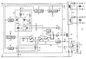
- FIG. 1schematically illustrates a portion of an embodiment of a power supply control system having a power supply controller in accordance with the present invention
- FIG. 2is a graph illustrating plots of various signals of the power supply controller of FIG. 1 in accordance with the present invention
- FIG. 3schematically illustrates an alternate embodiment of the power supply control system of FIG. 1 in accordance with the present invention
- FIG. 4schematically illustrates another alternate embodiment of the power supply control system of FIG. 1 in accordance with the present invention.
- FIG. 5schematically illustrates an enlarged plan view of a semiconductor device that includes the power supply controller of FIG. 1 in accordance with the present invention.
- current carrying electrodemeans an element of a device that carries current through the device such as a source or a drain of an MOS transistor or an emitter or a collector of a bipolar transistor or a cathode or anode of a diode
- a control electrodemeans an element of the device that controls current through the device such as a gate of an MOS transistor or a base of a bipolar transistor.
- FIG. 1schematically illustrates a portion of an embodiment of a power supply control system 10 that includes a switching power supply controller 30 .
- Controller 30is formed to include a soft-start circuit that reduces audible noise during the soft-start portion of the operation of controller 30 and system 10 .
- System 10receives power, such as a rectified dc voltage, between a power input terminal 11 and a power return terminal 12 and forms a regulated output voltage between an output 13 and an output return 14 .
- System 10generally includes a transformer 17 that generally has a primary side connected to receive the voltage from terminal 11 , a secondary connected to supply power to a load (not shown) connected between output 13 and return 14 , and an auxiliary winding that is used to supply a lower voltage power source between return 12 and an output that is connected to a voltage input 75 of controller 30 .
- a power switch or power transistor 26 of system 10is connected to the primary of transformer 17 in order to control a switch current 28 that flows through transformer 17 .
- System 10also typically includes a current sense resistor 27 , a blocking diode 18 , an output storage capacitor 19 , an opto coupler 22 , and a zener diode 23 .
- Coupler 22is connected to receive the voltage on output 13 and provide a feedback (FB) signal on an output of coupler 22 that is representative of the value of the voltage between output 13 and return 14 .
- FBfeedback
- coupler 22 and diode 23may, be replaced by other feedback circuits that are well-known to those skilled in the art.
- Resistor 27receives current 28 from transistor 26 and forms a current sense signal that is representative of current 28 .
- Transistor 26 and resistor 27typically are external to controller 30 but may be included within controller 30 in other embodiments.
- Controller 30generally includes a clock 70 , a switch control latch 32 , a transistor driver 31 , a leading edge blanking (LEB) circuit or LEB 50 , a current control comparator 38 , an error amplifier 41 , a voltage reference or reference 43 , an internal regulator or regulator 71 , a start-up circuit or start-up 44 , a first pulse width controller 54 , a second pulse width controller 47 , a first ramp generator or ramp 53 , a second ramp generator or ramp 46 , an OR gate 33 , and an inverter 35 . Controllers 54 and 47 form the soft-start circuit of controller 30 .
- the soft-start circuitis configured to control the width of the pulses of current 28 to initially start small and to gradually increase independently of the value of current 28 , and preferably non-linearly with respect to time, during a first portion of the soft-start operation period and to increase dependently of current 28 , and preferably linearly, during a second portion of the soft-start operation period in order to minimize audible noise during the soft-start period of operation.
- current 28is controlled as a function of time during the first portion of the soft-start operation period.
- the soft-start circuitmay be configured to control current 28 linearly and independently of current 28 during the first portion of the soft-start operation period.
- Controller 30is operably configured to receive power between voltage input 75 and a voltage return 76 and responsively generate a switching drive signal on a switching output 77 that controls the operation of transistor 26 .
- Regulator 71is connected between input 75 and return 76 in order to receive the input voltage and generate an internal operating voltage, on an output 72 , for operating the elements of controller 30 such as latch 32 , gate 33 , inverter 35 , comparator 38 , and amplifier 41 .
- Start-up 44is also connected between input 75 and return 76 in order to receive the input voltage and supply a control signal to regulator 71 and ramps 46 and 53 that inhibits the operation of controller 30 and ramps 46 and 53 until the value of the input voltage between input 75 and return 76 has reached a value that is sufficient to ensure proper operation of the elements of controller 30 .
- Circuits such as start-up 44are well-known to those skilled in the art. An example of such a circuit is disclosed in U.S. Pat. No. 5,477,175 that issued to Tisinger on Dec. 19, 1995 which is hereby incorporated herein by reference. An example of a circuit that includes a similar start-up function is the NCP1203 from ON Semiconductor of Phoenix Ariz.
- controller 30may include other circuits that form other functions that are not shown in FIG. 1 such as under-voltage lock-out, over-voltage protection, brown-out protection, and other well known controller functions.
- controller 54is formed to receive a control signal and responsively generate a delay with a period of the delay increasing non-linearly over time for each successive activation of the control signal.
- Controller 54includes a current source 56 , a first transistor 61 and a second transistor 62 that are configured as a differential pair, a timing capacitor 63 , a reset transistor 67 , a reset input 55 , a disable output 64 , and resistors 57 and 58 that are configured to provide a reference voltage on a reference node 59 .
- Resistors 57 and 58form a reference voltage that is applied to transistor 61 .
- resistors 57 and 58may be replaced by any circuit that provides a reference that applies the desired reference voltage to transistor 61 .
- the value of the reference voltage and the value of the output of ramp 53determine the amount of current from source 56 that is conducted through transistor 62 .
- the output of ramp 53starts at a low value, substantially equal to the value of return 76 , and increases over time.
- transistor 62conducts less current, thus, the value of a current 65 that flows through transistor 62 decreases over time.
- transistor 61conducts the majority of the current from source 56 which decreases current 65 even further and greatly increases the amount of time required to charge capacitor 63 .
- the gate-to-source voltage of transistor 62is determined by the value of the output of ramp 53 . As shown by the equation, as the gate-to-source voltage of transistor 62 varies the value of current 65 varies non-linearly due to the second order quadratic nature of the equation. Those skilled in the art will appreciate that circuits that implement other non-linear and other quadratic equations or parabolic equations or hyperbolic equations or even linear equations may be used.
- the reference voltage applied to transistor 61 by resistors 57 and 58determines the amount of current from source 56 that is conducted through transistor 62 based on the voltage from ramp 53 . Once the voltage from ramp 53 is greater than the reference voltage, transistor 61 conducts the majority of the current from source 56 .
- Controller 47includes a shunt regulator 48 that regulates the value of the voltage on an output 49 of controller 47 . If the value of ramp 46 is approximately zero, the output of regulator 48 and output 49 is at a minimum voltage value (Vm) that is set by the output structure of regulator 48 . Typically, Vm is about eighty to ninety (80-90) milli-volts greater than return 76 . As the value of ramp 46 increases past Vm, the output of regulator 48 begins to increase with a slope similar to the slope of ramp 46 . The output of regulator 48 increases until reaching a maximum output value (Vz) and regulator 48 clamps output 49 to a clamp voltage Vz. Typically, Vz is about one volt (1 V) greater than return 76 .
- Such shunt regulators and the operation thereofare well known to those skilled in the art.
- One example of such a shunt regulatoris a TL431 sold by ON Semiconductor of Phoenix Ariz.
- the value of output 49is the result of either the minimum voltage delivered by regulator 48 (Vm), or the voltage provided by the output of amplifier 41 , or the maximum voltage delivered by regulator 48 (Vz). If the output of amplifier 41 is less than the output of regulator 48 , output 49 follows the output of amplifier 41 . This case corresponds to controller 30 entering into closed loop regulation through the feedback loop. If the output of amplifier 41 is greater than the output of regulator 48 , regulator 48 clamps output 49 to the value of the output of regulator 48 .
- FIG. 2is a graph illustrating plots of various signals within controller 30 .
- the abscissaindicates increasing time and the ordinate indicates, in a general manner, the value of the signal.
- a plot 81illustrates a clock signal (CLK) on the output of clock 70
- a plot 82illustrates the value of current 65 of soft-start controller 54
- a plot 83illustrates in a general manner the width of a disable signal on output 64 of controller 54
- a plot 84illustrates the switching output signal on output 77
- a plot 86illustrates the signal on output 49 of controller 47
- a plot 87illustrates the current sense signal on output 51 of LEB 50
- a plot 89illustrates the signal on output 39 of comparator 38 .
- This descriptionhas references to both FIG. 1 and FIG. 2 .
- output storage capacitor 19When power is first applied between terminals 11 and 12 , output storage capacitor 19 typically is discharged and the output voltage between output 13 and return 14 typically is approximately zero. Additionally, the voltage on output 72 of regulator 71 is also approximately zero (approximately the value of return 76 ). As the value of the voltage between terminals 11 and 12 increases, start-up 44 receives the input voltage and typically supplies a current to regulator 71 to facilitate regulator 71 creating the internal operating voltage on output 72 . Prior to a time T 0 (see FIG. 2 ), regulator 71 is not yet supplying the internal operating voltage to operate controller 30 , the output of ramps 46 and 53 are both approximately zero (approximately equal to the value of return 76 ), latch 32 is reset, and output 77 is approximately zero.
- the low voltage from the output of ramp 53enables transistor 62 to conduct a large value of current from current source 56 . Since transistor 67 is enabled, current 65 does not charge capacitor 63 but is conducted or steered by transistor 67 to return 76 .
- the low output of ramp 46has no effect on output 49 of controller 47 because the output of regulator 48 has clamped output 49 to approximately Vm as described previously.
- capacitor 63charges to Vth before the value of current 28 increases to a value that causes output 51 of LEB 50 to reach the value on output 49 of controller 47 , thus, output 39 of comparator 38 is unaffected by current 28 .
- Capacitor 63charges to Vth and gate 33 forces the reset input of latch 32 high to force output 77 low and begin disabling transistor 26 .
- the low from output 77forces input 55 high thereby enabling transistor 67 to again discharge capacitor 63 and pull output 64 low.
- This same sequenceoccurs at a time T 2 .
- the output of ramp 53has increased further and the period of the delay time further increases non-linearly as a function of time.
- controller 54controls the width of the pulses of the switching drive signal on output 77 , thus the width of the pulses of current 28 , independently of the value of current 28 .
- controller 54 illustrated in FIG. 2is configured to increase the width of successive pulses of the switching drive signal, thus the width of the pulses of current 28 , non-linearly as a function of time.
- the width of the pulses of current 28are controlled by the value of current 28 and the width of the pulses of current 28 is increased based upon the shape, preferably linearly, of ramp 46 until the output of regulator 49 reaches Vz. As before, the low from output 77 forces input 55 high to reset controller 54 .
- clock 70once again forces CLK high to set latch 32 and force output 77 high to begin enabling transistor 26 .
- the high on output 77forces input 55 low and allows current 65 to begin charging capacitor 63 .
- the value of ramp 53has increased further, the value of current 65 has further decreased non-linearly as illustrated by plot 82 just after time T 4 .
- the soft-start period of operation of controller 30ends and the operation of controller 30 is controlled the closed control loop of clock 70 , latch 32 , driver 31 , the feedback signal received by amplifier 41 from input 79 , and the current sense signal receive on input 78 .
- the soft-start period of operationincludes a first operation period for increasing the width of the pulses of the switching control signal, thus the pulses of switch current 28 , independently of current 28 and preferably non-linearly as a function of time and a second operation period for increasing the width of the switching control signal, thus the pulses of switch current 28 , as a function, preferably linearly, of current 28 .
- the width of the switching control signal pulses during the first operation periodbegin very small and increase typically with each successive pulse.
- Prior art controllers without controller 54have a large initial pulse width that causes audible noise.
- Controller 54is formed to generate initial pulses with a small width and increase the width in order to minimize audible noise.
- terminal 11is connected to a first terminal of transformer 17
- terminal 12is connected to both return 76 , a return terminal of the auxiliary winding of transformer 17 , and a first terminal of resistor 27 .
- a second terminal of resistor 27is connected to input 78 and to a source of transistor 26 .
- a gate of transistor 26is connected to output 77 , and a drain is connected to a second terminal of transformer 17 .
- Input 75is connected to a second terminal of the auxiliary winding of transformer 17 , an input of regulator 71 , and an input of start-up 44 .
- a first output of start-up 44is connected to a control input of regulator 71 , and a second output of start-up 44 is commonly connected to a control input of ramps 46 and 53 .
- the CLK output of clock 70is connected to the set input of latch 32 , and a Q output of latch 32 is connected to an input of driver 31 .
- An output of driver 31is connected to output 77 and to an input of inverter 35 .
- An output of inverter 35is connected to input 55 of controller 54 .
- Output 64 of controller 54is connected to a first input of gate 33 which has an output connected to the reset input of latch 32 .
- Input 55is connected to a gate of transistor 67 which has a source commonly connected to return 76 , a drain of transistor 61 and a first terminal of capacitor 63 .
- a second terminal of capacitor 63is commonly connected to a drain of transistor 62 , a drain of transistor 67 , and output 64 .
- a source of transistor 62is commonly connected to a source of transistor 61 and to an output terminal of source 56 .
- a gate of transistor 62is connected to an output of ramp 53 .
- a gate of transistor 61is commonly connected to a first terminal of resistors 57 and 58 .
- a second terminal of resistor 58is connected to return 76 .
- a second terminal of resistor 57is commonly connected to output 72 of regulator 71 and an input terminal of source 56 .
- An inverting input of amplifier 41is connected to an output of reference 43 .
- a non-inverting input of amplifier 41is connected to a first terminal of a resistor 69 and to a first terminal of a resistor 68 which has a second terminal commonly connected to input 79 of controller 30 and to a first terminal of a resistor 42 .
- a second terminal of resistor 69is connected to the output of amplifier 41 .
- a second terminal of resistor 42is connected to output 72 of regulator 71 .
- the output of amplifier 41is commonly connected to a non-inverting input of comparator 38 and output 49 of controller 47 .
- a first terminal of regulator 48is connected to return 76 , a second terminal of regulator 48 is connected to output 49 , and a control terminal is connected to the output of ramp 46 .
- An inverting input of comparator 38is connected to output 51 of LEB 50 which has an input connected to input 78 of controller 30 .
- Output 39 of comparator 38is connected to a second input of gate
- FIG. 3schematically illustrates a portion of an embodiment of a power supply control system 93 that includes a switching power supply controller 94 .
- System 93 and controller 94are alternate embodiments of respective system 10 and controller 30 explained in the description of FIG. 1 and FIG. 2 .
- Controller 94is similar to controller 30 except that ramp 53 is used to form the ramp signal for both controller 54 and controller 47 .
- FIG. 4schematically illustrates a portion of an embodiment of a power supply control system 100 that includes a switching power supply controller 101 .
- System 100 and controller 101are alternate embodiments of respective system 10 and controller 30 explained in the description of FIG. 1 and FIG. 2 .
- Controller 101is similar to controller 30 except that controller 101 includes a burst-mode or skip-mode comparator 106 , an inverter 107 , and an OR gate 108 that facilitates operating controller 101 in a low power burst-mode or skip-mode that includes soft-start operation.
- Controller 101also includes a reference generator of reference 104 that is similar to reference 43 except that reference 104 forms a second reference voltage (Vref 2 ) on a second output that is used to facilitate the skip-mode.
- Vref 2second reference voltage
- the output of comparator 106is forced high to reset latch 32 through gate 103 thereby inhibiting switching of transistor 26 and entering the skip-mode. As a result, the value of the output voltage decreases and correspondingly increases the value of the FB signal. If FB becomes greater than the sum of Vref 2 plus the hysteresis of comparator 106 , the output of comparator 106 is forced low to release latch 32 and allow CLK to set latch 32 .
- the low from comparator 106also forces the output of gate 108 high to start a ramp generation cycle from ramps 46 and 53 thereby beginning a soft-start operation that controls the width of the pulses the switching control signal and the corresponding pulses of current 28 as described hereinbefore in the description of FIG. 1 and FIG. 2 .
- the soft-start operationis useful for minimizing audible noise at start-up and also when transition from a skip-mode to a closed loop operating mode.
- FIG. 5schematically illustrates an enlarged plan view of a portion of an embodiment of a semiconductor device 98 that is formed on a semiconductor die 99 .
- Controller 30is formed on die 99 .
- Die 99may also include other circuits that are not shown in FIG. 4 for simplicity of the drawing.
- Controller 30 and device 98are formed on die 99 by semiconductor manufacturing techniques that are well known to those skilled in the art.
- a novel device and methodis disclosed. Included, among other features, is forming a soft-start period of operation including a first operation period for increasing the width of the pulses of switch current 28 independently of the value of the switch current and preferably non-linearly as a function of time, and a second operation period for increasing the width of the switch current pulses as a function of the value of the switch current and preferably linearly.
- the width of the switching pulses during the first operation periodhave a small width in order to minimize audible noise.
Landscapes
- Engineering & Computer Science (AREA)
- Power Engineering (AREA)
- Dc-Dc Converters (AREA)
- Motor And Converter Starters (AREA)
- Inverter Devices (AREA)
Abstract
Description
I65=0.5*Mp*Cx*W*((V62gs−V62th)2/L)
- Where:
- I65=the value of current65,
- Mp=hole mobility,
- Cx=Capacitance of gate insulator of
transistor 62, - V62gs=gate to source voltage of
transistor 62, - V62th=the threshold voltage of
transistor 62, - W=the width of
transistor 62, and - L=the channel length of
transistor 62.
Claims (20)
Applications Claiming Priority (1)
| Application Number | Priority Date | Filing Date | Title |
|---|---|---|---|
| PCT/US2005/003396WO2006085847A1 (en) | 2005-01-28 | 2005-01-28 | Soft-start circuit and method therefor |
Publications (2)
| Publication Number | Publication Date |
|---|---|
| US20080246450A1 US20080246450A1 (en) | 2008-10-09 |
| US7719249B2true US7719249B2 (en) | 2010-05-18 |
Family
ID=35134415
Family Applications (1)
| Application Number | Title | Priority Date | Filing Date |
|---|---|---|---|
| US11/576,174Active2025-11-08US7719249B2 (en) | 2005-01-28 | 2005-01-28 | Soft-start circuit and method therefor |
Country Status (4)
| Country | Link |
|---|---|
| US (1) | US7719249B2 (en) |
| CN (1) | CN101073196B (en) |
| TW (1) | TWI389440B (en) |
| WO (1) | WO2006085847A1 (en) |
Cited By (13)
| Publication number | Priority date | Publication date | Assignee | Title |
|---|---|---|---|---|
| US20090206920A1 (en)* | 2008-02-19 | 2009-08-20 | Chao-Cheng Lee | Soft-start device |
| US20090261797A1 (en)* | 2008-04-22 | 2009-10-22 | Seiko Instruments Inc. | Switching regulator |
| US20100156382A1 (en)* | 2008-12-19 | 2010-06-24 | Ricoh Company, Ltd. | Soft-start circuit and power supply circuit including same |
| US20110309812A1 (en)* | 2010-06-18 | 2011-12-22 | Miller Ira G | Switching regulator with input current limiting capabilities |
| US20130100714A1 (en)* | 2011-10-20 | 2013-04-25 | Power Integrations, Inc. | Power controller with smooth transition to pulse skipping |
| CN103092243A (en)* | 2011-11-07 | 2013-05-08 | 联发科技(新加坡)私人有限公司 | Signal generating circuit |
| US20160336852A1 (en)* | 2015-05-15 | 2016-11-17 | On-Bright Electronics (Shanghai) Co., Ltd. | Systems and Methods for Output Current Regulation in Power Conversion Systems |
| US9991802B2 (en) | 2014-04-18 | 2018-06-05 | On-Bright Electronics (Shanghai) Co., Ltd. | Systems and methods for regulating output currents of power conversion systems |
| US10003268B2 (en) | 2015-05-15 | 2018-06-19 | On-Bright Electronics (Shanghai) Co., Ltd. | Systems and methods for output current regulation in power conversion systems |
| US10170999B2 (en) | 2014-04-18 | 2019-01-01 | On-Bright Electronics (Shanghai) Co., Ltd. | Systems and methods for regulating output currents of power conversion systems |
| US10177665B2 (en) | 2013-07-19 | 2019-01-08 | On-Bright Electronics (Shanghai) Co., Ltd. | Systems and methods for high precision and/or low loss regulation of output currents of power conversion systems |
| US10211626B2 (en) | 2015-02-02 | 2019-02-19 | On-Bright Electronics (Shanghai) Co., Ltd. | System and method providing reliable over current protection for power converter |
| US10277110B2 (en) | 2010-12-08 | 2019-04-30 | On-Bright Electronics (Shanghai) Co., Ltd. | System and method providing over current protection based on duty cycle information for power converter |
Families Citing this family (15)
| Publication number | Priority date | Publication date | Assignee | Title |
|---|---|---|---|---|
| CN101218737A (en)* | 2005-05-10 | 2008-07-09 | Nxp股份有限公司 | Feedback communication technique for switched mode power supply |
| JP2010166019A (en)* | 2008-12-18 | 2010-07-29 | Panasonic Corp | Semiconductor laser device |
| US7990196B2 (en)* | 2009-12-22 | 2011-08-02 | Toshiba America Electronic Components, Inc. | Signal driver with first pulse boost |
| TWI427910B (en)* | 2010-03-09 | 2014-02-21 | Monolithic Power Systems Inc | Switching mode power supply with a multi-mode controller |
| US8976981B2 (en)* | 2010-10-07 | 2015-03-10 | Blackberry Limited | Circuit, system and method for isolating a transducer from an amplifier in an electronic device |
| US9948175B2 (en)* | 2010-10-25 | 2018-04-17 | Analog Devices, Inc. | Soft-start control system and method for an isolated DC-DC converter with secondary controller |
| US9048747B2 (en)* | 2011-11-23 | 2015-06-02 | Zahid Ansari | Switched-mode power supply startup circuit, method, and system incorporating same |
| CN103248238A (en)* | 2012-02-07 | 2013-08-14 | 广州金升阳科技有限公司 | Ringing choke converter |
| US9293997B2 (en) | 2013-03-14 | 2016-03-22 | Analog Devices Global | Isolated error amplifier for isolated power supplies |
| TWI497894B (en)* | 2013-12-03 | 2015-08-21 | Grenergy Opto Inc | Power controller and relevant control method for operating a power supply to switch at a bottom of a voltage valley |
| CN105490533B (en)* | 2014-10-11 | 2019-07-09 | 意法半导体研发(深圳)有限公司 | Switching Converter for Operation in Pulse Width Modulation Mode or Pulse Skip Mode |
| KR20160070710A (en)* | 2014-12-10 | 2016-06-20 | 페어차일드코리아반도체 주식회사 | Modulation mode control circuit, switch control circuit comprising the same, and power supply device comprising the switch control circuit |
| CN105807834B (en) | 2014-12-29 | 2018-05-08 | 意法半导体(中国)投资有限公司 | N-Channel Input-Pair Voltage Regulator with Soft-Start and Current Limit Circuitry |
| CN109997303B (en)* | 2017-11-03 | 2021-02-12 | 戴洛格半导体(英国)有限公司 | Switch driver |
| TWI686039B (en)* | 2018-12-27 | 2020-02-21 | 大陸商北京集創北方科技股份有限公司 | Constant current soft start control circuit and power management chip using the same |
Citations (4)
| Publication number | Priority date | Publication date | Assignee | Title |
|---|---|---|---|---|
| US3746970A (en)* | 1972-04-13 | 1973-07-17 | Ibm | Root mean square voltage regulator |
| US5502370A (en)* | 1994-09-06 | 1996-03-26 | Motorola, Inc. | Power factor control circuit having a boost current for increasing a speed of a voltage control loop and method therefor |
| US5917313A (en)* | 1997-12-19 | 1999-06-29 | Stmicroelectronics, Inc. | DC-to-DC converter with soft-start error amplifier and associated method |
| US6377480B1 (en)* | 2001-01-18 | 2002-04-23 | Hitachi, Ltd. | Soft start circuit for switching power supply |
Family Cites Families (3)
| Publication number | Priority date | Publication date | Assignee | Title |
|---|---|---|---|---|
| NL8900508A (en)* | 1989-03-02 | 1990-10-01 | Philips Nv | SWITCHED POWER SUPPLY SWITCH WITH START-UP SWITCH. |
| WO2003001314A1 (en)* | 2001-06-21 | 2003-01-03 | Champion Microelectronic Corp. | Current limiting technique for a switching power converter |
| JP4082200B2 (en)* | 2002-12-12 | 2008-04-30 | 株式会社豊田自動織機 | DC-DC converter |
- 2005
- 2005-01-28USUS11/576,174patent/US7719249B2/enactiveActive
- 2005-01-28CNCN200580041731.XApatent/CN101073196B/ennot_activeExpired - Fee Related
- 2005-01-28WOPCT/US2005/003396patent/WO2006085847A1/enactiveApplication Filing
- 2005-12-07TWTW094143241Apatent/TWI389440B/enactive
Patent Citations (4)
| Publication number | Priority date | Publication date | Assignee | Title |
|---|---|---|---|---|
| US3746970A (en)* | 1972-04-13 | 1973-07-17 | Ibm | Root mean square voltage regulator |
| US5502370A (en)* | 1994-09-06 | 1996-03-26 | Motorola, Inc. | Power factor control circuit having a boost current for increasing a speed of a voltage control loop and method therefor |
| US5917313A (en)* | 1997-12-19 | 1999-06-29 | Stmicroelectronics, Inc. | DC-to-DC converter with soft-start error amplifier and associated method |
| US6377480B1 (en)* | 2001-01-18 | 2002-04-23 | Hitachi, Ltd. | Soft start circuit for switching power supply |
Cited By (41)
| Publication number | Priority date | Publication date | Assignee | Title |
|---|---|---|---|---|
| US7948273B2 (en)* | 2008-02-19 | 2011-05-24 | Realtek Semiconductor Corp. | Soft-start device |
| US20090206920A1 (en)* | 2008-02-19 | 2009-08-20 | Chao-Cheng Lee | Soft-start device |
| US20090261797A1 (en)* | 2008-04-22 | 2009-10-22 | Seiko Instruments Inc. | Switching regulator |
| US7928715B2 (en)* | 2008-04-22 | 2011-04-19 | Seiko Instruments Inc. | Switching regulator |
| US20100156382A1 (en)* | 2008-12-19 | 2010-06-24 | Ricoh Company, Ltd. | Soft-start circuit and power supply circuit including same |
| US8207715B2 (en)* | 2008-12-19 | 2012-06-26 | Ricoh Company, Ltd. | Soft-start circuit and power supply circuit including same |
| US8754626B2 (en)* | 2010-06-18 | 2014-06-17 | Freescale Semiconductor, Inc. | Switching regulator with input current limiting capabilities |
| US20110309812A1 (en)* | 2010-06-18 | 2011-12-22 | Miller Ira G | Switching regulator with input current limiting capabilities |
| US10581315B2 (en) | 2010-12-08 | 2020-03-03 | On-Bright Electronics (Shanghai) Co., Ltd. | System and method providing over current protection based on duty cycle information for power converter |
| US11264888B2 (en) | 2010-12-08 | 2022-03-01 | On-Bright Electronics (Shanghai) Co., Ltd. | System and method providing over current protection based on duty cycle information for power converter |
| US10483838B2 (en) | 2010-12-08 | 2019-11-19 | On-Bright Electronics (Shanghai) Co., Ltd. | System and method providing over current protection based on duty cycle information for power converter |
| US10615684B2 (en) | 2010-12-08 | 2020-04-07 | On-Bright Electronics (Shanghai) Co., Ltd. | System and method providing over current protection based on duty cycle information for power converter |
| US10277110B2 (en) | 2010-12-08 | 2019-04-30 | On-Bright Electronics (Shanghai) Co., Ltd. | System and method providing over current protection based on duty cycle information for power converter |
| US10811955B2 (en) | 2010-12-08 | 2020-10-20 | On-Bright Electronics (Shanghai) Co., Ltd. | System and method providing over current protection based on duty cycle information for power converter |
| US11114933B2 (en) | 2010-12-08 | 2021-09-07 | On-Bright Electronics (Shanghai) Co., Ltd. | System and method providing over current protection based on duty cycle information for power converter |
| US9083251B2 (en) | 2011-10-20 | 2015-07-14 | Power Integrations, Inc. | Power controller with pulse skipping |
| US20130100714A1 (en)* | 2011-10-20 | 2013-04-25 | Power Integrations, Inc. | Power controller with smooth transition to pulse skipping |
| US8823353B2 (en)* | 2011-10-20 | 2014-09-02 | Power Integrations, Inc. | Power controller with smooth transition to pulse skipping |
| US20130113454A1 (en)* | 2011-11-07 | 2013-05-09 | Xi Chen | Signal generating circuit |
| TWI486739B (en)* | 2011-11-07 | 2015-06-01 | Mediatek Singapore Pte Ltd | Signal generating circuit |
| US9000742B2 (en)* | 2011-11-07 | 2015-04-07 | Mediatek Singapore Pte. Ltd. | Signal generating circuit |
| CN103092243A (en)* | 2011-11-07 | 2013-05-08 | 联发科技(新加坡)私人有限公司 | Signal generating circuit |
| US10177665B2 (en) | 2013-07-19 | 2019-01-08 | On-Bright Electronics (Shanghai) Co., Ltd. | Systems and methods for high precision and/or low loss regulation of output currents of power conversion systems |
| US10211740B2 (en) | 2013-07-19 | 2019-02-19 | On-Bright Electronics (Shanghai) Co., Ltd. | Systems and methods for high precision and/or low loss regulation of output currents of power conversion systems |
| US11108328B2 (en) | 2013-07-19 | 2021-08-31 | On-Bright Electronics (Shanghai) Co., Ltd. | Systems and methods for high precision and/or low loss regulation of output currents of power conversion systems |
| US10044254B2 (en) | 2014-04-18 | 2018-08-07 | On-Bright Electronics (Shanghai) Co., Ltd. | Systems and methods for regulating output currents of power conversion systems |
| US10170999B2 (en) | 2014-04-18 | 2019-01-01 | On-Bright Electronics (Shanghai) Co., Ltd. | Systems and methods for regulating output currents of power conversion systems |
| US9991802B2 (en) | 2014-04-18 | 2018-06-05 | On-Bright Electronics (Shanghai) Co., Ltd. | Systems and methods for regulating output currents of power conversion systems |
| US10686359B2 (en) | 2014-04-18 | 2020-06-16 | On-Bright Electronics (Shanghai) Co., Ltd. | Systems and methods for regulating output currents of power conversion systems |
| US10211626B2 (en) | 2015-02-02 | 2019-02-19 | On-Bright Electronics (Shanghai) Co., Ltd. | System and method providing reliable over current protection for power converter |
| US10270334B2 (en)* | 2015-05-15 | 2019-04-23 | On-Bright Electronics (Shanghai) Co., Ltd. | Systems and methods for output current regulation in power conversion systems |
| US10432096B2 (en) | 2015-05-15 | 2019-10-01 | On-Bright Electronics (Shanghai) Co., Ltd. | Systems and methods for output current regulation in power conversion systems |
| US10680525B2 (en) | 2015-05-15 | 2020-06-09 | On-Bright Electronics (Shanghai) Co., Ltd. | Systems and methods for output current regulation in power conversion systems |
| US10686373B2 (en) | 2015-05-15 | 2020-06-16 | On-Bright Electronics (Shanghai) Co., Ltd. | Systems and methods for output current regulation in power conversion systems |
| US10340795B2 (en) | 2015-05-15 | 2019-07-02 | On-Bright Electronics (Shanghai) Co., Ltd. | Systems and methods for output current regulation in power conversion systems |
| US10811965B2 (en) | 2015-05-15 | 2020-10-20 | On-Bright Electronics (Shanghai) Co., Ltd. | Systems and methods for output current regulation in power conversion systems |
| US10003268B2 (en) | 2015-05-15 | 2018-06-19 | On-Bright Electronics (Shanghai) Co., Ltd. | Systems and methods for output current regulation in power conversion systems |
| US9960674B2 (en)* | 2015-05-15 | 2018-05-01 | On-Bright Electronics (Shanghai) Co., Ltd. | Systems and methods for output current regulation in power conversion systems |
| US20160336868A1 (en)* | 2015-05-15 | 2016-11-17 | On-Bright Electronics (Shanghai) Co., Ltd. | Systems and methods for output current regulation in power conversion systems |
| US20160336852A1 (en)* | 2015-05-15 | 2016-11-17 | On-Bright Electronics (Shanghai) Co., Ltd. | Systems and Methods for Output Current Regulation in Power Conversion Systems |
| US11652410B2 (en) | 2015-05-15 | 2023-05-16 | On-Bright Electronics (Shanghai) Co., Ltd. | Systems and methods for output current regulation in power conversion systems |
Also Published As
| Publication number | Publication date |
|---|---|
| CN101073196B (en) | 2012-01-11 |
| CN101073196A (en) | 2007-11-14 |
| TW200635193A (en) | 2006-10-01 |
| HK1113521A1 (en) | 2008-10-03 |
| WO2006085847A1 (en) | 2006-08-17 |
| TWI389440B (en) | 2013-03-11 |
| US20080246450A1 (en) | 2008-10-09 |
Similar Documents
| Publication | Publication Date | Title |
|---|---|---|
| US7719249B2 (en) | Soft-start circuit and method therefor | |
| KR101912211B1 (en) | Soft start circuits and techniques | |
| TWI385494B (en) | Soft start circuit, power supply controller, and method therefor | |
| US6980444B2 (en) | Switching power supply | |
| US7477532B2 (en) | Method of forming a start-up device and structure therefor | |
| US7646184B2 (en) | Method and apparatus for maintaining a constant load current with line voltage in a switch mode power supply | |
| US6057675A (en) | DC/DC converter | |
| US7787269B2 (en) | Switching power supply device | |
| US7723972B1 (en) | Reducing soft start delay and providing soft recovery in power system controllers | |
| US5710697A (en) | Power supply controller having frequency foldback and volt-second duty cycle clamp features | |
| US7486529B2 (en) | Switching power supply controller with improved efficiency and method therefor | |
| US7558084B2 (en) | Switching mode power supply with compensated propagation delay | |
| US10601329B2 (en) | Switching regulator and power switch controller circuit thereof | |
| US12323066B2 (en) | Systems and methods for controlling gate voltage increase on primary side to reduce voltage spike on secondary side of switching power supplies | |
| US7212416B2 (en) | Switching power supply device and switching method | |
| US20180123581A1 (en) | Control circuit and method therefor | |
| KR20110095771A (en) | Switch control device, power supply and switch control method comprising the same | |
| US10038385B2 (en) | Flyback converter and controller using counter and current emulator | |
| KR101021993B1 (en) | Switching mode power supplies and their switching controls | |
| US7515442B2 (en) | Secondary side controller and method therefor | |
| US8174243B2 (en) | Power supply controller and method therefor | |
| US20050068085A1 (en) | Hot swappable pulse width modulation power supply circuits | |
| US7457138B2 (en) | Single pin multi-function signal detection method and structure therefor | |
| HK1113521B (en) | Soft-start circuit and method therefor | |
| JP2006158091A (en) | Switching power supply |
Legal Events
| Date | Code | Title | Description |
|---|---|---|---|
| AS | Assignment | Owner name:SEMICONDUCTOR COMPONENTS INDUSTRIES, L.L.C., ARIZO Free format text:ASSIGNMENT OF ASSIGNORS INTEREST;ASSIGNORS:MATYAS, LADISLAV;LHERMITE, FRANCOIS;REEL/FRAME:016342/0306;SIGNING DATES FROM 20050118 TO 20050119 Owner name:SEMICONDUCTOR COMPONENTS INDUSTRIES, L.L.C.,ARIZON Free format text:ASSIGNMENT OF ASSIGNORS INTEREST;ASSIGNORS:MATYAS, LADISLAV;LHERMITE, FRANCOIS;SIGNING DATES FROM 20050118 TO 20050119;REEL/FRAME:016342/0306 | |
| AS | Assignment | Owner name:JPMORGAN CHASE BANK, N.A., NEW YORK Free format text:SECURITY AGREEMENT;ASSIGNOR:SEMICONDUCTOR COMPONENTS INDUSTRIES, LLC;REEL/FRAME:019795/0808 Effective date:20070906 Owner name:JPMORGAN CHASE BANK, N.A.,NEW YORK Free format text:SECURITY AGREEMENT;ASSIGNOR:SEMICONDUCTOR COMPONENTS INDUSTRIES, LLC;REEL/FRAME:019795/0808 Effective date:20070906 | |
| STCF | Information on status: patent grant | Free format text:PATENTED CASE | |
| FPAY | Fee payment | Year of fee payment:4 | |
| AS | Assignment | Owner name:SEMICONDUCTOR COMPONENTS INDUSTRIES, LLC, ARIZONA Free format text:RELEASE OF SECURITY INTEREST;ASSIGNOR:JPMORGAN CHASE BANK, N.A.;REEL/FRAME:033686/0092 Effective date:20100511 | |
| MAFP | Maintenance fee payment | Free format text:PAYMENT OF MAINTENANCE FEE, 8TH YEAR, LARGE ENTITY (ORIGINAL EVENT CODE: M1552) Year of fee payment:8 | |
| AS | Assignment | Owner name:DEUTSCHE BANK AG NEW YORK BRANCH, AS COLLATERAL AGENT, NEW YORK Free format text:SECURITY INTEREST;ASSIGNORS:SEMICONDUCTOR COMPONENTS INDUSTRIES, LLC;FAIRCHILD SEMICONDUCTOR CORPORATION;ON SEMICONDUCTOR CONNECTIVITY SOLUTIONS, INC.;REEL/FRAME:054090/0617 Effective date:20200213 | |
| MAFP | Maintenance fee payment | Free format text:PAYMENT OF MAINTENANCE FEE, 12TH YEAR, LARGE ENTITY (ORIGINAL EVENT CODE: M1553); ENTITY STATUS OF PATENT OWNER: LARGE ENTITY Year of fee payment:12 | |
| AS | Assignment | Owner name:FAIRCHILD SEMICONDUCTOR CORPORATION, ARIZONA Free format text:RELEASE OF SECURITY INTEREST IN PATENTS RECORDED AT REEL 054090, FRAME 0617;ASSIGNOR:DEUTSCHE BANK AG NEW YORK BRANCH, AS COLLATERAL AGENT;REEL/FRAME:064081/0167 Effective date:20230622 Owner name:SEMICONDUCTOR COMPONENTS INDUSTRIES, LLC, ARIZONA Free format text:RELEASE OF SECURITY INTEREST IN PATENTS RECORDED AT REEL 054090, FRAME 0617;ASSIGNOR:DEUTSCHE BANK AG NEW YORK BRANCH, AS COLLATERAL AGENT;REEL/FRAME:064081/0167 Effective date:20230622 |