US7715203B2 - RF module structure of a mobile communication terminal - Google Patents
RF module structure of a mobile communication terminalDownload PDFInfo
- Publication number
- US7715203B2 US7715203B2US11/026,080US2608004AUS7715203B2US 7715203 B2US7715203 B2US 7715203B2US 2608004 AUS2608004 AUS 2608004AUS 7715203 B2US7715203 B2US 7715203B2
- Authority
- US
- United States
- Prior art keywords
- communication terminal
- mobile communication
- radio frequency
- mcm
- board
- Prior art date
- Legal status (The legal status is an assumption and is not a legal conclusion. Google has not performed a legal analysis and makes no representation as to the accuracy of the status listed.)
- Expired - Fee Related, expires
Links
Images


Classifications
- H—ELECTRICITY
- H04—ELECTRIC COMMUNICATION TECHNIQUE
- H04B—TRANSMISSION
- H04B1/00—Details of transmission systems, not covered by a single one of groups H04B3/00 - H04B13/00; Details of transmission systems not characterised by the medium used for transmission
- H04B1/38—Transceivers, i.e. devices in which transmitter and receiver form a structural unit and in which at least one part is used for functions of transmitting and receiving
- H04B1/40—Circuits
- H—ELECTRICITY
- H04—ELECTRIC COMMUNICATION TECHNIQUE
- H04B—TRANSMISSION
- H04B1/00—Details of transmission systems, not covered by a single one of groups H04B3/00 - H04B13/00; Details of transmission systems not characterised by the medium used for transmission
- H04B1/38—Transceivers, i.e. devices in which transmitter and receiver form a structural unit and in which at least one part is used for functions of transmitting and receiving
Definitions
- the present inventionrelates to a structure having a radio frequency multi-chip module that is replaceable from the RF portion of a mobile communication terminal.
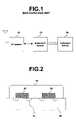
- FIG. 1is a block diagram of a general mobile communication terminal.
- a mobile communication terminalincludes a radio frequency (RF) system 10 , a base-band system 20 , and a peripheral device 30 .
- RFradio frequency
- the RF system 10provides an antenna, a transmission unit, a reception unit and a local oscillator (LO).
- the base-band system 20has a mobile station modem (MSM) chip corresponding to a central processing unit (CPU) of a computer.
- MSMmobile station modem
- CPUcentral processing unit
- the base-band systemalso provides a memory and peripheral devices.
- the peripheral device 30provides a user with an output signal of the base-band system 20 or transmits a signal inputted by a user to the base-band system 20 .
- the peripheral device 30generally includes a speaker, a microphone, a keypad, a liquid crystal display (LCD), a camera or the like.
- the RF system 10 and the base-band system 20are integrated on a single board.
- a module structure of a mobile communication terminalcomprises a radio frequency portion for processing communicated radio frequency signals, and a base-band portion commonly used by the radio frequency portion for providing modular replacement of a radio frequency multi-chip module connected to the radio frequency portion.
- the radio frequency multi-chip moduleis selected in accordance with a corresponding frequency band of the mobile communication terminal.
- the RF multi-chip modulemay be implemented utilizing a lead free type of interconnection scheme with the base-band portion.
- the RF multi-chip modulemay, in another example, be implemented utilizing a lead type of electrical interconnection scheme with the base-band portion.
- the RF multi-chip modulemay be implemented utilizing a connector type of electrical interconnection scheme with the base-band portion.
- the RF multi-chip modulepreferably comprises a board, a plurality of RF components mounted on the board, and a cap for isolating the RF components from the exterior environment from electrical interference signals.
- the boardis preferably a ceramic laminated board.
- FIG. 1is block diagram illustrating a conventional configuration of a mobile communication terminal.
- FIG. 2is a cross-sectional view of an RF multi-chip module in accordance with an embodiment of the present invention.
- FIG. 3is an RF package layout showing various types of connection terminals of a RF multi-chip module in accordance with an embodiment of the present invention.
- the inventionrelates to a module structure having a radio frequency multi-chip module that may be modularly replaceable from the RF portion of the module structure for a mobile communication terminal.
- the present inventionprovides an RF multi-chip module (MCM) with is part of a modularized RF portion of a mobile communication terminal.
- MCMRF multi-chip module
- the RF portionis integrated, on the mobile terminal, with a base-band portion into one chip.
- a base-band portionis commonly used with a chipset and a desired RF MCM is replaceably inserted thereto according to the frequency utilized in the specific area, so that a mobile communication terminal may be easily fabricated in a short period of time without the need for designing a new RF board.
- FIG. 2is a cross-sectional view of an RF MCM in accordance with an embodiment of the present invention.
- a plurality of wiresare formed on an upper surface of a board 50 for allowing transfer of signals.
- a transmission unit 52 and a reception unit 53are separately mounted on the board 50 .
- a cap 54provides signal isolation of the transmission unit 52 and the reception unit 53 from the exterior environment (not shown).
- the board 50may be formed by a low temperature co-fired ceramic (LTCC) laminated board, a high co-fired ceramic (HTCC) laminated board, or a general FR-4 printed circuit board (PCB).
- the general FR-4 printed circuit boardmay be of a two-sided epoxy construction.
- the cap 30is implemented, in one exemplary embodiment, utilizing an epoxy molding or, in yet another example, utilizing a metal shield.
- the FR-4is preferably utilized as the material for the multi-layer board 50 of the RF MCM.
- Wires 51are mounted on a chip of the board 50 .
- Wires 51are utilized for separately mounting a transmission unit 52 and a reception unit 53 deposited on the board.
- the board 50in this exemplary example, is an LTCC.
- the LTCCis a ceramic board formed by laminating ceramic sheets.
- the LTCC having a dielectric nearly twice as high as that of FR-4reduces board dimensionality and accordingly reduces the board size. Because the LTCC has a good heat conductivity, the heat generated, for example, by a power amplifier module (PAM) may be efficiently removed from the board 50 . The reduced heating will reduce the temperature of the mobile terminal.
- PAMpower amplifier module
- FIG. 3is an RF package layout showing various connection terminals of an RF MCM in accordance with the present invention.
- the RF MCMmaybe a lead free type or a leaded type in accordance with the type of pins used for electrical interconnections the mobile terminal.
- connectorsmay be used in place of pins.
- reference number 60is a connector for a connector type RF MCM and reference number 61 is a cap.
- An RF systemmay be implemented within an RF MCM through mounting the components on a board 50 using various mounting methods such as those described in the above FIG. 2 . Operation of the RF MCM is the same as that of the RF system, and a board 50 may be utilized for the RF MCM using LTCC.
- Each componentin this example, has a bare-die state and is wire-bonded to the LTCC during fabrication of an RF MCM.
- a transmission unit 52 and a reception unit 53are positioned along the wires 51 of the board 50 . Wire-bonding is utilized to complete fabrication of the RF MCM.
- Components which have been previously modularizedare soldered to the LTCC during fabrication of an RF MCM.
- a transmission unit 52 and a reception unit 53 being previously modularizedare respectively positioned on the wires 51 and soldered to the LTCC during fabrication of an RF MCM.
- the RF MCMis covered with a cap 54 to provide isolation from an exterior environment.
- the cap 54 of the RF MCMmay fabricated either using an epoxy molding method like that of an IC package for covering the board.
- a shielded metalmay be utilized to block unwanted wave interference to increase ESD protection and GNDing affects.
- the RF portionis separately modularized in a mobile communication terminal.
- the base-band portionis commonly used by the RF portion.
- the RF moduleis replaced depending on the type of service provider, such as PCS, CDMA, Tri-Mode or the like. The replacement of the RF module provides a mobile terminal with smooth frequency transitions between various frequency bands.
- an RF MCM obtained by separately modularizing an RF parteliminates the need for new circuits to be designed even in an area using a different frequency to readily reconfigure a mobile terminal in a short time period.
- the present inventionprovides a reduced board size by fabricating an RF MCM using an LTCC board having a ceramic laminated board instead of with an FR-4 board.
- the LTCC boardefficiently radiates heat generated within the board so that the overall temperature of the mobile terminal is reduced.
- the present inventionis described in the context of a mobile terminal, the present invention may also be used in any wired or wireless communication systems using mobile devices, such as PDAs and laptop computers equipped with wired and wireless communication capabilities. Moreover, the use of certain terms to describe the present invention should not limit the scope of the present invention to certain type of wireless communication system, such as UMTS. The present invention is also applicable to other wireless communication systems using different air interfaces and/or physical layers, for example, TDMA, CDMA, FDMA, WCDMA, etc.
Landscapes
- Engineering & Computer Science (AREA)
- Computer Networks & Wireless Communication (AREA)
- Signal Processing (AREA)
- Transceivers (AREA)
- Telephone Set Structure (AREA)
Abstract
Description
Claims (9)
Applications Claiming Priority (2)
| Application Number | Priority Date | Filing Date | Title |
|---|---|---|---|
| KR10-2003-0100748 | 2003-12-30 | ||
| KR1020030100748AKR100631673B1 (en) | 2003-12-30 | 2003-12-30 | High Frequency Module Structure for Mobile Communication |
Publications (2)
| Publication Number | Publication Date |
|---|---|
| US20050143122A1 US20050143122A1 (en) | 2005-06-30 |
| US7715203B2true US7715203B2 (en) | 2010-05-11 |
Family
ID=34567862
Family Applications (1)
| Application Number | Title | Priority Date | Filing Date |
|---|---|---|---|
| US11/026,080Expired - Fee RelatedUS7715203B2 (en) | 2003-12-30 | 2004-12-30 | RF module structure of a mobile communication terminal |
Country Status (6)
| Country | Link |
|---|---|
| US (1) | US7715203B2 (en) |
| EP (1) | EP1551106B1 (en) |
| KR (1) | KR100631673B1 (en) |
| CN (1) | CN1665378A (en) |
| AT (1) | ATE505851T1 (en) |
| DE (1) | DE602004032207D1 (en) |
Cited By (4)
| Publication number | Priority date | Publication date | Assignee | Title |
|---|---|---|---|---|
| US20160381808A1 (en)* | 2015-06-29 | 2016-12-29 | NagraID Security | Method of Reducing the Thickness of an Electronic Circuit |
| US12015433B2 (en)* | 2018-06-11 | 2024-06-18 | Murata Manufacturing Co., Ltd. | Radio frequency module and communication device |
| US12256486B2 (en) | 2021-06-04 | 2025-03-18 | Samsung Electronics Co., Ltd. | Shield structure in electronic device and operation method thereof |
| US12268863B2 (en) | 2023-02-06 | 2025-04-08 | Novocure Gmbh | Shiftable transducer array with anisotropic material layer |
Families Citing this family (1)
| Publication number | Priority date | Publication date | Assignee | Title |
|---|---|---|---|---|
| CN111221390A (en)* | 2019-12-31 | 2020-06-02 | 苏州浪潮智能科技有限公司 | Backboard compatible with time-sharing connection of CPU and Tri mode card and implementation method |
Citations (21)
| Publication number | Priority date | Publication date | Assignee | Title |
|---|---|---|---|---|
| US5414214A (en)* | 1992-10-16 | 1995-05-09 | Motorola, Inc. | Resistance heated, sealed microfabricated device package method and apparatus |
| US5587885A (en)* | 1994-05-18 | 1996-12-24 | Dell Usa, L.P. | Mechanical printed circuit board/laminated multi chip module interconnect apparatus |
| US5703753A (en)* | 1995-02-16 | 1997-12-30 | Micromodule Systems Inc. | Mounting assembly for multiple chip module with more than one substrate and computer using same |
| US5949654A (en)* | 1996-07-03 | 1999-09-07 | Kabushiki Kaisha Toshiba | Multi-chip module, an electronic device, and production method thereof |
| US5978880A (en)* | 1990-03-06 | 1999-11-02 | Xerox Corporation | Multi-segmented bus and method of operation |
| US6050476A (en)* | 1997-09-22 | 2000-04-18 | Trw Inc. | Reworkable microelectronic multi-chip module |
| WO2000045420A2 (en) | 1999-01-29 | 2000-08-03 | Conexant Systems, Inc. | Multiple chip module with integrated rf capabilities |
| US6159767A (en)* | 1996-05-20 | 2000-12-12 | Epic Technologies, Inc. | Single chip modules, repairable multichip modules, and methods of fabrication thereof |
| CN1296642A (en) | 1998-12-09 | 2001-05-23 | 三菱电机株式会社 | RF circuit module |
| JP2001177433A (en) | 1999-12-21 | 2001-06-29 | Murata Mfg Co Ltd | High frequency composite component and mobile communication device |
| CN1324168A (en) | 2000-05-16 | 2001-11-28 | 仁宝电脑工业股份有限公司 | Common module device for wireless communication interface |
| KR20020006055A (en) | 2000-07-11 | 2002-01-19 | 이형도 | PLL module |
| US20020049042A1 (en) | 2000-06-20 | 2002-04-25 | Murata Manufacturing Co., Ltd. | RF module |
| US20020079559A1 (en)* | 1999-06-17 | 2002-06-27 | Klemens Ferstl | Multichip module for LOC mounting and method for producing the multichip module |
| US6744126B1 (en)* | 2002-01-09 | 2004-06-01 | Bridge Semiconductor Corporation | Multichip semiconductor package device |
| US20040135250A1 (en)* | 2003-01-14 | 2004-07-15 | Advanced Semiconductor Engineering, Inc. | MCM package with bridge connection |
| CN2629355Y (en) | 2003-01-30 | 2004-07-28 | 友旺科技股份有限公司 | Printed circuit board structure of wireless transmission device |
| US20040201647A1 (en)* | 2002-12-02 | 2004-10-14 | Mark Jackson Pulver | Stitching of integrated circuit components |
| US6897855B1 (en)* | 1998-02-17 | 2005-05-24 | Sarnoff Corporation | Tiled electronic display structure |
| US7186119B2 (en)* | 2003-10-17 | 2007-03-06 | Integrated System Technologies, Llc | Interconnection device |
| US7394268B2 (en)* | 2000-06-06 | 2008-07-01 | International Business Machines Corporation | Carrier for test, burn-in, and first level packaging |
- 2003
- 2003-12-30KRKR1020030100748Apatent/KR100631673B1/ennot_activeExpired - Fee Related
- 2004
- 2004-12-28DEDE602004032207Tpatent/DE602004032207D1/ennot_activeExpired - Lifetime
- 2004-12-28ATAT04030897Tpatent/ATE505851T1/ennot_activeIP Right Cessation
- 2004-12-28EPEP04030897Apatent/EP1551106B1/ennot_activeExpired - Lifetime
- 2004-12-30CNCN2004100997990Apatent/CN1665378A/enactivePending
- 2004-12-30USUS11/026,080patent/US7715203B2/ennot_activeExpired - Fee Related
Patent Citations (23)
| Publication number | Priority date | Publication date | Assignee | Title |
|---|---|---|---|---|
| US5978880A (en)* | 1990-03-06 | 1999-11-02 | Xerox Corporation | Multi-segmented bus and method of operation |
| US5414214A (en)* | 1992-10-16 | 1995-05-09 | Motorola, Inc. | Resistance heated, sealed microfabricated device package method and apparatus |
| US5587885A (en)* | 1994-05-18 | 1996-12-24 | Dell Usa, L.P. | Mechanical printed circuit board/laminated multi chip module interconnect apparatus |
| US5703753A (en)* | 1995-02-16 | 1997-12-30 | Micromodule Systems Inc. | Mounting assembly for multiple chip module with more than one substrate and computer using same |
| US6159767A (en)* | 1996-05-20 | 2000-12-12 | Epic Technologies, Inc. | Single chip modules, repairable multichip modules, and methods of fabrication thereof |
| US5949654A (en)* | 1996-07-03 | 1999-09-07 | Kabushiki Kaisha Toshiba | Multi-chip module, an electronic device, and production method thereof |
| US6050476A (en)* | 1997-09-22 | 2000-04-18 | Trw Inc. | Reworkable microelectronic multi-chip module |
| US6897855B1 (en)* | 1998-02-17 | 2005-05-24 | Sarnoff Corporation | Tiled electronic display structure |
| CN1296642A (en) | 1998-12-09 | 2001-05-23 | 三菱电机株式会社 | RF circuit module |
| WO2000045420A2 (en) | 1999-01-29 | 2000-08-03 | Conexant Systems, Inc. | Multiple chip module with integrated rf capabilities |
| CN1339175A (en) | 1999-01-29 | 2002-03-06 | 科恩格森特系统股份有限公司 | Multiple chip module with integrated RF capabilities |
| US6885561B1 (en)* | 1999-01-29 | 2005-04-26 | Skyworks Solutions, Inc. | Multiple chip module with integrated RF capabilities |
| US20020079559A1 (en)* | 1999-06-17 | 2002-06-27 | Klemens Ferstl | Multichip module for LOC mounting and method for producing the multichip module |
| JP2001177433A (en) | 1999-12-21 | 2001-06-29 | Murata Mfg Co Ltd | High frequency composite component and mobile communication device |
| CN1324168A (en) | 2000-05-16 | 2001-11-28 | 仁宝电脑工业股份有限公司 | Common module device for wireless communication interface |
| US7394268B2 (en)* | 2000-06-06 | 2008-07-01 | International Business Machines Corporation | Carrier for test, burn-in, and first level packaging |
| US20020049042A1 (en) | 2000-06-20 | 2002-04-25 | Murata Manufacturing Co., Ltd. | RF module |
| KR20020006055A (en) | 2000-07-11 | 2002-01-19 | 이형도 | PLL module |
| US6744126B1 (en)* | 2002-01-09 | 2004-06-01 | Bridge Semiconductor Corporation | Multichip semiconductor package device |
| US20040201647A1 (en)* | 2002-12-02 | 2004-10-14 | Mark Jackson Pulver | Stitching of integrated circuit components |
| US20040135250A1 (en)* | 2003-01-14 | 2004-07-15 | Advanced Semiconductor Engineering, Inc. | MCM package with bridge connection |
| CN2629355Y (en) | 2003-01-30 | 2004-07-28 | 友旺科技股份有限公司 | Printed circuit board structure of wireless transmission device |
| US7186119B2 (en)* | 2003-10-17 | 2007-03-06 | Integrated System Technologies, Llc | Interconnection device |
Cited By (5)
| Publication number | Priority date | Publication date | Assignee | Title |
|---|---|---|---|---|
| US20160381808A1 (en)* | 2015-06-29 | 2016-12-29 | NagraID Security | Method of Reducing the Thickness of an Electronic Circuit |
| US10674611B2 (en)* | 2015-06-29 | 2020-06-02 | NagraID Security | Method of reducing the thickness of an electronic circuit |
| US12015433B2 (en)* | 2018-06-11 | 2024-06-18 | Murata Manufacturing Co., Ltd. | Radio frequency module and communication device |
| US12256486B2 (en) | 2021-06-04 | 2025-03-18 | Samsung Electronics Co., Ltd. | Shield structure in electronic device and operation method thereof |
| US12268863B2 (en) | 2023-02-06 | 2025-04-08 | Novocure Gmbh | Shiftable transducer array with anisotropic material layer |
Also Published As
| Publication number | Publication date |
|---|---|
| EP1551106A3 (en) | 2009-02-25 |
| KR20050068930A (en) | 2005-07-05 |
| US20050143122A1 (en) | 2005-06-30 |
| EP1551106A2 (en) | 2005-07-06 |
| CN1665378A (en) | 2005-09-07 |
| KR100631673B1 (en) | 2006-10-09 |
| DE602004032207D1 (en) | 2011-05-26 |
| ATE505851T1 (en) | 2011-04-15 |
| EP1551106B1 (en) | 2011-04-13 |
Similar Documents
| Publication | Publication Date | Title |
|---|---|---|
| US7245884B2 (en) | RF module | |
| WO2022209755A1 (en) | High-frequency module | |
| US20050151599A1 (en) | Module for radio-frequency applications | |
| US20080084677A1 (en) | Electronic apparatus | |
| JP2002076267A (en) | Wireless transceiver | |
| JP2003060523A (en) | Radio communication module | |
| JPH09134981A (en) | Microwave / millimeter wave functional module package | |
| CN113037317B (en) | High-frequency module and communication device | |
| US7715203B2 (en) | RF module structure of a mobile communication terminal | |
| JP2008529329A (en) | 2-module integrated antenna and radio | |
| KR100859319B1 (en) | Package structure of LTC module | |
| US20220416817A1 (en) | Radio frequency circuit, radio frequency module, and communication device | |
| US20220132655A1 (en) | Surface mount constructed millimeter wave transceiver device and methods thereof | |
| WO2022209754A1 (en) | High-frequency module | |
| EP1548827A1 (en) | Integrated circuit package arrangement and method | |
| KR102524368B1 (en) | Radio frequency module and communication device | |
| CN113938101B (en) | A W-band micro-package frequency multiplier module | |
| WO2001011771A1 (en) | Reflectionless lc filter and method of manufacture therefor | |
| US20250080058A1 (en) | High frequency module and communication apparatus | |
| US20230240000A1 (en) | Radio-frequency module and communication device | |
| KR100574532B1 (en) | Multiband Transceiver Package | |
| WO2022209731A1 (en) | High-frequency module and communication device | |
| WO2022209740A1 (en) | High frequency module | |
| WO2022209741A1 (en) | High frequency module and communication device | |
| KR100882102B1 (en) | SMS front end module |
Legal Events
| Date | Code | Title | Description |
|---|---|---|---|
| AS | Assignment | Owner name:LG ELECTRONICS INC., KOREA, REPUBLIC OF Free format text:ASSIGNMENT OF ASSIGNORS INTEREST;ASSIGNOR:CHOI, CHEAL-HOON;REEL/FRAME:016149/0453 Effective date:20041227 Owner name:LG ELECTRONICS INC.,KOREA, REPUBLIC OF Free format text:ASSIGNMENT OF ASSIGNORS INTEREST;ASSIGNOR:CHOI, CHEAL-HOON;REEL/FRAME:016149/0453 Effective date:20041227 | |
| FEPP | Fee payment procedure | Free format text:PAYOR NUMBER ASSIGNED (ORIGINAL EVENT CODE: ASPN); ENTITY STATUS OF PATENT OWNER: LARGE ENTITY Free format text:PAYER NUMBER DE-ASSIGNED (ORIGINAL EVENT CODE: RMPN); ENTITY STATUS OF PATENT OWNER: LARGE ENTITY | |
| STCF | Information on status: patent grant | Free format text:PATENTED CASE | |
| FPAY | Fee payment | Year of fee payment:4 | |
| MAFP | Maintenance fee payment | Free format text:PAYMENT OF MAINTENANCE FEE, 8TH YEAR, LARGE ENTITY (ORIGINAL EVENT CODE: M1552) Year of fee payment:8 | |
| FEPP | Fee payment procedure | Free format text:MAINTENANCE FEE REMINDER MAILED (ORIGINAL EVENT CODE: REM.); ENTITY STATUS OF PATENT OWNER: LARGE ENTITY | |
| LAPS | Lapse for failure to pay maintenance fees | Free format text:PATENT EXPIRED FOR FAILURE TO PAY MAINTENANCE FEES (ORIGINAL EVENT CODE: EXP.); ENTITY STATUS OF PATENT OWNER: LARGE ENTITY | |
| STCH | Information on status: patent discontinuation | Free format text:PATENT EXPIRED DUE TO NONPAYMENT OF MAINTENANCE FEES UNDER 37 CFR 1.362 | |
| FP | Lapsed due to failure to pay maintenance fee | Effective date:20220511 |