US7714348B2 - AC/DC light emitting diodes with integrated protection mechanism - Google Patents
AC/DC light emitting diodes with integrated protection mechanismDownload PDFInfo
- Publication number
- US7714348B2 US7714348B2US11/683,293US68329307AUS7714348B2US 7714348 B2US7714348 B2US 7714348B2US 68329307 AUS68329307 AUS 68329307AUS 7714348 B2US7714348 B2US 7714348B2
- Authority
- US
- United States
- Prior art keywords
- chip
- leds
- doped
- type layer
- led
- Prior art date
- Legal status (The legal status is an assumption and is not a legal conclusion. Google has not performed a legal analysis and makes no representation as to the accuracy of the status listed.)
- Active
Links
- 230000007246mechanismEffects0.000titleabstractdescription7
- 239000000463materialSubstances0.000claimsdescription65
- 239000004065semiconductorSubstances0.000claimsdescription53
- 239000000758substrateSubstances0.000claimsdescription18
- 238000000034methodMethods0.000claimsdescription10
- 238000000151depositionMethods0.000claimsdescription9
- 238000004519manufacturing processMethods0.000claimsdescription7
- 239000010409thin filmSubstances0.000claimsdescription7
- 238000005286illuminationMethods0.000claimsdescription5
- 229920000642polymerPolymers0.000claimsdescription5
- 230000008569processEffects0.000claimsdescription5
- 229910000980Aluminium gallium arsenideInorganic materials0.000claimsdescription4
- 229910001218Gallium arsenideInorganic materials0.000claimsdescription4
- 229910002704AlGaNInorganic materials0.000claimsdescription3
- 229910045601alloyInorganic materials0.000claimsdescription3
- 239000000956alloySubstances0.000claimsdescription3
- 229910052594sapphireInorganic materials0.000claimsdescription2
- 239000010980sapphireSubstances0.000claimsdescription2
- 230000001681protective effectEffects0.000claims3
- 229910052751metalInorganic materials0.000description10
- 239000002184metalSubstances0.000description10
- 239000012774insulation materialSubstances0.000description9
- 238000005530etchingMethods0.000description7
- 230000010354integrationEffects0.000description6
- 238000003892spreadingMethods0.000description6
- 230000007480spreadingEffects0.000description5
- 238000013461designMethods0.000description4
- 230000008901benefitEffects0.000description3
- 239000003990capacitorSubstances0.000description3
- 239000013078crystalSubstances0.000description3
- 238000005516engineering processMethods0.000description3
- 238000010348incorporationMethods0.000description3
- 229910001120nichromeInorganic materials0.000description3
- 229910000679solderInorganic materials0.000description3
- XUIMIQQOPSSXEZ-UHFFFAOYSA-NSiliconChemical compound[Si]XUIMIQQOPSSXEZ-UHFFFAOYSA-N0.000description2
- BQCADISMDOOEFD-UHFFFAOYSA-NSilverChemical compound[Ag]BQCADISMDOOEFD-UHFFFAOYSA-N0.000description2
- 238000011161developmentMethods0.000description2
- 230000018109developmental processEffects0.000description2
- 239000010408filmSubstances0.000description2
- 229910044991metal oxideInorganic materials0.000description2
- 150000004706metal oxidesChemical class0.000description2
- 230000006911nucleationEffects0.000description2
- 238000010899nucleationMethods0.000description2
- 230000003287optical effectEffects0.000description2
- 229910052710siliconInorganic materials0.000description2
- 239000010703siliconSubstances0.000description2
- 229910052709silverInorganic materials0.000description2
- 239000004332silverSubstances0.000description2
- MZLGASXMSKOWSE-UHFFFAOYSA-Ntantalum nitrideChemical compound[Ta]#NMZLGASXMSKOWSE-UHFFFAOYSA-N0.000description2
- RYGMFSIKBFXOCR-UHFFFAOYSA-NCopperChemical compound[Cu]RYGMFSIKBFXOCR-UHFFFAOYSA-N0.000description1
- 239000004593EpoxySubstances0.000description1
- 229910004156TaNxInorganic materials0.000description1
- WYTGDNHDOZPMIW-RCBQFDQVSA-NalstonineNatural productsC1=CC2=C3C=CC=CC3=NC2=C2N1C[C@H]1[C@H](C)OC=C(C(=O)OC)[C@H]1C2WYTGDNHDOZPMIW-RCBQFDQVSA-N0.000description1
- 229910052782aluminiumInorganic materials0.000description1
- XAGFODPZIPBFFR-UHFFFAOYSA-NaluminiumChemical compound[Al]XAGFODPZIPBFFR-UHFFFAOYSA-N0.000description1
- 238000013459approachMethods0.000description1
- 238000003491arrayMethods0.000description1
- 230000015556catabolic processEffects0.000description1
- 229910052802copperInorganic materials0.000description1
- 239000010949copperSubstances0.000description1
- 230000007423decreaseEffects0.000description1
- 230000007547defectEffects0.000description1
- 230000008021depositionEffects0.000description1
- 230000000694effectsEffects0.000description1
- 238000010438heat treatmentMethods0.000description1
- 238000009413insulationMethods0.000description1
- 238000001465metallisationMethods0.000description1
- 230000004048modificationEffects0.000description1
- 238000012986modificationMethods0.000description1
- 230000003647oxidationEffects0.000description1
- 238000007254oxidation reactionMethods0.000description1
- 238000004806packaging method and processMethods0.000description1
- 238000004513sizingMethods0.000description1
- 229910052721tungstenInorganic materials0.000description1
Images


Classifications
- H—ELECTRICITY
- H10—SEMICONDUCTOR DEVICES; ELECTRIC SOLID-STATE DEVICES NOT OTHERWISE PROVIDED FOR
- H10H—INORGANIC LIGHT-EMITTING SEMICONDUCTOR DEVICES HAVING POTENTIAL BARRIERS
- H10H29/00—Integrated devices, or assemblies of multiple devices, comprising at least one light-emitting semiconductor element covered by group H10H20/00
- H10H29/10—Integrated devices comprising at least one light-emitting semiconductor component covered by group H10H20/00
- H—ELECTRICITY
- H05—ELECTRIC TECHNIQUES NOT OTHERWISE PROVIDED FOR
- H05B—ELECTRIC HEATING; ELECTRIC LIGHT SOURCES NOT OTHERWISE PROVIDED FOR; CIRCUIT ARRANGEMENTS FOR ELECTRIC LIGHT SOURCES, IN GENERAL
- H05B45/00—Circuit arrangements for operating light-emitting diodes [LED]
- H—ELECTRICITY
- H05—ELECTRIC TECHNIQUES NOT OTHERWISE PROVIDED FOR
- H05B—ELECTRIC HEATING; ELECTRIC LIGHT SOURCES NOT OTHERWISE PROVIDED FOR; CIRCUIT ARRANGEMENTS FOR ELECTRIC LIGHT SOURCES, IN GENERAL
- H05B45/00—Circuit arrangements for operating light-emitting diodes [LED]
- H05B45/40—Details of LED load circuits
- H05B45/42—Antiparallel configurations
- H—ELECTRICITY
- H01—ELECTRIC ELEMENTS
- H01L—SEMICONDUCTOR DEVICES NOT COVERED BY CLASS H10
- H01L2224/00—Indexing scheme for arrangements for connecting or disconnecting semiconductor or solid-state bodies and methods related thereto as covered by H01L24/00
- H01L2224/01—Means for bonding being attached to, or being formed on, the surface to be connected, e.g. chip-to-package, die-attach, "first-level" interconnects; Manufacturing methods related thereto
- H01L2224/42—Wire connectors; Manufacturing methods related thereto
- H01L2224/47—Structure, shape, material or disposition of the wire connectors after the connecting process
- H01L2224/48—Structure, shape, material or disposition of the wire connectors after the connecting process of an individual wire connector
- H01L2224/481—Disposition
- H01L2224/48151—Connecting between a semiconductor or solid-state body and an item not being a semiconductor or solid-state body, e.g. chip-to-substrate, chip-to-passive
- H01L2224/48221—Connecting between a semiconductor or solid-state body and an item not being a semiconductor or solid-state body, e.g. chip-to-substrate, chip-to-passive the body and the item being stacked
- H01L2224/48245—Connecting between a semiconductor or solid-state body and an item not being a semiconductor or solid-state body, e.g. chip-to-substrate, chip-to-passive the body and the item being stacked the item being metallic
- H01L2224/48247—Connecting between a semiconductor or solid-state body and an item not being a semiconductor or solid-state body, e.g. chip-to-substrate, chip-to-passive the body and the item being stacked the item being metallic connecting the wire to a bond pad of the item
- H—ELECTRICITY
- H01—ELECTRIC ELEMENTS
- H01L—SEMICONDUCTOR DEVICES NOT COVERED BY CLASS H10
- H01L2224/00—Indexing scheme for arrangements for connecting or disconnecting semiconductor or solid-state bodies and methods related thereto as covered by H01L24/00
- H01L2224/01—Means for bonding being attached to, or being formed on, the surface to be connected, e.g. chip-to-package, die-attach, "first-level" interconnects; Manufacturing methods related thereto
- H01L2224/42—Wire connectors; Manufacturing methods related thereto
- H01L2224/47—Structure, shape, material or disposition of the wire connectors after the connecting process
- H01L2224/48—Structure, shape, material or disposition of the wire connectors after the connecting process of an individual wire connector
- H01L2224/481—Disposition
- H01L2224/48151—Connecting between a semiconductor or solid-state body and an item not being a semiconductor or solid-state body, e.g. chip-to-substrate, chip-to-passive
- H01L2224/48221—Connecting between a semiconductor or solid-state body and an item not being a semiconductor or solid-state body, e.g. chip-to-substrate, chip-to-passive the body and the item being stacked
- H01L2224/48245—Connecting between a semiconductor or solid-state body and an item not being a semiconductor or solid-state body, e.g. chip-to-substrate, chip-to-passive the body and the item being stacked the item being metallic
- H01L2224/48257—Connecting between a semiconductor or solid-state body and an item not being a semiconductor or solid-state body, e.g. chip-to-substrate, chip-to-passive the body and the item being stacked the item being metallic connecting the wire to a die pad of the item
- H—ELECTRICITY
- H05—ELECTRIC TECHNIQUES NOT OTHERWISE PROVIDED FOR
- H05B—ELECTRIC HEATING; ELECTRIC LIGHT SOURCES NOT OTHERWISE PROVIDED FOR; CIRCUIT ARRANGEMENTS FOR ELECTRIC LIGHT SOURCES, IN GENERAL
- H05B45/00—Circuit arrangements for operating light-emitting diodes [LED]
- H05B45/30—Driver circuits
- H05B45/395—Linear regulators
- H—ELECTRICITY
- H10—SEMICONDUCTOR DEVICES; ELECTRIC SOLID-STATE DEVICES NOT OTHERWISE PROVIDED FOR
- H10H—INORGANIC LIGHT-EMITTING SEMICONDUCTOR DEVICES HAVING POTENTIAL BARRIERS
- H10H20/00—Individual inorganic light-emitting semiconductor devices having potential barriers, e.g. light-emitting diodes [LED]
- H10H20/80—Constructional details
- H10H20/85—Packages
- H10H20/857—Interconnections, e.g. lead-frames, bond wires or solder balls
- H—ELECTRICITY
- H10—SEMICONDUCTOR DEVICES; ELECTRIC SOLID-STATE DEVICES NOT OTHERWISE PROVIDED FOR
- H10H—INORGANIC LIGHT-EMITTING SEMICONDUCTOR DEVICES HAVING POTENTIAL BARRIERS
- H10H29/00—Integrated devices, or assemblies of multiple devices, comprising at least one light-emitting semiconductor element covered by group H10H20/00
- H10H29/10—Integrated devices comprising at least one light-emitting semiconductor component covered by group H10H20/00
- H10H29/14—Integrated devices comprising at least one light-emitting semiconductor component covered by group H10H20/00 comprising multiple light-emitting semiconductor components
- H10H29/142—Two-dimensional arrangements, e.g. asymmetric LED layout
- Y—GENERAL TAGGING OF NEW TECHNOLOGICAL DEVELOPMENTS; GENERAL TAGGING OF CROSS-SECTIONAL TECHNOLOGIES SPANNING OVER SEVERAL SECTIONS OF THE IPC; TECHNICAL SUBJECTS COVERED BY FORMER USPC CROSS-REFERENCE ART COLLECTIONS [XRACs] AND DIGESTS
- Y02—TECHNOLOGIES OR APPLICATIONS FOR MITIGATION OR ADAPTATION AGAINST CLIMATE CHANGE
- Y02B—CLIMATE CHANGE MITIGATION TECHNOLOGIES RELATED TO BUILDINGS, e.g. HOUSING, HOUSE APPLIANCES OR RELATED END-USER APPLICATIONS
- Y02B20/00—Energy efficient lighting technologies, e.g. halogen lamps or gas discharge lamps
- Y02B20/30—Semiconductor lamps, e.g. solid state lamps [SSL] light emitting diodes [LED] or organic LED [OLED]
Definitions
- the present inventionrelates to the design and implementation of AC/DC semiconductor light emitting diode devices and lamps with high reliability by the incorporation of one or more integrated protection mechanisms.
- the AC/DC LEDis directly powered by an AC voltage (i.e. 100V, 110/120V or 220/240V line voltage, or 6.0 VAC, 12 VAC, 18 VAC and 24 VAC, etc.) or a high DC voltage (i.e. 12V, 48V, etc.).
- AC voltagei.e. 100V, 110/120V or 220/240V line voltage, or 6.0 VAC, 12 VAC, 18 VAC and 24 VAC, etc.
- a high DC voltagei.e. 12V, 48V, etc.
- the integrated protection elementshave the function of reducing and/or easing the influence of voltage variations on device performance and lifetime.
- the present inventionprovides an integrated protection mechanism on the chip level. This is especially useful for high voltage AC/DC LEDs by limiting the influence of the line voltage variation on the current.
- the protection mechanismmay be directly integrated on the AC/DC LED chip, or it may be integrated into the AC/DC LED lamp package, or it may be integrated on the submount of flip-chip bonded AC/DC LED device.
- a current-limiting resistoris monolithically integrated on the AC/DC LED chip.
- this current-limiting resistoris fabricated from semiconductor material of the LED structure or the semiconductor layers below the LED structure.
- the current-limiting resistoris fabricated by deposition of other materials with suitable resistivity on the LED chip.
- a discrete current limiting resistor chipis assembled with the AC/DC LED chip in serial connection in the lamp package.
- the lamp packagemay be T1, T1-3 ⁇ 4 and other standard or custom LED lamp packages, including both AC/DC indicator LED lamps and AC/DC power LED lamps.
- an AC/DC LED chipis mounted on a submount, and a passive protection circuit, which may include a resistor, a capacitor, a metal oxide varistor, a positive temperature coefficient (“PTC”) thermistor, and/or other voltage surge protection devices, is integrated on the submount.
- a passive protection circuitwhich may include a resistor, a capacitor, a metal oxide varistor, a positive temperature coefficient (“PTC”) thermistor, and/or other voltage surge protection devices, is integrated on the submount.
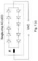
- FIG. 1( a )shows a schematic for an embodiment of a prior art AC-LED with which embodiments of the present invention might be used.
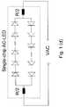
- FIGS. 1( b ), ( c ) and ( d )show embodiments of the present invention used with monolithically integrated “lump” current-limiting resistors.
- FIG. 1( e )shows an embodiment of the current invention used with monolithically integrated “distributed” current-limiting resistors.
- FIG. 2Cross-section view of an LED wafer material layer structure for one embodiment of the present invention.
- FIG. 3( a )shows a cross-section view of an embodiment of the present invention having a monolithically integrated resistor fabricated from doped n-GaN material in serial connection with the LED array through deposited wires on the chip.
- FIG. 3( b )shows a cross-section view of an embodiment comprising a monolithically integrated resistor which is fabricated from doped n-GaN material in series connection with an LED array through bumps which make electrical connection through wires disposed on a submount.
- FIG. 3( c )shows a cross-sectional view of an embodiment in which a monolithically integrated resistor fabricated from doped n-GaN material is oriented in serial connection with an LED array through n-GaN material.
- FIG. 3( d )shows cross-sectional view of an embodiment having a monolithically integrated resistor which is fabricated from doped n-GaN material and caused to be in serial connection with an LED array through bumps which make electrical contact through wires on a submount.
- FIG. 3( e )shows a top-view of an embodiment in which a “lump” resistor strip with compact zigzag geometry is utilized.
- FIG. 3( f )shows a top-view for an embodiment in which “distributed” resistors are linked with each individual mini-LED.
- FIG. 4shows a cross-section view of an embodiment using a monolithically integrated resistor fabricated from un-doped GaN material.
- FIG. 5shows a cross-section view of an embodiment including a monolithically integrated resistor fabricated from deposited thin-film material.
- FIG. 6shows an embodiment in which a current-limiting resistor is integrated with an AC/DC LED chip in a lamp package assembly.
- FIG. 7shows an embodiment where a current-limiting resistor chip is integrated with an AC/DC LED chip in a standard T1-3 ⁇ 4 lamp package and thus, is adapted to function as an indicator lamp.
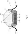
- FIG. 8shows an embodiment where a current-limiting resistor chip is integrated with AC/DC LED chip in a custom surface mounting package in order to function as a standard high-power AC lamp.
- FIG. 9shows an alternative embodiment in which the protection elements are integrated with AC/DC LED chip by incorporating them on the submount.
- the range for use for indicator lamp purposesis in the range of 0.5 by 0.5 to 0.2 by 0.2 millimeters.
- these chipsare about 0.4 by 0.4 millimeters for use in a T1-3 ⁇ 4 package
- the individual MicroLEDs used for these indicator-lamp types of applicationscan range in size from about 50 by 50 to 20 by 20 microns.
- the MicroLEDs usedare about 30 by 30 microns.
- Other types of packagesexist in which AC indicator LEDs can be used as well.
- the chip size and MicroLEDs sizewill vary based on the particular package arrangement selected and the number of MicroLEDs depends on the voltage requirement.
- AC power LEDsThe second other category of application is for illumination and lighting. But these applications require LEDs which provide more brightness and require higher power. (These LEDs are hereinafter referred to as an “AC power LEDs”).
- AC power LEDsIn commonly owned U.S. patent application Ser. No. 11/040,445 (the contents of which are hereby incorporated by reference), an AC power LED is heterogeneously integrated onto a submount, and the wire connections between the individual mini-LEDs are formed on the submount.
- SC power LEDsCommon owned U.S. patent application Ser. No. 11/040,445 (the contents of which are hereby incorporated by reference)
- AC power LEDis heterogeneously integrated onto a submount, and the wire connections between the individual mini-LEDs are formed on the submount.
- Ser. No. 11/144,982the contents of which are hereby incorporated by reference
- a plurality of AC power LED chipsare integrated onto one submount to form a large area AC/DC emitter to provide high power and brightness for lighting purposes
- the chip-size of AC power LEDis determined by the power level and line voltage. Since all the packages are custom-designed, there is no strict size limitation, correspondingly, the mini-LEDs used for these AC power LEDs are somewhat larger.
- the individual mini-LEDs used for these high-voltage applicationscan range in size from about 0.1 mm by 0.1 mm to 0.5 mm by 0.5 mm or even larger. In a preferred embodiment of a 1 W AC power LED arrangement has a chip size of about 1 mm by 1 mm. But one skilled in the art will recognize that the sizes for the mini-LEDs and chips will vary based on power design and voltage design. Therefore, specific sizes and mini-LEDs number should not be considered limiting unless specifically claimed.
- the high-voltage AC light emitterscan be directly powered by a standard 120 VAC power line (the most readily available power specifications in the United States and other locations) without the use of any voltage transformer. If the AC-LED is packaged with a standard Edison or European screw base, it can be directly screwed into the light bulb fixture, or plugged into the power outlet for lighting.
- a high voltage AC/DC LED arrangementwhich improves device reliability and durability by incorporating one or more current limitation and protection mechanisms.
- a protection elemente.g., a resistor
- the combined ACLED/protection element integrationis able to be packed in a package to form a completely included illuminator which is adequately protected from over voltage situations or current surges.
- protection elementsare resistors, it is possible that other devices or systems could be used instead which would provide the necessary protection against overvoltage and overcurrent situations. These alternative devices are also intended to be included within the meaning of “protection element” as used herein. Further, it is repeatedly discussed that the protection elements used are “integrated.”
- integrateddoes not mean that the protection element component is integral with any other component of the device unless otherwise specified. For example, in many instances the use of this term means the monolithic integration of protection elements and LED on the same chip, while in other instances the use of this term is intended to impart only that the overall device is able to function as a unified whole.
- the termmeans simply that the element is able to be easily packaged.
- This integrationenables ACLEDs to be included in conventional package arrangements and replace traditional incandescent and other lighting technologies as never before. No separate surge protection circuitry needs to be provided, because the protection here is integrated.
- the resistor and the ACLEDare fabricated on a same chip to form a monolithically integrated ACLED with protection.
- the resistoris built at the same time and using the same n-type semiconductor used in fabricating the ACLED. This can also be done using the p-type semiconductor material used to comprise the ACLED, an undoped semiconductor material in the ACLED, or even a combination of n-type, p-type, and undoped semiconductor materials during fabrication of the ACLED.
- III-nitride semiconductorse.g., GaAs, InP, AlGaAs, AlGaInP
- III-V semiconductorse.g., GaAs, InP, AlGaAs, AlGaInP
- II-VI semiconductorse.g., ZnO or SiC
- organic semiconductorse.g., organic semiconductors, or organic semiconductors.
- the resistorcould be constructed using externally-deposited materials other than those for LED, and the materials are deposited on LED chip.
- the materials used to construct the LED itselfseparately deposed tantalum nitride, nichrome, or other resistive materials could be used instead.
- the separately deposed resistive materialscan be serially connected with the LEDs using wires on the same chip.
- the resistor and ACLEDare serially connected through flip-chip bonding onto a submount.
- This embodimentcould take many forms, but in one, the resistor is built on the ACLED chip, and in the other, the resistor is built onto the submount and then serially connected using wires on the submount. Additionally, resistors, a positive temperature coefficient (“PTC”) thermistors, varistors, and capacitors, and or combinations could be electrically included into this type of arrangement.
- PTCpositive temperature coefficient
- the resistor and ACLEDare built on two separated chips and the integration is formed by wire bonding to connect the resistor with the ACLED somewhere in the package of illuminator.
- the resistance createdwill be more than 1K ohm for indicator LED running at a normal current less than about 1.5 mA. In preferred embodiments, however, the resistance provided should be in the range of from about 10 K ohms to 30 K ohms for indicator LED running at a normal current less than about 1.5 mA.
- the preferred resistance valuewill depend on the driving current. For example, for power AC-LEDs running at a normal 20 mA with the power grid voltage variation of 30V, the preferred resistance value will be about 1.5 K ohms. It is certainly possible that lower and/or higher resistance could be used and still fall within the scope of the present invention, however.
- the processes of the present inventionenable the user to create ACLED devices having a total size of less than about 0.5 mm by 0.5 mm. Devices this small are able to be packed in T1, T13 ⁇ 4 and other packages for low-power applications, and because of the integrated protection element(s) are able to function without falling victim to power variations existent in commercial power sources.
- a protection elemente.g., resistor
- a high-power lighting packageFor high-power lighting applications, for example, commercial lighting on 110V or 220V, these processes enable the user to create devices having total sizes of more than 0.5 mm by 0.5 mm. These arrangements usually use larger and more LEDs to generate more light, while consuming considerable power. Because of the processes disclosed herein, a protection element (e.g., resistor) is able to be easily incorporated within a high-power lighting package and provide desired performance without failing due to power fluctuations.
- FIG. 1( a )shows an AC-LED without any protection elements as disclosed in some earlier co-owned applications.
- FIGS. 1( b ), ( c ) and ( d )each illustrate the invention with different embodiments where the integrated protection elements are current-limiting resistors integrated on AC-LED chip. These resistors are fabricated at the same time as the AC-LED itself.
- a resistor (R)is in serial connection with the corresponding LED string.
- the resistor usedis what is commonly referred to as a current-limiting resistor.
- one current limiting resistor (R)is connected with the two current paths.
- FIG. 1( c )one current limiting resistor (R) is connected with the two current paths.
- LEDs shown in all the above, and hereinafter embodimentsmight be fabricated such that they emit white, blue, green, yellow, red, and other visible light. And the arrays created could be color homogenous, or mixed. Further, the LEDs could be adapted such that they emit infrared or ultraviolet wavelengths and still reap the benefits of the claimed invention. Thus, a particular emission-type of LED is not restrictive of the technological advances disclosed.
- the designed power consumptionis typically from 40 mW to 120 mW, with a maximum power consumption of about 150 mW, limited by the thermal dissipation capability of such package.
- the standard line voltageis 120 VAC
- the AC indicator LED lamp with a standard T1-3 ⁇ 4 packagehas the maximum current of about (or no more than) 1 mA. Since the current flowing through the LED exponentially increases with applied voltage, without any current limiting protection, when AC voltage drifting to 130V, the current flowing through the 120V rated AC-LED lamp will be significantly increased, and the input power will be several times higher than the maximum limitation; the AC-LED lamp will be destroyed in a very short time by heating effect.
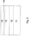
- the waferincludes an insulating substrate (such as sapphire), or an insulating layer deposited on a conducting substrate (such as Si, SiC or other substrate material) ( 11 ), an un-doped GaN layer ( 12 ), a Si-doped n-type GaN layer ( 13 ), a multi-quantum-well optical active region ( 14 ), and p-type GaN layer ( 15 ). Because of the intrinsic properties of the materials, the un-doped GaN layer 12 has n-type conductivity, but its conductivity is much lower than that of the intentionally doped GaN layer 13 .
- a conducting substratesuch as Si, SiC or other substrate material
- layer 12has a resistance of 0.1 to 1 ⁇ cm
- layer 13has a resistance of 0.003 to 0.03 ⁇ cm.
- the combination of layers 12 and 13is generally referred to as an n-GaN layer. It is well known that when GaN is grown on a substrate, a very thin amorphous layer with ⁇ 25 nm is first grown at low temperature ( ⁇ 550° C.), then annealed at high temperature (> ⁇ 950° C.) to form polycrystal as nucleation layer, following is the growth at high temperature of a thick GaN layer (> ⁇ 2 ⁇ m) as the buffer, so that the defects can be gradually reduced as the film becomes thick and single crystal is formed.
- the crystal thin-film epi-layers of the LED structureincluding n-type layer, multi-quantum-well optical active layers, and p-type layer can be gown with high crystal quality.
- the amorphous/polycrystal nucleation layer and buffer layeras undoped GaN layer ( 12 ).
- the doped n-type semiconductor material of LEDis used to fabricate the resistor with a designed resistance value.
- the waferis first etched to n-GaN layer 13 to expose doped n-GaN, and then etched to insulating substrate 11 to isolate each individual LED.
- Current spreading layer 20 , p-contact 19 , and n-contact 18are formed by metal deposition.
- an insulation material 16is deposed on the etched sidewall, and then metal line 17 is formed to serially connect individual mini-LEDs (micro-LEDs) to form one AC-LED.
- n-GaN strip with certain geometryis formed. After two n-contacts 18 deposited on the two ends of GaN strip, one end is connected with power input, and the other end is connected with the p-contact of first individual mini-LED (micro-LED) of AC-LED, a lump current-limiting resistor (R) is then integrated into the LED array. Electrical potential is made available using a first electrical electrode 31 and a second electrode 32 in a manner known to those skilled in the art. The lump resistor value depends on the fabricated doped n-GaN strip geometry and its resistivity.
- the resistor valueshould be adapted to meet requirements.
- the resistance necessarycan be created by controlling the geometries of the strip created according to the formula:
- Ris the resistance
- ⁇is the resistivity of the particular material used
- Ais the cross sectional area of the strip deposed
- Lis the length of the strip.
- AW ⁇ H, where W and H are the cross sectional width and height of the strip; thus, it may be seen that by manipulating strip cross sectional area (or width and height) and length in a manner most convenient to the particular device, the resistor is able to be monolithically incorporated into the device in a variety of ways.
- doped n-GaNwhich has a typical resistivity of 0.01 ⁇ cm, is geometrically deposed to achieve a resistor of 10 k ⁇ .
- the ratio of strip length over widthwill be 100:1. If the strip has a width of 5 ⁇ m, its length will be 500 ⁇ m.
- This stripmay be a straight one, or it may have a complex shape, such as zigzag shape, so the strip can be limited in a compact region.
- doped n-GaNis disclosed as the preferred semiconductor material used in FIG. 3( c ), it is also possible that other materials could be used instead or in addition.
- the semiconductor materials usedmight include crystalline and/or amorphous structures.
- III-nitride semiconductor GaNthe semiconductor might comprise different III-nitride semiconductors such as InN, AlN, and their alloys AlGaN, InGaN, AlGaInN, among others.
- III-V semiconductorsincluding GaAs, InP, AlGaAs, AlGaInP, or others might be used instead.
- semiconductor materials that are not III-nitride or III-V semiconductorscould be used, including ZnO, SiC, and others.
- These semiconductor materialsmight be organic semiconductors and/or organic electroluminescent materials. Further, they might be polymer electroluminescent materials. It should be understood that in this, and all of the other like embodiments disclosed, the particular materials used should not be considered as limiting unless specifically claimed.
- FIG. 3( b )an alternative environment for incorporation of the FIG. 3( a ) LED is disclosed. Support for this type of flip-chip arrangement can be found in commonly owned U.S. patent application Ser. No. 11/040,445, which has already been herein incorporated by reference.
- the '445 applicationdiscloses an AC power LED which was heterogeneously integrated on a submount, and the wire connections between the individual mini-LEDs were formed on that submount.
- FIG. 3( b )shows the addition of a lump resistor R constructed from n-GaN is also connected with the power terminal and a neighboring individual LED through bumps 54 and wires 53 on a submount.
- the submounthas a metal base 51 covered with an insulation material 52 .
- the submountcould take many forms depending on the circumstances.
- submountcould comprise polymer covered aluminum or copper.
- the submountcould be based on Silicon, SiC, AlN, or other materials.
- the FIG. 3( c ) LED fabricationincludes a substrate 111 , an undoped GaN layer 112 , an n-type GaN layer 113 , an active region 114 , a p-type GaN layer 115 , insulation material 116 , a metal line 117 , an n-contact 118 , a p-contact 119 , a current spreading layer 120 , and electrodes 131 and 132 .
- resistor R and its neighboring individual LEDare directly linked by doped n-GaN layer 113 .
- protection mechanism Ris integral with an extension of layer 113 . Because of this, there is no need for a separate metal connection wire because the resistor R is also directly linked with the power terminal through n-GaN material 113 .
- the materials usedshould not be considered a limitation unless specifically claimed. Although a doped n-GaN layer has been used herein, other materials like those described regarding the last embodiment could be used here as well and still fall within the broad concepts of the present invention.
- FIG. 3( d )A flip-chip bonded version is illustrated in FIG. 3( d ).
- the lump resistor R(comprised of extended n-type GaN layer 113 ) and each of the individual mini-LEDs are electrically connected with the power terminal and a neighboring individual mini-LED through bumps 154 and wires 153 on a submount.
- the submountin the preferred embodiment, has a metal base 151 covered with insulation material 152 . But as discussed already above, other submount arrangements are possible.
- FIG. 3( e )is the top-view of FIG. 3( c ), showing that the extended n-GaN layer 113 has been etched to have a zigzag shape.
- This zigzag shapeincreases the electrical travel distance through the n-GaN material 113 . Because of this, the shape increases the resistance between contact 132 and current-spreading layer 120 to the desired level.
- the shape of layer 113could be alternatively etched into any number of shapes; e.g., serpentine, straight; depending on the resistivity and other electrical specifications desired.
- FIG. 3( f )illustrates another example to incorporate current-limiting resistors by constructing distributed resistors (r) instead of a lump resistor (R).
- the FIG. 3( e ) embodimentlike with earlier examples, includes a fabrication including a substrate 311 , an undoped GaN layer, an n-type GaN layer 313 , an active region, a p-type GaN layer, insulation material 316 , a metal line 317 , an n-contact 318 , a p-contact 319 , a current spreading layer 320 , and electrodes 331 and 332 .
- FIG. 3( e )includes a fabrication including a substrate 311 , an undoped GaN layer, an n-type GaN layer 313 , an active region, a p-type GaN layer, insulation material 316 , a metal line 317 , an n-contact 318 , a p-contact 319 , a current spreading layer 320 , and
- each individual mini-LED of the AC-LEDhas a linked small resistor r which is comprised of n-type GaN 313 , and the resistance offered by the sum of all these small resistors is adapted to equal the desired level of resistance.
- the sum of the individual distributed resistorscould be configured to equal the resistance of lump resistor R (see FIG. 3( e )).
- the doped p-type semiconductor material of the LEDis used to fabricate the monolithic resistor
- p-type GaN strip 115is defined with a certain geometry (length and width) during the first etching step (when it is etched down to the n-GaN layer).
- the two p-GaN contactsare formed at two ends of p-GaN strip, and the sidewalls are also isolated with insulation material. See, e.g., insulation material 416 in FIG. 4 . With one end connecting with power input, and the other end connecting with the first individual LED, a current-limiting resistor is integrated into the LED array.
- the resistor valuedepends on the fabricated p-GaN geometry and its resistivity.
- p-GaNhas a typical resistivity of 2 ⁇ cm, and a thickness of 0.25 ⁇ m.
- the ratio of strip length over widthwill be 1:8.
- the doped p-type semiconductor materialwhich is above n-type semiconductor, is used to fabricate the resistor; the voltage on the resistor has a limitation, determined by semiconductor p-n junction breakdown voltage.
- the doped p-type materialse.g., layer 115
- the doped p-type materialscould also be extended to create the resistance necessary.
- the un-doped semiconductor material of LEDis used to fabricate the monolithic resistor.
- the deviceincludes a substrate 411 , an undoped GaN layer 412 , an n-type GaN layer 413 , an active region 414 , a p-type GaN layer 415 , insulation material 416 , a metal line 417 , an n-contact 418 , a p-contact 419 , a current spreading layer 420 , and electrodes 431 and 432 .
- One more etching stepis necessary for resistor fabrication. That step is to etch un-doped GaN layer 412 as disclosed in the figure.
- the resistoris connected in serial into the mini-LED strings (see FIG. 4 ).
- the resistor valuedepends on the fabricated un-doped GaN strip geometry and its resistivity.
- un-doped GaNhas a typical resistivity of 0.5 ⁇ cm, and a thickness of 1 ⁇ m.
- the ratio of strip length over widthwill be 1:2.
- Other geometric manipulationscould be used as well and still fall within the scope of the present invention.
- the FIG. 5 embodimentincludes a substrate 511 , an undoped GaN layer 512 , an n-type GaN layer 513 , an active region 514 , a p-type GaN layer 515 , insulation material 516 , a metal line 517 , an n-contact 518 , a p-contact 519 , a current spreading layer 520 , and electrodes 531 and 532 .
- This embodimentincludes a separately deposited current-limiting resistor 525 which is formed from deposited materials. These materials are deposited after etching down to the insulating substrate.
- a thin-film of certain materialspreferably tantalum nitride (TaN x ) or nichrome, is deposited with tens to hundreds of nanometers thickness and patterned into certain geometry to achieve the required resistance.
- TaN xtantalum nitride
- nichromenichrome
- the sheet resistance of TaN, or nichromeis in the range of 5 ⁇ /square to 250 ⁇ /square, which can meet the requirements of current-limiting resistor.
- the resistive materialis typically thermally annealed for oxidation to stabilize the resistance. It should be noted that the resistive materials could also be deposited on an insulating layer which has been deposited on a conducting substrate.
- a discrete bare-chip resistor 604is integrated with AC-LED chip 602 and included in a lamp package 600 , as shown in FIG. 6 .
- the lamp packagemay be a T1, T1-3 ⁇ 4, or other standard or custom LED packaging arrangement, including surface mounting kinds of packages.
- the packaged AC-LEDscan be configured to require low power for indication applications and high power for general lighting.
- FIG. 7shows an example of these general principles applied to a standard T1-3 ⁇ 4 package which can be used for indication applications.
- a lamp package 700is adapted to include a discrete bare-chip resistor 704 which is electrically connected with an AC-LED chip 702 using bonding wires 712 .
- standard package 700also includes an epoxy dome lens 706 , leads 708 , and a reflector cup 710 .
- Bare chip resistor 704is provided with a suitable resistance to protect the AC-LED chip 702 from damage.
- itis shown seated on one lead of the package frame by silver paste or other solders.
- the chip resistoris electrically connected with this lead through its bottom contact.
- the AC-LED chipis seated in reflection cup 710 .
- one electrode of the AC-LEDis bonded to the other lead of the package frame, and the other electrode of AC-LED is bonded to the top contact of the chip resistor 704 .
- the resistoris made to be in a series connection with the AC-LED chip 702 .
- Bare chip resistor 704has a preferred dimension of about 20 mil by 20 mil or even smaller, for example, the thin film back-contact resistor (BCR) from the company of Vishay Electro-Films has a size 20 by 20 mil. This sizing enables chip resistor 704 to easily fit into the compact package.
- FIG. 8shows another example in which the general principles are incorporated into a package arrangement 800 for an AC power LED chip 802 with a large chip size.
- Thisis normally a custom surface mounted package.
- a bare chip resistor 804 having suitable resistanceis seated on one of the leads 808 of the package frame by silver paste or other solders, and electrically connected with this lead through its bottom contact.
- the AC-LED chip 802is seated on a bottom metal slug 814 through a paste or solder 816 and included between insulation walls 810 and immersed in an encapsulate 806 .
- one electrode of the AC-LEDis bonded to the other lead of the package frame, and the other electrode of AC-LED is bonded to the top contact of chip resistor 804 , so that the resistor is in series connection with AC-LED chip.
- an AC-LED chip used in the FIG. 8 arrangementcould also be a bare chip, and could also be a flip-chip bonded assembly including an AC-LED chip and submount.
- an AC-LED chip 906is flip-chip mounted on a submount 902 (see the description for FIG. 3( b ) which discusses how this can be done), and the protection circuits and elements are then integrated onto that same submount 902 .
- This arrangementenables the incorporation of more complex protection.
- a varistor 908can be integrated on the submount such that it is connected across the AC power input.
- MOVmetal oxide varistors
- other devicescould also be incorporated to accomplish the same objectives and still fall within the scope of the present invention.
- 904is a tiny surface mounted resistor which is directly mounted on the submount, this device could be replaced with a positive temperature coefficient (PTC) thermistor.
- PTCpositive temperature coefficient
- the PTC thermistor 904is in a low resistance state.
- elevated temperaturescause PTC thermistor 904 to switch into a high resistance state thereby limiting the current flow through the LED to a normal operating level.
- the PTC thermistorresets to its low resistance state and permitting a normal operating current to flow through the LED device.
- silicon integrated circuit (IC) bare chipswhich can be used to stabilize the voltage or limit the current can also be integrated on the submount to protect LED device.
- protection device arrangements disclosed abovewould also be useful for protection of AC/DC LEDs which are connected into a circuit board arrangement.
Landscapes
- Led Devices (AREA)
- Led Device Packages (AREA)
Abstract
Description
Claims (18)
Priority Applications (3)
| Application Number | Priority Date | Filing Date | Title |
|---|---|---|---|
| US11/683,293US7714348B2 (en) | 2006-10-06 | 2007-03-07 | AC/DC light emitting diodes with integrated protection mechanism |
| PCT/US2007/070213WO2008045592A2 (en) | 2006-10-06 | 2007-06-01 | Ac/dc light emitting diodes with integrated protection mechanism |
| EP07798009AEP2080236A4 (en) | 2006-10-06 | 2007-06-01 | AC / DC LIGHT EMITTING DIODES WITH INTEGRATED PROTECTION MECHANISM |
Applications Claiming Priority (2)
| Application Number | Priority Date | Filing Date | Title |
|---|---|---|---|
| US85013506P | 2006-10-06 | 2006-10-06 | |
| US11/683,293US7714348B2 (en) | 2006-10-06 | 2007-03-07 | AC/DC light emitting diodes with integrated protection mechanism |
Publications (2)
| Publication Number | Publication Date |
|---|---|
| US20080083929A1 US20080083929A1 (en) | 2008-04-10 |
| US7714348B2true US7714348B2 (en) | 2010-05-11 |
Family
ID=39274357
Family Applications (1)
| Application Number | Title | Priority Date | Filing Date |
|---|---|---|---|
| US11/683,293ActiveUS7714348B2 (en) | 2006-10-06 | 2007-03-07 | AC/DC light emitting diodes with integrated protection mechanism |
Country Status (3)
| Country | Link |
|---|---|
| US (1) | US7714348B2 (en) |
| EP (1) | EP2080236A4 (en) |
| WO (1) | WO2008045592A2 (en) |
Cited By (21)
| Publication number | Priority date | Publication date | Assignee | Title |
|---|---|---|---|---|
| US20080173884A1 (en)* | 2007-01-22 | 2008-07-24 | Cree, Inc. | Wafer level phosphor coating method and devices fabricated utilizing method |
| US20080217628A1 (en)* | 2007-03-05 | 2008-09-11 | Seoul Semiconductor Co., Ltd. | Light emitting device |
| US20090065790A1 (en)* | 2007-01-22 | 2009-03-12 | Cree, Inc. | LED chips having fluorescent substrates with microholes and methods for fabricating |
| US20090189534A1 (en)* | 2008-01-30 | 2009-07-30 | Chien-Lung Wang | LED Lamp And Driving Apparatus For The Same |
| US20100102336A1 (en)* | 2008-10-29 | 2010-04-29 | Seoul Opto Device Co., Ltd. | Light emitting diode for ac operation |
| US20100225233A1 (en)* | 2009-03-05 | 2010-09-09 | Forward Electronics Co., Ltd. | Alternating current light emitting diode device |
| US20100289416A1 (en)* | 2006-08-18 | 2010-11-18 | Wen-Yung Yeh | Lighting devices |
| US20100295087A1 (en)* | 2007-01-16 | 2010-11-25 | Korea Photonics Technology Institute | Light Emitting Diode with High Electrostatic Discharge and Fabrication Method Thereof |
| US20110227490A1 (en)* | 2010-03-19 | 2011-09-22 | Active-Semi, Inc. | AC LED lamp involving an LED string having separately shortable sections |
| US20120112337A1 (en)* | 2008-09-04 | 2012-05-10 | Osram Opto Semiconductors Gmbh | Optoelectronic Component, and Method for the Production of an Optoelectronic Component |
| US20130020952A1 (en)* | 2011-07-20 | 2013-01-24 | Yu Pin Liao | AC Direct Drive Organic Light Emitting Diode Assembly |
| US8530909B2 (en) | 2010-12-27 | 2013-09-10 | Micron Technology, Inc. | Array assemblies with high voltage solid state lighting dies |
| US8809897B2 (en) | 2011-08-31 | 2014-08-19 | Micron Technology, Inc. | Solid state transducer devices, including devices having integrated electrostatic discharge protection, and associated systems and methods |
| US20140299908A1 (en)* | 2012-02-21 | 2014-10-09 | Peiching Ling | Light emitting diode package and method of fabricating the same |
| US20150097482A1 (en)* | 2012-03-08 | 2015-04-09 | Koninklijke Philips N.V. | Segmented electroluminescent device with distributed load elements |
| US20150179898A1 (en)* | 2011-02-16 | 2015-06-25 | Rohm Co., Ltd. | Led module |
| US9159888B2 (en) | 2007-01-22 | 2015-10-13 | Cree, Inc. | Wafer level phosphor coating method and devices fabricated utilizing method |
| US9490239B2 (en) | 2011-08-31 | 2016-11-08 | Micron Technology, Inc. | Solid state transducers with state detection, and associated systems and methods |
| US9543490B2 (en) | 2010-09-24 | 2017-01-10 | Seoul Semiconductor Co., Ltd. | Wafer-level light emitting diode package and method of fabricating the same |
| US10580929B2 (en) | 2016-03-30 | 2020-03-03 | Seoul Viosys Co., Ltd. | UV light emitting diode package and light emitting diode module having the same |
| US11205677B2 (en)* | 2017-01-24 | 2021-12-21 | Goertek, Inc. | Micro-LED device, display apparatus and method for manufacturing a micro-LED device |
Families Citing this family (104)
| Publication number | Priority date | Publication date | Assignee | Title |
|---|---|---|---|---|
| US20080149951A1 (en)* | 2006-12-22 | 2008-06-26 | Industrial Technology Research Institute | Light emitting device |
| TWI440210B (en) | 2007-01-22 | 2014-06-01 | Cree Inc | Illumination device using external interconnection array of light-emitting device and manufacturing method thereof |
| EP2111640B1 (en)* | 2007-01-22 | 2019-05-08 | Cree, Inc. | Fault tolerant light emitter and method of fabricating the same |
| KR100818466B1 (en)* | 2007-02-13 | 2008-04-02 | 삼성전기주식회사 | Semiconductor light emitting device |
| KR100974923B1 (en)* | 2007-03-19 | 2010-08-10 | 서울옵토디바이스주식회사 | Light emitting diode |
| KR100889956B1 (en)* | 2007-09-27 | 2009-03-20 | 서울옵토디바이스주식회사 | AC Light Emitting Diode |
| MX2010003769A (en)* | 2007-10-06 | 2010-09-10 | Lynk Labs Inc | Led circuits and assemblies. |
| DE102008024481B4 (en)* | 2008-05-21 | 2021-04-15 | Tdk Electronics Ag | Electrical component assembly |
| US20090301388A1 (en)* | 2008-06-05 | 2009-12-10 | Soraa Inc. | Capsule for high pressure processing and method of use for supercritical fluids |
| US9157167B1 (en) | 2008-06-05 | 2015-10-13 | Soraa, Inc. | High pressure apparatus and method for nitride crystal growth |
| US8871024B2 (en)* | 2008-06-05 | 2014-10-28 | Soraa, Inc. | High pressure apparatus and method for nitride crystal growth |
| US8097081B2 (en) | 2008-06-05 | 2012-01-17 | Soraa, Inc. | High pressure apparatus and method for nitride crystal growth |
| WO2010012299A1 (en)* | 2008-07-30 | 2010-02-04 | Osram Gesellschaft mit beschränkter Haftung | Circuit configuration having light-emitting diodes and arrangement of a substrate having light-emitting diodes |
| US8430958B2 (en)* | 2008-08-07 | 2013-04-30 | Soraa, Inc. | Apparatus and method for seed crystal utilization in large-scale manufacturing of gallium nitride |
| US10036099B2 (en) | 2008-08-07 | 2018-07-31 | Slt Technologies, Inc. | Process for large-scale ammonothermal manufacturing of gallium nitride boules |
| US8979999B2 (en) | 2008-08-07 | 2015-03-17 | Soraa, Inc. | Process for large-scale ammonothermal manufacturing of gallium nitride boules |
| US8021481B2 (en) | 2008-08-07 | 2011-09-20 | Soraa, Inc. | Process and apparatus for large-scale manufacturing of bulk monocrystalline gallium-containing nitride |
| US7939839B2 (en)* | 2008-09-11 | 2011-05-10 | Bridgelux, Inc. | Series connected segmented LED |
| US7976630B2 (en) | 2008-09-11 | 2011-07-12 | Soraa, Inc. | Large-area seed for ammonothermal growth of bulk gallium nitride and method of manufacture |
| US8354679B1 (en) | 2008-10-02 | 2013-01-15 | Soraa, Inc. | Microcavity light emitting diode method of manufacture |
| US20100295088A1 (en)* | 2008-10-02 | 2010-11-25 | Soraa, Inc. | Textured-surface light emitting diode and method of manufacture |
| US8455894B1 (en) | 2008-10-17 | 2013-06-04 | Soraa, Inc. | Photonic-crystal light emitting diode and method of manufacture |
| KR100999689B1 (en)* | 2008-10-17 | 2010-12-08 | 엘지이노텍 주식회사 | Semiconductor light emitting device and manufacturing method thereof, light emitting device having same |
| US20100109553A1 (en)* | 2008-11-05 | 2010-05-06 | Chu-Cheng Chang | Led bulb with zener diode, zener diode assembly or resistor connected in series |
| US9543392B1 (en) | 2008-12-12 | 2017-01-10 | Soraa, Inc. | Transparent group III metal nitride and method of manufacture |
| US8987156B2 (en) | 2008-12-12 | 2015-03-24 | Soraa, Inc. | Polycrystalline group III metal nitride with getter and method of making |
| US8878230B2 (en)* | 2010-03-11 | 2014-11-04 | Soraa, Inc. | Semi-insulating group III metal nitride and method of manufacture |
| USRE47114E1 (en) | 2008-12-12 | 2018-11-06 | Slt Technologies, Inc. | Polycrystalline group III metal nitride with getter and method of making |
| US8461071B2 (en)* | 2008-12-12 | 2013-06-11 | Soraa, Inc. | Polycrystalline group III metal nitride with getter and method of making |
| KR20100076083A (en)* | 2008-12-17 | 2010-07-06 | 서울반도체 주식회사 | Light emitting diode having plurality of light emitting cells and method of fabricating the same |
| DE102008064310B3 (en)* | 2008-12-20 | 2010-05-20 | Insta Elektro Gmbh | Circuit arrangement for operating high-voltage LED arrangement, has four standard resistors that are attached to temperature variable resistor in series switched manner, where standard resistors surround temperature variable resistor |
| KR101041436B1 (en) | 2009-01-09 | 2011-06-15 | 한국광기술원 | Vertical light emitting device including ESD protection function and manufacturing method thereof |
| US20110100291A1 (en)* | 2009-01-29 | 2011-05-05 | Soraa, Inc. | Plant and method for large-scale ammonothermal manufacturing of gallium nitride boules |
| US8247886B1 (en) | 2009-03-09 | 2012-08-21 | Soraa, Inc. | Polarization direction of optical devices using selected spatial configurations |
| TWM374153U (en)* | 2009-03-19 | 2010-02-11 | Intematix Technology Ct Corp | Light emitting device applied to AC drive |
| WO2010115294A1 (en)* | 2009-04-07 | 2010-10-14 | 海立尔股份有限公司 | Ac led structure with overload protection |
| US8299473B1 (en) | 2009-04-07 | 2012-10-30 | Soraa, Inc. | Polarized white light devices using non-polar or semipolar gallium containing materials and transparent phosphors |
| US8791499B1 (en) | 2009-05-27 | 2014-07-29 | Soraa, Inc. | GaN containing optical devices and method with ESD stability |
| DE102009036621B4 (en) | 2009-08-07 | 2023-12-21 | OSRAM Opto Semiconductors Gesellschaft mit beschränkter Haftung | Optoelectronic semiconductor component |
| DE102009037186A1 (en)* | 2009-08-12 | 2011-02-17 | Osram Opto Semiconductors Gmbh | Radiation-emitting semiconductor component |
| US9000466B1 (en) | 2010-08-23 | 2015-04-07 | Soraa, Inc. | Methods and devices for light extraction from a group III-nitride volumetric LED using surface and sidewall roughening |
| US9583678B2 (en) | 2009-09-18 | 2017-02-28 | Soraa, Inc. | High-performance LED fabrication |
| CN102630349B (en) | 2009-09-18 | 2017-06-13 | 天空公司 | Power light emitting diode and method of operating with current density |
| US9293644B2 (en) | 2009-09-18 | 2016-03-22 | Soraa, Inc. | Power light emitting diode and method with uniform current density operation |
| US8933644B2 (en) | 2009-09-18 | 2015-01-13 | Soraa, Inc. | LED lamps with improved quality of light |
| US8435347B2 (en) | 2009-09-29 | 2013-05-07 | Soraa, Inc. | High pressure apparatus with stackable rings |
| US9175418B2 (en) | 2009-10-09 | 2015-11-03 | Soraa, Inc. | Method for synthesis of high quality large area bulk gallium based crystals |
| US8905588B2 (en) | 2010-02-03 | 2014-12-09 | Sorra, Inc. | System and method for providing color light sources in proximity to predetermined wavelength conversion structures |
| US8740413B1 (en) | 2010-02-03 | 2014-06-03 | Soraa, Inc. | System and method for providing color light sources in proximity to predetermined wavelength conversion structures |
| US20110186874A1 (en)* | 2010-02-03 | 2011-08-04 | Soraa, Inc. | White Light Apparatus and Method |
| US10147850B1 (en) | 2010-02-03 | 2018-12-04 | Soraa, Inc. | System and method for providing color light sources in proximity to predetermined wavelength conversion structures |
| DE102010008603A1 (en)* | 2010-02-19 | 2011-08-25 | OSRAM Opto Semiconductors GmbH, 93055 | Electrical resistance element |
| JP2011249411A (en)* | 2010-05-24 | 2011-12-08 | Seiwa Electric Mfg Co Ltd | Semiconductor light-emitting element, light-emitting device, illumination device, display device, signal light unit and road information device |
| US9450143B2 (en) | 2010-06-18 | 2016-09-20 | Soraa, Inc. | Gallium and nitrogen containing triangular or diamond-shaped configuration for optical devices |
| US9564320B2 (en) | 2010-06-18 | 2017-02-07 | Soraa, Inc. | Large area nitride crystal and method for making it |
| US20120007102A1 (en)* | 2010-07-08 | 2012-01-12 | Soraa, Inc. | High Voltage Device and Method for Optical Devices |
| US9913338B2 (en) | 2010-07-28 | 2018-03-06 | Epistar Corporation | Light-emitting device with temperature compensation |
| US9548286B2 (en) | 2010-08-09 | 2017-01-17 | Micron Technology, Inc. | Solid state lights with thermal control elements |
| JP2012049385A (en)* | 2010-08-27 | 2012-03-08 | Seiwa Electric Mfg Co Ltd | Semiconductor light-emitting element, light-emitting device, luminaire, display device and method of manufacturing semiconductor light-emitting element |
| NL2005418C2 (en) | 2010-09-29 | 2012-04-02 | Europ Intelligence B V | Intrinsically safe led display. |
| US8729559B2 (en) | 2010-10-13 | 2014-05-20 | Soraa, Inc. | Method of making bulk InGaN substrates and devices thereon |
| TWI472058B (en) | 2010-10-13 | 2015-02-01 | Interlight Optotech Corp | Light-emitting diode device |
| CN102032539B (en)* | 2010-10-28 | 2012-11-21 | 映瑞光电科技(上海)有限公司 | Lighting circuit |
| CN102563391A (en)* | 2010-12-22 | 2012-07-11 | 深圳市长运通光电技术有限公司 | Led light source |
| JP5776014B2 (en)* | 2011-05-17 | 2015-09-09 | パナソニックIpマネジメント株式会社 | Lighting device and lighting fixture |
| US8786053B2 (en) | 2011-01-24 | 2014-07-22 | Soraa, Inc. | Gallium-nitride-on-handle substrate materials and devices and method of manufacture |
| TWI535331B (en)* | 2011-01-31 | 2016-05-21 | Midas Wei Trading Co Ltd | Light emitting diode protection circuit |
| US9035337B2 (en)* | 2011-02-14 | 2015-05-19 | Semiconductor Energy Laboratory Co., Ltd. | Light-emitting module, light-emitting panel, and lighting device |
| JP2012174508A (en)* | 2011-02-22 | 2012-09-10 | Panasonic Corp | Lighting apparatus |
| CN103548162B (en)* | 2011-05-24 | 2016-11-09 | 皇家飞利浦有限公司 | P-N Separation Metal Filler for Flip Chip LED |
| US8492185B1 (en) | 2011-07-14 | 2013-07-23 | Soraa, Inc. | Large area nonpolar or semipolar gallium and nitrogen containing substrate and resulting devices |
| US8686431B2 (en) | 2011-08-22 | 2014-04-01 | Soraa, Inc. | Gallium and nitrogen containing trilateral configuration for optical devices |
| DE102011114253A1 (en)* | 2011-09-26 | 2013-03-28 | e:lumix OptoSemi Industries Verwaltungs GmbH | Lighting device e.g. street light comprises resistive element with positive temperature characteristic that is electrically connected with semiconductor element in series through thermal coupling and electrical connection |
| US9694158B2 (en) | 2011-10-21 | 2017-07-04 | Ahmad Mohamad Slim | Torque for incrementally advancing a catheter during right heart catheterization |
| US10029955B1 (en) | 2011-10-24 | 2018-07-24 | Slt Technologies, Inc. | Capsule for high pressure, high temperature processing of materials and methods of use |
| DE102012101606B4 (en) | 2011-10-28 | 2024-11-21 | Tdk Electronics Ag | ESD protection component and component with an ESD protection component and an LED |
| US8912025B2 (en) | 2011-11-23 | 2014-12-16 | Soraa, Inc. | Method for manufacture of bright GaN LEDs using a selective removal process |
| US8482104B2 (en) | 2012-01-09 | 2013-07-09 | Soraa, Inc. | Method for growth of indium-containing nitride films |
| JP2015509669A (en) | 2012-03-06 | 2015-03-30 | ソラア インコーポレーテッドSoraa Inc. | Light emitting diode with low refractive index material layer to reduce guided light effect |
| JP2013197456A (en)* | 2012-03-22 | 2013-09-30 | Stanley Electric Co Ltd | Led array and vehicular lighting fixture |
| KR20130128841A (en) | 2012-05-18 | 2013-11-27 | 삼성전자주식회사 | Semiconductor light emitting device having a multi-cell array and manufacturing method for the same, light emitting module and illumination apparatus |
| DE102012104494A1 (en) | 2012-05-24 | 2013-11-28 | Epcos Ag | light emitting diode device |
| TWI488295B (en)* | 2012-05-25 | 2015-06-11 | Phostek Inc | Light-emitting diode array and method for manufacturing the same |
| TWI629777B (en)* | 2012-08-06 | 2018-07-11 | 晶元光電股份有限公司 | Light-emitting diode |
| TWI538184B (en) | 2012-08-06 | 2016-06-11 | 晶元光電股份有限公司 | Light-emitting diode array |
| TWI704687B (en)* | 2012-08-06 | 2020-09-11 | 晶元光電股份有限公司 | Light-emitting diode |
| TWI612653B (en)* | 2012-08-06 | 2018-01-21 | 晶元光電股份有限公司 | Light-emitting diode |
| US8971368B1 (en) | 2012-08-16 | 2015-03-03 | Soraa Laser Diode, Inc. | Laser devices having a gallium and nitrogen containing semipolar surface orientation |
| US9978904B2 (en) | 2012-10-16 | 2018-05-22 | Soraa, Inc. | Indium gallium nitride light emitting devices |
| US8802471B1 (en) | 2012-12-21 | 2014-08-12 | Soraa, Inc. | Contacts for an n-type gallium and nitrogen substrate for optical devices |
| US20140231852A1 (en)* | 2013-02-15 | 2014-08-21 | Seoul Viosys Co., Ltd. | Led chip resistant to electrostatic discharge and led package including the same |
| US9194569B2 (en)* | 2013-03-05 | 2015-11-24 | Interlight Optotech Corporation | Illuminant device with over-temperature protecting function |
| US8994033B2 (en) | 2013-07-09 | 2015-03-31 | Soraa, Inc. | Contacts for an n-type gallium and nitrogen substrate for optical devices |
| WO2015063951A1 (en)* | 2013-11-01 | 2015-05-07 | 星和電機株式会社 | Semiconductor light-emitting element and light-emitting device |
| US9419189B1 (en) | 2013-11-04 | 2016-08-16 | Soraa, Inc. | Small LED source with high brightness and high efficiency |
| JP6203147B2 (en)* | 2014-01-29 | 2017-09-27 | シャープ株式会社 | Light emitting device |
| US10159121B2 (en)* | 2015-07-02 | 2018-12-18 | Lumileds Holding B.V. | LED lighting device |
| US10223962B2 (en)* | 2016-03-21 | 2019-03-05 | X-Celeprint Limited | Display with fused LEDs |
| TWI646680B (en)* | 2017-01-10 | 2019-01-01 | 英屬開曼群島商錼創科技股份有限公司 | Miniature LED chip and display panel |
| US10174438B2 (en) | 2017-03-30 | 2019-01-08 | Slt Technologies, Inc. | Apparatus for high pressure reaction |
| CN109860364B (en)* | 2017-08-30 | 2020-09-01 | 天津三安光电有限公司 | Light emitting diode |
| US20220384688A1 (en)* | 2017-08-30 | 2022-12-01 | Xiamen San'an Optoelectronics Co., Ltd. | Micro light-emitting diode and micro light-emitting diode array |
| CN111108613B (en)* | 2017-09-13 | 2024-01-16 | 夏普株式会社 | LED unit, image display element and manufacturing method thereof |
| CN110224049A (en) | 2019-05-31 | 2019-09-10 | 深圳市华星光电半导体显示技术有限公司 | Micro LED chip and preparation method thereof |
Citations (44)
| Publication number | Priority date | Publication date | Assignee | Title |
|---|---|---|---|---|
| US5278432A (en) | 1992-08-27 | 1994-01-11 | Quantam Devices, Inc. | Apparatus for providing radiant energy |
| US5317170A (en) | 1990-11-29 | 1994-05-31 | Xerox Corporation | High density, independently addressable, surface emitting semiconductor laser/light emitting diode arrays without a substrate |
| US5463280A (en)* | 1994-03-03 | 1995-10-31 | National Service Industries, Inc. | Light emitting diode retrofit lamp |
| US5563422A (en) | 1993-04-28 | 1996-10-08 | Nichia Chemical Industries, Ltd. | Gallium nitride-based III-V group compound semiconductor device and method of producing the same |
| US5699073A (en) | 1996-03-04 | 1997-12-16 | Motorola | Integrated electro-optical package with carrier ring and method of fabrication |
| US5773130A (en) | 1996-06-06 | 1998-06-30 | Motorola, Inc. | Multi-color organic electroluminescent device |
| JPH11150303A (en)* | 1997-11-14 | 1999-06-02 | Sanyo Electric Co Ltd | Light emitting parts |
| US5929466A (en) | 1994-03-09 | 1999-07-27 | Kabushiki Kaisha Toshiba | Semiconductor device and method of fabricating the same |
| US5952680A (en) | 1994-10-11 | 1999-09-14 | International Business Machines Corporation | Monolithic array of light emitting diodes for the generation of light at multiple wavelengths and its use for multicolor display applications |
| US5955748A (en) | 1994-07-19 | 1999-09-21 | Oki Electric Industry Co., Ltd. | End face light emitting type light emitting diode |
| US5966393A (en) | 1996-12-13 | 1999-10-12 | The Regents Of The University Of California | Hybrid light-emitting sources for efficient and cost effective white lighting and for full-color applications |
| US6054724A (en) | 1996-10-09 | 2000-04-25 | Oki Electric Industry Co., Ltd. | Light-emitting diode, light-emitting diode array |
| US6198405B1 (en) | 1997-01-03 | 2001-03-06 | Telefonaktiebolaget Lm Ericsson | Driver circuit and method of operating the same |
| US20020006040A1 (en) | 1997-11-25 | 2002-01-17 | Kazuo Kamada | Led luminaire with light control means |
| US20020043943A1 (en) | 2000-10-10 | 2002-04-18 | Menzer Randy L. | LED array primary display light sources employing dynamically switchable bypass circuitry |
| US6410940B1 (en) | 2000-06-15 | 2002-06-25 | Kansas State University Research Foundation | Micro-size LED and detector arrays for minidisplay, hyper-bright light emitting diodes, lighting, and UV detector and imaging sensor applications |
| US6455878B1 (en) | 2001-05-15 | 2002-09-24 | Lumileds Lighting U.S., Llc | Semiconductor LED flip-chip having low refractive index underfill |
| US6461019B1 (en) | 1998-08-28 | 2002-10-08 | Fiber Optic Designs, Inc. | Preferred embodiment to LED light string |
| US6547249B2 (en) | 2001-03-29 | 2003-04-15 | Lumileds Lighting U.S., Llc | Monolithic series/parallel led arrays formed on highly resistive substrates |
| US6635902B1 (en) | 2002-05-24 | 2003-10-21 | Para Light Electronics Co., Ltd. | Serial connection structure of light emitting diode chip |
| US20040080941A1 (en) | 2002-10-24 | 2004-04-29 | Hongxing Jiang | Light emitting diodes for high AC voltage operation and general lighting |
| US6740960B1 (en) | 1997-10-31 | 2004-05-25 | Micron Technology, Inc. | Semiconductor package including flex circuit, interconnects and dense array external contacts |
| US20040129946A1 (en) | 2002-10-17 | 2004-07-08 | Hideo Nagai | Light emission apparatus |
| US20040206970A1 (en) | 2003-04-16 | 2004-10-21 | Martin Paul S. | Alternating current light emitting device |
| US20050127816A1 (en) | 2003-12-16 | 2005-06-16 | Naofumi Sumitani | Light emitting device and method of manufacturing the same |
| US20050133816A1 (en) | 2003-12-19 | 2005-06-23 | Zhaoyang Fan | III-nitride quantum-well field effect transistors |
| US20050161682A1 (en) | 2003-05-05 | 2005-07-28 | Joseph Mazzochette | Light emitting diodes packaged for high temperature operation |
| US6936855B1 (en) | 2002-01-16 | 2005-08-30 | Shane Harrah | Bendable high flux LED array |
| US20050251698A1 (en) | 2004-05-10 | 2005-11-10 | Manuel Lynch | Cuttable illuminated panel |
| US20050253151A1 (en) | 2002-08-29 | 2005-11-17 | Shiro Sakai | Light-emitting device having light-emitting elements |
| US20050254243A1 (en) | 2002-10-24 | 2005-11-17 | Hongxing Jiang | Light emitting diodes for high AC voltage operation and general lighting |
| US20060044864A1 (en) | 2004-08-31 | 2006-03-02 | Ming-Te Lin | Structure of AC light-emitting diode dies |
| US7045965B2 (en) | 2004-01-30 | 2006-05-16 | 1 Energy Solutions, Inc. | LED light module and series connected light modules |
| US20060138443A1 (en) | 2004-12-23 | 2006-06-29 | Iii-N Technology, Inc. | Encapsulation and packaging of ultraviolet and deep-ultraviolet light emitting diodes |
| US20060163589A1 (en) | 2005-01-21 | 2006-07-27 | Zhaoyang Fan | Heterogeneous integrated high voltage DC/AC light emitter |
| US20060169993A1 (en) | 2005-02-03 | 2006-08-03 | Zhaoyang Fan | Micro-LED based high voltage AC/DC indicator lamp |
| US20060175681A1 (en) | 2005-02-08 | 2006-08-10 | Jing Li | Method to grow III-nitride materials using no buffer layer |
| US20060181877A1 (en) | 2005-02-14 | 2006-08-17 | Sidwell Steven C | LED assembly with LED position template and method of making an LED assembly using LED position template |
| US20060180818A1 (en) | 2003-07-30 | 2006-08-17 | Hideo Nagai | Semiconductor light emitting device, light emitting module and lighting apparatus |
| US20060208264A1 (en) | 2004-03-18 | 2006-09-21 | Ryu Yung H | Nitride semiconductor LED improved in lighting efficiency and fabrication method thereof |
| US7148515B1 (en)* | 2006-01-07 | 2006-12-12 | Tyntek Corp. | Light emitting device having integrated rectifier circuit in substrate |
| US7154149B2 (en)* | 2003-07-31 | 2006-12-26 | Epistar Corporation | EDS protection configuration and method for light emitting diodes |
| US7285801B2 (en) | 2004-04-02 | 2007-10-23 | Lumination, Llc | LED with series-connected monolithically integrated mesas |
| US20070273299A1 (en)* | 2004-02-25 | 2007-11-29 | Michael Miskin | AC light emitting diode and AC LED drive methods and apparatus |
Family Cites Families (4)
| Publication number | Priority date | Publication date | Assignee | Title |
|---|---|---|---|---|
| DE19728763B4 (en)* | 1997-07-07 | 2007-10-31 | Reitter & Schefenacker Gmbh & Co. Kg | Circuit device for protecting current-driven light sources, in particular LEDs, for signaling or lighting purposes |
| US6936885B2 (en)* | 2000-01-17 | 2005-08-30 | Samsung Electronics Co., Ltd. | NAND-type flash memory devices and methods of fabricating the same |
| JP4697397B2 (en)* | 2005-02-16 | 2011-06-08 | サンケン電気株式会社 | Composite semiconductor device |
| US7528267B2 (en)* | 2005-08-01 | 2009-05-05 | Girindus America, Inc. | Method for enantioselective hydrogenation of chromenes |
- 2007
- 2007-03-07USUS11/683,293patent/US7714348B2/enactiveActive
- 2007-06-01EPEP07798009Apatent/EP2080236A4/ennot_activeCeased
- 2007-06-01WOPCT/US2007/070213patent/WO2008045592A2/enactiveApplication Filing
Patent Citations (50)
| Publication number | Priority date | Publication date | Assignee | Title |
|---|---|---|---|---|
| US5317170A (en) | 1990-11-29 | 1994-05-31 | Xerox Corporation | High density, independently addressable, surface emitting semiconductor laser/light emitting diode arrays without a substrate |
| US5278432A (en) | 1992-08-27 | 1994-01-11 | Quantam Devices, Inc. | Apparatus for providing radiant energy |
| US5563422A (en) | 1993-04-28 | 1996-10-08 | Nichia Chemical Industries, Ltd. | Gallium nitride-based III-V group compound semiconductor device and method of producing the same |
| US5652434A (en) | 1993-04-28 | 1997-07-29 | Nichia Chemical Industries, Ltd. | Gallium nitride-based III-V group compound semiconductor |
| US5767581A (en) | 1993-04-28 | 1998-06-16 | Nichia Chemical Industries, Ltd. | Gallium nitride-based III-V group compound semiconductor |
| US6093965A (en) | 1993-04-28 | 2000-07-25 | Nichia Chemical Industries Ltd. | Gallium nitride-based III-V group compound semiconductor |
| US5877558A (en) | 1993-04-28 | 1999-03-02 | Nichia Chemical Industries, Ltd. | Gallium nitride-based III-V group compound semiconductor |
| US5463280A (en)* | 1994-03-03 | 1995-10-31 | National Service Industries, Inc. | Light emitting diode retrofit lamp |
| US5929466A (en) | 1994-03-09 | 1999-07-27 | Kabushiki Kaisha Toshiba | Semiconductor device and method of fabricating the same |
| US5955748A (en) | 1994-07-19 | 1999-09-21 | Oki Electric Industry Co., Ltd. | End face light emitting type light emitting diode |
| US5952680A (en) | 1994-10-11 | 1999-09-14 | International Business Machines Corporation | Monolithic array of light emitting diodes for the generation of light at multiple wavelengths and its use for multicolor display applications |
| US5699073A (en) | 1996-03-04 | 1997-12-16 | Motorola | Integrated electro-optical package with carrier ring and method of fabrication |
| US5773130A (en) | 1996-06-06 | 1998-06-30 | Motorola, Inc. | Multi-color organic electroluminescent device |
| US6054724A (en) | 1996-10-09 | 2000-04-25 | Oki Electric Industry Co., Ltd. | Light-emitting diode, light-emitting diode array |
| US5966393A (en) | 1996-12-13 | 1999-10-12 | The Regents Of The University Of California | Hybrid light-emitting sources for efficient and cost effective white lighting and for full-color applications |
| US6198405B1 (en) | 1997-01-03 | 2001-03-06 | Telefonaktiebolaget Lm Ericsson | Driver circuit and method of operating the same |
| US6740960B1 (en) | 1997-10-31 | 2004-05-25 | Micron Technology, Inc. | Semiconductor package including flex circuit, interconnects and dense array external contacts |
| JPH11150303A (en)* | 1997-11-14 | 1999-06-02 | Sanyo Electric Co Ltd | Light emitting parts |
| US20020006040A1 (en) | 1997-11-25 | 2002-01-17 | Kazuo Kamada | Led luminaire with light control means |
| US6461019B1 (en) | 1998-08-28 | 2002-10-08 | Fiber Optic Designs, Inc. | Preferred embodiment to LED light string |
| US6410940B1 (en) | 2000-06-15 | 2002-06-25 | Kansas State University Research Foundation | Micro-size LED and detector arrays for minidisplay, hyper-bright light emitting diodes, lighting, and UV detector and imaging sensor applications |
| US20020043943A1 (en) | 2000-10-10 | 2002-04-18 | Menzer Randy L. | LED array primary display light sources employing dynamically switchable bypass circuitry |
| US6547249B2 (en) | 2001-03-29 | 2003-04-15 | Lumileds Lighting U.S., Llc | Monolithic series/parallel led arrays formed on highly resistive substrates |
| US6455878B1 (en) | 2001-05-15 | 2002-09-24 | Lumileds Lighting U.S., Llc | Semiconductor LED flip-chip having low refractive index underfill |
| US6936855B1 (en) | 2002-01-16 | 2005-08-30 | Shane Harrah | Bendable high flux LED array |
| US6635902B1 (en) | 2002-05-24 | 2003-10-21 | Para Light Electronics Co., Ltd. | Serial connection structure of light emitting diode chip |
| US20050253151A1 (en) | 2002-08-29 | 2005-11-17 | Shiro Sakai | Light-emitting device having light-emitting elements |
| US20040129946A1 (en) | 2002-10-17 | 2004-07-08 | Hideo Nagai | Light emission apparatus |
| US20050254243A1 (en) | 2002-10-24 | 2005-11-17 | Hongxing Jiang | Light emitting diodes for high AC voltage operation and general lighting |
| US20050185401A1 (en) | 2002-10-24 | 2005-08-25 | Iii-N Technology, Inc. | Light emitting diodes for high AC voltage operation and general lighting |
| US20040080941A1 (en) | 2002-10-24 | 2004-04-29 | Hongxing Jiang | Light emitting diodes for high AC voltage operation and general lighting |
| US6957899B2 (en) | 2002-10-24 | 2005-10-25 | Hongxing Jiang | Light emitting diodes for high AC voltage operation and general lighting |
| US20040206970A1 (en) | 2003-04-16 | 2004-10-21 | Martin Paul S. | Alternating current light emitting device |
| US20050161682A1 (en) | 2003-05-05 | 2005-07-28 | Joseph Mazzochette | Light emitting diodes packaged for high temperature operation |
| US20060180818A1 (en) | 2003-07-30 | 2006-08-17 | Hideo Nagai | Semiconductor light emitting device, light emitting module and lighting apparatus |
| US7154149B2 (en)* | 2003-07-31 | 2006-12-26 | Epistar Corporation | EDS protection configuration and method for light emitting diodes |
| US20050127816A1 (en) | 2003-12-16 | 2005-06-16 | Naofumi Sumitani | Light emitting device and method of manufacturing the same |
| US20050133816A1 (en) | 2003-12-19 | 2005-06-23 | Zhaoyang Fan | III-nitride quantum-well field effect transistors |
| US7045965B2 (en) | 2004-01-30 | 2006-05-16 | 1 Energy Solutions, Inc. | LED light module and series connected light modules |
| US20070273299A1 (en)* | 2004-02-25 | 2007-11-29 | Michael Miskin | AC light emitting diode and AC LED drive methods and apparatus |
| US20060208264A1 (en) | 2004-03-18 | 2006-09-21 | Ryu Yung H | Nitride semiconductor LED improved in lighting efficiency and fabrication method thereof |
| US7285801B2 (en) | 2004-04-02 | 2007-10-23 | Lumination, Llc | LED with series-connected monolithically integrated mesas |
| US20050251698A1 (en) | 2004-05-10 | 2005-11-10 | Manuel Lynch | Cuttable illuminated panel |
| US20060044864A1 (en) | 2004-08-31 | 2006-03-02 | Ming-Te Lin | Structure of AC light-emitting diode dies |
| US20060138443A1 (en) | 2004-12-23 | 2006-06-29 | Iii-N Technology, Inc. | Encapsulation and packaging of ultraviolet and deep-ultraviolet light emitting diodes |
| US20060163589A1 (en) | 2005-01-21 | 2006-07-27 | Zhaoyang Fan | Heterogeneous integrated high voltage DC/AC light emitter |
| US20060169993A1 (en) | 2005-02-03 | 2006-08-03 | Zhaoyang Fan | Micro-LED based high voltage AC/DC indicator lamp |
| US20060175681A1 (en) | 2005-02-08 | 2006-08-10 | Jing Li | Method to grow III-nitride materials using no buffer layer |
| US20060181877A1 (en) | 2005-02-14 | 2006-08-17 | Sidwell Steven C | LED assembly with LED position template and method of making an LED assembly using LED position template |
| US7148515B1 (en)* | 2006-01-07 | 2006-12-12 | Tyntek Corp. | Light emitting device having integrated rectifier circuit in substrate |
Non-Patent Citations (11)
| Title |
|---|
| C. W Jeon, H.W. Choi and M.D. Dawson; A Novel Fabrication Method For A 64×64 Matrix-Addressable GaN-Based Micro-LED Array; Phys. Stat. Sol. (a) No. 1, 78-82, 2003. |
| Chen, Chang, Chen, Fann, Jiang, and Lin; Mechanism of Photoluminescence in GaN/Al (0.2)Ga(0.8)N Superlattices; Applied Physics Letters, vol. 79, No. 23; Dec. 3, 2001. |
| Dr. Jing Li; Ill-Nitride Integrated Photonic Devices (undated). |
| Jiang and Lin; Advances in iii-Nitride Micro-size light Emitters; Advanced Semiconductor Magazine; vol. 14, No. 5. |
| Jiang and Lin; On Display; OE Magazine Jul. 2001. |
| Kansas Researchers Fabricate Blue Micro Light-Emitting Diodes, Paving Way for Microdisplays, Energy Saving Lighting; Ascribe The Public Interest Newswire, Sep. 27, 2001. |
| Mair et al., Optical properties of GaN/AlGaN multiple quantum well microdisks, Nov. 17, 1997, Appl. Phys, Lett. 76 (5) p. 631, American Institute of Physics. |
| Preliminary Report on Patentability in related PCT Patent Application Serial No. PCT/US07/70213, issued Apr. 16, 2009, 8 pages. |
| S X Jin, J Li, J Y Lin and H X Jiang, InGaN/GaN Quantum Well Interconnected Microdisk Light Emitting Diodes; Applied Physics Letters, vol. 77, No. 20, p. 3236-3238, Nov. 13, 2000. |
| Zhaoyang Fan, Hongxing Jiang, Jingyu Lin; Related and Copending U.S. Appl. No. 11/144,982, filed Jun. 3, 2005. |
| Zhaoyang Fan; Related and Copending U.S. Appl. No. 11/340,296, filed Jan. 26, 2006. |
Cited By (50)
| Publication number | Priority date | Publication date | Assignee | Title |
|---|---|---|---|---|
| US20100289416A1 (en)* | 2006-08-18 | 2010-11-18 | Wen-Yung Yeh | Lighting devices |
| US8089218B2 (en)* | 2006-08-18 | 2012-01-03 | Industrial Technology Research Institute | Lighting devices |
| US20100295087A1 (en)* | 2007-01-16 | 2010-11-25 | Korea Photonics Technology Institute | Light Emitting Diode with High Electrostatic Discharge and Fabrication Method Thereof |
| US8294167B2 (en)* | 2007-01-16 | 2012-10-23 | Korea Photonics Technology Institute | Light emitting diode with high electrostatic discharge and fabrication method thereof |
| US20080173884A1 (en)* | 2007-01-22 | 2008-07-24 | Cree, Inc. | Wafer level phosphor coating method and devices fabricated utilizing method |
| US20090065790A1 (en)* | 2007-01-22 | 2009-03-12 | Cree, Inc. | LED chips having fluorescent substrates with microholes and methods for fabricating |
| US9196799B2 (en)* | 2007-01-22 | 2015-11-24 | Cree, Inc. | LED chips having fluorescent substrates with microholes and methods for fabricating |
| US9159888B2 (en) | 2007-01-22 | 2015-10-13 | Cree, Inc. | Wafer level phosphor coating method and devices fabricated utilizing method |
| US9024349B2 (en) | 2007-01-22 | 2015-05-05 | Cree, Inc. | Wafer level phosphor coating method and devices fabricated utilizing method |
| US20080217628A1 (en)* | 2007-03-05 | 2008-09-11 | Seoul Semiconductor Co., Ltd. | Light emitting device |
| US20090189534A1 (en)* | 2008-01-30 | 2009-07-30 | Chien-Lung Wang | LED Lamp And Driving Apparatus For The Same |
| US7888882B2 (en)* | 2008-01-30 | 2011-02-15 | Alliance Optotek Co., Ltd. | LED lamp and driving apparatus for the same |
| US20120112337A1 (en)* | 2008-09-04 | 2012-05-10 | Osram Opto Semiconductors Gmbh | Optoelectronic Component, and Method for the Production of an Optoelectronic Component |
| US8502252B2 (en)* | 2008-09-04 | 2013-08-06 | Osram Opto Semiconductor Gmbh | Optoelectronic component, and method for the production of an optoelectronic component |
| US8188489B2 (en)* | 2008-10-29 | 2012-05-29 | Seoul Opto Device Co., Ltd. | Light emitting diode for AC operation |
| US8232565B2 (en) | 2008-10-29 | 2012-07-31 | Seoul Opto Device Co., Ltd. | Light emitting diode for AC operation |
| US20100102336A1 (en)* | 2008-10-29 | 2010-04-29 | Seoul Opto Device Co., Ltd. | Light emitting diode for ac operation |
| US20100102337A1 (en)* | 2008-10-29 | 2010-04-29 | Seoul Opto Device Co., Ltd. | Light emitting diode for ac operation |
| US8373353B2 (en)* | 2009-03-05 | 2013-02-12 | Forward Electronics Co., Ltd. | Alternating current light emitting diode device |
| US20100225233A1 (en)* | 2009-03-05 | 2010-09-09 | Forward Electronics Co., Ltd. | Alternating current light emitting diode device |
| US20110227490A1 (en)* | 2010-03-19 | 2011-09-22 | Active-Semi, Inc. | AC LED lamp involving an LED string having separately shortable sections |
| US9544960B2 (en)* | 2010-03-19 | 2017-01-10 | Active-Semi, Inc. | AC LED lamp involving an LED string having separately shortable sections |
| US10892386B2 (en) | 2010-09-24 | 2021-01-12 | Seoul Semiconductor Co., Ltd. | Wafer-level light emitting diode package and method of fabricating the same |
| US10069048B2 (en) | 2010-09-24 | 2018-09-04 | Seoul Viosys Co., Ltd. | Wafer-level light emitting diode package and method of fabricating the same |
| US9882102B2 (en) | 2010-09-24 | 2018-01-30 | Seoul Semiconductor Co., Ltd. | Wafer-level light emitting diode and wafer-level light emitting diode package |
| US10879437B2 (en) | 2010-09-24 | 2020-12-29 | Seoul Semiconductor Co., Ltd. | Wafer-level light emitting diode package and method of fabricating the same |
| US9543490B2 (en) | 2010-09-24 | 2017-01-10 | Seoul Semiconductor Co., Ltd. | Wafer-level light emitting diode package and method of fabricating the same |
| US8530909B2 (en) | 2010-12-27 | 2013-09-10 | Micron Technology, Inc. | Array assemblies with high voltage solid state lighting dies |
| US10103304B2 (en) | 2011-02-16 | 2018-10-16 | Rohm Co., Ltd. | LED module |
| US9640744B2 (en) | 2011-02-16 | 2017-05-02 | Rohm Co., Ltd. | LED module |
| US9379290B2 (en)* | 2011-02-16 | 2016-06-28 | Rohm Co., Ltd. | LED module |
| US20150179898A1 (en)* | 2011-02-16 | 2015-06-25 | Rohm Co., Ltd. | Led module |
| US20130020952A1 (en)* | 2011-07-20 | 2013-01-24 | Yu Pin Liao | AC Direct Drive Organic Light Emitting Diode Assembly |
| US11688758B2 (en) | 2011-08-31 | 2023-06-27 | Micron Technology, Inc. | Solid state transducer devices, including devices having integrated electrostatic discharge protection, and associated systems and methods |
| US12230616B2 (en) | 2011-08-31 | 2025-02-18 | Micron Technology, Inc. | Solid state transducers with state detection, and associated systems and methods |
| US9978807B2 (en) | 2011-08-31 | 2018-05-22 | Micron Technology, Inc. | Solid state transducer devices, including devices having integrated electrostatic discharge protection, and associated systems and methods |
| US9373661B2 (en) | 2011-08-31 | 2016-06-21 | Micron Technology, Inc. | Solid state transducer devices, including devices having integrated electrostatic discharge protection, and associated systems and methods |
| US10347614B2 (en) | 2011-08-31 | 2019-07-09 | Micron Technology, Inc. | Solid state transducers with state detection, and associated systems and methods |
| US10361245B2 (en) | 2011-08-31 | 2019-07-23 | Micron Technology, Inc. | Solid state transducer devices, including devices having integrated electrostatic discharge protection, and associated systems and methods |
| US12113092B2 (en) | 2011-08-31 | 2024-10-08 | Micron Technology, Inc. | Solid state transducer devices, including devices having integrated electrostatic discharge protection, and associated systems and methods |
| US10615221B2 (en) | 2011-08-31 | 2020-04-07 | Micron Technology, Inc. | Solid state transducer devices, including devices having integrated electrostatic discharge protection, and associated systems and methods |
| US8809897B2 (en) | 2011-08-31 | 2014-08-19 | Micron Technology, Inc. | Solid state transducer devices, including devices having integrated electrostatic discharge protection, and associated systems and methods |
| US9490239B2 (en) | 2011-08-31 | 2016-11-08 | Micron Technology, Inc. | Solid state transducers with state detection, and associated systems and methods |
| US10937776B2 (en) | 2011-08-31 | 2021-03-02 | Micron Technology, Inc. | Solid state transducers with state detection, and associated systems and methods |
| US11195876B2 (en) | 2011-08-31 | 2021-12-07 | Micron Technology, Inc. | Solid state transducer devices, including devices having integrated electrostatic discharge protection, and associated systems and methods |
| US20140299908A1 (en)* | 2012-02-21 | 2014-10-09 | Peiching Ling | Light emitting diode package and method of fabricating the same |
| US20150097482A1 (en)* | 2012-03-08 | 2015-04-09 | Koninklijke Philips N.V. | Segmented electroluminescent device with distributed load elements |
| US9295131B2 (en)* | 2012-03-08 | 2016-03-22 | Oledworks Gmbh | Segmented electroluminescent device with distributed load elements |
| US10580929B2 (en) | 2016-03-30 | 2020-03-03 | Seoul Viosys Co., Ltd. | UV light emitting diode package and light emitting diode module having the same |
| US11205677B2 (en)* | 2017-01-24 | 2021-12-21 | Goertek, Inc. | Micro-LED device, display apparatus and method for manufacturing a micro-LED device |
Also Published As
| Publication number | Publication date |
|---|---|
| US20080083929A1 (en) | 2008-04-10 |
| EP2080236A2 (en) | 2009-07-22 |
| EP2080236A4 (en) | 2013-03-13 |
| WO2008045592A3 (en) | 2008-10-16 |
| WO2008045592A2 (en) | 2008-04-17 |
Similar Documents
| Publication | Publication Date | Title |
|---|---|---|
| US7714348B2 (en) | AC/DC light emitting diodes with integrated protection mechanism | |
| US7525248B1 (en) | Light emitting diode lamp | |
| CN101072464A (en) | Ac-dc light-emitting diode having integrated protection function | |
| US7221044B2 (en) | Heterogeneous integrated high voltage DC/AC light emitter | |
| US7173288B2 (en) | Nitride semiconductor light emitting device having electrostatic discharge (ESD) protection capacity | |
| US7535028B2 (en) | Micro-LED based high voltage AC/DC indicator lamp | |
| US8003994B2 (en) | Vertical LED with current guiding structure | |
| EP1935038B1 (en) | Light emitting device having vertically stacked light emitting diodes | |
| CN103828078B (en) | Semiconductor light-emitting unit connected body | |
| EP2230886B1 (en) | AC-driven light emitting device | |
| US20120007102A1 (en) | High Voltage Device and Method for Optical Devices | |
| JP2003008083A (en) | Multi-chip semiconductor LED assembly | |
| CN101697366A (en) | LED fabrication via ion implant isolation | |
| KR100986556B1 (en) | Light emitting device and method for fabricating the same | |
| KR20090043058A (en) | Light emitting diode package | |
| US20130214247A1 (en) | Ac led device and its manufacturing process for general lighting applications | |
| KR20150035656A (en) | Semiconductor light emitting device and semiconductor light emitting apparatus having the same | |
| KR20080082101A (en) | Semiconductor light emitting device and method for manufacturing same | |
| US20120146083A1 (en) | Vertical led with current-guiding structure | |
| US8148733B2 (en) | Vertical LED with current guiding structure | |
| US20060017060A1 (en) | Vertical conducting nitride diode using an electrically conductive substrate with a metal connection | |
| US20080217628A1 (en) | Light emitting device | |
| KR101597326B1 (en) | A light emitting device having a plurality of light emitting cells | |
| KR100649642B1 (en) | Compound semiconductor light emitting device having an ESD protection device and method of manufacturing the same | |
| KR20120051970A (en) | Light emitting device |
Legal Events
| Date | Code | Title | Description |
|---|---|---|---|
| AS | Assignment | Owner name:III-N TECHNOLOGY, INC., KANSAS Free format text:ASSIGNMENT OF ASSIGNORS INTEREST;ASSIGNORS:FAN, ZHAOYANG;LI, JING;LIN, JINGYU;AND OTHERS;REEL/FRAME:018976/0780 Effective date:20070305 Owner name:III-N TECHNOLOGY, INC.,KANSAS Free format text:ASSIGNMENT OF ASSIGNORS INTEREST;ASSIGNORS:FAN, ZHAOYANG;LI, JING;LIN, JINGYU;AND OTHERS;REEL/FRAME:018976/0780 Effective date:20070305 | |
| AS | Assignment | Owner name:AC LED LIGHTING, L.L.C., KANSAS Free format text:ASSIGNMENT OF ASSIGNORS INTEREST;ASSIGNOR:III-N TECHNOLOGY, INC.;REEL/FRAME:020175/0816 Effective date:20071128 Owner name:AC LED LIGHTING, L.L.C.,KANSAS Free format text:ASSIGNMENT OF ASSIGNORS INTEREST;ASSIGNOR:III-N TECHNOLOGY, INC.;REEL/FRAME:020175/0816 Effective date:20071128 | |
| STCF | Information on status: patent grant | Free format text:PATENTED CASE | |
| FPAY | Fee payment | Year of fee payment:4 | |
| MAFP | Maintenance fee payment | Free format text:PAYMENT OF MAINTENANCE FEE, 8TH YR, SMALL ENTITY (ORIGINAL EVENT CODE: M2552) Year of fee payment:8 | |
| MAFP | Maintenance fee payment | Free format text:PAYMENT OF MAINTENANCE FEE, 12TH YR, SMALL ENTITY (ORIGINAL EVENT CODE: M2553); ENTITY STATUS OF PATENT OWNER: SMALL ENTITY Year of fee payment:12 |